class-e self-oscillation for the transmission of wireless ... · class-e self-oscillation for the...
TRANSCRIPT

Class-E Self-Oscillation for the Transmission of Wireless
Power to Implants
Anthony N. Laskovski, and Mehmet R. Yuce
The University of Newcastle, Callaghan NSW 2308, Australia
Abstract
This paper develops the concept of Class-E self oscillation for wireless powerdelivery to implantable sensors with the comparison of several topologies.Power amplifiers and oscillators are considered as two separate blocks in wire-less power transmission. By combining these topologies into a self-oscillatingpower transmitter, greater efficiency can be achieved. Various topologies arecompared with measured hardware results, determining that a crystal feed-back network provides both accuracy and high power output. A new crystalfeedback Class-E self oscillator has been implemented by transmitting powerthrough 2cm-thick biological tissue. The paper includes a second order mod-elling and design process that can be used to design a Class-E self oscillatoras an inductive power transmitter as well as measured results.
Keywords: class-e, self-oscillator, inductive power, implantable devices
1. Introduction
Wireless power transmitters form an important role in supplying energyto implanted electronic devices and biosensors. Inductive coupling was intro-duced to biomedical implants to recharge implanted batteries for devices suchas pacemakers in order to avoid periodic surgery to replace flat batteries.
As biomedical implant technology progresses with developments such ascochlear and retinal prosthesis, attention is increasingly being focused on thesupply of constant wireless power within tight space and power constraints[1, 2]. As space restrictions tighten, so does the allowable size of componentsin the implanted environment. This naturally translates to higher frequencydesigns, in that as frequency increases, circuit components generally decreasein size. However, the transfer of energy to implanted devices becomes less
Preprint submitted to Elsevier May 18, 2011
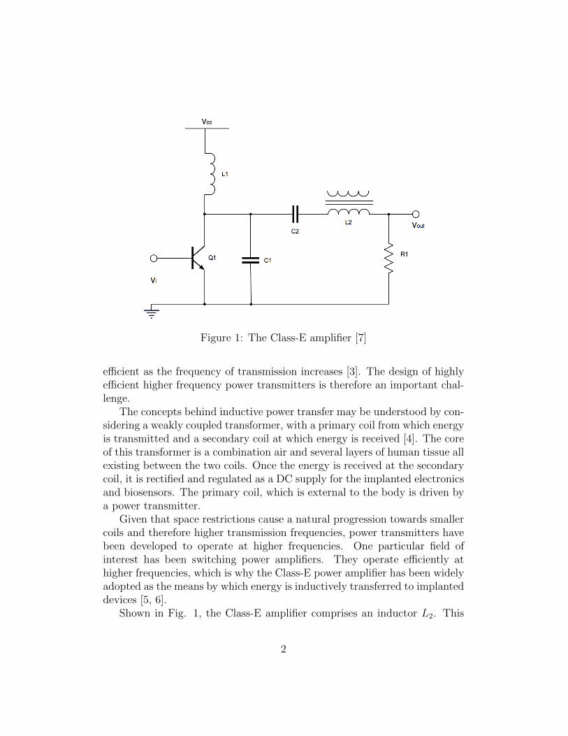
Figure 1: The Class-E amplifier [7]
efficient as the frequency of transmission increases [3]. The design of highlyefficient higher frequency power transmitters is therefore an important chal-lenge.
The concepts behind inductive power transfer may be understood by con-sidering a weakly coupled transformer, with a primary coil from which energyis transmitted and a secondary coil at which energy is received [4]. The coreof this transformer is a combination air and several layers of human tissue allexisting between the two coils. Once the energy is received at the secondarycoil, it is rectified and regulated as a DC supply for the implanted electronicsand biosensors. The primary coil, which is external to the body is driven bya power transmitter.
Given that space restrictions cause a natural progression towards smallercoils and therefore higher transmission frequencies, power transmitters havebeen developed to operate at higher frequencies. One particular field ofinterest has been switching power amplifiers. They operate efficiently athigher frequencies, which is why the Class-E power amplifier has been widelyadopted as the means by which energy is inductively transferred to implanteddevices [5, 6].
Shown in Fig. 1, the Class-E amplifier comprises an inductor L2. This
2

(a)
(b)
(c)
Figure 2: Class-E amplifier timing diagrams at 27MHz (a) vin (b) vC1 and(c) vout.
3

Figure 3: A common emitter colpitts oscillator.
4
(a)
(b)
(c)
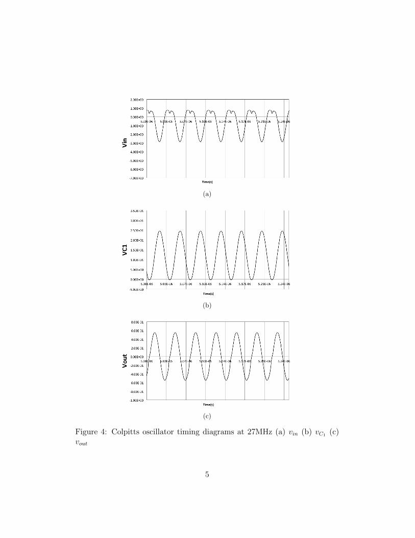
Figure 4: Colpitts oscillator timing diagrams at 27MHz (a) vin (b) vC1 (c)vout
5

(a)
(b)
Figure 5: (a) The Class-E oscillator with a Colpitts network [8], (b) with aHartley feedback network
6

(a)
(b)
(c)
Figure 6: Class-E oscillator timing diagrams based on [8] (a) vin (b) vC1 and(c) vout.
7

inductor represents the primary coil for the transmission of wireless energyto an implanted device. The amplifier’s efficiency at high frequencies is at-tributed to its ability to hold zero charge across the terminals of the transistorwhile it is switching. Not only is the voltage designed to be zero, but so isthe rate of change of voltage (dv/dt) according to [7, 9]. A simulated timingdiagram of a 27MHz Class-E amplifier is presented in Fig. 2, with the inputclock signal vin, voltage across C1 (vC1) and load voltage vout. An obser-vation of vC1 shows that after a transistor delay, the voltage drops prior toswitching according to the principles of the Class-E amplifier. This allows fora power amplifier which efficiently transmits energy across L2 according tothe switching frequency supplied by the input voltage vin. The capacitor C1
also absorbs parasitic capacitance that exists between transistor terminals,which becomes increasingly significant at higher frequencies where designparameters are in the order of parasitic impedances [7, 10, 9].
The Class-E amplifier works efficiently at high frequencies, however thefact that it is a switching power amplifier means that it requires a highfrequency square-wave input in order to operate effectively. This efficiencydoes not consider the energy that is required to produce the square-waveinput using a dedicated oscillator, be it a crystal or LC oscillator.
One example of an LC oscillator is the Colpitts oscillator, shown in Fig. 3.It is designed by selecting an inductor-capacitor combination that resonatesat a specified design frequency. The output signal of the oscillator is 1800 outof phase with the input signal. The feedback network then shifts the signal’sphase by another 1800 for the input of the transistor. Simulated timingdiagrams of a Colpitts oscillator are shown in Fig. 4. The input signal vinand feedback signal vC1 are 1800 out of phase, all sinusoidal. In order to usethe Colpitts oscillator as an input to a switching power amplifier, the outputmust past through an inverter in order to produce a square signal.
Generally speaking, the purpose of an oscillator is to generate a stableoscillating signal at a specific frequency. Similarly, the purpose of a poweramplifier is to use a pre-existing square-wave signal and boost its power level.In most literature regarding the design of wireless power transmitters for im-plantable devices, these two blocks are considered separate as indicated inFig. 7, yet both are necessary for the supply of inductive power. The combi-nation of both an oscillator and power amplifier may reduce the complexityand increase the overall efficiency of a power transmitter. An example ofsuch a circuit is presented in literature as a Class-E oscillator as shown inFig. 5(a) [8, 11, 12, 13].
8

(a)
(b)
Figure 7: Block diagrams indicating (a) separate power amplifier and oscil-lator blocks, and (b) combined power oscillator blocks.
Additional circuit elements have been added to the Class-E amplifier ofFig. 1 to form the Class-E oscillator of Fig. 5(a), namely the feedbackelements C3, C4 and L3. It was designed by Ebert et al. to constructivelyshift the phase of the feedback point of the oscillator [8]. The diode D1 isplaced at the input of the transistor in order to clip the input signal such thatit appears as a square wave, satisfying the requirement of the Class-E circuitto have a square-wave input. A simulated timing diagram of the Class-Eoscillator [8] is shown in Fig.6 with the input, feedback and output signalsvin, vC1 and vout respectively. Comparing the timing diagrams of the Class-Eamplifier and Colpitts oscillator, it is possible to identify that the Class-Eoscillator can be considered as a combination of these two circuits. Thefeedback network of the Class-E oscillator is similar to that of the Colpittsoscillator. It is also interesting to consider implementing a Hartley feedbackClass-E oscillator, conceptualised in Fig. 5(b).
Low power consumption is advantageous in biomedical systems, so ratherthan implementing oscillators and Class-E power amplifiers for wireless powertransmission it may be advantageous to consider a Class-E self-oscillator [5].Similar to the power amplifier, the Class-E self-oscillator would transmitenergy through L2. This idea will be investigated in subsequent sections of
9
this paper, including a measured comparison of different topologies, circuitdesign and modelling and an example of inductive wireless power transferusing a Class-E self-oscillator.
2. Comparison of Class-E Topologies
The Class-E amplifier is currently a popular choice in transmitting wire-less inductive power, however the use of Class-E self-oscillators is a potentialimprovement. In this paper a number of different Class-E circuits are com-pared using laboratory measurements. The circuits include a Class-E am-plifier, Class-E self-oscillator with LC feedback, and a Class-E self-oscillatorwith a crystal feedback link.
In order to determine whether using a Class-E oscillator is advantageousover a Class-E amplifier, similarly designed circuits have been constructedand tested with the main circuit elements chosen to be as similar as possi-ble. The transistor used for all of the five circuits is BC547B from FairchildSemiconductors. The elements of the Class-E circuits have been determinedaccording to [9], and all of the circuits are supplied with a 3V supply. Theinductor L2 is in fact a spiral inductor, forming the primary coil for thetransfer of inductively transferred power.
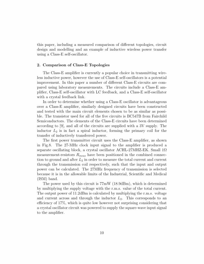
The first power transmitter circuit uses the Class-E amplifier, as shownin Fig.8. The 27-MHz clock input signal to the amplifier is produced aseparate oscillating block, a crystal oscillator ACHL-27MHZ-EK. Small 1Ωmeasurement-resistors Rmeas have been positioned in the combined connec-tion to ground and after L2 in order to measure the total current and currentthrough the transmission coil respectively, such that the input and outputpower can be calculated. The 27MHz frequency of transmission is selectedbecause it is in the allowable limits of the Industrial, Scientific and Medical(ISM) band.
The power used by this circuit is 77mW (18.9dBm), which is determinedby multiplying the supply voltage with the r.m.s. value of the total current.The output power of 11.2dBm is calculated by multiplying the r.m.s. voltageand current across and through the inductor L2. This corresponds to anefficiency of 17%, which is quite low however not surprising considering thata crystal oscillator circuit was powered to supply the square-wave input signalto the amplifier.
10

Figure 8: A 27MHz Class-E amplifier constructed in hardware, driven by acrystal oscillator.
2.1. Class-E Oscillators biased with Resistors
The next step of the comparison involves the construction of the Class-Eself-oscillator circuit, shown in Fig.9. This differs from the Class-E oscillatorshown in Fig. 5(a) in that the load is represented by the inductor L2 ratherthan a resistor. Other proposals involve using a capacitor as a feedbacknetwork [14], however the feedback point in this experiment is taken betweenthe L2 and C2 component of the Class-E amplifier, and consists of an LC pairin order to reverse the phase difference that is incurred at the point acrossL2 to increase efficiency. The element between the base and emitter of Q1 isa 100kΩ biasing resistor. The power used by this circuit is 35mW (15.5dBm)and 11.4dBm is transmitted, corresponding to an efficiency of 39%. Whilethis is much higher than the efficiency of the Class-E Amplifier of Fig.8, the34MHz frequency of the output is higher than the desired 27MHz value. Thisis due to the fact that the accuracy of the circuit’s frequency is controlledsolely by the accuracy of its individual inductor and capacitor values.
A variant of this circuit has been implemented by inserting a 27MHzcrystal (Citizen America CS1027.000MABJ-UT) as the feedback network inorder to create a stable frequency. This crystal is not an oscillator itself,but an accurate impedance that ensures the input frequency to the transis-tor is 27MHz. The schematic of this circuit is shown in Fig.10, with thebase-emitter element being 100kΩ resistor. The power used by the circuithas been measured to be 112mW (20.5dBm) and the output power is also20.5dBm, which corresponds to a measured efficiency of 100%. This is at-tributed to negligibly small losses in the biasing circuit of the amplifier andzero-switching conditions at the collector of the transistor.
11

Figure 9: Schematic diagram of a Class-E oscillator with an LC feedbacknetwork and element between the transistors base and emitter terminals,being either a 100kΩ resistor or a Schottky diode.
Figure 10: Schematic diagram of a Class-E oscillator with a 27MHz Crys-tal feedback network and element between the transistors base and emitterterminals, being either a 100kΩ resistor or a Zener diode.
12
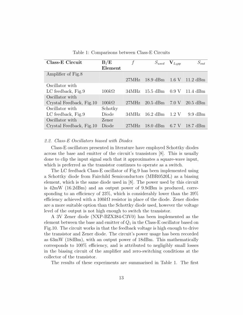
Table 1: Comparisons between Class-E Circuits
Class-E Circuit B/E f Sused VL2pp Sout
ElementAmplifier of Fig.8
27MHz 18.9 dBm 1.6 V 11.2 dBmOscillator withLC feedback, Fig.9 100kΩ 34MHz 15.5 dBm 0.9 V 11.4 dBmOscillator withCrystal Feedback, Fig.10 100kΩ 27MHz 20.5 dBm 7.0 V 20.5 dBmOscillator with SchotkyLC feedback, Fig.9 Diode 34MHz 16.2 dBm 1.2 V 9.9 dBmOscillator with ZenerCrystal Feedback, Fig.10 Diode 27MHz 18.0 dBm 6.7 V 18.7 dBm
2.2. Class-E Oscillators biased with Diodes
Class-E oscillators presented in literature have employed Schottky diodesacross the base and emitter of the circuit’s transistors [8]. This is usuallydone to clip the input signal such that it approximates a square-wave input,which is preferred as the transistor continues to operate as a switch.
The LC feedback Class-E oscillator of Fig.9 has been implemented usinga Schottky diode from Fairchild Semiconductors (MBR0520L) as a biasingelement, which is the same diode used in [8]. The power used by this circuitis 42mW (16.2dBm) and an output power of 9.9dBm is produced, corre-sponding to an efficiency of 23%, which is considerably lower than the 39%efficiency achieved with a 100kΩ resistor in place of the diode. Zener diodesare a more suitable option than the Schottky diode used, however the voltagelevel of the output is not high enough to switch the transistor.
A 3V Zener diode (NXP-BZX384-C3V0) has been implemented as theelement between the base and emitter of Q1 in the Class-E oscillator based onFig.10. The circuit works in that the feedback voltage is high enough to drivethe transistor and Zener diode. The circuit’s power usage has been recordedas 63mW (18dBm), with an output power of 18dBm. This mathematicallycorresponds to 100% efficiency, and is attributed to negligibly small lossesin the biasing circuit of the amplifier and zero-switching conditions at thecollector of the transistor.
The results of these experiments are summarised in Table 1. The first
13

significant point of note is that using a feedback network in the Class-E circuitimproves the efficiency of the transmitter, in that a dedicating oscillating unitis no longer required.
Another significant point is that including a crystal in the feedback net-work allows the frequency of the transmitter to be controlled, rather thanrelying on the accuracy of individual inductors and capacitors, which maycause unstable or inaccurate transmission frequencies.
The use of zener diodes on the base of the circuit’s transmitter makeslittle difference on the performance of the amplifier, however it may be animportant to regulate the output of the transmitter in the case that thefeedback voltage becomes too high.
3. Modelling the Class-E Oscillator
It is determined that the Class-E self-oscillating circuit with the crystalfeedback link is the most efficient and stable of the three options presented inSection 2. A higher-powered version of Class-E self-oscillator circuit of Fig.10 is shown in Fig.11. This circuit may be further understood by viewing itin its signal model shown in Fig. 12. The load network at the collector ofthe transistor is of particular interest. The quartz crystal consumes verylittle current in comparison to the load network, making it negligible inthe determination of ZL. The choke inductor L1 can also be large enoughto ignore with respect to the load network of the oscillator such that ZL
becomes:
ZL =1
sC1
||(
1
sC2
+ L2 +RL
)(1)
If the output of the circuit is seen as the voltage across the transmittinginductor L2 and R, the output voltage of the signal becomes:
vout = βibsL2 +RL
sL2 +RL + 1sC2
ZL (2)
and the transfer function becomes:
voutvin
= KsL2C2 +RLC2
s2L2C1C2 + sRLC1C2 + s(C1 + C2)(3)
where K is a scalar related to the transistor’s βib base-emitter resistancerbe and input voltave vin.
14

Figure 11: Schematic diagram of a Class-E oscillator with a 27MHz Crys-tal feedback network and element between the transistors base and emitterterminals, being either a 100kΩ resistor or a Zener diode [15].
Figure 12: A small signal model of the Class-E self-oscillator of Fig. 11
15
This presents a second order system, the circuit elements of which maybe determined by manipulating the transfer function’s resonant frequency ωand damping factor ζ. Based on (3) these terms are determined by:
ω =1√
L2C1||C2
(4)
ζ =RL
2
√C1||C2
L2
(5)
Given that the intended resonant frequency ω is known, and that thecoil’s properties L2 and RL have been determined, it is possible to deter-mine expressions from the simultaneous equations (4) and (5) to determineexpressions for ζ and C1||C2 as (6) and (7) respectively.
ζ =RL
2ωL2
(6)
C1||C2 =2ζ
RLω(7)
Once C1||C2 has been calculated, the next step involves the selection ofindividual capacitor values C1 and C2. If C1 is larger than C2, it will chargeand discharge quicker. This implies that the voltage across C1 will drop tozero quicker as charge enters the larger capacitor C2. It is important that thisvoltage drops before the transistor switches states so as to avoid dischargelosses.
4. Wireless Power Transfer
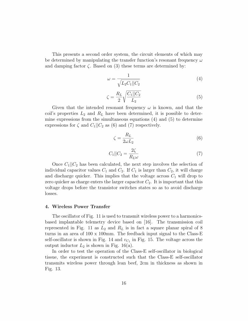
The oscillator of Fig. 11 is used to transmit wireless power to a harmonics-based implantable telemetry device based on [16]. The transmission coilrepresented in Fig. 11 as L2 and RL is in fact a square planar spiral of 8turns in an area of 100 x 100mm. The feedback input signal to the Class-Eself-oscillator is shown in Fig. 14 and vC1 in Fig. 15. The voltage across theoutput inductor L2 is shown in Fig. 16(a).
In order to test the operation of the Class-E self-oscillator in biologicaltissue, the experiment is constructed such that the Class-E self-oscillatortransmits wireless power through lean beef, 2cm in thickness as shown inFig. 13.
16

Figure 13: Experimental set up with the transmission coil, lean beef, stackedspiral receiving coil and meat.
The receiving coil is a stacked spiral coil from [15]. Stacking planar spiralinductors increases parasitic capacitance, which allows the stacked spiral coilto operate at a lower self-resonant frequency compared with an equivalentplanar spiral. The stacked spiral is contained within a 10mm x 10mm x4.5mm volume and the voltage across the coil after the wireless transferthrough meat is shown in Fig. 16(b).
The power sent by the Class-E oscillator is 27.5dBm, and the receivedpower on the stacked spiral 20.6dBm, implying that a path loss of just 6.9dBoccurred.
5. Conclusion
This paper proposes the use of Class-E oscillators of a particular topologyas inductive power transmitters for implanted telemetry devices that transmitinformation read by biosensors. In most literature regarding inductive powertransfer for biodevices, power amplifiers and oscillators are considered as twoseparate blocks. By combining these topologies into a self-oscillating powertransmitter, greater efficiency can be achieved. Several Class-E self-oscillatortopologies were compared with the commonly used Class-E amplifier. TheClass-E oscillators were determined to be more efficient when considering thepower used by the input signal to the amplifier.
Different feedback options are compared amongst Class-E oscillators, andit is proposed that a crystal feedback network ensures a more efficient circuit
17
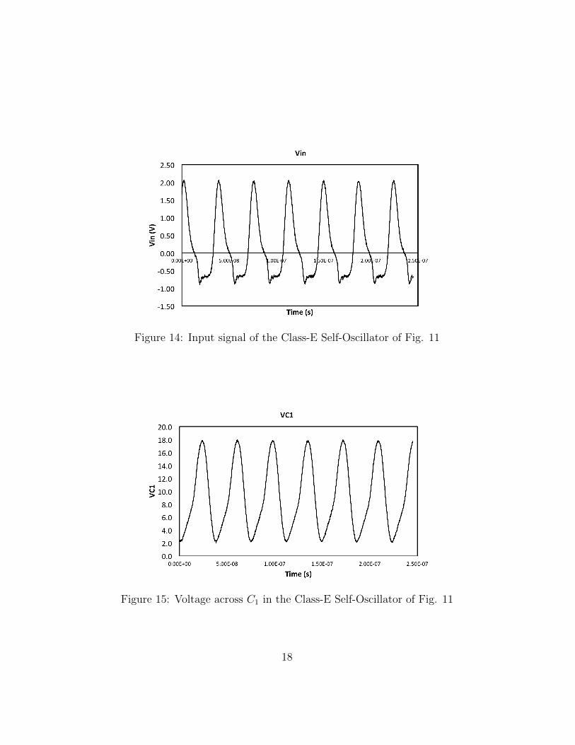
Figure 14: Input signal of the Class-E Self-Oscillator of Fig. 11
Figure 15: Voltage across C1 in the Class-E Self-Oscillator of Fig. 11
18

(a)
(b)
Figure 16: Voltage signals across (a) the transmission coil of he Class-Eself-oscillator of Fig. 11, and (b) the receiving coil after the biological tissue.
with a more stable and better controlled frequency. The use of Zener diodesat the input of the oscillator is determined to be advantageous when operatingat higher input voltage levels, in that the input is clipped to the diode’svoltage rating, allowing the Class-E load to operate as designed.
19
The Class-E load network was modelled as a second-order system, whichallowed for a straightforward design process based on second order variables.
A higher-power Class-E oscillator was implemented based on the resultsof the circuit comparisons, and used to transmit power through a biologicalmuscle environment using 2cm thick beef. The received power successfullypowered the telemetry device implanted in biological tissue.
[1] B. Lenaerts, R. Puers, Inductive powering of a freely moving system,Sensor Actuat A-Phys 123-24 (2005) 522–530.
[2] M. Catrysse, B. Hermans, R. Puers, An inductive power system withintegrated bi-directional data-transmission, Sensor Actuat A-Phys 115(2004) 221–229.
[3] P. Vaillancourt, A. Djemouai, J. Harvey, M. Sawan, Em radiation be-havior upon biological tissues in a radio-frequency power transfer link fora cortical visual implant, Proceedings of the 19th Annual InternationalConference of the IEEE Engineering in Medicine and Biology Society 6(1997) 2499–2502 vol.6.
[4] Z. Yang, W. Liu, E. Basham, Inductor modeling in wireless links forimplantable electronics, IEEE Transactions on Magnetics 43 (2007)3851–3860.
[5] C. Zierhofer, E. Hochmair, High-efficiency coupling-insensitive transcu-taneous power and data transmission via an inductive link, BiomedicalEngineering, IEEE Transactions on 37 (1990) 716 – 722.
[6] B. Lenaerts, R. Puers, Automatic inductance compensation for class edriven flexible coils, Sensor Actuat A-Phys 145 (2008) 154–160.
[7] N. Sokal, A. Sokal, Class e-a new class of high-efficiency tuned single-ended switching power amplifiers, IEEE Journal of Solid-State Circuits10 (1975) 168–176.
[8] J. Ebert, M. Kazimierczuk, Class e high-efficiency tuned power oscilla-tor, IEEE Journal of Solid-State Circuits 16 (1981) 62 – 66.
[9] N. Sokal, Class-e switching-mode high-efficiency tuned rf/microwavepower amplifier: improved design equations, IEEE MTT-S InternationalMicrowave Symposium Digest 2 (2000) 779–782 vol.2.
20

[10] M. Kazimierczuk, Class e tuned power amplifier with nonsinusoidaloutput voltage, IEEE Journal of Solid-State Circuits 21 (1986) 575–581.
[11] M. Kazimierczuk, A new approach to the design of tuned power os-cillators, IEEE Transactions on Circuits and Systems 29 (1982) 261 –267.
[12] V. Krizhanovski, D. Chernov, M. Kazimierczuk, Low-voltage electronicballast based on class e oscillator, IEEE Transactions on Power Elec-tronics 22 (2007) 863 – 870.
[13] M. Kazimierczuk, V. Krizhanovski, J. Rassokhina, D. Chernov, Class-emosfet tuned power oscillator design procedure, IEEE Transactions onCircuits and Systems I: Regular Papers 52 (2005) 1138 – 1147.
[14] Q. Ma, M. Haider, S. Yuan, S. Islam, Power-oscillator based high effi-ciency inductive power-link for transcutaneous power transmission, 53rdIEEE International Midwest Symposium on Circuits and Systems (2010)537 – 540.
[15] A. N. Laskovski, T. Dissanayake, M. R. Yuce, Stacked spirals for biosen-sor telemetry, IEEE Sensors Journal 11 (2011) 1484 – 1490.
[16] A. N. Laskovski, M. R. Yuce, Harmonics-based bio-implantable teleme-try system, 30th Annual International Conference of the IEEE Engi-neering in Medicine and Biology Society (2008) 3196 – 3199.
21