circuit design and technological limitations of silicon...
TRANSCRIPT
Circuit Design and Technological Limitations ofSilicon RFICs for Wireless Applications
by
Donald A. Hitko
Bachelor of Science in Electrical EngineeringGMI Engineering & Management Institute, 1994
Master of Science in Electrical Engineering and Computer ScienceMassachusetts Institute of Technology, 1997
Submitted to the Department of Electrical Engineering and Computer Sciencein partial fulfillment of the requirements for the degree of
Doctor of Philosophy in Electrical Engineering and Computer Science
at the
MASSACHUSETTS INSTITUTE OF TECHNOLOGY
June 2002
Massachusetts Institute of Technology, 2002. All Rights Reserved.
Author __________________________________________________________
Department of Electrical Engineering and Computer ScienceMay 24, 2002
Certified by _______________________________________________________
Charles G. SodiniProfessor of Electrical Engineering and Computer Science
Thesis Supervisor
Accepted by ______________________________________________________
Arthur C. SmithChairman, Committee on Graduate Students
Department of Electrical Engineering and Computer Science

2

ionges infects
theie on
nduponcusesper-man-henalsrthis
ing-e a
itstionre the andbernol-
Circuit Design and Technological Limitations of Silicon RFICsfor Wireless Applications
by
Donald A. Hitko
Submitted to the Department of Electrical Engineering and Computer Scienceon May 24, 2002, in partial fulfillment of the requirements for the degree of
Doctor of Philosophy in Electrical Engineering and Computer Science
Abstract
Semiconductor technologies have been a key to the growth in wireless communicatover the past decade, bringing added convenience and accessibility through advantacost, size, and power dissipation. A better understanding of how an IC technology afcritical RF signal chain components will greatly aid the design of wireless systems anddevelopment of process technologies for the increasingly complex applications that lthe horizon. Many of the evolving applications will embody the concept ofadaptive per-formance to extract the maximum capability from the RF link in terms of bandwidth,dynamic range, and power consumption—further engaging the interplay of circuits adevices is this design space and making it even more difficult to discern a clear guidewhich to base technology decisions. Rooted in these observations, this research foon two key themes: 1) devising methods of implementing RF circuits which allow theformance to be dynamically tuned to match real-time conditions in a power-efficient ner, and 2) refining approaches for thinking about the optimization of RF circuits at tdevice level. Working toward a 5.8GHz receiver consistent with 1GBit/s operation, sigpath topologies and adjustable biasing circuits are developed for low-noise amplifier(LNAs) and voltage-controlled oscillators (VCOs) to provide a facility by which powecan be conserved when the demand for sensitivity is low. As an integral component ineffort, tools for exploring device level issues are illustrated with both circuit types, helpto identify physical limitations and design techniques through which they can be mitigated. The design of two LNAs and four VCOs is described, each realized to providfully-integrated solution in a 0.5µm SiGe BiCMOS process, and each incorporating allbiasing and impedance matching on chip. Measured results for these 5-6GHz circuallow a number of poignant technology issues to be enlightened, including an exhibiof the importance of terminal resistances and capacitances, a demonstration of whetransistor fT is relevant and where it is not, and the most direct comparison of bipolarCMOS solutions offered to date in this frequency range. In addition to covering a numof new circuit techniques, this work concludes with some new views regarding IC techogies for RF applications.
Thesis Supervisor: Charles G. SodiniTitle: Professor of Electrical Engineering and Computer Science


earter’s,tail
pro-dif-I still
thatthanen-heregrad-und
ed thehingther
n thosehave ajob-e, forthoseinty-. Myiethose
h meut theful.
mingse atnts.chere
berin
Acknowledgments
Wow! Maybe that says it all. I can remember when it took me by surprise to ha colleague mention taking five years to complete the Ph.D.—five years after the Masthat is. How little I knew then what deciding to continue beyond the Master’s would enfor me. But I recall another colleague attributing his decision to stay for the Ph.D.gram to thinking: “It seemed like a pretty neat place to spend a few years.” Albeit at aferent location, and although “a few years” may have proven to been a euphemism,found his statement to hold throughout my time here.
Attending graduate school at a university like MIT is mostly about the peopleit brings together, for this is what makes the experience so rewarding. But ratherimplicating anyone, I would instead like to express my gratitude to each of you by mtioning some of your personal contributions which have meant so much to me. Sogoes, in no discernible order. First, thank you for assuring me that I was born to be auate student. How right you were. Thank you for the Tosci’s runs, and for being arothe group almost as long as I have been. Thanks to those who collectively surmountphenomenon of always playing one bad inning. Thank you for the time spent crustennis balls, and for waiting in perpetuum for a window seat. Thanks for getting togeto work on calendar pages, and to the many predecessors here who were featured ipages. Thanks to those with whom hallway hockey was anointed. Perhaps we canreunion in 30 years to see if the puck is still there. Thank you for the many helpfulrelated discussions, for sustaining some semblance of organization about the officalways being upbeat, and for infusing new enthusiasm into the group. Thanks towho provided helpful advice on FFTs, replica biasing techniques, device noise, pohaired pursuits, computers, the art of Re-use, RF circuits, and when to shoot the puckapologies if I did not do particularly well in taking the advice. Thank you for the dphotos, which dressed up numerous presentations as well as this thesis. Thanks towho made playing (and coaching!) hockey so much fun, and to those who put up wittaking their P.E. classes six times. Of course, this would not have happened withoinitial encouragement to get started on the hockey “hobby”, for which I am very thankThank you for always putting on a good show whenever I came to watch, and for coto watch my feeble efforts. Thank you for the Esplanade skates, and especially tho2AM. Thank you for getting up at 4AM to observe re-enactments of historical eveFinally—although still in no discernible order—thank you for the 1AM dinners (of whiMom would not approve) and for ice cream in (on?) fire trucks; I’m glad I could be thfor your 48th.
In their support of this work, we are indebted to SRC (through contract num2000-HJ-794), IBM Microelectronics in Burlington, Vermont, and HRL Laboratories
5

Acknowledgments
meHRLtions, and
evenouhom
re oningof theestions
f myer’s36thwishrest
setts.
ger”ood
Malibu, California. With a big assist from Jeff Gross, the folks at IBM supplied soexcellent focused-ion beam rework to enable experimentation with the oscillators.lent their support through a fellowship, making space for me on two of their IC fabricaruns, providing access to noise measurement equipment for amplifiers and oscillatorby continually demonstrating their remarkable patience.
The readers of this thesis have proven nothing short of amazing, a task mademore daunting by my manner of writing and lack of a knack for timing. A big thank yto Charles Sodini, Jesús del Alamo, Hae-Seung Lee, and Dan McMahill, each of ware undoubtedly grateful that FrameMaker® has no provision for footnoting a footnote. Inparticular, Charlie deserves a commendation for being dragged through this procedumy behalf with two thesesand an area examination. Discussions with Jesús regarddevices and noise have always been very enlightening. I am also very appreciativetime Dan has spent on this, as he has offered a great deal of insight and many suggwhich are reflected throughout this work.
Of course, none of this would have occurred without the unwavering support ofamily. To my parents, may you both enjoy a relaxed forthcoming Father’s Day (MothDay wishes were passed along in my Bachelor’s thesis) and a happy (upcoming)anniversary. I’d also like to congratulate Trisha and Eric for their perseverance, andyou continued good tidings with the restaurant. Finally, many thanks are owed to theof the family for keeping up with me during my extended disappearance to Massachu
As for what comes next, well, we will have to see. But as a start, the late “BadBob Johnson might have said it best in noting, “It’s a great day for hockey.” Sounds gto me.
Donald A. HitkoCambridge, MassachusettsMay 29, 2002
6

......17....18.....19
......21
.......24
.....25......30
......33
.....35
.....37
....40
...44
...47
....51
.....55
....65
.......74
.....79
....8387
Table of Contents
Acknowledgments 5
Introduction 15
1.1 Thesis Contributions .............................................................................................1.1.1 Optimization of RF Circuits at the Device Level ............................................1.1.2 Trade-off Between Quality of Service and Power Consumption ...................
1.2 A Preview of the Thesis........................................................................................
An Approach to Spiral Inductor Modeling 23
2.1 Integrated Inductances .........................................................................................
2.2 Selected Recent Efforts in Spiral Inductor Modeling............................................2.2.1 Alternative Inductance and Series Resistance Formulations.........................
2.3 Spiral Inductor Loss Mechanisms.........................................................................2.3.1 Inductor Quality Factor...................................................................................
2.4 Quick Turn Models for Spiral Inductors................................................................
Appendix: Calculation of Inductor Quality Factor ........................................................
Time-Variant System Modeling 43
3.1 A Plausibility Argument for Time-Variant Models.................................................
3.2 Oscillator Analysis Using a Linear Time-Variant Model........................................
3.3 Optimizing Devices and Technology for Oscillators..............................................
3.4 Cyclostationarity in Oscillators..............................................................................
3.5 Extending the Linear Time-Variant Model to Mixers ............................................
Low-Noise Amplifiers 73
4.1 Impedance Matching............................................................................................
4.2 Technology Considerations for LNAs...................................................................
4.3 Alternative LNA Topologies ..................................................................................4.3.1 Unity Current Gain Frequency (fT) Doubler .......................................................
7

Contents
.......89
.....91
....93
......98
..100
..102...103....110...116..123
...126....127..130..133..137
....139
.....150
..156....158.161.164...165...169
...171
..173
..178...179
....181
.....191
4.3.2 Cascode.........................................................................................................4.3.3 Effects of Inductor Loss..................................................................................
4.4 Transistor and Amplifier Stability ..........................................................................
4.5 Lessons in Low Noise...........................................................................................
Appendix: Two-port Stability Circles............................................................................
An Exercise in Designing Low-Noise Amplifiers 101
5.1 A Bipolar 5.8GHz LNA Design .............................................................................5.1.1 Output Matching Network Design..................................................................5.1.2 Operating at Reduced Power Consumption Levels .......................................5.1.3 A Switched Current Source Bias Circuit ........................................................5.1.4 Layout Design of the 5.8GHz Switched-Stage LNA ......................................
5.2 CMOS LNA Design...............................................................................................5.2.1 Noise in CMOS Transistors ...........................................................................5.2.2 A 5.8GHz CMOS LNA ...................................................................................5.2.3 Stabilized Biasing for the CMOS LNA ...........................................................5.2.4 Layout Design of the 5.8GHz CMOS LNA ....................................................
5.3 Measured Results for the 5.8GHz LNAs..............................................................
5.4 Lessons in Low Noise: The Sequel......................................................................
An Experiment with Voltage-Controlled Oscillators 155
6.1 A Family of Bipolar 5.8GHz VCOs .......................................................................6.1.1 Transistor Considerations in Oscillators........................................................6.1.2 A Differential Colpitts Oscillator......................................................................6.1.3 Biasing Circuitry for the Bipolar Oscillators ....................................................6.1.4 An Impedance-Matched Output Buffer ..........................................................6.1.5 Layout Design of the Bipolar VCOs...............................................................
6.2 A CMOS 5.8GHz VCO Design.............................................................................6.2.1 Adaptive Biasing of the CMOS Oscillator ......................................................6.2.2 An Impedance-Matched Output Buffer in CMOS...........................................6.2.3 Layout Design of the CMOS VCO.................................................................
6.3 Measured Results for the 5.8GHz VCOs..............................................................
6.4 Observations on Oscillators .................................................................................
Final Thoughts 195
Bibliography 201
8

......16
......26
......27
......34
.......38
...40
....45
.....46
......48
....50
.......52
.....53
.......54
llator
.......56
nded.....58
rces.....60
......61
.....63
......66
List of Figures
1-1 System dynamics model for IC technology-based markets..................................
2-1 Coupled line segment model proposed by Long and Copeland [12]. ..................
2-2 Compact lumped-element model for an inductor on a silicon substrate. .............
2-3 Loss mechanisms in a spiral inductor...................................................................
2-4 Geometry parameters describing a square spiral inductor...................................
2-5 Circuit model for calculation of inductor quality factor..........................................
3-1 Pictorial argument for a time-variant oscillator model, adapted from [34]............
3-2 Simplified schematic of a single-balanced mixer..................................................
3-3 Calculation of the impulse sensitivity of an oscillator; (a) steady-state oscillationvoltage, (b) current injected to approximate an impulse function input,(c) impulse perturbation response compared with the steady-state oscillation,(d) phase of the output signal in the perturbation response. ............................
3-4 Typical oscillator impulse sensitivity function.......................................................
3-5 Schematic of single-ended oscillator used in noise analysis. ..............................
3-6 Bipolar transistor with terminal parasitic elements. ..............................................
3-7 ISFs associated with transistor terminal resistances............................................
3-8 Transistor collector (a) and base (b) currents calculated for the single-ended osciexample; the terminal currents are marked with x’s and the components thatgenerate shot noise are shown with the solid traces. ......................................
3-9 Schematic used to solve for the transistor displacement currents in the single-eoscillator example. ............................................................................................
3-10 Calculation of the effective ISFs for the collector (a) and base (b) shot noise soufor the single-ended oscillator example. ...........................................................
3-11 Calculation of phase noise for single-ended oscillator example. .......................
3-12 Demonstration of the potential effect of transistor displacement currents in thecalculation of oscillator phase noise. ................................................................
3-13 Single-balanced mixer schematic for noise simulation. .....................................
9

Figures
nse
.......67
e tolse
.....68
......69
.....70
lifier.......77
fierthe.......78
itter
......83
....88
......90
.....90
.....94
......95
....96
.....102
...104
....107
(Qs
m
n a...108
...114
3-14 Calculation of the impulse response of a mixer; (a) impulse perturbation respocompared with the steady-state condition, (b) applied impulse and calculatedimpulse response.............................................................................................
3-15 Mixer response to noise injected at the input of the switching pair; (a) responsimpulses injected at moments throughout one LO period, (b) 2-D DFT of impuresponse data giving conversion gain for noise about each LO harmonic as afunction of the chosen IF. .................................................................................
3-16 SPICE statement for a periodic current impulse. ...............................................
3-17 Calculation of the noise in a mixer resulting from the input transconductor; (a)conversion gains from input of switching pair to an IF output at 800MHz, (b)equivalent output current noise from RF transconductor stage. .......................
4-1 Input impedance-matching using an emitter inductance in a common-emitter ampstage. ...............................................................................................................
4-2 Effect of emitter inductance on the input impedance of a common-emitter amplistage where the arrows indicate the direction of increasing LE; correlation in equivalent input noise sources has been neglected. ........................................
4-3 Illustration of achieving a simultaneous noise and power match in a common-emtransistor stage; correlation in the equivalent input noise sources has beenneglected. .........................................................................................................
4-4 Battjes’ fT doubler circuit. ......................................................................................
4-5 Cascode amplifier stage with input impedance matching. ...................................
4-6 Intrinsic feedback within a common-emitter stage................................................
4-7 Source stability circles for a common-emitter transistor.......................................
4-8 Loop gain analysis of a common-emitter transistor. ............................................
4-9 Load stability circles for an emitter-follower transistor. ........................................
5-1 Cascode stage tuned for minimum noise at 5.8GHz. ..........................................
5-2 Design of the output matching network for the cascode LNA stage.....................
5-3 Cascode LNA gain stage tuned for 5.8GHz.........................................................
5-4 Evolution of noise figure (a) and gain (b) in a cascode LNA stage as inductor lossof 17-19) is included. In (a), the upper trace of each pair is the 50Ω noise figure(NF50) and the lower is the minimum noise figure (NFmin). In (b), each set of tracesrepresents the maximum available gain (Gma) and the available gain (Ga) for thecondition listed to the right, where Ga is labeled when it differs appreciably froGma. By convention, the maximum stable gain (Gms) is shown when Gma isundefined. Marked with the diamonds is for the matched stage whe50Ω impedance is provided by both the source and load.................................
5-5 RF signal path for the 5.8GHz switched-stage LNA. ...........................................
20 s21log
10
Figures
g.....115
...117
......118
..120
ighthe....122
d (b)...123
124
istor[76]..131
..132
.134
ce”
..135
38
A inr...140
losscateded
..141
so the
....143
(a),the
ntshe...145
5-6 Effects observed in the 5.8GHz LNA of adding the low power stage and includinparasitics associated with the pads, resistors, and capacitors. ........................
5-7 Effect of the bias coupling impedance on noise and linearity...............................
5-8 Concept for the base current source bias scheme. ..............................................
5-9 Biasing circuitry for the switched-stage 5.8GHz LNA. .........................................
5-10 Simulated performance of the 5.8GHz switched-stage LNA in both the (a,b) “hperformance” and (c,d) “low power” modes. Note the scale change between modes in representing the gain and noise figure..............................................
5-11 Simulated behavior of the 5.8GHz switched-stage LNA over (a) temperature ansupply variations. ..............................................................................................
5-12 Die photo of 5.8GHz switched-stage LNA IC (CMLNA-SW)..............................
5-13 Comparison of models for the minimum noise figure of a common-source transat two drain current levels. Solid lines represent results of the Shaeffer modeland dashed lines are simulation results using full BSIM3v3 models. ...............
5-14 RF signal path for the 5.8GHz CMOS LNA........................................................
5-15 Biasing circuitry for the 5.8GHz CMOS LNA. ....................................................
5-16 Simulated performance of the 5.8GHz CMOS LNA in both the “high performan(a,b) and “low power” (c,d) modes. Noise figure calculations are based uponBSIM3v3 circuit models which have not implemented induced gate noise......
5-17 Die photo of 5.8GHz CMOS LNA IC (CMLNA-CM)..........................................1
5-18 Measured noise figure (a) and gain (b) of the 5.8GHz switched-stage bipolar LNboth the high performance and low power modes. Note the shift in the centefrequency of the LNA pass band. .....................................................................
5-19 Measured s-parameter data for the 5.8GHz switched-stage LNA; the input return(a), gain (b), isolation (c), and output return loss (d) are shown. Solid traces indithe “default” bias conditions for operation at 3V. Measurements are also proviin the high performance mode for supply voltages of 2V (‘ ’), 2.5V (‘ ’), and 4V(‘ ’). ...................................................................................................................
5-20 Measured noise figure (a) and gain (b) of the 5.8GHz CMOS LNA at three biacurrent levels. Note the change in scales for the noise figure and gain relative tswitched-stage measurement plots. To improve legibility, Gahas only been shownat the 14mW setting.........................................................................................
5-21 Measured s-parameter data for the 5.8GHz CMOS LNA; the input return loss gain (b), isolation (c), and output return loss (d) are shown. Solid traces indicate“high performance” bias condition (4.67mA) for operation at 3V. Measuremeare also provided as the bias current is reduced to 2mA (‘ ’) and 1mA (‘ ’) with t3V supply..........................................................................................................
11

Figures
s...146
..157
to an...159
...162
..164
.166
mA...168
.170
...172
.174
ias...176
A in....177
..179
180
) fornce....183
,dthe....187
...188
in
for.....190
5-22 Measured input impedance (s11), output impedance (s22) and optimum noiseimpedance (Γopt) for the 5.8GHz switched-stage (a) and CMOS (b) LNAs. Arrowindicate the direction of increasing frequency. .................................................
6-1 A common-base Colpitts-style oscillator circuit. ...................................................
6-2 Primary contributions to oscillator phase noise from a transistor sized accordingLTI analysis. .....................................................................................................
6-3 The 5.8GHz bipolar oscillator core. ......................................................................
6-4 Biasing circuitry for the 5.8GHz bipolar oscillators. .............................................
6-5 Output buffer for the 5.8GHz bipolar oscillator family. .........................................
6-6 Simulated phase noise of the 5.8GHz bipolar VCO operating at 3V and with 6.25in the oscillator core..........................................................................................
6-7 Die photo of the 5.8GHz bipolar VCO IC (CMVCO). ...........................................
6-8 The 5.8GHz CMOS oscillator core. ......................................................................
6-9 Biasing circuitry for the 5.8GHz CMOS oscillator.................................................
6-10 Simulation of the DC behavior (a) and loop stability (b) of the CMOS oscillator bcircuit. ...............................................................................................................
6-11 Simulated phase noise of the 5.8GHz CMOS VCO operating at 3V and with 5mthe oscillator core.............................................................................................
6-12 Output buffer for the 5.8GHz CMOS oscillator...................................................
6-13 Die photo of 5.8GHz CMOS VCO IC (CMVCO-CM). ........................................
6-14 Measured spectrum and phase noise plots for the bipolar (a,b) and CMOS (c,d5.8GHz VCOs operated at 3V. The bias current in the oscillator core is 6mAthe bipolar VCO and 5.2mA for the CMOS version. Note the change in referelevel between the spectrum plots in parts (a) and (c).......................................
6-15 CMVCO phase noise behavior as a function of bias current and supply voltageexpressed as ratio of carrier power to noise power in a 1Hz bandwidth locate1MHz away from the carrier. Operation at voltages above 3V did not improvephase noise due to saturation in the biasing circuit..........................................
6-16 CMVCO-CM phase noise behavior as a function of power dissipation. ............
6-17 Technology comparison of phase noise behavior as a function of bias current oscillator core, expressed as a ratio of carrier power to noise power in a 1Hzbandwidth located 1MHz away from the carrier. A 3V supply has been usedthese measurements. .......................................................................................
12
...31
.149
..185
...191
List of Tables
2.1 Fitting Parameters for GMD Inductance Formulation, from Mohan, et al. [19] .....
5.1 Performance Summary for the C-band Monolithic Low Noise Amplifiers ............
6.1 Lumped-Element Model Parameter Summary for the Oscillator Inductor ............
6.2 Performance Summary for the C-band Monolithic VCOs ....................................
13

Tables
14
btedly
een a
es in
eased
nte-
ilities
ding to
upport
e, the
g yet
d for
uters,
ation
, and
ower
s of
Chapter 1
Introduction
One of the largest growth areas in electronics over the past decade has undou
been in applications of wireless communication. Semiconductor technologies have b
key to this growth, bringing added convenience and accessibility through advantag
cost, size, and power dissipation. Wireless products and systems thrive on this incr
utility, the commercial momentum of which has been fueling further investment in i
grated circuit designs and technology. The resulting advancement in system capab
has developed greater interest and receptiveness on the part of the consumer, lea
more applications being envisioned, and necessitating more available spectrum to s
the wireless infrastructure. To obtain this added bandwidth and alleviate interferenc
frequencies of the communication channels are necessarily edging upward, placin
more demands on the technologies used to implement the wireless systems.
Several recently opened ISM bands in the 5-6GHz range have been allocate
unlicensed operation of broadband wireless links between portable devices, comp
and the Internet. While always subject to change, the spirit of these National Inform
Infrastructure (NII) systems has been described by the FCC in a 1996 ruling [1]:
NII/SUPERNet devices [can] provide short-range, high-speed wireless dig-ital information transfer and could support the creation of new wirelesslocal area networks (LANs) as well as facilitate access to the NationalInformation Infrastructure without the expense of wiring. These devicesmay further the universal service goals of the Telecommunications Act byoffering schools, libraries, health care providers, and other users inexpen-sive networking alternatives which may access advanced telecommunica-tions services.
Three unlicensed bands are set aside by the ruling: 5.15-5.25GHz, 5.25-5.35GHz
5.725-5.875GHz, of which the band centered at 5.8GHz allows the highest transmit p
levels. With 150MHz of allotted bandwidth and up to 1W of transmit power, data rate
1GBit/s are conceivable over links covering short haul distances.
15

Chapter 1: Introduction
on-
based
ider-
the
cuit
e that
ich the
tures
ed in
ectric
port-
ay
stly a
rna-
ilicon
in a
ls or
it
n-s
While the products and applications in this field are still evolving, the one c
straint is that the consumer market will determine the acceptable end product price
on convenience, functionality, and a comparison with substitutes. Along with a cons
ation of form factor issues, the price the market will bear effectively sets a bound on
technologies which can be used in realizing the product. In conjunction with cir
design techniques, the limitations of these technologies determine the performanc
can be achieved in the required system components, a set of capabilities around wh
wireless link specifications must be drawn. These specifications in turn define the fea
and functionality, creating a reinforcing loop in the product design space as illustrat
Figure 1-1.
Size and cost constraints may, for example, make the use of a discrete diel
resonator oscillator impractical for the RF upconversion stage in the transmitter of a
able communications device. Integrating the RF link within a GaAs or InP MMIC m
yield good performance while addressing the size issues, but may represent too co
solution for the application. A circuit realized in silicon might be a less expensive alte
tive; however the transistor and passive device parasitics are more significant in a s
IC technology.1 For an oscillator, the increased transistor terminal parasitics result
higher phase noise, potentially interfering with weaker signals in adjacent channe
degrading the sensitivity of a receiver.2 In a transmitter, oscillator phase noise can lim
1 The semiconducting nature of silicon results in appreciable terminal capacitances to the sub-strate (e.g., collector-substrate capacitance in a bipolar transistor) which are not significant whesemi-insulating materials are used for the substrate material. Device designs in III-V semiconductors also typically employ mesa structures that lower access resistances and junction areawhen compared to more planar device topologies.
2 Oscillators and phase noise are covered in Chapter 3.
Price
TechnologiesFeatures &
PerformanceCircuitDesign
Figure 1-1. System dynamics model for IC technology-based markets.
16

Chapter 1: Introduction
e data
phase
wire-
izable
nol-
er-
that
po-
nolo-
ntal
king it
ning
s and
esign
ivers.
ighly
low a
, the
t
,
dygre
i-
how closely channels may be set which, for a fixed bandwidth, reduces the achievabl
rate. Conversely, by reducing the signal to noise ratio available to the demodulator,
noise in a receiver increases the bit error rate. Hence the noise of an oscillator in a
less communications system perceptibly impacts the allowable number of users, real
data rates, and the quality of the link, exemplifying the importance of the device tech
ogy. Making the right technology choice plays a crucial role in determining the comm
cial success of a product.
1.1 Thesis Contributions
Among the realizations from considering the nature of product development is
a better understanding of how an IC technology affects critical RF signal chain com
nents would greatly aid the design of both wireless systems and future process tech
gies for the increasingly complex applications that lie on the horizon. The fundame
interplay between devices and circuits in this design space confounds the issue, ma
difficult to discern a clear guide upon which to base technology decisions. In desig
key RF components—such as oscillators, mixers, and amplifiers—circuit technique
topologies can be developed to mitigate device limitations and to break traditional d
trade-offs by extending the concept of scalable circuit performance in radio transce
Furthermore, as the properties of a wireless communication channel tend to be h
uncertain, significant power savings can be realized by using circuits designed to al
dynamic adaptation to changing operating conditions. In light of these observations
focus of this thesis centers upon two key themes:
• The optimization of RF circuits at the device level. Two broad classes of circuitsare considered in this research: linear time-invariant (LTI) and linear time-varian(LTV). The LTI class of circuits is studied by designing and characterizing a pairof 5.8GHz low-noise amplifiers (LNAs), and the LTV side is investigated by con-structing and measuring a set of four voltage-controlled oscillators (VCOs).Approaches for exploring device level issues are developed with both circuit typeshelping to identify physical limitations and design techniques through which theycan be mitigated. Other RF circuits, such as mixers, can then be considerethrough these approaches as a combination of LTI and LTV elements. By carefullcrafting an experiment around a set of designs in a BiCMOS process and tracinmeasured circuit performance back to device level issues, some new views aoffered on directions that should be taken in IC technologies for RF applications.
• Devising methods of implementing RF circuits which allow the performance to bedynamically tuned to match real-time conditions in a power-efficient manner.Once the physical limitations are accommodated in the design, extracting the opt
17

Chapter 1: Introduction
ded
--
ions
hich
in the
s are
cor-
s the
bility
trained.
the
ents.
ant or
nals
ircuits
ts
t cir-
gains,
odic.
nisms
nnot
work
p-
s
mum performance from a technology becomes a matter of dissipating the requirepower in the circuit. It may not, however, be either necessary or feasible to operatthe transceiver circuits under this condition at all times. Signal path topologies anadjustable biasing circuits are developed to provide a facility by which power canbe conserved in RF circuits when the demand for performance is low, providingflexibility without compromising the operation when optimum performance isrequired. Incorporation of adaptability at the circuit and system levels is paramount in expanding the capabilities and increasing the utilization of wireless communication links, and yet remains a largely untapped resource in this field.
These themes represent two areas in which innovation will hold significant implicat
for the future of RF/microwave integrated circuits and the wireless applications in w
they are used. An introduction to these ideas and other related concepts is provided
following sections.
1.1.1 Optimization of RF Circuits at the Device Level
One of the salient characteristics of RF circuit design is that the active device
often pushed near their physical limits of operation, resulting in a high degree of
relation between the performance of an individual transistor and that of the circuit. A
signal frequency increases toward the rate where small-signal gains fall to unity, the a
to compensate device shortcomings through feedback mechanisms becomes cons
Thus, an important area of investigation for this regime of operation is to identify
device features that are limiting circuit performance in key RF transceiver compon
Most of the components can be represented by models of either the linear time-invari
linear time-variant variety. Through linearity, both models assume that the RF sig
being processed are small enough not to appreciably impact the operation of the c
that are processing them.3 Additionally, in LTI circuits, the parameters of the elemen
remain constant—a condition observed in many amplifiers and filters. Time-varian
cuits include oscillators, mixers, and prescalers, and are characterized by possessing
impedances, noise power, etc., which vary with time—often in a pattern that is peri
For both classes of circuits, models are discussed as a means of eliciting the mecha
responsible for constraining the circuit performance. However, this determination ca
be made in a vacuum, as circuit techniques and topologies can be developed to
around limitations (to an extent).4 Pushing the performance envelope in RF can only ha
pen through a concurrent optimization of circuits and technology.
3 A mixer processes either the RF or IF signal and produces the other; the applied oscillator drivecan be considered as creating a time-varying operating point for the signal and the noise sourcein the circuit. More will be said about mixers in Chapter 3.
4 Note the earlier point about the limited ability to implement compensation via feedback at RF.
18

Chapter 1: Introduction
ugh
s of a
g, and
F cir-
imits
tech-
ore
r noise
the
lim-
nefit.
cuits,
perfor-
n can
a
the
ay be
cess
cir-
and
red
rcuits.
ing at
But
upon
ower
eless
efined
Knowledge gleaned about the performance-limiting factors identified thro
these approaches can be applied at a number of levels. First, even within the confine
chosen process, a designer has considerable latitude with transistor selection, sizin
2-D layout geometry. These degrees of freedom may be used to better optimize R
cuits in pushing the limits of a technology, and to make more evident where those l
lie. Similarly, the tools described in this work can be used to guide the selection of a
nology for a chosen application. A bipolar or BiCMOS technology may involve m
masks than a comparable CMOS process, but the higher transconductance and lowe
per unit current of a bipolar transistor may provide advantages which can improve
quality of service to cost ratio of the overall system. Knowledge of the technological
itations yields insight into the extent to which performance can be expected to be
Finally, it is important to understand where device enhancements result in better cir
and where changes in the device needed to realize the enhancements may hurt
mance more than it helps. A thinner base and higher collector doping concentratio
be employed to increase the transistor fT,5 but whether a faster switching response and
higher current gain translate into improved RF circuits can be determined through
models that are proposed in the chapters which follow. Answers to such questions m
surprising, and are vital in setting directions for the continued development of IC pro
technologies.
As a direct illustration of the impact a transistor technology can have upon RF
cuit performance, comparative LNA and VCO designs are implemented in the CMOS
bipolar halves of a BiCMOS process. Different physical limitations are encounte
based on the devices being used, and thus different solutions are reflected in the ci
Each of the designs is geared toward a receiver in a 1GBit/s wireless network operat
5.8GHz, for which a high level of sensitivity may be required to support the data rate.
rather than choosing and designing to a given specification, the emphasis here is
finding the peak performance that can be extracted from a 0.5µm SiGe BiCMOS process,
and then determining how these limits change as a function of the technology and p
consumption.
1.1.2 Trade-off Between Quality of Service and Power Consumption
To meet consumer expectations in an increasingly sophisticated market, wir
communication systems need to provide an acceptable level of performance under d
5 The fT of a transistor is the frequency at which its current gain (in the common-emitter orcommon-source configurations) falls to unity, and is often used as a figure of merit in comparingdevices and technologies.
19

Chapter 1: Introduction
sup-
link.
d the
et of
less
acting
s of
are
tion
perfor-
elay,
eing
cern,
. In
sitivity
noise
be tol-
when
eak
pera-
cur-
erein,
noise
ut and
desir-
ider-
an
while
o
ency.
s are
the
, this
worst-case conditions. The interpretation of acceptability in these networks is one of
porting low latency, high data rate, ubiquitous access—necessitating a highly capable
However, it should be recognized that the data rates will not always be 1GBit/s an
channel may not always demand high sensitivity; designing to operate around a s
worst-case conditions drains power without always buying performance. When
demanding scenarios are common, the utility of the system may be increased by
upon real-time information about the link and the data being transmitted. Method
reducing power consumption by dynamically trading off quality of service levels that
not required may be feasible. By incorporating adaptability into RF circuits, the opera
of transceiver components can be adjusted so that power is never burned to support
mance levels—measured in terms of gain, linearity, noise, impedance matching, d
etc.—that are unnecessary for a given transmission. When the information b
demanded is only of moderate data rates, bandwidth efficiency is less of a con
allowing a given bit error rate to be achieved for rather modest signal to noise ratios
this case, the power consumed by the receiver could be reduced from the peak sen
settings. Similarly, when data rates are low and the network is lightly loaded, phase
requirements in the transmitter can be relaxed as 1) a greater RMS phase error can
erated in the modulator, and 2) adjacent channel interference is not as big an issue
the neighboring channels are unused.
The challenge is to implement the adaptability without compromising the p
performance that can be attained by the circuits, and to provide for reliable system o
tion under all conditions. Power consumption can be adjusted by changing the bias
rent, the supply voltage, or both together as appropriate. For the LNAs presented h
the voltage is seen to have little effect, so the bias current is the control by which the
figure and gain can be tuned to meet the instantaneous demand. However, the inp
output impedances of a transistor stage also change with the bias, leading to an un
able change in the matching characteristics of an amplifier built around it. This cons
ation leads to the development of a “switchless” switched-stage bipolar LNA, and
accompanying base current source biasing circuit to provide adjustable performance
maintaining 50Ω impedance matches.6 In an oscillator, the optimum bias current is tied t
the supply voltage and thus the two should be adjusted together for maximum effici
For the bipolar and CMOS VCO topologies discussed in Chapter 6, biasing circuit
developed to allow control of the bias current about a “default” setting, extending
range of operation while minimizing the cost to the oscillator phase noise. Together
6 Source and load impedances of 50Ω are assumed to be presented to the LNAs and VCOs.
20

Chapter 1: Introduction
ce of
in the
tself.
and-
odied
ected
inter-
e; an
mes-
ck-
the
mple
ng
The
nant
ults are
vice
cil-
clos-
perly
From
plifi-
ance
urse
ider-
tions
rk in
tors.
collection of designs illustrates another underlying theme: the features and performan
transceivers for wireless applications can be enhanced as much through innovations
biasing and buffering circuitry as it can through developments in the RF signal path i
Both of these aspects are emphasized in the later chapters of this manuscript.
1.2 A Preview of the Thesis
Taking form around the characteristics expected of evolving high data rate, b
width on demand, wireless networking applications, the essence of this work is emb
in a set of designs targeted at the U-NII 5.8GHz band.7 Pushing the performance of RF
circuits requires optimization across the circuit and device levels, a concurrency refl
in the presentation of this thesis where circuit and device considerations have been
twined. Crossing between the fields makes for a technical and instructional challeng
understanding of both circuits and devices is presumed in an attempt to convey the
sage in a minimal amount of time. In an effort to cater to readers with differing ba
grounds, supporting information is included through footnotes to hopefully answer
questions that crop up for some readers without cluttering the text for others. An a
bibliography can be found at the end, sorted into topics for ease of reference.
Almost by definition, inductors play a pivotal role in many RF circuits; a modeli
paradigm that provides accuracy and flexibility in the design of inductors is essential.
approach adopted for this work is described in Chapter 2, and will become a poig
issue later as differences between the expected performance and measured res
investigated. Chapter 3 then follows with a framework for thinking about noise and de
limitations in linear time-variant circuits. Although discussed within the context of os
lators, consideration is also given to extending the model to mixers. The effects of cy
tationarity in the sources of noise are scrutinized, as is the importance of pro
discerning the components which comprise the terminal currents of a transistor.
there, a topological and technological foray into the issues of designing low-noise am
ers is detailed in Chapter 4, providing a background for concepts such as imped
matching, noise matching, and transistor stability. Following on the heels of this disco
is the presentation of two fully integrated LNA designs, where the technology cons
ations of the preceding chapter are translated into bipolar and CMOS implementa
which are subsequently compared through measurements. Concluding this wo
Chapter 6 is the discussion of an experimental set of four voltage-controlled oscilla
7 U-NII is the chosen acronym for the Unlicensed National Information Infrastructure.
21

Chapter 1: Introduction
hich
cilla-
rcuit
e a
The bipolar versus CMOS angle returns, but is cast next to additional examples w
demonstrate some of the conclusions mined by studying the time-variant nature of os
tors. As the journey through this material covers a great deal of ground in both ci
design and technology, Chapter 7 recaps the highlights. Hopefully the trip will b
rewarding one.
22

sign
t of a
reva-
s of a
ve to
cies of
cir-
domi-
vels,
on of
k for
5nH
ies is
t set
ed in
iven
ss in
lable
sses, it
alue
ach to
Chapter 2
An Approach to Spiral Inductor Modeling
Having all but disappeared from the many disciplines of integrated circuit de
which sought their circumvention where at all possible, inductors are now in the mids
renaissance. Within the context of RF and microwave applications, the renewed p
lence of inductors represents a confluence of usefulness and feasibility. Inductance
few tenths to a few tens of nanohenries—with reasonable associated qualities—pro
be both beneficial and quite realizable in ICs designed to process signals at frequen
around 1GHz or higher. Values outside of this range generally contribute little to the
cuit response and can be difficult to achieve in structures having inductance as the
nant trait.
Inductors can be commonly found as dissipationless conduits for DC bias le
as elements in impedance transformation and filtering networks, in the determinati
time constants and characteristic frequencies, and also in providing local feedbac
either stabilization or degeneration purposes. A quick calculation reveals that 1.3
yields a 50Ω impedance at 5.8GHz; a range of useful impedances at RF frequenc
thus fairly easily covered by available inductances. Beyond this, however, a differen
of desirable inductor characteristics may exist for each of the applications mention
the preceding list. When functioning as an isolating element in a DC bias path1, design
constraints for an inductor often favor realizing the largest possible inductance in a g
available die area. Conversely, in a resonant tank circuit for an oscillator, it is the lo
the tank that typically needs minimizing at some chosen frequency. As with the sca
resistors and capacitors at the disposal of IC designers in most semiconductor proce
is vital that the designer of an RF circuit be able to optimize inductors in terms of the v
(inductance), die area, and the parasitics associated with the components. An appro
enabling these design-oriented optimizations is presented in this chapter.
1 This usage is often referred to as an “RF choke” in radio parlance.
23

Chapter 2: An Approach to Spiral Inductor Modeling
ircuit
uc-
ration
imple
polar
llec-
syn-
rcuits
y any
ased
ive
amic
eless
ctors
, and
lify.
can
e con-
s, the
addi-
l
d lead
ieved
liza-
re and
ce, a
ri-
2.1 Integrated Inductances
Due to the inherent ease of adding transistors that it affords, the integrated c
medium naturally lends itself to active incarnations of inductors. While a variety of ind
torless circuit techniques have been considered [2], the more feasible themes for ope
at microwave frequencies include single transistor terminal impedances and s
transconductor/gyrator-capacitor constructs. With appropriate terminations, a bi
transistor2 can exhibit inductive behavior over some frequency ranges at either the co
tor or the emitter [3][4]. Alternatively, the frequency response of an inductor can be
thesized using transconductors or gyrators along with capacitors in feedback ci
[5][6]. Regardless of the approach, the essential inductor property being replicated b
of the active inductance-simulating circuits is the impedance; all of these transistor-b
“substitutes” unfortunately fail to yield many of the salient qualities which real pass
inductors quite closely approximate (no power consumption, no noise, a wide dyn
range, and an insensitivity to supply and temperature variations). As a result, in wir
applications where performance and low power consumption are crucial, active indu
have found little usage.
Conversely, the requisite constituent of any passive inductor is simply a metal
integrated circuit interconnect levels, bond wires, and package leads all certainly qua3
Bond wires have self inductances of approximately 1nH per millimeter of length and
be stitched between two pads on the same die [7][8] or used as inductors in the mor
ventional connection between a pad and the lead frame [9]. To obtain larger value
package leads can also be incorporated with the wire bonds [10]; this can make an
tional 2-5nH available to on-chip circuitry.4 By virtue of offering better and thicker meta
that is further removed from the IC substrate and its associated losses, bond wire an
frame inductances can provide significantly higher quality factors than can be ach
with planar spirals and three dimensional solenoids [11] built from interconnect metal
tion. An argument may also be made that less die area is consumed by the bond wi
lead frame inductors than by the monolithic forms. But these gains come at a pri
price that is manifest as design time and uncertainty.
2 While implementations with bipolar transistors seem to be more commonly found, many of thesame approaches also work with FET devices.
3 Polysilicon has been used as a ground shield material, but is generally not considered appropate for the windings of an inductor due to its high resistance (even when silicided) and proximityto the substrate relative to the metal levels in an IC process.
4 This is a typical range of inductances associated with pins in small outline plastic packages.Metal packages optimized for microwave applications can have inductances smaller than this,and larger DIP or QFP style packages might have 10nH or more riding along with each pin.
24

Chapter 2: An Approach to Spiral Inductor Modeling
ram-
cept
d dur-
kely
ithin a
bond
mag-
preci-
k is to
ls are
ell
has
ents
t the
[12]
e sec-
, both
ular
a
ects at
e spi-
using
rn
Planar spiral inductors are defined lithographically, resulting in component pa
eters that are subject only to variation in deposition and etch processes.5 Inductances
involving bond wires may be additionally affected by die placement tolerances (ex
when die to die bonds are used), bonding height variation, and being pushed aroun
ing plastic encapsulation (for packaging). While all of these problems are most li
solvable, they do represent a set of manufacturing issues that need to be addressed w
product flow should bond wire inductors be used. Furthermore, the need to model
wires and/or package leads accurately for circuit design can result in complex electro
netic simulations and perhaps even costly design iterations. Again, it should be ap
ated that these challenges are tractable. However, the approach taken in this wor
recognize that while bond wires and lead frames may feature lower loss, planar spira
often good enough6 in many applications, and they have come to be reasonably w
understood in terms of modeling and optimization. Some of the research which
yielded this wealth of understanding is reviewed in the section which follows.
2.2 Selected Recent Efforts in Spiral Inductor Modeling
One approach to modeling a complex geometry is by partitioning it into segm
which are more readily analyzed and then linking together the solutions. Though no
first to apply this technique to spiral inductors, a recent effort by Long and Copeland
represents perhaps the most complete such treatment to date. Coupled microstrip lin
tions and microstrip bends (corners) were chosen as the units of analysis in this work
of which are well covered in the extant literature. Each line segment within a rectang
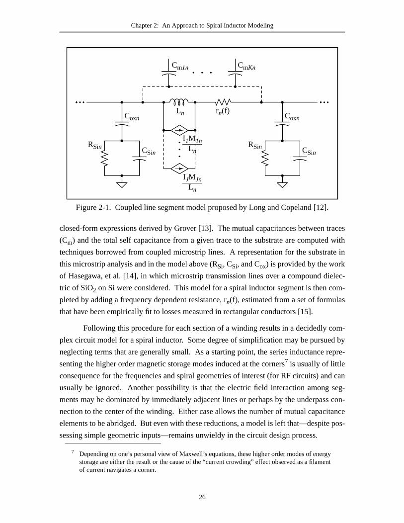
planar spiral is represented by the lumped-elementπ-network shown in Figure 2-1. A
model for anN-turn spiral inductor consists of4N such sections, joined together by
series inductance and shunt capacitance which represent the current crowding eff
each corner of the winding. The self inductance of segmentn within the spiral (denoted
Ln) and the mutual inductances between this conductor and every other segment of th
ral parallel to it (represented by the dependent current sources) are calculated
5 This is, of course, also true for the 3-D solenoid inductors mentioned earlier. Unfortunately,these structures largely remain as curiosities due to having a higher loss per unit inductancecompared to planar spirals and being burdened with a lack of any other particularly redeemingqualities.
6 Good enough? This is a “purposely vague” statement if there ever was one. In this context,good enough might mean that the circuit performance has become limited by something otherthan the inductor (e.g., varactor Q), or perhaps that the inductor loss is already low enough fothe application. Examples of the latter case include DC biasing, emitter degeneration, and evematching networks when some operational bandwidth is desired.
25
Chapter 2: An Approach to Spiral Inductor Modeling
traces
with
te in
lec-
om-
om-
d by
repre-
d can
seg-
s con-
tance
e pos-
ynt
.
closed-form expressions derived by Grover [13]. The mutual capacitances between
(Cm) and the total self capacitance from a given trace to the substrate are computed
techniques borrowed from coupled microstrip lines. A representation for the substra
this microstrip analysis and in the model above (RSi, CSi, and Cox) is provided by the work
of Hasegawa, et al. [14], in which microstrip transmission lines over a compound die
tric of SiO2 on Si were considered. This model for a spiral inductor segment is then c
pleted by adding a frequency dependent resistance, rn(f), estimated from a set of formulas
that have been empirically fit to losses measured in rectangular conductors [15].
Following this procedure for each section of a winding results in a decidedly c
plex circuit model for a spiral inductor. Some degree of simplification may be pursue
neglecting terms that are generally small. As a starting point, the series inductance
senting the higher order magnetic storage modes induced at the corners7 is usually of little
consequence for the frequencies and spiral geometries of interest (for RF circuits) an
usually be ignored. Another possibility is that the electric field interaction among
ments may be dominated by immediately adjacent lines or perhaps by the underpas
nection to the center of the winding. Either case allows the number of mutual capaci
elements to be abridged. But even with these reductions, a model is left that—despit
sessing simple geometric inputs—remains unwieldy in the circuit design process.
7 Depending on one’s personal view of Maxwell’s equations, these higher order modes of energstorage are either the result or the cause of the “current crowding” effect observed as a filameof current navigates a corner.
Figure 2-1. Coupled line segment model proposed by Long and Copeland [12]
rn(f)Ln
Cm1n CmKn
I1M1nLn
IJMJnLn
Coxn
CSinRSin
Coxn
CSinRSin
26

Chapter 2: An Approach to Spiral Inductor Modeling
thors
mpact
pre-
all of
th the
g the
al esti-
more
sitates
ment.
s is
or a
ture
eristics.
rd
.
Irrespective of whether these simplifying assumptions can be made, the au
suggest collapsing the resulting concatenation of line segments and corners into a co
circuit model for the purposes of simulation and optimization. A typical compact re
sentation for an inductor integrated on a silicon substrate8 is exhibited in Figure 2-2, and is
similar to that used by Long and Copeland for each segment of a spiral except that
the intersegment coupling terms are folded into one inductance (lumped together wi
self inductance) and one capacitance (appearing as the shunt element Cs). An approxi-
mate equivalent circuit based on this network can be fit to the complete model, takin
sums of the individual inductances, resistances, and substrate capacitances as initi
mates in the procedure. While this numerical fit does produce a representation
amenable to rapid calculation, any subsequent change in the inductor design neces
another modeling iteration beginning with the parameter calculations for each seg
This is an unfortunate circumstance in that the optimization of circuits with inductor
itself frequently iterative in nature; trading away some thoroughness in modeling f
simpler procedure may thus be considered a potentially worthwhile exchange.
An alternative modeling paradigm is to consider the entire spiral inductor struc
and attempt to reason the first-order dependencies that capture its essential charact
8 The shunt legs of theπ-network representing the substrate make this model specific to the sili-con medium. A model for an inductor on a semi-insulating substrate would drop the oxidecapacitance term. In addition, the high resistivity of materials such as GaAs and InP makes fonegligibly large equivalent substrate resistors, leaving only a capacitance to ground at either enof the network.
CSi1
Cox1
RSi1 CSi2
Cox2
RSi2
Cs
L Rs
Figure 2-2. Compact lumped-element model for an inductor on a silicon substrate
27

Chapter 2: An Approach to Spiral Inductor Modeling
mi-
repre-
y Yue
nd the
ics are
n
en-
ribing
-
ries
cts of
e the
ithin
adja-
a-
typical
ni-
lent
e-
The hope is that this “big picture” approach can yield sufficient accuracy while eli
nating computational steps between the spiral geometry data and a compact model
sentation by focusing on the relevant parasitic effects. A physical model proposed b
and Wong [16] adheres to this methodology. In this work the inductance9 is considered
laden with three dominant parasitics: series resistance, underpass capacitance, a
effect of the substrate. With the one added assumption that the substrate parasit
equally distributed (e.g., Cox1=Cox2=Cox), the corresponding circuit network is that show
previously in Figure 2-2.
Achieving scalability through physics-based formulations for each of the m
tioned effects is a key element in this work. Taken as geometric parameters in desc
the spiral are the width of the conductor that forms the winding (w), the total length of this
conductor (l), the number of turns in the winding (N), and the width of the underpass con
ductor (wup) employed to reach the inner terminal of the spiral. The first parasitic, se
resistance, is assumed to originate from the familiarresistivity× length÷areacharacteristic
of imperfect conductors:
, (2.1)
whereteff represents the effective conductor thickness and is used to model the effe
eddy currents within the conductor. Two sources of these currents—which oppos
applied RF signal—are discussed by Yue and Wong: self induction (from currents w
the same trace, also known as the skin effect) and induction via currents flowing in
cent traces (proximity effect).10 Enlisting the aid of an electromagnetic field solver to an
lyze some representative cases, the authors propose that, at 1GHz and given
dimensions11 for interconnect metallization, proximity effects are not significant for u
planar spirals. Considering then the current distribution in a microstrip line, an equiva
conductor thickness can be derived for use in Equation 2.1:
. (2.2)
9 Most of the modeling effort by Yue and Wong, and all of the discussion pertaining to it whichfollows, concentrates on the parasitic elements in the spiral model. For the inductance itself, thauthors relied upon the Greenhouse method [18], about which more will be said within the context of alternative inductance formulations in Section 2.2.1.
10 Ah, the joys Faraday has brought to light. Time-varying magnetic fields induce electric fields inany material (notwithstanding idealized conductors) through which they pass. Eddy currentsthus also flow in the substrate, another mechanism by which Rs can increase.
11 Metal traces with a 20µm width and 2µm spacing were simulated. To represent the materialsinvolved, 1µm Al metal layers were chosen with an interlevel dielectric consisting of 1µm SiO2.
Rsρl
wteff------------=
teff f( ) δ f( ) 1 et δ f( )⁄–
–[ ]=
28
Chapter 2: An Approach to Spiral Inductor Modeling
yer
tive
eciably
itive
the
ch pair
terms
s, and
l plate
”—
cess
ng an
r the
s this,
r in
wed
e, and
( ).
e split
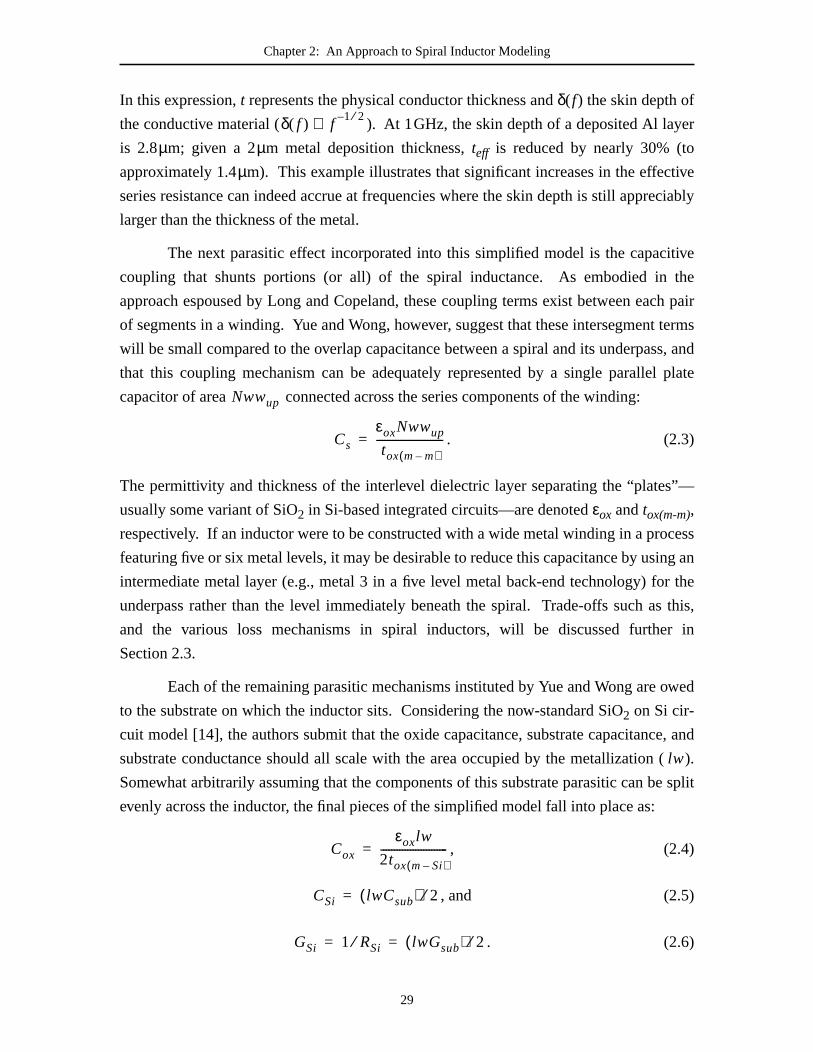
In this expression,t represents the physical conductor thickness andδ(f) the skin depth of
the conductive material ( ). At 1GHz, the skin depth of a deposited Al la
is 2.8µm; given a 2µm metal deposition thickness,teff is reduced by nearly 30% (to
approximately 1.4µm). This example illustrates that significant increases in the effec
series resistance can indeed accrue at frequencies where the skin depth is still appr
larger than the thickness of the metal.
The next parasitic effect incorporated into this simplified model is the capac
coupling that shunts portions (or all) of the spiral inductance. As embodied in
approach espoused by Long and Copeland, these coupling terms exist between ea
of segments in a winding. Yue and Wong, however, suggest that these intersegment
will be small compared to the overlap capacitance between a spiral and its underpas
that this coupling mechanism can be adequately represented by a single paralle
capacitor of area connected across the series components of the winding:
. (2.3)
The permittivity and thickness of the interlevel dielectric layer separating the “plates
usually some variant of SiO2 in Si-based integrated circuits—are denotedεox andtox(m-m),
respectively. If an inductor were to be constructed with a wide metal winding in a pro
featuring five or six metal levels, it may be desirable to reduce this capacitance by usi
intermediate metal layer (e.g., metal 3 in a five level metal back-end technology) fo
underpass rather than the level immediately beneath the spiral. Trade-offs such a
and the various loss mechanisms in spiral inductors, will be discussed furthe
Section 2.3.
Each of the remaining parasitic mechanisms instituted by Yue and Wong are o
to the substrate on which the inductor sits. Considering the now-standard SiO2 on Si cir-
cuit model [14], the authors submit that the oxide capacitance, substrate capacitanc
substrate conductance should all scale with the area occupied by the metallization
Somewhat arbitrarily assuming that the components of this substrate parasitic can b
evenly across the inductor, the final pieces of the simplified model fall into place as:
, (2.4)
, and (2.5)
. (2.6)
δ f( ) f1– 2⁄∝
Nwwup
Cs
εoxNwwup
tox m m–( )-------------------------=
lw
Cox
εoxlw
2tox m Si–( )-------------------------=
CSi lwCsub( ) 2⁄=
GSi 1 RSi⁄ lwGsub( ) 2⁄= =
29

Chapter 2: An Approach to Spiral Inductor Modeling
or the
rms.
eters,
e ele-
f the
ts to
nal
has
the
and
ly-
ding
2-D
lysis
on.
on-
This
ther
to a
s can
ular
d by
s the
road
ult to
tance
rable
erein
Analogous to the formulation for the spiral to underpass capacitance,εox and tox(m-Si)
characterize the dielectric between the winding and the surface of the Si substrate. F
substrate itself,CsubandGsubrepresent (per unit) area capacitance and conductance te
Though physical in nature, these terms may essentially be treated as fitting param
established empirically through data on measured spirals. This collection of substrat
ments completes a simplified yet promising picture of spiral inductors consisting o
most significant parasitic effects and constructed with models that relate the effec
geometry. While this model forms an excellent starting point, a couple of additio
developments may offer improvements; these are discussed in Section 2.2.1.
A third tact toward addressing the problem of modeling spiral inductors that
been investigated is the construction of an electromagnetic field solver simplified to
extent possible for handling this one specific case. One such effort by Niknejad
Meyer has resulted in ASITIC12 [17], a tool that combines a set of more computational
efficient techniques that has been developed for solving EM fields around a metal win
on a multi-layered substrate, with a graphical interface for conveniently generating
spiral layouts of interest. Although the simplifications do appreciably reduce ana
times, the simulations are still too lengthy to provide for efficient inductor optimizati
In fact, the procedure used in ASITIC for optimizing a geometry to meet design c
straints still relies upon a collection of approximate lumped-element solutions.
results in a point along the simplicity-accuracy design trade-off that is similar to the o
modeling approaches that have been presented.
2.2.1 Alternative Inductance and Series Resistance Formulations
The “divide and conquer” inductor models just described segment the spiral in
conjoined set of straight-line sections for which the self and mutual inductance term
be calculated (for each section) using Grover’s closed-form expressions for rectang13
conductors [13]. The total inductance realized by the spiral can then be compute
summing over all the sections comprising it, a technique generally referred to a
Greenhouse method [18]. While known to yield usable results over a reasonably b
range of geometries, this method is somewhat labor intensive, and becomes diffic
apply to non-rectangular spirals; an expression that could directly provide the induc
with comparable accuracy from simple geometric parameters would be a prefe
solution. Several such expressions have been proffered by Mohan, et al. [19], wh
12 Named more for what it’s used rather than for what it is, ASITIC originates from Analysis andSimulation of Inductors and Transformers for Integrated Circuits [17].
13 Here, “rectangular” refers to both the cross-sectional shape of the conductor and the layout.
30

Chapter 2: An Approach to Spiral Inductor Modeling
enta-
piral
solver
m
ed
-
t sheet
heets
ce
h of
ounts
1.
-
s
[19]
some quasi-physical formulas have been fit to the EM simulation results for a repres
tive library of planar spiral inductors. A comparison against measured data for 60 s
structures demonstrates that the reported expressions perform as well as the field
offered in ASITIC,14 typically yielding inductances within 5% of those extracted fro
measurements.15
Defining the outermost dimension of a spiral geometry asdout and the innermost as
din, the inductance of a spiral can be characterized by the number of turns (N), the average
diameter , and the fill ratio of the spiral, where the latter is defin
as . The second form of the fill ratio expres
sion recalls an approximation where each side of a spiral is represented as a curren
of width Wsh, while the length of the sheets and the separation between opposing s
are both characterized by the distancedavg. This gives rise to a geometric mean distan
formulation for the total inductance of the spiral:
, (2.7)
which is at least mildly satisfying in that the inductance is proportional to: the lengt
the conductor, the square of the number of turns, and a multiplicative factor that acc
for the mutual coupling from opposite sides of the spiral. The constantsci are fitting
parameters dependent upon the shape of the spiral, and are listed below in Table 2.
14 The correspondence here is not terribly surprising as the data points to which the expressionswere fit were generated by the same EM field solver. What is of note, however, is that a rela-tively low-order model (represented by the inductance expressions) can represent with reasonable accuracy a range of spiral inductors likely to be useful in integrated circuits.
15 One observation on the error analysis offered by the authors is that thesmallest inductanceamong the measured test set is 2.5nH, and that the three inductors of less than 3nH availed adata points are associated with the largest relative errors listed in the experiment. In designsintended to operate at frequencies much above a few gigahertz, the inductances will generallyfall below the range spanned by the comparison set.
Table 2.1: Fitting Parameters for GMD Inductance Formulation, from Mohan, et al.
Spiral shape c1 c2 c3 c4
Square 1.27 2.07 0.18 0.13
Hexagon 1.09 2.23 0.00 0.17
Octagon 1.07 2.29 0.00 0.19
Circle 1.00 2.46 0.00 0.20
davg dout din+( ) 2⁄=
ρ dout din–( ) dout din+( )⁄ Wsh davg⁄= =
Lµ0N
2davgc1
2-----------------------------
c2
ρ-----
ln c3ρ c4ρ2+ +
=
31

Chapter 2: An Approach to Spiral Inductor Modeling
the
fre-
aking
ave a
elec-
three
mag-
n wit-
ined.
iral
me-
ag-
ner
al to
uced
a fre-
e.
mes
the
ing,
ate of
n
Another component of spiral inductors that warrants further consideration is
series resistance imposed by the winding and the manner in which it may vary with
quency. The models discussed earlier in this chapter consider only the skin effect, m
the assumption that the various coupling mechanisms within the inductor structure h
negligible effect on the resistance. Yue and Wong explored this assumption through
tromagnetic simulations of coupled line segments [16], but their representation of
adjacent traces does not necessarily correspond to that of a spiral inductor where the
netic flux passing through the center of the spiral can have a much higher density tha
nessed around the periphery of the spiral where the fields are not so tightly constra
As a result, current crowding will first be observed in the inner-most turn of a sp
winding, an asymmetry not captured in the preceding analyses.
By examining the electromagnetic simulation results for a range of spiral geo
tries, Kuhn and Ibrahim [20] propose that a more representative distribution of the m
netic fields impinging upon the winding is that the intensity is at a maximum at the in
turn and then decreases linearly turn-by-turn. Considering the magnetic field norm
the winding and averaged (in magnitude) over the inner turn, the magnitude of the ind
eddy current in this turn becomes equal to that of the applied RF excitation current at
quency characterized by:
, (2.8)
where the spiral geometry is captured by the turn pitch (p) and the width of the metal
winding (w), while Rsheetdenotes the sheet resistivity of the metal in Ohms per squar16
Noting that, for most spirals, the metal spacing is much smaller than the width, it beco
evident that proximity effects gain significance at frequencies inversely proportional to
width of the trace used to form the inductor.
Next, formulating the power dissipated by the eddy currents within the wind
the authors use the characteristic frequency in Equation 2.8 to provide a rough estim
the effective series resistance of the spiral in terms of its DC resistance (RDC):
. (2.9)
16 While the factor of 3.1 in the numerator of Equation 2.8 may look tantalizingly close toπ, this infact is little more than a fitting parameter resulting from an observation made by the authors (ithe EM simulations) that the magnetic flux density normal to the inner-most turn of the spiralcan be approximated as over a fairly wide range of geometries.
ωcrit3.1p
µ0w2
------------Rsheet=
BN µ0I 1.54p( )⁄=
Reff RDC 1110------ ω
ωcrit-----------
2+≈
32

Chapter 2: An Approach to Spiral Inductor Modeling
of the
more
ition
ency
-
g fre-
nd
ratic
at the
er of
ing
epen-
same
son to
diffi-
ell
ns are
ns,
ation
ated
dia-
e is
ding
y
r loss
y (as
more
d sig-
. At
This quadratic increase with frequency eventually stalls, however, as the presence
eddy currents counters the magnetic field that was initially assumed, resulting in a
linear relationship at higher frequencies. Kuhn and Ibrahim submit that the trans
between the quadratic and linear regimes of current crowding will occur at a frequ
roughly a factor of 4 to 6 beyondωcrit. Though this limits its range of validity, the approx
imate expression for effective resistance (Equation 2.9) does catch some interestin
quencies in the low gigahertz RFIC design space. Calculating for the cases of 1µm thick
aluminum in widths of 10µm and 20µm, the corresponding critical frequencies are fou
to be 1.2GHz and 600MHz, respectively. Hence a region of resistive behavior quad
in frequency up to 2-3GHz might be expected in typical spiral inductor applications.
It can be witnessed in these examples and the preceding relationships th
proximity effect does not depend on either the size of the inductance or the numb
turns in the spiral, but rather just the width of the conductor and its resistivity. Be
induced by the same magnetic field-based mechanism, the skin effect is similarly ind
dent of the spiral geometry, and also begins to play a role in inductor loss over the
frequency ranges discussed in the context of current crowding. Perhaps the best les
be taken from this work is that the frequency-dependent nature of conductor loss is a
cult modeling challenge and, as a result, any simplified model is likely to only work w
in a restricted range of frequencies and geometries. Some first-order consideratio
captured by the models presented here which allow for optimization within limitatio
but a final-stage spiral design should still be submitted to an electromagnetic simul
tool when inductor loss is of critical importance.
2.3 Spiral Inductor Loss Mechanisms
If there is anything that can be considered an absolute certainty with integr
inductors, it is that the devices will fall short of their lossless ideal. A cross-sectional
gram of a spiral inductor sitting on an insulating layer covering a silicon substrat
shown in Figure 2-3, where an external signal has been applied to the metal win
which in turn carries the signal currentI. Some of the signal energy will be dissipated b
resistance encountered in the winding, and is generally the dominant spiral inducto
mode at low frequencies. While the resistance will effectively increase with frequenc
discussed in the preceding section), other loss mechanisms will begin to play even
significant roles at higher frequencies. First, the potential associated with the applie
nal creates an electric field for which the substrate is essentially an RF termination
33

Chapter 2: An Approach to Spiral Inductor Modeling
le to
face
can
rate as
nd the
onent
term
y and
[14].
[21],
ave
g in
e field
bstrate
al.
trate)
rans-
t
lower frequencies—in typical silicon material—charge carriers in the substrate are ab
respond and “follow” the electric field, and the field thus terminates at the inter
between the oxide and the silicon.17 As the signal rates increase, however, the carriers
no longer keep pace, and the electric field subsequently penetrates into the subst
sketched above in Figure 2-3. When the charges move in response to, but lag behi
applied field, the resultant (capacitive) current contains a real (i.e. in-phase) comp
that can be modeled by an insulator having a dielectric constant with an imaginary
that is frequency dependent. A capacitor constructed from such an insulator is loss
can be represented in circuit form by the addition of a parallel substrate resistance
While potentially addressable through the incorporation of patterned ground shields
this capacitive loss mechanism begins to limit inductor quality at moderate RF/microw
frequencies.18
A third effect is that the magnetic field generated by the signal current flowin
the spiral also penetrates into the substrate. Analogous to a transformer where th
generated by one winding passes through another, a current is induced in the su
(shown in Figure 2-3 asI2) flowing in the direction opposite that of the intended sign
Continuing the transformer analogy, this eddy current flows in the secondary (subs
side as a result of signal energy applied to the primary winding and, just as with a t
17 This behavior is why the lumped oxide capacitance approximation, typically accepted withoutquestion by IC designers, works at all. Without an explicit conductor or other source of carriers(e.g., a MOSFET source/drain region) present beneath the oxide, this approximation becomesdubious at gigahertz frequencies in lightly doped (e.g., 10-20Ω-cm) silicon, and even earlierwhen more heavily doped wafers are used.
18 And yes, this is another purposely vague description. Generally this effect becomes prominenin the neighborhood of a few gigahertz, although the location of the “neighborhood” depends onthe area occupied by the spiral, oxide thickness, and substrate resistivity. More regarding thistopic can be found in the paper by Hasegawa, et al., which analyzed SiO2 on Si microstrip [14].
Figure 2-3. Loss mechanisms in a spiral inductor.
Si
SiO2
Al, AlCu, or Cu
I
I
I2I2ε
34

Chapter 2: An Approach to Spiral Inductor Modeling
n be
, this
al for
uality
t only
t fun-
unding
e
ilarly
e
lves
nergy
ments
urce;
dissi-
athe-
that
ality
d the
former, loss encountered in the “secondary” due to finite substrate resistivity ca
observed through the primary side. At higher RF and microwave design frequencies
becomes a very significant loss term in silicon-based spiral inductors.
2.3.1 Inductor Quality Factor
Enough has been written in this chapter alone to be suggestive of the potenti
inductor loss, but some means of quantifying the loss is needed. The concept of a q
factor, a ratio between stored and dissipated energies within an element, proves no
enlightening but also quite useful for design and optimization. Despite the apparen
damental energy-based origins, however, there remains considerable debate surro
the definition of quality factor (often called simply just “Q”). Invariably, some of th
questions being debated pertain to application-specific contexts, although a sim
enthusiastic discussion can be found regardingwhichmeasure of stored energy should b
used in the assessment of quality factors.
For the case of an inductor, the most conventionally-used definition of Q invo
the energy that an external source is able to store in the inductance divided by the e
dissipated in the device. Under this interpretation, the electrical energy storage ele
(capacitors) associated with the inductor effectively compete against the external so
at the self-resonant frequency, the only energy taken from the source will be that
pated by the loss mechanisms in the inductor, and hence the Q will be zero. Stated m
matically, this involves a subtraction of the peak energy stored in electrical form from
in the magnetic fields of the inductor [22]:
. (2.10)
Given this formulation and the lumped-element model shown in Figure 2-2, the qu
factor of a spiral inductor can be calculated as:19
, (2.11)
where the series inductor components are grouped together as an
effective time constant associated with the substrate parasitic elements is denoted:
19 For the truly curious, an element-by-element derivation is provided in the Appendix.
Q 2π Peak Magnetic Energy Peak Electrical Energy–Energy Loss in One Oscillation Period
----------------------------------------------------------------------------------------------------------------------≡
Q
ω L
Zs2
------ Cs– Cox 1 sτsub–( )2– CSi sτsub( )2
–
Rs
Zs2
------sτsub( )2
RSi-------------------+
----------------------------------------------------------------------------------------------------------=
Zs Rs jωL+=
35

Chapter 2: An Approach to Spiral Inductor Modeling
nship
. But
ting
-used
e
arity
ality
tion
tor is
nduc-
quiva-
. At
ing in
eed
ar to
f its
fac-
order
ectly
th. A
ccom-
ctor at
en a
ctice
ber
. (2.12)
Equation 2.11 can be observed to collapse to at low frequencies, the relatio
expected in a simple model of an inductor having only a series resistor loss element
more generally, this definition is also consistent with the approach of directly calcula
quality factors from measured small-signal parameters, being equivalent to the oft
forms and [23].20 This correspondence, and th
convenience it affords, undoubtedly is a significant contributor to the continued popul
of this manifestation of Q.
Unfortunately, a shade of murkiness begins to be cast over this picture of qu
factor in noting the many circuit applications which introduce capacitance in conjunc
with an inductor. It can be argued, for example, that the Q associated with a resona
not accurately reflected when the above definition is used to describe a constituent i
tance. Consider first the extreme case of an inductor used at self-resonance, or e
lently, lowering the resonant frequency of the inductor by adding an ideal capacitor
resonance, the electrical and magnetic energy storage forms will balance, result
for the inductor via Equation 2.11. It is evident, however, that energy is ind
being stored in the resonator, which should therefore have ; this would appe
violate the intuitive notion that the Q of the whole should not exceed the Q of any o
parts.21
One way out of this quagmire is to use bandwidth-based definitions for quality
tor, provided that the circuit networks under consideration are approximately second-
and that the loss is not prohibitively high. For a resonator, Q can be observed dir
from the frequency response as the ratio of the center frequency to the 3dB bandwid
consistent approach for an inductor makes use of the same definition, and can be a
modated by the addition of (lossless) capacitance as required to resonate the indu
the frequency of interest—a manipulation that can be performed mathematically giv
two-port characterization of the inductor. For further discussion regarding the pra
and pitfalls in quality factors, the reader is referred to a paper by O [24] in which a num
of Q metrics are analyzed and compared across some measured inductors.
20 For the equivalence to hold, the inductor must effectively be connected in a one-port config-uration (i.e. having one of the inductor terminals grounded). Regardless of the physical con-nection, using the short-circuit admittance (y) parameters enforces this. However,unless the second terminal is physically a small-signal ground.
21 The most satisfying relationship for an LC tank would be , whereQL andQC denote the individual quality factors for the inductor and capacitor.
τsub
RSiCox
1 sRSi Cox CSi+( )+------------------------------------------------=
ωL Rs⁄
Im– y11 Re y11 ⁄ Im z11 Re z11 ⁄
z11 1 y11⁄≠
Q 0=
Q 0>
1 Q⁄ 1 QL⁄ 1 QC⁄+=
36

Chapter 2: An Approach to Spiral Inductor Modeling
qual-
ion-
l gen-
sitics
d in
duc-
Q are
e dif-
to be
tors,
ss as
. As
etric
ls are
ithin
or a
is not
ion of
ling
hout
et for-
para-
d by
a) are
rk of
-
It would seem then that there is no easy answer to be found in the debate over
ity factor definitions, in that the most appropriate description will always be applicat
dependent. For an oscillator circuit, Q values based on bandwidth considerations wil
erally be more relevant, although the calculations should incorporate transistor para
associated with the oscillator itself in addition to any output loading.22 Conversely, when
inductive behavior is desired for tuning or stabilizing a gain stage, the metric define
Equation 2.10 is likely to be of greater consequence. Pragmatically though, for in
tances smaller than a few nanohenries, differences among the various definitions of
not large—in either the value or the frequency at which the value peaks. While thes
ferences should not be dismissed as insignificant, design decisions are not likely
appreciably impacted by the working definition chosen for quality factor.
2.4 Quick Turn Models for Spiral Inductors
Earlier sections in this chapter have discussed typical applications of induc
investigated a few efforts geared toward providing models of them, and explored lo
one of the predominant concerns encountered in using integrated inductances
intimated earlier, however, a means of rapidly generating circuit models from geom
descriptions is required to enable the design of circuits using inductors. The mode
used for both circuit simulation and also for balancing the various loss mechanisms w
the inductor itself—by scaling the geometry—to optimize a chosen metric (e.g., Q f
given inductance) over a desired range of frequencies. The purpose of what follows
to propose any ground-breaking modeling advances, but rather to describe a collect
approximate tools which work well together and provide a convenient rapid mode
capability.
For the spiral inductors used in conjunction with the circuits presented throug
this thesis, a first-pass calculation of the inductance is obtained from the current she
mulation tendered by Mohan, et al., and presented in Equation 2.7. The associated
sitic elements are computed following the approach of Yue and Wong as describe
Equations 2.1 through 2.6. Unit capacitance and conductance terms (i.e. per unit are
required in this approach for modeling the substrate, and the microstrip on silicon wo
Hasegawa, et al. [14] is tapped to derive these components. Lightly-doped23 substrates
22 This is sometimes called the “loaded” Q of the resonator, even when the only loading is fromtransistor parasitic elements. Maximizing loaded Q for an oscillator can be an important consideration in sizing the inductive portion of a resonant tank.
23 Silicon substrates used for RFIC applications are typically p- material in the 10-20Ω-cm range.
37

Chapter 2: An Approach to Spiral Inductor Modeling
een a
strate
tor
for Q
or its
that
Once
es are
istance
on-
l
d
sured
te
e
r
e
support a mode of propagation at RF frequencies that is transitional in nature betw
slow-wave mode and a more familiar quasi-TEM arrangement,24 a behavior that is mod-
eled by an oxide capacitance ( ), a substrate capacitance ( ), and a sub
conductance ( ).25 Finally, to allow comparisons across candidate spiral induc
structures, the loss corresponding to each spiral is quantified using the relationship
established in Equation 2.11; this particular quality factor metric was chosen largely f
ease of calculation. These equations have been coded into a MATLAB [25] routine so
a suite of lumped-element model component values (L, Rs, Cs, Cox, CSi, andRSi) can at
once be generated for a list of inductors specified by a set of geometric parameters.
the optimal geometry has been identified from the model data, FastHenry [26] analys
performed on the chosen spiral structure to more accurately determine the series res
and inductance at the frequency of interest.
While the implementation of this approach is relatively straight-forward, one n
trivial aspect is determining the total length (l) of the metal traces comprising the spira
(required in the expressions forRs, Cox, CSi, andRSi). For the purposes of this model, an
as indicated by the dashed line in Figure 2-4, the length of the spiral should be mea
24 The difference in the propagation modes pertains to the behavior of the carriers in the substrain response to the electric field impressed by the applied signal. A quasi-TEM mode predomi-nates at higher frequencies, when the carriers in the substrate are no longer able to respondquickly enough to charge and discharge the oxide capacitance. Conversely, the slow-wave modis characterized by a movement of charge at the substrate-oxide interface in response to thetime-variant electromagnetic fields. The latter mode results in a higher effective capacitance peunit length of (microstrip) trace, resulting in a lower propagation velocity.
25 Each of these per unit area terms can be modified to account for the fringing effects (i.e. widthdependence) prevalent when the trace width is much smaller than the substrate thickness. Thclassical microstrip treatments can also be applied to this multiple dielectric case.
εox tox⁄ εSi tSi⁄σSi tSi⁄
dout din
Figure 2-4. Geometry parameters describing a square spiral inductor.
llast
l first
38
Chapter 2: An Approach to Spiral Inductor Modeling
seg-
e
g the
d for
d for
more
ed with
.13, or
series
ius that
ay be
he
t not
loss
ms.
ffects
rele-
along its center line. Considering the geometry of a square spiral havingN turns, an outer
dimensiondout, metal widthw and spacings, the length can be expressed as:
, (2.13)
where the lengths of the first segment of the spiral and the last
ment are indicated separately. Inserting th
expressions for the first and last segments, evaluating the summation, and simplifyin
result, the length of metal comprising a square spiral can then be quickly determine
an integer number of turns:
. (2.14)
The quick-turn spiral inductor model described above can essentially be use
arbitrary shapes, although inductance fitting coefficients are only available for the
commonly encountered squares, hexagons, octagons, and circles. Lengths associat
hexagonal and octagonal inductors can be addressed through variants of Equation 2
by approximating the shapes as being circular for the purposes of calculating the
resistance and substrate parameters. True circular spirals are characterized by a rad
decreases toward the center at a fixed angular rate; the length of a circular spiral m
posed in terms of its initial radius (ri) and final radius (rf) as:
, (2.15)
assuming . Noting that , and performing the integration, t
length of trace comprising a circular spiral is also seen to be readily determined:
. (2.16)
This completes a study of spiral inductors that has been geared toward—bu
limited to—use in silicon-based integrated circuits. The silicon medium introduces
and additional modeling complexity into a device already rife with coupling mechanis
But a number of recently-advanced treatments handle many of the most significant e
in terms of geometric dependencies, yielding some hope that inductors need not be
gated to the design by trial-and-error scrap heap.
l l first 2 dout w– k w s+( )–[ ]k 0=
2 N 1–( )
∑
l last+ +=
l first dout w 2⁄–=
l last dout w 2⁄– 2N 1–( ) w s+( )–=
l dout 4N 1–( ) dout w–( )+ 2N 1–( )2w s+( )–=
l r i
r i r f–
2πN---------------
θ– θd
0
2πN
∫=
r i r f> r f r i N w s+( )–=
l πN 2r i N w s+( )–[ ]=
39

Chapter 2: An Approach to Spiral Inductor Modeling
g to
rectly
del
) of
n
the
Appendix: Calculation of Inductor Quality Factor
While quality factors can be derived from measured data, it is also satisfyin
know that the energy-based perspective of Q provided by Equation 2.10 can be di
applied to a circuit model of an inductor. Grounding one port of the spiral inductor mo
and driving the other with a sinusoidal voltage source (y-parameter configuration
amplitudeV1, the circuit to analyze appears as shown below.
In response to the applied voltage, the peak current flowing in the inductor will be:
, (2.17)
and thus the maximum energy stored in the inductance is:
. (2.18)
The same current flows in the resistance Rs, prompting an energy loss per oscillatio
period ( ) as given by:
, (2.19)
where the factor of one-half is needed to get the RMS value of the current. If all of
capacitances in the circuit were negligible, the inductor quality factor would then be:
CSi
Cox
RSi
Cs
L Rs
V1sinωt
Figure 2-5. Circuit model for calculation of inductor quality factor.
iV1
Rs jωL+----------------------=
WL12---Li
2 L2---
V12
Rs jωL+( )2------------------------------==
ω 2π⁄
WR Rsi2
2---- 2π
ω------
Rs
2-----
V12
Rs jωL+( )2------------------------------ 2π
ω------
==
40

Chapter 2: An Approach to Spiral Inductor Modeling
naly-
to the
te RC
s
e
ted
n
, (2.20)
as expected and as observed at low frequencies.
Unfortunately, the capacitances all too often cannot be neglected, and so the a
sis and subsequent expressions for Q become more complex. The voltage applied
circuit also falls across the shunt capacitance Cs, imparting a peak energy:
. (2.21)
The substrate network divides the applied signal, with the voltage across the substra
being given by:
, (2.22)
with τsub being introduced to simplify later expressions.26 Summing the peak energie
stored in the oxide and substrate capacitances yields:
, (2.23)
completing the litany of energy storage terms. Finally,VSi is also impressed across th
substrate resistance RSi, dissipating an energy per period:
, (2.24)
making the total loss per period in the inductor:
, (2.25)
where is used for further simplification. Quality factor is then construc
with the capacitive energy terms subtracting fromWL, matching the expression show
earlier in Equation 2.11:
. (2.26)
26 It will be well worth the extra notational confusion!
Q 2πWL
WR------- ωL
Rs-------==
WCs
12---CsV1
2=
VSi
sRSiCox
1 sRSi Cox CSi+( )+------------------------------------------------V1 sτsubV1==
WCsub
12---CoxV1
21 sτsub–( )2 1
2---CSiV1
2sτsub( )2
+=
WRSi
V12
2RSi----------- sτsub( )2 2π
ω------
=
Wloss WRsWRSi
+2πω------
V12
2------
Rs
Zs2
------sτsub( )2
RSi-------------------+
= =
Zs Rs jωL+=
Q 2πWL WCs
WCsub+( )–
Wloss----------------------------------------------=
ω L
Zs2
------ Cs– Cox 1 sτsub–( )2– CSi sτsub( )2
–
Rs
Zs2
------sτsub( )2
RSi-------------------+
----------------------------------------------------------------------------------------------------------=
41

Chapter 2: An Approach to Spiral Inductor Modeling
42

fiers
mix-
can be
ons.
g RF
com-
euris-
al as
ional-
cuit
er-
that a
f them
n
ends
hin
t input
that
it that
l.
Chapter 3
Time-Variant System Modeling
Together with a collection of passive elements, oscillators, mixers, and ampli
form the canonical infrastructure of RF and microwave transceivers. Oscillators and
ers are central to the frequency translation and synthesis processes, and amplifiers
targeted for low noise, power, intermediate frequency, and signal-limiting applicati
Understanding the manifestation of noise in these circuits is essential for extendin
system performance while reducing the costs of development. Where the front-end
ponents were once considered largely within the province of design-by-experience h
tic approaches, greater sophistication in the modeling is becoming increasingly vit
technological limitations are pushed by demands for increased bandwidth and funct
ity in wireless systems.
Two important distinctions that can be drawn with respect to modeling any cir
pertain to linearity and time-invariance. Linearity is defined by the principle of sup
position—perhaps one of the greatest friends of engineers everywhere—and implies
system yields the same behavior regardless of the size of the signals or the number o
that are applied. Stated more formally, if a system responds with an outputy1(t) when
subjected to an inputx1(t), and similarly generatesy2(t) given a different inputx2(t), then a
composite and scaled input will result in an output whe
applied to the same system if it is linear. Time-invariance is another property that l
itself to simplification, implying that there is no inherent context of absolute time wit
the system. A given input signal generates the same output irrespective of when tha
is applied. Framed within a fixed time reference, if the inputx1(t) is delayed by a timeτ:
x1(t-τ), then the corresponding output is simplyy1(t) delayed by the same interval:y1(t-τ).
The combination of these two qualities results in a linear time-invariant (LTI) system
can be completely characterized by a single impulse response, a greatly beneficial tra
allows the response to an arbitrary input to be determined from a convolution integra1
1 This property also opens the door to all the usual frequency-domain analysis tools.
ax1 t( ) bx2 t( )+ ay1 t( ) by2 t( )+
43

Chapter 3: Time-Variant System Modeling
nsid-
arity
dels
] and
dels
tion,
d pre-
ixers.
-
d to
ircuit.
LTI
at the
ould
has
h at a
arac-
e-
toring
ctory
ses in
and a
Among the active elements in RF transceivers, amplifiers can generally be co
ered LTI over a useful range of inputs, with some measure of the limits to the line
being conveyed through distortion or compression levels. Linear time-invariant mo
have also been used to help cast light upon design trade-offs for oscillators [27]-[29
mixers [30]. Though often yielding intuitively-appealing analogies, the LTI-based mo
of oscillators and mixers fail to catch some fundamental mechanisms of their opera
potentially leading designers astray. This chapter investigates these limitations an
sents an approach for using time-variant models to analyze noise in oscillators and m
3.1 A Plausibility Argument for Time-Variant Models
The first widely-accepted2 framework for considering oscillator noise was ten
dered in the mid-1960s by Leeson [28], wherein a plausible argument was crafte
explain the spectrum observed around the carrier generated by an oscillator c
Instilling slightly more rigor into the framework, Lindenmeier subsequently used an
description to demonstrate that the spectrum primarily consists of phase noise, and th
spectral density arising from a resonant oscillator (excluding flicker noise sources) c
be expected to behave as [29]:
. (3.1)
Although not introduced until well after the initial theories were advanced,
become the commonly-used notation to indicate the noise power in a 1Hz bandwidt
frequency displaced∆f from the carrier, expressed in dB relative to the carrier power (Po),
and with the units usually expressed as dBc/Hz. In Equation 3.1, the oscillator is ch
terized by the quality factor of the resonator (Q) and a multiplicative excess noise param
ter (F) that is used to fit the noise contributions of the circuit.3 This relationship also lends
itself to a satisfying energy-based interpretation: as the energy that can be held in s
the state of the oscillator becomes larger, the susceptibility of the (state-space) traje
to perturbations from noise decreases, subsequently lowering phase noise. Increa
the carrier power are a reflection of having more energy stored in the resonator,
2 This may be an indication that it was the first widely-understood treatise concerning oscillatornoise. Expositions concerning variations in the frequency of oscillation can be traced back tothe 1930s [31].
3 The excess noise parameter was originally conceived to be related to the noise factor of theamplifier stage around which the oscillator was formed, giving rise to its designation asF.
L ∆f 10kTFPo
---------- 1
Q2
------ 1
∆f fo⁄( )2----------------------log=
L ∆f
44

Chapter 3: Time-Variant System Modeling
igher
onding
oise.
hat it
ears.
g the
l LC
erate
oidal
ertur-
but
ulse
tude
The
decay
ferent
effect
e
,
4].
higher Q means that less of it is dissipated during an oscillation cycle. Conversely, h
carrier frequencies necessitate smaller-valued resonant tank elements; the corresp
reduction in energy available to store the oscillator state leads to increased phase n4
Despite the lack of a clear idea as to what the excess noise factor is or on w
depends, Leeson’s model was the predominant view of oscillator noise for about 30 y
More recent developments, however, have illustrated the importance of incorporatin
time-varying behavior exhibited by oscillators. As a demonstration, consider an idea
tank in isolation. Once energy has been introduced into the system, the energy will it
between being stored in the inductor and the capacitor, indefinitely producing a sinus
signal as depicted by the solid traces in Figure 3-1. The dashed lines overlay the p
bation response of the system to two impulsive noise events equal in amplitude
occurring at different locations within the oscillation period. In the first case, an imp
of energy is injected into the LC circuit when the signal is at an extremum. The ampli
of the oscillation responds immediately, but the phase of the signal is unchanged.
dynamics of amplitude restoration essential to oscillators cause the disturbance to
with time, leaving behind no lasting effect to the state of the system.5 However, when the
same noise event is introduced near a zero-crossing in the waveform, a decidedly dif
picture emerges as the phase of the oscillation is offset by the disturbance. While no
4 An alternative view is to consider the resonator as filtering the spectrum of the noise, limiting theeffective noise bandwidth impinging upon the oscillator to . The phase noise ofthe oscillator is then proportional to the power spectral density of the noise and the square of thnoise bandwidth (i.e. ) [32].
5 Some type of amplitude-limiting mechanism is required for a steady-state oscillation to exist[27]. Fortunately, there is such a mechanism inherent to the behavior of many transistor circuitsas gain usually falls with increasing signal swing.
fBW fo Q⁄=
Sφ kTF fBW2∝
Time Time
Osc
illa
tion
am
plit
ud
e
Osc
illa
tion
am
plit
ud
e
Figure 3-1. Pictorial argument for a time-variant oscillator model, adapted from [3
Noise injected atτ=0Noise injected atτ=π/2
45

Chapter 3: Time-Variant System Modeling
echa-
a dif-
nal
e IF
mined
ent
pair,
con-
c-
all.
erval
being
cally
rt of
du-
mple),
y be
oise
upon the signal amplitude is witnessed, oscillator dynamics lack a complementary m
nism to restore phase, and so the disturbance persists.6
As a second example, a single-balanced mixer is shown in Figure 3-2, where
ferential local oscillator (LO) drives the emitter-coupled pair and the incoming RF sig
is coupled to the lower transistor. From the perspective of signal transmission to th
outputs, three different modes of operation are exhibited on a periodic basis as deter
by the applied LO. When is more than a few above , all of the curr
established by the tail transistor passes through the left side of the differential
enabling a cascode amplifier connection between and . Under the opposite
dition ( ), is pulled toward the supply voltage through the colle
tor load and the transmission from the RF input to the positive IF output is very sm
Conversely, the switching core operates in a high differential gain mode during the int
that the LO is between these extremes, with approximately half the RF signal energy
directed toward either output.
Given the three distinct modes evidenced in the signal gain that varies periodi
with the LO, it should come as no surprise that an LTI-based model would fall sho
capturing essential mixer behavior. The time-varying nature of the circuit not only mo
lates the magnitude and effect of each noise source (as observed in the oscillator exa
but also fundamentally underpins the frequency conversion process. While it ma
tempting to try using time-averaged values for gains in the calculation of the mixer n
6 A phase-locked loop (PLL) provides a phase-restorative function for an oscillator, which is whythe phase noise spectrum of an oscillator is attenuated by a PLL.
vLO+ kT q⁄ vLO–
vRF vIF +
vLO– vLO+– ~ 3kT> vIF +
vLO vLO+
vIF+ vIF
vRF+VDC
Figure 3-2. Simplified schematic of a single-balanced mixer.
-
-
46

Chapter 3: Time-Variant System Modeling
ncies
figure
riant
iqui-
n of
ach to
ith a
een
prob-
riodic
icity
tech-
mpli-
35], a
roach
36].
tial
is time
inter-
nse,
in
puted
ee
con-
ying
ared
-
figure, even an ideal switching core aliases noise in the input current from freque
around each LO harmonic to the same IF band, appreciably increasing the noise
above that of the input transconductor. A method of capturing the effects of time-va
behavior is clearly needed to help guide the mixer and oscillator designs that are ub
tous in RF circuits, and to provide greater insight into the selection and optimizatio
semiconductor technologies for these applications. This chapter develops an appro
using time-variant models in the analysis and design of oscillators, and concludes w
discussion of how the same method can be extended to mixers.
3.2 Oscillator Analysis Using a Linear Time-Variant Model
Once the assumption of time-invariance in oscillators and mixers has b
observed to be precarious, the question becomes where to turn next. Fortunately, the
lem is not completely unconstrained, as both types of circuits operate under a pe
steady-state condition; mixers and oscillators may not be time-invariant, but period
limits the scope of the analysis and leaves open the possibility of using Fourier-based
niques. Furthermore, linearity in these RF circuits can be seen to hold for the small a
tudes generated by noise sources and exhibited by most RF and IF signals [33]-[
property that simplifies the task considerably. The use of a periodic time domain app
to analyzing the effects of noise in oscillators was first illustrated by Kärtner in 1990 [
Kärtner introduced the application of perturbation methods for solving the differen
state-space equations which represent the behavior of an oscillator and noted at th
that linearity should persist. However, the presentation in this section is based on an
pretation first offered by Hajimiri and Lee [38].
A linear time-variant (LTV) system can be characterized by an impulse respo
albeit one that is time-varying. While its calculation is often bypassed for LTI circuits
favor of frequency-domain approaches, an impulse response can be directly com
with the aid of any circuit simulator. Following the development by Hajimiri and L
[34], an oscillator is first subjected to a transient analysis run until the steady-state
dition is reached. An impulse of energy is then introduced into the oscillator by appl
a narrow pulse7 from a current source, and the output signal that results is comp
7 When an input signal is much shorter in duration than the response time of the circuit to which itis applied, the circuit does not respond to the shape of the input but rather just the energy contained within it. A discrete Fourier transform (DFT) of the signal approximating an impulse canbe used to validate this criterion. The transform of an impulse is a constant, and the DFT of thepulse used in simulations should closely approximate this through the frequencies of interest.
47

Chapter 3: Time-Variant System Modeling
pro-
rcuit
of the
thus
extent
orre-
scil-
ero-
against the undisturbed oscillation to gauge the impulse response of the circuit. This
cedure is depicted schematically in Figure 3-3(a-c).
The impulse of charge introduced by the current source deposits onto ci
capacitances that store the state of the oscillator, instantaneously changing the value
voltage state variable. Continuing surreptitiously from this new state, the oscillation
withstands a step in phase; the change in phase can be calculated by measuring the
to which the zero-crossing points in the output waveform have shifted relative to the c
sponding points in the unperturbed steady state. Normalizing the time shift to an o
lation period of 2π radians and plotting the phase difference at the time of each z
0 0.5 1 1.5 2 2.5 3 3.5 4−1.5
−1
−0.5
0
0.5
1
1.5
0 0.5 1 1.5 2 2.5 3 3.5 4−0.25
0
0.25
0.5
0.75
1
1.25
0 0.5 1 1.5 2 2.5 3 3.5 4−1.5
−1
−0.5
0
0.5
1
1.5
0 0.5 1 1.5 2 2.5 3 3.5 4−0.25
−0.125
0
0.125
0.25
0.375
0.5
Figure 3-3. Calculation of the impulse sensitivity of an oscillator; (a) steady-stateoscillation voltage, (b) current injected to approximate an impulse function input,
(c) impulse perturbation response compared with the steady-state oscillation,(d) phase of the output signal in the perturbation response.
Time
TimeTime
Time
Ou
tpu
t vo
ltage
(V
)In
ject
ion
cu
rre
nt (m
A)
Osc
illa
tion
ph
ase
(ra
d)
Ou
tpu
t vo
ltage
(V
)
(a)
(b)
(c)
(d)
φ(t)i(t)
v0(t) v0(t), v(t)
∆φ
48

Chapter 3: Time-Variant System Modeling
is
sys-
ith
by
step
an be
scil-
the
ulse
m an
hase
-
r (the
evel-
e-
ation
tes
mped
crossing, a step function of height∆φ is observed as shown in Figure 3-3(d). Using th
definition of phase, the output of the oscillator—incorporating the disturbance to the
tem shown in Figure 3-3(b)—can then be described as , w
taken as the steady-state condition.
For an LTV system, the output can be determined for an arbitrary input
superposition once the impulse response has been found. Assuming the
function impulse response that is characteristic of every oscillator, the output phase c
related to an input current by:
, (3.2)
where the amplitude of the impulse response—a periodic function relative to the o
lation period—is represented as . This integral evaluates trivially when
input is an impulse function, yielding the value of the integrand at the moment the imp
occurs ( ):
. (3.3)
Again harkening to the dynamics of oscillators where the step in phase resulting fro
impulse of current into a capacitor is instantaneous, the sensitivity of the oscillator p
at an offset into the oscillation period can then be evaluated as:
, (3.4)
whereqi is the charge delivered by the impulse,qmax is a normalizing constant repre
senting the amount of charge that is displaced in storing the state of the oscillato
product of the total capacitance holding the state and the maximum voltage swing d
oped across this capacitance),8 and∆φ is measured from the transient simulation wav
forms as illustrated in Figure 3-3(c,d).
Repeating the analysis just described for injection times spanning one oscill
period ( ), an impulse sensitivity function (ISF) is mapped out which rela
how susceptible an oscillator is at any given point to having the phase of its state bu
8 Expressingqmaxseparately in this relationship is not strictly necessary as the charge swing couldjust as easily be folded into the impulse sensitivityΓ. However, the appearance ofqmax in thephase noise calculations derived using this LTV approach lends comfort in that it will help yielda form more closely resembling the historical LTI models.
v t( ) V0 ω0t φ t( )+( )sin=
φ t( ) 0=
i t( )
h t τ,( )
φ t( ) hφ t τ,( )i τ( ) τd∞–
∞
∫ 1qmax----------- Γ ω0τ( )i τ( ) τd
∞–
t
∫= =
Γ ω0τ( ) qmax⁄
t τi=
φ t( )t τi=
Γ ω0τi( )
qmax------------------qi=
τi
Γ ω0τi( )qmax
qi----------- ∆φ
t τi=( )=
0 ω0τ 2π<≤
49

Chapter 3: Time-Variant System Modeling
rre-
erved
c in
s mul-
.2.
ia the
uld be
oscilla-
all
for a
effi-
se
off the steady-state trajectory. A typical ISF is shown in Figure 3-4 along with the co
sponding oscillator output signal; it precisely quantifies the phase change that is obs
in the oscillation for a fractional charge disturbance . The ISF is also periodi
time, making available a Fourier series representation where each term in the series i
tiplied with the input current inside the superposition integral of Equation 3
Viewed in this light, thenth term in the Fourier series— —multiplies
noise around frequencynω0 in the spectrum of by the coefficientcn, and then down-
converts the integrated noise at this harmonic to the baseband spectrum of v
cosine function.
Phase noise refers to the sidebands accompanying a voltage signal as wo
measured on a spectrum analyzer and not the phase. However, the spectrum of the
tor output will follow that of except at frequencies very close to the carrier—sm
offset frequencies for which the narrowband PM approximation no longer holds.9 Thus,
the single-sideband output phase noise spectrum of the oscillator (in the region)
white noise source having a uniform spectral density is shown to be [34]:
. (3.5)
The RMS value of the ISF ( ) arises from the summation of the Fourier series co
cients acting upon a constant-valued noise spectral density, andqmax is indicative of the
9 A more analytical approach to demonstrating the congruence between the spectrum of the phadisturbance and that of the oscillator voltage is offered by Hajimiri in [37].
qi qmax⁄
i τ( )
cn nω0τ θn+( )cos
i τ( )
φ t( )
0 0.2 0.4 0.6 0.8 1 1.2 1.4 1.6 1.8 2−2.5
−2
−1.5
−1
−0.5
0
0.5
1
1.5
2
2.5
0 0.2 0.4 0.6 0.8 1 1.2 1.4 1.6 1.8 2−0.5
−0.4
−0.3
−0.2
−0.1
0
0.1
0.2
0.3
0.4
0.5
Figure 3-4. Typical oscillator impulse sensitivity function.
vout
ISF
Normalized time (τ/π)A
C o
utp
ut vo
ltage
(V
)
Imp
uls
e s
en
sitiv
ity (
rad
)
φ t( )
f2–
ind2
in2 ∆f⁄≡
L ∆f 10ΓRMS
qmax-------------
2 ind2
8π2∆f2
------------------log=
ΓRMS
50

Chapter 3: Time-Variant System Modeling
to the
flicker
, the
time-
ivity
eling
itly
paid
ever,
ugh
pter
ated
to
nerally
tened
gular
it is not
then
n be
c-
output signal swing (i.e. the carrier power). Over some range of frequencies close
carrier, the phase noise spectrum exhibits a sharper characteristic as a result of
noise; the phase noise spectral density in this region can be calculated by [34]:
, (3.6)
where used to denote the transistor flicker noise corner frequency.10 Equating these
two expressions and solving for the offset frequency∆f, the transition between the
and regions in the phase noise spectrum is witnessed to occur at:
. (3.7)
With equations 3.5 and 3.6 in hand along with a noise source representation
phase noise of an oscillator can be precisely determined using only the standard
domain transient analysis capability of a circuit simulator to calculate impulse sensit
functions. As the accuracy afforded by any analysis is ultimately constrained by mod
approximations, this technique allows full device models to be incorporated, implic
assimilating many second-order considerations that affect oscillator noise. The price
for this acuteness is increased computational complexity. As with any theory, how
the real utility is in learning how to improve designs by applying results observed thro
the theory, and not just in using it for numerical iteration; the remainder of this cha
investigates some of the lessons learned from studying an LTV model.
3.3 Optimizing Devices and Technology for Oscillators
Within the context of oscillators, veritable tomes can be found covering integr
passive circuit elements.11 For a chosen circuit application, be it to minimize loss or
realize a desired component value, the passive device properties to optimize are ge
clear and techniques have evolved to guide the designs. But the challenge is heigh
significantly when it comes to the transistors in these circuits. First, there are no sin
measures such as inductance or quality factor that describe a transistor, and hence
evident what should be optimized. Even if there was some defining metric to use, it is
also not clear what might be done to optimize it. Variations in the layout geometry ca
10 Other components can generate flicker noise as well, but transistors are usually the dominantsource in integrated circuits.
11 See, for example, Chapter 2 for spiral inductors, or the many other references discussing indutors, capacitors, and varactors that are highlighted in Appendix B.
f3–
L ∆f 10ΓDC
qmax-----------
2 ind2
8π2∆f2
------------------f 1 f⁄∆f
----------log=
f 1 f⁄f
3–
f2–
∆fΓDC
ΓRMS-------------
2f 1 f⁄=
51

Chapter 3: Time-Variant System Modeling
ologies
read
ology
its
r opti-
hem-
ns to
rature
oise
ion.
rce of
fre-
suffer
singly
ase
the
rer
used to trade off device parasitics, and process parameters in next generation techn
could be adjusted to improve oscillator performance. Thus far, however, widesp
acceptance of a method for quantifying the impact of a semiconductor process techn
in RF circuits has not yet materialized.
The preceding section described an LTV model for oscillators which, owing to
linearity and generality, can be harnessed as a tool for exploring issues in transisto
mization and design. Each noise source in an oscillator, and within the transistors t
selves, can be analyzed independently in this fashion and their resulting contributio
phase noise summed. Whereas the time-variant models discussed in the lite
[38]-[41] have previously only considered transistors in terms of a single equivalent n
source, it is important to recognize the limitations involved in making this approximat
The equivalent source model assigns the same time-variant behavior to each sou
thermal and shot noise in the device being represented; this tact may work well at low
quencies or when there is a single dominant noise source, but the accuracy begins to
at higher design frequencies as the device parasitic capacitances store an increa
larger fraction of the energy in the resonant tank.12
For illustrating the application of the LTV model through a representative c
study, a typical LC oscillator configuration13 is presented below in Figure 3-5.VBASEis
an RF ground, allowing the common-base transistor to provide the requisite gain from
12 The transistor parasitic capacitances—as determined by the size and layout of the devices—arelatively insensitive to the oscillation frequency, but the explicit capacitors used in the resonatohave to shrink in order to realize higher frequencies.
13 This particular configuration is known as a Colpitts oscillator, and is commonly found in bothdiscrete and integrated manifestations.
VBASE
Figure 3-5. Schematic of single-ended oscillator used in noise analysis.
52

Chapter 3: Time-Variant System Modeling
ted in
ut of
or and
nt is
s the
urce
the
nodes
ed
resis-
tion
jecting
erates
nate
ted
d in
itive
or,
emitter to the collector node where the resonator is connected. The capacitors indica
the schematic couple a fraction of the voltage signal in the resonator back to the inp
the gain stage as a positive feedback mechanism, and also combine with the induct
varactor in determining the frequency of oscillation. Although the average bias curre
set by the current source, the base-emitter voltage follows the oscillation, and thu
transistor actually remains off for much of the period. To be able to analyze each so
of noise independently, the terminal parasitics are removed from the model for
common-base transistor and are reconstructed as depicted in Figure 3-6, where the
of the intrinsic device are marked B′, C′, and E′. The terminal resistances are separat
apart from the transistor, and the base-collector capacitance is split across the base
tance in the usual fashion. Given this implementation, the impulse sensitivity func
associated with each noise source can be calculated by placing the current source in
the impulse functions (as discussed in Section 3.2) across the component that gen
the noise being considered.
Choosing the inductance (with a typical integrated Q~6) and capacitors to reso
at 5.8GHz,14 and biasing the oscillator with 2.8mA from a 3V supply, the ISFs (deno
by Γ) determined using the LTV approach for each of the resistances are plotte
Figure 3-7. A critical observation is that the sensitivities are non-zero during the pos
14 The component values are chosen from an oscillator design presented in Chapter 6; the inductis a spiral realizing 0.6nH, while the upper and lower feedback capacitors are 0.75pF and 2pFrespectively.
B
S
C
E
E´
C´
B´
RE
RC
RB
CJCi
CJCx
CJS
Figure 3-6. Bipolar transistor with terminal parasitic elements.
53

Chapter 3: Time-Variant System Modeling
ff.
lator
e-
; the
rent
s for
resis-
mitter
ale fac-
vior
bout
t the
t only
the
earlier
rm is
ses
.
half-cycle of the oscillator (for ), during which time the transistor is switched o
Thermal noise from resistances can still reach the resonator and affect the oscil
phase, even in the absence of shot noise. Hence it is seen that attributing the same tim
variant sensitivity to each source of noise within a transistor can be problematic
importance of treating each noise component individually—with its own ISF—is appa
in this 5.8GHz example, and will only become more important as design frequencie
RF applications increase.
Another observation is that the ISFs associated with the base and emitter
tances are similar in shape, as might be expected since both touch the base-e
junction and thus should have a roughly comparable effect on the oscillator.15 In fact, the
ISFs for these resistances are essentially scaled versions of each other, where the sc
tor is the ratio of the resistances: . Though it represents the beha
for a hypothetical unit current impulse, the ISF does effectively encode information a
the source of the noise (i.e. ). This should not be too surprising, however, in tha
same consequence is witnessed in LTI noise calculations where the resistance no
determines the noise power but also plays a role in any transfer function involving
noise source. Revisiting Equation 3.5, the expression for phase noise presented
demonstrated a dependence upon the product ; while the current noise te
inversely proportional to resistance ( ), the sensitivity to this noise increa
15 For low-noise amplifiers (an LTI example), the base and emitter resistances do have the sameeffect, with the sum of the two (divided by the source resistance) contributing to the noise figure
τ <~ 0.8π
0 0.2 0.4 0.6 0.8 1 1.2 1.4 1.6 1.8 2−0.75
−0.5
−0.25
0
0.25
0.5
0.75
0 0.2 0.4 0.6 0.8 1 1.2 1.4 1.6 1.8 2−0.6
−0.4
−0.2
0
0.2
0.4
0.6
Figure 3-7. ISFs associated with transistor terminal resistances.
Normalized time (τ/π)
AC
ou
tpu
t vo
ltage
(V
)
Imp
uls
e s
en
sitiv
ity (
rad
)
vout
ΓRB
ΓRE
ΓRC
ΓRBΓRE
⁄ RB RE⁄≅
Γ R∝
ΓRMS2
ind2
ind2
1 R⁄∝
54

Chapter 3: Time-Variant System Modeling
istor
Fs.
gh this
ty is a
high
ciably
tors
ransis-
re
e pos-
date
ssion
cil-
o this
per-
ndom
cts in
rrents
lcu-
is an
the
em a
rents
rmal-
ce
-
with resistance ( ). Lower phase noise would thus be expected as trans
terminal resistances decrease, a rather satisfying conclusion relayed through the IS16
The base resistance in this example has been modeled as a constant, althou
is an approximation and should not necessarily be assumed. Base sheet resistivi
function of the integrated majority carrier concentration in the base region [43]; when
injection levels are present in the transistor, the intrinsic base resistance can be appre
lowered as collector current increases. But for typical bias conditions found in oscilla
and with the heavily-doped bases enabled by heterojunction and graded-base SiGe t
tors, deviations from the DC bias value ofRB are commonly less than 10% over the enti
oscillation swing. Neglecting the bias-dependency of the base resistance may not b
sible with all oscillators and technologies, but the LTV framework can also accommo
parameters that vary in tune with the oscillation. The next section picks up the discu
of this topic and continues the example begun here.
3.4 Cyclostationarity in Oscillators
Through plausibility arguments and direct computation, the sensitivity of an os
lator to a given source of noise has been demonstrated to be time-variant. Adding t
complexity is that the power of a noise source itself can vary with time. When the pro
ties of a random variable follow a periodic pattern, the source represented by that ra
variable is described as being cyclostationary. The base and collector shot noise effe
bipolar transistors, for example, are modulated by the instantaneous value of the cu
flowing as a result of the oscillation and are therefore cyclostationary.17 While this prop-
erty has been observed in the literature (e.g., [38],[40]-[42]), it will be shown that ca
lating the time-varying power spectral density of the noise from the terminal currents
approximation that can lead to significant errors in microwave frequency designs.
However, since the power exhibited by a shot noise source is proportional to
current, determining the base and collector currents as a function of time would se
good first step. For the oscillator example introduced in the previous section, the cur
are calculated with a transient analysis and plotted in Figure 3-8(a,b) versus time no
16 Caution should be exercised in carrying this result too far: the relationship between a resistanand the oscillator phase noise is not necessarily a linear one. The amplitude of the oscillation(qmax) might be affected, and ISFs for other noise sources can also change. More about thisintricacy will be said in Section 3.4.
17 Similarly, in MOSFETs, the thermally-induced gate and drain current noise sources are modulated by the oscillation.
ΓRMS2
R2∝
55

Chapter 3: Time-Variant System Modeling
of
the
ase
s if
ied to
ignal:
ized to the oscillation period. The currents flowing into the collector (iC) and base (iB) ter-
minals are marked withx’s, and are seen to be relatively large—on the order
milliamps—even when the transistor is expected to be off (for ). A clue as to
nature of these currents is observed in the behavior ofiB during the same time interval; if
the output voltage for this duration is represented as , then the b
current appears to be of the form , and looks suspiciously a
a capacitance might be involved. This is exactly the case. Noting that the base is t
an AC ground, the potentials across the transistor junctions are related to the output s
0 0.5 1 1.5 2−10
−8
−6
−4
−2
0
2
4
6
8
10
0 0.5 1 1.5 2−0.5
−0.4
−0.3
−0.2
−0.1
0
0.1
0.2
0.3
0.4
0.5
0 0.5 1 1.5 2−10
−8
−6
−4
−2
0
2
4
6
8
10
0 0.5 1 1.5 2−0.5
−0.4
−0.3
−0.2
−0.1
0
0.1
0.2
0.3
0.4
0.5
Figure 3-8. Transistor collector (a) and base (b) currents calculated for thesingle-ended oscillator example; the terminal currents are marked withx’s
and the components that generate shot noise are shown with the solid traces.
Normalized time (τ/π)
AC
ou
tpu
t vo
ltage
(V
)
Co
llect
or
curr
en
t (m
A)
vout
Normalized time (τ/π)
AC
ou
tpu
t vo
ltage
(V
)
Ba
se c
urr
en
t (m
A)
vout
(a)
(b)
iC(total)
iC-shot
iB(total)
iB-shot
0 <~ τ <~ π
vout τ( ) V0 τ( )sin=
iB τ( ) ib τ( ) I B0– τ( )cos= =
56

Chapter 3: Time-Variant System Modeling
e
aci-
t
the
d
trate
nota-
GHz
ue to
ared
3.8,
How-
is,
rectly
e as
ource
ption
cur-
or the
ntly in
as
r is
and , wheren is set by the capacitive feedback ratio and th
indication of time has been dropped for simplicity. Considering the depletion cap
tances of an off-state transistor:
, (3.8)
lending credence to the form guessed earlier.18 From this argument, the realization is tha
theshot noise is not determined by the total transistor terminal currents flowing into
base (iB) and collector (iC); significant portions of the terminal currents are associate
with charging and discharging the base-collector, base-emitter, and collector-subs
depletion regions, capacitive components which do not generate shot noise. Subtracting
the displacement terms from the total terminal currents yields the components ofiB andiCthat generate shot noise and are indicated by the solid traces in Figure 3-8(a,b). It is
ble that transistor displacement current components are clearly evident in this 5.8
example, and will become increasingly significant in designs at higher frequencies d
the larger ’s and relative junction capacitances that are encountered.
One method for calculating the displacement currents that magically disappe
via subtraction in the plots above would be to solve relations such as Equation
including the variations in the junction capacitances over forward and reverse bias.
ever, circuit simulators are highly optimized for solving differential equations like th
and already contain the models. A simulator can be used to solve the problem di
with the schematic shown in Figure 3-9. The oscillator, built around Q0, is the sam
before, with the additional base bias circuitry being represented here by a voltage s
and an output resistance. Transistors Q1 and Q2 are identical to Q0, with the exce
that the forward junction currents are made arbitrarily small by dividing the saturation
rent model parameters (IS, ISC, and ISE) by a very large number (e.g., 1010).19 Zero-
valued current sources implement open circuits, allowing the displacement currents f
base-collector and collector-substrate depletion regions to be measured independe
Q1 and for the base-emitter junction capacitance via Q2.20 The junctions of Q1 and Q2
18 The junction capacitances are also a function ofvout but will not undergo too dramatic a changeover the range of voltages being subjected to them in this example, and so this dependency hbeen dropped for the purposes of illustration.
19 The goal is to zero out the forward-bias currents which would primarily flow in the base-emitterjunction of Q2. However, most SPICE-like simulators encounter convergence difficulties whenthe saturation current parameters are set to zero. Reducing each parameter by the same factoprobably gratuitous in this case, but serves to keep theVCE offset (for ) unchanged.
20 The fourth terminal of Q2 indicates the substrate node. When not explicitly shown, the p-typesubstrate in which the transistors are formed is tied to the lowest circuit potential (ground).
vbc vout–= vbe vout– n⁄=
ib CjE
vbed
τd---------- CjC
vbcd
τd----------+
CjE
n--------- CjC+
voutd
τd------------–= =
Vd td⁄
I C 0=
57

Chapter 3: Time-Variant System Modeling
rces)
tion.
ting
ultipli-
n the
e spec-
ary
noise
put,
ssion
are then exercised by a set of ideal unity-gain buffers (voltage-controlled voltage sou
which copy the terminal potentials from the oscillator, completing the schematic solu
Returning from the brief explanatory interlude, the transistor currents contribu
shot noise to the oscillator can be expressed using a constant current value and a m
cative scale factor that varies periodically with the oscillation:
, (3.9a)
. (3.9b)
Somewhat arbitrarily, the scale factors are chosen such that , and the
maximum instantaneous shot noise current values can be used to establish the nois
tral density (e.g., ). The time-domain response of a cyclostation
shot noise process can thus be represented as:
, (3.10)
where the periodic nature is again made explicit in the scale factor and is the
current associated with or as appropriate. Given as an in
the oscillator phase can be calculated by superposition; inserting the previous expre
into Equation 3.2 gives:
VBASE+−
+1
+1
+1
+1
I=0 I=0
I=0
Q0
Q1 Q2
IS=0 IS=0
Figure 3-9. Schematic used to solve for the transistor displacementcurrents in the single-ended oscillator example.
αi τ( )
iC-shot τ( ) αiCτ( )iC-shot, max=
iB-shot τ( ) αiBτ( )iB-shot, max=
0 αi τ( ) 1≤ ≤
ind2
2qiC-shot, max=
in τ( ) αi ω0τ( )imax τ( )=
imax τ( )
iC-shot, max iB-shot, max in τ( )
58

Chapter 3: Time-Variant System Modeling
as a
us-
or to
by the
d the
hase
tran-
r loss
, loss
The
wer
reso-
f
e used
ctors
ple of
lly the
-
ment
-
rrent
ses of
resis-
r the
sona-
, (3.11)
from which it becomes evident that cyclostationary noise behavior can be handled
white noise source of constant power when an effective ISF is defined by:
. (3.12)
Applying this definition in the ongoing oscillator example, the effective ISFs are ill
trated in Figure 3-10. The sensitivities to impulses of current applied from the collect
emitter and the base to emitter are shown with dashed lines. Weighting these ISFs
shot noise components ( ) from Figure 3-8, the RMS and DC values of the resultingΓeff
curves can then be used in the phase noise calculations described in Section 3.2.
Having in hand the ISFs for each of the terminal resistances (Figure 3-7) an
effective ISFs for the base and collector shot noise currents, contributions to the p
spectrum can be determined for each source of noise originating in the oscillator gain
sistor. But the analysis is not yet complete; noise from the bias circuitry and resonato
elements remains to be considered. Though not explicitly shown in the schematics
components in the varactor, inductor, and MIM capacitors produce thermal noise.
transfer functions for power in an LTI network hold regardless of whether the po
comes from a signal or from noise, so any equivalent circuit representing loss in the
nator will also be valid for the consideration of noise.21 Over at least a modest range o
frequencies, transformations between series and parallel RL and RC sections can b
to represent any RLC network with a single resistance alongside a group of ideal indu
and capacitors [44]. For a parallel resonant structure as used in the oscillator exam
this chapter, a shunt resistance (from the collector node to an RF ground) is genera
most convenient form. The value of the equivalent resistance (Req) can be evaluated ana
lytically at resonance by applying the series/parallel transformations to each loss ele
in the resonator, or by , wherey11 is determined for the one-port net
work consisting of the inductor, varactor, and capacitors with the transistor and cu
source removed. The ISF for the resonator noise is calculated by sourcing the impul
current between an RF ground and the collector node (the location of the equivalent
tance), and the result from this analysis was shown previously in Figure 3-4 unde
guise of being a “typical example”. The noise spectral density associated with the re
21 Although oscillators and mixers are time-variant circuits, portions of them can still be consid-ered as LTI. Identifying sections that are LTI is part of the art that is oscillator and mixer design.
φ t( )1
qmax----------- Γ ω0τ( )in τ( ) τd
∞–
t
∫ 1qmax----------- Γ ω0τ( )αi ω0τ( )imax τ( ) τd
∞–
t
∫= =
Γeff ω0τ( ) αi ω0τ( )Γ ω0τ( )=
αi
Req 1 Re y11 ⁄=
59

Chapter 3: Time-Variant System Modeling
the
rces.
ugh
self do
t cur-
tor loss is , allowing direct contributions to phase noise on the part of
resonator to be calculated in a manner consistent with the other oscillator noise sou
Bias circuitry can also play a significant role in oscillator performance, altho
careful design should be able to minimize its impact on phase noise.22 Noise in the tail
current can clearly affect the phase, although the parameters of the current source it
not change appreciably over the oscillation period, and thus a single output equivalen
22 Careful design along with added die area and power consumption might be a more accuratestatement. Noise considerations are what prohibit making bias circuits with arbitrarily smalldevices and currents.
0 0.5 1 1.5 2−2
−1.5
−1
−0.5
0
0.5
1
1.5
2
0 0.5 1 1.5 2−2.5
−2
−1.5
−1
−0.5
0
0.5
1
1.5
2
2.5
Figure 3-10. Calculation of the effective ISFs for the collector (a) andbase (b) shot noise sources for the single-ended oscillator example.
Normalized time (τ/π)
Imp
uls
e s
en
sitiv
ity (
rad
)
Normalized time (τ/π)
Imp
uls
e s
en
sitiv
ity (
rad
)
(a)
(b)
Γ
Γ
iC
iC-eff
ΓiB
ΓiB-eff
ind2
4kT Req=
60

Chapter 3: Time-Variant System Modeling
rrent
quiv-
men-
noise
e fre-
na-
f the
ily be
d here.
ture,
e cal-
n dis-
noise
trace
onent
r-
in-
rent noise source can be derived (following the usual LTI methods) to represent the cu
source transistor and associated reference bias circuitry. The ISF waveform for this e
alent noise source in the single-ended oscillator example indicates a prevailing funda
tal Fourier series component, so a reasonable approximation to use in the phase
computation for the tail source is the current noise spectral density exhibited near th
quency of oscillation.23 Similarly, the effect of noise on the base bias voltage can be a
lyzed with an output equivalent noise source and an ISF determined for the location o
base bias. But the impact of this source on the phase of the oscillator should read
engineered to be smaller than the effect of the base resistance, and so it is neglecte
By now, and in perhaps the most delayed punch line in modern technical litera
the phase noise of the oscillator example begun in the preceding section can finally b
culated. Using the impulse sensitivities and noise spectral densities that have bee
cussed and illustrated throughout this 5.8GHz case study, the contributions of each
source to the region in the oscillator spectrum are plotted in Figure 3-11. The
shown for each component represents the phase noise that would result if that comp
23 More precisely, the current noise spectral density at the output of the tail source should be detemined at DC and near every harmonic of the oscillation, with the frequency-dependent noisedensities being used in the Fourier series expansion of the superposition integral as describedSection 3.2. This approximation does, however, get the most significant term right, and will provide an indication of whether noise in the tail source remains a concern.
f2–
103
104
105
106
−140
−130
−120
−110
−100
−90
−80
−70
−60
−50
−40R
C
Req
R
B
RE
iC
iB
iTail
Total
Figure 3-11. Calculation of phase noise for single-ended oscillator example.
Frequency offset from carrier (Hz)
Ph
ase
no
ise
(d
Bc/
Hz)
-110dBc/Hz@ 1MHz
61

Chapter 3: Time-Variant System Modeling
ribu-
or shot
nts an
hind
se cur-
e and
g the
uency
t cur-
time
ISFs
over-
e
high
ntly
r-
trated
to be
n in
ng for
termi-
in the
to
were the only source of noise in the oscillator. For this example, nearly equal cont
tions from the collector shot noise and the base resistance are observed—the collect
noise is almost indistinguishably higher—with noise from the resonator loss (Req) mecha-
nisms trailing not far behind. This balance between thermal and shot noise represe
optimal trade-off, and can be achieved through proper transistor sizing. Following be
at distances of about 5-7dB are the noise sources associated with the tail current, ba
rent, and the emitter resistance. Finishing at the bottom, because of its small siz
location at the output, the collector resistance is rendered inconsequential. Summin
noise powers for each of the seven contributors:
, (3.13)
the oscillator phase noise spectral density is witnessed to be -109.6dBc/Hz at a freq
offset 1MHz from the carrier.24
To underscore the importance of properly handling the transistor displacemen
rents in an analysis of oscillator noise, the phase noise is “calculated” again, but this
(mistakenly) using the full base and collector currents to determine the effective
associated with the shot noise sources. As shown in Figure 3-12, this approximation
estimates the contributions fromiB and iC , leading to the erroneous conclusion that th
oscillator is dominated by shot noise; the resultant phase noise spectrum is 3dB too
(-106.7dBc/Hz at a 1MHz offset)—an amount which could, for example, significa
impact receiver sensitivity were it to be real.25 That the components of the terminal cu
rents associated with junction capacitances do not contribute shot noise is demons
later in Section 6.3, where the phase noise of the example oscillator is measured
notablylower than the calculation presented in Figure 3-12 (and equal to the calculatio
Figure 3-11). Perhaps of even greater salience, however, is that improperly accounti
the displacement currents can lead to sub-optimal designs. Based on using the full
nal currents in the analysis, a designer may strive to either reduce the bias current
24 A similar comparison could also be performed for the phase noise in the region, althoughthe only two components carrying appreciable flicker noise energy will be the collector shotnoise and the tail source. The transition to this frequency characteristic is expected to occur avery small carrier offsets for the SiGe bipolar technology used as the basis for this example, sflicker noise is not considered further here.
25 One particularly treacherous example is reciprocal mixing in a receiver. Sideband energy in theLO downconverts adjacent channels and interferers to the desired IF. The in-band noise fromthe adjacent channels can translate into an SNR degradation that is dB for dB with the phasenoise power (i.e. 3dB higher phase noise results in a 3dB decrease in the SNR).
L ∆f 101
8π2∆f2qmax
2------------------------------ ΓRMSk
2indk
2
k∑log=
f3–
62

Chapter 3: Time-Variant System Modeling
eing
eally
arity
scilla-
ise is
ccur
con-
the
when
and
the
o
e
r.
oscillator or to increase the transistor current gain26—unfortunate decisions which would
actually be likely to worsen the phase noise performance in this 5.8GHz example. B
able to evaluate design judgments like these is where the merit of the LTV model r
begins to shine.
Another interesting observation stemming from the discussion of cyclostation
is that the effects of transistor shot noise can be reduced through the design of the o
tor circuit. Perusing again the plots of Figures 3-8 and 3-10, it is evident that shot no
generated only during a fraction of the period, and that this interval can be timed to o
when the sensitivity to the noise is near a minimum. In this respect, the Colpitts
struction performs admirably in that the transistor only turns on to restore energy to
resonant tank as the oscillation approaches its minimum value—the very moment
the ISFs associated with the transistor currents tend toward zero.27 An important sidelight
demonstrated in Figure 3-8 is that the duration for which the transistor conducts,
hence the degree to which the shot noise is unweighted, is primarily controlled by
26 The transistors in oscillators often operate at current densities well below that corresponding tthe peak fT, and thus the RF current gain—sometimes denoted —can be impacted at thecircuit design level by using smaller geometry devices. In the device/process design, there arany of a number of approaches available to improve fT and/or the DC current gain.
27 This technique also applies to the drain and gate noise currents in a MOSFET-based oscillato
103
104
105
106
−140
−130
−120
−110
−100
−90
−80
−70
−60
−50
−40R
C
Req
R
B
RE
iC
iB
iTail
Total
Figure 3-12. Demonstration of the potential effect of transistor displacementcurrents in the calculation of oscillator phase noise.
Frequency offset from carrier (Hz)
Ph
ase
no
ise
(d
Bc/
Hz)
-107dBc/Hz@ 1MHz
β f( )
63

Chapter 3: Time-Variant System Modeling
rfor-
with
h to
hat
n, it
t not
del,
both
alyzed
tably
and
nd as
tors
ning
pulse
eso-
es. So,
tion-
3-5)
aded)
vity,
iding
offer.
e
dynamics of the circuit and not the device.Once the transistor fT is high enough relative
to the frequency of oscillation, further increases in fT will not appreciably improve the
oscillator in any regard.28 In fact, re-engineering the transistor stack for a higher fT (e.g.,
thinning the base) might entail trade-offs that could actually hinder phase noise pe
mance. These types of technology issues can be explored for RF circuit applications
the aid of LTV models, and will be pursued further in subsequent chapters.
At various points throughout this presentation of the time-variant approac
oscillators, the reader might reflexively ask a very innocuous-sounding question: “W
happened to Q?” From Leeson’s plausibility argument as well as general intuitio
would seem that the resonator quality factor should play a readily apparent role. Bu
only was there no mention of Q to be found in the entire development of the LTV mo
Figure 3-11 indicates that noise originating from within the resonator ranked behind
collector current and base resistance in generating phase noise for the oscillator an
in this chapter. Indeed, at first glance, something would appear to be uncomfor
amiss.
This first impression would be wrong, however, as part of the story is told byqmax
and the rest through the impulse sensitivity function. For a chosen oscillator circuit
bias point, the amplitude of the oscillation decreases with increasing resonator loss, a
Q decreases, so too does the charge displaced by the oscillation (qmax). The other incarna-
tion of quality factor is hiding in the ISF, as it should be expected that lower Q resona
will not preserve the oscillator state as well as those with higher quality factors. Retur
to Equations 3.3 and 3.4, for a given fractional charge disturbance injected by an im
of current, the amount by which the phase is perturbed will be higher when lower Q r
nant elements are used. Hence the RMS value of the ISF will increase as Q decreas
in effect, Q is alive and well—it just does not explicitly appear in the phase noise rela
ships. Furthermore, a valid argument may be madeagainstan explicit reference to Q;
noting that the loading on the resonator in the Colpitts oscillator example (Figure
changes as the transistor switches on and off, it becomes evident that the effective (lo
Q is also cyclostationary. Quality factor alone cannot include this time-varying sensiti
but an ISF directly calculated from applied impulses does capture the behavior, prov
a more complete representation of oscillator dynamics than a mere mention of Q can
28 In some circuits, higher transistor fT can be traded for lower power consumption. But in anoscillator, the optimal bias points are more acutely determined by the passive devices than by thactive. This will be seen more clearly in Chapter 6.
64

Chapter 3: Time-Variant System Modeling
om-
ave
d as
ing a
ploring
the
In so
illus-
al cur-
GHz
irec-
d with
nded to
s is
e an
nse to
also
ty in
ech-
ing a
ern in
Most
-
ows
for a
ffs.
ut in
ut
rce at
The voyage into time-variant oscillator models begun in this chapter is now c
plete. A graphical plausibility argument provided some initial motivation, and then g
way to the formalism introduced by Hajimiri and Lee where an oscillator is represente
a linear time-variant system characterized by an impulse sensitivity function and hav
phase output and a noise input. This approach was then harnessed as a means of ex
trade-offs in semiconductor technology, working at the device level and examining
impact that various transistor considerations can have on oscillator performance.
doing, the importance of treating each transistor noise source with its own ISF was
trated, as was the necessity of subtracting displacement components of the termin
rents for the purposes of calculating shot noise. By using a representative 5.8
oscillator as an example to illustrate many key ideas, a number of the technological d
tions being sought for RF circuits began to be unearthed. The work here does not en
oscillators, however, as many of the concepts that have been discussed can be exte
other time-varying circuits commonly found in RF applications. An overview of mixer
presented in the next section as a generalization of the LTV methodology.
3.5 Extending the Linear Time-Variant Model to Mixers
For oscillator circuits, a linear time-variant system view has been seen to b
effective approach for considering how the sensitivity of the phase changes in respo
the large-signal oscillation conditions that are present. Like oscillators, mixers
exhibit a periodic variation with respect to sources of noise, although the periodici
mixers is tied to an applied LO signal rather than the intrinsic circuit behavior. The t
nique of characterizing a circuit with a set of impulse responses directly computed us
simulator also applies, although in this case the phase is arbitrary; of greater conc
mixers is the magnitude of the noise competing with the signals being processed.
crucially, however, is that linearity still holds29 for noise and small inputs in the time
variant representation of mixers. As utilized in the analysis of oscillators, linearity all
noise sources at the device level to be considered independently, paving the way
more informed repartee on technology-related optimizations, directions, and trade-o
Illustrating again through an example, a single-balanced mixer is fleshed o
slightly more detail in Figure 3-13. As if it were a low-noise amplifier (LNA), the inp
stage is designed for simultaneous noise and impedance match to the RF sou
5.8GHz, and biasing is shown through a bias tee for the purposes of this analysis.30 The
29 Useful as it may be, the tag line “linearity still holds” probably won’t sell many books.
65

Chapter 3: Time-Variant System Modeling
y the
e col-
ed in
ll fre-
nted
ares
order
osen
ange
ini-
and
as the
te, an
ro-
transistors comprising the switching pair have their terminal parasitics represented b
same external network used in the oscillator example (depicted in Figure 3-6), and th
lector loads—which will generally be tuned to the desired IF band—have been replac
favor of large-valued inductors that provide DC current paths but are RF opens at a
quencies of interest. Loss in (what would be) the tuned collector network is represe
by the resistors Req, yielding the output impedance to which the IF load (2Req) is matched.
An anti-aliasing low-pass filter inserted at the output completes the circuit and prep
the simulation data for a subsequent DFT computation. Implemented as a third-
Butterworth, the filter provides a maximally-flat response and a corner frequency ch
to be 15GHz. Provided that the corner frequency is sufficiently above the desired IF r
and far enough below the simulation sampling frequency (4THz in this example) to m
mize aliasing, the noise analysis should not be affected by this filter.31
In a mixer, the steady-state operating condition is defined with an LO applied
all other signal sources set to zero. The balanced IF output in this mode appears
solid trace in Figure 3-14(a); at some point after the circuit has reached its steady sta
impulse of currenti(t) is injected at the location of one of the mixer noise sources, p
30 Conveniently, more will be said about the design of low-noise amplifiers in the next chapter.31 Although it may be tempting to set the corner frequency low enough to filter the LO component
from the transient response, an accurate calculation of the conversion gain is required for fre-quencies around the LO and its harmonics. As always, it is best to place the filter corner outbeyond the band of interest.
vLO
vIF
vRF
VDC
ANTI-ALIASINGFILTER
RF SOURCE CBIG
LBIG
LBIG
LBIG ReqReq
2Req
XX
Figure 3-13. Single-balanced mixer schematic for noise simulation.
66

Chapter 3: Time-Variant System Modeling
ed
d the
in the
as the
,
se
dis-
se is
inte-
peri-
ct is
s by
zero.
eas-
ther-
y
ducing a perturbation responsev(t) measured at the output (and indicated with the dash
line). Whereas considerations with oscillators limit the discussion to output phase an
associated dynamics insure a step function impulse response, there is no such luxury
analysis of mixers. The full impulse response must be used, and can be calculated
difference between the perturbation response and the steady state:
achieving the result plotted in Figure 3-14(b).32 The basic shape of the impulse respon
is contributed by the anti-aliasing filter, although the amplitude, delay, and amount of
persion all vary with the timing of the impulse within the LO period.
This operation of injecting the current pulse and measuring the impulse respon
then repeated at different time offsets so that exactly one LO period is spanned by an
ger number of samples (injections). A non-integer number of samples would create a
odic discontinuity in the time-domain and introduce errors in the spectrum. This effe
generally mitigated in spectral estimation problems using discrete Fourier transform
windowing the time-domain data so that the values at both ends of the window fall to
But windowing would necessitate the sampling of multiple periods, a step which can
ily be avoided by choosing the appropriate times to inject the current impulses. Fur
more, being that there is no retention of state33 in a mixer and that the period is precisel
32 The actual unit impulse response ish(t) scaled by the weight of the impulsei(t). However, thisstep will be picked up in the frequency domain when the ratio ofH[k] to I[k] is taken to yield theconversion gain.
33 Unlike an oscillator, there is no circuit state being stored in a mixer. As such, each impulseresponse will both start and end at zero.
h t( ) v t( ) v0 t( )–=
−1 −0.5 0 0.5 1 1.5 2−2
−1.5
−1
−0.5
0
0.5
1
1.5
2
−1 −0.5 0 0.5 1 1.5 2−0.2
0
0.2
0.4
0.6
−1 −0.5 0 0.5 1 1.5 2−5
0
5
10
15
Figure 3-14. Calculation of the impulse response of a mixer; (a) impulse per-turbation response compared with the steady-state condition, (b) applied
impulse and calculated impulse response.
TimeTime
Ou
tpu
t vo
ltage
(V
)
Inje
ctio
n c
urr
en
t (m
A)
Re
spo
nse
vo
ltage
(V
)
(a) (b)
i(t)
v0(t)
v(t)h(t)
67

Chapter 3: Time-Variant System Modeling
cap-
plied
with a
s the
mpli-
ttling
determined by the applied LO, all of the injection times and impulse responses can be
tured with a single transient analysis—provided that enough time is given between ap
impulses for the response to settle. The injection current source can be specified
SPICE pulse statement; an example for a 5GHz LO is shown in Figure 3-16, and give
circuit an initial 5ns to reach steady-state. Each pulse has a duration of 4ps at an a
tude of 10mA, and uses 3ps for the rise and fall times. Ten periods are allotted for se
0
0.5
1
1.5
0
0.5
1
1.5
2−0.8
−0.6
−0.4
−0.2
0
0.2
0.4
0.6
02
46
810
0
2
4
6
80
200
400
600
800
1000
Figure 3-15. Mixer response to noise injected at the input of the switchingpair; (a) response to impulses injected at moments throughout one LO period,(b) 2-D DFT of impulse response data giving conversion gain for noise about
each LO harmonic as a function of the chosen IF.
Normalized injection
Re
spo
nse
vo
ltage
(V
)
(a)
(b)
time (τ/π) Normalized responsetime (t/TLO)
LO harmonic (m)Output (IF) frequency (GHz)
Co
nve
rsio
n g
ain
(Ω)
68

Chapter 3: Time-Variant System Modeling
.5ps)
quiva-
subse-
is—
time
ach
riation
xis in
inde-
ponse
of the
ut
the
is, in
ling
axis
nal.
fre-
s the
tance
g up
IF.
s
between injection events, and the impulse is advanced 1/16th of an LO period (12
with each occurrence. Placing this source at the output of the transconductor (the e
lent output noise current generator for the input stage), the 16 impulse responses
quently calculated and illustrated in Figure 3-15(a)—arrayed along the left planar ax
cover exactly one period, or with and . Whileτdenotes the position within the LO period where the impulse is injected, the units of
(t) on the right horizontal (x) axis delineate the impulse response, with for e
response set at the center of the applied impulse that generated it. A continuous va
in the transmission gain from the noise source to the output is evident along the LO a
this example,34 reinforcing the need for a time-variant model.
Now that the circuit response has been characterized and aligned into its two
pendent time dimensions, a 2-D DFT can be used to determine the frequency res
presented by the mixer to the transconductor equivalent output source. The result
transform, where each row in the DFT,H[k,m], has been normalized to the scaled inp
signal NI[k], appears in Figure 3-15(b). Having two measures of time as an input,
magnitude of the DFT will be gauged along two measures of frequency. For the y-ax
absolute (rather than normalized) units, the DFT samples occur at:
, (3.14)
whereN is the number of points along the y-dimension of the DFT, and is the samp
frequency in this direction. With N points sampled on precisely one LO period, the y-
of the DFT is observed to give information about the harmonics of the applied LO sig
The x-axis is the more conventional time-frequency transform, and represents the
quency at the output (IF) node of the mixer. Thus, the plot in Figure 3-15(b) describe
conversion gain to any given IF frequency for signals and noise appearing that dis
away from any harmonic of the LO. Put another way, if an IF is chosen, then readin
the y-axis at this value of fIF gives the gain for each frequency that converts to that
34 A sinusoidal LO drive has been used in this example. This tends to be the case in practice, agenerating square waves becomes difficult at frequencies well into the gigahertz range.
Iinj <+node> <-node> pulse(0 10m 5n 3p 3p 4p 2012.5p) ,
Initia
l va
lue
Fina
l value
Delay
Rise tim
e
Fall t
ime
Pulse
width
Perio
d
Figure 3-16. SPICE statement for a periodic current impulse.
τ 2π n N⁄( )= N 16= n 0 N 1–[ , ]∈
t 0=
f y m[ ] mN---- fsy
mN----N f LO m fLO= = =
fsy
69

Chapter 3: Time-Variant System Modeling
t the
fre-
ciated
ated
utput
e input
tional
trum
wed
es of
hosen
ar-
d be
gher
ed by
-
Given the 5GHz oscillator drive used in this example, the magnitude of the DFT a
point located by and an IF of 800MHz yields the conversion gain for inputs at
quencies of 4.2GHz and 5.8GHz. This value, and the rest of the gain terms asso
with an 800MHz IF, are plotted in Figure 3-17(a); the even-order rejection demonstr
in the data is inherent to the balanced output of the mixer.
Now that the conversion gains have been determined, the noise at the mixer o
can be calculated once the spectrum of the noise source has been ascertained. As th
transconductor stage is not appreciably impacted by the switching core, a conven
LTI small-signal analysis suffices to produce the equivalent output current noise spec
shown in Figure 3-17(b). The roll-off in the transconductor output noise at 1GHz is o
to the inductive emitter degeneration used for matching the RF input. Taking the valu
the current noise spectral density ( ) at each frequency that downconverts to the c
IF, applying the corresponding gain factors, and summing the contributions gives:
. (3.15)
Although the summation of the mixer output noise in Equation 3.15 is over all LO h
monics, the data in Figure 3-17(a) indicate that the conversion gain for woul
approximately a factor of 100 smaller than the largest contributor ( ), and so hi
order terms can be reasonably neglected. The equivalent input noise can be obtain
m 1=
0 1 2 3 4 5 6 710
−2
10−1
100
101
102
103
0.1 1 100
0.5
1
1.5
2
2.5x 10
−17
Figure 3-17. Calculation of the noise in a mixer resulting from the input transconductor; (a) conversion gains from input of switching pair to an IF output at 800MHz,
(b) equivalent output current noise from RF transconductor stage.
Frequency (GHz)LO harmonic (m)
Co
nve
rsio
n g
ain
(Ω)
Eq
uiv
ale
nt o
utp
ut cu
rre
nt n
ois
e (
A2 /
Hz)
(a) (b)
ind2
vond2
H02ind2
fIFHm
2ind2
mfLO fIF–ind2
mfLO fIF++
m 1=
∞
∑+=
m 9=
m 1=
70

Chapter 3: Time-Variant System Modeling
or in
lds:
com-
en be
of the
e fig-
lting
:
gives
ure
en be
er.
r is
ately
dels
t of
pact
t-
e
finding the conversion gain of the mixer at the desired RF input frequency. One fact
the signal conversion gain resides in the switching core and is represented byH1; the other
component is the transconductance of the input stage at the RF frequency (Gm-RF).
Dividing the mixer output noise spectral density by the product of the gain terms yie
. (3.16)
The input-referred noise can be directly compared with the noise of the source itself,
monly expressed in dB as the noise figure:35
, (3.17)
whereRs represents the source resistance of the RF input. This procedure can th
repeated independently for each source of noise in the mixer, and the sum of each
input-referred noise powers can be used in Equation 3.17 to calculate the overall nois
ure. Continuing the example of this section, the output noise spectral density resu
from noise in the transconductor stage, as computed from the data in Figure 3-17, is
. (3.18)
The switching core conversion gain is seen to beH1 = 879.9Ω from the DFT,36 and a
small-signal AC analysis performed on the low-noise transconductance input stage
Gm-RF= 36.9mS, translating into a noise figure of 6.9dB. This would be the noise fig
of the mixer were the switches ideal. Other non-ideal effects in the transistors can th
included and evaluated with regards to the impact they have on this “baseline” numb
For more detail into the treatment of mixers via LTV methods, the reade
referred to a paper by Hull and Meyer [35]. The key idea, however, is that in separ
handling the sources of shot and thermal noise within the circuit, time-variant mo
allow issues of technological limitations to be more fully illuminated within the contex
RF/microwave applications. To what extent do the transistor terminal resistances im
35 The noise from the source resistance has been included in the calculation of the equivalent ouput noise current of the input stage, which is why the noise factor argument in Equation 3.17does not appear in the more commonly found “1 + ...” form.
36 As might be guessed from looking at the conversion gain data, the equivalent output resistanc(Req) used in these simulations is 1kΩ; most of the rest of the input signal energy (i.e. the reasonthat the transresistance ) goes into the higher harmonics.
vind2 vond
2
H12Gm-RF
2----------------------=
NF 10vind
2
4kT Rs----------------
log=
vond2
4.07 1015–× V
2Hz⁄=
H1 1kΩ≠
71

Chapter 3: Time-Variant System Modeling
a
esis-
uld be
rtant
or-
nsis-
the
ed to
llector-
a sys-
tion.
or
.6
plied
nce
peak
igher
mpor-
s per-
ether
be
sys-
ation
nolo-
mixer noise figures? Would having a higher fT device help? Or is performance more
function of the junction capacitances? If the limitations are stemming from parasitic r
tances and capacitances, are bipolar transistors providing any benefit over what co
achieved in a potentially simpler CMOS technology? Questions like these are impo
to ask at all levels of design to improve the performance of RF front-end circuitry. A th
ough circuit design should consider whether it is better to size the current steering tra
tors for peak fT operation or if larger devices could reduce the noise figure by cutting
thermal noise contributed by the switching core. Should multiple base contacts be us
cut the base resistance, or does the concomitant increase in base-collector and co
substrate capacitances hurt mixer performance? A similar analysis can be studied at
tem design level to aid in choosing which process to use for a desired circuit applica
Does having access to, say, 0.18µm SiGe bipolar transistors improve the performance
power consumption characteristics of transceiver circuits relative to a cheaper 0µm
homojunction technology?
Moving one design level higher, the techniques discussed in this chapter, ap
to a class of evolving wireless circuit applications, can finally begin to provide guida
for process development. Would doping the collector more heavily to support higher
fT values make for better RF performance? Or would penalties associated with h
junction capacitances and lower output resistances outstrip the benefits? Is it more i
tant to address problems inherent to processing thinner bases or to focus on issue
taining to lateral dimensions? At an even higher level, questions such as wh
BiCMOS should continued to be pursued for tightly integrated RF systems can
addressed. Linear time-variant circuit modeling fills an important role in carrying a
tematic analysis through all levels of a design, a process by which a better determin
can be made in the directions for advancing future generations of semiconductor tech
gies, and one which will be explored through some real designs later in this thesis.
72

ro-
e inci-
e the
the
sys-
an
nda-
n be
these
es as
sign
om
con-
,
r that
ms of
, isol-
ion in
evels
ppli-
ented
h
Chapter 4
Low-Noise Amplifiers
As a fixture in RF and microwave receivers, the low-noise amplifier (LNA): p
vides an impedance match to the antenna to enhance signal reception, amplifies th
dent RF signal before it encounters higher noise receiver circuitry, and helps isolat
antenna from local oscillator tones and unwanted mixing products generated in
receiver chain. Being commonly-employed and fulfilling requirements in wireless
tems that are difficult to circumvent with architectural innovations, LNAs make for
interesting study from a technology perspective. The realization of an LNA pushes fu
mental limits in device speed, noise, and power consumption in ways that ca
addressed in only a very limited fashion by circuit techniques, and thus the design of
amplifiers yields an interesting point of comparison between semiconductor process
well as valuable insight into the continued development of RF technologies.
The specific goals for an LNA will always be application dependent, but the de
focus in future wireless systems will shift toward extracting the maximum capability fr
the RF link in terms of bandwidth, dynamic range, and power consumption. A key
cept in next-generation RF links will beadaptiveperformance; in the context of an LNA
the question is whether power can be traded off for sensitivity and gain in a manne
does not unduly compromise system operation. Performance will be measured in ter
the best possible noise figure that can be achieved while reasonable gain, linearity
ation, power dissipation, and impedance matching are all maintained. The discuss
this chapter focuses primarily on noise rather than linearity because 1) the linearity l
that accompany integrated LNAs optimized for noise can suffice for many wireless a
cations, and 2) noise is the more fundamental problem in that it cannot be circumv
with circuit techniques or added power consumption.1
1 Linearity can often be addressed either by reducing the LNA gain or by lowering the impedancelevels and increasing the power consumption to make up for the lost gain. The latter approaccan accommodate the case of having a weak desired RF signal with a strong interferer in anadjacent channel. For further discussions of linearity, the reader is referred to [45][46].
73

Chapter 4: Low-Noise Amplifiers
ies,
igher
taining
t the
that
le cir-
NAs
of IC
factor
h fre-
issues
sy to
in the
ually
icro-
to the
s the
e and
the
net-
o get-
more
ped-
is true
arly
ed to
zing,
first-
be
By the metrics of noise figure and power dissipation at microwave frequenc
bipolar transistors generally outperform CMOS devices as a result of possessing a h
transconductance per unit current, and hence the development geared toward ob
“optimal” LNA performance is presented here in terms of bipolar devices. Details a
implementation level are covered in Chapter 5, packaged with a comparison to CMOS
illustrates the differences in the design approach, physical limitations, and achievab
cuit performance associated with the two device technologies. The exploration into L
begins with a look at impedance matching; although seemingly foreign to the realm
design, the realization of appropriate source and load impedances represents a key
in extracting performance from transistors at high frequencies. Performance at hig
quencies is the game that is RF circuit design, and any consideration of technology
in this arena stands to benefit from a thorough understanding of matching.
4.1 Impedance Matching
In lower frequency ranges where transistor gain is plentiful, signal power is ea
synthesize, and signal to noise ratios are large, circuit designs are often conducted
voltage domain with low output impedance, high input impedance stages contin
regenerating the signal energy. Power gain is a much less available commodity at m
wave frequencies, and transferring as much of the signal as possible from one stage
next—while incurring minimal noise—becomes a significant design challenge. This i
problem of impedance matching: aligning the impedances presented by the sourc
load to a transistor stage with that required to extract the desired performance from
stage. Toward this end, discrete circuit designs typically employ passive matching
works to transform the source and load impedances to something more conducive t
ting a chosen active device to function productively. An equivalent, and sometimes
convenient, viewpoint is that the matching elements transform the input and output im
ances of the transistor to match that of the applied source and load. The same story
when the medium switches to integrated circuits, although the ability to realize ne
arbitrary device sizes opens an additional degree of freedom that can be exploit
reduce the burden on the frequently irksome matching networks.
To illustrate the concept of impedance matching and the effects of device si
consider first a lone common-emitter bipolar transistor. Making a set of reasonable
order approximations,2 the impedance looking into the base of the transistor can
expressed as:
74
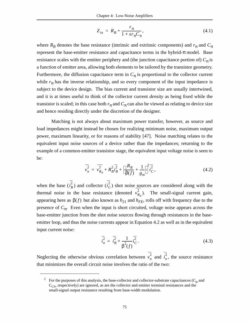
Chapter 4: Low-Noise Amplifiers
etry.
t
ce is
ined,
ze
and
utput
the
to the
een to
th the
gain,
s the
base-
valent
tance
, (4.1)
whereRB denotes the base resistance (intrinsic and extrinsic components) andrπ andCπrepresent the base-emitter resistance and capacitance terms in the hybrid-π model. Base
resistance scales with the emitter periphery and (the junction capacitance portion of)Cπ is
a function of emitter area, allowing both elements to be tailored by the transistor geom
Furthermore, the diffusion capacitance term inCπ is proportional to the collector curren
while rπ has the inverse relationship, and so every component of the input impedan
subject to the device design. The bias current and transistor size are usually intertw
and it is at times useful to think of the collector currentdensityas being fixed while the
transistor is scaled; in this case bothrπ andCπ can also be viewed as relating to device si
and hence residing directly under the discretion of the designer.
Matching is not always about maximum power transfer, however, as source
load impedances might instead be chosen for realizing minimum noise, maximum o
power, maximum linearity, or for reasons of stability [47]. Noise matching relates to
equivalent input noise sources of a device rather than the impedances; returning
example of a common-emitter transistor stage, the equivalent input voltage noise is s
be:
, (4.2)
when the base ( ) and collector ( ) shot noise sources are considered along wi
thermal noise in the base resistance (denoted ). The small-signal current
appearing here as but also known ash21 andhFE, rolls off with frequency due to the
presence ofCπ. Even when the input is short circuited, voltage noise appears acros
base-emitter junction from the shot noise sources flowing through resistances in the
emitter loop, and thus the noise currents appear in Equation 4.2 as well as in the equi
input current noise:
. (4.3)
Neglecting the otherwise obvious correlation between and , the source resis
that minimizes the overall circuit noise involves the ratio of the two:
2 For the purposes of this analysis, the base-collector and collector-substrate capacitances (Cµ andCCS, respectively) are ignored, as are the collector and emitter terminal resistances and thesmall-signal output resistance resulting from base-width modulation.
Zin RB
r π1 srπCπ+------------------------+=
vn2
vRB
2RB
2+ iB
2 RB
β f( )---------- 1
gm------+
2iC2
+=
iB2
iC2
vRB
2
β f( )
in2
iB2 1
β2f( )
------------- iC2
+=
vn2
in2
75
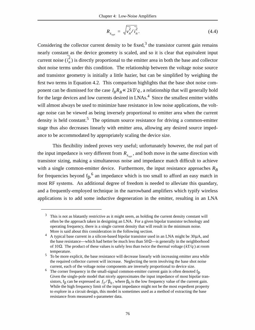
Chapter 4: Low-Noise Amplifiers
s
input
ector
ource
the
com-
hold
volt-
urrent
ter
mped-
t of
with
hieve
es
in
dary,
less
LNA
-
e
. (4.4)
Considering the collector current density to be fixed,3 the transistor current gain remain
nearly constant as the device geometry is scaled, and so it is clear that equivalent
current noise ( ) is directly proportional to the emitter area in both the base and coll
shot noise terms under this condition. The relationship between the voltage noise s
and transistor geometry is initially a little hazier, but can be simplified by weighing
first two terms in Equation 4.2. This comparison highlights that the base shot noise
ponent can be dismissed for the case , a relationship that will generally
for the large devices and low currents desired in LNAs.4 Since the smallest emitter widths
will almost always be used to minimize base resistance in low noise applications, the
age noise can be viewed as being inversely proportional to emitter area when the c
density is held constant.5 The optimum source resistance for driving a common-emit
stage thus also decreases linearly with emitter area, allowing any desired source i
ance to be accommodated by appropriately scaling the device size.
This flexibility indeed proves very useful; unfortunately however, the real par
the input impedance is very different from , and both move in the same direction
transistor sizing, making a simultaneous noise and impedance match difficult to ac
with a single common-emitter device. Furthermore, the input resistance approachRB
for frequencies beyond fβ,6 an impedance which is too small to afford an easy match
most RF systems. An additional degree of freedom is needed to alleviate this quan
and a frequently-employed technique in the narrowband amplifiers which typify wire
applications is to add some inductive degeneration in the emitter, resulting in an
3 This is not as blatantly restrictive as it might seem, as holding the current density constant willoften be the approach taken in designing an LNA. For a given bipolar transistor technology andoperating frequency, there is a single current density that will result in the minimum noise.More is said about this consideration in the following section.
4 A typical base current in a silicon-based bipolar transistor used in an LNA might be 30µA, andthe base resistance—which had better be much less than 50Ω—is generally in the neighborhoodof 10Ω. The product of these values is safely less than twice the thermal voltage ( ) at roomtemperature.
5 To be more explicit, the base resistance will decrease linearly with increasing emitter area whilethe required collector current will increase. Neglecting the term involving the base shot noisecurrent, each of the voltage noise components are inversely proportional to device size.
6 The corner frequency in the small-signal common-emitter current gain is often denoted fβ.Given the single-pole model that nicely approximates the input impedance of most bipolar transistors, fβ can be expressed as , whereβ0 is the low frequency value of the current gain.While the high frequency limit of the input impedance might not be the most expedient propertyto explore in a circuit design, this model is sometimes used as a method of extracting the basresistance from measured s-parameter data.
Rsoptvn
2in2⁄=
in2
IBRB 2kT q⁄«
kT q⁄
Rsopt
fT β0⁄
76
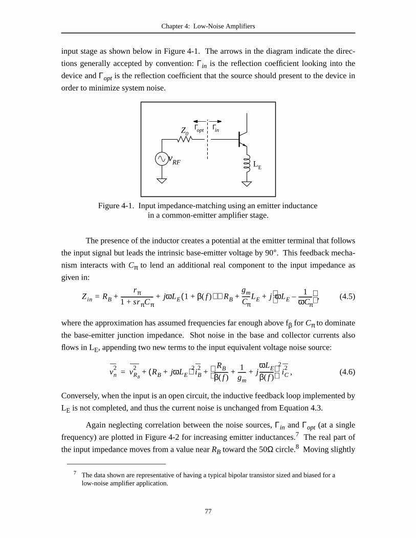
Chapter 4: Low-Noise Amplifiers
irec-
e in
llows
as
s also
d by
input stage as shown below in Figure 4-1. The arrows in the diagram indicate the d
tions generally accepted by convention:Γin is the reflection coefficient looking into the
device andΓopt is the reflection coefficient that the source should present to the devic
order to minimize system noise.
The presence of the inductor creates a potential at the emitter terminal that fo
the input signal but leads the intrinsic base-emitter voltage by 90°. This feedback mecha-
nism interacts withCπ to lend an additional real component to the input impedance
given in:
, (4.5)
where the approximation has assumed frequencies far enough above fβ for Cπ to dominate
the base-emitter junction impedance. Shot noise in the base and collector current
flows in LE, appending two new terms to the input equivalent voltage noise source:
, (4.6)
Conversely, when the input is an open circuit, the inductive feedback loop implemente
LE is not completed, and thus the current noise is unchanged from Equation 4.3.
Again neglecting correlation between the noise sources,Γin andΓopt (at a single
frequency) are plotted in Figure 4-2 for increasing emitter inductances.7 The real part of
the input impedance moves from a value nearRB toward the 50Ω circle.8 Moving slightly
7 The data shown are representative of having a typical bipolar transistor sized and biased for alow-noise amplifier application.
vRF
Z0
LE
Figure 4-1. Input impedance-matching using an emitter inductancein a common-emitter amplifier stage.
Γopt Γin
Zin RB
r π1 srπCπ+------------------------ jωLE 1 β f( )+( )+ += RB
gm
Cπ------LE j ωLE
1ωCπ----------–
+ +≅
vn2
vRB
2RB jωLE+( )2
+ iB2 RB
β f( )---------- 1
gm------ j
ωLE
β f( )----------+ +
2iC2
+=
77

Chapter 4: Low-Noise Amplifiers
is
r the
ginary
e (i.e.
to
con-
f the
e
cisely
lyy
in the direction of lower resistances isΓopt, although the absence of correlation in th
example has exaggerated the variation in ; to a first approximation, and hence fo
purposes of design, is essentially unchanged by the addition of LE. Another effect
rendered by assuming uncorrelated equivalent input noise sources is that the ima
part of the optimum source impedance equals that in the conjugated input impedanc
). This would be a desirable trait, asΓin andΓopt could then both be closed to
the center of the Smith chart (a 50Ω source impedance) by prefixing a base inductance
the stage depicted in Figure 4-1. In practice, however, correlation between and
tributes a component to the optimum source reactance ,9 where the
latter term is proportional to frequency and the base-collector capacitance [48]:
. (4.7)
The ratio under the radical in Equation 4.7 consists of the fully-correlated portions o
equivalent input noise sources (calculated withCµ considered in the device model). Th
correlation reactance prevents a simultaneous noise and power match from pre
8 More generally, the “50Ω circle” should be called the Z0 circle. Impedances plotted on a Smithchart can be normalized to any characteristic impedance; it need not be 50Ω.
9 At first, the concept of a correlation impedance might seem odd. Imagine, however, if the inputnoise consisted of a single frequency characterized by a fixed phase offset between the perfectcorrelated voltage and current components. This portion of the noise could then be cancelled ba judicious selection of the source impedance.
0.2 0.5 1 2
j0.2
−j0.2
0
j0.5
−j0.5
0
j1
−j1
0
j2
−j2
0
Γin
Γopt
Figure 4-2. Effect of emitter inductance on the input impedance of a common-emitter amplifier stage where the arrows indicate the direction of increasing LE;
correlation in the equivalent input noise sources has been neglected.
Rsopt
Rsopt
Xopt Xin–=
vn2
in2
Xopt Xin Xcorr+( )–=
Xcorr
ωCµgm
-----------v′n
2
i ′n2
------=
78

Chapter 4: Low-Noise Amplifiers
not
, but
icon-
igher
om-
nd
gies
ower
ues.
cir-
sues
vesti-
e fig-
ems.
nent,
uming
figure
ource
ge in
o-
et-
is
occurring, and effectively represents an error term in the design of LNAs. It is usually
a large error at frequencies reaching into the lower end of the microwave spectrum
should be remembered within the context of technology development. Advanced sil
based bipolar technologies often rely upon heavily-doped collectors to support the h
current densities needed for achieving faster (higher peak fT) transistors, a trend which
may begin to undermine continued improvement in LNA performance due to the conc
itant increase in Cµ. There are, of course, many other intricacies involved with LNAs, a
the following sections take a deeper look at a handful of narrowband amplifier topolo
and some of the shadows they cast in the semiconductor technology space.
4.2 Technology Considerations for LNAs
In a quest to realize gain and controlled impedances in a low noise and low p
framework, the design of an LNA brings together a number of poignant technology iss
Investigating a range of circuit topologies and possibilities of developing techniques to
cumvent limitations are important steps in determining the extent to which these is
represent fundamental barriers in performance. But before embarking on such an in
gation, a means of considering comparative circuit performance is needed, and nois
ure provides a convenient first-order description for LNAs in RF and microwave syst
Indicating the extent to which the signal to noise ratio (SNR) is degraded by a compo
noise figure proves to be a salient measure of wireless receiver sensitivity.10
Given an equivalent input noise source representation of an element, and ass
that the current ( ) and voltage ( ) noise components are uncorrelated, the noise
(expressed in dB) for that element can be calculated by:
, (4.8)
whereZs is the source impedance and is the thermal noise associated with the s
resistance. Referring to the noise expressions derived for the common-emitter sta
10 There are two caveats that should be remembered in using noise figure. First, noise figure prvides no indication of gain; a wire may have a 0dB noise figure, but its decided lack of gain failsto protect the SNR from noise in subsequent stages. In this sense, noise measure could be a bter metric from a system perspective. A second criticism leveled at noise figure is that it is afunction of the source resistance, a property which can lead to confusion when the resistancenot fixed. In absolute terms, an amplifier having a 3dB noise figure and meant for a 75Ω systemcontributes more noise than an amplifier with a similar 3dB noise figure but intended for 50Ωapplications. The ratio of the noise in the two cases is 75Ω/50Ω.
in2
vn2
NF 10vRs
2vn
2Zs
2in2
+ +
vRs
2-----------------------------------
log 10 1vn
2Zs
2in2
+
vRs
2----------------------+
log= =
vRs
2
79
Chapter 4: Low-Noise Amplifiers
noise
r-
h
oper-
gain
oise
ult in
ve
ain
by
device
osen
th
rn
f
Section 4.1, noise figure is seen to depend upon the magnitude of the transistor
sources—and thus uponRB, IC, and IB—with a corner frequency in the behavior dete
mined by the fT of the device through .11 With the prevalence of shot noise in bot
and , it comes as no surprise that bipolar transistors generate less noise when
ated at lower current levels. The mitigating factors in this trend are that the current
begins to fall and the intrinsic portion of the base resistance increases asIC is reduced.
Finding the optimum bias current (density) is thus a vital first step in designing low-n
amplification stages.
Denoting the argument to the logarithm function in Equation 4.8 asF, varying the
source impedance to find its minimum value, and expressing the approximate res
terms of explicit transistor parameters gives [49]:
. (4.9)
This result has been simplified by restricting the range of frequencies to be abofβ( ), further assuming that the low frequency small-signal current g
( ) equals the DC (large-signal) current gain ( ), and
neglecting the base resistance in comparison torπ.12 Writing the collector current as a
product of the current density ( ) and the emitter area (AE), and then normalizing the
base and emitter resistances to this area yields:
, (4.10)
with and representing the base and emitter resistances associated with a
having an emitter geometry of the minimum width and 1µm2 in area. A subtle change
indeed, but this form demonstrates that the minimum noise figure achievable in a ch
11 Though not explicitly shown earlier, the effect of the emitter resistance in the equivalent inputnoise sources is additive with the base resistance, and can be incorporated by replacing wi
in Equations 4.2 and 4.6. While the situation may change in highly-scaled devices, theemitter resistance has routinely been made quite small (relative to the base resistance) in modepolysilicon emitter technologies, to the point whereRE does not make a strong contribution tothe noise.
12 The statement is very similar to an assumption made previously in the noise analysis oSection 4.1, namely that . One further approximation made in Equation 4.9 isthat the collector current ideality factor is dropped from the expression for the transconductance(i.e.nF is assumed to be unity). This is a very good approximation for nearly all silicon-basedbipolar transistors in use today.
β f( )
RBRB RE+
vn2
in2
Fmin 1 1β0----- 1
β0----- 2
qICkT-------- RB RE+( ) 1
β0----- f
2
f T2
------+
++ +≅
ω r πCπ[ ] 1–»β0 IC∂ IB∂⁄= βDC IC IB⁄=
rπ RB»kT q⁄( ) I BR
B»
JC
Fmin 1 1β0----- 1
β0----- 2
qJC
kT-------- R′B R′E+( ) 1
β0----- f
2
f T2
------+
++ +≅
R′B R′E
80

Chapter 4: Low-Noise Amplifiers
e fig-
an-
base
ase-
tances
,
it is
e
n the
al to
ol-
will
d,
;
n in
ide a
ri-
low
r. As
technology is a function of the current density (β0, , andfT all depend on ) and not
the transistor size; the optimum source impedance associated with the minimum nois
ure decreases as the device grows, but remains essentially unchanged.13
By way of completing the story, the unity current-gain frequency for a bipolar tr
sistor can be related to the current density—for bias currents well below the onset of
pushout—as:
, (4.11)
where τF denotes the forward base transit time and the base-emitter and b
collector junction capacitances are defined per unit area analogously to the resis
in Equation 4.10. The current density at which the optimum (lowest)Fmin occurs can then
be determined by inserting this expression forfT, approximatingβ0 and as constants
and solving ; this algebraic handiwork provides [49]:
. (4.12)
While subject to the same limitations as the noise figure expression from which
derived (restricted, most notably, to frequencies abovefβ), Equation 4.12 does convey th
often-overlooked significance of the role played by transistor junction capacitances i
performance of RF/microwave LNAs. That the optimum current density is proportion
indicates thatthe attainable noise figure which can be extracted from a techn
ogy, and the power consumption required to realize this minimum noise condition,
both decrease as the junction capacitance is reduced. When the source resistance is fixe
LNA power dissipation and noise figure will approximately follow the square root of
the power saved by lowering the optimum bias current density through a reductio
capacitance is partially offset by the necessity of using a larger transistor to prov
noise match to the source.
Surprisingly mute in all of this behavior is the ubiquitous current gain . P
marily bound by junction capacitances in the LNA regime of RF frequencies and
noise bias currents, goes largely unaffected as and scale togethe
13 This is more true for the purposes of an LNA, for which noise constraints mandate the minimumemitter width, than it is in general. Until current crowding starts to become an issue, increasingthe emitter width for a given emitter area and bias current yields a higher transistor fT due toreductions in bothCµ andτF. The changes inτF result from a second-order effect involving cur-rent spreading in the collector [50].
R′B JC
Fmin
fT1
2π τF kT q⁄( ) C′jE C′µ+( ) JC⁄+[ ]------------------------------------------------------------------------------=
C′jEC′µ
R′BFmin∂ JC∂⁄ 0=
JCopt2π C′jE C′µ+( )kT
q------
β0 f2
1 4+ π2β0τF2
f2
-------------------------------------≅
C′jE C′µ+
JCopt
β f( )
β f( ) JCoptC′jE C′µ+
81

Chapter 4: Low-Noise Amplifiers
nt of
g an
o close
tance
cog-
ude
into
trates
se in
re,
hnol-
s
been
n
put
that
mitter
ini-
the
els.
50
ally
ce
er
might be expected, the thermal noise contributors in the transistor are independe
capacitance while the shot noise sources follow in tune with the bias current, yieldin
increase in the optimum source resistance as decreases. For frequencies not to
to fT, the largest term in the voltage noise expression (Equation 4.2) is the base resis
thermal noise; ignoring the somewhat smaller and terms for the moment, and re
nizing that a current density of corresponds to having , a rather cr
approximation for the optimum source resistance can be proposed:
. (4.13)
An appendix could be filled with the litany of assumptions that have gone
Equation 4.13, but this relationship does capture the prevailing behavior and demons
that a reduction in the optimal collector current density ( ) necessitates an increa
transistor emitter area (AE) by to maintain a desired source resistance. As befo
the emitter stripes are assumed to be drawn at the minimum width allowed by the tec
ogy, is the base resistance for a 1µm2 device,14 and the low frequency current gain i
taken to be equal to the DC current gain. Furthermore, the operating frequency has
constrained to a band of frequencies far enough above fβ for Cπ to dominate the base-
emitter impedance, but yet enough below fT so that is still appreciably greater tha
unity. And finally, it should not be forgotten that correlation between the equivalent in
noise sources has been, well, forgotten in the derivation of .
Couched within this discussion of technology considerations is a framework
has been established for designing low-noise amplifier stages based upon common-e
topologies. The approach begins by identifying the collector current density that m
mizes noise at the frequency of interest (via Equation 4.12).15 It is important to note that
this current density, denoted , is a technology parameter and is subject only to
design frequency; there are no “knobs” to be turned at the circuit or system design lev
Next on the agenda is to size the device to placeΓopt on the 50Ω circle by scaling the
emitter area (Equation 4.13 or, more accurately, using Equation 4.4). The choice of aΩcharacteristic impedance is more tradition than physical law; while an LNA is typic
14 Also as before, the emitter resistance can be incorporated by summing it with the base resistan(i.e. ).
15 Being tacitly practiced here is a fairly typical microwave design ploy: in adjusting the bias cur-rent and looking atFmin, the source impedance is allowed to go wherever it needs in order tominimize the noise at each bias condition. Having the impedances “track” the swept parametproves exceedingly useful, and is the reason why so many definitions of gain are used in thedesign and analysis of microwave circuits.
JCopt
iB2
iC2
JCoptβ f( ) β0=
Rsopt
1AE------- β0R′B
kT q⁄JCopt
------------≅
JCopt
JCopt
R′B
R′B R′B R′E+→
β f( )
Rsopt
JCopt
82

Chapter 4: Low-Noise Amplifiers
filter,
ided
emitter
g
tely
in
ing
evice
t.
s, a
f the
hee
is
t
constrained by interfacing with an input from an antenna and perhaps a low-loss
moving toward higher impedances might result in lower power consumption, prov
that the corresponding loss in gain does not become too severe.16 With the optimum
source resistance having been chosen, the design is completed by setting first the
inductance and then the base inductance to provide an input impedance of 50Ω as
reflected in Equation 4.5. Tuning LE allows a 50Ω resistance to be established lookin
into the base, and LB is used to resonate the residual input capacitance. By appropria
sizing the transistors and inductors, this approach—summarized pictorially
Figure 4-3—yields the optimum noise figure afforded by a technology while transform
the input impedance to provide a power match. Considering that only one active d
has been used, it should not be surprising that this topology will prove difficult to bea
4.3 Alternative LNA Topologies
Noting that design simplicity often carries the day in RF and microwave circuit
good place to begin a search into alternative LNA topologies is with an examination o
16 Regardless of the frequencies involved and whether voltage or power is being considered as tsignal, transistors fundamentally remain transconductance devices and thus need to drive largimpedances to realize gain. If all of the circuit impedances could be scaled inversely with thetransistor size, then the available gain (to first order) would remain the same as the bias currentreduced. Unfortunately, in an integrated circuit, the maximum load impedance is limited by theinductor loss, and thus the decrease in transconductance resulting from the lower bias currenassociated with a higher source resistance will reduce the gain.
0.2 0.5 1 2
j0.2
−j0.2
0
j0.5
−j0.5
0
j1
−j1
0
j2
−j2
0
Figure 4-3. Illustration of achieving a simultaneous noise and power match in acommon-emitter transistor stage; correlation in the equivalent input noise
sources has been neglected.
Γin
Γopt
Increasing LE
Increasing LE
Increasing LB
Increasing LB
Increasing AE (at constant JC)
Increasing AE (at constant JC)
AE: emitter area
LB: base inductance
LE: emitter inductance
JC: collector current density
83

Chapter 4: Low-Noise Amplifiers
pre-
lation
1], and
, and
ond-
lector
ppli-
is
l in
tance
for-
ition
-base
hunted
se
ever,
ance.
h is
ed-
is
induc-
taking
remaining single-transistor amplifier connections. With all of the emphasis in the
ceding sections upon analyzing a common-emitter stage, it should be no small conso
that the same equivalent input noise sources represent a common-base transistor [5
so all of the expressions derived for the optimum current density, source impedance
noise figure apply equally well to the common-base configuration [52]. Some sec
order differences in gain and noise figure exist due to subtleties in the base-col
capacitance feedback mechanism [53], but are generally not too significant for LNA a
cations operating at frequencies below fT.17 One difference that is significant, however,
the input impedance; for a common-base transistor:
, (4.14)
with the emitter resistance (RE) now being explicitly included. This impedance isZin for
the common-emitter stage divided by the factor , and will typically be smal
magnitude and predominantly resistive. Except for low bias currents, the input resis
will be too small to yield a good power match to most RF sources—a problem that un
tunately seems to keep recurring.
A convenient solution for the common-emitter design was afforded by the add
of some series-feedback inductance, a technique for which the analogue in common
stages is to attach a capacitive impedance at the base terminal. When the base is s
(to an RF ground) through a capacitanceCB, the input resistance of the common-ba
device increases by . For this capacitor to have its intended effect, how
the base bias will need to be applied through some sort of reasonably large RF imped
Coupling the bias through an inductor or a resistor would certainly qualify; the catc
that for the transistor to function properly (i.e. to provide gain and low noise), the imp
ance presented byCB must be small over the range of frequencies for which the LNA
being designed. Nothing is new here either, as much the same can be said for the
tance in the common-emitter stage. Grounding the emitter through a largeLE degenerates
the gain and increases the equivalent input voltage noise (Equation 4.6), the latter
17 The feedback admittancey12—which reduces the transistor gain, increases the noise figure, cre-ates stability issues, and may possibly contribute to global warming—can be expressed as
for a common-emitter device, and is a factor of largerwhen the same transistor is used in the common-base configuration (this holds up to about fT,and neglects the transistor output resistance that contributes a 1/ro term). This does not tell thewhole story, however, as will be on order of unity for typical silicon bipolar LNAs. Asfrequencies approach fT, the available gain from emitter to collector falls more rapidly than thatfrom base to collector so, for similary12 values, the common-base connection exhibits lowergains and higher noise figures than the common-emitter variant [53].
y12 sCµ– 1 s Cµ Cπ+( )RB+[ ]⁄= gmRB
gmRB
Zin RE1
gm------ β f( )
1 β f( )+--------------------
RB
1 β f( )+--------------------+ +=
1 β f( )+
Cπ gmCB( )⁄
84

Chapter 4: Low-Noise Amplifiers
ich
-
mitter
as
s
nce
lts in
ulta-
not
very
nt
lied
radial
pt for
istor
mon-
So
ped-
gain
axi-
well
) is
a
riving
).
to
ater
-y
along with it. The distinction between these two configurations, and one wh
proves to be of consequence, is that fT works with the input resistance in the common
emitter case and against it when using a common-base transistor. Approximating
as , the resistance added by an emitter inductance to the input of a common-e
device is , allowing the impedance of this inductor to be expressed
. The extra input resistance induced byCB in a common-base stage ha
the reciprocal relationship: , with the capacitor imposing an impeda
between the base and (an RF) ground. The weaker ground that resu
the common-base stage—the impedance is higher by a factor of —makes sim
neously obtaining gain with both noise and power input matches a very difficult (if
impossible) task indeed. This story may change for designs targeting frequencies
near, or beyond, the transistor fT. Furthermore, higher frequencies may allow a convenie
transmission line implementation of the base circuitry; the DC bias could be app
through a high characteristic impedance trace, and an open-ended stub (or
stub) could be used to provide a narrow-band capacitance at the base. But exce
broadband LNA applications or those that push the very limits of the available trans
technology, a common-base input stage yields no fundamental advantage over a com
emitter topology, and mostly just results in a more contentious design.
The last of the three single-transistor configurations is the emitter-follower.
commonly seen as a buffering stage due to its high input impedance, low output im
ance, and nearly unity voltage gain, that a common-collector device can yield power
through its impedance transformation properties might easily be overlooked. The m
mum available (power) gain attainable from a transistor used in this fashion is fairly
approximated as ,18 whereAv is the voltage gain,Zin is the
same as that looking into a common-emitter stage when (in Equation 4.5
replaced by the load impedance, andZout corresponds to the input impedance of
common-base stage (as given in Equation 4.14) when the resistance of the source d
the emitter-follower is included with the transistor base resistance (i.e.
Although follows for lower frequencies—extending approximately
the point where —this ratio of impedances can be shown to be gre
than unity for , indicating that power gain is in fact available beyond fT.19 The
18 The maximum available gain of a transistor is the power gain that can be obtained when simultaneous conjugate impedance matches are presented at both the input and the output. It is onldefined over the range of frequencies for which a transistor is unconditionally stable, which is tosay that the device will not oscillate for any passive termination that could be affixed to eitherthe output or the input. Emitter-followers specifically tend not to cooperate with capacitiveloads, a topic that Section 4.4 will cover in some detail.
Rsopt
gm Cπ⁄ωT
Rin ωTLE≅ZLE
ωRin ωT⁄≅Rin 1 ωTCB( )⁄≅
ZCBωTRin ω⁄≅
ωT2 ω2⁄
λ 4⁄
Gma 10 Av2
Zin Zout⁄( )log≅jωLE
RB RB Rs+→Zin Zout⁄ β f( )
β f( ) gm RB Rs+( )=
β f( ) 1=
85

Chapter 4: Low-Noise Amplifiers
some
ow
quiva-
mon-
base
lving
volt-
t will
own
ure,
this
nals.
wer
ed as
by
a
han
ut
lower
uired
diffi-
influ-
e
gain at such frequencies will not be large, yet this observation should at least lend
sense of the potential for realizing a common-collector RF amplifier.
Given the apparent feasibility of amplification, the next question pertains to h
the noise performance of an emitter-follower compares, and the answer is that the e
lent input noise sources for this connection are also very similar to those for a com
emitter stage. Taking the output from the emitter instead of the collector includes the
current in the numerator of the current gain expression, and so all of the terms invo
shot noise are multiplied by the factor , resulting in:
, (4.15)
for the voltage noise source and a current noise represented by:
. (4.16)
The appearance of the dynamic emitter resistance ( ) in the component of the
age noise stems from the emitter not being at ground. However—as this componen
generally remain only a minor contributor to the voltage noise—the expressions sh
above will be essentially equivalent to those for a common-emitter transistor until
approaches unity, allowing the previously-derived relationships for optimum noise fig
current density, and source resistance to be applied with reasonable accuracy.
There is one significant drawback to the common-collector configuration, and
is in having only a base-emitter junction sitting between the output and input termi
Despite its reputation as a buffer amplifier, the isolation afforded by an emitter-follo
decreases in conjunction with the current gain, and so very little decoupling is provid
frequencies begin to push toward fT. Possessing a reverse transconductance given
for any usable frequency, this conductance will be roughly
factor of higher throughout the RF spectrum for a common-collector device t
that exhibited by the other two incarnations.20 The increased interaction between inp
and output loading that results at higher frequencies hinders the performance of a fol
as a voltage buffer and limits its usefulness as an RF amplifier when isolation is req
between an antenna and internal circuitry. Furthermore, poor isolation makes for a
cult design as the matching networks and impedances on one side of the amplifier
19 At first this may seem to run afoul of fundamental physics, being that the power gain cannot bgreater than one when both the voltage and currents gains are less than unity. However,refers to thecommon-emitter current gain; the current gain from base to emitter is .
β f( )1 β f( )+
β f( ) 1 β f( )+( )⁄[ ]2
vn2
vRB
2RB
1gm------+
2 β f( )1 β f( )+--------------------
2+ iB
2 RB
β f( )---------- 1
gm------+
2 β f( )1 β f( )+--------------------
2iC2
+=
in2 β f( )
1 β f( )+--------------------
2iB2 1
1 β f( )+--------------------
2iC2
+=
1 gm⁄ iB2
β f( )
y12 1– RB β f( ) gm⁄+[ ]⁄≅Cπ Cµ⁄
86

Chapter 4: Low-Noise Amplifiers
he
ffers
con-
sult,
mall
in a
mon-
per-
mong
paci-
mitter
en-
ance
n
nve-
chal-
hile
mption
rrent
e tran-
o a
ss
ence those on the other side.21 Compounding the gravity of this consequence is that t
collector of a forward-active bipolar transistor, when used as a common terminal, o
little opportunity to affect the transistor impedances through local feedback—a trait
veniently exploited in both the common-base and common-emitter forms. As a re
when the goal is to achieve a fully-integrated solution, it appears quite likely that the s
improvement in intrinsic noise figure offered by an emitter-follower will be swamped
sea of matching network issues.
It is seen from the preceding discussion that the common-base and com
collector connections are very similar to the common-emitter device in terms of noise
formance throughout most of the RF frequency range. Small differences do exist a
the transistor configurations in how they are inhibited by parasitic resistances and ca
tances; bipolar transistors feature a little more (power) gain when used as common-e
devices, exhibit slightly lower noise in the emitter-follower form, and yield some pot
tially useful impedance properties along with intermediate gain and noise perform
when the base is taken as the common terminal.22 That the common-emitter connectio
has become the predominant choice for LNA input stages is owed largely to the co
nience that it affords; the alternative uses of a single transistor entail a greater design
lenge and fail to offer improvements of any real consequence to RF performance. W
stages can be cascaded to increase gain or bandwidth at the cost of power consu
and noise figure, a couple of multiple transistor incarnations—the cascode and the fT dou-
bler—may also be worth investigating as alternatives for LNA applications.
4.3.1 Unity Current Gain Frequency (fT) Doubler
A recurrent theme in this section has been to examine the effects of falling cu
gain on noise, gain, and impedances as the frequencies being handled approach th
20 A more commonly-encountered measure of isolation for RF purposes is phrased in scatteringparameters—a set of small-signal parameters that characterize a network in terms of unitlessgains. Expressed in dB,s12 conveys the rejection an amplifier provides (measured at its input)of a signal driven onto its output port. For a common-emitter or common-collector transistor, toa first-order degree of accuracy, and assuming that the source and load resistances are equal tcharacteristic impedance Z0, , where the base-emitterimpedance is denoted . This isolation term can be considered as the reversetransconductance multiplied by the resistance in the RF source and a factor that accounts for loin the base-emitter circuit.
21 A device offering perfect isolation is also known as being unilateral, a description rooted in thenotion that signals can only propagate through the device in the forward direction (i.e. thereverse gain ).
22 The higher power gain of the common-emitter device refers to the maximum stable gain (ormaximum available gain, if the transistor is unconditionally stable) at low frequencies. Forhigher (RF) frequencies, the common-base transistor can provide slightly higher gains.
s12 2– y12Z0 RB Zπ+( ) Z0 RB Zπ+ +( )⁄≅Zπ β f( ) gm⁄=
s12 0=
87

Chapter 4: Low-Noise Amplifiers
one
of
d in
tself,
base-
single
s can
urrent
input
cur-
cur-
both
olt-
ring
nsis-
gain
sistor fT. Observing the deleterious effects of low current gain at RF frequencies,
might begin to ponder whether fT is fundamental, or rather if there is some means
increasing the unity current gain frequency beyond the device fT. As an affirmative
answer, enter a class of circuits loosely known as fT doublers. By way of first-order
thinking, if the input signal is impressed across two base-emitter junctions place
series, the effective input capacitance—and thus the input current—is halved. By i
this series connection accomplishes little; the input voltage splits across the two
emitter junctions and thus each transistor produces half the output current that a
device would have generated. However, if the collectors of the two series transistor
be connected such that the output currents add in phase, then the overall output c
would be the same as that sourced through a single transistor. With the associated
current having been lowered by a factor of two, the current gain—and hence the unity
rent gain frequency—is effectively doubled.
One particularly elegant single-ended embodiment of the fT doubler concept was
implemented by Battjes in the late 1970s and is depicted in Figure 4-4 [54][55]. The
rent mirror in the emitter of the input transistor ensures that the same current flows in
devices driving the output, effectively applying the transconductance to the full input v
age. Meanwhile, the loading of the mirror increases the input impedance, lowe
the input current associated with a given output signal level. Assuming matched tra
tors each having current gain characteristics described by , the overall current
(h21) realized by this circuit can be expressed as:
. (4.17)
vRF
Figure 4-4. Battjes’ fT doubler circuit.
2Cπ
β f( )
h21 2β f( )1 β f( )+2 β f( )+--------------------=
88
Chapter 4: Low-Noise Amplifiers
ated
cies
s the
nd
se
the
t and
and
ele-
evices.
and
tion
ncy
e that
tors in
of a
itter
ever,
plifi-
ol-
g
n-
The current gain of the Battjes doubler thus follows up to a pole frequency loc
where and a subsequent zero at . A doubling is effected for frequen
below , beyond which the pole-zero doublet indicated in Equation 4.17 cause
current gain to asymptotically approach .
While this increase in fT is real, and this technique has proven useful for wideba
amplifiers [56][57],23 it is important to realize that there is no corresponding increa
observed in the power gain (i.e. this is an fT doubler, not an fMAX doubler). Concomitant
with the doubling of the current gain is a halving of the output impedance driven by
transconductance, leaving the available (power) gain unchanged. Similarly, the sho
thermal noise contributions from each transistor are also unaffected by splitting
recombining the signal path, resulting in equivalent input noise levels that are actually
vated above the single-transistor common-emitter stage due to the cascaded d
Hence, while their simplicity of connection and biasing allows fT doubler stages to easily
replace common-emitter transistors in a variety of applications, the higher noise
equivalent power gain of the doubler fail to make a compelling argument in the realiza
of low-noise amplifiers.
4.3.2 Cascode
Another connection that is often invoked in the quest for improved freque
response is the cascode: a DC-coupled common-emitter, common-base cascad
reuses the same bias current for each stage. Shown with impedance matching induc
Figure 4-5, the conventional thinking behind the cascode is that the input loading
Miller-multiplied Cµ is suppressed by keeping the voltage gain across the common-em
device near unity and instead obtaining the gain via a common-base transistor. How
as capacitive loading tends not to be an issue for reactively-matched narrowband am
ers, this suppression property is not significant in most wireless applications.24
23 One modification of the fT doubler circuit shown in Figure 4-4 is to balance the collector-emittervoltages by adding a diode-tied device in the collector of the mirror output transistor. This canbe important when using III-V HBTs not only for self-heating considerations, but also becausethe transistor fT generally falls as VCE is increased beyond a certain level. GaAs, InGaAs, andInP feature a pronounced velocity overshoot effect; the electrons initially fill a low effectivemass conduction band and then reach a much heavier band at higher energies, causing the clector transit time to reach a minimum at low VCE values [58]. Secondly, III-V transistors fabri-cated via MBE often have thin (and lightly-doped) collectors that are fully depleted for VCE~0.In this case Cµ is no longer reduced by increases in VCE.
24 This property of a cascode can be more of a hindrance than a help, as the impedance-reducinquality of shunt feedback can be usefully employed to aid the realization of an input match. Onepublished cascode amplifier has featured an impedance inserted in series between the two trasistors, implemented for the explicit purpose of re-instantiating the Miller effect [59].
2β f( )
β f( ) 2= β f( ) 1=
fT 2⁄β f( )
89

Chapter 4: Low-Noise Amplifiers
ted by
the
pen-
nce
e R
,
nite)
ing
gains
i-
Of greater consequence is the manner in which the feedback path represen
Cµ limits gain and stability in a common-emitter stage. As an illustration, consider
inverting amplifier configuration shown in Figure 4-6. The op-amp represents the o
loop gain afforded by the transistor ( ), and the base-collector capacita
connects around this gain element to a node defined by the intrinsic (RBi) and extrinsic
(RBx) portions of the base resistance. Driven through a source having an impedancs,
the magnitude of the voltage gain is limited to , where
independent of the intrinsic transistor gain and assuming perfectly-resonated (infi
input and output impedances.25 The cascode amplifier can provide a win by sidestepp
this feedback issue and the associated stability problem of having appreciable loop
25 Particularly at low frequencies, the realizable transistor gain will generally be restricted to bewell below this value, as the inductive source impedance required to resonate the input capactance can lead to stability problems. See Section 4.4 for a more detailed analysis.
vRF
Z0
LE
LB
VDC
Figure 4-5. Cascode amplifier stage with input impedance matching.
Av gmZout–=
fµ f⁄ fµ 2πCµ Rs RBx+( )[ ] 1–=
RBx
Cµ
vout
−
+RBiRs Av
vin
Figure 4-6. Intrinsic feedback within a common-emitter stage.
90

Chapter 4: Low-Noise Amplifiers
-base
tes the
des
in
reased
imum
able
n be
cas-
stage
tacked
her
-stage
ech-
of
lifier
rs as
with
that
e tran-
tu-
ed
rt
at high frequencies. But tempering any newfound enthusiasm is that the common
transistor is also limited by a feedback mechanism as the base resistance degenera
gain. An additional limitation with the cascode connection is that it largely only tra
one stability problem for another; both sides of this trade-off will be examined
Section 4.4.
Regardless of the competing set of issues that the cascode introduces, its inc
output impedance does yield a palpable improvement in power gain, where the max
available gain from the cascode is on the order of higher than is achiev
from a common-emitter device at the same bias current.26 Also improved through cas-
coding is the isolation; the attenuation from output to input is much higher than ca
achieved from other single-stage designs. In fact, the low internal impedance of the
code helps to isolate the input from the output to a greater extent than some two
designs manage to achieve. But these benefits do not come without a price; the s
devices eat into supply headroom,27 and the interstage noise mismatch leads to a hig
noise figure than could be achieved with a cascade of common-emitter stages.28 The sec-
ond of these costs summarizes a general lesson to be taken from studying the fT doubler
and cascode topologies: adding more devices in the signal path, even in these single
designs, can only hurt the amplifier noise figure. Unfortunately, there are no circuit t
niques which can be found to overcome this fundamental technological hurdle.
4.3.3 Effects of Inductor Loss
As exemplified in this chapter, inductors play a prevalent role in the design
LNAs for RF/microwave receivers. The gain and noise characteristics of an amp
stage can be dramatically improved over a finite bandwidth by incorporating inducto
impedance matching elements. Along with inductance, however, inductors bring
them a number of loss mechanisms that can significantly impact the amplifier. Noting
the series resistance terms associated with the base and emitter inductors add to th
26 Sadly, much of this gain is thrown away in the inductor loss, but the improvement can be moreappreciable with MOSFETs and III-V transistors due to their lower output resistances (ro).
27 When the supply voltage has been fixed due to other constraints, the stacked devices might acally be a benefit. Splitting the supply voltage across two transistors can mitigate VCE break-down and self-heating concerns, and could potentially lead to a higher fT (see Footnote 23).
28 The higher noise figure of the cascode is sometimes explained as resulting from the suppressgain of the input transistor. Even in the cascode structure, however, the noise contributions ofthe common-base device are still reduced by the available gain of the common-emitter transistowhich precedes it. A more correct way of looking at the higher noise figure is to recognize thathe output impedance of the common-emitter device is generally not particularly close toΓoptfor the cascode transistor, and it is this mismatch that increases the noise.
10 gmro( )log
91

Chapter 4: Low-Noise Amplifiers
A
on-
ok
de an
nce
DC
um
-
ut
to a
sis-
n the
bout
itic
plifier
ped-
aving
quiva-
s in L
eping
input
e reac-
o
apaci-
ence
ctory
n
sistor terminal resistances RB and RE, it can be seen (through Equation 4.9) that the LN
noise figure might sustain an appreciable hit from inductor loss—particularly when
chip spirals are being used.29 To help convey a sense of the magnitude, it is useful to lo
at a representative example. A typical silicon-based bipolar transistor, sized to provi
optimum noise match to a 50Ω source when biased at , might have a base resista
of 8Ω and a 1Ω resistance in the emitter terminal. Assuming a current gain of 80 at
and an ratio of 4 at the operating frequency (associated with ), the minim
achievable transistor noise figure (NFmin) is determined to be 1.50dB. Borrowing induc
tor sizes of 0.7nH and 0.4nH for LB and LE from the 5.8GHz design example carried o
in Chapter 5, taking as a representative value and attributing all of the loss
series resistance, an additional 8Ω needs to be considered with the base and emitter re
tances in Equation 4.9 to account for the inductors. From this calculation, the loss i
matching inductors is seen to bump the minimum realizable LNA noise figure up by a
0.4dB (to 1.91dB)—a rather significant effect indeed!
Continuing with the model of combining inductor loss with the terminal paras
elements, it becomes evident that the source resistance needed to minimize the am
noise is also affected. The inductors contribute both thermal noise and additional im
ances to the equivalent input noise voltage (as expressed in Equation 4.6) while le
the corresponding noise current (Equation 4.3) unchanged. As the ratio of these e
lent sources relates to the optimum source resistance, increases due to the losB
and LE. To compensate, the emitter area of the input transistor can be increased—ke
the same current density—to reestablish an optimum noise condition to match the
source. Finally, though not surprisingly, the reactive portion ofΓopt also fails to emerge
unscathed; the parasitic capacitances associated with the inductors supplement th
tances of Cπ and Cµ. The matching inductance (mostly in LB) thus needs to be reduced t
returnΓopt to the line along the center of the Smith chart.30 An iterative design
loop results, where inductor loss necessitates a larger input transistor, but the extra c
tance associated with the larger transistor and the inductor allow a smaller—and h
lower loss—inductor to be used. Fortunately, this loop generally reaches a satisfa
conclusion after just two or three iterations.31
29 These inductor series resistance terms impact every measure where RB and RE appear,encroaching upon many aspects of amplifier performance (stability and isolation included).
30 Or, to phrase this in a manner less reliant upon Smith charts, the reduction in the matchinginductance is needed to return the amplifier input resonance to the desired center frequency ithe face of the additional parasitic capacitances brought on by the inductors.
31 As is often true of high frequency amplifier design: no pain, no gain.
JCopt
fT f⁄ JCopt
Q 5=
Rsopt
X 0=
92
Chapter 4: Low-Noise Amplifiers
ple-
ived
, espe-
r the
e gain
tral-
nduc-
pli-
paci-
prove
duc-
e, as
as a
l util-
exer-
crip-
ring
nta-
effi-
rent
strate
for a
bility
om-
a two-
e
The preceding example brings to light another lesson regarding integrated im
mentations of matching and tuning networks: what might seem like a win when conce
with lossless components may well be washed out in the loss of real passive devices
cially when the attendant area penalty is considered. As one example, conside
previously-discussed base-collector capacitance and its deleterious effects upon th
and isolation of a common-emitter transistor. In principle, it should be possible to neu
ize this capacitance over a narrow band of frequencies by resonating it with a shunt i
tor.32 However, the loss associated with an integrated inductor is likely to actuallylower
the base-collector impedance below that of the intrinsic junction, in turn hurting the am
fier performance more than it helps. Similarly, using an inductor to resonate the ca
tance sitting on the inner node of a cascode would seem to be an opportunity to im
upon the stability, gain, and noise figure characteristics of an LNA. But here again, in
tor loss will generally erase any benefits in both gain and noise figure. Furthermor
will be shown in the following section, stability in the cascode can be better handled
consideration in sizing the common-base transistor. This is not to dismiss the genera
ity of inductors in many settings, but merely to indicate that some caution should be
cised in evaluating each new application.
4.4 Transistor and Amplifier Stability
To the conventional analog IC designer, analyses of stability are rooted in des
tions of loop gain and phase carrying names like Routh, Nyquist, and Bode. Ventu
into a culture of microwave circuit design that has grown up around two-port represe
tions, stability parameters derived from impedances or (equivalently) reflection co
cients, and Smith chart-based stability circles tends to leave one’s mouth agape.33 An
improved scenario would be to establish a comfort level in believing that these diffe
considerations of stability are at least consistent. Rather than attempting to demon
mathematical equivalency, the goal here is to interpret some typical stability circles
transistor stage and then to try to understand why these conditions of potential insta
might exist.
Traditional microwave definitions of stability parameters and circles can be c
pletely established from a set of small-signal (e.g., s-parameter) measurements on
32 A DC-blocking capacitor will be needed in series with the neutralizing inductor unless the pre-ferred bias condition is .
33 The reverse situation is also true: most microwave designers are no more comfortable with phasmargins than IC designers are with stability circles.
VBC 0≅
93

Chapter 4: Low-Noise Amplifiers
dix,
ircles
Source
d in
sive)
which
nal
that
ignal.
sus-
ld be
g to
e of
point.
d-
port element. Stability circles, for which definitions have been supplied in the Appen
delineate a region of impedances that can lead to instability. Not surprisingly, these c
are drawn on a Smith chart, and are defined for both source and load impedances.
stability circles for a common-emitter transistor at two frequencies have been plotte
Figure 4-7.34 In this case, the Smith chart represents the set of all possible (pas
source impedances, and the circles indicate the collection of those impedances for
. Having a reflection coefficient greater than unity indicates that the sig
being reflected from a port is larger than the signal incident upon that port, meaning
the element is supplying power to the terminal being measured via the applied test s
If a low-loss impedance (i.e. a load) is connected to this port, an oscillation could be
tained as a significant portion of the signal power reflected from the transistor wou
returned by (and not transferred to) the load. Hence, the region correspondin
is the set of source impedances that can lead to instability, and to which sid
each circle this lies can be most easily determined by checking the reflection at one
Usually, the easiest impedance to check is the characteristic impedanceZ0 (e.g., 50Ω):
, (4.18)
34 Note that these circles are for the transistor itself; lower frequency analog designs with gain- anbandwidth-limiting resistive and capacitive impedances generally don’t consider that the transistor alone may be unstable.
0.2 0.5 1 2
j0.2
−j0.2
0
j0.5
−j0.5
0
j1
−j1
0
j2
−j2
0
Figure 4-7. Source stability circles for a common-emitter transistor.
1GHz
10GHz
Unstableregions
for |s22|<1
Γout 1=
Γout 1>
Γout Zs Z0=s22≡
94

Chapter 4: Low-Noise Amplifiers
e
to
gions
ances
er at
ency.
ith a
e and
w in
on
in
eful
to
urce
it is a
in the
avior
ading
o
as this is the definition ofs22. If , then stable operation will result when th
source impedance is equal to the characteristic impedance,35 and thus the stable region is
the one that contains the center of the Smith chart.
Returning to the common-emitter example plotted in Figure 4-7, checking
ensure that is less than unity at 1GHz and 10GHz verifies that the unstable re
are located inside the circles. Both of these regions correspond to inductive imped
that are not overly lossy, although the loss needed to avoid potential oscillations is low
10GHz as is seen from the narrower swath cut by the circle calculated at that frequ
To get a better feel for why an inductive source impedance can create instability w
common-emitter device, it is instructive to separate the base-collector capacitanc
(extrinsic) base resistance from the remainder of the transistor as shown belo
Figure 4-8. An inductive source termination has been affixed atΓs and the loop has been
broken at the base terminal, where ZQ represents the loading of the base-emitter juncti
on the feedback loop. TakingvB as the input, the transistor provides a voltage ga
, a quantity that should exceed unity (magnitude) if the transistor is to be us
as a gain stage. Then, ignoring ZQ for a moment, the feedback network is observed
form a series LC resonator having a finite quality factor (Q) limited by the base and so
resistances. At resonance, the voltage swing on the internal node of a series LC circu
factor of Q larger than the signal applied across the resonator, and so voltage gain
feedback path is also available. Furthermore, provided that , the resonant beh
of Cµ and the inductive source impedance will exhibit 180° of phase shift for a range of
frequencies below resonance. Given these conditions, and even incorporating the lo
35 Of course, the output impedance must also be in its region of stability for the transistor stage tbe deemed unconditionally stable.
s22 1<
s22
RB
Cµ
vBvB´
ZQ
Figure 4-8. Loop gain analysis of a common-emitter transistor.
ΓinΓs
gmZout–
Q 1>
95

Chapter 4: Low-Noise Amplifiers
ed-
urce
z for
ter-
citive
ould
e of
pres-
from
of ZQ, it is not exceedingly difficult for there to be substantial loop gain from to
while having 0° net phase shift—precisely the requirements for oscillation.36
Another interesting example comes from the emitter-follower and the load imp
ances which might result in instability with this stage. Defined analogously to the so
stability circles mentioned earlier, load stability circles calculated at 1GHz and 10GH
a common-collector transistor are illustrated in Figure 4-9. Verifying that de
mines that the stable regions are those inside the circles, leaving most of the capa
half of the Smith chart as potentially unstable territory. While a loop gain analysis c
also be constructed for this case, it is similarly insightful to look at the input impedanc
an emitter-follower stage when the load being driven is capacitive. Revisiting the ex
sion for the input impedance of a common-emitter device having some impedance
the emitter to ground (Equation 4.5), and denoting the load capacitor asCL, the impedance
observed looking into the base terminal of the follower is:
, (4.19)
where frequencies have been assumed to be far enough above fβ in the approximation for
the base-emitter impedance to be dominated by Cπ. Further simplification provides:
, (4.20)
36 Pardoning the plurality having stated this as two conditions to be met, this condition for oscil-lation is sometimes referred to as the Barkhausen criterion.
vB vB′
s11 1<
0.2 0.5 1 2
j0.2
−j0.2
0
j0.5
−j0.5
0
j1
−j1
0
j2
−j2
0
Figure 4-9. Load stability circles for an emitter-follower transistor.
1GHz
10GHz
Unstableregion
for |s11|<1
Zin RB Zπ1
jωCL-------------- 1 β f( )+( )+ += RB
1jω Cπ CL+( )--------------------------------
1jωCL-------------- j– β f( )( )+ +≅
Zin RB β f( )1
ωCL-----------
– j1
ω Cπ CL+( )-----------------------------–≅
96

Chapter 4: Low-Noise Amplifiers
tive
sup-
ssibil-
stor
high
e the
nces of
the
ase-
(res-
tigate
the
cur-
or, the
tran-
ed by
size
r
also
in bal-
bility
as an
sures
vice
d at
ansis-
a-
ise
for which the real part is negative when . The presence of a nega
resistance looking into a terminal is equivalent to the condition ; power can be
plied at the input by the transistor being used as a one-port element, creating the po
ity for an oscillation to be sustained.37
If there is a moral to this story, it is that capacitance in the emitter of a transi
can result in unstable operation, particularly when the loading presents a fairly
impedance. This type of loading is exactly what occurs inside a cascode, wher
common-base transistor sits atop the collector-substrate and base-collector capacita
the common-emitter device.38 Consequently, negative resistance is generated at
(intrinsic) base of the cascoding device wherein it “touches” the output through a b
collector capacitance. Instability with the cascode can thus result when an inductive
onant) load is appended. While there may be enough loss in the load inductor to mi
any stability issues, another possibility for addressing stability is availed in pondering
layout geometry of the common-base transistor. Keeping in mind that the collector
rent has already been established in relation to the emitter area of the input transist
design affords the freedom to avoid negative resistance by sizing the common-base
sistor as suggested in Equation 4.20. Stability in the cascode stage can be improv
increasing the ratio , although the direction in which to move the device
depends on where along the fT versus JC (collector current density) curve the transisto
currently resides. A larger transistor tends to reduce both base resistance and fT for a
given bias current—but not necessarily by the same factor. The emitter width could
be increased for a chosen emitter area; base resistance will increase while fT would be
largely unchanged. Designing with these layout parameters tends to be an exercise
ancing among a number of competing effects, but a reasonable improvement in sta
can generally be achieved at a small expenditure in noise figure and available gain.
This glimpse at stability in transistor and amplifier stages has been intended
introduction to some microwave circuit design concepts and to show how these mea
are consistent with notions of stability in other realms. Feedback paths within a de
alone suffice for creating potential instability when conspiring impedances are affixe
the input or output. The presence of these destabilizing feedback paths is owed to tr
37 Though it results more from the design approach than anything topological, there is a class ofmicrowave circuits possessing this characteristic that often goes by the moniker “one-port negtive resistance oscillators”.
38 The output resistance of the common-emitter transistor also loads the cascode device, but as thresistance is generally high-valued in bipolar transistors, it is easily overwhelmed at microwavfrequencies by capacitances loading the collector.
β f( ) ωRBCL>Γ 1>
RB β f( )⁄
97

Chapter 4: Low-Noise Amplifiers
apac-
or a
ce.
insic
evice
do it
RF
linear-
en-
ting
with
arge
de the
row-
ow
noise
ities,
gure
NAs.
ween
nt that
ing in
n the
ed-
ed
d
tor limitations and, as such, can be influenced by device sizing and process design. C
itance in the emitter circuit of a bipolar transistor would not lead to difficulties except f
phase shift in the input signal through Cπ; similarly, it is due to resonant behavior with Cµthat stability concerns arise when the base terminal is driven through an inductan39
Hence, even in designs where impedance matching is employed, minimization of intr
and extrinsic transistor capacitances becomes important in the extraction of innate d
performance for high frequency operation.
4.5 Lessons in Low Noise
While there may not be a single electronic component that is ever required to “
all”, the circuit that comes the closest might be the low-noise amplifier in portable
receivers. These amplifiers are required to provide gain and a reasonable degree of
ity, to deliver low noise with minimal power consumption, and to operate at high frequ
cies while still rendering a significant degree of isolation. In perusing these compe
demands and delving into some LNA design concepts, the common-emitter stage
base and emitter input-matching inductors is found to perform well in a surprisingly l
number of areas. Coupled with its relative ease of design, this broad appeal has ma
common-emitter device a difficult champion to unseat as the LNA input stage in nar
band RF applications.
As the primary concern in LNAs, noise is minimized in bipolar transistors at l
bias current densities, before shot noise contributions begin to outweigh thermal
with increasing current levels. Operating at these characteristically low current dens
the base transit time plays only a secondary role in determining the minimum noise fi
(NFmin), the associated optimum current density ( ), and the resulting transistor fT; it is
the base-collector and base-emitter junction capacitances that prove crucial in L
Noise performance becomes squeezed—and in which an optimum is found—bet
thermal noise (largely) from the base resistance and a collector shot noise compone
increases with frequency as the transistor current gain falls. As a result of heavy dop
the emitter (i.e. ), CjE is usually much larger than Cµ, and is primarily
limited by the base-emitter junction capacitance at low-noise current densities. Give
predominance of CjE, true HBTs can provide an advantage over homojunction and grad
base transistors for LNA applications.40 A valence band discontinuity can be engineer
39 Field-effect transistors are not immune either; the same effects act upon the gate-to-source angate-to-drain capacitances of FETs.
JCopt
NDENDC
» β f( )
98

Chapter 4: Low-Noise Amplifiers
por-
ow-
ed to
power
nce
s to
, the
t resis-
ally
gher
x in a
While
t has
tinued
both
ciated
an-
creas-
her
lower
on of
said
e
into an NPN HBT at the base-emitter junction, allowing a reduction in CjE via lower emit-
ter doping levels.41 But all of this emphasis on the role played by CjE should not relegate
Cµ to wallflower status; the base-collector capacitance also imposes a number of im
tant limitations in high frequency amplifier design—even in those intended for narr
band application. Issues with stability, isolation, and reduced gain have all been trac
Cµ, not to mention a correlation reactance that prevents a simultaneous noise and
match at the input of an LNA device. The capacitance of both intrinsic junctions he
proves to be quite important indeed.
Unfortunately, the trend in modern bipolar devices is toward thinner base
reduce the base transit time, a move which actually begins to workagainstLNA noise per-
formance and power consumption. After scaling the base thickness (downward)
doping concentration is generally increased to compensate for the higher base shee
tivity resulting from the thinner layer. Then, an increase in the collector doping usu
follows, lest pronounced base pushout (i.e. the Kirk effect) weigh in and spoil the hi
peak unity current-gain frequencies being sought through the reduction inτF. Thinner
bases thus result in higher per unit area junction capacitances, imposing quite a ta
regime where base resistance and junction capacitances are the limiting factors.
perhaps contrary to conventional thinking, the real improvement in noise figure tha
been observed in advanced silicon-based bipolar technologies is owed to the con
shrinking in lithographic (i.e. lateral) dimensions. Narrower emitter stripes reduce
base resistance and junction area, effectively overcoming some of the penalties asso
with recent directions in vertical stack design.
This chapter has focused on realizing high-performance LNAs with bipolar tr
sistors. As technologies scale, CMOS designs are demonstrating good results at in
ingly high frequencies. Intrinsically, however, bipolar devices feature a hig
transconductance for a given bias current [61], and therefore deliver more gain and
noise while consuming less power than CMOS—provided that the same generati
lithographic tools is available for both technologies. Despite this caveat, more will be
about CMOS implementations in the following chapter.
40 Many of the SiGe bipolar transistors found today are actually of the graded-base variety inwhich there is no heterojunction at the base-emitter interface.
41 With the valence band discontinuity creating a barrier inhibiting the flow of holes from the baseto the emitter, the emitter doping can be reduced to concentrations even below that found in thbase.
99

Chapter 4: Low-Noise Amplifiers
used
on-
port,
ave
tion
sum-
an
mera-
ed at:
n:
may
and
trics,
rs are
icate
these
infor-
om-
Appendix: Two-port Stability Circles
Stability circles prove to be a handy concept in the design of transistor stages
as amplifiers and oscillators. Grounded in two-port network theory, stability circles c
sist of the collection of impedances which, when presented as a termination on one
result in a unity reflection coefficient at the other port. Many good texts on microw
amplifier design provide derivations of stability circles through the algebraic manipula
of complex numbers;42 though these derivations are not repeated here, the results are
marized in this Appendix.
First solving for the output reflection coefficient of a two-port network having
arbitrary termination at the source port, and then equating the magnitudes of the nu
tor and denominator, a circle is found in the source reflection coefficient plane center
, (4.21)
and described by a radius:
. (4.22)
In both expressions,∆ represents the determinant of the two-port matrix representatio
. (4.23)
Plotted on a Smith chart, this circle defines the range of source impedances which
lead to instability in the transistor stage. Load stability circles are similarly defined,
can be calculated by interchangings11 ands22 in Equations 4.21 and 4.22.
There are seemingly many other measures of stability, often scalar me
encountered in microwave circles. Some have names (Linville and Stern), and othe
simply known by designations such as “k”, “B”, and more recently “µ”. These figures of
merit have been formulated to provide a simple numerical test for stability and to ind
a degree of stability in much the same way that a phase margin is used. However, as
alternatives are also rooted in two-port representations, they fundamentally offer no
mation beyond that exhibited in a graphical analysis via stability circles.
42 An excellent work by Carson [60] carries out derivations using both generalized scatteringparameters and admittance parameters. Admittances (y-parameters) might present a more cfortable notation for some readers.
Γssb
s22∆* s11*–
∆ 2s11
2–
---------------------------=
ρssb
s12s21
∆ 2s11
2–
---------------------------=
∆ s11s22 s12s21–=
100

ding
how
the
reless
r the
data
3dB
osen
ivity
ited.
ed at
ational
eve
LNA
s and
ns of
not
itivity
ally
envi-
der all
im-
.
Chapter 5
An Exercise in Designing Low-Noise Amplifiers
While the preceding chapter investigated the fundamental limitations confoun
the realization of high frequency, low-noise amplifiers, this chapter offers a look at
closely a couple of LNA designs can approach these technological limitations within
purview of some added constraints. For receivers characteristic of high data rate wi
networks, the LNA must provide a very low noise figure and reasonable gain to rende
sensitivity required to support higher-order digital modulation formats.1 A 3dB increase
in the signal to noise ratio reaching the detector following the RF front end allows the
rate to be doubled for a given available bandwidth; used another way, the same
enhancement could also lower the bit error rate by a factor of 100 to 1000 for a ch
data rate [62].2 Hence, even seemingly incremental improvements in receiver sensit
can dramatically enrich the performance of a wireless link when transmit power is lim
Presented in this chapter are two LNAs which target a 150MHz band, center
5.8GHz, that has been set aside under the auspices of the unlicensed (wireless) n
information infrastructure (U-NII) [1]. The principal focus of these designs is to achi
the lowest possible noise figure attainable with a 0.5µm BiCMOS technology possessing
SiGe graded-base NPNs, and to compare the trade-offs between bipolar and CMOS
implementations when the transistors are afforded the same lithographic dimension
accompanying passive devices. Another key feature is to architect some mea
reducing the power dissipated in the LNA when maximum receiver sensitivity is
required, and to do so in such a fashion that does not detract from the attainable sens
when it is required. The challenge is to allow gain and noise figure to be dynamic
traded for lower power consumption as the demand for bandwidth and the operating
ronment change, but to maintain reasonable impedance matches and isolation un
conditions. A fully-integrated solution is the goal, using on-chip spiral inductors for s
1 “Higher-order” in this case refers to a signalling scheme that encodes multiple bits per symbol2 The bit error rate is a nonlinear function of the signal to noise ratio (SNR). Bit errors are
reduced more abruptly at higher SNRs.
101

Chapter 5: An Exercise in Designing Low-Noise Amplifiers
bes)
e
rfor-
sible,
ssed.
is for
ing
tech-
Fol-
ed in
NA
albeit
e
plicity and compactness, and incorporating the effect of pads (for wirebonds or RF pro
at the input and output.3 Biasing circuitry will prove to be a critical component of th
design, both in enabling adaptability and to the extent that it may hinder the RF pe
mance of the amplifier. Each of these considerations will be explored and, where pos
the impact upon LNA parameters such as gain, noise figure, and linearity will be asse
Results from both simulations and measurements will be presented, providing a bas
commentary on devices and technology for wireless applications.
5.1 A Bipolar 5.8GHz LNA Design
As illustrated in the previous chapter, a fairly well-known process exists for tun
a common-emitter stage to extract the optimum noise performance available from a
nology while providing an input (impedance) match over a narrow frequency band.
lowing this procedure, and using the spiral inductor modeling techniques discuss
Chapter 2, the stage shown in Figure 5-1 forms the starting point for this 5.8GHz L
design. A cascode was chosen to improve the isolation, to achieve a higher gain (
3 Although some LNA designs (and most transistor test cells) that are characterized on wafer havthe loading of the pads de-embedded from the measured response, this luxury can not beafforded to an amplifier that is designed to interface with off-chip signals and components.
LBIG
LBIG
CBIG
CBIG
LB
0.57nH
LE
0.39nH
6x0.5µx9.2µ
2x0.5µx20µ
out
in
VB1
VB2
Figure 5-1. Cascode stage tuned for minimum noise at 5.8GHz.
102

Chapter 5: An Exercise in Designing Low-Noise Amplifiers
the
ollec-
quare
e for
d by
e and
ible.
, gain,
slight
tching
by the
been
nce of
ough
t of an
t-
d to
o
ing
s
-
esly
only marginally higher), and—for reasons that will become clear later—to increase
output resistance. The input transistor is realized as a six emitter device so that the c
tor region can be made approximately square in layout, a desirable trait since a s
geometry minimizes the collector-substrate capacitance (CjS) for a given emitter area.4
The optimum source resistance ( ) for this stage is made equal to 50Ω by choosing
27.6µm2 for the emitter area, the last 8% of which has been included to compensat
the loss expected in the base and emitter inductors.5 With the collector current density
needed to minimize noise at 5.8GHz coming in at a shade over 0.1mA/µm2 for this 0.5µm
technology, a bias current of 2.8mA establishes . Input matching is complete
adding spiral inductors sized to provide 0.57nH and 0.39nH, respectively, in the bas
emitter, for which the scalable models (Chapter 2) suggest Qs of 19 should be poss6
Topping off this stage is a cascode device, where the size reflects a balance of noise
and stability. Minimum-width emitters are used to keep base resistance low, and the
negative resistance that results at the collector helps cancel loss in the output ma
network. While this two emitter device will have a rather non-square geometry, its CjS can
be tuned out. Rather than trying to reduce this capacitance, a geometry covered
scalable transistor model is chosen instead.7
5.1.1 Output Matching Network Design
A cascode stage with an input impedance tuned for low noise at 5.8GHz has
realized; the next piece to be added is a network that transforms the output impeda
the cascode to match whatever loading will be imposed on the LNA. Here—and alth
this need not be the case in an integrated receiver where the load might be the inpu
on-chip mixer—a 50Ω load is the target.8 The basic idea embodied by the matching ne
work is to allow power delivery to the load while maximizing the impedance presente
4 A square geometry seeks to balance the area (vertical) and perimeter (sidewall) contributions tan implanted region. While the optimal point resides along a fairly broad minimum, the savingscan be rather substantial. In some technologies, the same approach can also be taken to reducthe base-collector capacitance for a given emitter area. However, when the bipolar devicesemploy base windows isolated by shallow trench or LOCOS oxidation, or when mesa structure(e.g., selective epitaxial growth) form the transistors, the perimeter capacitance is negligible.
5 Thermal noise from loss mechanisms within the spirals contributes to the equivalent input voltage noise of the LNA stage, increasing the optimum source resistance above the desired 50Ωvalue. A larger input transistor can be used to compensate (Section 4.3.3).
6 These quality factors are estimated at 5.8GHz. The spiral inductor models will, unfortunately,prove to be decidedly optimistic. However, the results shown including these models will yielda good demonstration of what should be possible with best-in-class inductors.
7 This choice reflects a design philosophy where it is deemed best to reduce uncertainty in placwhere there is little to be gained by doing otherwise. The scalable model set being used has onbeen verified for one and two emitter devices of up to 20µm in (emitter) length.
Rsopt
JCopt
103

Chapter 5: An Exercise in Designing Low-Noise Amplifiers
ually,
i-
ansis-
sses
t gain
lear,
ctor is
the
itance
ped-
o the
e out-
-base
nce,
e
ften
edure
the collector of the cascode device so as to maximize the gain of the LNA. Concept
given ideal inductors to resonate the base-collector (Cµ) and collector-substrate capac
tances, a voltage gain—measured from the intrinsic base of the common-emitter tr
tor—of could be achieved. This analysis ignores many non-idealities: lo
in terminal resistances, the voltage dropped across the emitter inductor, a curren
between the two transistors that is not quite unity, and issues with stability; what is c
however, is that adding shunt inductance to create a parallel resonance at the colle
desirable. Further amenities include incorporating a DC-blocking capacitor into
matching network (always a nice touch), and being able to accommodate the capac
of the output pad in the impedance match.
From these considerations, the topology that naturally falls out is the tap
capacitor resonator as shown above in Figure 5-2 [63]. The impedance looking int
cascode stage is modeled as a parallel RC, where the capacitance is and th
put resistance is negative due to the capacitive loading in the emitter of the common
transistor. Sizing the collector inductor appropriately yields the desired resona
although the inductance is accompanied by substrate parasitics (indicated as Rsub and
Csub) and winding losses (Rs) which will limit the maximum impedance (and hence th
LNA gain) that can be realized. Capacitors C1 and C2 implement a voltage divider which
transforms the output impedance by the factor ; C1 also serves as a DC
block, while C2 may be composed in part by the capacitance of the output pad. As o
seems to be the case when spiral inductors are involved, an iterative design proc
8 In fact, if the mixer input essentially serves as nothing more than a transconductor, an explicitoutput load may not be needed. However, it may still be beneficial to resonate any capacitiveloading on the collector so that all of the output current from the LNA reaches the mixerswitching core.
gmro( )22⁄
C1 out
C2CjS+Cµ
85fF
rout
-10kΩ
Cascode transistor
Collector inductor
CsubRsub
LS
RS
Figure 5-2. Design of the output matching network for the cascode LNA stage.
CjS Cµ+
1 C2 C1⁄+( )2
104

Chapter 5: An Exercise in Designing Low-Noise Amplifiers
being
quiva-
cho-
dance
ments
iation
l RC
nt cir-
-to-
the
given
nal
s an
results where the chosen inductor affects the output resistance and capacitance
matched to the load. The best approach is usually to begin with an estimate of the e
lent resistance associated with loss in the inductor, allowing a target inductance to be
sen on the basis of the desired center frequency and Q (bandwidth) for the impe
match. A spiral geometry can be then designed and modeled, enabling further refine
in the matching network.
In terms of the inductor model parameters from Chapter 2 discussed in assoc
with the substrate (Cox, CSi, and RSi) and the interwinding capacitance (Cs), when fre-
quencies are at least reasonably high ( ), an equivalent paralle
model suffices to represent the loading:
, (5.1a)
. (5.1b)
The series components of the inductor can also be reworked into a parallel equivale
cuit (which holds for a narrow range of frequencies about a chosenω0). As long as the
inductor Q is not too low (i.e. ), the inductance is unchanged in the series
parallel transformation, while the equivalent parallel resistance associated with
winding loss is:
. (5.2)
Collectively, these terms render an equivalent output resistance of the cascode stage
by the parallel combination of three resistances:
. (5.3)
Now availed of this output resistance, and adapting from Lee [63], the fractio
bandwidth of the output matching network can be expressed as . A
intermediate result, the Q of the load-side RC network (the parallel combination of C2 and
the 50Ω load designated as RL) can be determined:
, (5.4)
allowing the capacitances in the matching network to be calculated:
ω RSi Cox CSi+( )[ ] 1–»
Rsub RSi 1CSi
Cox--------+
2≅
Csub Cs
CSiCox
CSi Cox+-----------------------+
≅
ω0Ls Rs»
Rp Rs
ω0Ls
Rs------------
2≅
REQ1
Rp------ 1
Rsub---------- 1
r out---------+ +
1–=
Q REQ ω0Ls( )⁄=
QL ω0RLC2≡RL
REQ---------- Q
21+( ) 1–=
105

Chapter 5: An Exercise in Designing Low-Noise Amplifiers
tance
ons
this
by the
de.
e val-
e
f 17,
g net-
es as
emble
ini-
er
isol-
ance
addi-
lso
sen-
the
a
, (5.5a)
. (5.5b)
Notably absent among these matching element calculations is the capaci
being tuned out (i.e. ), the presence of which was one of the reas
behind having a matching network in the first place. A good initial cut at including
capacitance is simply to increase the center frequency used in Equations 5.4 and 5.5
ratio:
, (5.6)
reflecting the fraction of the total network capacitance that lies at the collector no9
Here again, the solution is achieved iteratively as Csub is a component of the inductor; an
initial pass reveals that inductances in the 2-4nH range yield reasonable capacitanc
ues, where the only unwavering constraint is that C2 must be large enough to absorb th
output pad. Choosing and modeling a spiral inductor of 2.7nH gives a quality factor o
numbers which furnish capacitances of 0.18pF and 0.54pF to complete the matchin
work sketched in Figure 5-3. Some adjustments will be made in the indicated valu
further additions and refinements are made, but at last the design is beginning to res
an impedance-matched low-noise amplifier suitable for usage at 5.8GHz.
In getting to this point, a common-emitter device was first sized so that the m
mum transistor noise figure is obtained with a 50Ω source resistance. Base and emitt
inductors were then added for matching, followed by a cascode device for improved
ation and gain. At this stage, a model of inductor loss was introduced and an imped
transformation network was affixed at the output. Each of these steps imposes an
tional limitation on the ultimate sensitivity within reach of a technology, and may a
exact a penalty in the power consumption associated with this (or any given) level of
sitivity. A survey of the performance implications is arrayed in Figure 5-4, where
dashed lines represent the baseline metrics of a common-emitter device.10 At 5.8GHz, the
NFmin posted by the 0.5µm SiGe bipolar technology chosen for this work is 1.5dB,
number which is a function of the current density and not the emitter area.11 Setting the
transistor size such thatΓopt sits on the 50Ω circle, the 50Ω noise figure (i.e. without
9 Often, this first-order approximation will be good enough at this point in the design. The finaloptimization is best performed through simulation so that models of the parasitics associatedwith the capacitors and the pads can easily be incorporated.
C2
QL
ω0RL-------------=
C1
C2 QL2
1+( )
QQL QL2
–----------------------------=
CjS Cµ Csub+ +
ω0′ω0-------- 1
CjS Cµ Csub+ +
C1C2 C1 C2+( )⁄------------------------------------------+=
106

Chapter 5: An Exercise in Designing Low-Noise Amplifiers
er at
gh
ed-
e size
gain
ransis-
th
re
-
using an input matching network) is observed to be several tenths of a dB high
1.85dB. The other half of the picture—the “A” part of LNA—can be examined throu
the available gain (Ga) and the maximum available gain (Gma) obtainable from the ampli-
fier.12 Much like NFmin, the maximum available gain is independent of transistor imp
ance levels and therefore provides a point of comparison that does not depend on th
of the device. Available gain then is to Gma as (the 50Ω) noise figure is to NFmin—the
load impedance is the only variable, taking on the value required to maximize the
when the source impedance is taken as being fixed. For the same common-emitter t
tor havingΓopt on the 50Ω circle at 5.8GHz, the maximum available gain is 15.5dB, wi
13.5dB being available when a 50Ω source impedance is provided.
10 These baseline measurements of a common-emitter transistor represent figures-of-merit that aoften cited in the description of a technology, and particularly for those technologies with RFaspirations. NFmin is a useful point of comparison between devices, as is the frequency whereGma falls to unity—a frequency commonly known as fMAX . A little caution with this latter“metric” should be heeded, however, as it is sometimes defined by either extrapolating the (maximum) unilateral gain or the maximum stable gain, both of which can lead to higher “fMAX ”numbers.
11 This is not to say that NFmin is entirely independent of transistor geometry. The base resistanceand the base transit time (to an extent) both vary with the emitter width.
12 Rigorously, the maximum available gain is only defined when the transistor or amplifier beingcharacterized is unconditionally stable. However, it is customary to instead show the maximumstable gain (Gms) for frequencies where Gma is undefined.
LBIG
CBIG LB
0.57nH
LE
0.39nH
6x0.5µx9.2µ
2x0.5µx20µ
in
VB1
VB2
C1 out
C2
0.18pF
0.54pF
LC
2.7nH
Figure 5-3. Cascode LNA gain stage tuned for 5.8GHz.
107

Chapter 5: An Exercise in Designing Low-Noise Amplifiers
e
Frequency (GHz)
No
ise
fig
ure
(d
B)
Frequency (GHz)
Ga
in (
dB
)
(a)
(b)
5.4 5.5 5.6 5.7 5.8 5.9 6 6.1 6.21.3
1.4
1.5
1.6
1.7
1.8
1.9
2
2.1
5.4 5.5 5.6 5.7 5.8 5.9 6 6.1 6.25
10
15
20
25
30
35
40
Figure 5-4. Evolution of noise figure (a) and gain (b) in a cascode LNA stage asinductor loss (Qs of 17-19) is included. In (a), the upper trace of each pair is th50Ω noise figure (NF50) and the lower is the minimum noise figure (NFmin). In
(b), each set of traces represents the maximum available gain (Gma) and the avail-able gain (Ga) for the condition listed to the right, where Ga is labeled when it
differs appreciably from Gma. By convention, the maximum stable gain (Gms) isshown when Gma is undefined. Marked with the diamonds is for thematched stage when a 50Ω impedance is provided by both the source and load.
20 s21log
CE device +ideal LB & LE
cascode +ideal LB & LE
cascode + lossin LB & LE
cascode + lossin LB, LE & LC
NFmin, CE device
NF50, CE device
CE device +ideal LB & LE
cascode +ideal LB & LE
cascode + lossin LB & LE
cascode + lossin LB, LE & LC
CE device
NF50
NFmin
Ga
20log|s21|
Ga
Ga
Ga
108

Chapter 5: An Exercise in Designing Low-Noise Amplifiers
re to
now
eviate
rget.
the
say
neous
sur-
gives
. For
hoice
the
5dB
n of a
eturn
eit at
G
tside
ice;
nduc-
associ-
and
.2dB
base
, with
5dB
xtra
given
e
-
Next, adding in ideal base and emitter tuning inductors closes the noise figu
NFmin, reflecting the fact that the optimum source impedance (for minimum noise) is
50Ω. As this is, of course, a narrowband match, the noise figure can be seen to d
from its minimum possible value for frequencies away from the 5.8GHz design ta
The smallreductionin noise figure (by 0.06dB) is owed to the degenerative effect of
emitter inductance, an effect further evinced by the concomitant 4dB drop in gain (Gma).
Notably lower still is the available gain, falling 0.8dB below Gma. A difference like this
between Ga and Gma indicates that some signal is being lost at the input, which is to
that the input impedance is not precisely matched to the source. That a simulta
match for minimum noise and optimum power transfer would not be achieved was
mised in Section 4.1, as correlation between the equivalent input noise generators
rise to an additional reactive component in the noise-minimizing source impedance
this LNA, the decision has been made to realize the best possible noise figure, a c
which will limit the input return loss and give up approximately 1dB in gain due to
resulting mismatch.
With the base and emitter inductors—ideal versions at that—leaving only 10.
of available gain, a cascode structure would seem to be an imperative. The additio
common-base transistor to the stack, after recalibrating the inductances slightly to r
Γopt to the center of the Smith chart, boosts the (maximum stable) gain by 20dB, alb
a cost of almost 0.3dB in noise figure. In this case, the available gain is greater thanms,
implying that the load impedance needed for optimum gain from the cascode falls ou
the stable region. This aside, having an LNA with 31dB of gain at 5.8GHz would be n
unfortunately, such numbers will merely be distant memories once even moderate i
tor loss is considered. The effects of the series resistance and substrate parasitics
ated with the spirals are demonstrated in two steps: first looking at just the input side
then adding in loss from the output matching inductance. Sustaining an additional 0
hit is the noise figure, where most of the depreciation is observed to result from the
and emitter inductors with Qs of 19. Precipitous drops in gain are seen at both steps
Ga falling to 27dB due to loss in the input network alone, then plummeting another 7.
once the expected Q of 17 is instilled in the collector inductor. Sadly, while the e
20dB of gain made available by cascoding seems impressive, more than 10dB is
right back by way of inductor loss.13 Concluding the picture, and shown with th
diamond-marked trace in Figure 5-4(b), is the simulateds21 (in dB) for the LNA gain
13 Keep in mind that these inductor quality factors are about as high as can be realized in an integrated technology; the actual inductors in this work will fall far short of these lofty expectations.
109

Chapter 5: An Exercise in Designing Low-Noise Amplifiers
5-3).
ertion
tor
e the
bias
This
th a
A
al bias
n the
that this
peak
, and
ity of
e in
els of
ration
main-
ver,
e an
bility
pro-
the
itch
uency
bypass
ion of
pti-
stage when the output is drawn from the tapped capacitor (as indicated in Figure
Although the available gain has been used throughout this example, the actual ins
gain of the LNA placed in a 50Ω network should be able to approach Ga at the design cen-
ter frequency.14 As shown, with the output matching network transforming the collec
impedance to 50Ω, the realized gain of the amplifier touches Ga at the band center.
Among the sea of data just presented, the benchmarks to keep in mind ar
1.9dB noise figure along with a gain of about 19dB, accomplished with 2.8mA of
current and on-chip spiral inductors having quality factors in the high teens (17-19).
furnishes a slightly more pragmatic view of what should be possible at 5.8GHz wi
fully-integrated solution in a 0.5µm silicon-based bipolar technology. Of course, the LN
is not yet complete. First, these numbers have been gauged in simulation using ide
sources. Then, given the significance of inductor loss, what will be the effect of loss i
pads and the other passive components? And, perhaps of greater consequence is
design implies a fixed bias point; how do we now think about saving power when the
levels of performance are not required? At the least, however, the noise figure, gain
current consumption numbers provide useful reference marks for evaluating the grav
each additional issue being faced as well as the efficacy of proposed work-arounds.
5.1.2 Operating at Reduced Power Consumption Levels
If there is one defining challenge of wideband, wireless networks, it may b
accommodating a wide dynamic range in data rate and signal power. The highest lev
sensitivity may not always be demanded of the receiver, but robust system ope
requires that a high level of isolation and reasonable input and output matches be
tained by the front-end LNA regardless of the incoming SNR. At the same time, howe
being able to trade away some sensitivity for reduced power consumption will becom
essential feature in wireless connectivity, and finding ways to implement this adapta
will be a focal point of design innovation. Of all the ideas that may be envisioned for
viding a low power “mode” of operation, the simplest concept would be to just turn off
LNA and bypass it with a switch when the received SNR is high. Unfortunately, a sw
would also provide unfettered access to the antenna for the many tones and freq
products generated in the subsequent mixer stage, a prospect which dismisses the
switch idea rather quickly. But even were isolation not an issue, another repercuss
using a switch is that such an “all-or-nothing” solution would probably be far from o
14 Insertion gain is simply the measured , but will equal the transducer gain (Gt) when thesource and load impedances are Z0—the characteristic impedance of the system.
s212
110

Chapter 5: An Exercise in Designing Low-Noise Amplifiers
some
ise
s the
es at
with
ing at
which
pense
ped-
and
g
e
cur-
A
ctive
g at a
ld
ceived
ugh a
inger
eases
r is
e-
n-
mal. Instead, offering some power savings for conditions of moderate SNR—where
LNA gain is still needed—will likely be a more useful scenario.
Very little has been said to this point regarding the supply voltage for low-no
amplifiers. The reason for this treatment is that there is very little to say. As long a
supply voltage affords sufficient headroom for RF signal swing given the impedanc
the collector node, it does not have a material effect on the performance of the LNA;
no improvement to be had for higher voltages, the amplifier should already be operat
the minimum which allows the required swing.15 While the supply voltage may only
wield limited leverage, the bias current in the cascode remains a possible handle by
to trade power and performance. Cutting the current clearly reduces power at the ex
of gain and noise figure, but doing so also rather dramatically affects the input im
ance.16 Both the resistive portion (dominated by as discussed in Section 4.1)
the imaginary component (largely Cπ) change significantly with collector current, takin
the desired input match along with them.17 With such a high degree of sensitivity in th
impedance, it becomes evident that trying to save power merely by lowering the bias
rent may not be the best of options.
Having seemingly ruled out all other possibilities, designing a parallel LN
stage—optimized for lower power operation—suddenly seems a much more attra
alternative. This stage can sacrifice an optimum noise match for the sake of operatin
reduced bias current, but still must provide 50Ω input and output impedances, and shou
minimally impact the “high performance” mode evolved in Figure 5-4.18 While using an
LNA with parallel stages necessitates choosing between them based upon the re
SNR and the required data rate, a topology that avoids passing the RF signal thro
switch would be a preferable solution, as the presence of an explicit switch is a harb
of sub-optimal performance. Placed at the input, an RF switch adds loss and incr
noise figure; when found at the output—as in many adjustable gain LNAs—powe
15 Increasing VCE may lead to slightly larger gains, that is, unless the collector regions havealready been fully depleted.
16 The transistor output resistances also change, but variation here will be less of a concern than thbase-emitter impedance because the output impedance of the LNA is primarily limited (in magnitude) by loss in the collector inductor.
17 It is at least mildly conceivable that some type of impedance stabilization circuit could be imple-mented to maintain an input match as the bias current is adjusted. However, any such compesation scheme is likely to directly impact the noise figure (through loss) and may also involve afairly hefty power consumption overhead.
18 Some latitude is begged for the “high performance” moniker in that this is meant as a relativedescription; to avoid passing judgment in comparison with discrete implementations or othertechnologies, it might more accurately be called the “peak performance” mode.
ωTLE
111

Chapter 5: An Exercise in Designing Low-Noise Amplifiers
ving a
s-
that
mon-
evice
offer.
rease
nsis-
alone
en
ght of
small
d off
tran-
dance
this
and
ed to
ning
a
rent-
ve
fac-
th to
being dissipated to generate signal that is only being shunted away. Conversely, ha
“switched LNA” without a switch may sound like a conundrum, but will prove quite fea
ible by using the signal path transistors to perform the switching function.
In the investigation of alternative LNA topologies (Section 4.3), it was argued
a common-base input offered no fundamental performance advantage over the com
emitter design. But, instead of noise and gain, if the question is to find the smallest d
that can yield an input match, then the grounded-base transistor has something to
Granted, an emitter inductance was needed with the common-emitter device to inc
the impedance looking into the first stage. However, this was for a relatively large tra
tor biased at several milliamps of current; for smaller geometries, base resistance
can exceed 50Ω, and the fact that the input impedance is a factor of lower wh
the same device is used in the common-base configuration is amenable to the pli
needing a reduced power mode. If the second stage input transistor can be made
enough, it can be wired directly to the base of the common-emitter device and blee
little of the incoming RF signal power when the high performance mode is desired.
Recalling from the previous chapter, the input impedance of a common-base
sistor includes the terminal resistances as well as the small-signal base-emitter impe
represented by the transconductance:
. (5.7)
Conversely, when the device is switched off, the loading imposed at the RF input by
transistor is related to its base-emitter junction capacitance (CjE). This sets up a trade-off
in sizing the common-base input device: a larger emitter area will drag down the gain
noise performance in the high sensitivity setting, but lowers the bias current requir
achieve a 50Ω input impedance in the reduced power mode. As a first step in exami
this quandary, model data shows an almost minimum-sized 0.5µm by 2µm emitter geom-
etry to present a zero-bias CjE of 7.5fF and 15Ω of emitter resistance. When biased at
0.75mA collector current level, the nominal values for base resistance and unity cur
gain frequency are observed to be 176Ω and 56GHz, respectively.19 With such large ter-
minal resistances leaving only 20Ω for 1/gm, a bias current of 1.3mA is needed to achie
an input match. While this would allow power consumption to be cut by more than a
tor of two, an even larger reduction may be within reach. Bumping the emitter leng
19 The 0.75mA was chosen as a starting point for this example as being greater than the 0.5mArequired for the 1/gm term to yield 50Ω, and enough smaller than 2.8mA (as used in the highperformance stage) to make this effort worthwhile.
1 β f( )+
Zin RE1
gm------ β f( )
1 β f( )+--------------------
RB
1 β f( )+--------------------+ +=
112

Chapter 5: An Exercise in Designing Low-Noise Amplifiers
at
ssi-
nces
rfor-
ance.
for all
and a
nd
e
y the
eason
lent
LNA
hich
es a
dback
e low
bility
-
at
5µm scales RB in proportion to the emitter periphery (down to 82Ω) and RE inversely
with the emitter area (now 6Ω), doing so at the cost of a junction capacitance th
increases with emitter area (up to 19fF).20 Possessing a still considerable fT running in
the neighborhood of 43GHz, a 50Ω input resistance can be had with this 0.5µm by 5µm
transistor for a mere 0.7mA of collector current. To go further in diminishing power di
pation would entail disproportionately larger transistor sizes as the terminal resista
asymptotically approach zero.21 Thus, the 19fF CjE for the 5µm emitter (length), a num-
ber which represents less than 4% of the total LNA input capacitance in the high pe
mance mode, is taken as being a suitable compromise between power and perform
The next step in the design is to cascode the common-base stage, doing so
the same reasons expressed earlier: improved isolation, increased available gain,
higher output resistance.22 Finally, connecting the collectors of the cascode devices a
coupling the inputs of the stages together through the capacitor CC results in the LNA
topology shown in Figure 5-5. Inductor LE2 resonates the input capacitance of th
grounded-base transistor to deliver a 50Ω match, and LDC provides a DC path for the bias
current in this stage. Becoming more apparent with the paralleling of the stages is wh
increased output resistance obtained by cascoding is so important: for precisely the r
of being able to ignore it. As long as it is high (in magnitude) relative to the equiva
resistance representing loss in the collector inductor, the output impedance of the
will be the same in both the high performance and low power modes—a tenet w
greatly simplifies the output matching network that will be required.23 Furthermore, the
importance of isolation is magnified in this architecture as the inactive stage provid
feedback path around the operative stage. In the high performance mode, the fee
through the common-base stage is negative and tends to inhibit the gain. For th
power stage the feedback is positive; while this may tend to augment the gain, sta
20 Base resistance may be a fairly strong function of the collector current density, a detail that iscurrently being ignored in this first-order scaling analysis.
21 Another side-effect of continuing to increase the common-base input transistor size is that its Cπbegins to be noticed in the input impedance. This visibility requires more series inductance totune it out, thereby inflating the spiral inductor loss (and hence noise figure) inboth modes.
22 The 50Ω source impedance shunts the emitter inductance from the perspective of the outputimpedance, which is why the second common-base transistor still provides a measure ofimprovement.
23 As noted in Figure 5-2, capacitive loading from the cascode transistors is also an important component of the output matching network. However, the collector-substrate capacitance (CjS) willnot change as the LNA mode is toggled, and Cµ will not deviate too significantly as the base-collector junctions of the cascode transistors will see a fairly strong reverse-bias conditionregardless of whether the stage is “on” or “off”. If the change in Cµ was to present a problem inthe output impedance, the two cascode devices could always be designed to match (perhaps the cost of a little gain).
113

Chapter 5: An Exercise in Designing Low-Noise Amplifiers
path
are
rect-
RF
ling
xide
the n+
n to
g net-
uches,
inte-
may also be compromised. Thus, having two transistors in series to turn “off” in each
is a noteworthy attribute of this parallel stage LNA.
Another important consideration for this design is to use probe pads which
shielded from the substrate by a low impedance ground layer [64][65]. Formed by a
angle of the 2µm thick uppermost metal over a heavily-doped n+ region tied to an
ground (the LNA supply voltage), the shielded pads help minimize loss in and coup
through the substrate.24 As an added bonus, these pads are easily modeled by an o
capacitance and a small series resistance to ground, where the resistance is that of
ground plane; the predictability resulting from the recognizable behavior is a boo
designing for the desired impedances at the input and output. Tweaking the matchin
works and sprinkling in bypass capacitors on the base bias voltages are the final to
completing the LNA signal path with the exception of a DC block on the input.25 The
capacitance needed for coupling the RF input at 5.8GHz is small enough to easily
24 Assuming a p-type silicon substrate, the ground shield can be formed in a bipolar technology byusing a combination of the n+ subcollector and n+ collector sinker (or reach-through) implants.CMOS technologies can make use of an n+ source/drain diffusion region for the shield. Suchtrickery becomes unnecessary in processes that make use of semi-insulating substrates.
25 The “LM” designation in the schematic is an abbreviation for “last metal” and indicates the topplate of the MIM capacitors. In this context, “last” is meant in the as fabricated, “bottom-up”sense.
LM
LM
LM
LM
LMLM
LC
2.7nH
LE
0.81nH
LB
0.43nH
6x0.5µ x9.8µ
2x0.5µ x20µQ2
Q1
0.5µ x2.5µQ4
0.5µ x5µQ3
LE2
0.81nH
LDC
13.2nH
C1
0.16pFC2
0.27pF
RB1
4kΩ
RB2
4kΩ
in
out
biash
CBIG
cbiash
biasl
cbiasl
2pFCC
3.2pFCBYP3
CBYP2
2pF
CBYP4
2pF
LM/N+
LM/N+
Figure 5-5. RF signal path for the 5.8GHz switched-stage LNA.
114

Chapter 5: An Exercise in Designing Low-Noise Amplifiers
on-
of
apt-
iev-
n the
an
n
each
e
is only
non-
aci-
power
,
grate with a high quality MIM structure, but was left off chip in this design so that the
chip biasing circuitry would have an externally visible node, affording the capability
overriding the bias point during evaluation using a bias tee should the need arise.
With these latest additions to the LNA, the question beckons: “What price ad
ability?” Answering this query via simulation, and as illustrated in Figure 5-6, the ach
able noise figure suffers a 0.25dB hit and the available gain withers considerably whe
low power stage is merged into the design. Much of the drop in gain is owed to
increase in the emitter inductance LE, which has grown by nearly a factor of 2.5 to retur
the input impedance in the high performance mode to 50Ω. Next, models for the probe
pads are added along with subcircuit descriptions of the parasitics associated with
resistor and capacitor.26 Sitting 10µm above their n+ diffusion ground planes in this fiv
level metal technology, the pads are barely noticeable with 50Ω source and load imped-
ances. Of slightly greater consequence are the capacitors; although the noise figure
marginally affected (an increase of 0.04dB), around 0.25dB of gain is lost due to
idealities inherent to CC, and another 0.25dB evaporates in the output matching cap
tors. Hence, the realities of integrated components and implementing a reduced
26 The resistors are implemented with base (handle) poly on which silicide formation has beenmasked. The capacitors are realized as MIM devices using a metal plate layer inserted (in theprocess flow) between the top two interconnect levels. To reduce capacitance to the substratethe resistors and capacitors are formed over a grid of deep trench isolation pockets. Theshielded probe pads are modeled as having 31fF of oxide capacitance in series with 5Ω ofground plane resistance.
5.4 5.5 5.6 5.7 5.8 5.9 6 6.1 6.21.6
1.8
2
2.2
2.4
2.6
5.4 5.5 5.6 5.7 5.8 5.9 6 6.1 6.2
10
12
14
16
18
20
5.4 5.5 5.6 5.7 5.8 5.9 6 6.1 6.2
10
12
14
16
18
20
5.4 5.5 5.6 5.7 5.8 5.9 6 6.1 6.2
10
12
14
16
18
20
Figure 5-6. Effects observed in the 5.8GHz LNA ofadding the low power stage and including parasiticsassociated with the pads, resistors, and capacitors.
Frequency (GHz)
NF
min (
dB
)
Ava
ilab
le g
ain
(d
B)
low power stage
low power stage
pads + RC
pads + RC
115

Chapter 5: An Exercise in Designing Low-Noise Amplifiers
t this
wire-
the
matic
stors
vi-
h at a
ort
n the
and
the
ent to
plish
an RF
akes
e ter-
alued
t yet
erfect
ork,
rela-
ore
s are
at DC,
fre-
efer-
ith the
n
n-
mode have lowered the gain to 14dB and elevated the noise figure to 2.25dB. Bu
amplifier now very closely reflects the performance that can be realized in a 5.8GHz
less networking application. The only piece—albeit an important one—missing from
design at the moment pertains to the four nodes hanging off the left side of the sche
in Figure 5-5, nodes from which the bias conditions for each of the signal path transi
need to be established.
5.1.3 A Switched Current Source Bias Circuit
If the writing to this point in the chapter has been at all effective, it should be e
dent that a good deal of effort has been invested to keep noise in the RF signal pat
minimum; to trample over this with noise from biasing circuitry would render this eff
inert. One approach to minimizing the impact is to reduce the generation of noise i
bias network itself, a demanding task that usually entails high power consumption
may only prove mildly effective. Alternatively, the bias circuit can be decoupled from
signal path over the RF band of interest, thereby alleviating concerns about the ext
which noise is produced in this circuit. Bias decoupling is easy enough to accom
with the grounded-based transistors where the base voltage can be bypassed by
short (e.g., a capacitor). However, the high performance stage of the switched LNA m
use of a common-emitter device wherein the bias and RF input are applied to the sam
minal. The ideal scenario here would be to supply the base bias through a large-v
inductor. An inductance effectively detaches the bias circuit at higher frequencies, bu
preserves a low impedance path by which to set the bias point—seemingly the p
solution.
Unfortunately, and as starkly noted in the design of the output matching netw
integrated inductors are laden with parasitics that curtail their impedance at RF; a
tively low capacitance polysilicon resistor can yield a higher impedance and thus m
effectively shield the input match and isolate the LNA from bias noise.27 Coupling the
bias through a resistor, however, comes with an issue of its own: higher resistance
needed for isolation but also increase the output impedance of the base bias supply
providing a mechanism through which the bias current can be modulated by low
quency distortion products. The trade-off is depicted in Figure 5-7, where a diode r
ence with equivalent voltage and current noise generators is considered together w
thermal noise of the bias coupling resistance (RB1) as being the only sources of noise in a
27 Using a resistor instead of an inductor will also save a sizable chunk of die area. As only thebase current will need to be supplied through the resistor, and since matching will not be a cocern, the polysilicon width can be kept rather small.
116
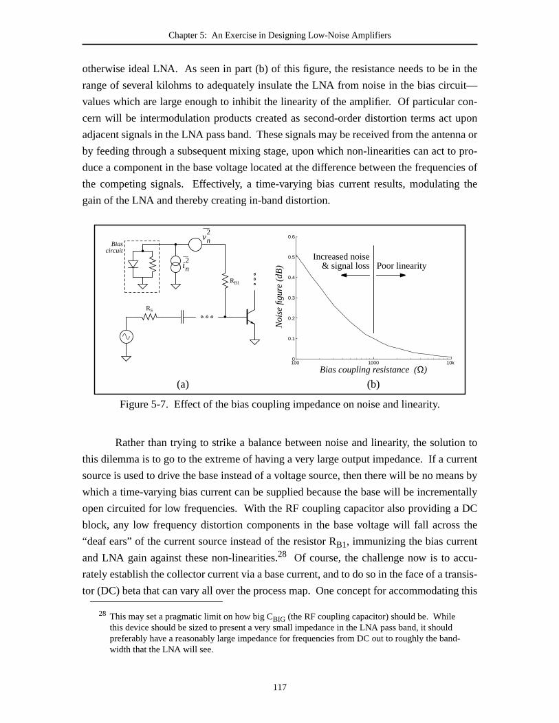
Chapter 5: An Exercise in Designing Low-Noise Amplifiers
n the
it—
on-
upon
nna or
pro-
cies of
the
n to
rrent
ans by
ntally
DC
the
-
ansis-
g this
d-
otherwise ideal LNA. As seen in part (b) of this figure, the resistance needs to be i
range of several kilohms to adequately insulate the LNA from noise in the bias circu
values which are large enough to inhibit the linearity of the amplifier. Of particular c
cern will be intermodulation products created as second-order distortion terms act
adjacent signals in the LNA pass band. These signals may be received from the ante
by feeding through a subsequent mixing stage, upon which non-linearities can act to
duce a component in the base voltage located at the difference between the frequen
the competing signals. Effectively, a time-varying bias current results, modulating
gain of the LNA and thereby creating in-band distortion.
Rather than trying to strike a balance between noise and linearity, the solutio
this dilemma is to go to the extreme of having a very large output impedance. If a cu
source is used to drive the base instead of a voltage source, then there will be no me
which a time-varying bias current can be supplied because the base will be increme
open circuited for low frequencies. With the RF coupling capacitor also providing a
block, any low frequency distortion components in the base voltage will fall across
“deaf ears” of the current source instead of the resistor RB1, immunizing the bias current
and LNA gain against these non-linearities.28 Of course, the challenge now is to accu
rately establish the collector current via a base current, and to do so in the face of a tr
tor (DC) beta that can vary all over the process map. One concept for accommodatin
28 This may set a pragmatic limit on how big CBIG (the RF coupling capacitor) should be. Whilethis device should be sized to present a very small impedance in the LNA pass band, it shouldpreferably have a reasonably large impedance for frequencies from DC out to roughly the banwidth that the LNA will see.
100 1000 10k 0
0.1
0.2
0.3
0.4
0.5
0.6
(a) (b)
Biascircuit
RB1
RS
Figure 5-7. Effect of the bias coupling impedance on noise and linearity.
Bias coupling resistance (Ω)
No
ise
fig
ure
(d
B) Increased noise
& signal loss Poor linearityin2
vn2
117

Chapter 5: An Exercise in Designing Low-Noise Amplifiers
the
re
ce
ro-
dying
upply
gain
cur-
omi-
flow
base
ly
cir-
r of
variation is portrayed in Figure 5-8. Transistors Q1 and Q2 form a∆VBE pair through
which the currents are forced to match by the mirror MP1-2. Under this condition,
base-emitter voltages of Q1-2 differ by an amount , whe
the ratio is equal to the device layout multiple . This potential differen
falls across the resistor RBIAS, creating a supply-independent reference current that is p
portional to absolute temperature (PTAT)—characteristics that are desirable for stea
the gain and input match of the LNA over operational changes in temperature and s
voltage. The next addition to the circuit is Q3, which provides a measure of current
to reduce the base current induced error betweenIC1 and IC2. But instead of tapping
directly into the supply, the base drive being furnished by Q3 is first passed through a
rent sensing device—the diode-tied MP3. Assuming that the NPN base current is d
nated by the reverse injection of holes from the base into the emitter, Q1 and Q2 will
equal base currents despite the difference in emitter area, giving .29 Then,
when matched to Q1, the LNA common-emitter input transistor will have the same
drive requirements, allowingIC1 to be replicated in the LNA stage by appropriate
ratioing a current source device slaved to MP3. By way of saving power in the biasing
cuitry, the reference device Q1 is scaled down from the LNA transistor by a facto
29 Reverse injection is the predominant source of base current in silicon homojunction and SiGegraded-base transistors. This will generally not be true for HBTs, with which some beta-compensation resistors in the base leads of Q1 and Q2 may be required.
∆VBE kT q⁄( ) I S2 I S1⁄( )ln=
I S2 I S1⁄ m 4=
Start-upcircuit
Q2
Q3
m=1Q1
m=1MP3 MP4
MP1 MP2
RBIAS
m=4
m=14
IBASE
Figure 5-8. Concept for the base current source bias scheme.
I DP3 2I B1=
118

Chapter 5: An Exercise in Designing Low-Noise Amplifiers
in
will
e
hich
ver,
ation
in
ut in
allow
bias
As
r cur-
put
high
sistors
are
itter
hem-
con-
esis-
e little
n/off
tran-
6)
n-
; the currentIBASEthus needs to be similarly larger thanIC1, and can be delivered
by sizing the current source MP4 relative to MP3 as a device multiple of .
Fleshed out in slightly more detail, the complete solution is presented
Figure 5-9. At room temperature (taken to be 300K), the base-emitter voltage of Q1
be 36mV larger than that of Q2, so 370Ω for RBIAS sets the current in each side of th
∆VBE cell to about 100µA. The emitter of Q1 is drawn at 0.5µm by 1.8µm to be approx-
imately a factor of 28 smaller than the common-emitter LNA transistor, a geometry w
will not provide the best possible transistor matching.30 Unfortunately, constructing the
LNA device as 28 unit copies of Q1 would compromise its RF performance. Howe
being that the absolute value of the LNA bias current is already subject to the fabric
tolerances in the resistance of RBIAS, trying to match transistors to better than one part
ten would be a futile effort anyway. The same thinking runs behind the relaxed layo
sizing the p-channel current sources relative to the sensing device MP3. Then, to
compensation for process variations, an external trim is incorporated by way of a
adjustment pin. Applying a voltage to this pin effectively alters the value of RBIAS by sub-
stituting for some of the current flowing into the resistor or pulling more through Q2.
one example, shorting thebias_adj pin to ground lowers RBIAS from 370Ω to 270Ω(370Ω in parallel with the 1kΩ of RADJ). To use the “default” (nominal) bias condition in
the LNA,bias_adj may simply be left floating.
Support for the low power mode is easily accomplished by appending anothe
rent source device (MP5) to MP3 along with a set of switches (MN1-4). The digital in
lna_ctl is provided as a means of selection, where applying a logic high activates the
performance mode and a logic low chooses the low power stage using the pass tran
MN3-4. Serving to pull the base of the off-state input device (weakly) toward ground
MN1-2, where a high resistance pull-down is actually preferable so that the base-em
junction capacitance of the off transistor does not load the input. For the switches t
selves, the choice was to minimize the capacitance on thebiashandbiasl nodes so as to
not shunt the current sources at 5.8GHz. Although p-channel devices would likely
tribute less noise and would also offer the possibility of further increasing the output r
tance by biasing them as cascode transistors, these effects were deemed to provid
additional benefit in this design and thus smaller n-channel switches with simplistic o
biasing were used. The remaining need in the LNA signal path is to bias the cascode
sistors, for which a 2VBE reference is produced by supplying some current (via MP
30 The emitter area ratio used in the design is actually a little more than 28. This helps to compesate for the resistance of the emitter inductor used in the LNA stage.
m 28=
m 14=
119

Chapter 5:
An E
xercise in Designing Low
-Noise A
mplifiers
120
MP47x10µ/5µ
MP57x10µ/5µ
m=4 m=1
MN32x5µ/1µ
MN42x5µ/1µ
MN12µ/2µ
MN22µ/2µ
lna_ctl lna_ctl
lna_
ctl
lna_
ctl
biaslbiash
cbiash
cbiasl
Hz LNA.
LM
Q1
Q3
MP3
MP1 MP2
RBIAS
Q2m=4m=10.5µx1.8µ 0.5µ x1.8µ
0.5µ x2µ
Q50.5µx2.5µ
0.5µx2.5µQ4370Ω
RADJ
1kΩ
2 x 10µ/5µ
20x10µ/5µ20x10µ/5µ 20x10µ/5µ
MP92x10µ/5µ
MP82x10µ/5µ
MP7 MP620x10µ/5µ
MP102µ/10µ
CBYP
3.9pF
bias_adj
Figure 5-9. Biasing circuitry for the switched-stage 5.8G

Chapter 5: An Exercise in Designing Low-Noise Amplifiers
and
e of
s
ignal
con-
se of
thus
es of
rcuit
ltage
P8;
ows
era-
is
he
cheme
hown
ers
se fig-
t
e
int--
through Q4 and Q5. A switch arrangement similar to MN1-4 selects the active stage
provides a pull-down for the other. Having already noted the relative independenc
LNA noise performance and gain to VCE, the 2VBE common-base reference level i
geared toward maximizing the supply headroom available at the collector node for s
swing. Given the high impedance at this node, available swing range will be the key
spirator in gain compression.31
Together with the current mirror MP1-2, the∆VBE cell (Q1-2) forms a regenera-
tive bias circuit for which a zero current condition is also a stable state. When the ba
Q3 is low and the gate bias on MP1-2 is at supply, then no current will be drawn and
no gain resides in the circuit from which to escape the zero state. For the purpos
facilitating the transition out of this state at power-up, MP7-10 comprise a start-up ci
that initializes some current into the regenerative quad. As soon as the supply vo
exceeds two p-channel device thresholds, MP10 will begin pulling current through M
this current in turn is mirrored into the regenerative bias cell by MP9. Once current fl
in the∆VBE pair, MP7 will tie off the MP8-9 current mirror as the 100µA it sources will
easily overpower the (approximately) 10µA availed by MP10.32 The factor of 10 in mar-
gin should ensure reliable shutdown of the start-up circuit over all variations in temp
ture, supply, and process.33
Any way it is sliced, this bias circuit entails a lot of transistors; that this circuit
going to be used to power alow-noiseamplifier may appear to have been forgotten in t
design process. However, the high impedance furnished by the current source bias s
should isolate the signal path from this gadgetry, a promise borne out in the results s
in Figure 5-10 of simulating the entire LNA design. By comparison with the numb
obtained using the ideal sources (last seen in Figure 5-6), it is observed that the noi
31 The 1dB (gain) compression point is a common metric of linearity and relays the signal powerlevel at which the gain supplied by the device to a single input tone has fallen by 1dB from itssmall-signal limit. Care should be taken in reading this measure as to whether it is referring tothe input or output signal level at which the 1dB of gain compression is observed.
32 While the start-up injection into the∆VBE pair is turned off, the current drawn through MP10 isnot. Under worst-case conditions (e.g., -40C, 5V supply, fast p-channel devices), the quiescencurrent in the start-up circuit can rise to 50µA. Although this is a fairly small overhead com-pared to the milliamps of current flowing in the LNA, this may not be case in all circuits forwhich the use of a regenerative biasing circuit is considered.
33 For the technology-conscious, this base current source biasing circuit makes use full use of thtrappings of a BiCMOS process. In fact, it could be implemented using only bipolar devices;many bipolar processes offer lateral PNPs which can replace each p-channel MOSFET used this design with the exception of the “resistor” MP10. Switching between modes becomes a litle more complex, and may best be accomplished by providing the base drive for the base current source transistors through switched emitter-followers rather than trying to use bipolardevices as a pass transistors.
121

Chapter 5: An Exercise in Designing Low-Noise Amplifiers
s been
in the
ain
idth
ode
r than
t full
nents
ure (in the high performance mode) has crept up a mere 0.06dB and that the gain ha
taxed less than 1dB. The final numbers are 13dB of gain and a 2.3dB noise figure
8mW high performance setting, while the 2mW low power mode provides 8dB of g
and an 8dB noise figure. Input return loss is better than 14dB for a 200MHz bandw
about 5.8GHz; looking at the output, the return loss is at least 7dB in the low power m
and 12dB when high sensitivity is being demanded. In either case, isolation is bette
22dB for frequencies anywhere near the band of interest. These numbers reflec
device-level simulations including all parasitics associated with the passive compo
and pads, and have been gauged with real-world 50Ω source and load impedances.
5.4 5.5 5.6 5.7 5.8 5.9 6 6.1 6.2−30
−24
−18
−12
−6
0
5.4 5.5 5.6 5.7 5.8 5.9 6 6.1 6.2−30
−28
−26
−24
−22
−20
5.4 5.5 5.6 5.7 5.8 5.9 6 6.1 6.2−30
−28
−26
−24
−22
−20
5.4 5.5 5.6 5.7 5.8 5.9 6 6.1 6.2−30
−24
−18
−12
−6
0
5.4 5.5 5.6 5.7 5.8 5.9 6 6.1 6.2−30
−28
−26
−24
−22
−20
5.4 5.5 5.6 5.7 5.8 5.9 6 6.1 6.2−30
−28
−26
−24
−22
−20
5.4 5.5 5.6 5.7 5.8 5.9 6 6.1 6.25
6
7
8
9
5.4 5.5 5.6 5.7 5.8 5.9 6 6.1 6.2
4
6
8
10
5.4 5.5 5.6 5.7 5.8 5.9 6 6.1 6.2
4
6
8
10
5.4 5.5 5.6 5.7 5.8 5.9 6 6.1 6.22
2.2
2.4
2.6
2.8
5.4 5.5 5.6 5.7 5.8 5.9 6 6.1 6.2
10
11
12
13
14
5.4 5.5 5.6 5.7 5.8 5.9 6 6.1 6.2
10
11
12
13
14
Frequency (GHz) Frequency (GHz)
Ga
in (
dB
)
(a) (c)
NF50
NFmin
Ga
s21
NF50
NFmin
Gas21
Figure 5-10. Simulated performance of the 5.8GHz switched-stage LNA inboth the (a,b) “high performance” and (c,d) “low power” modes. Note thescale change between the modes in representing the gain and noise figure.
No
ise
fig
ure
(d
B)
Ga
in (
dB
)
No
ise
fig
ure
(d
B)
“High performance” mode “Low power” mode
Frequency (GHz)(d)
Frequency (GHz)(b)
Iso
latio
n (
dB
)
Re
flect
ion
ga
in (
dB
)Is
ola
tion
(d
B)
Re
flect
ion
ga
in (
dB
)
s12
s12s11
s11
s22
s22
122

Chapter 5: An Exercise in Designing Low-Noise Amplifiers
per-
ss
pro-
nce;
in rel-
z for
es
ith
with
endent
ria-
m.
i-
hip,
al
e-
ge
While the aforementioned set of simulations have rested on a 3V supply and o
ation at room temperature, the∆VBE bias cell should provide a high degree of robustne
in the operation of the LNA should these conditions change. The essence of gain is
portional to gm, as are terms in the real and imaginary components of the input impeda
keeping the transconductance constant, the insertion gain and input return loss rema
atively unaffected by temperature as reflected in Figure 5-11(a). Calculated at 5.8GH
a temperature range of -40 to 100°C, gain droops only slightly at elevated temperatur
and curls up marginally toward the extremes. Following suit in Figure 5-11(b) w
supplies ranging from 2V to 5V, the LNA gain witnesses only a slender increase
higher voltages and the return loss remains high despite the presence of voltage-dep
junction capacitances.34 Such independence, from both supply and temperature va
tions, will go a long way in preserving the integrity of the RF link in a portable platfor
5.1.4 Layout Design of the 5.8GHz Switched-Stage LNA
Having been convinced that the LNA circuits are fulfilling the obligations orig
nally set forth, attention now turns toward the layout. A die photo of the finished c
measuring 1.34mm by 1.18mm,35 is furnished in Figure 5-12. Placement of the five spir
34 Though measured at the 5.8GHz band center for the purposes of this illustration, this is at a frquency where is quite high, not at the minimum in . This selection of frequen-cies exacerbates the extent to which the return loss is actually changing; temperature and voltacoefficients—particularly in the junction capacitances—actually result in a slight shift in thecenter frequency.
35 The chip is this size, the die photo is somewhat larger.
s11
s11∂ f∂⁄ s11
2 2.5 3 3.5 4 4.5 5
11
12
13
14
15
2 2.5 3 3.5 4 4.5 5−20
−18
−16
−14
−12
−40 −20 0 20 40 60 80 100
11
12
13
14
15
−40 −20 0 20 40 60 80 100−20
−18
−16
−14
−12
Temperature (°C) Supply voltage (V)
Ga
in (
dB
)
(a) (b)
s21s21
Figure 5-11. Simulated behavior of the 5.8GHz switched-stage LNA over(a) temperature and (b) supply variations.
Re
flect
ion
ga
in (
dB
)
Re
flect
ion
ga
in (
dB
)
s11
s11
Ga
in (
dB
)
123

Chapter 5: An Exercise in Designing Low-Noise Amplifiers
s the
ing
ned
n, an
pper
duc-
the
inductors, each sitting above a grid of deep trench isolation pockets, largely dictate
floorplan as an exercise in minimizing inter-spiral coupling. From the left, and mov
counterclockwise, the inductors can be identified in the die photo as LB, LE, LDC, LE2, and
LC. With the exception of the DC bias path inductor LDC, each spiral consists of the top
two metal levels strapped together using copious amounts of vias.36 For LDC, as its pri-
mary goal is to be invisible from an RF perspective, a multi-level winding is desig
instead. Composed of a last metal trace that spirals inward in a clockwise fashio
array of vias reaching down two levels, and then a metal 3 winding that mirrors the u
spiral but continues the clockwise direction, this multi-level arrangement increases in
tance by creating (positive) mutual coupling vertically as well as laterally. Each of
input matching inductors (LB, LE, and LE2) are optimized for quality factor using wide
metal traces, while narrower line widths are adopted in LC and LDC where Q is not as
important. Were it not for these differing considerations, inductors LE2 and LDC might
conceivably be jointly realized as one tapped spiral.
36 The sets of vias can actually be seen in the photo as the darkened “blotches” in the spirals.
Figure 5-12. Die photo of 5.8GHz switched-stage LNA IC (CMLNA-SW).
124

Chapter 5: An Exercise in Designing Low-Noise Amplifiers
and
e RF
er
aving
are:
put
he
sign so
pads
sical
ional
tely
mid-
s the
arious
ent in
ugh
ne of
he
nce
uctors,
real-
ty is
h an
ven
citing
ed—
these
tes-
Next in order of conspicuousness are the pads, with the RF input (on the left)
output (on the right) designed for contact by coplanar waveguide GSG probes. Th
pads transition to a 50Ω microstrip arrangement with a last metal signal trace over a low
metal ground plane. Along the bottom is a set of pads for a bypassed supply probe h
four power pins interspersed with three grounds. The power pins, from left to right,
the LNA supply voltage, the bias circuit supply voltage, the LNA mode select in
(lna_ctl), and thebias_adjpin. The LNA signal path and the bias circuit operate from t
same voltage and could share a supply, but have been given separate pins in this de
that the currents can be individually measured. ESD protection is provided near the
in the form of clamping FET devices between the supply pins and ground, plus a clas
double diode, series resistor scheme for the digital mode select input.37 The remaining
pin, bias_adj, already feeds into resistors and the emitter of an NPN, and so no addit
precautions were taken.
Sitting in the lower-left corner is the bias circuit, where it occupies approxima
the same amount of area as one of the spiral inductors. The big chunk of metal in the
dle of the chip forms the shared top (ground) plate of the capacitors that bypas
common-base bias voltages; other supply-filtering capacitances are added in at v
locations throughout the chip where space and convenience allow. Finally, as evid
the upper-right corner, the name CMLNA-SW has been affixed to this design. Tho
having no feasible pronunciation, the first part of the acronym identifies this chip as o
the C-band Monolithic Low-Noise Amplifiers. The SW suffix specifically calls out t
switched (bipolar) version to differentiate it from the CMOS implementation.
In the final tally, the addition of a low power mode that protects the impeda
matches, sustains isolation, and provides some gain has come at a cost of two ind
0.25dB in noise figure, and about 5dB of gain. In exchange, however, this allows a
time option of reducing the power consumption by a factor of four when peak sensitivi
not required of the receiver. Beginning with the 1.5dB NFmin and the 15.5dB Gma exhib-
ited by this 0.5µm graded-base bipolar technology at 5.8GHz, this design finished wit
LNA featuring a noise figure 0.8dB higher and an insertion gain about 2.5dB lower (e
after cascoding) than the intrinsic device measures. It should be remembered in
these results that inductor quality factors in the high teens (17-19) have been assum
numbers which are about the best that could be expected in a silicon technology at
37 The FETs intended for clamping ESD transients are some fairly wide n-channel devices thathave been ruggedized with a larger drain region and by adding some resistance between the gaterminal and ground. Negative transients are clamped by the drain to substrate diode, while poitive transients turn on the transistor by coupling energy from the drain to the gate via CGD [66].
125

Chapter 5: An Exercise in Designing Low-Noise Amplifiers
xplo-
ding
out
iasing
nsis-
and
l argu-
nduc-
id for
the
r
the
t
this
(e.g., a
NPN).
l, can
he
and
all by
,
-
-
frequencies. Nonetheless, these metrics will be useful to keep in mind during the e
ration of using CMOS as an alternative.
5.2 CMOS LNA Design
Notwithstanding the dramatic appearance of CMOS transistors in the prece
section, a rather bipolar-centric view into the world of LNAs have prevailed through
this presentation. Lest CMOS be relegated to the vagaries of behind-the-scenes b
duties, it should be emphasized that the small-signal models of bipolar and CMOS tra
tors are essentially the same—particularly at RF frequencies where Cπ dominates the
base-emitter junction impedance. The differences really only reside with the values
dependencies of the model parameters; as such, the topological and technologica
ments made in the context of bipolar designs also apply here. To be sure, the transco
tance of CMOS transistors is lower for any given bias current, and the same can be sa
the output resistance.38 But so too are most of the device capacitances, perhaps with
notable exception of the gate-drain capacitance (CGD), which tends to be of the same orde
as Cµ in RF-sized transistors. By way of terminal resistances, that encountered in
extrinsic source-drain regions is usually around 500Ω-µm for n-channel devices and abou
a factor of three higher for their p-channel brethren [67]. In symmetric MOSFETs,
resistance can be assumed to split equally between the source and drain terminals
100µm wide n-channel transistor will be encumbered by 2.5Ω of extrinsic source resis-
tance, a number in the same ballpark as the emitter resistance of a reasonably-sized
Resistance in the gate terminal, although distributed across the width of the channe
be modeled for noise, delay, and fMAX purposes by a single lumped resistor taking on t
value [68]:
, (5.8)
where represents the sheet resistivity of the gate material (polysilicon or silicide)
n is the number of gate fingers. The gate resistance can readily be made fairly sm
using multiple finger layouts; revisiting the example of the 100µm wide device, assuming
a 0.5µm (drawn) channel length and a silicided poly layer having a resistivity of
a layout with 10 gate fingers would exhibit 3Ω of gate resistance. So, at least in the com
38 Transistor output resistance is probably not too compelling an issue in RF applications as impedances tend to be limited by inductor loss anyway. As further evidence, there are certainly plentyof MESFET and HEMT devices to be found in microwave and mm-wave designs.
RG13---R
WnL------
=
R
4.5Ω ⁄
126

Chapter 5: An Exercise in Designing Low-Noise Amplifiers
nsis-
issue,
cess.
polar
l noise
ter for
resis-
ources
shot
pos-
re-
ems
ces a
FETs
RF
the
nnel,
ltage
].
parison of terminal parasitics, CMOS devices stack up quite well against bipolar tra
tors. As will be seen next, however, noise is another matter altogether.39
5.2.1 Noise in CMOS Transistors
Regardless of the chosen device technology, when noise is the substantive
having a solid understanding of its various origins is the cornerstone of the design pro
Fortunately, the similarities observed earlier between the small-signal models for bi
and CMOS transistors also extend to the presence of noise sources. The therma
from the terminal resistances is treated exactly as discussed in the previous chap
bipolar devices, even though the effects of geometry and process scaling upon the
tances may differ. There are also analogues to the base and collector current noise s
observed in bipolar transistors, although the mechanism is considerably different as
noise processes—classically speaking—do not occur in MOSFETs.40 Instead, thermal
agitations vary the velocity of the carriers in the channel, lending a noise component
sessing the power spectral density:
(5.9)
to the drain current which is proportional to the zero-bias drain conductance (gd0) of the
device. In the long-channel limit,gd0 simply equals the transconductance, but can app
ciably exceed gm in shorter channel transistors. Similarly, as measured drain noise se
to outpacinggd0 in modern technologies, the “excess noise” factorγ can be significantly
inflated beyond the value of 2/3 observed at long channel dimensions.41
Charge in the channel, as mirrored across the oxide capacitance, also indu
noise current in the gate. The presence of an induced gate current was recognized in
by van der Ziel in the 1960s [69][70], but that it is of consequence for the design of
amplifiers in CMOS has only fairly recently been remembered [71]. Resulting from
finite transit time carriers require in getting from the source into and through the cha
the phase of the input current undergoes a shift relative to the gate-to-source vo
39 With all apologies to Jim Abrahams, the Zucker brothers, and the rest of the creative crewresponsible for foisting theAirplane movies into our collective conscience: “As will be seennext, however, noise is another matter.”
40 This may not be entirely true, particularly for highly scaled CMOS transistors. Ballistic trans-port in the channel [72] and gate leakage current [73] both lead to the presence of shot noise.Furthermore, some argue that channel noise in subthreshold might have shot noise origins [61
41 Clear explanations behind this increase are still being sought. Much like an effective mass,many of these noise “factors” are essentially the right answer divided by the wrong answer,where the “right” answer is the measured result and the “wrong” answer is that calculated fromconventional physics models.
iD2
4kTγgd0=
127

Chapter 5: An Exercise in Designing Low-Noise Amplifiers
onfer-
d by
ives
gate.
ima-
s to
s are
in that
in the
-
nnel
ame
case
ough a
e cor-
ter.
noise
base
teer
, and
tice,
hich
ure.
ot
applied to a MOSFET. This phase shift becomes noticeable at higher frequencies, c
ring upon the FET a real component in the input impedance that can be modele
placing a gate conductance:
(5.10)
in parallel with CGS. Fluctuations in the channel charge, and thus in the delay which g
rise to this conductance, are also responsible for the noise current flowing into the
The gate noise has an associated power spectral density:
, (5.11)
whereδ is the excess gate noise factor. Applying the classical long-channel approx
tions renders a value of 4/3 forδ, although short channel transistors have played witnes
an exacerbation of this effect as well. While both the gate and drain noise current
rooted in the same charge flow mechanism, these terms are only partially correlated
they have different dependencies upon the location of a given noise disturbance with
potential distribution along the length of the channel.42 Conventional models peg the cor
relation coefficient at , but as the lengths within the devices shrink, the cha
position dependencies converge and the degree of correlation increases.
Equivalent input noise generators can be derived for MOSFETs in much the s
fashion as performed for bipolar transistors. Some care must be taken in the CMOS
to manage the correlation between the drain and induced gate noise sources, alth
reasonable first-order cut at noise behavior can be obtained merely by substituting th
responding terminal identifiers into the relationships expressed in the previous chap43
The real danger in omitting from the design process is that doing so leads the
optimization astray. Just as would be the case with bipolar transistors were there no
shot noise (or if the current gain was infinite), the goal of minimum noise would s
toward the use of vanishingly small devices biased at correspondingly small currents
then compensating for the gain using a high Q input matching network. But in prac
this matching network would present a large source impedance to the FET through w
the gate noise current would flow, saddling the amplifier with a sub-optimal noise fig
42 A nice graphically-reinforced derivation of the differences between the induced gate and drainnoise currents can be found in a thesis by Sepke [74].
43 This should not come across as being completely heretical as the base and collector current shnoise sources in bipolar devices are also partially correlated [75]. However, the correlation inbipolar transistors is routinely ignored for frequencies below fT.
gg
ω2CGS
2
5gd0-----------------=
iG2
4kTδgg=
c j0.395=
iG2
128

Chapter 5: An Exercise in Designing Low-Noise Amplifiers
carna-
f the
5
SFET
This
n
ome
re
ance:
nput
se
soci-
in the
ted by
i-
ence a
e
.2 and
eters.
Unfortunately, the absence of gate noise is exactly the scenario professed by most in
tions of CMOS circuit simulation models to date.
After determining that induced gate noise was responsible for the departure o
measured noise figure from their expectations for a 1.5GHz LNA design (in a 0.3µm
process), Shaeffer and Lee have suggested a revised noise analysis of tuned MO
amplifiers, offering [71][76]:
(5.12)
as a more complete description of the noise factor for a common-source transistor.
definition provides a value for F intermediate between F50 and Fmin, as it assumes that the
RF source (having an output resistanceRs) is reactively matched to the device through a
inductance LG added before the gate terminal. This inductor may come attached to s
series resistance ( ), which will directly add to the gate terminal resistance (RG) com-
ponent defined in Equation 5.8. The ratio refers to the drain noise current, wheαindicates the extent to which the transconductance falls short of drain conduct
. Noise and loss in the input circuit is reflected through its quality factor:
, (5.13)
which also equals the voltage transformation ratio (voltage gain) provided by the i
matching network at resonance. Finally, theχ parameter brings the induced gate noi
into the noise factor expression as:
, (5.14)
whereδ andc respectively are the excess noise factor and correlation coefficient as
ated with the gate noise current. The one remaining piece that should be included
analysis is the extrinsic source terminal resistance, which can easily be accommoda
lumping it together withRG in Equations 5.12 and 5.13.
Now, what remains is to determine Fmin by finding the source resistance that min
mizes the noise factor expression provided above. For a chosen device size (and h
given CGS), this task is equivalent to locating the optimumQin. As a representative cas
study, a minimum-length n-channel MOSFET in a 0.5µm technology will be featured,
assuming the gate and extrinsic source resistivities are as exemplified in Section 5
that the long-channel approximations apply reasonably well to the noise param
F 1RLG
RG+
Rs----------------------
γα--- χ
Qin-------- f
f T------+ +=
RLG
γ α⁄
gm αgd0=
Qin1
2πf Cgs Rs RG RLG+ +( )
----------------------------------------------------------=
χ 1 2 c Qinδα2
5γ---------
δα2
5γ--------- 1 Qin
2+( )+ +=
129
Chapter 5: An Exercise in Designing Low-Noise Amplifiers
eter-
r an
ls
imu-
bers
vior are
ay-
-
se in
So,
sign.
lity
r cap-
rrent.
by
count
as
basic
ive an
that
nite
mum
—
-
red
Selecting a transistor gate width of 134.2µm—split into 22 gate fingers of 6.1µm each—
and a drain current of 5mA, the optimum source resistance for 5.8GHz operation is d
mined to be 91Ω (Qin of 1.8), at which point NFmin is 1.82dB.44 Reducing the drain cur-
rent in this device to 1.67mA increases the minimum noise figure to 2.52dB, found fo
of 89Ω. By way of providing some insight into how well the BSIM3v3 mode
available for this CMOS technology might compare, the same two bias points are s
lated using the commercial tool Spectre®, the results of which are plotted below in
Figure 5-13. Interestingly, the simulator model returns higher noise figure num
despite the absence of an induced gate current mechanism. Reasons for this beha
not clear, but it is believed that some of the additional transistor parasitics (e.g., CGD)
incorporated into BSIM3v3—and left out of the analytical Shaeffer work—might be pl
ing a significant role at this frequency.45 Also surprising, and difficult to fathom as con
forming to the actual device characteristics, is that the BSIM model predicts an increa
the minimum noise figure of only 0.1dB as the bias current is cut by a factor of three.
uncertainty persists, but this is the best information available for purposes of this de
The “guess” here is that the BSIM model is probably not terribly far removed from rea
for higher bias points at these device sizes, but then the Shaeffer development bette
tures the dependencies of the noise performance on transistor width and drain cu
Effectively, a linear mental construct will be employed where the y-offset is supplied
BSIM and the slope is taken from the analytical analysis. Neither model seems to ac
for all of the pertinent effects, but such is the quandary of IC design.
5.2.2 A 5.8GHz CMOS LNA
Despite the differences in the manifestation of noise within CMOS devices
compared to bipolar, the process for designing an LNA in CMOS is the same. The
approach was outlined in Chapter 4, where the first step is to size the transistor to g
of 50Ω.46 One of the key differences between the technologies, however, is
reaching this goal may not be feasible with CMOS given the bound of (reasonably) fi
power consumption. Recalling the example in the previous section wherein the opti
source resistances were in the 90Ω range, it is apparent that a considerably larger device
44 Establishing both the device size and the drain current sets the transistor fT as applied toEquation 5.12. This is a slightly over-constrained version of the problem Shaeffer and Lee formulate as the fixed gm optimization [76].
45 Gate terminal resistance is not included in BSIM3v3 either, but is added into the simulation byusing a subcircuit representation for the MOSFETs.
46 More generally, it should be said that the idea is to achieve a noise match by sizing the transistoto give an optimum source resistance that matches the output resistance of the source; this nenot be 50Ω.
Rsopt
Rsopt
130

Chapter 5: An Exercise in Designing Low-Noise Amplifiers
noise
for
ower
the
ltage
to
is rel-
ving
eing
r the
tor
r
operated at correspondingly higher drain currents—would be required to obtain a
match to a 50Ω source. In light of this limitation, a better design approach is to solve
the minimum noise figure (via Equation 5.12) that can be achieved given a fixed p
constraint. Optimizing under this condition finds the transistor width that furnishes
lowest noise while keeping constant the product of the drain current and the gate vo
required to support this current.47 As long as the channel is not driven too deeply in
inversion (i.e. the amount by which the gate-to-source voltage exceeds the threshold
atively modest), a fairly broad minima exists around an input matching network ha
—a solution that covers a reasonably wide range in the power dissipation b
tolerated of the design [76]. Using this result, and ignoring parasitic resistances fo
purposes of this calculation, Equation 5.13 recommends a CGS of 144fF for a 5.8GHz
amplifier. Then, given a 0.5µm technology having a gate oxide capacitance (Cox) of
3.9fF/µm2, the usual relationship suggests an optimum transis
width of 111µm. This is close to the width of 134.2µm chosen for this design, a numbe
arrived at through a slightly different set of approximations.48 Reapplying the Shaeffer
47 Increasing the device width lowers the required Von (gate overdrive potential) for a given draincurrent (ID), but in turn necessitates a larger ID to maintain the transistor fT. Somewhere in thisrelationship the optimum balance is struck.
48 Lee [77] provides a 750µm-GHz rule of thumb for the optimum transistor width, then observesthat variations of 20% about this number typically lead to degradations of only 0.1-0.2dB.
5 5.2 5.4 5.6 5.8 6 6.2 6.4 6.61.6
1.8
2
2.2
2.4
2.6
2.8
3
Figure 5-13. Comparison of models for the minimum noise figureof a common-source transistor at two drain current levels. Solid
lines represent results of the Shaeffer model [76] and dashed linesare simulation results using full BSIM3v3 models.
Frequency (GHz)
NF
min (
dB
)
Shaeffer modelID=5mA
Shaeffer modelID=1.67mA
BSIM modelID=5mA
BSIM modelID=1.67mA
Qin 3.8≅
CGS 2 3⁄( )WLCox=
131

Chapter 5: An Exercise in Designing Low-Noise Amplifiers
res
set-
con-
same
seen
of the
drain
e the
g
that
es.
cur-
model to this device with a 50Ω source resistance, the reactively-matched noise figu
are 2.01dB for the higher sensitivity (5mA) mode and 2.74dB for the reduced power
ting (where ID is 1.67mA). Judging from these numbers, it appears that the power
straint has cost between 0.2dB and 0.25dB in noise performance.
Forming the LNA around this device, a cascode transistor is appended for the
arguments made previously in light of the switched-stage implementation. As can be
in Figure 5-14, the geometry of the cascode was selected so that the interconnection
two transistors could be accomplished by merging the appropriate source and
regions. An inductance of 0.43nH is used in the source of the lower device to mov
input impedance to the 50Ω circle, from which point the match is completed by addin
another 2.4nH before the gate. The output matching network follows directly from
used in the bipolar design, where the same inductor (designated LD in this case) has been
used to facilitate comparisons in the performance of bipolar and CMOS technologi49
As the input capacitance of a MOSFET is only a weak function of the transistor bias
49 This design choice allows a more direct comparison of the gains exhibited by the CMOS andbipolar LNAs, without having to worry about differences in the signal power dissipated in theoutput matching network.
LM
LM
LD
2.7nH
LS
0.43nH
LG
2.4nH
C1
130fFC2
77fF
RB1
4kΩ
in
out
lna_bias
CBIG
LM/N+
LM/N+
MN122x6.1µ/0.5µ
21x6.1µ/0.5µMN2
Figure 5-14. RF signal path for the 5.8GHz CMOS LNA.
132

Chapter 5: An Exercise in Designing Low-Noise Amplifiers
while
The
f a
, this
been
nce
nd so
evel-
onduc-
upply
h to
ween
rela-
hich
ls of
-
s in
ce can
rent, a single stage suffices to meet the goal of maintaining an impedance match
allowing sensitivity and power consumption in the LNA to be traded for one another.
remaining piece is the 4kΩ bias coupling resistor; because the insulating gate o
MOSFET already provides an incremental open in the bias path at low frequencies
resistance will not lead to the linearity issues noted in the switched-stage design.50 This is
not to say that the concerns regarding noise contributions from the bias circuit have
alleviated in that this part of the picture painted in Figure 5-7 still holds; the impeda
presented by the FET will be matched to the RF source in the band of interest, a
having a large bias coupling resistance remains important. As an additional feature, d
oping a gate bias that compensates for temperature-induced variations in the transc
tance of the input transistor will prove handy, as is ensuring that changes in the s
voltage do not steer the LNA away from its intended bias current. The approac
addressing these challenges will provide another interesting set of parallels bet
designing with field-effect devices in comparison to bipolar transistors.
5.2.3 Stabilized Biasing for the CMOS LNA
One of the most salient characteristics of bipolar transistors is the exponential
tionship between the base-emitter voltage and the collector current, a relationship w
holds remarkably well over the transistor’s useful operating range. While the detai
establishing a current in CMOS are not as logarithmically clean, the∆VBE concept used in
biasing the bipolar LNA can similarly be applied to obtain a constant gm in an MOS tran-
sistor. The gate-source voltage is used instead of VBE, and the difference exhibited by two
MOSFETs flowing the same current can be expressed as:
, (5.15)
where the larger of the two devices is realized asm copies of the -sized smaller tran
sistor—a proportionality captured in the coefficient . When the current
each side of the∆VGS pair are equalized by a current mirror, a resistor (denoted RBIAS)
soaking up the difference in the gate-source potentials establishes a current:
, (5.16)
provided that an initialization mechanism ejects the circuit from the state.51 By
employing this current as a reference, the dependence of the transconductan
50 The linearity problems arise because of the base current in the bipolar transistors.
∆VGS cm
2I D
µCox------------ L
W-----=
W L⁄cm 1 m
1 2⁄––=
ID2
µCox------------ L
W-----
cm2
RBIAS2
--------------=
ID 0=
µCox
133

Chapter 5: An Exercise in Designing Low-Noise Amplifiers
ature
ich
ired
by
ply
hat
tivity
uum
ge
cur-
rst
rn
be cancelled in any MOSFET it serves to bias, taking the first-order source of temper
variation along with it.
This is the technique adopted for stabilizing the gain of the CMOS LNA, for wh
the gate bias is provided by the circuit drawn in Figure 5-15. Resistors RBIAS and RADJ
are sized in conjunction with the width of MN1 to conveniently establish the des
1.67mA and 5mA bias current levels in the LNA; the low power mode is enacted
leaving thebias_adjpin floating, and the high performance setting is chosen by sim
tying bias_adj to ground. The selection of two discrete operating modes is somew
arbitrary and is largely done as a matter of convenience; in practice, the sensi
afforded by this amplifier can be traded for lower power consumption along a contin
of points via thebias_adjpin. Completing the design—and ensuring that the volta
applied tobias_adjdoes not merely select among different values of zero for the bias
rent—is the start-up circuit formed by MP3 along with MN3-4. When power is fi
applied to the LNA, the gate of MN4 will be pulled high by the “resistor” MP3, in tu
drawing some current through the mirror MP1-2. Once the∆VGS cell reaches its destina-
51 Although the analysis provided here rests on the conventional square-law expressions forMOSFETs, the∆V concept should be applicable to virtually any transconductance device. Theresistance term appears squared because .gm I D∝
MP2 MP1
m=1m=8
10x20µ/2µ 10x20µ/2µMP32µ/25µ
MN23x6.1µ/0.5µ 3x6.1µ/0.5µ
MN1
RBIAS
830Ω
RADJ
830Ω
bias_adj
lna_bias2x10µ/2µMN3
5µ/2µMN4
LM
CBYP
1.7pF
Figure 5-15. Biasing circuitry for the 5.8GHz CMOS LNA.
134

Chapter 5: An Exercise in Designing Low-Noise Amplifiers
on
o-
Bor-
and
RF-
resen-
r-
espite
ed
tion current, MN3 will easily out drive MP3, thereby shutting off the kick-start injecti
supplied by MN4.
Although topologically different from the 5.8GHz design implemented with bip
lar devices, this entirely CMOS version has strived to achieve the same set of goals.
rowing the same 3V supply, the performance expected of the CMOS LNA at 15mW
5mW power consumption levels has been cast forth in Figure 5-16. Models for the
shielded pads and all of the passive devices have been included, while BSIM3v3 rep
tations are called upon for the MOSFETs.52 At 10dB, the gain observed in the high pe
formance setting is 3dB lower than that expected from the switched-stage design, d
5.4 5.5 5.6 5.7 5.8 5.9 6 6.1 6.2−30
−24
−18
−12
−6
0
5.4 5.5 5.6 5.7 5.8 5.9 6 6.1 6.2−30
−28
−26
−24
−22
−20
5.4 5.5 5.6 5.7 5.8 5.9 6 6.1 6.2−30
−28
−26
−24
−22
−20
5.4 5.5 5.6 5.7 5.8 5.9 6 6.1 6.2−30
−24
−18
−12
−6
0
5.4 5.5 5.6 5.7 5.8 5.9 6 6.1 6.2−30
−28
−26
−24
−22
−20
5.4 5.5 5.6 5.7 5.8 5.9 6 6.1 6.2−30
−28
−26
−24
−22
−20
5.4 5.5 5.6 5.7 5.8 5.9 6 6.1 6.23.5
3.75
4
4.25
4.5
4.75
5
5.25
5.4 5.5 5.6 5.7 5.8 5.9 6 6.1 6.2
4
6
8
10
12
5.4 5.5 5.6 5.7 5.8 5.9 6 6.1 6.2
4
6
8
10
12
5.4 5.5 5.6 5.7 5.8 5.9 6 6.1 6.23.5
3.75
4
4.25
4.5
4.75
5
5.25
5.4 5.5 5.6 5.7 5.8 5.9 6 6.1 6.2
4
6
8
10
12
5.4 5.5 5.6 5.7 5.8 5.9 6 6.1 6.2
4
6
8
10
12
Frequency (GHz) Frequency (GHz)
Ga
in (
dB
)
(a) (c)
NF50
NFmin
Ga
s21
NF50
NFmin
Ga
s21
Figure 5-16. Simulated performance of the 5.8GHz CMOS LNA in both the “highperformance” (a,b) and “low power” (c,d) modes. Noise figure calculations are bas
upon BSIM3v3 circuit models which have not implemented induced gate noise.
No
ise
fig
ure
(d
B)
Ga
in (
dB
)
No
ise
fig
ure
(d
B)
“High performance” mode “Low power” mode
Frequency (GHz)(d)
Frequency (GHz)(b)
Iso
latio
n (
dB
)
Re
flect
ion
ga
in (
dB
)Is
ola
tion
(d
B)
Re
flect
ion
ga
in (
dB
)
s12
s12
s11s11
s22
s22
135

Chapter 5: An Exercise in Designing Low-Noise Amplifiers
that is
polar
at a
te the
MOS
f
r loss
H for
-
: the
course,
ucing
ically
bout
ed to
g that
e. the
turn
rts (b)
ained
the
-sized
bipolar
rk for
r has
ss, the
l.s
e
the highest (drain) impedance an on-chip inductance can buy and a bias current
higher by nearly a factor of two—a testament to the higher transconductance of bi
transistors.53 With a 50Ω source resistance, the noise figure at 5.8GHz comes in
shade over 4dB, a number which is expected to be approximately correct—despi
absence of induced gate noise—as per the comparison in Section 5.2.1. While the C
LNA began with a 1dB poorer NFmin for the intrinsic device, another sizable portion o
the 1.7dB increase over the noise figure of the bipolar design occurs from the highe
associated with the larger total inductance needed to realize an input match (2.8n
versus 1.2nH for ).54,55 From this it may be concluded that if power con
sumption were not a consideration, the noise figure would improve on two fronts
larger transistor width would provide aΓopt closer to the 50Ω source resistance, and
would also necessitate less inductance to achieve an impedance-matched input. Of
power is a concern, which is why a 5mW setting has also been characterized. In red
the bias current by a factor of three, the gain would not be expected to fall too dramat
since—at best— ; as seen in the plots of gain, simulations predict a drop of a
2.5dB. Noise figure creeps up by about 0.75dB when the bias current is reduc
1.67mA, although the actual number may be another 0.5dB (or so) higher considerin
the induced gate noise has been neglected.
As the only device impedance that undergoes much of a change over bias (i.
output resistance) is effectively washed out by inductor loss, little is affected in the re
losses and isolation as the bias current is adjusted—a fact borne out in comparing pa
and (d) of Figure 5-16. Furthermore, all three measures should be similar to that obt
with the bipolar design, albeit each for different reasons. Isolation largely rests with
feedback capacitance and, as noted earlier, the gate-drain capacitance in an RF
CMOS device is about the same as the base-collector capacitance expected in a
transistor. The transformation ratio, and hence the Q, of the output matching netwo
each amplifier is predominantly set by the inductor loss, and the same spiral inducto
been used in both designs. On the input side, were the matching inductances lossle
52 Resistance in the gate terminal, as described by Equation 5.8, is added extrinsically.53 Recalling from Figure 5-6, it is worth noting again that the parallel stage design employed to
provide an input impedance match at two bias current levels cost the bipolar implementationabout 4.5dB in available gain.
54 Inductor quality factors in the high teens (at 5.8GHz) are being assumed in this design as wel55 The lower gain available from the CMOS transistors compared to the bipolar devices also take
a bite, increasing the noise penalty associated with adding the cascode. Contrary to what issometimes written, the noise of the cascode is reduced by Ga of the input transistor; however, thenoise of the cascode device is generally magnified by the high (and highly non-optimal) sourcimpedance it sees from the lower device.
LG LS+ LB LE+
gm ID1 2⁄∝
136

Chapter 5: An Exercise in Designing Low-Noise Amplifiers
-
tance,
idth.
NA in
less
oun-
the
ated
us-
have
pond-
t
pads
rn
he
-
MIM
this
o be
d for
olt-
g cir-
t
e gate
the
ng the
nner
CMOS LNA would have a higher Q impedance match due to CGS of the input device
being smaller than the corresponding Cπ term in the bipolar implementation. With on
chip spirals, however, the loss in the inductors tends to scale faster than the induc
and the higher loss experienced in the CMOS design acts to widen its input bandw
Regardless, if the numbers seen in these simulations are any indication, a 5.8GHz L
a 0.5µm CMOS technology appears quite usable for the types of wideband wire
applications being considered throughout this work.
5.2.4 Layout Design of the 5.8GHz CMOS LNA
Although a number of different technology-based limitations have been enc
tered along the way, the approach to designing an LNA in CMOS has mirrored
switched-stage effort in many ways. The layout of the IC is no exception; design
CMLNA-CM (the suffix indicates CMOS), the die photo that appears in Figure 5-17 ill
trates the striking resemblance. As the input impedance characteristics of MOSFETs
lent themselves to a single stage amplifier, there are two fewer inductors and a corres
ingly smaller 1.03mm by 0.96mm die area.56 Residing on the left side is the RF inpu
while the output is taken from the right, both of which make use of RF-shielded GSG
and on-chip 50Ω microstrip traces leading to and from the amplifier. Noting the 4-tu
spiral—in place of the 1.5-turn LB—encountered immediately after the input pads, t
larger matching inductance needed for LG is clearly evident. In helping to reduce cou
pling into the substrate, each of the inductors—as well as the poly resistors and
capacitors—is formed over a grid of the deep trench isolation pockets available in
technology.
Looming along the bottom of the photo is a set of pads that allows the chip t
powered from the same 4 power, 3 ground, bypassed supply probe which will be use
the switched-stage LNA. The far left and far right pads in this row furnish the supply v
age, where the pin farthest to the right provides a separate connection for the biasin
cuitry. Adjacent to this pin is thebias_adjcontrol, leaving the extra pad—freed by no
needing a separate mode select input—to be used as an off chip connection to th
voltage of the p-channel current mirror. Should the start-up circuit fail to initialize
regenerative bias cell, this pin can be stimulated as an alternative means of escapi
zero condition. The bias circuit itself is quite compact, fitting entirely inside a 170µm by
100µm rectangle. Finally, protection from ESD transients is included in the same ma
56 For the curious: yes, this die photo is shown (approximately) to scale relative to the switched-stage LNA.
137

Chapter 5: An Exercise in Designing Low-Noise Amplifiers
sup-
in
reater
t and
ence
lity
ice
med
nclu-
esign,
OS
f pas-
prescribed for the bipolar design, with extended drain MOSFETs placed between the
plies and ground and double diode clamps on the analog input.
Looking back, this LNA design began with a CMOS transistor having a Gma of
10.6dB and a 50Ω noise figure of 2.7dB within its reach, then finished with 10dB of ga
and a noise figure anticipated to be in the 4dB neighborhood.57 At least in terms of noise,
this would seem to suggest that the CMOS technology has been burdened to a g
extent (than the bipolar) in supporting the requisite degree of return loss at the inpu
output along with reasonable amounts of gain and isolation. The 1.3dB differ
between the “starting” and “ending” noise figures for the CMOS design is the “rea
tax”; in comparison, the bipolar version finished within 0.8dB of the intrinsic dev
NFmin. Hence, the additions required to turn a raw device into a useful LNA have see
to exacerbate the noise disparity between the two device technologies. While this co
sion has been based on the most complete information available at the time of the d
the question of salience for the design of wireless systems is: “Given bipolar and CM
technologies at the same lithographic node and providing the same accompaniment o
sive devices, what is the real difference in performance?” The answer comes next.
57 The achievable noise figure of 2.7dB is derived from the “linear mental construct” described inSection 5.2.1. The y-offset in this construct is the 2.5dB NFmin calculated from the BSIMmodel and shown in Figure 5-13; the slope portion is the 0.2dB penalty for failing to provide anoptimum noise match.
Figure 5-17. Die photo of 5.8GHz CMOS LNA IC (CMLNA-CM).
138
Chapter 5: An Exercise in Designing Low-Noise Amplifiers
the
itivity
n fab-
.5
ATN
scade
itors
to
ndard
auto-
50
the
o the
nal-
ance)
than
antly
king
ve
hion.
6dB
e dis-
pinned
mined
in the
, if
5.3 Measured Results for the 5.8GHz LNAs
Two 5.8GHz LNA designs have been completed, one entirely in CMOS and
other relying upon bipolar transistors. Both designs provide fully-integrated 50Ω in, 50Ωout solutions with on-chip biasing and a means of saving power when reduced sens
is permissible. To provide the most direct comparison possible, the designs have bee
ricated together, sitting beside one another on a set of wafers produced in a 0µm
BiCMOS technology. All characterization has been performed on wafer using an
noise measurement system in conjunction with an HP8510 network analyzer, Ca
Microtech AirCoplanar® GSG probes, and a DC probe card with 100pF bypass capac
located at each of the four power pins.With the RF pads having been incorporated in
the on-chip matching networks, no deembedding is performed on the measured data—the
measurement system is simply calibrated to the probe tips using an impedance sta
substrate. The setup from ATN also includes an HP8970B noise figure meter and an
mated tuner along with a set of isolators mounted at the probes to provide accurateΩnoise figure, minimum noise figure, andΓopt measurements.
First to come under the microscope is the switched-stage version, for which
noise figure and gain are reported in Figure 5-18. Both stages prove operational;58 the
high performance mode dissipates 8mW when provided a 3V supply, and switching t
low power setting reduces the power by a factor of four. Moving beyond these functio
ity checks, the first observation from the RF measurements finds the (high perform
noise figure and gain characteristics centered around 5.1GHz—about 12% lower
intended. As the former is tuned by the input match and the latter more predomin
located by the output matching network, these two measures align by virtue of trac
among the spiral inductors.59 If the models used for representing the inductors ha
missed, it may be presumed from the data that they have missed in a consistent fas
Also falling somewhat short of expectations is the noise figure, coming in at 3.
in the high performance state and 10.4dB when the low power stage is selected. Th
parity between these numbers and the corresponding simulation values cannot be
completely on impedance mismatches however, as the minimum noise figure deter
for each mode is also appreciably elevated—by 1.1dB and nearly 4dB, respectively,
58 About this point, the reader may have mixed feelings. This chapter would have beenmuchshorter had this not been the case.
59 The various transistor and MIM capacitances also play a key role in amplifier tuning. In general,however, these components cannot be expected to track across processing variations. Hencethe input and output impedances are aligned in frequency, the more likely scenario is that thedevices on this process run met nominal expectations.
139

Chapter 5: An Exercise in Designing Low-Noise Amplifiers
)
ved
arac-
B for
e
8mW and 2mW settings. In fact, that the 50Ω noise figure (for the high sensitivity stage
comes within 0.2dB of NFmin suggests that the optimal noise match is not too far remo
from the 50Ω presented by the RF source. Similar trends are observed in the gain ch
teristics, where the insertion gain peaks at 10dB for the higher gain mode and -0.5d
the lower. Likewise, the output match is not solely to blame as s21 in both modes
Frequency (GHz)
No
ise
fig
ure
(d
B)
Frequency (GHz)
Ga
in (
dB
)
(a)
(b)
4 4.5 5 5.5 62
3
4
5
6
7
8
9
10
11
12
4 4.5 5 5.5 6−8
−6
−4
−2
0
2
4
6
8
10
12
Figure 5-18. Measured noise figure (a) and gain (b) of the 5.8GHz switched-stagbipolar LNA in both the high performance and low power modes. Note the shift in
the center frequency of the LNA pass band.
Low power mode(2mW at 3V)
NF50
NFmin
Ga
s21
Ga
NFmin
NF50
High perf. mode(8mW at 3V)
s21
High perf. mode(8mW at 3V)
Low power mode(2mW at 3V)
140

Chapter 5: An Exercise in Designing Low-Noise Amplifiers
ection
the
ristics
ments;
ely to
a dif-
approaches to within 1dB of the available gain measured for the LNA. The Ga numbers
here, and as shown throughout this section, have been quantified with the source refl
coefficient set to (the measured)Γopt.
Further insight into the frequency response of the amplifier can be found in
s-parameter data of Figure 5-19. As seen in part (d) of this figure, the gain characte
just described mirror the output impedances as reflected in the return loss measure
the peak in gain is reached at the point where the impedance converges most clos
resonance. The distinction in the depths to which the curves plunge indicates
4 4.5 5 5.5 6−8
−6
−4
−2
0
2
4
6
8
10
12
4 4.5 5 5.5 6−40
−35
−30
−25
−20
−15
−10
−5
0
4 4.5 5 5.5 6−20
−18
−16
−14
−12
−10
−8
−6
−4
−2
0
Frequency (GHz) Frequency (GHz)(a) (c)
4 4.5 5 5.5 6−20
−18
−16
−14
−12
−10
−8
−6
−4
−2
0
Figure 5-19. Measured s-parameter data for the 5.8GHz switched-stage LNA;the input return loss (a), gain (b), isolation (c), and output return loss (d) are
shown. Solid traces indicate the “default” bias conditions for operation at 3V.Measurements are also provided in the high performance mode for supply
voltages of 2V (‘ ’), 2.5V (‘ ’), and 4V (‘ ’).
Re
flect
ion
ga
in (
dB
)
Iso
latio
n (
dB
)
Frequency (GHz)(d)
Frequency (GHz)(b)
Re
flect
ion
ga
in (
dB
)
Ga
in (
dB
)
Low power mode
Input return loss Isolation
Available gain Output return loss
High perf. mode
Low power mode
High perf. mode
Low power mode
High perf. mode
Low power mode
High perf. mode
s22
141

Chapter 5: An Exercise in Designing Low-Noise Amplifiers
cancel-
e input
near
nism
input
results
The
more
ote of
ctor
ween
ive, the
cre-
per-
t in
either
round
how
an be
V, an
itance
ers at
cross
terized
the
0
oise
LNA
ference in the effective output resistance between the modes, suggesting that some
lation of inductor loss is in fact occurring in the high performance state.60 On the input
side, return loss is better than 12dB across the 4-6GHz span when the common-bas
stage is active. The more sharply-tuned common-emitter input exhibits its best match
the 6GHz frequency anticipated in the design, although an additional loss mecha
seems to be prevailing for frequencies below 5GHz. That the best noise figure and
match do not arrive at the same frequency had been foreseen during the design and
from correlation between the equivalent input voltage and current noise sources.
remaining s-parameter metric is isolation, and the switched-stage LNA provides
than 20dB in both modes. The proximity of the s12 measurements to the simulations—
which had only accounted for transistor-related coupling paths—can be taken as a v
confidence that the amplifier is not being limited by pad-to-pad or inductor-to-indu
mechanisms. Also noteworthy in the isolation behavior is the disparity witnessed bet
the two modes; as the two stages should be comparable from the transistor perspect
fact that the reverse gain is significantly smaller in the low power mode lends further
dence to the notion of there being more loss in this path.
Finally, measurements are shown for the high performance mode of the LNA o
ating under a number of different supply voltages. A slight shift in frequency is eviden
the output impedance as the change in voltage is impressed across the junctions to
side of the collector region in each cascode transistor. The input return loss moves a
by a decibel or two due to the finite supply rejection in bias circuit, but only seems to s
improvement relative to the 3V case. Then there is the available gain; the gain that c
squeezed from the LNA increases by about 1dB as the supply is hiked from 2V to 4
improvement which can be traced to a deeper depletion of the base-collector capac
in the cascode devices. Although the 3V trace appears slightly higher than the numb
4V, this is not likely a significant juxtaposition: the 3V data presented is an average a
several measurements while the voltage dependence of the LNA has been charac
from a single site.
Not too surprisingly, much the same story is told by the CMOS version of
LNA. Similarly depicted in Figure 5-20, the peak amplifier insertion gain and lowest 5Ωnoise figure reading are found at 5.4GHz. Afflicted with a higher than anticipated n
figure and a lower than expected gain, the high performance setting for the CMOS
60 As discussed in Section 5.1.1, the output resistance of the high performance cascode stage isdesigned to be slightly negative. This helps to improve the gain in the face of high inductorlosses.
142

Chapter 5: An Exercise in Designing Low-Noise Amplifiers
in
Frequency (GHz)
No
ise
fig
ure
(d
B)
Frequency (GHz)
Ga
in (
dB
)
(a)
(b)
4 4.5 5 5.5 64
4.5
5
5.5
6
6.5
7
7.5
8
4 4.5 5 5.5 6−8
−6
−4
−2
0
2
4
6
Figure 5-20. Measured noise figure (a) and gain (b) of the 5.8GHz CMOS LNA atthree bias current levels. Note the change in scales for the noise figure and garelative to the switched-stage measurement plots. To improve legibility, Ga has
only been shown at the 14mW setting.
Low power mode(3mW at 3V)
NF50
NFmin
s21
Ga
NFmin
NF50
High perf. mode(14mW at 3V)
s21
High perf. mode(14mW at 3V)
Low power mode(3mW at 3V)
s21
Mid perf. mode(6mW at 3V)
Mid perf. mode(6mW at 3V)
NFmin
NF50
143

Chapter 5: An Exercise in Designing Low-Noise Amplifiers
t-
tched-
falls
g a
s
rade
sen-
, a
ow
two
) in
W)
g lost.
shown
turn
and
ange.
de if
idth
eturn
been
at the
by the
can
Smith
elow
the
-
by
rry it
manages a 4.7dB NF and an s21 of 3.3dB.61 Not helping the gain situation is that the ou
put impedance is evidently mismatched to a greater degree than manifest by the swi
stage design, a conclusion that follows from having a maximum insertion gain that
almost 2dB below Ga. The input matching network came closer to the mark, providin
50Ω noise figure within 0.2dB of NFmin. In addition to the 14mW mode, two other bia
levels are illustrated. The RF performance of the CMOS amplifier is observed to deg
rather gracefully as its bias current is decreased from 4.67mA to 2mA, at which point
sitivity begins to drop more sharply for further reductions; in light of this behavior
“mid-performance” label is associated with the 2mA (6mW) condition and the “l
power” mode is chosen as having 1mA flowing in the LNA stage. The first factor of
(actually 2.33) cut from the power consumption is obtained at a modest cost (1dB
noise figure and 2.5dB of gain. The next factor of two (lowering the dissipation to 3m
leads to a further increase of 1.5dB in the noise figure and another 3dB of gain bein
The same three bias levels are represented in the s-parameter measurements
in Figure 5-21. Remarkable for their austerity, the plots for input return loss, output re
loss, and isolation illustrate that the properties of the CMOS LNA—save for gain
noise figure—are virtually unchanged as the bias current is adjusted over its useful r
Consistent with being low Q, the impedance match realized at the input is rather wi
not terribly deep; while the return loss only reaches 10dB at 6GHz, the 3dB bandw
(assuming a symmetric response) is apparently 2GHz. Also on the low side is the r
loss at the output, which never quite exceeds 6dB. A poor match here had previously
surmised in comparing the insertion and available gains of the LNA, and suggests th
output resistance of the CMOS cascode stage is not as high as had been forecast
BSIM models.
But rather than trying to guess from magnitude plots, a greater level of insight
be gleaned from looking at the complex impedance data when presented on a
chart.62 In this spirit, the input, output, and optimum noise impedances are shown b
in Figure 5-22 for the high performance mode of both LNA designs. Adhering to
usual reference directions, s11 and s22 progress in clockwise directions with increasing fre
quency; by convention,Γopt refers to the reflection coefficient that should be presented
the source to minimize the amplifier noise, and thus increasing frequencies ca
61 Though designed to provide 5mA, grounding thebias_adjpin actually yielded a slightly smallerthan nominal 4.67mA bias current in the LNA, resulting in a dissipation of 14mW at 3V.
62 To borrow a quote which has been attributed to Yogi Berra, “One can see a lot just by looking.”Yogi was probably not talking about Smith charts.
144

Chapter 5: An Exercise in Designing Low-Noise Amplifiers
utput
For
the
s the
ounts;
t in the
ght be
d pads
counter-clockwise instead. The first observation in the data, pertaining to the o
impedances, is that both amplifiers clearly remain in the capacitive half of the chart.
the bipolar version, s22 strikes an arc of a fairly large radius—a picture consistent with
high output impedance of the cascode together with the spiral inductor. However, a
frequency increases from 4GHz to 6GHz, the radius decreases steadily as the loss m
the impedance never reaches the real axis (i.e. resonance) as more loss is eviden
characteristic than had been predicted. One thought behind the increased loss mi
the pads, but measurements of an on-wafer open structure reveal that the RF-shielde
Frequency (GHz) Frequency (GHz)(a) (c)
4 4.5 5 5.5 6−20
−18
−16
−14
−12
−10
−8
−6
−4
−2
0
4 4.5 5 5.5 6−40
−35
−30
−25
−20
−15
−10
−5
0
4 4.5 5 5.5 6−8
−6
−4
−2
0
2
4
6
8
10
12
4 4.5 5 5.5 6−20
−18
−16
−14
−12
−10
−8
−6
−4
−2
0
Figure 5-21. Measured s-parameter data for the 5.8GHz CMOS LNA; theinput return loss (a), gain (b), isolation (c), and output return loss (d) are
shown. Solid traces indicate the “high performance” bias condition (4.67mA)for operation at 3V. Measurements are also provided as the bias current is
reduced to 2mA (‘ ’) and 1mA (‘ ’) with the 3V supply.
Re
flect
ion
ga
in (
dB
)
Iso
latio
n (
dB
)
Frequency (GHz)(d)
Frequency (GHz)(b)
Re
flect
ion
ga
in (
dB
)
Ga
in (
dB
)
Input return loss Isolation
Available gain Output return loss
3mW
14mW
6mW 3mW
14mW
6mW
145

Chapter 5: An Exercise in Designing Low-Noise Amplifiers
, the
itors
t the
turn,
out-
m-
by the
rety
free-
vail-
w the
unt of
s the
e
consist of only 47fF of capacitance to a ground plane with 25Ω of resistance. Although
this is slightly higher on both counts than the model used for the purposes of design
pad still represents an inconsequential degree of loading.63 By way of ruling out other
possible culprits, wafer kerf data from the process run indicate that the MIM capac
used in the output matching network are very close to their nominal values, and tha
parameters of the NPNs are well within specified limits. Thus, with nowhere else to
the finger of blame points squarely at the inductor.
To quantify the differences being seen, a lumped element model for the 2.7nH
put matching inductor can be fit to the s22 measurements. For the purposes of this para
eter extraction, the output impedance of the cascode stage is again represented
parallel RC network illustrated in Figure 5-2, hence foisting the difference in its enti
onto the inductor. Even with this assumption in hand, there are still more degrees of
dom in the model than can be resolved from the frequency range for which there is a
able data. This, however, does not prove to be an impediment; irrespective of ho
fitting process partitions the loss between the winding and the substrate, the amo
loss being incorporated into the model—and hence the extracted quality factor—i
63 The pad capacitance is included output matching network and thus the increase does affect thimpedance transformation ratio slightly.
0.2 0.5 1 2
j0.2
−j0.2
0
j0.5
−j0.5
0
j1
−j1
0
j2
−j2
0
0.2 0.5 1 2
j0.2
−j0.2
0
j0.5
−j0.5
0
j1
−j1
0
j2
−j2
0
(a) (b)
Figure 5-22. Measured input impedance (s11), output impedance (s22) andoptimum noise impedance (Γopt) for the 5.8GHz switched-stage (a) andCMOS (b) LNAs. Arrows indicate the direction of increasing frequency.
Switched-stage LNA CMOS LNA
s11
s22
Γopt
s11
s22
Γopt
146

Chapter 5: An Exercise in Designing Low-Noise Amplifiers
the fit
e
ctor is
ed in
s acts
es
ignals
aller
ure of
e at
IM
ctor
rather
ion it
he out-
tics of
the
res-
con-
and
par-
sing a
-
l-
c-
te,
same. Whereas the Q expected of this inductor had been 17, the answer returned by
is a considerably lower 5.4 at the same 5.8GHz.64 Fixing the series resistance term in th
model at the FastHenry-computed value, the capacitive loading that shunts the indu
determined to be twice that inferred from the scalable modeling approach discuss
Chapter 2.65 The extra loading also substantially elevates the substrate loss and thu
to lower the gain as well as the center frequency of the amplifier.
In comparison, the output reflection coefficient of the CMOS LNA—which us
the same inductor—displays a much tighter radius. The high degree of curvature s
the presence of a lower Q matching network, where the lower Q follows from the sm
output impedance exuded by the CMOS cascode stage. In fact, repeating the proced
fitting the inductor parameters to the s22 measurements establishes that the impedanc
the drain node of the CMOS amplifier is not even living up to the predictions of the BS
transistor models provided for this technology. Somewhat artificially forcing the indu
model to accommodate the measured data, a quality factor in the mid-threes is seen
than the mid-fives as determined from the switched-stage LNA. From this observat
is reasonably safe to assume that the CMOS transistor models have overestimated t
put impedance of the cascode, explaining why the return loss and gain characteris
the CMOS LNA have fallen even farther short of expectations than was seen with
bipolar implementation.66
Conversely, the input matching network for both amplifiers consists of a series
onant circuit, for which the trace should appear in the Smith chart along a circle of
stant resistance. However, owing to the finite level of isolation between the input
output ports, the impedance at the output can be “felt” at the input.67 Interaction of this
nature is particularly noticeable in the bipolar LNA, where the output network lends a
allel resonance curvature to the input impedance. For the CMOS design, posses
64 This number is further corroborated by the on-wafer characterization of one of the spiral inductors used in the VCO designs presented in the next chapter.
65 The oxide capacitance in the extracted model is 50% higher than that calculated from the scaable model, a difference that is further magnified by a factor of four reduction in the substrateresistance.
66 Despite the relatively mild appearance to the decrease in the quality factor assigned to the indutor in this experiment, the drop from 5.4 to 3.4 actually suggests that the output resistance hasbeen substantially overestimated. Even with a comparatively small loss in the inductor—as withthe originally expected Q of 17, the transistor stage was expected to play only a small role in theeffective output resistance at the drain node. Further increasing the inductor loss (e.g., a Q of5.4) should have rendered the cascode output resistance inconsequential. As the data illustrahowever, the transistors are clearly having a noteworthy effect.
67 The reverse case is also true, but the relatively low quality factor of the input matching networkdoes not sway the output impedance as prominently.
147

Chapter 5: An Exercise in Designing Low-Noise Amplifiers
i-
nt that
h
nent
plifi-
ce
d.
t
e than
g that
e
keep
MOS
the
t tran-
ss in
pos-
ed to
on is
these
ree.
s is a
oses
lower Q load and an extra 6dB of isolation, the s11 curve hews more closely to the class
cal contour of a series resonator. But regardless of the shape, it is immediately evide
both LNAs have fallen well short of having 50Ω input resistances. There is not muc
room for confusion about where the responsibility lies for this one, as the real compo
of the input impedance is the sole province of the degeneration inductances. Both am
ers present resistances in the 20-25Ω range, meaning that the actual inductive impedan
delivered by the inductors LE and LS is a factor of two to two and a half less than expecte
Judging from the parameters extracted from the s22 data, the most likely scenario is tha
the degeneration inductors are similarly being shunted by more substrate capacitanc
had been tendered by the prognostications of the scalable model. In further notin
imaginary components of s11 andΓopt are about right—for both designs, it may even b
feasible that the extra capacitance in the spirals is proportionately compensating to
the series resonant frequency of the input circuit approximately as intended.
Finally, the fact that the dashed lines forΓopt are both found outside of the 50Ωcircle is deserving of a few words. This comes as something of a surprise for the C
LNA in particular, with which it had been believed that even a 50Ω would be out of
reach due to a prohibitively high power consumption. Blame cannot rest solely with
inductors however; while increased capacitive loading at the base or gate of the inpu
sistor would act to lower the optimum source resistance, the heightened resistive lo
the spirals would tend to counteract this trend. In the bipolar design, it also is entirely
sible that the 15% by which the emitter area of the input transistor had been increas
compensate for exogenous thermal noise sources has overshot the target.68 For the CMOS
implementation, where the power constraint kept the expected well above 50Ω, the
much lower measured value is more likely a sign that the long channel approximati
failing to accurately predict the drain and induced gate noise currents—even in
0.5µm devices. With the n-channel transistors comprising the LNA having an fT in the
15GHz range (for the high performance mode), the contribution ofboth current noise
sources is magnified as the small-signal current gain in the RF pass band is only th69
Unfortunately, the extraction of the excess noise parameters in short channel device
very difficult procedure, often leaving guesswork as the only viable route for the purp
of designing low noise stages.
68 The RF input to the switched-stage LNA touches four spiral inductors, each of which contributethermal noise to the equivalent input noise voltage of the amplifier. In the first iteration of thedesign (Figure 5-1), the common-emitter device size was set at 6 x 0.5µm x 9.2µm, an areawhich included an 8% hike to compensate for inductor loss. Once the second (parallel) stagewas added, the emitter area increased again, finishing at 6 x 0.5µm x 9.8µm.
Rsopt
Rsopt
148

Chapter 5: An Exercise in Designing Low-Noise Amplifiers
vided
ise in
the
B in
taxed
dB in
te of
, and
e-
e an
f con-
htly
rtion
.
r indar-ir-
s
However indirectly, the analysis of the impedance measurements has pro
some clues as to the whereabouts of the absent gain and the origin of the higher no
the LNAs. It would appear the that drop in inductor quality factor—from numbers in
high teens to something more along the lines of 5-6—has cost each LNA about 1d
noise figure and a few decibels of gain. Impedances mismatches at the input have
the noise figure another 0.2dB in the high performance modes, and shortfalls of 1-2
the insertion gain might be chalked up to imperfect output transformations. But in spi
the issues with the scalable inductor models, inductor Qs that are merely average
operating the 0.5µm transistors to within a factor of 3 to 4 of their unity current-gain fr
quencies, the LNAs emerged reasonably well. If nothing else, the designs provid
excellent bipolar versus CMOS comparison in that they operate under the same set o
ditions, limitations, and design constraints; the only distinction being that the slig
poorer output match of the CMOS version perhaps cost an additional 1dB of inse
gain. For convenience, a summary of the measured performance is tabulated below
69 This points out a rather important distinction between the sources of noise in CMOS and bipoladevices as the design frequencies begin to push technological limits. Base current shot noisebipolar transistors does not appreciably increase with frequency, whereas the equivalent inducegate current noise source representation in a MOSFET does increase. Alternatively, the appeance of base shot noise in the output current of a bipolar transistor has a spectral shape that mrors the current gain—declining for higher frequencies. In a MOSFET, the output spectraldensity due to induced gate noise is white.
Table 5.1: Performance Summary for the C-band Monolithic Low Noise Amplifier
Bipolar CMOS
Power dissipation @ 3V 8mW 2mW 14mW 6mW 3mW
Noise figure 3.6dB 10.4dB 4.7dB 5.7dB 7.2dB
Peak insertion gain 10dB -0.5dB 3.3dB 0.8dB -2.3dB
Input return loss>8dB,
5.5-6GHz*>12dB,4-6GHz
>8dB (all modes),5.2-6GHz*
Output return loss >8dB,4.8-5.3GHz
>6dB,4.9-5.6GHz
>5dB (all modes),5.2-5.8GHz
Isolation >20dB,4-6GHz
>27dB,4-6GHz
>27dB (all modes),4-6GHz
Inductor quality factors are in the range of 5 to 6 (at 5.8GHz)
*Measurement data is only available for frequencies up to 6GHz
149

Chapter 5: An Exercise in Designing Low-Noise Amplifiers
n.
plifier
ed for
t has
lica-
nd to
mum
of
iffer-
nificant
oise,
acting
bsti-
f con-
ure.
sparity
a bare
ming
and
both
to hold
uple
FET
tween
e ter-
flexi-
T
5.4 Lessons in Low Noise: The Sequel
What began as an “exercise” in designing LNAs has turned into a maratho70
Device-level technology considerations have been interpreted and applied to two am
designs, both of which seek to address some of the more salient features need
enabling portability through high data rate wireless networks. The focus throughou
been upon comparing CMOS and bipolar technologies for their suitability in RF app
tions where sensitivity and power considerations push physical device limitations, a
illustrate how intrinsic device measures such as minimum noise figure and maxi
available gain translate into “real-world” LNA performance. Although the models
small-signal behavior in field-effect and bipolar transistors are essentially the same, d
ences in the values and dependencies of the device parameters can lead to sig
departures in the limitations that result. While the basic approach to thinking about n
impedances, and designing low-noise amplifiers remains the same, finding and extr
the optimal performance afforded by each technology is more involved than simply su
tuting one device for another within a circuit.71
When this exercise began, one may have wondered whether the challenges o
structing a usable LNA might wash out the importance of the intrinsic device noise fig
From the examples developed here, this does not seem to be the case. The initial di
in the minimum achievable noise figure between the 0.5µm CMOS and bipolar technolo-
gies was maintained, and possibly even exacerbated, as the design progressed from
transistor to a finished amplifier. Given the same load inductor and though consu
nearly twice the power, the noise figure of the CMOS LNA still came in 1.1dB higher,
provided a gain that was 6dB lower, than its bipolar counterpart. Expounding from
simulations and measurements, the gap observed in sensitivity and power appears
regardless of whether the available inductors are very good (e.g., a Q of 18 at 5.8GHz) or
merely average (e.g., a Q of 6).
Turning the tables for a moment, a CMOS technology may seem to offer a co
of advantages for the LNA in a wideband wireless receiver. First, the gate of a MOS
provides an open circuit in the DC bias path, easing concerns about the trade-off be
noise and linearity in choosing the bias coupling impedance. Another virtue is that th
minal impedances hardly change with bias current, enabling a far greater degree of
70 Of course, all of the footnotes have not helped the situation.71 The considerations that lead to choices in circuit topology and device operating points may
change as technologies evolve. This is as true within a given device style as it is between FEand bipolar processes.
150

Chapter 5: An Exercise in Designing Low-Noise Amplifiers
ch
tively
van-
ource
hile
vices
ors
ected
roxi-
ipolar
n the
od-
d the
well-
geo-
erical
d to
put
.
n
noise
nput
ent.
be
ce of
ctor
ight
-yss
bility in adapting to real-time conditions. The only properties of the CMOS LNA in whi
any change was elicited were the gain and noise figure, an ideal situation for adap
trading performance for reduced power consumption within the receiver. These ad
tages can be replicated, however, where the implementation of a switched current s
biasing technique has been shown to furnish similar functionality in a bipolar design w
still delivering better RF performance.72
Despite all of the attention being garnered by the transistors, the passive de
play an equally prominent role in the capabilities of an LNA. Improving the induct
from the average (the extracted Qs of 5 to 6) to the sublime (the Qs of 17 to 19 exp
from the scalable models) projects to lower the noise figure of these designs by app
mately 1dB, a number on the same order as the difference between the CMOS and b
versions of the LNA. Perhaps of comparable importance to lessening the loss i
inductors is to facilitate their optimization for each intended application through m
eling. Unfortunately, the analytical approach discussed in Chapter 2 has not yielde
level of accuracy required for a first-pass success. Having a large enough set of
characterized spirals to allow a robust interpolation of inductor parameters based on
metric dependencies may help with this approach. The other option is to use a num
electromagnetic field solver for each inductive structure being employed.
But even without accurate models, knowledge of the actual loss may have le
rethinking the inclusion of some of the inductors in the designs. In particular, the in
matching inductor for the common-base stage (LE2) may have hurt more than it helped
The substrate parasitics of LE2 (and also of LDC) provide a path by which signal power ca
be siphoned away even when the common-base transistor is off, in turn hindering the
figure and gain of the high performance mode. It is at least mildly feasible that the i
return loss of the low power stage could be made to suffice without this matching elem
Another interesting alternative would be to explore the performance that could
achieved when a common-emitter input transistor is sized to yield an input resistan
50Ω—without adding emitter degeneration inductance. Skipping the emitter indu
would forego an optimum noise match, but the resulting higher gain and lower loss m
more than make up for the higher .73
72 Nothing is free however; the implementation in the bipolar technology occupied an appreciablylarger die area.
73 While on the topic of pondering alternatives, it may be interesting to reconsider one of the constraints assumed for the switched-stage LNA design. The use of an RF switch was specificallavoided in the signal path due to the loss that would be incurred. Whether the inductors, with Qof 5, might be exhibiting more loss than an RF switch used to decouple the two stages remainan interesting question.
Rsopt
151

Chapter 5: An Exercise in Designing Low-Noise Amplifiers
revis-
tran-
rallel
ed-
modu-
ipolar
ss in
uess
ld be
justed
r and
than
where
RF
inued
nd a
onable
not
appear
two
ur-
ich the
o-
ions
. As
play
nds to
le the
sic
istors
h the
will
Several other assumptions made during the design process are also worth
iting. Among them, it had been believed that the output resistance from the cascode
sistor stages would be high enough to be brushed aside by the equivalent pa
resistance afflicted upon the load inductor by loss elements within it. The picture of s22 in
Figure 5-22, however, tells a different story. For the CMOS LNA, the lower output imp
ance may have as much to do with drain-substrate parasitics as with channel length
lation, although differences in the output resistance between the stages of the b
amplifier were also noted. Invoking some negative resistance to counter inductor lo
the load has evidently proven beneficial. Also deserving of a second look is the g
made during the design that a baseline for the noise manifest by MOSFETs cou
established at high bias currents using the BSIM3v3 transistor models, and then ad
for the effects of induced gate noise using the analytical work proposed by Shaeffe
Lee [76]. From examining the measured data, and after allowing for the higher
expected inductor loss, the best estimate is that the transistor noise figure is some
between the predictions offered by the two models. Modeling CMOS devices for
applications is currently an active area of research [78], and is one that merits cont
attention. Finally, the indications that an optimum noise match between a MOSFET a
50Ω source resistance could not be achieved proved to be inaccurate (even for reas
power consumption levels). Granted, this is one data point coming from a 0.5µm technol-
ogy, and the direction in which optimum source impedances will move with scaling is
clear. The noise power associated with drain and induced gate noise currents does
to be increasing with smaller feature sizes. However, rising correlation between the
and the higher fT of scaled devices will both act to reduce the equivalent input noise c
rent. Somewhere in the balance between these trends—along with the degree to wh
terminal resistances can scale—an answer might be found.
So, is CMOS a viable alternative for LNAs? Sure. Will it ever “catch up” to bip
lar devices for low noise, low power applications? Unless the lithographic dimens
applied to the bipolar processes lag cantankerously, there is no indication that it will
the transistor unity current gain frequencies become ever higher, terminal parasitics
an increasingly important role. Whereas the gate resistance of field-effect devices te
suffer with finer geometries, the base resistance in bipolar transistors improves. Whi
latter might more quickly become limited by contact resistivities, so to will the extrin
source resistance in FETs [79]. Furthermore, the landscape of noise in CMOS trans
may begin to change as gate lengths reach 100nm. In particular, tunneling throug
thin gate oxides will add a shot noise component to the gate current. As tunneling
152

Chapter 5: An Exercise in Designing Low-Noise Amplifiers
ill
rs seem
t.
increase with VGS, an optimum current density associated with the minimize noise w
result, adding one more constraint to the design of CMOS LNAs.74 Conversely, the
absence of new noise sources and excess noise factors has made bipolar transisto
almost bland in comparison. But when it comes to noise, less is definitely more.
74 Actually, there is an already an optimum current density that minimizes the noise in FETs, evenbefore considering tunneling current. For a MOSFET (without gate current), the optimum cur-rent density is that which maximizes the transistor fT. When power is constrained, however, alower noise solution may be reaching by operating a larger device at a sub-optimal bias curren
153
Chapter 5: An Exercise in Designing Low-Noise Amplifiers
154

the
ency
acti-
en-
rmine
with
eso-
al by
eac-
O).
llators
can
which
e car-
TV)
tions
m-
this
of the
w an
mi-
ehe
Chapter 6
An Experiment with Voltage-Controlled Oscillators
Be it for frequency conversion, synthesizers, or modulators, oscillators put
radio frequencies in radios. As the components which generate the carrier frequ
needed for efficient transmission of information over a wireless link, oscillators are pr
cally synonymous with RF and microwave. For RF applications, the preferred implem
tations rely upon resonators—within which the energy storage characteristics dete
the frequency of oscillation and lead to lower noise operation than can be achieved
relaxation-based timing circuits. Most incarnations employ an electronically tunable r
nant structure so that the oscillator can be made to track an input or reference sign
controlling it through a phase-locked loop. A varactor is typically used as a tunable r
tance in the tank, giving rise to the commonly found voltage-controlled oscillator (VC
Basic theories regarding the processes that govern behavior in resonant osci
are well established, and concepts for analyzing the stability of an oscillatory circuit
be traced back to the 1960s in a treatment by Kurokawa [27].1 Beyond the frequency of
oscillation, perhaps the most salient characteristic of an oscillator is its phase noise,
describes the spectrum of the noise that results from perturbations in the phase of th
rier signal. A method of calculating phase noise based on a linear time-variant (L
model was presented in Chapter 3 as a framework for thinking about device limita
within the context of oscillators. An experiment in applying this framework and exa
ining the ramifications of the LTV model for technology development is described in
chapter through the design and measurement of a set of four 5.8GHz VCOs. Each
designs incorporate biasing and buffering circuits on chip, and are constructed to allo
exploration into the extent to which the performance of the oscillator might be dyna
cally traded for reduced power consumption in a portable, wireless application.
1 Kurokawa demonstrated that the oscillation amplitude-dependent characteristics of the negativresistance being used to supply energy to the resonant tank need to be matched to the form of tresonance. A more recent review of oscillator theory including Kurokawa’s model appeared in[80].
155

Chapter 6: An Experiment with Voltage-Controlled Oscillators
cilla-
take
itive
feed-
e reso-
, the
cog-
pears
in the
cil-
table
cir-
limi-
ainly
e
ode
r, it
in
fre-
aci-
e pur-
of the
r
-.yn-
6.1 A Family of Bipolar 5.8GHz VCOs
Whether the medium is discrete or integrated, the Colpitts class of resonant os
tors has seen its share of the spotlight from RF applications. While the topology can
a number of forms, the defining characteristic of a Colpitts oscillator is a capac
voltage-divider that provides positive feedback around an active gain element. The
back capacitors can also be employed as the electric energy storage elements in th
nant tank, affording an economy of devices that is difficult to surpass. Fortunately
economy stops with the device count, as Colpitts circuits have empirically been re
nized as offering excellent phase noise performance.2 Featured in Chapter 3 as an LTV
modeling example, the same common-base incarnation of a Colpitts oscillator reap
in Figure 6-1. This configuration possesses a number of attributes that are desirable
realization of a low power, integrated VCO [81]. Among them, the frequency of os
lation is set by the parallel resonance at the collector node, delivering reliably predic
operation while maximizing the headroom allotted for signal swing across the tank
cuit.3 Another useful benefit is a separation of the bias node from the signal path, e
nating any bias coupling concerns that could otherwise require the addition of ung
resistors or RF choke inductors.4 The one possible drawback to this topology might b
supply rejection; low frequency ripple in the supply voltage falls directly onto the cath
of the varactor, potentially effecting an undesired modulation of the carrier. Howeve
need not fallacrossthe varactor. By referencing the oscillator tuning voltage (shown
the schematic as an RF ground) to supply, much of the sensitivity in the oscillation
quency to supply variations can be cancelled.
In designing with a Colpitts circuit, the ratio of the capacitors and the total cap
tance in the feedback network are degrees of freedom which can be exploited for th
poses of noise reduction. The series combination of C1 and C2 conjoins with the inductor
and varactor to set the resonant frequency, establishing a constraint on the product
2 The reasons behind the prowess of the Colpitts topology were not well understood until lineartime-variant (LTV) models were deployed as a means of studying oscillators. As recognized byHajimiri and Lee [38] and discussed in Chapter 3, the discontinuous conduction of the transistois timed via the feedback network such that current is only supplied to the resonator during aportion of the period when the oscillator phase is not easily perturbed.
3 Oscillators can exhibit a variety of unintended behaviors, many of which can be traced to parasitic resonances and feedback paths that compete with the intended mechanism of oscillationFairly routine design practices can usually stifle these paths around the common-base topologdrawn in Figure 6-1, although the challenge becomes more severe at higher microwave frequecies where the feedback capacitances may be swamped out by transistor parasitics.
4 Albeit in different ways, the same issues of linearity, noise, and loss discussed for LNAs(Section 5.1.3) can surface in oscillators.
156

Chapter 6: An Experiment with Voltage-Controlled Oscillators
n pro-
mpo-
ristic
with
paci-
sistor
tor—
Con-
ently
ed to
)
of the
s the
itive
s
he
(total) capacitance and the inductance as . Several approaches have bee
posed for partitioning the resonant energy storage into inductive and capacitive co
nents, each involving the maximization of some metric, such as: the characte
impedance of the tank, the loaded Q of the tank, or theLQ product for the inductor.5 Prag-
matically however, at microwave frequencies, there is precious little room to move
the inductor value, nor much to be won by doing so. For reliable operation, the ca
tance of the feedback network should be made large enough relative to the tran
capacitances such that it remains the prevalent signal coupling path in the oscilla
placing an effective upper bound on the inductance of around 1nH at 5.8GHz.
versely, inductances smaller than a few tenths of a nanohenry are difficult to effici
realize on chip, leading to the selection of 0.6nH for use in this design.
The other degree of freedom—the ratio of the feedback capacitors—can be us
balance between two competing effects. Applying a large feedback fraction (i.e.
increases the voltage swing at the emitter, thereby narrowing the conduction angle
transistor and hence the interval over which it contributes shot noise. Unfortunately, a
passive feedback network works in both directions, a higher “turns ratio” in the capac
5 In a simple parallel RLC model for the resonator, the equivalent resistance representing the losdue to a finite Q is determined as ; maximizing the characteristic impedance of thetank translates into choosing the largest feasible inductance. Obtaining the highest possibleloaded Q for the resonator is just a more involved version of this criterion where the terminalresistances and capacitances of the transistor are also included in the analysis. Maximizing tLQ product results from optimizing across a number of oscillator variables, and was proposedby Ham and Hajimiri [82].
VBASE
L
C1
C2
Figure 6-1. A common-base Colpitts-style oscillator circuit.
LC 1 ω02⁄=
REQ QZ0=
C1 C2»
157

Chapter 6: An Experiment with Voltage-Controlled Oscillators
nator
hen
often
nge
shift
6-1,
ter be
ches,
ne of
sive
ng so
r the
in an
ed by
gh a
con-
tio
res-
cided
ues of
d a
impedance transformer (i.e. a small feedback fraction) is needed to protect the reso
from loading.6 As a general rule, Colpitts oscillators tend to produce the best results w
the voltage division ratio, , is in the range of 3 to 5.7 The optimum value
depends on the quality factor of the resonant tank and a number of other factors, but
lies within a fairly broad minima such that the oscillator phase noise will not cha
appreciably over this range.
6.1.1 Transistor Considerations in Oscillators
Having gotten the inductor and capacitors out of the way, emphasis can now
to the active portion of the design. Excepting the current source indicated in Figure
the common-base Colpitts oscillator relies on but one transistor and thus it had bet
chosen carefully. Before the recent embracing of time-variant modeling approa
efforts in oscillator design rested upon an LTI model which recasts the problem as o
designing a low-noise amplifier with feedback placed around it. In this view, the pas
feedback network regeneratively drives the gain stage to maintain an oscillation, doi
through an impedance that is scaled by the transformation ratio of the network. Fo
common-base implementation being considered here, loss in the resonator results
equivalent load resistance across the tank of ; this resistance is transform
the capacitive divider, in turn driving the input of the common-base transistor throu
resistance . From this vantage point, the oscillator gain stage should be
structed as an LNA where the optimum source resistance is designed to be
[29]—a problem solved in the preceding chapter for a 50Ω by sizing an NPN transis-
tor with six 0.5µm x 8.5µm emitters and biasing it at 2.8mA of collector current.8 Using
this device, and assuming an equivalent load resistance of 500Ω for the common-base
stage—after a brief consultation with the scalable inductor models suggests a Q of 20
should be feasible, the optimum 50Ω source resistance can be obtained for a turns ra
. Believing however that this ratio may permit loading to excessively mar the
onator Q, a moderately higher divisor is adopted in the design; already having de
upon an inductance of 0.6nH and leaving aside 0.45pF for the varactor, choosing val
0.75pF and 2pF for C1 and C2 (respectively) provides a 5.8GHz center frequency an
turns ratio of .9
6 Over the interval during which the transistor is conducting, the small-signal emitter resistance( ) of the common-base transistor will also load the resonator.
7 A number of transistor capacitances are paralleled with C2 from a small-signal perspective andadd to the effective turns ratio. The most notable addition is Cπ of the common-base transistorwhich is a capacitance typically on the order of C2 for gigahertz frequency designs.
8 This was the geometry initially calculated, prior to the incorporation of loss in the matchinginductances.
1 gm⁄
n 1 C2 C1⁄+=
REQ QZ0=
REQ n2⁄
REQ n2⁄
Rsopt
n 10=
n 4.3=
158

Chapter 6: An Experiment with Voltage-Controlled Oscillators
rea
h the
ize
signif-
con-
lent
esign
3, the
pre-
ains
ources
only
r its
zero
g-
As with an LNA, the LTI approach to designing oscillators adjusts the emitter a
of the gain transistor while the bias current density is held fixed at that associated wit
minimum noise figure (NFmin) of the device. In so doing, increasing the transistor s
decreases the thermal noise contribution while the shot noise sources become more
icant. Minimum noise occurs when these noise mechanisms contribute equally, a
dition that is realized when the ratio of the equivalent voltage noise to the equiva
current noise (at the input) equals the source resistance.10 In the LTI model, satisfying this
criterion uniquely determines the optimal transistor size. However, when the same d
is subjected to a calculation of phase noise via the LTV model described in Chapter
view that emerges is decidedly different.
Plotted on a relative scale, the five largest components in the f-2 region of the phase
noise spectrum appear in Figure 6-2. It is evident from this listing that—despite the
dictions of the LTI model—thermal noise from the base and emitter resistances rem
the largest factor. As discussed in Chapter 3, the reason that the shot noise s
become less heavily weighted is due to the time-variant nature of the circuit. Current
flows in the transistor for the short interval about which the oscillation signal is nea
minimum—the very moment that the sensitivity of its phase to the shot noise is at a
9 The turns ratio of 4.3 anticipates an additional 0.5pF of capacitance at the feedback tap from Cπand the current source, and yields a lower than optimal 27Ω for the source resistance. However,judging from the LNA measurements in Section 5.3, this impedance should produce a noise fiure within 0.2-0.3dB of the minimum.
10 In what may be beginning to sound like a broken record, this definition of the optimum sourceresistance assumes negligible correlation between the equivalent input noise sources.
104
105
106
−50
−45
−40
−35
−30
−25
−20
−15
−10
−5
0
RBREICREQRC
Re
lativ
e p
ha
se n
ois
e
Frequency offset from carrier (Hz)
con
trib
utio
n (
dB
/Hz)
Figure 6-2. Primary contributions to oscillator phase noise from atransistor sized according to an LTI analysis.
159

Chapter 6: An Experiment with Voltage-Controlled Oscillators
e ter-
ts are
n still
asitic)
ugh
rates,
the LTI
cur-
illator
eso-
com-
the
e
al to
n the
l
ases
the
ment
at the
nts, at
also
t both
t-f
n
crossing—and, at all other times, there is no shot noise in the circuit. Conversely, th
minal resistances giving rise to thermal noise are always present. While their effec
also reduced when the transistor is not providing gain, noise from these sources ca
couple into the resonant tank through the various capacitances (both explicit and par
in the circuit.
One obvious implication is that the LTI oscillator models do not capture eno
information to properly design the transistor geometries. As this example demonst
phase noise can be lowered by increasing the device size beyond that suggested by
model. Another misleading conclusion steeped in LTI lore is that the optimum bias
rent for the oscillator is somehow associated with the transistor NFmin. In fact, the situ-
ation is quite the opposite: the bias current that minimizes the phase noise of an osc
actually has very little to do with the transistor, but is rather a function of loss in the r
nator and the available headroom for signal swing [82]. Despite all of the apparent
plexities within an oscillator, the amplitude of the oscillation remains governed by
most basic of principles—Ohm’s law.11 For a parallel resonator, until limitations from th
supply voltage begin to intercede, the oscillation amplitude follows , whereREQ is
the equivalent load resistance of the resonant tank, andI is the current flowing in the oscil-
lator. In this current-limited regime, the energy stored in the resonator is proportion
while the shot noise energy in the oscillator increases only byI. For the worst-case
scenario, if shot noise is the primary mechanism disturbing the oscillator phase, the
phase noise will improve linearly with the bias current.12 This dependency prevails unti
the available voltage headroom prevents the amplitude from realizing further incre
with I, at which point the noise performance either flattens out or—if shot noise is
dominant effect—may actually begin to degrade with higher currents. From this argu
it is seen that the lowest phase noise is extracted from an oscillator when it is biased
cusp between the current and voltage-limited modes of operation. Higher bias curre
best, are just a waste of power. Similarly, increasing the supply voltage without
increasing the current will not materially improve the phase noise.The key for realizing
the best trade-off between power consumption and oscillator performance is to adjus
the bias current and the supply voltage in tandem, a conclusion which will be directly ver-
ified through the measurements presented in Section 6.3.
11 Implicit in this statement is the assumption that the oscillator is not near the hairy edge of starup, that the power gain of the transistor is sufficient to cover the losses in the resonator at all othe bias currents being considered. At lower current densities, the oscillator may be operating ia region where the transistors are not switching completely.
12 This definitely falls under the category of a plausibility argument, as all of the impulse sensitiv-ity functions may also change with the bias current.
IREQ
I2
160

Chapter 6: An Experiment with Voltage-Controlled Oscillators
ences
ring
hing
this
se of a
ctor
wave
so-
ieved
when
tor
noise.
od-
g the
ing a
odes
stage,
e.
-
The desensitization of the oscillator phase to shot noise also bears consequ
for the evolution of device technologies used for wireless applications. As noted du
the development of the LTV model (Chapter 3), once the transistor fT is already high
enough relative to the frequency of oscillation, further increases in transistor switc
speed will not yield better phase noise performance. As one example stemming from
observation, increasing the base thickness to reduce base resistance at the expen
longer transit time (and a correspondingly lower fT) would be a good device trade-off in
this case for oscillators. A second possibility for consideration is to reduce the colle
doping. This may run counter to the extant dogma of pushing the peak transistor fT, but
will also result in lower base-collector (Cµ) and collector-substrate (CjS) capacitances.
The subsequent improvement in phase noise is two-fold. First, in the realm of micro
frequencies, Cµ and CjS form an appreciable fraction of the total capacitance in the re
nant tank, lowering the overall Q of the resonance compared to what could be ach
with MIM capacitors. Another subtle—yet important—effect is that Cµ provides an ave-
nue by which thermal noise in the base resistance can couple into the resonator even
the transistor is not conducting.13 Hence, the second benefit of reducing the base-collec
capacitance is in lessening the sensitivity of the oscillator phase to base resistance
Both the issue of collector capacitance and the distinction between the LTV and LTI m
els with regards to transistor sizing are picked up again in the next section, formin
basis of an experiment with three comparative versions of the same VCO circuit.
6.1.2 A Differential Colpitts Oscillator
Whether driving a balanced mixer, a phase splitter, or a frequency divider, hav
differential oscillator available generally proves advantageous.14 A balanced version of
the common-base Colpitts circuit can be obtained by coupling together the emitter n
of two stages as shown in Figure 6-3. The coupling capacitor (C3) can be considered as
the series combination of the grounded feedback capacitors from each single-ended
wherein an RF ground is located in the middle.15 Each of the feedback capacitors (C1-C3)
13 Another path for thermal noise to find its way to the resonator while the transistor is switched offis provided by the base-emitter junction capacitance. In Section 3.3, a non-zero sensitivity to thterminal resistance thermal noise sources was noted to exist throughout the oscillation period
14 The differential architecture does cost a factor of two in power consumption, but yields a muchsmaller phase error over the entire tuning range than could be obtained from a single-endedoscillator and a balun.
15 An RF ground is only present for the differential mode of oscillation, a point which illustratesthe importance of having C3 be low impedance (relative to transistor and other parasitic capaci-tances) to prevent a common-mode oscillation from starting. Counting , the 0.75pF baseemitter capacitance in each of Q1-2, plus additional loading by the buffer and the currentsources, the effective turns ratio of the capacitive divider works out to... .
2C3
n 4.3=
161

Chapter 6: An Experiment with Voltage-Controlled Oscillators
duc-
loss
e tap
quent
the
s of
ctance
tion of
evice
the
rrent
the
ld
are MIM devices and comprise an integral portion of the resonant tank. The spiral in
tors LC1-LC2 and a pair of junction varactors complete the resonator, with most of the
occurring in the inductor, for which a Q of 19 is expected at 5.8GHz.16 Rather than
directly siphoning from the resonator, the output is instead drawn from the capacitiv
in the feedback network. This choice helps to isolate the resonator from any subse
loading, thereby alleviating the demands on the buffering circuitry which follows
oscillator. Providing the bias current and sitting atop both resistive and inductive form
degeneration are the current source transistors (Q3-4). By lowering the transcondu
and increasing the output impedance, degeneration helps reduce the noise contribu
the current sources and improves the balance of the oscillator in the face of d
mismatch.
With a resonant tank Q of almost 18 and a 3V supply, the transition between
current and voltage-limited modes of operation is expected to occur when the bias cu
in each side of the oscillator core is just over 3mA. An LTV analysis performed on
16 Each varactor possesses 450fF of zero-bias junction capacitance, an amount which should yiea tuning range of 600MHz about the 5.8GHz center frequency.
LM
LM
LM
Q1 Q2
LC2
0.63nHLC1
0.63nH
VCTRL
base
cs_bias
RF out
base
0.5µ x5µQ4Q3
LE1
1.1nHLE2
1.1nH
LM C1
578fF
C2
578fF
m=4m=4 0.5µ x5µ
RE2
75ΩRE1
75Ω
C3
578fF
D1 D2
Figure 6-3. The 5.8GHz bipolar oscillator core.
162

Chapter 6: An Experiment with Voltage-Controlled Oscillators
rmal
ave six
se and
noise
e of
f the
, the
all
logy
histor-
to
ersion
sug-
to the
ay for
Ge
ion to
is
ase
nce
ase
pro-
table
d
r
oscillator when biased at this optimum current level indicates that the effects of the
and shot noise sources can be balanced by sizing the common-base transistors to h
12.5µm emitters drawn at the minimum width.17 Compared to the 8.5µm long LTI-
inspired device, the 50% increase in emitter area should substantially reduce the ba
emitter terminal resistances. The now equal contributions of current and voltage
render a picture that is very similar to that provided as the completed exampl
Section 3.4 (plotted in Figure 3-11), except that the higher Q inductors shift each o
traces downward (i.e. in the direction of lower noise) by 10-11dB. From this analysis
oscillator is expected to deliver a phase noise level of -120dBc/Hz at a 1MHz offset—
for a mere 19mW of power consumption in the differential core.
While this concludes one design of the 5.8GHz oscillator core, several techno
angles remain to be explored. First, it has been noted on several occasions that the
ical LTI approach and the newer LTV model have yielded differing opinions about how
optimize the transistors. As this appears to be an interesting distinction, a second v
of the oscillator is prepared using the LTI-approved geometry, for which simulations
gest that performance should degrade by 1-1.5dB. Another consideration pertains
base-collector capacitance and whether increasing the collector doping to pave the w
higher peak transistor fTs hurts an oscillator more than it helps. Fortuitously, the Si
graded-base NPN technology being used to implement the designs offers an opt
mask one of the self-aligned collector implants, reducing Cµ by 35% at the cost of a factor
of 2 in the peak transistor fT.18 A third variant of the oscillator core is thus spun for th
experiment by masking the extra collector implant in the LTV-sized common-b
transistors.
Finally, the theme of being able to dynamically trade away some RF performa
for lower power consumption within the oscillator should be examined. As the ph
noise is anticipated to vary with supply voltage and bias current, on-chip circuitry that
vides independent control of both while establishing the current source reference (cs_bias)
and the common-base bias voltage (base) will prove empirically enlightening. The chal-
lenge for the design of the biasing circuitry is to provide an adaptive control and a s
operating point while trying to remain invisible from the standpoint of noise.
17 The LTV analysis technique was demonstrated for oscillators in Sections 3.3 and 3.4.18 Perhaps the more fortuitous aspect is that this has become a fairly standard option in advance
bipolar technologies as a way to offer a higher voltage (breakdown) transistor within the sameprocess. While the peak fT takes a substantial hit when the collector implant is masked, at thelow current densities that should be employed in oscillators, the device with the lower collectodoping may actually exhibit a higher fT. This is not the case with the 0.5µm bipolar technologyused in this design, although the reduction in fT is fairly minimal (about 10%).
163

Chapter 6: An Experiment with Voltage-Controlled Oscillators
up-
ator
ing a
only
may
how
eaning
ption.
es a
.
r
needs
e bill
6.1.3 Biasing Circuitry for the Bipolar Oscillators
In shaping a topology for the oscillator bias circuit, the primary features to be s
ported are supply rejection and an ability to adjust the current flowing in the oscill
without necessitating a change in the supply voltage. As a pragmatic matter, furnish
“default” bias condition in the absence of an exogenous control input is helpful—not
for the purposes of testing, but also in determining any effects real biasing circuitry
have upon the oscillator performance. Noise considerations further imply a limit to
small the devices and currents comprising any bias reference legs can be made, m
that the number of legs should be kept at a minimum to help reduce power consum
The oscillator bias network evolving from this compendium of concerns incorporat
current source reference based on a VBE/R relationship and is depicted in Figure 6-4
Diode-tied transistor Q1 and the degeneration resistor RE provide a 1/4-scale master fo
the oscillator current sources, where the reference current is determined by:
. (6.1)
A fairly large pull-up resistor (RREF) supplies some drive for the VBE stack of Q2-3, and
Q4 provides a source for the oscillator reference current. The source transistor Q4
to get base drive from somewhere, and a connection back to the collector of Q3 fits th
LM
Q4
Q1
Q5
Q2
Q3
LM
Q6 Q7
base
cs_bias
bias_adj
0.5µx5µ m=1
RE
300Ω
RADJ
500ΩRBIAS
450Ω
0.5µx5µ
0.5µx5µ
2x0.5µ x10µ,2 transistors
m=15 m=15
RREF
15kΩ
LM
CBYP1
1pF
CBYP3
1pF
CBYP2
2pF
10ΩRLP
Figure 6-4. Biasing circuitry for the 5.8GHz bipolar oscillators.
I C1
VBE2 VBE3 VBE1–+
RBIAS RE+--------------------------------------------------=
164

Chapter 6: An Experiment with Voltage-Controlled Oscillators
tion.
bias
ain
h re-
erting
rent
g,
la-
rent
in—
hich
n the
e may
con-
pply
rrent
lent
ter for
e get-
ctor,
in the
is to
a
while ensuring that the latter device remains in the forward-active region of opera
Adding to the convenience of this connection is that it also establishes a base
reference for the oscillator which provides a common-mode output level that will rem
constant over supply, process, and temperature.19 Not yet finished, Q4 takes on a fourth
role when transistors Q5-7 are added around it to form a differential pair stage whic
uses the oscillator reference leg as a tail source. By tying together the output and inv
input of the differential pair, a unity-gain buffer is realized to provide the base cur
drive required for the oscillator core.20 A suite of bypass capacitors effects some filterin
and an external bias adjustment pin (bias_adj) completes the circuit while providing a
mechanism for adjusting the current in the oscillator. When thebias_adj pin is left
floating, the “default” bias condition of prevails in each side of the oscil
tor core, where the factor of four results from the device multiple used in the cur
sources.
As a final thought, it could be observed that the base-emitter voltages rema
albeit logarithmically—dependent upon the supply voltage, and thus the degree to w
changes in the supply voltage are rejected will be exceedingly finite. Depending o
application, however, independence between the bias current and the supply voltag
not be desired. If a single control were desired to trade performance for power
sumption within the oscillator while maintaining the optimum bias current at each su
voltage setting, the appropriate relationship to establish would have the bias cu
change linearly with the supply voltage with a slope of —one over the equiva
resistance of the resonant tank. But having both degrees of freedom available is bet
experimentation, and the bias circuit presented here provides sufficient freedom whil
ting the oscillator up and running on chip.
6.1.4 An Impedance-Matched Output Buffer
Supplied sufficient current and a resonant tank having a reasonable quality fa
the signal developed in the oscillator core should already possess an amplitude
vicinity of 1V. The purpose of buffering the signal is less to increase the swing than it
19 As will be seen shortly, a reliable common-mode output voltage is an important feature inenabling the use of a DC-coupled oscillator buffer. The reference is chosen to provide sufficient input level for the buffer while maintaining as much supply headroom as possible forsignal swing across the resonator.
20 The base current buffer is one of two feedback loops in the bias circuit for which stability shouldbe verified with a loop gain and phase analysis. While finding the other could be left as a puzzlefor the reader, the second is the loop formed by Q3 (a common-emitter stage) and Q4 (anemitter-follower).
3VBE
3VBE
4I C1 3.1mA=
REQ1–
165

Chapter 6: An Experiment with Voltage-Controlled Oscillators
rable
ter-
ow
-
sfor-
r the
ator is
cross
duc-
duc-
d of
provide the power gain required to drive an off-chip 50Ω impedance level while mini-
mally loading the core itself. At the same time, a high degree of isolation is also desi
to avoid having the oscillator frequency “pulled” by loading and interaction with the ex
nal environment. As the isolation afforded by an emitter-follower falls perilously l
when the frequencies being buffered approach the device fT, a differential pair topology is
adopted for the oscillator output buffer illustrated in Figure 6-5.21 The high output imped-
ance of the differential pair makes for a poor match to 50Ω (per side), so a tapped
capacitor resonant load is affixed to the differential pair to provide the requisite tran
mation.22 Although not shown in the schematic, RF shielded probe pads are used fo
outputs and are included in the matching network (effectively in parallel with C3). To
accommodate the contingency that the range of frequencies produced by the oscill
not as intended, the buffer is designed to deliver a gain within 1dB of its peak value a
a 2GHz band centered at 5.8GHz. Having a relaxed bandwidth allows the output in
tors to be optimized more for area than quality factor, accomplishing the 2.8nH of in
tance in a 4-turn, 150µm on a side, square spiral with a Q expected to be 9.6 in the ban
interest. The resonant load is then degenerated by the resistor RL to further ensure a rea-
21 The surprising ineptitude of the emitter-follower configuration for use as a high frequency bufferwas described in Section 4.3.
22 The resonant load for the buffer is a differential form of the output matching network affixed tothe LNAs and discussed in Section 5.1.1.
Q5
Q4
Q6
Q7
Q3
LM
LMLM
LM
LE
1.1nH
RE
37.5Ω
LC2
2.8nHLC1
2.8nH
Q1 Q2 0.5µ x5µ,2 transistors
RF out
RF in
RL
1.4kΩ
C3
179fF
C1
C2
290fF,2 capacitors
0.5µ x5µm=8
0.5µx5µ m=1
RE4
300Ω
RBIAS
575Ω
RREF
15kΩ
0.5µx5µ
0.5µx5µ
2x0.5µx10µ
LM 1pF
CBYP1
Figure 6-5. Output buffer for the 5.8GHz bipolar oscillator family.
166

Chapter 6: An Experiment with Voltage-Controlled Oscillators
ent of
volt-
d
r
volt-
er-
eater
ingly,
—also
e, but
out in
uch
re
nput
-
e
m-
sonably wide response band. Given the impedance afforded by this load, a tail curr
4mA is chosen for the differential pair so as to provide at least a nominal amount of
age gain from the input to the collectors.23 A reference for the tail source is establishe
via a VBE/R loop that mirrors the design used to bias the oscillator core.24
While a primary goal for the buffer is to minimize its visibility to the oscillato
core, the attainable input impedance becomes limited in that it scales inversely with
age gain. Designating the load impedance (at resonance) asREQ, the product of the input
impedance and the voltage gain (Av) is bound by:
, (6.2)
where denotes the transistor current gain at the frequency of interest.25 If the imped-
ance at the collector is 300Ω and a voltage gain of is desired from transistors op
ating at an ratio of 10, then the input impedance can have a magnitude no gr
than 1kΩ—and may be appreciably less considering other device parasitics. Interest
the size of the input transistors—and hence the associated junction capacitances
becomes constrained by gain and the subsequent current density considerations.26 The
collector current must be made large enough to deliver the required transconductanc
then the emitter area needs to be sized to flow this current without causing base push
the transistors.27 The graded-base SiGe NPNs used in this work obtain their peak fT at a
JC of 1.2mA/µm2, and it is important that collector current densities do not extend m
beyond this level in the buffer. With this limitation in mind, the input transistors a
designed with 0.5µm by 5µm emitters to operate at 0.8mA/µm2 when the quiescent 2mA
bias flows in each side of the differential pair.28 Circuit techniques that increase —
such as the fT doublers described in Section 4.3.1—could be used to augment the i
impedance, but were not seen as being necessary in this design.
23 After accounting for the impedance transformation, the output buffer does offer a rather substantial power gain. Even with a mismatch at the input, the insertion gain (s21) expected of thebuffer in a 50Ω environment is on par with that of the LNA designs in the preceding chapter.
24 In fact, the tail source in the buffer could, and probably should, be slaved to the same referencused in the oscillator. However, the ability to independently power down the buffer was deemedto be useful for laboratory purposes.
25 This relationship ignores base-collector capacitance and the terminal resistances, but can accomodate the small-signal output resistance of the transistor by including it inREQ.
26 “Interestingly” is one choice of words. “Painfully” might be another.27 Base pushout at high collector current densities is also known as the Kirk effect, and can sub-
stantially increase the input capacitance of the transistors so affected.28 A square emitter geometry might actually be a better solution for the buffer input transistors as it
results in a lower Cµ for any given emitter area. Sadly, however, many existing high perfor-mance bipolar technologies only support one emitter width (at least in terms of models).
Av Zin β f( )REQ≤
β f( )
Av 3=
fT f⁄
β f( )
167

Chapter 6: An Experiment with Voltage-Controlled Oscillators
ntly
g the
very
ter 3.
sim-
d by
e fre-
and
the
ted to
the
to
s. A
arily
the
urn
ound
-
A determination as to whether the buffer is sufficient, and the biasing sufficie
quiet, can be made with the aid of a circuit simulator. Phase noise calculations usin
SpectreRF periodic noise analysis tool have been found in this work to correspond
closely with the final numbers generated by the LTV approach presented in Chap
Assuming a 3V supply and the associated optimum (core) bias current of 6.25mA, a
ulation is first run for the oscillator core by itself. The spiral inductors are represente
the scalable models—which have suggested Qs of 19 for the 0.63nH devices—and th
quency control input has been tied to the circuit ground. With no loading imposed
ideal voltage sources supplying the bias nodesbaseandcs_bias, the answer provided by
SpectreRF is shown with the dashed line in Figure 6-6. At an offset of 1MHz from
5.9GHz carrier, the phase noise spectral density exhibited by the oscillator is calcula
be -120.7dBc/Hz. Next, the actual biasing circuitry is added and then followed by
buffer, with the full chip simulation (indicated with the solid trace) predicting the noise
be just 0.2dB higher at the same 1MHz offset when measured from the output pad
more noticeable upturn is observed for frequencies within 10kHz of the carrier, prim
as a result of flicker noise in the output buffer. Unfortunately, quieting this part of
spectrum would likely require (much) larger buffer input transistors, which could in t
compromise the oscillator performance in its own way through increased loading.
The simulations shown above were conducted on the oscillator designed ar
the LTV-sized common-base transistors with 12.5µm emitter stripes. The other two ver
103
104
105
106
107
−150
−140
−130
−120
−110
−100
−90
−80
−70
−60
−50
Figure 6-6. Simulated phase noise of the 5.8GHz bipolar VCOoperating at 3V and with 6.25mA in the oscillator core.
Frequency offset from carrier (Hz)
Ph
ase
no
ise
(d
Bc/
Hz)
Full chip
Coreonly
168

Chapter 6: An Experiment with Voltage-Controlled Oscillators
ce the
high
e
of this
LTV
e the
one
the
10
oying
l fre-
ce, a
of
out
m x
nduc-
con-
lation
core
ce is
ents.
d to
uc-
hen
to
e bal-
ing
sions of the oscillator each use the same buffer and biasing network, and just repla
gain devices in the core. It might be argued that a more fair overall comparison of the
and low fT variants would involve masking the intrinsic collector implant from all of th
transistors being used and not just the two common-base devices. But the purpose
experiment is more to illustrate some of the distinctions encountered by applying an
model to analyze oscillators at the device level, and so a choice was made to minimiz
potential for ambiguity by keeping all other variables constant. Granted, the buffer is
example where plenty of current gain and a high peak fT proves handy. However, for the
capacitive transformation ratio and resonator Q in play with this design, loading from
buffer did not seem to appreciably affect the oscillator. A drop in the ratio from
to 5 is not expected to modify this outcome significantly.29 The only other usage where
the reduced collector doping might have an effect is in the current sources. But empl
the more lightly-doped collectors would make for a higher output impedance over al
quencies of interest—a consequence which could only result in improvement. Hen
design constructed entirely of the lower fT devices may actually perform better than any
the versions in this comparison.
6.1.5 Layout Design of the Bipolar VCOs
Having settled upon three versions of the oscillator which are very similar, lay
efforts can concentrate on a single design. Within the overall dimensions of 1.38m
0.97mm, a floorplan emerges through the dictations of accommodating seven spiral i
tors as shown in the die photo of Figure 6-7. Each inductor consists of a winding
structed from the top two metal levels and is located over an array of deep trench iso
pockets. Among the seven spirals, the pair on the right belong to the oscillator
wherein the importance of minimizing loss has led to the use of a 25µm trace width. The
balanced nature of the oscillator is reflected in its symmetric layout, and ample spa
left around the inductors to minimize electromagnetic interaction with adjacent elem
The buffer and output matching network can be found in the lower half of the photo an
the left of the VCO. An impedance match to the (off-chip) load is achieved by the ind
tors and MIM capacitors in the immediate vicinity of the buffer transistors; the buffer t
drives a pair of 50Ω transmission lines which begin as microstrip and then transition
coplanar waveguide before yielding to a set of RF-shielded GSG pads for each of th
anced outputs.30 This leaves the middle of the die available for residence by the bias
29 Additionally, circuit-level design changes can be used to combat the effects of having a lowertransistor fT in the buffer. Even a mild increase in the turns ratio in the capacitive transformershould help, as can fT doubler topologies for the buffer.
30 The two ground planes are tied together with underpass straps to prevent the slot line mode.
fT f⁄
169

Chapter 6: An Experiment with Voltage-Controlled Oscillators
s are
ansis-
emitter
ut the
a cur-
pads
rsed
and
the
from
to be
noise
be
circuitry, around the periphery of which the 1nH current source degeneration inductor
arranged. To help reduce interconnect loading on the oscillator, the current source tr
tors are located next to the common-base devices in the core, and then the base and
nodes are routed into them. This is opposite of what is encountered in many ICs, b
ability to externally adjust the bias relaxes the degree of matching required between
rent source and the reference device to which it is slaved.
On the right and occupying a fairly substantial amount of real estate is a set of
for a bypassed supply probe having four power pins with three grounds interspe
among them. From the top, the four available pins provide: thebias_adjcontrol, the sup-
ply voltage for the oscillator and its biasing circuitry, the oscillation frequency control,
a separate supply line for the output buffer. Additional filtering is furnished for each of
four lines with on-chip capacitance. While the oscillator and buffer can be operated
the same supply voltage, they need not be. The second supply pin allows the buffer
remain a constant as the voltage for the oscillator is adjusted for the sake of phase
performance.31 Finally, located above the suite of DC pads, the label CMVCO can
31 It is probably worth reiterating at this point: the 3VBE base reference established for the oscilla-tor in the biasing circuitry holds the output common mode voltage at a fixed level even as thesupply voltage is changed.
Figure 6-7. Die photo of the 5.8GHz bipolar VCO IC (CMVCO).
170

Chapter 6: An Experiment with Voltage-Controlled Oscillators
hic
s on
hree
dily
syn-
ction-
pun,
c/Hz
rem-
in the
ver-
ors.
size
sign
n—
cillator
the
been
con-
am-
circuit
asily
MOS
ce in
ut this
on-
t
seen. Following the convention set forth with the LNAs, this is the C-band Monolit
Voltage-Controlled Oscillator. Suffixes are attached to this name in the two variation
this design to provide a means of visual differentiation. Save for this identifier, the t
ICs are not easily distinguishable under a microscope.
This foray into oscillator design began with a Colpitts topology as being rea
integrable and amenable to low noise, low voltage operation. A differential form was
thesized, and then biasing and buffering circuits were developed to enhance the fun
ality without taxing the RF performance. Three versions of the oscillator have been s
with the nominal design expected to deliver a phase noise spectral density of -121dB
at a 1MHz offset from a 5.8GHz center frequency. Underscoring the prevailing ove
phasis in the RF/microwave field on peak transistor fT, one of the two oscillator variations
should realize a 1-1.5dB improvement in the phase noise by using devices where
attainable fT is halved due to a lower collector doping concentration. The remaining
sion strives to illustrate the limitations of assuming time invariance in oscillat
Working with a resonator Q of 18, an LTI model-based approach to setting the device
is anticipated to fall about 1-1.5dB short of the performance that the nominal de
attains merely by using larger transistors. Thus—from the bipolar oscillator desig
three data points are established, each the same save for the gain devices in the os
core. A fourth reference point, designed entirely in CMOS, is discussed next.
6.2 A CMOS 5.8GHz VCO Design
Over the course of describing a time-variant model of oscillator behavior and
design of a set of bipolar oscillators, a number of device-level observations have
offered. Of these, one of the more salient findings is that once the transistor fT is sufficient
to support switching at the desired frequency, the dynamics of an oscillator circuit are
trolled by the oscillation and not the transistors. As an integral component of the dyn
ics, the noise currents associated with transistor conduction can be timed by proper
design to exist only during intervals in the oscillation period when the phase is not e
disturbed. Together, these findings cast an interesting shadow onto the ever-raging C
versus bipolar debate. Clearly, bipolar devices do feature better analog performan
terms of transconductance, output resistance, and high frequency current gain; abo
there is little argument.32 From what has been presented here, however, it may be c
32 The comparison of current gain assumes similar technology generations (i.e. a state-of-the-ar0.13µm CMOS technology is not being flaunted against a 0.5µm bipolar technology).
171

Chapter 6: An Experiment with Voltage-Controlled Oscillators
tor—
rminal
esis-
y
has
ed as
oscil-
pull-
oes
at the
in the
rrents
is
cur-
suffi-
i-s-
cluded that the effect of the transistor on the phase noise performance of an oscilla
given a fixed set of passive elements—essentially reduces to the consideration of te
parasitics.To the extent that CMOS devices can be made with comparable terminal r
tances and capacitances, the phase noise in the f-2 region of the spectrum generated b
CMOS and bipolar oscillators should also be comparable.
Amidst the increased interest in CMOS RF circuits, an oscillator topology that
recently evolved makes use of cross-coupled NMOS and PMOS pairs connect
depicted in Figure 6-8. The cross coupling provides regenerative gain to sustain an
lation, and having both p-channel and n-channel pairs can balance the pull-up and
down drive strengths to lower flicker noise up-conversion [38]. While this topology d
not exhibit quite the same level of rejection to the transistor current noise sources th
Colpitts structure achieves, the peak transistor currents are still timed by the extrema
oscillation signal, and thus the sensitivity of the phase to the drain and gate noise cu
will be curtailed.33 The bias in the oscillator is controlled by tail transistor MP3, and
provided a rather substantial bypass capacitor to filter high frequency noise from the
rent [84]. But in creating a three device stack, the bigger problem may be to leave
cient headroom for signal swing across the resonator.
33 Similar to the case described for bipolar transistors in Section 3.4, the charging currents assocated with the gate-drain overlap capacitance and the drain-bulk depletion region need to be dicounted from the total drain current for the purposes of determining the time-variantgd0.
VCTRL
vco_bias
RF out
D1 D2
CBYP
4.5pF
MN23x2.6µ/0.5µm=5MN1
3x2.6µ/0.5µ m=5
12x2.6µ/0.5µMP1 m=5 12x2.6µ/0.5µ
MP2m=5
MP325x7.5µ/1µm=5
L1
0.63nH
L2
0.63nH
Figure 6-8. The 5.8GHz CMOS oscillator core.
172

Chapter 6: An Experiment with Voltage-Controlled Oscillators
can
e tail
ation
ery
uld
n the
n is
e
ve the
e-tied
an
n pro-
k a
refer-
h has
-amp
ent
onal
e is
aled
he
low
MP6-
MP8)
set
h
r-
Keeping in mind that the limited widths of the transistors in the oscillator core
lead to substantial gate overdrive requirements, it becomes important to operate th
current source with a minimal voltage drop to increase the range over which the oscill
can swing.34 One route to realizing a small drain-source potential is to make MP3 v
wide so that it can remain subthreshold. Unfortunately, an arbitrarily wide MP3 wo
have a large transconductance, magnifying the effect of any voltage noise riding o
gate potential (vco_bias) as generated by the biasing circuitry. The desired solution the
to use a small tail transistor with a low VDS and a large gate overdrive to support th
required bias currents. While optimal for reducing phase noise, these conditions lea
tail device in the triode regime where it ceases to function as a current source; a diod
mirror transistor will no longer suffice to accurately control the oscillator current from
established reference. Something more is needed, and will be an important feature i
viding the adaptive performance capabilities being sought for wireless networking.
6.2.1 Adaptive Biasing of the CMOS Oscillator
For adaptive biasing to work, the current flowing in the oscillator core must trac
reference set by a bias control input. When the tail source is operating in triode, the
ence current must flow in a device that is matched to the VCO tail transistor and whic
the same gate-source and drain-source potentials. Similar in spirit to a high-swing op
design by Gulati and Lee [85], the circuit developed as “something more” to implem
this goal is illustrated schematically in Figure 6-9. First, rather than placing any additi
capacitive loading directly onto the resonator, a non-oscillating replica of the cor
formed by MN1-2 together with MP1-3, wherein the device multiples have been sc
down by a factor of 5 to save power.35 Replacing the resonant load (that appears in t
oscillator) is an RC network; this serves to filter noise while presenting an impedance
enough to keep the loop gain in the replica safely below unity for all frequencies.36 A ref-
erence current leg is then created by duplicating the p-channel half of the replica via
8. The design challenge is to have the drain voltage on the reference transistor (
track that of the tail source (MP3), while still providing the freedom to independently
34 Transistor channel widths are limited by the associated oxide and drain-bulk capacitances whicbecome the most significant part of the resonant tank at high RF and microwave frequencies.
35 More accurately, this should probably be stated in the other direction: the actual oscillator coremakes use of five copies of each device in the replica.
36 Scaling the devices in the replica helps in this regard too; with the bias current and all of thechannel widths being smaller by the factor of 5, the transconductance driving the loop is alsoreduced by the same factor. While a smaller load resistance is better for stability, RL should belarge enough to prevent an offset voltage between the two sides from creating a significant curent draw.
173

Chapter 6:
An E
xperiment w
ith Voltage-C
ontrolled Oscillators
174
3x2.6µ/0.5µ
12x2.6µ/0.5µ/0.5µ
/0.5µ
25x7.5µ/1µMP3
MP1 MP2
MN2MN1 m=1m=1
m=1m=1
m=1
RL
350Ω
poly
poly CL
1pF
illator.
vco_bias
bias_adj
12x2.6µ
3x2.6µ20x12µ/5µ
12x2.6µ/0.5µm=1
20x12µ/5µ
25x7.5µ/1µ
2 transistors25x7.5µ/1µ
12x2.6µ/0.5µ
3x2.6µ/0.5µ
−+
MP5
MP4
MN3
MP6 MP7
MP8
MN4MN5
RC
CC
RBIAS
RADJ
m=1
m=2m=1
m=1
m=1
m=1
1.5kΩ
4kΩ 5pF
3kΩ
Figure 6-9. Biasing circuitry for the 5.8GHz CMOS osc
IIN

Chapter 6: An Experiment with Voltage-Controlled Oscillators
ica,
pair
ence
eep
ial set
of the
d
this
rent
cur-
bias
s the
lls to
int
The
n to
mode
iode-
able
ed to
ossi-
ously
erence
llator
rcuit
mis-
, pro-
s
the input current (IIN). By bringing the p-channel gate voltages across from the repl
the gate-source potentials of MP6-7 will match those of MP1-2 as long as the MP6-7
is maintained in saturation. Under this provision, the drain-source voltages—and h
the drain currents—of the p-channel tail devices (MP8 and MP3) will also match. To k
MP6-7 in the high gain state, the shared drain node is held by an op-amp to a potent
by a diode-tied reference chain that approximates the common-mode output voltage
oscillator. The op-amp also drives the gate bias on the tail transistors (vco_bias) to that
required to support the input current (IIN); the same current flows in the DC replica an
thus appears in the oscillator core itself (multiplied by a scale factor of m=5). For
application, two resistors and a current mirror (MN4-5) are used to setIIN, although a
more elaborate reference could easily be substituted. Resistor RBIAS establishes a
“default” bias condition, which may then be adjusted by sourcing additional cur
through—or pulling current from—thebias_adj input.
Operating with a 3V supply and applying a 15:1 range in the input reference
rent, the simulated behavior is shown in Figure 6-10(a). The oscillator core dons a
current that matches the input setting to within 4% of the expected ratio of 5—even a
gate voltage on the tail source approaches 0V and the drain-source potential fa
200mV.37 While the ratio is exactly 5 for lower currents, the falloff begins at the po
where exceeds by a threshold, marking the onset of triode operation.
finite regulation stems from the limited gain of the p-channel pair being relied upo
reduce the error in approximating the common-mode voltage. The output common-
level of the CMOS oscillator changes over bias, but the voltage generated by the d
tied chain to approximate it does not. Although the true DC level of the output is avail
in the replica, the voltage provided as a reference to the op-amp can not be allow
change with bias. As the bias resides under control of the op-amp, it would not be p
ble to arrange for a reference voltage loop and the input current loop to simultane
have feedback in the negative sense. Hence the need for an open loop voltage ref
and its associated error. Nonetheless, a maximum error of 4% in controlling the osci
bias current is quite reasonable.
Having verified the DC behavior, the next concern is whether the feedback ci
will remain stable over the range of input currents. From the viewpoint of loop trans
sion, MP8 is a common-source transistor having the MP6-7 pair as a cascode device
37 Device mismatch will be another source of deviation from the desired current ratio. However,this deviation tends to be of the “one-for-one” variety. A mismatch of 1% between two devicesleads to an error of 1% in the bias current being controlled. For any reasonable set of procestolerances, this should be a smaller error term than the one shown by the simulation.
VGS VDS
175

Chapter 6: An Experiment with Voltage-Controlled Oscillators
ce of
-
he
nc-
sin-
viding both an inversion and feedback gain around the op-amp. While the presen
feedback gain eases a number of important design issues,38 one aspect may be made con
siderably more difficult: that of loop stability. Compounding this difficulty is that t
product in MOSFETs falls with increasing current, varying the loop gain as a fu
tion of the input. Mindful of the concern for stability, the op-amp is constructed as a
38 The equivalent input noise and offset voltage associated with the op-amp are reduced by thefeedback gain. Another, perhaps more obvious, benefit is that less gain is required of the op-amp itself.
0 0.2 0.4 0.6 0.8 1 1.2 1.4 1.60
0.5
1
1.5
2
2.5
3
3.5
4
0 0.2 0.4 0.6 0.8 1 1.2 1.4 1.6
4.6
4.8
5
5.2
Figure 6-10. Simulation of the DC behavior (a) and loop stability (b) ofthe CMOS oscillator bias circuit.
100
101
102
103
104
105
106
107
−20
0
20
40
60
80
100
120
140
100
101
102
103
104
105
106
107
0
45
90
135
180
100
101
102
103
104
105
106
107
0
45
90
135
180
100
101
102
103
104
105
106
107
0
45
90
135
180
Input current IIN (mA)(a)
Frequency (Hz)(b)
Ph
ase
(d
eg)
Tra
nsm
issi
on
loo
p g
ain
(d
B)
Cu
rre
nt ra
tio
Tail
sou
rce
vo
ltage
s (V
)
IVCO_CORE/IIN
Supply = 3V
VGS
VDSVdrain
vco_bias
1.5mA
750µA
100µA100µA
750µA
1.5mA
gmro
176

Chapter 6: An Experiment with Voltage-Controlled Oscillators
. The
ation
in the
is-
that
ole.
0
en-
n
r pro-
l be
urrent
g the
illator
noise,
quen-
ly is
ame
e
gle-stage, folded cascode design with high-swing biasing on the cascode devices
single-stage topology allows the feedback loop to be stabilized by placing a compens
network across the second stage. Via the same pole-splitting mechanism employed
classical two-stage op-amp, the capacitance CC sets the dominant pole and the series res
tance (RC) moves the transmission zero to the left half-plane. An additional benefit is
as the loop gain changes with the input current, so too will the dominant p
Figure 6-10(b) shows the transmission gain and phase for input current levels of 10µA,
750mA, and 1.5mA; with a gain of on tap for lower currents, a 5pF comp
sation capacitor is used to place the pole at about 1Hz.39 Phase margins of greater tha
70° are observed over the entire input current range, which should be enough to cove
cess variations. Similar results are observed for supply voltages from 2.25V to 5V.
Of course, the question that may now arise is whether an oscillation will stil
recognizable among the noise emanating from the op-amp, feedback loop, and c
mirrors. A number of design features incorporated along the way should help: keepin
tail source transistor as small as possible lowers the conversion of bias noise into osc
current, the gain of the cascoded common-source input stage reduces the op-amp
and bypassing the RF ground node in the oscillator shunts away noise at higher fre
cies. But to find a more quantitative answer, SpectreRF is turned loose. A 3V supp
provided for the oscillator, with which the optimum core bias current—using the s
39 As can be noticed in Figure 6-10(b), the loop gain drops considerably when the reference devic(MP8) falls out of saturation.
gmro( )3
103
104
105
106
107
−150
−140
−130
−120
−110
−100
−90
−80
−70
−60
−50
−40
−30
Figure 6-11. Simulated phase noise of the 5.8GHz CMOS VCOoperating at 3V and with 5mA in the oscillator core.
Frequency offset from carrier (Hz)
Ph
ase
no
ise
(d
Bc/
Hz)
Coreonly
Biasing circuitry added
177

Chapter 6: An Experiment with Voltage-Controlled Oscillators
bias
OS
tween
kHz
nnel
OS-
cilla-
core
rison
spec-
ion is
own
, the
also
, the
uitry
t
ptive
abling
enefit
tect
dif-
utput
vices
the
-
0.63nH inductors as in the bipolar design—is determined to be 5mA.40 The first simu-
lation is of the oscillator core by itself, fed an ideal voltage source to set the gate
(vco_bias) and having the varactor node tied to ground. Oscillating at 5.9GHz, the CM
VCO produces the phase noise spectrum plotted in Figure 6-11. The transition be
the f-3 and f-2 characteristic regions occurs at an offset frequency in the 200-300
neighborhood—substantially less than the 1MHz flicker noise corner in the n-cha
devices, although somewhat higher than the 100kHz exhibited by the p-channel M
FETs. Beyond the transition frequency, the phase noise within reach of the CMOS os
tor appears to be marginally better than realized by its bipolar brethren. For the
alone, -121.8dBc/Hz is seen at a 1MHz offset along the dashed line. The compa
reverses for frequencies closer to the carrier; at an offset of 100kHz, the phase noise
tral density generated by the CMOS core is -96.7dBc/Hz whereas the bipolar vers
4dB better. Regardless, the initial proposition that the CMOS design should hold its
in the f-2 region seems to have merit.
Returning from this comparative aside to the lingering question of bias noise
results of a second simulation—this time with the entire biasing circuit included—are
shown in Figure 6-11. Although this analysis might not cast the most favorable light
degradation witnessed in the phase noise is fairly mild; the adaptive biasing circ
imposes itself to the tune of 0.5-0.6dB in the f-2 region, and just slightly more than this a
frequencies closer to the carrier. But while contributing its share of noise, the ada
scheme extends the bias range over which the oscillator can be operated, thereby en
a higher level of performance to be reached. Extending the performance is the real b
of adaptive biasing; the only remaining detail is to incorporate an output buffer to pro
and share this benefit with the off-chip world.
6.2.2 An Impedance-Matched Output Buffer in CMOS
Following the trail blazed by the design of the bipolar suite of oscillator ICs, a
ferential pair with a tapped-capacitor resonant load is again called upon as an o
buffer. In CMOS, the buffer appears as shown in Figure 6-12, where p-channel de
are used in the signal path for their lower flicker noise.41 As there are no explicit capaci-
tors in the oscillator from which to tap a signal, the gain and bandwidth provided by
40 Even with the tail source operating in triode, the stacked, cross-coupled MOSFET pairs stillcompress the output swing at a lower bias current than observed in the bipolar design.
41 The p-channel input is also more amenable to signals at low DC levels. This improves the interface with the oscillator which, due to the p-channel tail source, will provide a common-modelevel that is closer to ground than to supply.
178

Chapter 6: An Experiment with Voltage-Controlled Oscillators
ed by
rent
erdrive
pro-
t be
ween
used
load
will
the
ints
OS
buffer will be sacrificed in favor of reducing the loading that it imparts.42 Small input
transistors help in this regard, although the minimum usable device size is determin
current density considerations—just as noted in the bipolar version, albeit for a diffe
reason. Instead of base pushout, the concern with MOSFETs becomes the gate ov
needed to handle the bias current. A current on the order of milliamps is required to
vide a reasonable facsimile of gain, but for the source-coupled pair mus
small enough to yield a viable input common-mode voltage range. As a balance bet
input impedance and gain, a 4mA tail current is chosen for the buffer: the same bias
in the bipolar design. To help compensate for the lower CMOS transconductance, the
resistance (RL) is increased substantially—probably to the point where its presence
barely be felt, unless the inductor models prove very far off the mark. Finally, getting
buffer off (the) ground, a reference for the tail current is initiated through a∆VGS biasing
cell, the design of which was covered in Section 5.2.3.
6.2.3 Layout Design of the CMOS VCO
In keeping with the spirit of constructing a consistent set of circuit data po
through which to explore device-level technology issues, the layout design of the CM
42 Other possibilities do exist for shielding the resonator from loading. The inductors could betapped, or a coupled secondary winding could be used. But for this design, the use of a highinput impedance buffer should suffice.
LM
LD1
2.8nHLD2
2.8nH
9.9kΩRL LM
LMRF out
C3
230fF
2 capacitorsLM
LM
C2
C1
210fF,RF in
MP1
m=10 MP310x20µ/2µ
MP28x7.5µ/0.5µ,2 transistors
CBYP
1.7pFMP4
10x20µ/2µm=1
MP5
m=1 MN43x6.1µ/0.5µ
MN53x6.1µ/0.5µ m=8
5µ/2µMN7
2x10µ/2µMN6
MP62µ/25µ
RBIAS
530Ω
2 transistors
Figure 6-12. Output buffer for the 5.8GHz CMOS oscillator.
VGS Vt–
179

Chapter 6: An Experiment with Voltage-Controlled Oscillators
is
gen-
utput
citors
ghtly
of the
dded
ives
amp)
pi-
oals
enter
sm for
ing a
t
oscillator (CMVCO-CM) borrows heavily from bipolar version. The effort in matching
evident in the die photo of Figure 6-13, where the chip dimensions, pad layout, and
eral floorplan all remain the same. The spiral inductors in the oscillator core and o
buffer are also unchanged, as are their locations on the chip. Having no MIM capa
and smaller varactors in the resonant tank, the layout of the CMOS oscillator is a sli
more compact design than the bipolar core. Also freeing up space is the absence
current source degeneration inductors, some of which in turn is consumed by the a
complexities of the biasing circuit. But serving as yet another illustration of how pass
tend to dominate the die area and layout of RFICs, the bias circuit (including the op-
fits in a 360µm x 210µm rectangle, entailing not much more area than the two VCO s
rals put together.43
The design of the CMOS oscillator set out to achieve the same parcel of g
internalized with the bipolar versions: a reasonable tuning range around a 5.8GHz c
frequency, the best attainable phase noise within the chosen technology, a mechani
scaling the performance of the oscillator to meet the real-time demand, and realiz
43 The spirals in the VCO are actually 165µm on a side. However, considering the space leftaround them to provide isolation, the area blocked out by the two inductors is comparable to thaoccupied by the bias circuit.
Figure 6-13. Die photo of 5.8GHz CMOS VCO IC (CMVCO-CM).
180
Chapter 6: An Experiment with Voltage-Controlled Oscillators
s the
ator
into
mance
pro-
e
hard-
n the
once
ssoci-
about
ated
riant
cov-
ide is
or-
ance
and
n with
soft-
cy of
arac-
lex-
d then
is
fully integrated solution. One of the first issues encountered in the CMOS design wa
high flicker noise in lateral field-effect transistors, leading to the choice of an oscill
topology which makes use of the complementary devices to mitigate its upconversion
phase noise. The stacked, cross-coupled pairs were then found to create a perfor
limitation, motivating the development of a new approach to biasing oscillators. By
viding control over the oscillator current using a low VDS tail source, the biasing schem
increases the headroom available for signal swing across the resonator. With this
ware in place, the CMOS design is expected to exhibit a slightly lower phase noise i
f -2 region than the bipolar versions achieve using the same inductors—illustrating
again how time-variant oscillator dynamics can reduce the effect of noise sources a
ated with transistor conduction. In the end, hopefully some lessons can be learned
the role of technology in RF circuits.
The stage has now been set. CMOS versus bipolar. LTV versus LTI. High fT ver-
sus low fT. Let the games begin.
6.3 Measured Results for the 5.8GHz VCOs
A fleet of four voltage-controlled oscillator ICs has been designed and fabric
in a 0.5µm BiCMOS technology. Along with the same set of passive devices, one va
employs CMOS exclusively and the others are bipolar-only. Each oscillator provides
erage over the 5.8GHz ISM band and supplies a differential output where each s
matched to a 50Ω load impedance through an on-chip buffer. All of the biasing is inc
porated on chip, with a bias control input availed as a means of adjusting the perform
of the oscillator to dynamically adapt to system requirements for the phase noise
amplitude. Characterized on wafer using Cascade Microtech AirCoplanar® GSG probes
and a bypassed DC supply probe card, open-loop oscillator measurements were take
an HP8563E spectrum analyzer equipped with the optional phase noise “personality”
ware.44,45 As spectrum analyzers are not the most precise of instruments, the accura
this approach was confirmed by submitting the bipolar oscillators to a phase noise ch
terization system built by Aeroflex-Comstron. The PN9000B system from Aerof
Comstron uses a PLL to lock an internal synthesizer to the oscillator being tested, an
44 “Personality” is the description chosen by HP/Agilent; the author disavows any responsibilityfor the selection of this particular word (although the author may have little room to talk).
45 A printed circuit board with four low-noise adjustable voltage regulators was used to power theoscillators. No differences were observed in the phase noise measurements between using thsupply board and directly powering the oscillators from batteries.
181

Chapter 6: An Experiment with Voltage-Controlled Oscillators
loop
0kHz
cult
e
hip
own
s the
ndi-
ttests
rrier
olt-
of
st
con-
ere
riant
var-
ominal
d are
and
e
re
measures the phase noise on the synthesizer while backing out the effects of the
dynamics. Evidently constructed to test high performance microwave sources, the 1
maximum loop bandwidth supported by the PN9000B made acquiring lock very diffi
with the fully-integrated CMVCOs.46 Thus a complete characterization could not b
achieved from the closed-loop measurements.
Starting with a 3V supply for the oscillator and buffer, and allowing the on-c
“default” bias conditions to preside (i.e. thebias_adjpin was left floating), spectral plots
of the outputs produced by the CMVCO bipolar design and the CMOS version are sh
in Figure 6-14(a,c). As the output spectrum of each bipolar oscillator essentially look
same, only the nominal design is illustrated. Notably missing from the plots is any i
cation of a low frequency spur being modulated onto the carrier—an absence which a
to the stability of the circuits used in biasing the oscillators. The frequency of the ca
can be tuned from 5.4-6.1GHz for a 0-3V range in the control voltage (VCTRL) applied to
the bipolar oscillator, and from 5.2-5.9GHz in the CMOS design, where the control v
age is limited to a range of 0-2V. All four oscillator ICs exhibit an output power
-11dBm as a single-ended measurement.47 The output level remains constant over mo
of the tuning range, but begins to decline as the varactors approach a forward bias
dition. For the bipolar CMVCO IC, the dip amounts to 2.5dB whenVCTRLequals the sup-
ply voltage. A somewhat more dramatic falloff is noted with the CMOS topology, wh
the output power has dropped by 2.5dB as the control voltage reaches mid-supply.
Following much the same behavior, the phase noise in the oscillators is inva
with the tuning voltage until the point where the varactors begin to conduct. With the
actors sufficiently reverse-biased, phase noise measurements are taken for the n
bipolar and CMOS designs—operating at their respective default bias currents—an
included in parts (b) and (d) of Figure 6-14. With thebias_adjpin left floating, 6.7mA of
supply current is drawn by the bipolar oscillator; of this total, 6mA flows in the core
the remainder in the biasing circuit.48 Similarly, a current of 5.2mA is established in th
46 As one example of the sensitivity, the PN9000B could not lock the CMVCO when the frequencytuning voltage was established via a 10kΩ potentiometer connected across a 9V battery. The10kΩ load discharging the battery led to too much frequency drift for acquisition to be achieved.
47 A 50Ω termination was applied to the other output in the balanced configuration.48 With the limited number of available pins, the current in the oscillator core cannot be directly
measured. However, it can be calculated from the total supply current (shared between the coand its biasing circuitry) and the measured current into thebias_adj pin—once a few assump-tions have been made. Matching among the ratioed transistors (where device multiples are inplay) is by far the largest of the assumptions, and it should be a fairly reliable one. For anybiasing currents not directly mirrored into the oscillator, nominal values (as determined fromsimulation) are used in the calculations. These reference currents are comparatively small.
182

Chapter 6: An Experiment with Voltage-Controlled Oscillators
tive
o on-
ose to
vide
iceably
sed by
does
d is
.
oscillator core when the CMOS version is left to its own devices, to which the adap
biasing circuit adds 3mA of overhead. Given that the default currents are subject t
chip component tolerances, the bias levels in the oscillator cores are impressively cl
the nominally expected 6.25mA and 5mA, respectively. Although the oscillators pro
every appearance of operating where intended, the measured phase noise is not
higher than had been than anticipated. Interestingly, each design seems to have mis
very nearly the same amount: 10-11dB. This disparity aside, the CMOS oscillator
Frequency (20MHz span) Frequency (20MHz span)(a) (c)
Frequency offset (30kHz-30MHz)(d)
Frequency offset (20kHz-20MHz)(b)
Ph
ase
no
ise
(d
Bc/
Hz)
Ph
ase
no
ise
(d
Bc/
Hz)
Bipolar CMOS
–110dBc/Hz@ 1MHz offset
Figure 6-14. Measured spectrum and phase noise plots for the bipolar (a,b) anCMOS (c,d) 5.8GHz VCOs operated at 3V. The bias current in the oscillator core
6mA for the bipolar VCO and 5.2mA for the CMOS version. Note the change inreference level between the spectrum plots in parts (a) and (c).
Ou
tpu
t p
ow
er
(dB
m)
Ou
tpu
t p
ow
er
(dB
m)
–112dBc/Hz@ 1MHz offset
–11dBm–17dBm+6dB*
*The output spectrum shown for the CMOS oscillator was measured through a 6dB attenuator
f -2
f -2
f -3
183

Chapter 6: An Experiment with Voltage-Controlled Oscillators
e
e
kHz.
re to
oflex-
ed at
ise in
r the
efer-
OS
gain
noise.
oscil-
d by
igns,
A test
set
data.
n
with
6—far
r 2.
n in
data, a
n
ch-
ieved
gh
rt
r
-del.
eke out better performance in the f-2 region of the spectrum, coming in 2dB lower than th
bipolar design at a 1MHz offset. However, the f-3 characteristic extends farther from th
carrier than had been expected with the CMOS oscillator, prevailing for offsets to 500
Meanwhile, the corresponding upturn in the spectra of the bipolar oscillators is nowhe
be found in the open-loop measurements. Consulting the data gathered with the Aer
Comstron system, the corner frequency related to flicker noise in the BJTs is locat
1kHz. Thus, despite the attempts at orchestrating a cancellation of low frequency no
the CMOS architecture, the bipolar implementations remain substantially quieter nea
carrier. Somewhat arbitrarily choosing an offset of 100kHz as another convenient r
ence point, the CMVCO design exhibits -90dBc/Hz whereas the noise from the CM
version is 7dB higher.
Before trying to read much further into the measured results, it is important to
an understanding of the reasons behind the higher than anticipated oscillator phase
The first stone has already been cast: by the observation that the CMOS and bipolar
lators—using different (active) devices and topologies—are all higher than expecte
about the same amount. The likely culprit is something in common among the des
and the spiral inductor used in the resonant tanks is the most prominent carryover.
structure for this inductor was placed on wafer with the bipolar oscillators, along with a
of calibration pads which allow the inductor to be de-embedded from measured
While the DC resistance of the winding, at 0.66Ω, seems consistent with a quality factor i
the high teens, behavior at RF is more of essence. Characterizing the inductor
s-parameter measurements taken to 6GHz, the loss at 5.8GHz extracts a Q of
below the Q of 19 predicted by the scalable modeling approach proposed in Chapte49
As the lumped-element model used to represent the spiral inductors (show
Section 2.2) possesses more degrees of freedom than can be discerned from the
choice was made to fix the substrate resistance (RSi) term to a value interpolated betwee
two of the inductor structures for which circuit models had been provided with the te
nology. With a value of 497Ω set to each side of theπ-model for RSi, an optimizer is then
given the freedom to adjust the remaining parameters. A good fit to the data is ach
when the oxide capacitance (Cox) is about as predicted by the scalable models, althou
the capacitance attributed to the underpass (Cs) is nearly doubled. Compensating in pa
49 The 6GHz restriction was imposed by the available HP8753C network analyzer. Data to highefrequencies would have been useful in uniquely discerning a compact model for the inductor.However, when the quality factor is calculated from the circuit model fit to the data using thedefinition shown in the Appendix to Chapter 2, the value for Q comes out about the same regardless of how the measured loss and energy storage are partitioned into the elements of the mo
184

Chapter 6: An Experiment with Voltage-Controlled Oscillators
y 25%.
s by
eters
is pro-
lcula-
olar
s
1, the
ffset,
e to the
rtance
ning
termi-
ons—
e full
actual
-12).
by
exper-
or
n
for the increased capacitive energy storage, the series inductance term is reduced b
Most of the additional loss then is forced into the series resistance, which balloon
nearly a factor of 2.5 to match the data at 5.8GHz. A summary of the inductor param
which compares the model used in the design against that fit to the measurements
vided in Table 6.1.
Using the updated circuit model for the resonator inductor, the phase noise ca
tions are then performed again using the LTV model for the nominal design of the bip
oscillator (in which the emitter lengths are 12.5µm). The answer from this analysis wa
provided earlier—as the single-ended example in Chapter 3. As shown in Figure 3-1
revised expectation for the phase noise is calculated to be -109.6dBc/Hz at a 1MHz o
very precisely matching the measured result in Figure 6-14(b).50 The correspondence
here between the measurements and the calculations not only lends further credenc
assertion of heavier loss being sustained in the inductors, but also indicates the impo
of removing the transistor junction currents in the determination of shot noise. Retur
to the argument presented in Section 3.4, appreciable components of the transistor
nal currents were observed to be associated with charging and discharging the juncti
current components which do not generate shot noise. By (erroneously) using th
base and collector terminal currents, the resulting calculation overestimates the
oscillator phase noise by a rather significant 3dB (as graphically depicted in Figure 3
Although the departure in the loss of the oscillator inductor from that predicted
the model appears responsible for the higher than expected noise, several additional
Table 6.1: Lumped-Element Model Parameter Summary for the Oscillator Induct
Scalable model S-parameter fit
Series inductance (Ls) 0.63nH 0.46nH
Series resistance (Rs) 1.1Ω 2.64ΩShunt (underpass) capacitance (Cs) 36.3fF 61.1fF
Oxide capacitance (Cox) 42.1fF 44.7fF
Substrate capacitance (CSi) 43.4fF —
Substrate resistance (RSi) 3.9kΩ 497Ω
Quality factor at 5.8GHz 19 6
50 This may surpass what was previously considered to be the most delayed punchline in modertechnical literature (Section 3.4).
185
Chapter 6: An Experiment with Voltage-Controlled Oscillators
ance
plica-
ome
utting
de its
scilla-
acy of
varac-
e the
, the
s
first
resis-
e the
unin-
ation,
pir-
the
has
ctrum.
erfor-
been
e one
cilla-
than
phase
polar
noise
iments were conducted to gauge the effects of other elements on the RF perform
while the opportunity for exploration was at hand. First to be assessed were the im
tions of loading and noise imparted upon the oscillator by the on-chip buffer. Using s
laser cuts, the buffer was detached on a set of the bipolar oscillator ICs; although c
the traces attenuated the output by nearly 20dB, a sufficient amount of power ma
way to the RF pads to allow a measurement. No change could be observed in the o
tor phase noise compared to when the buffer was attached, demonstrating the effic
the chosen topologies. Another set of tests revolved around the question of whether
tor loss was significant enough to be noticed in comparison to the inductors. To reduc
sensitivity of the oscillator to any noise that may exist on the applied tuning voltage
control signal first passes through a small (10Ω) series resistance followed by a bypas
capacitor. Through rework performed by a focused ion beam (FIB) machine, the
modification was to jettison the capacitor in the RC filter, leaving only the 10Ω resistor in
series with the varactor. A second alteration deposited a tungsten wire to shunt the
tor, leaving only the filter capacitance. The first of these changes should increas
effective loss in the varactors while the second should reduce the loss. But proving
teresting, the measured oscillator phase noise was unswayed by either modific
indicting the inductors in limiting the quality factor of the resonant tank. As a third em
ical inquiry, the influence of noise in the biasing circuitry is checked by remeasuring
phase noise of the oscillator with the common-base bias voltage (base) being supplied by
an off-chip voltage source. To provide the needed connection, additional FIB rework
been used to rewire thebasenode in the core to a pad in place of thebias_adjcontrol. Yet,
once again, there was no appreciable difference to be noted in the phase noise spe
While not a complete test, this does provide some assurance that the oscillator p
mance has not been compromised through the adjustable bias circuits.51
Despite the appreciably degraded quality factor, that the same inductor has
used in each design should allow some of the relative comparisons to hold. But th
quality that does change markedly is the equivalent load resistance (REQ) presented by the
resonant tank, in turn affecting the proportionality between the bias current in the os
tor core and the signal swing it develops. This effect becomes evident in the flatter
expected slope exhibited by the data in Figure 6-15, where an inverted measure of
noise has been plotted against the bias current flowing in the core of the CMVCO bi
oscillator. The metric being used in this representation is the reciprocal of the phase
51 With all of the effort invested in the experiment, finding that nothing had changed in the leastproved mildly bittersweet.
186

Chapter 6: An Experiment with Voltage-Controlled Oscillators
wer
y dis-
is in
n the
e of
ss an
car-
me
ltages
scil-
little
pave
eristic
cur-
s
-
spectral density at a 1MHz offset, yielding the ratio of the signal power to the noise po
in a 1Hz bandwidth—where the bandwidth being measured is located at a frequenc
placed from the carrier by 1MHz. As postulated in Section 6.1.1, when the oscillator
a regime where its signal swing is limited by the available current, the energy stored i
resonant tank will be proportional to the square of the bias current. But at least som
the noise sources in the oscillator—specifically those related to shot noise—posse
energy that increases linearly with current, creating a plausible scenario in which the
rier to noise ratio (C/N) exhibited by the oscillator follows over at least so
portion of the operating range. Judging from the measurements taken at supply vo
of 2V, 2.25V, and 3V, this appears to be the prevailing mode for the nominal bipolar o
lator design. When the oscillation is current-limited, increasing the supply alone has
effect on phase noise; however, in creating additional headroom, a higher voltage can
the way for an increase in the bias current to improve the phase noise. This charact
begins to be evident in comparing the performance at 2.25V and 3V.52 Unfortunately, the
lower REQ presented by the resonator shifts the onset of voltage-limited operation to
52 The oscillation amplitude in the bipolar oscillator is limited by the VCE of the common-basetransistor, where the collector is at the supply voltage and the emitter rests at a level of aset by the base bias. Hence the increase in achievable C/N enabled by raising the supply from2.25V to 3V is —equaling a factor of 2 for a 0.75V VBE.
2 4 6 8 10 120
2
4
6
8
10
12
14
16
18
20VCC=3V VCC=2.25VVCC=2V
Figure 6-15. CMVCO phase noise behavior as a function of bias current and supply voltage, expressed as ratio of carrier power to noise power in a 1Hz band-
width located 1MHz away from the carrier. Operation at voltages above 3V didnot improve the phase noise due to saturation in the biasing circuit.
Bias current in oscillator core (mA)
(Ca
rrie
r/N
ois
e d
en
sity
)/1
010
3V
2.25V
2V
IREQ2
2VBE
3 V 2VBE–( ) 2.25 V 2VBE–( )⁄
187

Chapter 6: An Experiment with Voltage-Controlled Oscillators
re the
ce of
to
g cast
ratio
base
ion
a dif-
en the
h the
ited
epre-
offset
ge is
ntly
c-
rent levels that are much higher than had been anticipated, leading to a situation whe
biasing circuit runs out of base drive well before the optimum phase noise performan
the oscillator is reached.53 Being thusly inhibited, the bipolar oscillators are unable
demonstrate further reductions in the phase noise with supplies above 3V. Also bein
into murkiness by the base drive issue is the roll-off indicated in the carrier to noise
with higher currents. While headroom limitations could be assumed responsible,
drive starvation in the oscillator may also be playing a role.
Thankfully, there is less ambiguity with the CMOS oscillator. Although saturat
in the biasing circuitry again encroaches on the operating range, it happens through
ferent mechanism and not quite as severely. The maximum bias current occurs wh
full supply voltage is applied as the gate-source potential of the tail transistor; as wit
bipolar designs, this limit will be encountered in some instances before the voltage-lim
regime takes hold of the oscillator, but a greater range in the behavior can be seen. R
sented by the more conventional phase noise metric, the spectral density at a 1MHz
from the carrier is again chosen as the point of comparison.54 From this vantage point, the
performance of the CMOS design is characterized in Figure 6-16 as the supply volta
varied from 2.25V to 5V and the bias current in the oscillator core is independe
adjusted from 2.7mA to almost 17mA.
53 The limitation flows from the inability of the unity-gain buffer in the bias circuit to supplyenough base drive to satisfy the common-base gain transistors when operating at higher colletor currents.
54 Frequencies offset from the carrier by 1MHz fall safely into the f-2 region of the phase noisespectrum, but yet remain well above the noise floor of the spectrum analyzer.
5 6 7 8 9 10 20 30 40 50 60 70 80 90−125
−120
−115
−110
−105
−1002.25V2.5V 3V 4V 5V
Figure 6-16. CMVCO-CM phase noise behavior as a function ofpower dissipation.
Power dissipation in oscillator core (mW)
Ph
ase
no
ise
(d
Bc/
Hz)
3V
4V
5V
2.5V2.25V
188

Chapter 6: An Experiment with Voltage-Controlled Oscillators
um
gion
ge. In
or a
ond
e, an
d the
aptive
d by
cur-
oise
A
ption
noise
ere is
this
the
17 as
eri-
o had
k into
lty of
sizes
arly the
ional
inima
e to a
ence,
cor-
nt
rsion.
Now readily substantiated with the data provided is the concept of an optim
bias current. On one side of this coin, operating an oscillator in a current-limited re
wastes power, as the same phase noise can be obtained with a lower supply volta
Figure 6-16, it can be observed that the CMOS oscillator delivers -112dBc/Hz f
6.5mA bias current whether the supply is 3V, 4V, or 5V. But pushing the current bey
the “knee” into voltage-limited operation actually begins to increase the phase nois
effect witnessed in the 2.25V and 5V traces. However, the optimal bias current an
realizable phase noise performance both increase with supply voltage, where the ad
biasing circuitry enables a 15dB range of control in the phase noise to be achieve
adjusting the power consumption in the oscillator—while operating at the optimum
rent for each supply voltage. Measured at a 1MHz offset from the carrier, the n
improves from -106dBc/Hz for 5.5mW (at 2.25V) to -121dBc/Hz for 70mW (at 5V).
remarkable observation from this data is that the performance versus power consum
trade-off attains a slope that is greater than unity: a 15dB improvement in phase
comes for an 11dB increase in power. This characteristic seems to suggest that th
not a significant noise penalty associated with the adaptive bias scheme.55
Returning to the broader issue of technology, it is interesting to conclude
section by bringing together a direct comparison of the four oscillators. Again using
carrier to noise density metric, the performance of each version is plotted in Figure 6-
a function of the bias current in the oscillator core. The first comparison in this exp
ment is between two sizes of the same bipolar transistor, where the smaller of the tw
been suggested as the optimum by a conventional LTI analysis and the larger too
account the time-variant behavior intrinsic to oscillators. Perhaps as the first casua
the inductor loss being higher than forecast, much of the distinction between the two
appears to have been washed out. The measured phase noise performance was ne
same, with the smaller transistors yielding marginally better numbers. From addit
work with SpectreRF, it is believed that the lower Q resonator has broadened the m
in the phase noise as a function of transistor size, and has shifted the optimum devic
size sitting between the two that were selected. Displaying a more noticeable differ
the design which used the NPNs with the more lightly-doped intrinsic collector (and a
respondingly lower peak fT) outperformed the other two bipolar versions. Also appare
is that theslopeof the characteristic is steeper with the low fT devices, indicating that the
equivalent load resistance presented by the resonator is slightly higher in this ve
55 Perhaps a better indication is that the CMOS design, at least in the white noise dominatedportion of the phase noise spectrum, outperforms any of the bipolar versions.
189
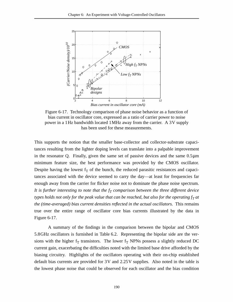
Chapter 6: An Experiment with Voltage-Controlled Oscillators
paci-
ment
.5
ator.
aci-
ies far
trum.
ce
f
ta in
OS
ver-
C
y the
ed
le is
dition
This supports the notion that the smaller base-collector and collector-substrate ca
tances resulting from the lighter doping levels can translate into a palpable improve
in the resonator Q. Finally, given the same set of passive devices and the same 0µm
minimum feature size, the best performance was provided by the CMOS oscill
Despite having the lowest fT of the bunch, the reduced parasitic resistances and cap
tances associated with the device seemed to carry the day—at least for frequenc
enough away from the carrier for flicker noise not to dominate the phase noise spec
It is further interesting to note that the fT comparison between the three different devi
types holds not only for the peak value that can be reached, but also for the operatingT at
the (time-averaged) bias current densities reflected in the actual oscillators.This remains
true over the entire range of oscillator core bias currents illustrated by the da
Figure 6-17.
A summary of the findings in the comparison between the bipolar and CM
5.8GHz oscillators is furnished in Table 6.2. Representing the bipolar side are the
sions with the higher fT transistors. The lower fT NPNs possess a slightly reduced D
current gain, exacerbating the difficulties noted with the limited base drive afforded b
biasing circuitry. Highlights of the oscillators operating with their on-chip establish
default bias currents are provided for 3V and 2.25V supplies. Also noted in the tab
the lowest phase noise that could be observed for each oscillator and the bias con
2 4 6 8 10 120
5
10
15
20
25
Figure 6-17. Technology comparison of phase noise behavior as a function ofbias current in oscillator core, expressed as a ratio of carrier power to noise
power in a 1Hz bandwidth located 1MHz away from the carrier. A 3V supplyhas been used for these measurements.
Bias current in oscillator core (mA)
(Ca
rrie
r/N
ois
e d
en
sity
)/1
010
Bipolardesigns
CMOS
High fT NPNs
Low fT NPNs
190

Chapter 6: An Experiment with Voltage-Controlled Oscillators
ited
w that
ise
plying
uits
g an
e.
from which it resulted. But here too, the bipolar versions were hindered by the lim
base drive, constraining the bias currents and the phase noise performance well belo
associated with the onset of the voltage-limited regime.
6.4 Observations on Oscillators
Resting on the foundation of a pair of oscillator topologies known for low no
performance and an ease of integration, a set of four VCOs has been designed by ap
insight gleaned from studying a linear time-variant model of oscillator behavior. Circ
were then developed to offer an adjustable bias feature in the oscillators, instillin
Table 6.2: Performance Summary for the C-band Monolithic VCOs
Bipolar CMOS
3V operation, “default” bias
Tuning range 5.4-6.1GHz0-3V
5.2-5.9GHz0-2V
Bias current in oscillator core 6.0mA 5.2mA
Biasing circuitry overhead 0.7mA 3.0mA
Phase noise, 100kHz offset -90dBc/Hz -83dBc/Hz
Phase noise, 1MHz offset -110dBc/Hz -112dBc/Hz
Reduced power: 2.25V, “default” bias
Bias current in oscillator core 4.6mA 2.8mA**
Phase noise, 1MHz offset -108dBc/Hz -105dBc/Hz**
Lowest noise operation (observed)
Supply voltage 3V* 5VBias current in oscillator core 11.9mA* 14mAPhase noise, 1MHz offset -113dBc/Hz* -121dBc/Hz
Output buffer (all modes)
Bias current @ 3V operation 4.4mA 4.7mA
Q of 6 for oscillator inductors (at 5.8GHz)*Performance is limited by saturation in the biasing circuitry.
** The “default” bias in the CMOS oscillator at 2.25V is in the voltage-limited regim
191

Chapter 6: An Experiment with Voltage-Controlled Oscillators
cern
r
airs.
ered
input
upon
tran-
reso-
elded
tran-
speed
sistor
r a
and
sting
eased
p-
and
celled
d a
an-
pli-
eater
cross-
y be
rrents
n the
added degree to controllability without degenerating the RF performance. Next, con
for providing isolation and the need to drive a 50Ω load for frequencies near the transisto
fT led to the design of two impedance-matched output buffers based on differential p
As with the biasing circuitry, much of the emphasis in the design of the buffers cent
around not degrading the performance of the oscillator, wherein a trade-off between
impedance and gain was noted to exist. Favoring the goal of minimizing the loading
the oscillator cores, the gain provided by the buffers wound up being rather modest.
Using the same suite of passive devices, oscillators were constructed of three
sistor types and optimized for the best performance each could attain. Although the
nator Q fell far short of the values predicted during the design, these three versions yi
some interesting comparisons. As an unmistakable exhibition of the role played by
sistor terminal parasitics, a ranking of the measured phase noise—in the f-2, white noise
dominated, region of the spectrum—went from best to worst as the device fT went from
lowest to highest. This is not to suggest an inverse relationship between switching
and oscillator noise, but does serve to indicate the relative unimportance of the tran
fT—once fT is beyond the oscillation frequency by a factor of 3 to 5. In the search fo
relevant figure of merit for transistors, fMAX fares no better as the same ordering (in fMAX )
occurs for the devices in this comparison.
In hindsight, the selection of the cross-coupled topology with both n-channel
p-channel pairs might not have been the best choice for the CMOS oscillator. By co
headroom through its stack of three devices, this architecture effectively trades incr
noise in the f-2 region for lower f-3 noise. And unless the match between n-channel and
channel drive strength is fairly precise, a difficult proposition to ensure over process
temperature, the degree to which the effects caused by low frequency noise are can
may not be particularly high. The best reported results have typically observe
reduction of 20-30dB in the upconversion of flicker noise, and it is not likely that any c
cellation technique would accomplish much more than this. While significant, for ap
cations where the noise at frequencies farther removed from the carrier is of gr
importance, better results probably would have been achieved had only one of the
coupled pairs been used.56
One other aspect of adaptive performance versus power consumption ma
worth considering. The reason that the phase noise improves with higher bias cu
(until voltage limitations set in) is that the amplitude of the signal increases faster tha
56 In addition, the noise in the f-3 region may even have been lower were only PMOS devices usedin the oscillator core.
192

Chapter 6: An Experiment with Voltage-Controlled Oscillators
rom
the
lator
l on
y the
and
eving
odels,
nduc-
ea-
hed a
rs for
match
ably
uctor
lable
sing
esigns
here
n dem-
ever,
gni-
e by
nsid-
latest
ng
noise. A mixer, provided that the oscillator is driving one, may also stand to benefit f
the higher signal level. A number of the more salient features of a mixer—including
noise figure, conversion gain, and linearity—generally improve with increased oscil
drive levels. Within the context of a receiver, this may constitute a two for one dea
sensitivity: as more power is spent in the oscillator, the signal to noise ratio supplied b
RF front end will be improved by lowering both reciprocal mixing due to phase noise
the noise figure of the mixer.
Once again, accurate inductor modeling is demonstrated to be central to achi
first-pass success in RFICs. Despite the repeated criticisms leveled at the scalable m
a few words are owed on their behalf: it should be noted that the beleaguered spiral i
tor models did not completely fail to find the mark. Although not shown among the m
surements in this chapter, the return loss at the output ports of the oscillators reac
very respectable 18dB, found centered at the targeted 5.8GHz. As the MIM capacito
the process run were very near the nominally specified values, the excellent output
indicates that the model for the inductor used in the oscillator buffers was reason
close. The one difference between this inductor and the others is that the buffer ind
was optimized for area rather than a high quality factor. Thus it appears that the sca
models provide better representations when the desired Qs are more modest.
So, after all of this, what is the best technology for oscillators? When posses
terminal resistances and capacitances on par with bipolar transistors, the CMOS d
have proven themselves to be very competitive in the arena of RF applications w
close-in phase noise tends to be less of a concern. Moreover, techniques have bee
onstrated to reduce both the effects and the occurrence of flicker noise [38][86]. How
when the device 1/f noise in vertical (silicon) bipolar transistors is three orders of ma
tude smaller than that exhibited by MOSFETs, a gap exists which is difficult to clos
circuit cancellation techniques. Given this advantage, and when properly scaled in co
eration of the lessons presented by this work, a bipolar technology making use of the
lithography tools will be difficult to beat. The primary challenge will be to avoid getti
caught up in an fT footrace.
193

Chapter 6: An Experiment with Voltage-Controlled Oscillators
194

ourse
has
time-
loped
by
xtent
w cir-
nsis-
m the
low-
by
rom
deter-
ed to
ng the
f mea-
.
upled
to be
a scal-
tion
wider
n
Chapter 7
Final Thoughts
Set against the backdrop of high data rate, adaptive wireless networks, a disc
into the concurrent optimization of circuits and technology for RF/microwave ICs
been presented. Approaches to considering the manifestation of noise in linear
invariant and linear time-variant RF circuits have been described, and were then deve
as tools for identifying the physical limitations to circuit performance as constrained
the devices. Design techniques were applied to mitigate these limitations to the e
possible while enabling the concept of adaptive performance, resulting in several ne
cuits, the illustration of a number of key effects, and the most direct comparison of tra
tor technologies conducted to date. Completing the story are measured results fro
characterization of an experimental set of voltage-controlled oscillators (VCOs) and
noise amplifiers (LNAs), offering confirmation for many of the observations reached
applying the tools fashioned herein.
This treatise began with a look at the modeling of on-chip spiral inductors. F
measurements at the circuit level and of an inductor test cell, it was subsequently
mined that an analytical treatment of the substrate (presented in Section 2.2) fail
accurately capture the loss mechanisms inherent to the medium. Instead, interpolati
substrate capacitance and resistance components for spiral inductors within a set o
sured data points would be a more effective avenue to realizing a scalable modelj1 In
addition, eddy currents in the substrate (Section 2.3) should be included through a co
secondary winding, and current crowding in the spiral trace (Section 2.2.1) needs
incorporated to represent behavior at gigahertz frequencies. Lacking these effects,
able model leads an optimization for quality factor astray by overpredicting the reduc
in the series resistance and underpredicting the substrate loss associated with using
metal traces.
j1 Full electromagnetic simulations tend to be too unwieldy for the optimization of an inductorgeometry; however, such simulations could be used to generate the data points for interpolatioby the scaling rules discussed in Section 2.2.
195

Chapter 7: Final Thoughts
and
for
was
pti-
d that
vable
ial-
noise
aci-
bout
istor f
gure
adi-
mitter
t, C
.4),
e the
ortant
essed
re of
ce
ele-
s then
sing
gure
, the
s of
ering
em-
t
One application where inductors prove instrumental is in tuning a narrowb
LNA stage for gain and low noise. A number of topologies were explored in Chapter 4
suitability as RF amplifiers; of those analyzed, the common-emitter configuration
found to work very well when equipped with base and emitter inductors to deliver o
mum noise and impedance matches to the RF source. Moreover, it was determine
the noise figure of this stage effectively represents the technological limit to the achie
sensitivity. This limit arrives at an optimum collector current density ( ); by mater
izing a balance between shot noise and gain, represents the current at which the
of a bipolar transistor is minimized, and it is solely a parameter of the technology.j2 In this
low noise regime, the operation of the device is primarily limited by the junction cap
tances. The minimum noise figure, and the power consumption required to bring a
this condition, both decrease as the junction capacitance is reduced; the peak transT
is actually of little consequence for an LNA. Given a fixed source resistance, noise fi
and power dissipation approximately follow , where the terms under the r
cal represent the base-emitter and base-collector junction capacitances per unit e
area (Section 4.2). Although often the smaller of the two by an appreciable amounµplays a significant role in many other features of an LNA including: stability (Section 4
isolation (Section 4.3), gain (Section 4.3.2), and noise figure (Section 4.1). Henc
depletion capacitances at both intrinsic device junctions should be considered imp
trade-offs at the device design level.
Having located the technology-imposed barriers, the next question to be addr
is the relation between the noise figure of an actual LNA and the minimum noise figu
a transistor. Starting with a 1.5dB NFmin in a 5.8GHz design, adding a cascode devi
resulted in a 0.3dB hit to the noise figure, and incorporating a reduced power mode
vated this figure another 0.25dB (Section 5.1). A base current source bias circuit wa
developed to protect linearity while keeping the noise figure degradation due to bia
well under 0.1dB (Section 5.1.3). The remaining notable contribution to the noise fi
occurs from loss in the inductors. When the quality factors are very good (17-19)
anticipated noise figure penalty is rather mild (0.2dB). However, with more typical Q
5-6, an increase of 1.2dB is attributable to the spiral inductors (Section 5.3). Consid
the constant transconductance biasing circuit, useful low power mode, and 50Ω imped-
ances required of a practical design for wireless applications, the LNA in this work d
onstrates that a 3.4dB (minimum) noise figure is achievablej3 in the 5-6GHz range using a
j2 The optimum current density does increase with the frequency of operation, but is independenof the device size.
j3 This is assuming an optimum noise match is provided for the LNA.
JCopt
JCopt
C′jE C′µ+
196

Chapter 7: Final Thoughts
above
her
NF
g the
ply,
in of
y the
g from
ncel.
rrent,
l (low
5.2),
ssoci-
ing
ained
er
oxi-
ere
ain
annel
r-
ifi-
riant
oise
ibit a
ns to
ting
e and
gener-
to
0.5µm SiGe graded-base bipolar process. This represents a cost of almost 2dB
NFmin for an individual transistor in the technology.
An interesting thought to ponder in light of a CMOS implementation is whet
the loss and added noise incurred due to the inductors might mask any disparities inmin
at the transistor level. This does not appear to be the case, however, in comparin
bipolar and CMOS LNAs discussed in Chapter 5. Dissipating 14mW from a 3V sup
the CMOS design delivered a minimum noise figure of 4.5dB and an available ga
5.2dB, falling short on both counts relative to the 3.4dB and 11dB numbers yielded b
bipolar LNA on only 8mW from the same 3V supply.j4 The 1.1dB disparity is roughly
the same as that expected between the intrinsic devices, a correspondence resultin
two differences in the impedance characteristics of the transistors which tend to ca
The input impedance presented by a MOSFET is relatively insensitive to the bias cu
making the adaptive performance concept possible without necessitating a paralle
power) stage. Unfortunately, power constraints limit the size of the FETs (Section
thus mandating more inductance to realize an input match; the higher inductor loss a
ated with the CMOS design offsets the benefit of not having to incur the penalty follow
from the parallel stage architecture. Another issue with MOSFET impedances pert
to whether an optimum source resistance of 50Ω could be achieved (for reasonable pow
dissipation levels). Although the expected from applying the long channel appr
mation is in the neighborhood of 90Ω, the measured optimum source impedances w
found outside the 50Ω circle; the correspondingly low values suggest that the dr
and induced gate noise currents are notably higher than predicted by the long ch
model—even in this 0.5µm technology.
While LNAs typify the design of LTI circuits for RF applications, another impo
tant class of circuits is exemplified by the periodic LTV behavior of oscillators. A sign
cant distinction between the two classes is that the sensitivity to noise in time-va
circuits is one of the parameters which may vary in time. As a corollary, the n
sources—particularly those associated with transistor conduction—may also exh
time-dependent power spectral density. In modeling this behavior, two key extensio
the work of Hajimiri and Lee [38] have been presented. The first extension is in no
that transistors in time-variant systems cannot be represented by equivalent voltag
current noise sources (Section 3.3). Each terminal resistance and conduction noise
j4 The available gain measurements represent the gain which could be achieved were the sourcepresent a reflection coefficientΓopt. However, the optimum source impedances determined forthe LNAs were not too far removed from 50Ω.
Rsopt
Rsopt
197
Chapter 7: Final Thoughts
lways
ond
ter-
3.4).
s are
lector-
noise.
n to
me
nol-
tion
cur-
f
ice;
e.
ed in
ator
hen
in
apaci-
as
se-
lector
rent
out-
cir-
often
veral
the
ator must be considered independently; thermal noise in terminal resistances is a
present while conduction noise may only exist during a fraction of the period. A sec
important addition to the LTV model is to recognize that conduction noise is not de
mined by the total current flowing into the corresponding transistor terminal (Section
In a bipolar transistor, significant portions of the base and collector terminal current
associated with charging and discharging the base-collector, base-emitter, and col
substrate depletion regions—capacitive components which do not generate shot
Failure to subtract the displacement currents in the calculation of noise was show
result in a significant error in a 5.8GHz design, illustrating an effect which will beco
increasingly profound at higher frequencies.
Resulting from this development is a tool by which the impact of a device tech
ogy can be considered for oscillators (and other LTV circuits). Discontinuous conduc
in oscillators—when timed appropriately—effectively de-emphasizes the transistor
rent noise sources. Once the transistor fT is a factor of 3 to 5 beyond the frequency o
oscillation, the time-varying behavior is controlled by the circuit and not the dev
beyond this point further increases in fT have no material effect on oscillator performanc
This assertion is demonstrated in a comparison of 5.8GHz oscillators present
Section 6.3: using the same inductors, a design implemented with 0.5µm CMOS transis-
tors (15GHz peak fT) produced lower phase noise in the f-2 region of the spectrum than
did the bipolar incarnations of the oscillator. Among the bipolar versions, the oscill
making use of lower fT NPNs (peaking at 27GHz) outperformed the same design w
NPNs with twice the (peak) fT were inserted. Of the three, CMOS emerged victorious
the comparison due to having smaller terminal access resistances and parasitic c
tances than the 0.5µm bipolar transistors in this technology. Similarly, lower noise w
obtained by the “slower” NPNs in the bipolar oscillator due to a reduction in the ba
collector and collector-substrate capacitances—achieved by masking an intrinsic col
implant designed to push out the onset of the Kirk effect (to higher collector cur
densities).j5
Although the RF signal paths have received most of the attention, biasing and
put loading can figure prominently in the circuit performance. Noise from the biasing
cuitry may easily overwhelm that in the signal path, necessitating careful design and
a non-negligible power consumption (in the bias circuits) to keep the noise low. Se
new circuit techniques were developed to mitigate this concern while extending
j5 “Slower” is chosen here primarily to reflect the general stigma attached with having a lowerpeak fT.
198

Chapter 7: Final Thoughts
sing
able
mpact
ting
), a
ing a
to
oise
O to
per-
.2.1).
esis-
h will
d for
f an
s
ireless
t role
s has
llector
being
r tech-
ffec-
n for
nium
le is
se
conti-
o
achievable RF performance through adjustability. A switched current source bia
approach was implemented for the bipolar LNA (Section 5.1.3), providing a st
transconductance (over temperature) and a high output impedance to minimize the i
on the noise figure and linearity of the amplifier. Although the topology and the insula
gate made the biasing chore much easier for the CMOS LNA (Section 5.2.3
temperature-stabilized transconductance was also realized within it by incorporat
∆VGSbias reference.j6 The circuit used for biasing the bipolar oscillators was designed
reuse reference legs to reduce power consumption while providing low n
(Section 6.1.3). Finally, a feedback biasing scheme was developed for the CMOS VC
allow control of the current in the oscillator core through a tail source device which o
ates in triode to maximize the voltage headroom afforded to the oscillation (Section 6
Each of these circuits provides a “default” bias condition established by an on-chip r
tor, but can be adjusted via an external input to support the adaptive operation whic
become a cornerstone of future, bandwidth on demand, wireless networks.
Through the designs presented in this work, an approach has been illustrate
thinking about the ramifications of a technology upon the LTI and LTV components o
RF system. From these examples in a 0.5µm BiCMOS process, a number of generalitie
have been extended to guide the development of semiconductor technologies for w
communications. One of the most poignant findings is that peak transistor fT is overem-
phasized for RF circuits. Simply put, a higher device fT does not automatically improve
everything; in fact, depending on which trade-offs are invoked, increasing the fT may actu-
ally translate to lower performance. Junction capacitances play a far more importan
in low noise, low power applications than does base transit time (τF), bringing into ques-
tion the trend toward thinner base devices. Accompanying the thinner base layer
been an increase in the doping concentrations applied to the (intrinsic) base and co
regions, leading to higher junction capacitances and hindering the RF performance
sought. The real improvements being observed from advanced silicon-based bipola
nologies can be traced to the continued shrinking in the lithographic dimensions, e
tively overcoming the penalties associated with recent directions in the stack desig
bipolar transistors. Another choice which should be questioned is the graded germa
profile incorporated into most modern SiGe bipolar technologies. A graded profi
adopted to reduceτF by creating a drift field for minority carriers in the base. But for u
in radio circuits, a box profile can provide advantages by creating a valence band dis
j6 Both LNAs will exhibit some residual temperature dependence as the on-chip resistors used testablish the current possess a non-zero TC. However, the first-order effects in the transconduc-tance have been compensated as illustrated through simulation in Figure 5-11.
199

Chapter 7: Final Thoughts
n of
titive
llator
-
will
and
tance.
e, as
tech-
haps
ent.
esses
lt to
nuity at the base-emitter junction. With an energy barrier in place to block the injectio
holes from the base, the emitter doping concentration can be lowered to reduce CjE.
For RF applications, CMOS has demonstrated performance that is compe
with implementations in mature bipolar processes—even winning along some osci
metrics. However, while the noise figure and fT in MOSFETs have seen marked improve
ments with scaling, the question going forward will be the extent to which this trend
continue in the face of high field mobility degradation and increases in the drain
induced gate noise currents which seem to be outpacing the gains in transconduc
Furthermore, the higher flicker noise in CMOS appears to remain a significant issu
low frequency noise can be addressed only to a degree through circuit cancellation
niques at RF—and not likely by enough to close the gap with bipolar devices. But per
the better question is to ask which device technology has more room for improvem
Keeping in mind the lessons advanced through this work, as CMOS and bipolar proc
are aggressively scaled, the performance of a bipolar technology will prove difficu
beat in the RF arena.
200

NII/
s
on
g
d in
Bibliography
Wireless Systems
[1] Federal Communications Commission News Report No. DC 96-36,CommissionProposes to Make Spectrum Available for Use by New Unlicensed Equipment; SUPERNet Devices Would Facilitate Interconnection to NII, April 25, 1996.
Inductor Modeling
[2] T. H. Lee,A Fully Integrated Inductorless FM Receiver, Sc.D. Thesis, MassachusettInstitute of Technology, December 1989.
[3] K. W. Kobayashi and A. K. Oki, “A Novel Heterojunction Bipolar Transistor VCOUsing an Active Tunable Inductance,”IEEE Microwave and Guided Wave Letters,July 1994, pp. 235-237.
[4] S. Hara and T. Tokumitsu, “Monolithic Microwave Active Inductors and TheirApplications,”IEEE International Sympoisum on Circuits and Systems, June 1991,pp. 1857-1860.
[5] P. R. Nuytkens, et al., “A Monolithic Tunable High-Q InAlAs/n+–InP–HFETResonator,”Indium Phosphide and Related Materials Conference, April 1993,pp. 389-392.
[6] C. H. Leong and G. W. Roberts, “A Sixth-Order UHF Bandpass Filter using SilicBipolar Active Inductors,”International Symposium on Circuits and Systems,June 1998, pp. 127-130.
[7] D. A. Hitko, A Low Power, Low Noise, 1.8GHz Voltage-Controlled Oscillator, S.M.Thesis, Massachusetts Institute of Technology, February 1997, chapter 3.
[8] M. Steyaert and J. Craninckx, “1.1GHz Oscillator Using Bondwire Inductance,”IEEElectronics Letters, February 3, 1994, pp. 244-245.
[9] T. I. Ahrens and T. H. Lee, “A 1.4-GHz 3-mW CMOS LC Low Phase Noise VCOUsing Tapped Bond Wire Inductances,”International Symposium on Low PowerElectronics and Design, August 1998, pp. 16-19.
[10] P. J. Sullivan, et al., “An Integrated CMOS Distributed Amplifier Utilizing PackaginInductance,”IEEE Transactions on Microwave Theory and Techniques,October 1997, pp. 1969-1976.
[11] D. C. Laney, et al., “Lateral Microwave Transformers and Inductors Implementea Si/SiGe HBT Process,”IEEE MTT-S International Microwave Symposium,June 1999, pp. 855-858.
201

Bibliography
f
iO
,”
s,”
elds
.
[12] J. R. Long and M. A. Copeland, “The Modeling, Characterization, and Design oMonolithic Inductors for Silicon RF IC’s,”IEEE Journal of Solid-State Circuits,March 1997, pp. 357-369.
[13] F. W. Grover,Inductance Calculations: Working Formulas and Tables, D. VanNostrand Company, New York, 1946.
[14] H. Hasegawa, M. Furukawa, and H. Yanai, “Properties of Microstriplines on Si-S2System,”IEEE Transactions on Microwave Theory and Techniques, November 1971,pp. 869-881.
[15] E. Pettenpaul, et al., “CAD Models of Lumped Elements on GaAs up to 18GHzIEEE Transactions on Microwave Theory and Techniques, February 1988,pp. 294-304.
[16] C. P. Yue and S. S. Wong, “Physical Modeling of Spiral Inductors on Silicon,”IEEETransactions on Electron Devices, March 2000, pp.560-568.
[17] A. M. Niknejad and R. G. Meyer, “Analysis, Design, and Optimization of SpiralInductors and Transformers for Si RF IC’s,”IEEE Journal of Solid-State Circuits,October 1998, pp. 1470-1481.
[18] H. M. Greenhouse, “Design of Planar Rectangular Microelectronic Inductors,”IEEETransactions on Parts, Hybrids, and Packages, June 1974, pp. 101-109.
[19] S. S. Mohan, et al., “Simple Accurate Expressions for Planar Spiral InductanceIEEE Journal of Solid-State Circuits, October 1999, pp. 1419-1424.
[20] W. B. Kuhn and N. M. Ibrahim, “Approximate Analytical Model of CurrentCrowding Effects in Multi-Turn Spiral Inductors,”IEEE Radio Frequency IntegratedCircuits Symposium, June 2000, pp. 271-274.
[21] C. P. Yue and S. S. Wong, “On-chip Spiral Inductors with Patterned Ground Shifor Si-based RF IC’s,”IEEE Journal of Solid-State Circuits, May 1998, pp. 743-752.
[22] H. G. Booker,Energy in Electromagnetism, Peter Peregrinus Ltd., New York, 1982[23] C. A. Desoer and E. S. Kuh,Basic Circuit Theory, McGraw-Hill, Inc., New York,
1969; refer to the applications of Tellegen’s Theorem in Chapter 9, Section 5.4.[24] K. O, “Estimation Methods for Quality Factors of Inductors Fabricated in Silicon
Integrated Circuit Process Technologies,”IEEE Journal of Solid-State Circuits,August 1998, pp. 1249-1252.
[25] MATLAB, Mathworks, Inc.,http://www.mathworks.com, Natick, MA.[26] FastHenry, Research Laboratory of Electronics, Massachusetts Institute of
Technology,ftp://rle-vlsi.mit.edu/pub/fasthenry, Cambridge, MA.
Oscillator and Mixer Modeling
[27] K. Kurokawa, “Some Basic Characteristics of Broadband Negative ResistanceOscillator Circuits,”Bell System Technical Journal, July-August 1969, pp. 1937-1955.
[28] D. B. Leeson, “A Simple Model of Feedback Oscillator Noise Spectrum,”Proceedings of the IEEE, February 1966, pp. 329-330.
[29] H. K. Lindenmeier, “Noise Matching Techniques in Transistor Oscillators,”IEEECircuits and Systems Symposium, 1980, pp. 1052-1055.
202

Bibliography
.
n
[30] T. H. Lee,The Design of CMOS Radio-Frequency Integrated Circuits, CambridgeUniversity Press, New York, 1998, chapter 12.
[31] J. Groszkowski, “The Interdependence of Frequency Variation and HarmonicContent, and the Problem of Constant-Frequency Oscillators,”Proceedings of theIRE, vol. 21, no. 7, 1934, pp. 958-981.
[32] Private communication with Dan McMahill.[33] G. R. Olbrich, et al., “Calculation of HEMT Oscillator Phase Noise Using Large
Signal Analysis in Time Domain,”IEEE MTT-S International MicrowaveSymposium, June 1994, pp. 965-968.
[34] A. Hajimiri and T. H. Lee,The Design of Low Noise Oscillators, Kluwer AcademicPublishers, Norwell, MA, 1999, Chapter 4.
[35] C. D. Hull and R. G. Meyer, “A Systematic Approach to the Analysis of Noise inMixers,” IEEE Transactions on Circuits and Systems I, December 1993, pp. 909-919
[36] F. X. Kärtner, “Analysis of White and f-α Noise in Oscillators,”International Journalof Circuit Theory and Applications, September-October 1990, pp. 485-519.
[37] A. Hajimiri and T. H. Lee,The Design of Low Noise Oscillators, Kluwer AcademicPublishers, Norwell, MA, 1999, Appendix B.
[38] A. Hajimiri and T. H. Lee, “A General Theory of Phase Noise in ElectricalOscillators,”IEEE Journal of Solid-State Circuits, February 1998, pp. 179-194.
[39] A. Demir, A. Mehrotra, and J. Roychowdhury, “Phase Noise in Oscillators: AUnifying Theory and Numerical Methods for Characterization,”IEEE Transactionson Circuits and Systems I, May 2000, pp. 655-674.
[40] J. Rael and A. Abidi, “Physical Processes of Phase Noise in Differential LCOscillators,”IEEE Custom Integrated Circuits Conference, May 2000, pp. 569-572.
[41] Q. Huang, “Phase Noise to Carrier Ratio in LC Oscillators,”IEEE Transactions onCircuits and Systems I, July 2000, pp. 965-980.
[42] J. Philips and K. Kundert, “Noise in Mixers, Oscillators, Samplers, and Logic: AIntroduction to Cyclostationary Noise,”IEEE Custom Integrated CircuitsConference, May 2000, pp. 431-438.
[43] Y. Taur and T. H. Ning,Fundamentals of Modern VLSI Devices, CambridgeUniversity Press, New York, 1998, chapter 7.
[44] T. H. Lee,The Design of CMOS Radio-Frequency Integrated Circuits, CambridgeUniversity Press, New York, 1998, chapter 4.
Low-Noise Amplifiers
[45] E. Taniguchi, et al., “Dual Bias Feed SiGe HBT Low Noise Linear Amplifier,”IEEEInternational Microwave Symposium (MTT-S), 2001, pp. 285-288.
[46] D. Yongwang and R. Harjani, “A +18 dBm IIP3 LNA in 0.35µm CMOS,” IEEEInternational Solid-State Circuits Conference, 2001, pp. 162-163.
[47] G. D. Vendelin, A. M. Pavio, and U. L. Rohde,Microwave Circuit Design UsingLinear and Nonlinear Techniques, John Wiley & Sons, New York, 1990, chapter 4.
[48] A. van der Ziel, Noise:Sources, Characterization, and Measurement, Prentice Hall,Englewood Cliffs, NJ, 1970, chapter 7.
203

Bibliography
r
,
e
[49] S. P. Voinigescu, et al., “A Scalable High-Frequency Noise Model for BipolarTransistors with Application to Optimal Transistor Sizing for Low-Noise AmplifieDesign,”IEEE Journal of Solid-State Circuits, September 1997, pp. 1430-1439.
[50] M. Schröter and H.-M. Rein, “Transit Time of High-Speed Bipolar Transistors inDependence on Operating Point, Technological Parameters, and Temperature,”IEEEBipolar Circuits and Technology Meeting, 1989, pp. 250-253.
[51] P. R. Gray, et al.,Analysis and Design of Analog Integrated Circuits, 4th edition,John Wiley & Sons, New York, 2001, chapter 11.
[52] E. G. Nielsen, “Behavior of Noise Figure in Junction Transistors,”Proceedings of theIRE, July 1957, pp. 957-963.
[53] D. K. Lynn, C. S. Meyer, and D. J. Hamilton, editors,Analysis and Design ofIntegrated Circuits, McGraw-Hill, New York, 1967, chapter 12.
[54] Carl Battjes, Tektronix Inc., Beaverton, OR,Monolithic Wideband Amplifier, U.S.Patent 4,236,119, November 25, 1980.
[55] D. L. Feucht,Handbook of Analog Circuit Design, Academic Press, San Diego, CA1990, chapter 10.
[56] C. T. Armijo and R. G. Meyer, “A New Wide-Band Darlington Amplifier,”IEEEJournal of Solid-State Circuits, August 1989, pp. 1105-1109.
[57] S. Krishnan, et al., “Broadband Lumped HBT Amplifiers,”Electronics Letters,March 2000, pp. 466-467.
[58] J. S. Yuan,SiGe, GaAs, and InP Heterojunction Bipolar Transistors, Wiley & Sons,New York, 1999, chapter 2.
[59] A. Schmidt and S. Catala, “A Universal Dual Band LNA Implementation in SiGeTechnology for Wireless Applications,”IEEE Journal of Solid-State Circuits, July2001, pp. 1127-1131.
[60] R. S. Carson,High-Frequency Amplifiers, Second Edition, Wiley & Sons, New York,1982, chapter 7.
[61] Y. Tsividis,Operation and Modeling of the MOS Transistor, Second Edition,McGraw-Hill, Boston, MA, 1999, chapter 8.
[62] B. Sklar,Digital Communications, Second Edition, Prentice Hall, Upper SaddleRiver, NJ, 2001, chapter 4.
[63] T. H. Lee,The Design of CMOS Radio-Frequency Integrated Circuits, CambridgeUniversity Press, New York, 1998, chapter 4.
[64] J. Colvin, S. Bhatia, and K. O, “A Bond-Pad Structure for Reducing Effects ofSubstrate Resistance on LNA Performance in a Silicon Bipolar Technology,”BipolarCircuits and Technology Meeting, 1998, pp. 109-112.
[65] C. Biber, et al., “Technology Independent Degradation of Minimum Noise FigurDue to Pad Parasitics,”IEEE Microwave Theory and Techniques Symposium, 1998,pp. 145-148.
[66] R. Fried, Y. Blecher, and S. Friedman, “CMOS ESD Protection Structures—Characteristics and Performance Comparison,”Physical and Failure Analysis ofIntegrated Circuits Symposium, 1995, pp. 106-109.
[67] Y. Taur and T. H. Ning,Fundamentals of Modern VLSI Devices, CambridgeUniversity Press, New York, 1998, chapter 5.
204

Bibliography
the
rs02.
ies
C
,”
[68] B. Razavi, R.-H. Yan, and K. F. Lee, “Impact of Distributed Gate Resistance onPerformance of MOS Devices,”IEEE Transactions on Circuits and Systems I,November 1994, pp. 750-754.
[69] A. van der Ziel, “Thermal Noise in Field-Effect Transistors,Proceedings of the IRE,August 1962, pp. 1808-1812.
[70] A. van der Ziel, “Gate Noise in Field Effect Transistors at Moderately HighFrequencies,”Proceedings of the IEEE, March 1963, pp. 461-467.
[71] D. K. Shaeffer and T. H. Lee, “A 1.5-V, 1.5-GHz CMOS Low Noise Amplifier,”IEEE Journal of Solid-State Circuits, May 1997, pp. 745-759.
[72] N. Sano, et al., “Physical Mechanism of Current Fluctutation under Ultra-SmallDevice Structures,”IEEE International Workshop on Computational Electronics,1998, pp. 112-115.
[73] Y. C. Yeo, et al., “Direct Tunneling Gate Leakage Current in Transistors withUltrathin Silicon Nitride Gate Dielectric,”IEEE Electron Device Letters, November2000, pp. 540-542.
[74] T. C. Sepke,Investigation of Noise Sources in Scaled CMOS Field-Effect Transisto,S.M. Thesis, Massachusetts Institute of Technology, to be published in June 20
[75] A. van der Ziel, Noise:Sources, Characterization, and Measurement, Prentice Hall,Englewood Cliffs, NJ, 1970, chapter 6.
[76] D. K. Shaeffer and T. H. Lee,Low-Power CMOS Radio Receivers, Kluwer AcademicPublishers, Norwell, MA, 1999, chapter 4.
[77] T. H. Lee,The Design of CMOS Radio-Frequency Integrated Circuits, CambridgeUniversity Press, New York, 1998, chapter 11.
[78] C. Enz, “An MOS Transistor Model for RF IC Design Valid in All Regions ofOperation,”IEEE Transactions on Microwave Theory and Techniques, January 2002,pp. 342-359.
[79] S.-D. Kim, C.-M. Park, and J. C. S. Woo, “Advanced Model and Analysis of SerResistance for CMOS Scaling Into Nanometer Regime,”IEEE Transactions onElectron Devices, March 2002, pp. 457-472.
Oscillator Design
[80] D. A. Hitko, A Low Power, Low Noise, 1.8GHz Voltage-Controlled Oscillator, S.M.Thesis, Massachusetts Institute of Technology, February 1997, chapter 2.
[81] D. A. Hitko, A Low Power, Low Noise, 1.8GHz Voltage-Controlled Oscillator, S.M.Thesis, Massachusetts Institute of Technology, February 1997, chapter 4.
[82] D. Ham and A. Hajimiri, “Concepts and Methods in Optimization of Integrated LVCOs,” IEEE Journal of Solid-State Circuits, June 2001, pp. 896-909.
[83] T. H. Lee,The Design of CMOS Radio-Frequency Integrated Circuits, CambridgeUniversity Press, New York, 1998, chapter 17.
[84] E. Hegazi, et al., “A Filtering Technique to Lower Oscillator Phase Noise,”IEEEInternational Solid-State Circuits Conference, 2001, pp. 364-365.
[85] K. Gulati and H-S. Lee, “A High-Swing CMOS Telescopic Operational AmplifierIEEE Journal of Solid-State Circuits, December 1998, pp. 2010-2019.
205

Bibliography
on
[86] E. A. M. Klumperink, et al., “Reducing MOSFET 1/f Noise and Power Consumptiby Switched Biasing,”IEEE Journal of Solid-State Circuits, July 2000,pp. 994-1001.206