circuit analysis ii - university of oxford · circuit analysis ii (ac circuits) syllabus complex...
TRANSCRIPT

Will Moore
MT 12
CIRCUIT ANALYSIS II
(AC Circuits)
Syllabus
Complex impedance, power factor, frequency response of AC networks
including Bode diagrams, second-order and resonant circuits, damping
and Q factors. Laplace transform methods for transient circuit analysis
with zero initial conditions. Impulse and step responses of second-order
networks and resonant circuits. Phasors, mutual inductance and ideal
transformers.
Learning Outcomes
At the end of this course students should:
1. Appreciate the significance and utility of Kirchhoff’s laws.
2. Be familiar with current/voltage relationships for resistors, capacitors
and inductors.
3. Appreciate the significance of phasor methods in the analysis of AC
circuits.
4. Be familiar with use of phasors in node-voltage and loop analysis of
circuits.
5. Be familiar with the use of phasors in deriving Thévenin and Norton
equivalent circuits
6. Be familiar with power dissipation and energy storage in circuit
elements.

2
7. Be familiar with methods of describing the frequency response of
AC circuits and in particular
8. Be familiar with the Argand diagram and Bode diagram methods
9. Be familiar with resonance phenomena in electrical circuits
10. Appreciate the significance of the Q factor and damping factor.
11. Appreciate the significance of the Q factor in terms of energy
storage and energy dissipation.
12. Appreciate the significance of magnetic coupling and mutual
inductance.
13. Appreciate the transformer as a means to transform voltage, current
and impedance.
14. Appreciate the importance of transient response of electrical
circuits.
15. Be familiar with first order systems
16. Be familiar with the use of Laplace transforms in the analysis of the
transient response of electrical networks.
17. Appreciate the similarity between the use of Laplace transform and
phasor techniques in circuit analysis.

Circuit Analysis II WRM MT12
3
AC Circuits
1. Basic Ideas
Our development of the principles of circuit analysis in Circuit Analysis I
was in terms of DC circuits in which the currents and voltages were
constant and so did not vary with time. Here in Circuit Analysis II we
extend our analysis to consider time varying currents and voltages and
thereby we are able to extend our analysis to include capacitors and
inductors. In our initial discussions we will limit ourselves to sinusoidal
functions. We choose this special case because, as you have now
learnt in P1, it allows us to make use of some very powerful and helpful
mathematical techniques. It is also a common waveform in nature and it
is easy to generate in the lab. However as you have also learnt in P1,
any waveform can be expressed as a weighted superposition of
sinusoids of different frequencies and hence if we analyse a linear circuit
for sinusoidal functions we can, by appropriate superposition, handle
any function of time.
Let's begin by considering a sinusoidal variation in voltage
tVv m cos

4
in which is the angular frequency and is measured in radians/second.
Since the angle t must change by 2 radians in the course of one
period, T, it follows that
2T
However the time period f
T1
where f is the frequency measured in
Hertz. Thus
fT
22
This is a simple and very important relationship. We naturally measure
frequency in Hz – the mains frequency in the UK is 50Hz – and it is easy
to measure the time period, fT 1 from an oscilloscope screen.
However as we will soon see, it is mathematically more convenient to
work in terms of the angular frequency . Mistakes may be easily made
because in practice the word frequency is commonly used to refer to

Circuit Analysis II WRM MT12
5
both and f. It is important in calculations to make sure that if
appears, then the correct value for f = 50 Hz, say, is = 100 rads/sec.
A simple point to labour I admit, but if I had a pound for every time
someone forgets and substitutes = 50 . . . . . . . . !!
In our example above, tVv m cos , it was convenient that
0 tVv m at . In general this will not be the case and the waveform will
have an arbitrary relationship to the origin t = 0 or, equivalently the origin
may have been chosen arbitrarily and the voltage, say, may be written in
terms of a phase angle, , as
tVv m cos
Alternatively, in terms of a different phase angle, , the same waveform
can be written
T

6
tVv m sin
where
2
The phase difference between two sinusoids is almost always measured
in angle rather than time and of course one cycle (i.e. one period)
corresponds to 2 or 360. Thus we might say that the waveform above
is out of phase with the earlier sinusoid by . When 2 we say
that the two sinusoids are said to be in quadrature. When the
sinusoids are in opposite phase or in antiphase.
2. RMS Values
We refer to the maximum value of the sinusoid, Vm, as the “peak” value.
On the other hand, if we are looking at the waveform on an oscilloscope,
it is usually easier to measure the “peak-to-peak” value 2Vm, i.e. from the
bottom to the top. However, you will notice that most meters are
calibrated to measure the root-mean-square or rms value. This is found,
as the name suggests, for a particular function, f, by squaring the
function, averaging over a period and taking the (positive) square root of
the average. Thus the rms value of any function f(x), over the interval x
to x+X, where X denotes the period is

Circuit Analysis II WRM MT12
7
dyyfX
fXx
xrms
21
For our sinusoidal function tVv m cos
The average of the square is given by
dttVT
m
T
22
0
cos1
where the time period 2T . At this point it's probably easiest to
change variables to t and to write 2cos12
1cos2 . Thus the
mean square value becomes
2
2cos122
1 22
0
2mm V
dV
The root mean square value, which is simply the positive square root of
this, may be written as
Vrms = Vm /√2 ≈ 0.7 Vm.

8
Since we nearly always use rms values in our AC analysis, we assume
rms quantities unless told otherwise so by convention we just call it V as
in:
V = Vm /√2.
So, for example, when we say that the UK mains voltage is 230V what
we are really saying is that the rms value 230V. Its peak or maximum
value is actually 230√2 ≈ 325 V.
To see the real importance of the rms value let's calculate the power
dissipated in a resistor.
Here the current is given by Rvi
tItR
Vi m
m coscos

Circuit Analysis II WRM MT12
9
where RVI mm and the power, vip , is given by
tR
Vp m 2
2
cos
If we want to calculate the average power dissipated over a cycle we
must integrate from 20 Ttt to . If we again introduce t ,
the average power dissipated, P, is given by
dR
VP m 2
2
0
2
cos.2
1
dR
VP m 2cos1
2
1.
2
1 2
0
2
RVP m 22
If we now introduce the rms value of the voltage 2mVV then the
average power dissipated may be written as
RVP 2
Indeed if the rms value of the current 2mII is also introduced then
RIRVP 22

10
which is exactly the same form of expression we derived for the DC
case.
Therefore if we use rms values we can use the same formula for the
average power dissipation irrespective of whether the signals are AC or
DC.
3. Circuit analysis with sinusoids
Let us begin by considering the following circuit and try to find an
expression for the current, i, after the switch is closed.

Circuit Analysis II WRM MT12
11
The Kirchhoff voltage law permits us to write
tVRidt
diL m cos
This is a linear differential equation, which you know how to solve.
We begin by finding the complementary function, from the homogeneous
equation:
0Ridt
diL
which yields the solution:
LRtAi exp
We now need to find the particular integral which, for the sinusoidal
"forcing function" tVm cos , will take the form tCtB sincos . Thus
the full solution is given by
tCtBLRtAti sincosexp

12
We see that the current consists of a "transient" term, LRtA exp ,
which eventually decays and becomes negligible in comparison with the
"steady state" response. The transient response arises because of the
sudden opening or closing of a switch but we will concentrate here on
the final sinusoidal steady state response. How long do we have to wait
for the steady state? If for example 100R and mHL 25 then
13 sec104 LR and so after only 1ms 018.04expexp LRt
and so any measurements we are likely to make on this circuit will be
truly 'steady state' measurements. Thus our solution of interest reduces
to
tCtBi sincos
In order to find B and C we need to substitute this expression back into
the governing differential equation to give
tVtCtBRtBtCL m cossincossincos

Circuit Analysis II WRM MT12
13
It is now a simple matter to compare coefficients of cost and sint to
obtain expressions for B and C which lead, after a little algebra, to
tLtR
LR
Vi m
sincos
22
If we now introduce the inductive reactance LXL we can write this
equation as
t
XR
Xt
XR
R
XR
Vi
L
L
LL
m sincos222222
The expression in curly brackets is of the form
ttt cossinsincoscos
and hence
i =Vm
R 2 +XL
2cos wt -j( )
where
j = tan-1 X L
R
æ
èç
ö
ø÷
Thus we see that the effect of the inductor has been to introduce a
phase lag between the current flowing in the circuit and the voltage
source. Similarly the ratio of the maximum voltage to the maximum

14
current is given by 22LXR which since it is a combination of
resistance and reactance is given the new name of impedance.
It is apparent that we could solve all networks containing combinations
of resistors, inductors and capacitors in this way. We would end up with
a series of simultaneous equations to solve – just as we did when
analysing DC circuits – the problem is that they would be simultaneous
differential equations which, given the effort we went through to solve
one equation in the simple example above, would be very tedious and
therefore rather error-prone. Fortunately there is an easier way.
We are saved because the differential equations we have to solve are
linear and hence the principle of superposition applies. This tells us
that if a forcing function v1(t) produces current i1(t) and a forcing function
tv2 provides current ti2 then tvtv 21 produces titi 21 . The
trick then is to choose a more general forcing function tvtvtv 21 in
which, say, tv1 corresponds to tVm cos and which made the
differential equation easy to solve. We achieve this with complex
algebra.
You should know that
exp j wt =coswt + j sinwt.
where j = (-1), [electrical engineers like to use i for current]
so let’s solve the differential equation with the general forcing function

Circuit Analysis II WRM MT12
15
v t( )=Vm
exp j wt =Vm
coswt + j Vm
sinwt
where
v1t( )=Re v t( ){ }=Re V
mexp j wt{ }=V
mcoswt
.
The solution will be of the form
i (t ) =I exp jwt
where will, in general, be a complex number. Then in
order to find that part of the full solution corresponding to the real part of
the forcing function, tjVm exp we merely need to find the real part of
ti . Thus
i1t( )=Re I exp jwt{ }=Re I exp j wt -j( ){ }
= I cos wt -j( )
Let's illustrate this by returning to our previous example where we tried
to solve:
tVRidt
diL m cos
Now, instead, we solve the more general case:
tjVRidt
diL m exp

16
and take the real part of the solution. As suggested above an
appropriate particular integral is tjIi exp which leads to
tjVtjRItjILj m expexpexp
The factor tj exp is common and hence
mVILjR
in which LjR may be regarded as a complex impedance. The
complex current I is now given by
j
LR
V
LjR
VI mm exp
22
with RL 1tan and hence
tLR
VtjIti m cosexpRe
22
which, thankfully, is the same solution as before but arrived at with
considerably greater ease.
Let us be clear about the approach. We have

Circuit Analysis II WRM MT12
17
(i) introduced a complex forcing function tjVm exp knowing that in
reality the voltage source must be real i.e. tjVm expRe .
(ii) We solved the equations working with complex voltages and
complex currents, tjV exp and tjI exp (or rather V and I since the
time dependence exp jt cancelled out).
(iii) Since the actual voltage is given by tjVm expRe the actual
current is given by tItjjItjI cosexpexpReexpRe .
(iv) Since the differential of is simply
and since we always take out as a
common factor, you may see now that our differential equations turn into
polynomial equations in jω (and you knew how to solve these at GCSE!)
This is a very powerful approach that will permit us to solve AC circuit
problems very easily.

18
4. AC Circuit theory -- Example
Let's now do an example to show, formally, how we can solve AC
problems. Let's imagine we want to find the steady state current, i2,
flowing through the capacitor in the following example
The two KVL loop equations may be written
Ri1+Ldi
1
dt+R i
1- i
2( )=Em
cos wt +a( )
and
R i2- i
1( )+1
Ci
2dt =0ò

Circuit Analysis II WRM MT12
19
Replacing ( ) +cos tEm by ( ) tjEtjEm exp=+exp 1 where
jEE m exp=1 and further introducing I1 and I2 via
tjIitjIi exp=exp= 2211 and we obtain
01
2
12
121
IRICj
R
EIRILjR
and, after a little algebra
NjM
jE
CLj
CR
LR
EI m
exp
2
12
where CRLRM and CLN 2 . We note that this may be
written, introducing MNtan
jNM
EI m exp
222
and hence the actual current tjIi expRe 22 may be written as
tNM
Eti m cos
222
20
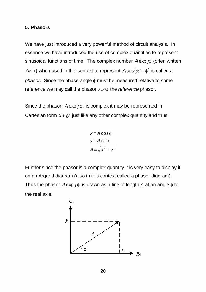
5. Phasors
We have just introduced a very powerful method of circuit analysis. In
essence we have introduced the use of complex quantities to represent
sinusoidal functions of time. The complex number jAexp (often written
A ) when used in this context to represent tAcos is called a
phasor. Since the phase angle must be measured relative to some
reference we may call the phasor 0A the reference phasor.
Since the phasor, jAexp , is complex it may be represented in
Cartesian form jyx just like any other complex quantity and thus
22 +=
sin=
cos=
yxA
Ay
Ax
Further since the phasor is a complex quantity it is very easy to display it
on an Argand diagram (also in this context called a phasor diagram).
Thus the phasor jAexp is drawn as a line of length A at an angle to
the real axis.
Circuit Analysis II WRM MT12
21
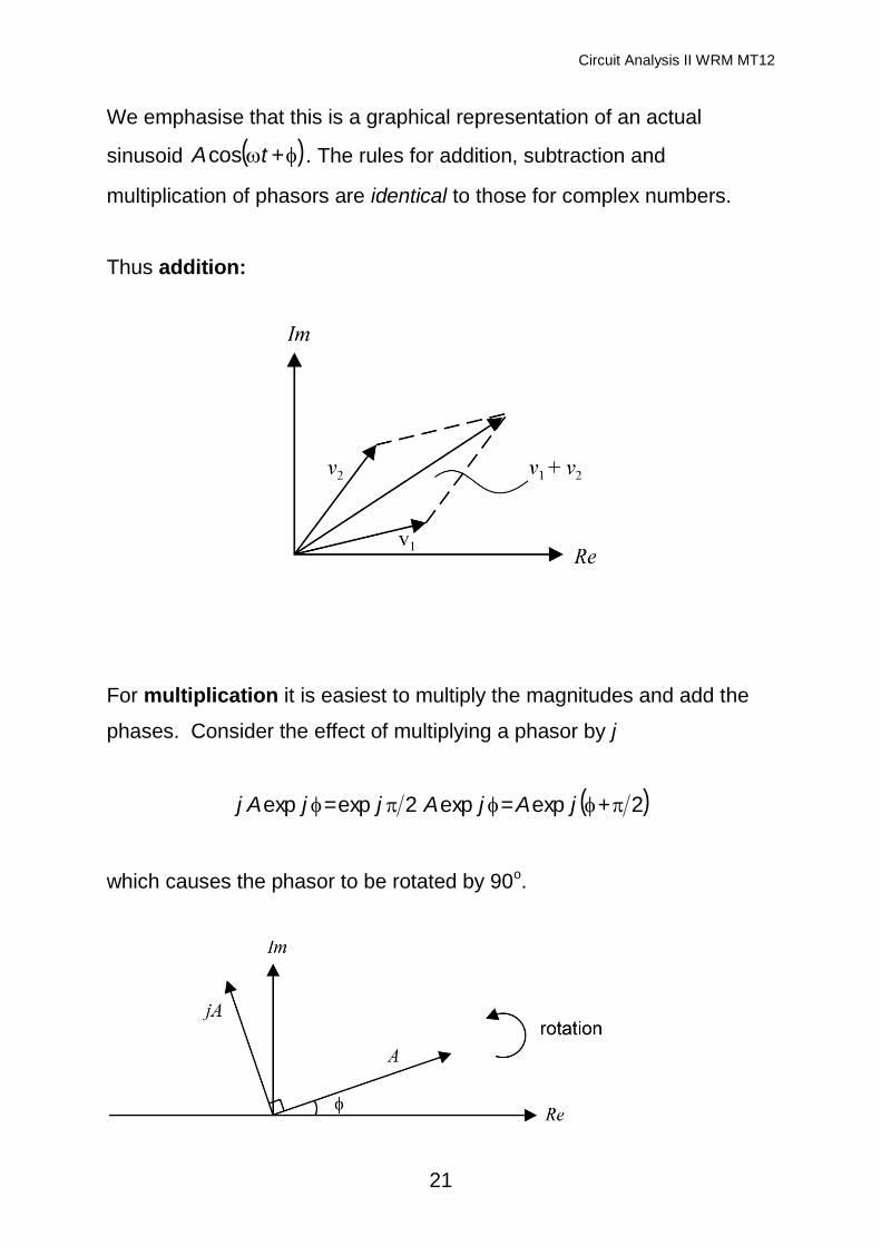
We emphasise that this is a graphical representation of an actual
sinusoid ( ) +cos tA . The rules for addition, subtraction and
multiplication of phasors are identical to those for complex numbers.
Thus addition:
For multiplication it is easiest to multiply the magnitudes and add the
phases. Consider the effect of multiplying a phasor by j
( )2+exp=exp2exp=exp jAjAjjAj
which causes the phasor to be rotated by 90o.

22
Similarly, dividing by j leads to
2expexp2expexp1
jAjAjjAj
i.e. a rotation of –90o.
We finally note that it is usual to use rms values for the magnitude of
phasors.

Circuit Analysis II WRM MT12
23
6. Phasor relations in passive elements
Consider now a voltage tVm cos applied to a capacitor. As we have
indicated we elect to use the complex form tjVm exp and so omit the
"real part" as we calculate the current via
( ) tjVCjtjVdt
dC
dt
dvCi mm exp=exp==
If we now drop the tj exp notation and write the voltage phasor Vm as
V and the current phasor as I we have
VCjI = or ICj
V
1=
In terms of a phasor diagram, taking the voltage V as the reference
from which we confirm two things we already knew

24
(i) the ratio of the voltage to the current is C
1
- the reactance.
(ii) the current leads the voltage by 90. The pre-multiplying factor j
describes this.
For the inductance an analogous procedure leads to
ILjV =
Where the reactance is now jωL and, if we now take, say, the current as
the reference phasor we have
and here the current lags the voltage by 90.

Circuit Analysis II WRM MT12
25
[It is important to get these relationships the right way around and as a
check we may use the memory aid “CIVIL” – in a capacitor, the current
leads the voltage CIVIL and in an inductor, the current lags the voltage
CIVIL.]
Finally for a resistor we know that the current and voltage are in phase
and hence, in phasor terms
RIV =

26
7. Phasors in circuit analysis
We are now in a position to summarise the method of analysis of AC
circuits.
(i) We include all reactances as imaginary quantities ( )LXjLj = for
an inductor and cXjCj 1 for a capacitor.
(ii) All voltages and currents are represented by phasors, which usually
have rms magnitude, and one is chosen as a reference with zero phase
angle.
(iii) All calculations are carried out in complex notation.
(iv) The magnitude and phase of, say, the current is obtained as
jI exp . This can, if necessary, be converted back into a time varying
expression ( ) +cos2 tI .

Circuit Analysis II WRM MT12
27
Suppose we wish to find the current flowing through the inductor in the
circuit below
The reactances have been calculated and marked on the diagram. The
left hand voltage source has been chosen as reference and provides
10V rms. The right hand source produces 5V rms but at a phase angle
of 37 with respect to the 10V source. If we introduce phasor loop
currents I1 and I2 as shown then we may write KVL loop equations as
212
211
5103437exp5
10510
IjjIIjj
IIjI
o
where we have noted that 3+4=37sin5+37cos5=37exp5 jjj ooo. It
is routine to solve these simultaneous equations to give
5.12
71
jI
and
5.12
8+5.6=2
jI
and hence the current 21 III becomes
-

28
oo jj
I 8.86exp72.08.8672.05.12
95.0
Since rms values are involved, if we want to convert this into a function
of time we must multiply by 2 to obtain the peak value. Thus
otti 8.86cos02.1
In our example we do not know the value of but it was accounted for in
the value of the reactances. Since everything is linear and the sources
are independent it would be a good exercise for you to check this result
by using the principle of superposition.
We have used mesh or loop analysis in our examples so far. It is, of
course equally appropriate to use node-voltage analysis if that looks like
an easier way to solve the problem.
As an example let's suppose we would like to find the voltage V in the
circuit below where the reactances have been calculated corresponding
to the frequency, , of the source

Circuit Analysis II WRM MT12
29
It's probably as easy as anything to introduce two phasor node voltages
V1 and V. The two node voltage relationships may be written as
05
0
510
10 111
j
V
j
VVV
and
0105
0
105
0
51
j
V
j
V
j
VV
We note that in writing these equations no thought was given to whether
currents flowing into or out of the nodes were being considered. As in
the DC case it is merely necessary to be consistent. It is now
straightforward to solve these two simultaneous equations to yield
oV 6.71101 or, if the time domain result is required, remembering
that the voltage supply is 10V rms then ottv 6.71cos201 .

30
8. Combining impedances
As we have seen before the ratio of the voltage to the current phasors is
in general a complex quantity, Z, which generalises Ohms law, in terms
of phasors, to
IZV =
where Z in general takes the form
ee XjRZ +=
where the overall effect is equivalent to a resistance, Re, in series with a
reactance Xe. If Xe is positive the effective reactance is inductive
whereas negative values suggest that the effective reactance is
capacitative.
Consider the circuit below

Circuit Analysis II WRM MT12
31
ICj
LjRV
1
Thus the combined impedance Z is given by
XjRC
LjRZ
1
This may be visualised on an Argand or phasor diagram
We note that the reactance may be positive or negative according to the
relative values of L and C1 . Indeed at a frequency LC= we see
that 0=X and that the impedance is purely resistive. We will return to
this point later.

32
It is straightforward to show, and hopefully intuitive, that all the DC rules
for combining resistances in series and parallel carry over to
impedances. Thus if we have n elements in series, nZZZZ 321 ,,
Where
∑n
iineff ZZZZZZ
1321
and similarly for parallel elements
i
N
ieq ZZZZZ
1=+
1+
1+
1=
1
1=321
∑
We note that the inverse of impedance, Z, is known as admittance, Y.
Thus, as in the DC case it is sometimes more convenient to write
∑n
iieq YY
1=
=

Circuit Analysis II WRM MT12
33
and finally since Y is also a complex number it may be written
BjGY +=
where G is a conductance and B is known as the susceptance.

34
Example
Find the equivalent impedance of the circuit below
Using the usual combination rules gives
( )
CjLjR
CjLjR
ZZ
ZZZ
1++
1+
=+
=21
21
Which we can simplify to
RCjLC
LjRZ
21

Circuit Analysis II WRM MT12
35
9. Operations on phasors
We have just introduced a method of analysing AC circuits in terms of
complex currents and voltages. This method inevitably involves the
manipulation of complex phasor quantities and so we list below the
results for manipulating these quantities, which are, of course, simply the
standard rules for complex numbers. Sometimes it is easier to use the
a+jb notation and sometimes the rjr exp notation is easiest. We
summarise below the important relationships.
Addition and Subtraction
If
jdcIjbaI +=+= 21 and
then
( )dbjcaII ±+±=± 21
where the real and imaginary parts add/subtract

36
Multiplication
Here it is easiest by far to use the r rotation.
If 22211111 expexp jrIjrrI and
then 2121212121 exp rrjrrII
when we see the amplitudes multiply and the arguments add
For division we have
21
2
121
2
1
22
11
2
1 expexp
exp
r
rj
r
r
jr
jr
I
I
the amplitudes divide and the arguments subtract.

Circuit Analysis II WRM MT12
37
Complex conjugates also appear.
If
rjrbjaI exp
then the complex conjugate I*, is given by
rjrbjaI exp*
from which we see
IjIIIII Im2;Re2 **
where Re{ } denotes the real part the Im { } denotes the imaginary part.

38
Rationalising
We are often confronted with expressions of the form
djc
bja
+
+
And sometimes we wish to rationalise them. We do this in one of two
ways. The first is to multiply top and bottom by djc . This gives
2222 dc
adbcj
dc
bdca
djc
djc
djc
bja
djc
bja
Alternatively, we can write jba+ as 11 exp jr with 221 += bar and
ab=tan 1 . Similarly jdc+ may be written as 22 exp jr and hence
21
2
121
2
1
22
11 expexp
exp
r
rj
r
r
jr
jr
jdc
jba
where the amplitudes divide and the arguments subtract.
There is no golden rule as to which approach to take – it is determined
by the problem at hand. However, if you do not have a pressing need to
rationalise the expression, we will see some quite good reasons why we
may often prefer to stick with the factorised form and not rationalise at
all.

Circuit Analysis II WRM MT12
39
10. Phasor diagrams
Although direct calculation is easily carried out using phasors it is
sometimes useful to use a phasor (Argand) diagram to show the
relationships between say a voltage and current phasor graphically. In
this way it is easy to see their relative amplitudes and phases and hence
gain quick insight into how the circuit operates. As a simple example
consider the circuit below
Since the current, I, flows through both elements it is sensible to choose
this as the reference phasor. Having made this choice the voltage drop
across the resistor, IRVR = , whereas that across the capacitor,
ICjCjIVc . The sum of these voltages must equal V. The
phasor diagram is easily drawn as

40
from which it is clear that the voltage lags the current by an angle . The
angle may be obtained from the diagram as ( )CR 1tan= 1.
Let's consider another example
We could obtain the relationship between I and V by using the
equivalent impedance derived earlier. However we will use a phasor
diagram to show the various currents and voltages that appear across
the various components. Since the voltage, V, is the same across each
arm it is sensible to choose this as the reference phasor.
The relationships are
21112 IIIILjRIVVCjI and
The two phasor diagrams are

Circuit Analysis II WRM MT12
41
or, combining onto a single diagram
where denotes the phase angle between V and I. In the diagram
above I leads V by .

42
11. Thévenin and Norton equivalent circuits
The Thévenin and Norton theorems apply equally well in the AC case.
Here we replace any arbitrarily complicated circuit containing resistors,
capacitors, and inductors by a circuit whose behaviour, as far as the
outside world is concerned, is entirely equivalent.
The two choices are the Thévenin equivalent
and the Norton equivalent
The methods for determining V, I and Z are identical to those used in the
DC case. In general
(i) Calculate the open circuit voltage, Voc
(ii) Calculate the short circuit current, Isc

Circuit Analysis II WRM MT12
43
From which
sc
ocscoc I
VZIIVV ==,= and
We note, of course that in the absence of dependent sources it is often
easier to "set the sources to zero" and simply calculate the terminal
impedance Zab. We emphasise again that when a voltage source is "set
to zero" it is replaced by a short circuit whereas when a current source is
"set to zero", no current flows, and hence the source is replaced by an
open circuit.
Finally we note that the equivalent impedance Z is also frequently
referred to as either
(i) internal impedance
or
(ii) output impedance.

44
Example
Find the Norton and Thévenin equivalents of
Noting that there are no dependent sources it is easiest to calculate Zab
directly with the voltage source replaced by a short circuit. This is easy
since the circuit then reduces to an inductor in parallel with a resistor.
Thus
8+16=40+20
20.40== j
j
jZZ ab
We now need to calculate the open circuit voltage between a and b.
This is easy since the circuit is essentially a voltage divider
V
jj
j
jj
Voc
4.533.22
4.53exp3.224.63exp5
10exp50
10exp54020
20
Thus the Thévenin equivalent circuit takes the form
50

Circuit Analysis II WRM MT12
45
In order to find the Norton equivalent we need to find the current flowing
between the terminals a and b when they are shorted together. In this
case the circuit becomes
and
8025.180exp25.190exp40
10exp50
40
10exp50 j
j
j
j
jIsc
and hence the Norton equivalent becomes

46
We have elected to find the Norton equivalent directly. However it is
equally possible to transform between Thévenin and Norton equivalents
directly as we did in the DC case. It is left as an exercise to confirm that
Hence we could have worked out the Norton current source in our
example directly from the Thévenin equivalent as
8025.180exp25.16.26exp89.17
4.53exp36.22
816
04.53exp36.22
jj
j
j
j
Z
VI oc
which, of course, is the value we previously calculated.

Circuit Analysis II WRM MT12
47
12. Power in AC circuits
Let us consider the power flowing into a network as shown
We are usually interested in the average power P rather than the
instantaneous power p, especially for constant and sinusoidal currents
and voltages.
In general we can write the current and voltage, for the sinusoidal case,
as
tVv
tIi
m
m
cos
cos
where voltage is out of phase with the current by an angle . The phase
angle is, of course, determined by the actual network. The
instantaneous power p is given by
( ) +coscos== ttVIivp mm

48
which may be expanded noting that
BABABA coscos2coscos
to give
( ){ } +2cos+cos2
= tVI
pmm
or, introducing the rms values of current 2= mII and voltage
2= mVV
( ){ } +2cos+cos= tVIp
The first tem is constant whereas the second is periodic. Thus if we
average over a cycle the average power entering the network is given by
cos= VIP
The factor cos - the cosine of the phase angle between the current and
the voltage - is known as the power factor. For the networks we are
interested in, the power factor is determined by the elements in the
network.
The figure below shows the instantaneous power flow into the network
for three different values of .
(a) Shows the case where the network is purely resistive and there is
no phase angle between the current and the voltage and hence the
power factor, 1=cos (“unity power factor”). The power flow
fluctuates sinusoidally but is always into the network and is

Circuit Analysis II WRM MT12
49
therefore all dissipated by the resistive element(s) with an average
value of P =IV .
(c) Shows the other extreme where the voltage and current are in
quadrature ( = /2 or 90). In this case the energy flows into the
network for half the time but flows out again for the other half. The
power factor cosj is zero, P =0and there is no power dissipation.
The power flowing in must therefore be being stored in the reactive
component(s), e.g. an inductor, for half of the cycle before being
recovered again. As you found out at the end of P4 Electricity and
Magnetism we are sometimes interested in this reactive power or
reactive volt-amps (VAR), which is measured by its peak value
VAR =IV in this case.
(b) Shows the case for 0 < < /2. There is an average power
dissipation of cos= VIP in the resistive element(s) but also
energy flowing back and forth to the reactive element(s) and
VAR =IV sinf .
The combination of resistors, capacitors and inductors in the network
can be thought of as equivalent to impedance XjR+ .

50
In phasor notation we now have
( ) jZIXjRI
XIjRIV
exp=+=
+=
and
See here that V cosf = IR so that P =IV cosf = I 2R confirming that the
power is only dissipated in the resistor.
Also observe that V sinf = IX so that the reactive volt-amps is
VAR =IV sinf = I 2X .

Circuit Analysis II WRM MT12
51
We can illustrate this easily in a simple case: consider an inductor in
series with a resistor
We again take the actual current ( ) tIti cos2= where I represents the
rms value. The energy stored in the inductor is given by
tLIiLW 222 cos=2
1=
and hence the power flow due to the stored energy is given by
tLI
ttLIt
W
2sin
cossin2
2
2
∂
∂
and we recognise, for this circuit, that LX = and hence
tIV
tXIt
W
sinsin
sin2
∂
∂

52
where we have used the phasor diagram to observe that sin=VXI .
This quantity, which has a peak value of XI2 or, equivalently, sinVI , is
evidently the reactive volt-amps, VAR. The expression is equivalent to
those developed previously.
An alternative way to write these expressions is in terms of the complex
phasors ( )jVVI exp=and themselves. It is straightforward to write
average power, P as
{ }*Re=
cos=
IV
VIP
[If I is at an angle and V is at an angle ( + ), say, then I* is at an
angle (– ) and VI* is at an angle {( + ) + (– )} = and the projection
onto the real axis is VI cos .]
Similarly the reactive volt-amps, VAR, denoted by Q, may be written
{ }*Im=
sin=
IV
VIQ
Evidently these two quantities, P and Q, may be regarded as the real
and imaginary parts respectively of a complex quantity V I* whose
magnitude is VI and phase is . Thus

Circuit Analysis II WRM MT12
53
{ } { }
QjP
VIjVI
IVIVSIV
+=
sin+cos=
Im+Re== ***
The quantity S is simply called the volt-amps or VA and
22 +== QPVIS

54
13. Maximum Power Transfer
The internal or output impedance of a source restricts the amount of
power that we can extract from it. Let us imagine that the source is
represented by a Thévenin equivalent whose impedance may be written
ss XjR + . We further assume that the source is connected to a load
LLL XjRZ += .
Let us now assume that RL and XL may be chosen independently and
ask what their values should be in order to maximise the power
delivered to the load. We note that power can only be delivered to the
resistive part of LR since XL cannot consume power. Thus the average
power delivered to the load, PL, may be written
LL RIP 2=
and the current I is given by
( ) ( )LsLs
o
LLss
o
XXjRR
V
XjRXjR
VI
+++=
+++=

Circuit Analysis II WRM MT12
55
hence
( ) ( ){ }2
2
2
+++==
LsLs
LoLL
XXjRR
RVRIP
Since LX and LR are to be chosen we could simply differentiate with
respect to LX and LR to maximise P. However it is clear that P will be
maximised by setting XL = - Xs and hence
( )22
+=
Ls
Lo
LRR
RVP
If we now solve 0=L
L
dR
dP to find the maximum we find sL RR = .
Thus for maximum power transfer we require
ZL = RS - jXS = ZS*
where the asterisk denotes complex conjugate.
Under these conditions the power delivered to the load PL is given by
s
o
LL R
VRIP
4==
2
2
and the power dissipated in the source is given by

56
s
o
ss R
VRIP
4==
2
2
and hence the efficiency is given by
%50=+
==sL
L
PP
P
dissipatedpowerTotal
loadthetodeliveredPower
Thus half the power is dissipated in the source! This is clearly an
impractical proposition in the case of many generators and, indeed, is
undesirable in the case of the electricity supply companies!! Indeed it
would be spectacular to watch, albeit briefly, the effects of connecting a
matched load to a 500 MW power station. In this case, efficiency is
more important and hence Ps must be minimised in comparison to PL. In
the purely resistive case, for example, this requires that SL RR >> . On
the other hand in small signal electronic circuits handling small amounts
of power, matched operation is desirable because the maximum
available power in these applications is often rather small to begin with.
We emphasise that these results apply only if RL and XL can be chosen
separately. If, say, the load is restricted to being wholly resistive then it's
easy to show -- try it -- for maximum power transfer, we should choose
RL such that
sL ZR

Circuit Analysis II WRM MT12
57
Equally if the load consists of a fixed reactive element, XL, but an
arbitrary resistive element, RL, then for maximum power transfer we
should choose
( )22 ++= LssL XXRR

58
14. Power Factor correction
We have seen that AC power can be expressed as cosIVP where
cos denotes the power factor. The power factor has a significant
economic impact on the distribution and consumption of power since the
electricity utilities try to supply customers with a specified constant rms
voltage (240V in the UK). If the load has a small power factor then the
power company needs to provide a larger current to deliver the same
power to the load than would be the case if the power factor were high.
This is undesirable since the large current is supplied through
conductors of finite resistance, which leads to unnecessary losses. It is
particularly undesirable for the power companies since they have to
generate more power to supply the same average power to a customer
with low power factor equipment than would be required in the power
factor were high. The power companies have a very limited sense of
humour about this and tend to impose penalty charges to 'low power
factor' customers. So, what should we do if we assume that our load
has been designed to have as large a power factor as possible? For
example, most common AC motors have a lagging power factor of 0.9 at
best and often much worse.
Let us assume a load with a lagging power factor, cos , cosVIP L

Circuit Analysis II WRM MT12
59
Since the voltage, V, is fixed by the supply company we must find a way
to reduce the current supplied to I such that the supply "sees" a load with
an overall power factor of unity, IVP , without compromising the power
delivered to the load. One way to achieve this is to connect a reactive
(no power dissipation) element across the load such that the phasor sum
of the current passing through this element and IL add to I (which is in
phase with V). Since the load has a lagging power factor it is clear that
a capacitative element is a suitable candidate. Thus
and it is clear that
sinLc II
from which a suitable value of capacitor may be found.

60
Example
An electric motor consumes 2kW at a lagging power factor of 0.8 when
supplied at 240V and 50 Hz. Find the value of the capacitor needed to
correct the power factor to unity.
Since cosVIP L it follows that cosVPIL and hence
sin
cosV
PIc whence, since
c
IV c
we find
FfV
P
fV
IC c
83tan
22 2

Circuit Analysis II WRM MT12
61
15. Frequency Response
In our previous analysis we have considered networks of resistors,
capacitors and inductors and calculated voltages and currents in the
steady state due to sinusoidal forcing functions. In many practical cases
the frequency of this forcing or driving function may be variable or,
indeed, there may be several driving functions at different frequencies.
Since the reactance of an inductance, L , and a capacitor, -1 wC , vary
with frequency as shown below then, unless the network is purely
resistive, its response will inevitably depend on frequency.
The sensitivity of a network to frequency is sometimes undesirable, as in
an amplifier intended to amplify equally over a range of frequencies. On

62
the other hand it is sometimes desirable, as in an electrical filter
designed to separate out certain frequencies in a communication
system. In either case it is important to examine the response of a
network as a function of frequency.
As a simple example to illustrate frequency dependence consider the
circuit below in which a constant amplitude voltage source, say 1V, of
variable frequency is connected to a resistor and inductor in series.
Our previous analysis with te cos2 gives
tLR
ti cos2
22
with RL 1tan

Circuit Analysis II WRM MT12
63
At frequencies low enough that LR , we see that f » 0 and hence
i »2
Rcoswt . Thus the current is of reasonable amplitude and in phase
with the voltage.
At high frequencies on the other hand, RL and hence f » 90
giving i »2
wLcos wt -90( ) . In this case the current is relatively small,
due to the large impedance at high frequencies, and 90 out of phase
with the driving voltage. This behaviour, together with the phasor
diagrams is shown below

64
We note that the magnitude R2 + wL( )
2é
ëêù
ûú
-1 2
and the phase tan-1 wL R( )
vary smoothly with frequency as shown below.
1/R

Circuit Analysis II WRM MT12
65
16. Frequency Response Function
In the last section we assumed a specific input voltage 01 . It's more
convenient, however, to deal with the ratio of the phasor output to the
phasor input.
Further, the input phasor may represent a current or voltage and the
output phasor may also represent a voltage or current at some other part
of the circuit. This leads to the idea of a frequency response function.
As a trivial example, consider the voltage divider circuit below
If we assume that the output is not connected to anything (open circuit)
then
21
2
RR
R
V
VG
in
out

66
In this simple case the frequency response function, G, is constant. In
general, however, the frequency response function, G, will be a function
of frequency and hence, for an arbitrary network we can write
in
out
V
VjG
where, since we use the complex "" j notation, we have described the
frequency response function as jG .
There are two common ways of illustrating frequency response functions
graphically and these are described in the next two sections:

Circuit Analysis II WRM MT12
67
17. Polar Diagrams
For a given frequency response function the substitution of a particular
value of frequency, , will produce a particular complex number, jG ,
which can be represented as a point in the complex plane (Argand
diagram). A different value of will lead to a different complex value for
jG and is represented by a different point in the complex plane. Thus
we may represent the behaviour of the frequency response function
jG as the frequency varies as the locus of yjxjG with
as a parameter.
We'll now illustrate this by way of several examples. The most trivial is
the resistive potential divider for which we found
21
2
RR
RjG

68
which is frequency independent and hence represented by a single point
Consider now
and suppose we now define the frequency response function of interest
to be
LjRI
VjG

Circuit Analysis II WRM MT12
69
i.e. the complex impedance. The polar diagram now takes the form
A further example might be
but now the frequency response function of interest is
LjRV
IjG
1

70
i.e. the complex admittance. It is not quite so straightforward to draw the
polar diagram in this case. It's probably easiest to re-write this as
TjRRLjR
jG
1
11
1
11
Where we have introduced RLT which, since T must be
dimensionless, clearly T has the units of time. It is often called a time
constant and is something we will return to later. If we introduce the x
and y co-ordinates of jG via
21
11
T
Tj
RjyxjG
Hence
221
1;
1
11
T
T
Ry
TRx
from which it is straightforward to eliminate T to give
2
2
2
4
1
2
1
Ry
Rx
which is the equation of a circle. In order to find which part of the circle
is involved we note that TjGArg 1tan and hence the polar
diagram takes the form shown below where we also show the locus of
the phasor diagram as varies

Circuit Analysis II WRM MT12
71
As a final example we consider
iVCjR
R
CjR
CjVVV
11
1210

72
and hence the frequency response function jG , defined as 10 VV is
given by
Tj
TjjG
1
1
where we have again introduced a time constant RCT . In this case it
is clear that
TGArgG 1tan2;1
and hence the polar diagram is again semi-circular and takes the form
Since all frequencies are passed by this network with equal magnitude
this is an example of an "all pass" network.
There are several problems with this approach. This first is that these
diagrams are difficult to sketch without resort to computation for all but
the simplest frequency response function. The second is that the

Circuit Analysis II WRM MT12
73
frequency appears as a parameter and is lost in the representation
unless it is specifically marked on the diagram. The representation is
compact but an alternative approach (below) in which jG and
jGArg are drawn as a function of frequency, , on two separate
diagrams is more common.

74
18. Bode diagrams
An alternative to the polar (Argand) diagram method of representing the
frequency response of a function jG is to plot its magnitude, G , and
phase, GArg , as two separate functions of frequency, . As we will
see later, many frequency response functions can be factorised into
combinations of standard forms. Thus, in general, we might end up with
a frequency response function of the form
jGjG
GArgGArgGArgGArgGG
GG
jGjG
jGjGjG
4321
43
21
43
21
where jGi may be any of the forms we have come across before, i.e.
TjTj
TjTj
1
11
1
or, as we will see later, they may also be quadratic in form
221 TjTj .
It would, of course, be perfectly possible to plot
4321 GGGGjG directly as a function of frequency but it
would almost certainly require resorting to a calculator/computer in all
but the simplest cases. Fortunately this difficulty can be removed by

Circuit Analysis II WRM MT12
75
electing to plot the logarithm of jG rather than jG itself. This
approach turns the multiplication and division of the individual
magnitudes 21 , GG etc. into their addition and subtraction – a much
easier proposition. We also decide to use a logarithmic scale for
frequency so as to be able to represent a vastly wider range of
frequencies than would be possible with a linear scale. The ordinate of
the phase, GArg , frequency response is drawn linearly but with the
same logarithmic frequency scale. We elect to use logarithms to base
10 throughout and to measure the magnitude or amplitude in (somewhat
eccentric) logarithmic units called decibels (dB).
As an historical aside, this unit was first used to indicate the loudness of
sound. Thus a sound of intensity 2W was said to be louder than a
sound of intensity W1 by 1210log WW bels or 1210log10 WW decibels
(dB).
This was subsequently adopted by electrical engineers for the ratio of
electrical powers, 2W and 1W . When the powers happen to be
developed in the same or equivalent resistance then
1
2102
1
22
10
1
2102
1
22
10
1
210
log20log10
log20log10log10
I
I
I
I
V
V
V
V
W
W
Nowadays electrical engineers routinely use this interpretation of
decibels, dB, for voltage or current ratios without reference to the power.
i.e.

76
jGGdB 10log20
This approach to representing the frequency response of jG is due to
Hendrik Bode and yields two graphs
(i) The magnitude is plotted as dBG10log20 against frequency on a
logarithmic scale
(ii) The phase or argument, GArg is plotted against the same
logarithmic frequency scale.
We note that the usefulness of this approach is that if
4321 GGGGG then on a Bode plot we merely plot G10log20 as,
GdB, where
dBdBdBdB
dB
GGGG
GGGGG
4321
410310210110 log20log20lg20log20
Therefore we can build up the frequency response of a complicated
function merely by adding and subtracting the frequency responses of its
component parts.
The most complicated jGi that we will meet in this course will be the
ratio of two polynomials and since polynomials can always be factorized
there are very few basic elements that we need to look at. We will
consider these in detail before sketching more complicated looking
function.

Circuit Analysis II WRM MT12
77
Bode diagrams for standard forms
(i) KjG
In this case KjG and 0jGArg . If K=18, say,
dBKGdB 1.2518log20log20 1010
We note that K>1 corresponds to “gain” whereas K<1 describes
“attenuation”. If 25.0K , say, then dBGdB 1225.0log20 10 . The
negative sign arises because K<1.
(ii) TjjG
We see that
90log20 10 GArgTGdB and

78
and note that the magnitude Bode plot is a straight line with a slope of
20 dB/decade (i.e. a change of 20 dB for each ten-fold change in
frequency – note 2100log,110log 1010 etc.).
It is easy to generalise these results to ntjjG to give
GdB = 20.n.log10(ωT) and Arg{G} = n.90°
(iii) TjjG 1
We start by considering the magnitude plot
2
10
2
10 1log101log20 TTGdB
and look at the value of this expression for low frequencies 12T
and high frequencies 12T . For low frequencies
GdB
»10log10
1{ }=0dB

Circuit Analysis II WRM MT12
79
i.e. a low frequency asymptote which lies on the 0 dB axis.
At high frequencies, on the other hand,
TTGdB 10
2
10 log20log10
which gives a high frequency asymptote, of slope 20 dB/decade.
We note that these two asymptotes meet when 1T or T1 . This
frequency is sometimes known as a “corner frequency” and the point
at which the asymptotes meet is knows as a “break point”.
The asymptotes give a general idea as to what the frequency response
looks like but they are only asymptotes and so to find the actual value of
the function we have no alternative but to work out a few values. The
maximum difference between the asymptotic value and the actual values
occurs at the break point 1T . Here the actual value is
dBTGdB 32log101log10 10
2
10
or, strictly, 3.01 dB. Thus the frequency response takes the form below
where the actual response has been sketched alongside the asymptotes

80
The phase-frequency response is given by
TTjArgGArg 1tan1
which is a smooth curve varying between 0 and when T is very small
and 90 when 1T .
It is often convenient to use the straight-line approximation shown below
in which T1tan is approximated by a slope of 45/decade in the
region 101.0 T . (See HLT p167.)
We note that the actual curve and the approximation cross when 1T
and 45GArg in both cases and that the worst error is less than 6°.

Circuit Analysis II WRM MT12
81
Example
01.0125 jjG
The general approach is to regard this equation as containing two terms
25 and 01.01 j . We plot the Bode magnitude and phase frequency
responses for each constituent part separately and then merely add
them up to obtain the overall frequency response.
The magnitudes of each term in dBs are drawn initially in the left hand
diagram below. The 25K factor gives a constant gain of
dB2825log20 10 . The 01.01 j term exhibits a break point at T =
0.01 sec or a frequency of 100 rad/sec. The diagram on the left below
shows the actual response where the 3 dB correction has been made at
the breakpoint.
Straight line approximation

82
We now turn to the phase plot and note that the first factor (25) imparts
zero phase shift and hence the phase response is due entirely to
01.01 j and is shown below
We summarise below the asymptotes for magnitude and phase for the
four (two really) common factors.

Circuit Analysis II WRM MT12
83
Examples
We begin by considering the circuit below
Suppose we are interested in iVVjG 0 we have

84
Tj
Tj
CjR
R
V
V
i
11
0
where RCT . We now look at the solution in terms of the two factors
(i) The Tj term results in a linear gain of 20 dB/decade which passes
through 0dB when T1 .
(ii) The factor 11
Tj has a break point at T1 .
The overall response is shown below as the sum of the two components.
The phase response consists of two factors
(i) Tj leads to a phase (Argument) of + 90.

Circuit Analysis II WRM MT12
85
(ii) The term 11
Tj gives a phase lag increasing from zero at low
frequencies to 90 at high frequencies over the range T101 to
T10 .
The asymptotic and total phase shifts are shown
We note that this is an elementary example of a high pass filter. We
see from the Bode diagrams that frequencies lower than T1 are
attenuated whereas those higher are passed essentially unaltered –
note for these frequencies that 1.0 GdBGdB i.e and 0GArg .
We now move on to consider the voltage gain of an amplifier that, in a
particular case, might be given as
jj
jjG
510101.01
5.0
We look again at the solution in terms of the four individual factors

86
(1) The gain associated with the constant factor, 5.0 , is given by
dB65.0log205.0log20 1010 .
(2) The j term results in a linear gain of 20 dB/decade which passes
through 0 dB at =1 rad/sec.
(3) The factor 11.01
j has a breakpoint at w =10 rad/sec.
(4) The factor 15101 j has a breakpoint at
510 rad/sec.
The overall magnitude response is shown below as the sum of the
individual responses. The individual asymptotes are shown in the top
diagram together with the full response below which shows a 'mid-band'
gain of 34dB, corresponding to a numerical gain of 50
20
34
10

Circuit Analysis II WRM MT12
87
When dealing with the phase plot we have three basic factors:
(1) - 0.5 j leads to a phase (Argument) of -90.
(2) The term 101.01
j gives a phase lag increasing from zero (or
thereabouts) to -90 (or thereabouts) over the range 10 rad/sec to
1000 rad/sec as shown by the dotted line below.

88
(3) The term j5101 behaves in an analogous fashion over the
frequency range 104 to 106 rad/sec.
The asymptotic and total phase shifts are shown below.
Finally, for completeness, we include the quadratic factor that we will
meet later when we discuss resonance.
G jw( )=1+2z jwT + jwT( )2
This is an extremely common factor that occurs in many fields of applied
science. The parameter is called the damping factor, 0<<1, and T1
corresponds, as we will see later, to the resonant frequency. However,
for the time being, we can just regard it as a function whose frequency
response is to be sketched.

Circuit Analysis II WRM MT12
89
We begin with the magnitude response
222
10 21log20 TTGdB
and, as before, look for the high and low frequency asymptotes.
At low frequencies, 1T , and
dBGdB 01log20 10
which gives the low frequency asymptote as a straight line on the 0dB
axis.
At high frequencies, 1T , and only the highest powers of T are
retained. This gives
TGdB 10log40
The resulting high frequency asymptote is therefore a straight line with a
gradient of 40 dB/decade.
These two asymptotes meet in a breakpoint at T1 and, at this point
the actual value of the function is given by
2log20 10dBG

90
Since 0<<1 this value is negative for 0<<0.5 and positive 0.5<<1.
The asymptotic and actual magnitude frequency responses are plotted
below.
We finally note that when there is a negative peak, 0<<0.5, that it
occurs at a frequency a little less than T1 .
The phase response of this function is given by
2
1
1
2tan
T
TGArg
At low frequencies 0~GArg and at high frequencies
1802tan~ 1 TGArg whereas when 90;1 ArgT . This
suggests a straight-line asymptote as shown below. The actual form of
the response depends, of course, on the particular value of as
indicated on the right-hand side diagram.

Circuit Analysis II WRM MT12
91
Check out HLT page 168 to see accurate plots of the inverted form of
this second order function.

92
19. Resonance
As we have seen previously, the reactance of an inductance increases
with frequency whereas the reactance of a capacitor decreases with
frequency. This suggests that in certain circuits it may be possible to
find a frequency at which the two reactances are equal and opposite.
When this occurs the impedance is purely resistive and a condition of
resonance occurs. Under these circumstances, depending on the
circuit, a large current may flow or a large voltage may develop across
part of the circuit.
Let’s illustrate this by considering the series RLC circuit below.
The impedance is given by
CLjRZ
1

Circuit Analysis II WRM MT12
93
Clearly Z is a minimum when L = 1/C when it has the real value Z =
R. The frequency at which this occurs is called the “resonant”
frequency, , which is given by
LC
10
The voltages and current are related by
IC
jLjR
VVVV CLRS
At resonance, CL /1 , and the phasor diagram takes the form
And we see that, at resonance,
LC VV

94
and that the current, I¸ and the voltage, VS, are in phase and are related
by
IRVS
As the frequency changes from its values at resonance the current, I,
falls from the maximum value of VS/R. At resonance the impedance
(Z=R) is a minimum and the admittance (Y=1/Z) is a maximum. We plot
below the variation of current (and Y) with frequency. The graph is an
example of a resonance curve.
If R is small the current at resonance, VS/R, is very high and the
resonance curve is sharp. On the other hand if R is large then the
current is small and the resonance curve is much flatter.
At resonance, as we have seen, the magnitude of the voltages across
the capacitor and the inductor are equal, CL VV , and may be larger
than the source voltage itself! In order to see this we note that

Circuit Analysis II WRM MT12
95
LIVL 0 , CIVC 0/ and IRVS . Thus
CRR
L
V
V
V
V
S
C
S
L
0
0 1
which can be made very high by making R small. The ratio, S
L
V
Vor
S
C
V
V
represents the ‘voltage magnification’ and is known as the “quality
factor”, Q, of the circuit. Thus
Q =magnitude of voltage across L or C at resonance
magnitude of voltage across whole circuit
=w
0L
R=
1
w0CR
A high Q also results in a sharp response curve. This suggests that the
circuit acts as a narrow band filter since it only passes significant current
near the resonant frequency, 0 .
[In the lab, when you build a tuned circuit for a radio receiver, the
inductor will always come with some resistance and this will limit the Q
that is achievable. We sometimes therefore refer to Q =w
0L
R as the “Q
of the coil”.]

96
In order to have a quantitative measure of the sharpness of this peak we
could consider the frequency range where the magnitude has fallen to
some fraction of the maximum value. It is conventional to choose points
at which the magnitude has fallen by 3dB to 2/1 of the maximum.
These points are called ‘3 dB or half-power’ points. The later term arises
from the fact that -3 dB corresponds to a factor 21 in current or
voltage and hence to a factor of 1/2 in power.
If we write the maximum current at resonance as RVI S /0 then the
current at any frequency is given by
2
20 1
CLR
R
I
I
We now wish to find the spread of frequencies between the 3dB points
where the magnitude has fallen by 2/1 , i.e. 12 ,
We formally need to solve

Circuit Analysis II WRM MT12
97
2
1
12
2
CLR
R
or, equivalently,
RC
L
1
We take the negative sign to correspond to the lower frequency, 1.
Solving the resulting quadratic gives
LCL
R
L
R 1
22
2
1
where the positive square root has been taken in order to give a positive
1.
Similarly the higher frequency, 2, is obtained by taking the +R sign. In
this case we obtain
LCL
R
L
R 1
22
2
2
The frequency difference between the 3dB points is therefore

98
Dw = w2
- w1
=R
L
which together with our previous definition of R
LQ 0 permits us to
write
00
R
LQ
and so the higher the Q the narrower the bandwidth, , and the
sharper the resonance peak.
We note that although we first defined Q in terms of the ‘voltage
magnification’ we could just as easily used
0Q as an alternative
definition.
We also note that the resonant frequency 0 is not positioned midway
between the two 3dB frequencies 2 and 1 . It is, in fact, the
geometrical mean of the two as can be seen by multiplying the
equations for 2 and 1 together
210
and hence, on a Bode plot where a logarithmic frequency scale is used,
2 and 1 will be symmetrical about 0 .
Circuit Analysis II WRM MT12
99
Let us finally return to the circuit and consider the voltage across the
capacitor, VC. It is easy to write
CLjRCj
V
Cj
IV S
C1
and hence
LCjCRjV
V
S
C
21
1
Now, if we recall that 0 = 1/(LC) and CRRLQ 00 /1/ then we
may write
VC
VS
=1
1+ j1
Q
w
w0
æ
èçç
ö
ø÷÷+ j
w
w0
æ
èçç
ö
ø÷÷
2
We see that the denominator here is of the standard form we discussed
earlier where the Q factor is evidently related to the damping factor, ,
via
2
1Q
The Bode diagram corresponding to SC VVjG / are shown below
where it is again clear that a high Q – low damping -- results in a sharp
resonance peak.

100
[i.e. Exactly this frequency response function is plotted in HLT page
168.]

Circuit Analysis II WRM MT12
101
Example
In a particular series RLC circuit, R = 10 , L = 1 mH and C = 0.1 F
and the source VS = 2.0 V rms.
The resonant frequency, 0, is given by
rad/secLC
50 10
1
which may be expressed as kHzf 9.152/00 . The Q of the
circuit is
100
R
LQ
and hence the bandwidth, Q/0 , or kHz.Qff 59.1/00
The current at resonance is
AR
VI S 2.00
and the magnitude of the voltage across either the capacitor or the
inductor at resonance is
VQVV S 20

102
General remark on Q
We have defined Q in a way that is convenient for our ‘electrical’
purposes. However, since all resonant systems – mechanical and
electrical – have a common basis in energy, it is also possible to show
that
cycle per dissipated energy
stored energyQ 2
Parallel resonance
Another common circuit displaying resonance is the RLC parallel circuit
shown below.
The admittance of the circuit (Y = 1/Z) is given by

Circuit Analysis II WRM MT12
103
LCj
RY
11
This is analogous to the equation for Z of the series resonant circuit but
with impedance/resistance/reactance replaced by
admittance/conductance/susceptance. The current will be a maximum at
the resonant frequency
LC
10
and will have the same properties as the voltage has in a series
resonant circuit.
By analogy, Q for the parallel circuit will become
CRL
RQ 0
0
but will still equate to
Q =w
0
Dw .

104
A practical resonant circuit
Because inductors always have some resistance, a more practical
parallel resonant circuit is given below.
Unfortunately the analysis is more complicated but with a little maths we
can show that this practical circuit is equivalent to
with
L
LR*Land
R
LRR
2
2222
*

Circuit Analysis II WRM MT12
105
For high enough Q, we can use the simple approximations in HLT (page
167).

106
20. Mutual Inductance
The action of the inductor relies on the presence of a varying current to
give rise to a varying magnetic field, which then induces a voltage in the
coil that produced it. Let’s wind a conductor around a high permeability
core and pass a current i through it:
You learnt in P4 that when there is a closed magnetic path (i.e. the
complete path is not shown in this figure) and no flux leakage,
= (A/l) Ni and v = N d/dt
so that
v = L di/dt , where L = N2 (A/l) = N/i
We call this self inductance

Circuit Analysis II WRM MT12
107
Now let’s take two windings following around core and once more
assume no flux leakage. For good measure, suppose the first wire has
N1 turns and the second wire has N2 turns.
A flux is produced in the core from both currents and totals
= (A/l) N1i1 + (A/l) N2i2
Equally, if this flux changes, it induces a voltage in both windings
V1 = N1 d/dt and V2 = N2 d/dt
And this is what we call mutual inductance.
Combining these equations we can write
v1=L
1
di1
dt+M
di2
dt
and
v2= M
di1
dt+L
2
di2
dt
where
L1 = N12 (A/l) and L2 = N2
2 (A/l)
are the self inductances of the two coils and
M = N1N2 (A/l)

108
is the mutual inductance between the two coils.
Perfect Coupling
Note that in this ideal world of perfect flux coupling, M = (L1L2).
Magnetic Coupling Coefficient
In practice we always get some flux leakage, i.e. not all the flux stays in
the core and therefore not all the flux links all the coils. We should
therefore expect that
L1 < N12 (A/l) and L2 < N2
2 (A/l)
and
M < (L1L2)
We can then write
M = k . (L1L2)
where k (0 < k < 1) is known as the “coupling coefficient”.

Circuit Analysis II WRM MT12
109
The dot notation
We assumed above that both coils were wound in the same direction
around the core. Of course if we reverse the direction of one winding, its
flux and its induced voltage will change sign so it is important that we
know the relative directions of our two windings. The dot notation is
used to specify the ends of the coils that have the same polarity.
In order to see how to use the dot notation, let's consider the coupled
circuit below.

110
When, as here, we define i1 and i2 as both “into” the dotted end and also
v1 and v2 as both “to” the dotted ends, the terms in our mutual coupling
equations will all have the positive signs that we saw above, i.e.
v1=L
1
di1
dt+M
di2
dt
and
v2= M
di1
dt+L
2
di2
dt .
All your analysis can be performed using these standard equations to
represent mutual coupling, but some people like to redraw the circuit
with the mutual coupling replaced by dependent sources, thus:
Strictly speaking the dots are now superfluous but have been retained to
help avoid errors when marking the polarity of the induced e.m.f.. We
emphasise that we have taken account of the coupling by introducing
v1 v2

Circuit Analysis II WRM MT12
111
the voltage sources. We may now analyse each circuit independently,
giving of course:
v1=L
1
di1
dt+M
di2
dt
and
v2= M
di1
dt+L
2
di2
dt
Should you choose to define a current or a voltage in the opposite
direction, you will have to change the sign of that variable in these
equations. Therefore I strongly recommend committing these two
equations to memory along with notation that the voltages are measured
to the dotted ends and the currents go into the dotted ends so that all the
terms appear positive. Otherwise it is very easy to finish up with the
wrong sign. If you decide that you actually want to work with the current
coming “out of” the right hand side say, it is a simple matter to define it
as a new variable, e.g. i3 = –i2.
Finally we note that if you are working in the frequency domain with
phasors, the equations become
2212
2111
ILjMIjV
MIjILjV

112
21. Mutually coupled circuits in series
Using the definitions of v1, v2, i1 & i2 above and our two mutual coupling
equations, the series connections here can be expressed by the
following three further equations:
21
21
iii
v vv
.
From these five equations, we can eliminate v1, v2, i1 & i2 to obtain:
dt
diMLLv
dt
diL
dt
diM
dt
diM
dt
diLv
221
21

Circuit Analysis II WRM MT12
113
and so we see that effective inductance of the circuit is MLL 221 . In
this case the coils have been connected so that the mutual effect is to
increase the effective inductance. If the coils were re-arranged and
connected so that the dots appear as
the connections can now be expressed by
21
21
iii
v vv
and hence
dt
diL
dt
diM
dt
diM
dt
diLv 21
and in this case the effective inductance is MLL 221 .
We note that when the coupling is perfect, 21LLM , the effective
inductance in the first configuration (series aiding) may be written as
221 LLLeff
whereas in the second configuration (series opposing),
v

114
221 LLLeff
For the special case of LLL 21 gives LLeff 4 in the first case and
zero in the second case! (Both answers have simple practical
consequences – can you think what these might be?)
It is left as an exercise to confirm that you can use the dot notation
confidently to show that the circuit below
has an effective inductance of 12mH. It's easy but take care!!

Circuit Analysis II WRM MT12
115
22. The transformer
In essence a transformer is nothing more than a pair of coupled coils
with the expectation that we will supply power to one side (which we call
the “primary” winding) with N1 turns and take power out of the other side
(the “secondary” winding) with N2 turns. We call N1 / N2 the “turns ratio”
N.
Our standard equations are
and, because we like to se a current coming out of the secondary, we
need the supplementary equation
I2’ = – I2
2212
2111
ILjMIjV
MIjILjV
I2’

116
In an “ideal transformer” with no flux leakage, 22
12212 NNNLL and
21LLM so we can write the equations for V1 and V2 in terms of L1
alone as:
V1 = j L1 I1 + j NL1 I2
V2 = j NL1 I1 + j N2L1 I2
From which we deduce that
111
22 NVV
N
NV
Thus we can use a transformer to “transform” power from one voltage to
another by selecting an appropriate turns ratio. For example, to "step
down" the mains 230V & 50 Hz to something more useful for electronic
circuits, say 12V. Alternatively a transformer can be used to "step up"
voltages from a generator for transmission over large distances.
Since our transformer does not dissipate any power, it is tempting to
think that V.I is the same at the primary and secondary and that when
the voltage is 'transformed' by a factor N the current will be 'transformed'
by the inverse factor 1/N. However, this would to be to ignore the phase
shift in the output current. By eliminating I2 we obtain
''
21
12
11
11 NI
Lj
VI
L
M
Lj
VI

Circuit Analysis II WRM MT12
117
from which we see that the ideal current relationship will be approached
by making 1L large. That’s why we like lots of windings!
We conclude this section by working out the input impedance of an
ideal transformer when it is connected to a load ZL. When the load is in
place we have LZIV '
22 and the equations become
'
2111 IMjILjV
''
2212 ILjMIjZI L
The input impedance is defined as 11 IVZin which, after a little algebra
gives
L
Lin
ZLj
LLMZLj
I
VZ
2
2122
1
1
1
For our ideal ideal transformer with 212 LLM when the inductances are
large enough we approximate
Lin ZL
LZ
2
1
or

118
2N
ZZ L
in
Therefore, as well as being useful for transforming currents and voltages
transformers are also used to transform impedances. In this case the
source "sees" an effective load of 2NZL . This can be useful when
coupling signals to very low impedance loads. Indeed if you elect to use
earphones in the radio you will build in the DBT exercise you may have
occasion to use a transformer in this way.

Circuit Analysis II WRM MT12
119
23. Transient response
In our previous analysis of circuits we were concerned with the 'steady
state' solutions for current and voltage, which occur long after the source
or sources have been connected to the circuit. Since the current/voltage
relationships for capacitors and inductors involve time derivatives they
clearly do not respond instantly to abrupt changes in current and
voltage. It takes time for the effects of an abrupt change to die away
and for the final steady state conditions to be reached.
When we began discussing AC circuit theory we set up the governing
differential equation and proceeded to solve it using standard
mathematical techniques. The full solution consisted of two terms. The
first, the complementary function, corresponded to the transient
response which eventually decayed away whereas the second, the
particular integral, led to the final steady state response. In the RL
circuit you built in the laboratory the steady state was achieved in a
matter of milliseconds and so the transient component was not evident
in the measurements you took. However, a millisecond, or even a
microsecond, can be a long time in electrical engineering and hence
transients deserve our attention.
We will now discuss in more detail the effects of abruptly connecting or
disconnecting sources to electrical circuits. Previously we have only
dealt with sinusoidally varying sources but we will now remove this
restriction. In order to introduce the topic logically we will begin by
considering first order systems; so called because they contain only
resistive and one reactive element and lead to first order differential
equations before moving on to second order systems containing

120
resistors and two reactive elements. At first we will solve the differential
equations using standard 'classical' mathematics before introducing a
powerful (and simple) technique based on the Laplace transform.
First order transients
We begin by asking how the voltage across the capacitor increases with
time as it is charged by the battery after the switch is closed. We
assume the capacitor is initially uncharged.
When the switch is closed
vRiE
The current/voltage relationship for the capacitor gives
dt
dvCi
and so

Circuit Analysis II WRM MT12
121
vdt
dvRCE
or
RC
E
RC
v
dt
dv
where, evidently, as we have seen before, the product RC must have
the dimensions of time. Thus we set RC=T and we formally now need to
solve
T
E
T
v
dt
dv
We begin by considering the complementary function as the solution of
0T
v
dt
dv. A suitable candidate is mtAexp which leads to an auxiliary
equation
Tm
Tm
1;0
1
and hence the complementary function is T
tA exp . The particular
integral is determined by the specific forcing function applied. In this
case it is constant (a battery) and hence a suitable particular integral is
Ev . The full solution is provided by

122
v = Complementary function + Particular integral
v = ET
tA exp
The unknown constant, A, is determined by the initial conditions, i.e. the
value of v just after the switch is closed. Since the capacitor was initially
uncharged
00 tv
where the notation, 0+, is used to indicate time just after closure of the
switch. This condition leads to EA and hence the full solution is
given by
T
tEv exp1 .

Circuit Analysis II WRM MT12
123
The factor RCT is known as the time constant and indicates how
quickly the capacitor charges.
We can now make some general remarks about the form of this solution
(i) The complementary function, TReA
, determines the transient
response which decays away at a rate determined by the time
constant, T. The unknown constant, A is determined by the initial
conditions.
(ii) The particular integral leads to the final steady state solution. As
such it is determined by the specific forcing function – constant in
this case, (sinusoidal in our previous discussion) – and not by the
initial conditions. It is, of course, independent of the initial
conditions.
Let us now look at what happens after the capacitor has charged up to a
voltage E and is discharged through a resistor in the manner shown
below.

124
Again we want to determine the variation of v with time. The governing
differential equation is as before but with zero forcing function
0T
v
dt
dv
which gives a complementary function
T
tE
T
tBv expexp
where the unknown constant, B has been determined from the initial
condition that the capacitor was charged to in voltage E
Ev 0
Formally we note that the particular integral is zero indicating, as it must,
that no voltage appears across a discharged capacitor.
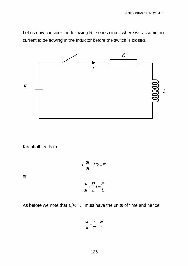
Circuit Analysis II WRM MT12
125
Let us now consider the following RL series circuit where we assume no
current to be flowing in the inductor before the switch is closed.
Kirchhoff leads to
ERidt
diL
or
L
Ei
L
R
dt
di
As before we note that TRL must have the units of time and hence
L
E
T
i
dt
di

126
which is mathematically, formally, equivalent to the differential equation
we previously encountered. The complementary function is again given
by
TtA exp
with time constant RLT and unknown constant A. The particular
integral is
R
E
L
TE
and hence the full solution
R
E
T
tAi exp
The initial condition, 00 i leads to R
EA and hence
T
t
R
Ei exp1
which again, has the standard form with a time constant, RLT .
It is left as an exercise to show that if we discharge the inductor through
the resistor that the current decays as T
t
R
Ei exp .

Circuit Analysis II WRM MT12
127
General remark
In the case of both the RC and RL circuits we have essentially solved a
first order differential equation with a time constant T. This led to a
complementary function for, say voltage, v, but it could equally be
current – it depends on the specific case – of the form
T
tAv exp
together with a particular integral giving the final steady state value, VSS
SSVv
The unknown constant, A, is determined by the initial condition 0vv .
Thus
SSVAv 0
or
v = [v(0+) – vSS].exp(-t/T) + VSS
or
v = [initial value – steady state value].exp(-t/T) + steady state value
or, in words,

128
the variable rises (falls) from its initial value to its final steady
state value exponentially with a time constant T

Circuit Analysis II WRM MT12
129
This observation permits us to sketch the transient response of many
simple circuits by inspection.
Initial Conditions
In order to sketch the transient response directly we need to be able to
find the voltage and current in a resistor, inductor and capacitor
immediately after a switch has been open or closed.
Resistor
Since the current and voltage are related by IRV it is clear that any
instantaneous change in, say, voltage will be accompanied by an equally
instantaneous change in current.
Inductor
Since the current and voltage are related by
dt
diLv
a sudden change in current would result in an infinite voltage. Since this
is implausible we can conclude that closing a switch to connect an
inductor to a source will not cause current to flow at the initial instant,
0t , i.e.
00 i
i.e. it will act as an open circuit.

130
If, of course, a current 0I was flowing before the switch was closed it will
continue to flow and
00 Ii
These observations permit us to introduce the idea of an equivalent
circuit at 0t
Capacitor
In this case
dt
dvCi
and arguments analogous to those above require that voltage does not
change instantly since the current cannot be infinite. If the capacitor is
initially uncharged then
00 v

Circuit Analysis II WRM MT12
131
i.e. the capacitor acts as a short circuit. If the capacitor is initially
changed to 0V
00 Vv
24. Example
If the capacitor is initially uncharged it acts like a short circuit at 0t
and hence

132
REi 0
The final steady state current is zero and hence the transient response
may be written as
RCtR
Eti exp
We note that if the resistance were small (zero) that ti would be very
large for a very short time. Although the 0R case could not happen in
practice it is often a useful "special case" and the discontinuity in current
is described by an impulse function, which has infinite magnitude for a
vanishingly short time.
As a further example we investigate the current flowing in the circuit
below after the switch is closed.

Circuit Analysis II WRM MT12
133
When the switch has been open long enough for the inductor to act as a
short circuit to DC a current 21 RREi and a time constant 1RLT
permits us to sketch

134
Second order transient
Consider
Kirchhoff gives
cvdt
diLRiE
which together with dt
dvCi c gives a second order differential equation
for the voltage across the capacitor as
LCd 2v
c
dt 2+RC
dvc
dt+v
c=E
We now solve the equation by our standard method of first obtaining the
complementary function by setting 0E on the right hand side and
looking for solutions of the form mtAexp . The auxiliary equation takes
the form

Circuit Analysis II WRM MT12
135
012 mRCmLC
which has solutions
LCL
R
L
Rm
1
42 2
2
In order to make some general comments we now recast this into non
circuit-specific notation following our discussion of resonance. In that
context we introduced
R
LQ
LC
00
1 and
We also noted that Q was related to the damping factor
L
CR
Q 22
1 via . This permits us to write
10
2m
or
m
with 0 and 120 .

136
We note that the particular integral, - corresponding to the steady value
of vc – is simply Evc . The full solution is therefore
ttBtAEvc expexpexp
where the unknown constants are determined by the initial conditions,
0cv and 0i . We note that the latter condition is formally equivalent
to requiring 0dt
dvc . The full solution now takes the form
tttE
Evc
expexpexp2
It is clear that according to the value of the factor may be real or
imaginary. We consider these cases in turn
Case 1: z >1; R>2 L C
In this case is real and >. It is convenient to write the solution
as
ttE
Evc
expexp2
where we see that the transient solution of the response is the difference
between two exponentials and is negative. The voltage cv follows the

Circuit Analysis II WRM MT12
137
usual gradual rise to its steady state value typical over overdamped
systems.
We note that the current is given by
dt
dvCi c
or
ttEC
i
expexp
2
20
Thus the current is proportional to the difference in two exponentials of
equal amplitude but different decay rates and hence rises from zero to a
maximum before finally falling to its steady state value of zero

138
Case 2: z =1 ; R=2 L C
For this special case of critical damping the general solution is no longer
valid since the auxiliary equation has two equal roots. The
complementary function in this case must take the form
tDtC 0exp
and hence the full solution becomes
tDtCEvc 0exp
which with initial conditions 0 ivc gives
ttEvc 00 exp11
which gives a response graphically similar to the previous case.

Circuit Analysis II WRM MT12
139
Case 3: z <1 ; R<2 L C
In this case becomes imaginary and so we write
njj 20
20 11
with
20 1 n
It is now straightforward to recast the general solution of page 136 by
replacing with nj as
tttEv n
n
nc expsincos1
In this case the solution is very different from before. The transient
solution is oscillatory, at a frequency n , but its amplitude decays at a
rate determined by 0 and we speak of underdamped oscillation.
The frequency 20 1 n is the natural frequency. The same term
is sometimes applied to 0 but the two are strictly only equal when 1
(critical damping).

140
(See HLT p169)
Case 4: z =0;R=0
In this case there is no damping since 0R means there is no element
in which energy can be dissipated. The voltage across the capacitor in
this undamped case is given by
tEvc 0cos1

Circuit Analysis II WRM MT12
141
We observe that for small damping, representing minimal loss, that the
frequency of the oscillatory transient 02
0 1 n , the resonance
frequency in the steady state. This is not surprising since this is the
frequency at which energy naturally oscillates between the reactive
elements and this is actually what is happening during transient
oscillation. Naturally with increased damping the effect is reduced.
We therefore see that the damping factor (or Q) has an important role
in describing the transient behaviour:
If the damping is less than critical (<1) the transient
behaviour is oscillatory otherwise it is not.

142
25. The Laplace Transform
The classical approach we have just used to find the transient response
and indeed the final steady state response for simple circuits may be
extended to ever more involved circuits but at the expense of ridiculously
increased complexity. An alternative approach is required. Since we
are concerned with turning forcing functions, often constants, on and off
the mathematical technique of choice to solve the differential equations
is based on the use of the Laplace transform. This is particularly useful
for our purposes because
(i) it gives rise to the ability to write circuit equations in a very general
way just as the "j" method does for sinusoidal forcing functions.
(ii) the initial conditions are dealt with automatically. The solution does
not contain any arbitrary constants.
(iii) Transients are dealt with automatically.
(iv) and, very importantly, the answers can be looked up easily in
H.L.T.!!
We recall that the Laplace transform of a function of time tf is
defined as
dtsttfsFtfL
exp0

Circuit Analysis II WRM MT12
143
where negative values of t are excluded. In mathematics since only
positive values of the variable t are permitted this is often called 'one-
sided' transform.
Arguably one of the most useful properties, from our point of view, of the
Laplace transform, is that for a given tf there is one and only one
sF and vice versa sF and tf are called transform pairs.
tfsF
Hence if we know the value of sF and we want to know tf , or vice
versa, we simply look it up in the tables!! What could be easier?
Although you will have worked out Laplace transforms in maths we'll
introduce a few 'electrically useful' transform pairs below.
(i) the unit step, tu
This function, which is useful to describe the closing of a switch say is a
function that switches from 0 abruptly to 1 at 0t . Thus the terminal
voltage in the circuit below would be written tu10

144
The Laplace transform sU is given by
s
dtstdtsttusU1
exp1exp00
Hence
s
tu1
are Laplace transform pairs. Thus given s
sU1
the corresponding
function of time is the unit step, tu .
(ii) exponential decay
0;exp tttf
sdttssF
1exp
0

Circuit Analysis II WRM MT12
145
(iii) damped sinusoids
0;sin
cosexp
t
t
tttf
Here it's probably easiest to consider the composite function
tjtjtttg expsincosexp
since this is formally equivalent to the exponential function we have just
discussed we can write the transform down directly as
222
1
sj
s
s
jssG
and hence by equating real and imaginary parts we find

146
2222
sinexp;cosexp
sttL
s
sttL
(iv) Laplace transform of a derivative
If the Laplace transform of tf is sF then
0fsFsdt
dfL
Where 0f represents the initial value of tf . The corresponding
expressions for the second derivative is
002
2
2
ffssFsdt
fdL
where f denotes the first derivative.
Fortunately for you in the P2 course (though not in the P1 course), we
will only use Laplace in the case of zero initial conditions when these
expressions simplify to
sFsdt
dfL
and sFs
dt
fdL 2
2
2
(v) Laplace transform of an integral
s
sFdttfL
t
0

Circuit Analysis II WRM MT12
147
Having listed a number of Laplace transforms let's now illustrate their
use formally by returning to the RC circuit we considered previously but
redrawn below
Since the switch is assumed to be closed at 0t the governing
differential equation may be written very generally as
tuT
E
T
v
dt
dv
Where, as before, RCT and the unit step 00 ttu and 1, 0t .
We now take Laplace transforms of all terms in the equation to give
sT
E
T
sVvsVs
1.0
If we assume, as before, that the capacitor is initially uncharged
00 v , gives

148
TssT
EsV
1
1.
The form of sV is almost familiar, but not quite. In order to be able to
find the inverse transform we need to rearrange it as
TssEsV
1
11
which are functions we have met before and permits us to transform
back to the time domain to give
TttuEtv exp
which, if we restrict ourselves to 0t , may be written in a more familiar
way as
TtEtv exp1
which is, of course, the solution we obtained previously but now with
considerably greater ease since we had no arbitrary constants to find.
We emphasise that the procedure involves
(i) transform the differential equation and include the initial conditions

Circuit Analysis II WRM MT12
149
(ii) manipulate the equation to obtain sV is an easily 'invertible' form.
This, sadly, may involve the use of partial fractions in more involved
cases.
(iii) transform back to the time domain to obtain tv .
It would be a useful exercise to return now to the second order RLC
circuit, transform the governing differential equation to obtain the
Laplace transform sVc of tvc with zero initial conditions as,
22
1
1
2
1
L
R
LCL
Rs
LRs
sEsVc
It is now routine – try it – to transform back to the time domain to
reproduce the damped and undamped cases we discussed previously.
We end this section by listing a further few useful properties of the
Laplace transform.

150
The Shifting theorem
We show below a function tf along with a "shifted" version. The
function Ttu is a unit step that is switched on at Tt .
If sF denotes the Laplace transform of tf then
sFsTTtuTtfL exp
i.e. when the time function is shifted along by T the Laplace transform is
multiplied by sTexp .
This property is very useful when building up the transforms of
complicated functions. Suppose we want to consider a pulse that might
correspond to the opening and subsequent closing of a switch. The time
function, tg , might look like

Circuit Analysis II WRM MT12
151
that is a unit step up at 0t together with a unit step down at Tt .
Thus
s
sT
s
sT
s
TtutuLtgL
exp1exp1
In reverse if we are required to find the inverse transform of, say,
22.exp
s
ssT
we recognise this as the inverse transform of 22
s
s, i.e.
tt cosexp but "shifted" by T. Thus the inverse transform is given by
TtTt
s
ssTL
cosexpexp
22
1

152
Thus we look up the transform in tables as usual and then introduce the
shifting function.
The tables which are available to you in the examination are to be found
in H.L.T. and are reproduced below for convenience.
Unit step at tut ,0 s1
!11 nt n
ns1
ate as 1
atea 11 ass 1
atcos 22 ass
atcosh 22 ass
atsin 22 asa
atsinh 22 asa
ata cos11 2 221 ass
atata sin1 3 2221 ass
atte 21 as
ate at 1 2ass
atatata cossin21 3 2221 as
atat sin2 222 ass
att cos 22222 asas
bte at cos 22
basas
bte at sin 22
basb

Circuit Analysis II WRM MT12
153
26. The Laplace transform in circuit analysis.
If we wanted to find how the voltage across a certain component varied
with time due to some arbitrary forcing function it would be perfectly
possible, using appropriate combinations of node-voltage and loop
equations, to set up the required (simultaneous) differential equations.
We could then take Laplace transforms of both sides of all the equations
or, to put it more technically, we would transform from the time domain to
the s-domain. The resulting simultaneous algebraic equations could
then be solved to find an expression for the Laplace transform of the
desired ‘output’ in terms of the Laplace transform of the ‘input’ source.
Once this frequency response function has been obtained it becomes a
routine matter to introduce the actual transform of the source and then
transform back to the time domain by looking up the inverse transforms
in tables. However it is possible to miss out the initial steps of writing the
differential equations and transforming them by working directly with
transformed voltages and currents V(s) and I(s) together with the
appropriate s-domain version of ‘Ohm’s Law’ for resistors, capacitors
and inductors.
Representation of circuit elements in the s-domain.
Resistor
The v-i equation for a resistor in the time domain is
iRv

154
The Laplace transform of this equation is
)()( sIRsV
The transfer function RsZsIsV )()(/)( is the s-domain impedance
of the element.
Inductor
In this case the time domain v-i relationship is
dt
diLv
which, when transformed into the s-domain assuming zero initial
conditions becomes
V(s) = sL I(s)

Circuit Analysis II WRM MT12
155
Capacitor
Finally we consider the v-i characteristics of a capacitor as
dt
dvCi
which becomes in the s-domain, assuming zero initial conditions,
I(s) = sC V(s)
or
V(s) = (1/sC) I(s)
I hope that, by now, although this approach is new, it is beginning to feel
a little familiar. When we were interested in sinusoidal sources (forcing
functions) we found that the mathematical technique which enabled us
to solve the differential equations most easily required us to write ‘Ohm’s
Law’ for the resistor, inductor and capacitor, in phasor notation as

156
ICj
1VandILjVIRV
respectively. In the more general s-domain case the relationships are
IsC
1VandIsLVIRV
which are seen to be identical if we merely replace j by s. Thus all
the methods we developed in the AC theory ‘j’ case carry over to the s-
domain by simple substitution.
Example
Let’s revisit the RC circuit we have already analysed twice before
already i.e.
Where )()(1 tuEtv since the switch is closed at t=0. Since the
capacitor is assumed to be uncharged the circuit may be redrawn s-
domain notation below. We have also re-arranged the circuit to make it
clearly of the form of a voltage divider.

Circuit Analysis II WRM MT12
157
We can immediately write
sVsCR
sV
sCR
sCsV
1
12
1
1
1
1
which, introducing T = RC and sEsV /)(1 gives
sTs
EsV
1)(2
which is the same function we obtained previously but we have found it
much more easily and directly here.
As a further example consider the circuit below together with its s-
domain representation.

158
In this case
sV
sCR
RsV 12 1)(
which with sEsV /)(1 and T = RC gives
Ts
EsV
1)(2
The inverse is readily looked up in tables to give
TtEtv /exp)(2
We know, from physical reasoning, that when the switch opens,
Ev )0(2 , whereas when it has been open for a long time the capacitor
acts as an open circuit and hence 0)(2 v . These observations are
confirmed, of course, by the expression we have just obtained. However
it can also be checked from the form of V(s) by using the initial and final
value theorems. We know

Circuit Analysis II WRM MT12
159
EsT
ELim
Ts
sELimssVLimvalue initial sss
11
)(2
whereas the final value is given by
01
)( 020
Ts
sELimssVLimvalue final ss
We note the procedure is
(i) Introduce ‘generalised’ s-domain impedances, sL and 1/sC.
(ii) Find the appropriate transfer function. In more complicated cases
this may/will involve writing node-voltage and/or loop equations.
(iii) Substitute the Laplace transform of the input signal (forcing
function)
(iv) Convert back to the time domain by looking up the inverse
transforms in tables.
As a final example let’s consider the following circuit where the input
voltage is a pulse of duration T and we are required to find the voltage
)(2 tv .

160
The generalised impedance of the RC parallel combination is given by
CRsR 1/ and hence, after a little trivial algebra
111
2
/1
1
2
1
TsTsV
sV
where T1 = CR/2.
We have already shown how the shift theorem may be used to obtain
the Laplace transform of a pulse by regarding it as the superposition of
two time-delayed step functions. The details were given previously
which permit us to write
sTs
EsV exp11
and hence

Circuit Analysis II WRM MT12
161
sTTss
E
sTsTssT
EsV
exp1/1
11
2
exp1/1
1
2
1
11
2
The inverse of the expression in curly brackets is readily obtained as
1/exp)( Tttu . The second bracket merely indicates, as we have
seen before that the full solution consists of the difference between two
identical, but time shifted, expressions. Thus
112 /)(exp)(/exp)(2
TTtTtuTttuE
tv
which, depending on the relationship between T and T1, might look
something like

162
27. Disclaimer!!
The notes are reasonably self-contained but they certainly don’t pretend
to tell the whole story so please do consult one or more of the huge
number of textbooks on the subject.