charging effects on sem/sim contrast of … effects on sem/sim contrast of metal/insulator system...
TRANSCRIPT

Charging Effects on SEM/SIM Contrast of Metal/Insulator System
in Various Metallic Coating Conditions
Ki Hyun Kim1;*, Zentaro Akase1, Toshiaki Suzuki2 and Daisuke Shindo1
1Institute of Multidisciplinary Research for Advanced Materials, Tohoku University, Sendai 980-8577, Japan2JEOL Ltd., Tokyo 196-8558, Japan
Scanning electron microscope (SEM) and scanning ion microscope (SIM) observations were performed to investigate the charging effectand the related contrast variation for images of conductive and non-conductive specimens under electron and Gaþ ion beam irradiations. Thecontrast variation in the specimens was investigated by changing the coating conditions. It was found that the contrast in conductive specimenswas basically caused by differences in atomic number and that the charging effect in conductive specimens is generally smaller than that in non-conductive specimens. On the other hand, the SEM contrast of non-conductive specimens varied widely, depending on the coating conditions.These contrast variations were found to be caused by negative charges accumulated on the surface of the specimens. The SIM contrast of non-conductive specimens changed to dark when the coating condition was insufficient. The contrast variations were found to be caused by theaccumulation of positive charges on the surface of specimens. [doi:10.2320/matertrans.M2010034]
(Received January 27, 2010; Accepted March 26, 2010; Published May 19, 2010)
Keywords: charging, osmium (Os) coating, scanning electron microscopy (SEM)/scanning ion microscopy (SIM) contrast
1. Introduction
Electron/ion microscopy techniques have been widelyemployed for the characterization of various specimens suchas metals, insulators, and polymers. Among the manymicroscopic techniques, scanning electron microscopy(SEM) and focused ion beam (FIB) techniques have beenextensively employed in the fields of materials science.1,2)
The formation of image contrast by these techniques isattributed to secondary electrons excited on the specimensurface by the incident electron and Gaþ ion beamirradiations. These electron- and ion-induced secondaryelectron images can be used for surface analysis of variousspecimens. Therefore, the yield of secondary electronsemitted from specimens is an important factor for reliableinterpretations of image contrast.3,4)
In recent years, many studies have focused on interpretingSEM and scanning ion microscopy (SIM) image contrasts.5–7)
In the case of conductive specimen, the dependence ofsecondary electron yield on the atomic number of a specimenhas been investigated. The results of these studies haveshown that the secondary electron yield in SEM tends toincrease with an increase in the atomic number. On the otherhand, the secondary electron yield in SIM decreases with anincrease in the atomic number. It has been explained that thistendency is caused by the difference between the penetrationdepths of ion and electron beams.5–7)
When the SEM or SIM contrast of a non-conductivespecimen is interpreted, the charging effect arising fromelectron/ion irradiation is unavoidable. In general, thecharging effect is caused by the accumulation of staticelectric charges on the specimen surface, which results inmany problems.8–11) For example, the negative chargewould flip the secondary electron from the surface. Thenegative charge would also reduce the landing energy of theincident electrons, and it would increase the field between
the surface and secondary electron detector. On the otherhand, positive charge would re-collect the secondaryelectron.12) In order to discuss the secondary electronemission from non-conductive specimen quantitatively, amodel have been presented.13,14) It shows the yield is notonly a function of the chemical composition but alsofunctions of the specimen structure, temperature and theirradiation conditions. Consequently, reliable evaluation ofSEM/SIM images of non-conductive specimens is difficult.For reliable analysis, in addition to the suppression of thecharging effect through the use of a metallic coating,evaluating how the charging effect is suppressed by themetallic coating is also important.
In this study, we investigated the change of SEM and SIMimage contrasts of conductive and non-conductive specimenswith various metallic coating conditions in order to evaluatehow the charging effect appears on those specimens. Weselected an Al2O3 sintered body, tungsten (W), and alumi-num (Al) as typical non-conductive and conductive speci-mens. Those specimens were prepared with osmium (Os)coating under several conditions.
2. Experimental Methods
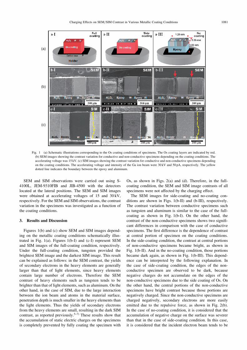
Figure 1(a) shows a schematic illustration indicatingthe coating conditions of the specimens. Here, an Al2O3
sintered body was prepared by a pressureless sinteringmethod at 1600�C using commercial Al2O3 powder (AKP-50, Sumimoto).15) For conductive specimens, commercialaluminum and tungsten were used. These specimens weremounted in epoxy resin which was fixed at room temperaturefor 12 h; the mounted specimens were then sectioned usinga diamond saw and thinned using SiC grinding paper. Thesize of the prepared specimens is indicated in Fig. 1(a). Thespecimens were coated with 2 nm of Os using a commercialOs plasma coater (OPC60A, Filgen Inc.). Figures 1(a-I)–(a-III) show the coating conditions for specimens corre-sponding to full-coating, side-coating, and no-coating,respectively.
*Present address: Nanostructures Research Laboratory, Japan Fine
Ceramics Center, Nagoya 456-8587, Japan
Materials Transactions, Vol. 51, No. 6 (2010) pp. 1080 to 1083#2010 The Japan Institute of Metals
SEM and SIM observations were carried out using S-4100L, JEM-9310FIB and JIB-4500 with the detectorslocated at the lateral positions. The SEM and SIM imageswere obtained at accelerating voltages of 15 and 30 kV,respectively. For the SEM and SIM observations, the contrastvariation in the specimens was investigated as a function ofthe coating conditions.
3. Results and Discussion
Figures 1(b) and (c) show SEM and SIM images depend-ing on the metallic coating conditions schematically illus-trated in Fig. 1(a). Figures 1(b-I) and (c-I) represent SEMand SIM images of the full-coating condition, respectively.Under the full-coating condition, tungsten provided thebrightest SEM image and the darkest SIM image. This resultcan be explained as follows: in the SEM contrast, the yieldsof secondary electrons in the heavy elements are generallylarger than that of light elements, since heavy elementscontain large number of electrons. Therefore the SEMcontrast of heavy elements such as tungsten tends to bebrighter than that of light elements, such as aluminum. On theother hand, in the case of SIM, due to the large interactionbetween the ion beam and atoms in the material surface,penetration depth is much smaller in the heavy elements thanthe light elements. Thus the yields of secondary electronsfrom the heavy elements are small, resulting in the dark SIMcontrast, as reported previously.5–7) These results show thatthe accumulation of static electric charges on the specimensis completely prevented by fully coating the specimen with
Os, as shown in Figs. 2(a) and (d). Therefore, in the full-coating condition, the SEM and SIM image contrasts of allspecimens were not affected by the charging effect.
The SEM images for side-coating and no-coating con-ditions are shown in Figs. 1(b-II) and (b-III), respectively.The contrast variation between conductive specimens suchas tungsten and aluminum is similar to the case of the full-coating as shown in Fig. 1(b-I). On the other hand, thecontrast of the non-conductive specimens shows two signifi-cant differences in comparison with the case of conductivespecimens. The first difference is the dependence of contrastat central portion of specimen on the coating conditions.In the side-coating condition, the contrast at central portionsof non-conductive specimens became bright, as shown inFig. 1(b-II). And in the no-coating condition, those portionsbecame dark again, as shown in Fig. 1(b-III). This depend-ence can be interpreted by the following explanation. Inthe case of side-coating condition, the edges of the non-conductive specimen are observed to be dark, becausenegative charges do not accumulate on the edges of thenon-conductive specimens due to the side coating of Os. Onthe other hand, the central portions of the non-conductivespecimens have bright contrast because those portions arenegatively charged. Since the non-conductive specimens arecharged negatively, secondary electrons are more easilyemitted due to the repulsive force, as shown in Fig. 2(b).In the case of no-coating condition, it is considered that theaccumulation of negative charge on the surface was severerthan that in the case of side-coating condition. In this case,it is considered that the incident electron beam tends to be
(a)
(b)
(c)
Fig. 1 (a) Schematic illustrations corresponding to the Os coating conditions of specimens. The Os coating layers are indicated by red.
(b) SEM images showing the contrast variation for conductive and non-conductive specimens depending on the coating conditions. The
accelerating voltage was 15 kV. (c) SIM images showing the contrast variation for conductive and non-conductive specimens depending
on the coating conditions. The accelerating voltage and intensity of the Ga ion beam were 30 kV and 50 pA, respectively. The yellow
dotted line indicates the boundary between the epoxy and aluminum.
Charging Effects on SEM/SIM Contrast in Various Metallic Coating Conditions 1081

deflected due to the severe charge accumulation on thesurface as shown in Fig. 2(c). Thus, the number of thesecondary electrons emitted from the specimen may decreasedue to the decrease of incident electrons landing to thespecimen. The second difference is that abnormal darkcontrasts appeared in tungsten and aluminum, as indicated byred arrows in Fig. 1(b-III). It is noted that the edge part of theabnormal dark contrast is narrow, and the middle part is wide.It is considered that the edges of abnormal dark contrastswere partially compensated for by leakage of electrons intothe substrate (earth). On the other hand, in the middle regionof the abnormal dark contrasts, the secondary electrons wereaffected by a severe charging effect in epoxy. Since theelectron beam is scanned on the specimen from the left to theright, it is considered that the regions on the right of epoxytend to be more affected by the charging effect. The widthof the dark contrast is small. This may be due to the thinthickness of the epoxy near the aluminum. In order tounderstand the change of SEM contrast due to the chargingeffect and abnormal contrast accurately, further experimentwith electric field analysis will be carried out in future.
The SIM images for side-coating and no-coating con-ditions are shown in Figs. 1(c-II) and (c-III), respectively. Inthe side-coating condition shown in Fig. 1(c-II), the contrastvariation between conductive specimens is similar to the caseof the full-coating as shown in Fig. 1(c-I). However, in theno-coating condition shown in Fig. 1(c-III), the contrastsof tungsten became brighter than that of aluminum. Thiscontrast variation is different from those cases in the full-coating and the side-coating conditions. The reason can beexplained as follows. In the no-coating condition, theconductive specimens are isolated from the substrate electri-cally, as shown in Fig. 1(a-III). Thus, positive chargesaccumulate even on the surface of conductive specimens dueto the Gaþ ion implantation. If there is no accumulation ofpositive charges, the penetration depth in aluminum is widerthan that in tungsten. But the accumulation of positive
charges limits the penetration depths of both specimens to thesurface region only. Considering that tungsten has moreelectrons than aluminum as discussed above, the contrast oftungsten becomes relatively brighter than that of aluminumdue to the higher probability of secondary electron emission.On the other hand, in the case of non-conductive specimens,the contrasts in the side-coating and no-coating conditionsbecame darker than that in the full-coating condition. It isconsidered that these variations are attributed to positivecharging, since for SIM images of the side-coating and no-coating conditions, non-conductive specimens are positivelycharged due to Gaþ ion implantation. Consequently, thesecondary electrons emitted from the specimen are attractedto the surface of the positively charged specimen, as shownin Figs. 2(e) and (f) which is consistent with the discussionin the reference.3)
Finally, we should note that the contrast variations notedabove were found to have the same tendency when weobserved specimens with SEM at an accelerating voltage of10 kV and with SIM at accelerating voltages of 15 and 20 kV.
4. Conclusion
The findings of this study on the charging effect and therelated contrast variation under electron and ion beamirradiation can be summarized as follows:
(1) The contrast of SEM and SIM images is basicallycaused by the difference in atomic number of the specimensbecause the atomic number is related to the penetration depthof conductive specimens for electron and ion irradiation.However, when the coating was insufficient, the contrastof non-conductive specimens could not be explained by theatomic number. The contrast was found to strongly dependon the charging effect and metallic coating conditions.
(2) Depending on the state of coating conditions, thecontrasts of non-conductive specimens in the SEM imageswere changed. This result indicates that these contrast
(a) (b) (c)
(d) (e) (f)
Fig. 2 Schematic illustration of secondary electron emission for non-conductive specimens depending on the coating conditions. (a)–(c)
Schematic illustrations for an SEM under electron beam irradiation. (d)–(f) Schematic illustrations for an SIM under Ga ion beam
irradiation. The Os coating layers are indicated by red lines.
1082 K. H. Kim, Z. Akase, T. Suzuki and D. Shindo

variations are caused by accumulated negative charges on thesurface of specimens. On the other hand, the contrasts in theSIM image became dark when the charging effect occurred.This result reveals that the contrast of non-conductivespecimens can be attributed to positive charges accumulatedon the surface of specimens due to Gaþ ion beam irradiation.
Acknowledgements
The authors are grateful to Mr. A. Ono and Mr. S. Ikeda fortheir useful discussion.
REFERENCES
1) S. Reyntjens and R. Puers: J. Micromech. Microeng. 11 (2001) 287–
300.
2) Z. L. Wang, Y. Liu and Z. Zhang: Handbook of nanophase and
nanostructured materils Volume II: Characterization, (Kluwer Aca-
demic/Plenum Publishers, New York, 2003).
3) L. A. Giannuzzi and F. A. Stevie: Introduction to focused ion beams:
instrumentation, theory, techniques and practice, (Springer, New York,
2004) p. 258.
4) H. Seiler: J. Appl. Phys. 54 (1983) 1100R1–R18.
5) Y. Sakai, T. Yamada, T. Suzuki, T. Sato, H. Itoh and T. Ichinokawa:
Appl. Phys. Lett. 73 (1998) 611–613.
6) Y. Sakai, T. Yamada, T. Suzuki and T. Ichinokawa: Appl. Surf. Sci.
144–145 (1999) 96–100.
7) T. Suzuki, N. Endo, M. Shibata, S. Kamasaki and T. Ichinokawa:
J. Vac. Sci. Technol. A 22 (2004) 49–52.
8) K. Ura and S. Aoyagi: J. Electron Microsc. 49 (2000) 157–162.
9) K. Ura: J. Electron Microsc. 47 (1998) 143–147.
10) M. Fukuda, S. Tomimatsu, H. Shichi and K. Umemura: Microelectron.
Eng. 78–79 (2005) 22–28.
11) K. H. Kim, J. J. Kim, T. Suzuki and D. Shindo: J. Electron Microsc. 57
(2008) 53–57.
12) D. C. Joy and C. S. Joy: Micron 27 (1996) 247–263.
13) J. Cazaux: Ultramicrosc. 108 (2008) 1645–1652.
14) J. Cazaux: Microsc. Microanal. 10 (2004) 670–684.
15) B. T. Lee, I. C. Kang, S. H. Cho and H. Y. Song: J. Am. Ceram. Soc. 88
(2005) 2262–2266.
Charging Effects on SEM/SIM Contrast in Various Metallic Coating Conditions 1083