charge transport mechanism in thin cuticles holding nandi flame
TRANSCRIPT

Hindawi Publishing CorporationInternational Journal of BiomaterialsVolume 2009, Article ID 548406, 9 pagesdoi:10.1155/2009/548406
Research Article
Charge Transport Mechanism in Thin Cuticles HoldingNandi Flame Seeds
Wycliffe K. Kipnusu,1 Gabriel Katana,1 Charles M. Migwi,1
I. V. S. Rathore,1 and Joshua R. Sangoro2
1 Physics Department, Kenyatta University, P.O. Box 43844-00100, Nairobi, Kenya2 Institute of Experimental Physics I, University of Leipzig, 04103 Leipzig, Germany
Correspondence should be addressed to Wycliffe K. Kipnusu, [email protected]
Received 20 January 2009; Accepted 25 May 2009
Recommended by Aldo Boccaccini
Metal-sample-metal sandwich configuration has been used to investigate DC conductivity in 4 μm thick Nandi flame [Spathodeacampanulata P. Beauv.] seed cuticles. J-V characteristics showed ohmic conduction at low fields and space charge limited currentat high fields. Charge mobility in ohmic region was 4.06× 10⁻⁵ (m2V−1s−1). Temperature-dependent conductivity measurementshave been carried out in the temperature range 320 K < T > 450 K. Activation energy within a temperature of 320 K–440 K wasabout 0.86 eV. Variable range hopping (VRH) is the main current transport mechanism at the range of 330–440 K. The VRHmechanism was analyzed based on Mott theory and the Mott parameters: density of localized states near the Fermi-level N(EF) ≈9.04 × 10¹⁹ (eV−1cm−3) and hopping distance R ≈ 1.44 × 10⁻⁷ cm, while the hopping energy (W) was in the range of 0.72 eV–0.98 eV.
Copyright © 2009 Wycliffe K. Kipnusu et al. This is an open access article distributed under the Creative Commons AttributionLicense, which permits unrestricted use, distribution, and reproduction in any medium, provided the original work is properlycited.
1. Introduction
A recent surge in interest in molecule-based electronics hashighlighted the need for a better understanding of con-duction mechanism in biomaterials [1]. Most biomaterialsare obtained from plant products. Plant cuticle membraneshave been found to contain high proportions of insolubleand acid resistant cutin biopolyester [2]. Current-voltagecharacteristics of Nandi flame seed cuticle biomaterial haveshown electrical switching and memory properties [3].Conducting biomaterials have been demonstrated to bepotentially useful in making eco-friendly electronic devicesand probes for sensors fabrication [4–7], solid electrolytesystems [8], barrier materials, and controlled release poly-mers [9], and in tissue engineering because they can easilybe used as a platform that supports electrical stimulation ofcell-tissue constructs [10].
Generally charge conduction in semiconducting poly-mers is thought to take place by hopping of charge carriers inan energetically disordered landscape [11]. VRH conductionmechanism originally proposed by Mott for amorphous
semiconductors [12] assuming a phonon-assisted processhas been employed in previous studies [13–15] to explaincharge transport in conducting synthetic polymers and theircomposites at low temperatures. Hopping charge transporthas also been noted in double helix DNA [16] and in ion-doped biopolymers [8, 17].
While considerable time has been devoted to investigateconduction mechanism in synthetic polymers [18–23], onlylittle attention has been paid towards electrical conductivityof pristine biopolymers. Consequently, there are notablyfew studies that can reliably explain conductance obser-vations made with biopolymers [10]. Davis [1] suggestedthat electron and resonance tunneling is responsible fordetectable charge transport in biomolecules sandwichedbetween metal electrodes. From measurements that probedchanges in oxidized guanine damage yield with response tobase perturbations, Armitage et al. [24] noted that chargetransfer through base-base of DNA molecules takes placevia the π-π bond overlap. Tao et al. [25] reported electronand bridge-assisted super-exchange charge transfer betweendonor and acceptor groups in peptide systems. Similar

2 International Journal of Biomaterials
studies on proteins have also shown that electron transfercan occur across hydrogen bonds and that the rate of suchtransfer is greatly increased when the electron motions arestrongly coupled with those of the protons [26]. Radhaand Rossen [27] studied energy transport in biopolymersand suggested, based on the experimental results, that asoliton in biopolymers is an energy packet (similar to the“conformon” which is the packet of conformational strainon mitochondria) associated with a conformational strainlocalized in region much shorter than the length of amacromolecule. It was noted that as the soliton (localizedcurvature) moves on the polymer, it could trap an electronand drag it along. This mechanism may be importantin understanding charge transport in biological molecules,where curvatures abound.
In this paper, we report dc conductivity measurementsand charge transport mechanisms in Nandi flame seedcuticle (a pristine biopolymer) in the temperature range 350–450 K. Fourier transform infrared (FT-IR) spectra analysis ofpristine Nandi flame seed cuticle in comparison with FT-IRspectra of cellulose and surface probe analysis using atomicforce spectroscopy (AFM) are presented before electricalconductivity. Discussion of charge transport mechanism ispresented based on the fact that at least one mechanism canpredominate within a specific temperature range. The fol-lowing charge transfer mechanisms: electric field dependentSchottky and Poole-Frenkel emission, space charge limitedcurrent (SCLC) (from which some electrical parameters ofthe sample are obtained), tunneling current, and VRH arediscussed in that order.
2. Experimental
Samples of thin seed cuticles (Figure 1) were obtained fromNandi flame trees, also known as African tulip, which areused as ornamental trees in Kenya. Samples were well cleanedwith acetone and dried at a temperature of 310 K for 12 hoursinside a Lindberg blue tube furnace of model TF55035Cand then stored in polythene bags containing silica geldesiccators. FT-IR studies were done in order to compare theIR spectrum of the cuticle to that of cellulose. Samples forFT-IR measurement were prepared by grinding the sample(0.1–2.0 percent by weight) with Potassium Bromide (KBr)and compressing the whole into a wafer. Thickness of thesamples was determined by an interferometric method [28]and found to be about 4 μm. Electrode coating on thefilm of pristine cuticles was done using quick drying andhighly conducting flash-dry silver paint obtained from SPISupplies, Pa, USA. A mask (made of stiff and thin transparentpolythene paper) of circular aperture of 0.56 cm diameterwas used while coating, to ensure uniformity in size of coatedsurface. Circular aluminum foil of the same diameter wasplaced on freshly coated surface such that the sample wassandwiched between two aluminum electrodes. These metal-cuticle-metal sandwiches were left to dry at room tempera-ture for a period of 24 hours to ensure that there was goodohmic contacts between aluminum electrode and the samplecuticle. Flash-dry Silver paint was used to connect thermally
Figure 1: Translucent and thin cuticle holding Nandi flame seed.
insulated thin wires onto the aluminum electrodes. A cuticlesandwiched between aluminum electrodes was placed insidethe Lindberg/Blue Tube Furnace and temperature varied atsteps of 5 K between 350 K and 500 K at constant electricfields while measuring current-Voltage (I-V) using Keithley2400 series source meter.
Surface structural characterization of the pristine cuti-cles was done using AFM (a Digital Instrument Multi-mode/Nanoscope III scanning probe microscope was used).Taking images at the fundamental resonance frequency of Sicantilevers (≈300 kHz) while operating the instrument in thetapping mode, the height and phase images were obtainedsimultaneously.
3. Results and Discussion
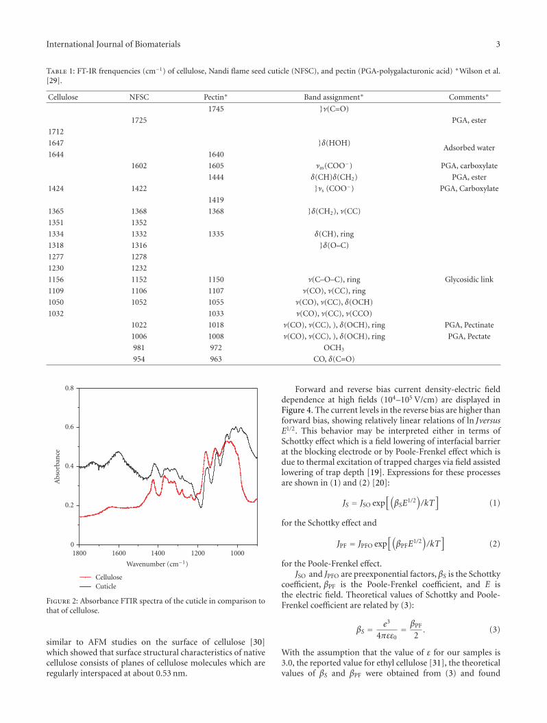
The FT-IR spectra of the cuticle and cellulose are shownin Figure 2. The IR bands (given with accuracy of 2 cm−1)and band assignments are listed in Table 1. Cellulose IR databands and comments in Table 1 are based on literature [29].Vibrations in the 1800 to 1200 cm−1 range mostly arise fromside chains or side groups (such as ester and OH) whilevibration in the 1200 to 900 cm−1 are related to backbonesof polysaccharides such as cellulose, hemicelluloses, andpectin [29]. The strong IR bands of the cuticle at 1278 cm−1
assigned to δ (CH), and 1106 cm−1 assigned to ν(CO), ν(CC)are overlapped with strong cellulose bands at 1277 cm−1 and1107 cm−1, respectively. Generally, the cuticle IR bands inthe range 1050 to 1400 cm−1 are strongly correlated withthe bands of cellulose. This therefore means that the cuticlebackbone molecules are composed of cellulose. However,IR absorption peaks of the cuticle in the carbonyl sidegroup region (1750–1600 cm−1) and in the region relatedto backbone of polysaccharides (1025–950 cm−1) do notcorrespond to cellulose bands.
Figures 3(a) and 3(b) are AFM scans showing surfacestructural characteristics of the cuticle sample. The AFMtopographic scan shows that the cuticle has a highly orientedsurface topography. The interstitial regions between theridges represented by dark area are cavities on the membranehaving an approximate width of 0.5 nm. This results are
International Journal of Biomaterials 3
Table 1: FT-IR frenquencies (cm−1) of cellulose, Nandi flame seed cuticle (NFSC), and pectin (PGA-polygalacturonic acid) ∗Wilson et al.[29].
Cellulose NFSC Pectin∗ Band assignment∗ Comments∗
1745 }ν(C=O)
1725 PGA, ester
1712
1647 }δ(HOH)Adsorbed water
1644 1640
1602 1605 νas(COO−) PGA, carboxylate
1444 δ(CH)δ(CH2) PGA, ester
1424 1422 }νs (COO−) PGA, Carboxylate
1419
1365 1368 1368 }δ(CH2), ν(CC)
1351 1352
1334 1332 1335 δ(CH), ring
1318 1316 }δ(O–C)
1277 1278
1230 1232
1156 1152 1150 ν(C–O–C), ring Glycosidic link
1109 1106 1107 ν(CO), ν(CC), ring
1050 1052 1055 ν(CO), ν(CC), δ(OCH)
1032 1033 ν(CO), ν(CC), ν(CCO)
1022 1018 ν(CO), ν(CC), ), δ(OCH), ring PGA, Pectinate
1006 1008 ν(CO), ν(CC), ), δ(OCH), ring PGA, Pectate
981 972 OCH3
954 963 CO, δ(C=O)
0
0.2
0.4
0.6
0.8
Abs
orba
nce
1800 1600 1400 1200 1000
Wavenumber (cm−1)
CelluloseCuticle
Figure 2: Absorbance FTIR spectra of the cuticle in comparison tothat of cellulose.
similar to AFM studies on the surface of cellulose [30]which showed that surface structural characteristics of nativecellulose consists of planes of cellulose molecules which areregularly interspaced at about 0.53 nm.
Forward and reverse bias current density-electric fielddependence at high fields (104–105 V/cm) are displayed inFigure 4. The current levels in the reverse bias are higher thanforward bias, showing relatively linear relations of ln JversusE1/2. This behavior may be interpreted either in terms ofSchottky effect which is a field lowering of interfacial barrierat the blocking electrode or by Poole-Frenkel effect which isdue to thermal excitation of trapped charges via field assistedlowering of trap depth [19]. Expressions for these processesare shown in (1) and (2) [20]:
JS = JSO exp[(βSE
1/2)/kT
](1)
for the Schottky effect and
JPF = JPFO exp[(βPFE
1/2)/kT
](2)
for the Poole-Frenkel effect.JSO and JPFO are preexponential factors, βS is the Schottky
coefficient, βPF is the Poole-Frenkel coefficient, and E isthe electric field. Theoretical values of Schottky and Poole-Frenkel coefficient are related by (3):
βS = e3
4πεε0= βPF
2. (3)
With the assumption that the value of ε for our samples is3.0, the reported value for ethyl cellulose [31], the theoreticalvalues of βS and βPF were obtained from (3) and found

4 International Journal of Biomaterials
(a)
(b)
Figure 3: AFM topographic scans showing surface structure of thecuticle; (a) is a map from the scan on a larger area of about 3× 10⁵
square pixels (b) is a scan on a single pixel of about 2.5 × 10⁶ nm2.Doted lines on (a) represents the region shown by (b). scale bars∼0.5 nm.
Table 2: Values of β obtained from experimental data.
Temperature (K)Experimental β (Jm1/2 V1/2) values
Forward bias Reverse bias
320 5.65× 10⁻²³ 3.17× 10⁻²³
350 6.31× 10⁻²³ 3.56× 10⁻²³
370 3.44× 10⁻²³ 0.93× 10⁻²³
to be 3.51 × 10⁻²⁴ J V1/2 m1/2 and 7.01 × 10⁻²⁴ J V1/2 m1/2,respectively. Experimental values of β obtained from slopes(linear regression parameters) of linear fit plots of ln Jversus E1/2 (Figure 4) at different temperatures are listed inTable 2. The large discrepancy in experimental values of βlisted in Table 2 and theoretical values of βS and βPF leads to aconclusion that current transport mechanism in our samplesgoverning the high field at a temperature range of 320–370 Kcannot be explained in terms of Shottky or Poole-Frenkelemission.
Figures 5(a) and 5(b) show J-V characteristics over atemperature range of 320–350 K for the forward bias andreverse bias, respectively. Figure 5(a) shows that forward biascharacteristics has two regions: low voltage region below athreshold voltage (Vth) where current density follows ohmslaw relations (ohmic region), and higher voltages region,
−11
−10
−9
−8
−7
−6
−5
−4
lnJ
(Acm
−2)
180 200 220 240 260 280 300 320
E1/2(V/vm)
320 K forward bias350 K forward bias400 K forward bias
320 K reverse bias350 K reverse bias400 K reverse bias
Figure 4: Semilogarithmic plots of ln J versus E1/2 for the highfield of 104–105 V/cm in forward bias (increasing electric field) andreverse bias (decreasing electric field) and poling temperature range320 K–370 K (R-reverse bias; F-forward bias).
above Vth at which, there is a pronounced power-law behav-ior given by JαVn where n ≈ 1.8 ± 0.3 (SCLC region). Vth
has negative temperature coefficient as noticed in Figure 5(a)where it decreases as temperature increase—a case that isidentical to tunneling of charge carriers through the entiremetal-insulator-metal junction for a structure with multipletunnel barriers in the Coulomb blockade regime [32]. Ata poling temperature of 400 K, Vth decreased leading to asmooth transition from low ohmic region to SCLC. Existenceof Vth elucidates electrical switching of the material fromhigh impedance region where the current densities are verylow, to low impedance region which allows large currents toflow. Figure 5(b) shows that our samples remained in the lowimpedance region even as the voltage was decreased (reversebias) leading to high levels of leakage current in the reversebias than in the forward bias (see Figure 4). This can alsobe explained in terms of built up of image charges at highfield of the reverse bias which lowers potential barrier atthe metal-polymer junction hence allowing higher current toflow in the reverse bias [21]. This phenomenon of electricalswitching with memory has also been observed in somesynthetic polymers [33–36] and has been used as active cellsin modern nonvolatile memory chips [37]. Polymers whichexhibit electrical switching and memory effect can also beapplied in electrical switching circuit and in gas sensing [36].Electrical switching is explained in terms of formation ofsemiquinones and quinoid radicals [3] and in terms of SCLC.As shown in Figure 5(a), the low current densities at lowvoltages is due to charge capture in traps (intrinsic charges)

International Journal of Biomaterials 5
present in the cuticle. Increase in bias voltage results inan increase in injected charge, thereby filling the limitedtraps. This injection is provided by tunneling of the electrons(holes) into the conduction (valence) bands of the polymer.Injection of charges from metal electrode causes a reductionin the number of traps which, leads to a rapid increasein effective carrier mobility and therefore a rapid power-law increase in current. At sufficiently high injection levels,all the traps are filled reaching the trap filled limit (TFL)and consequently the current becomes SCLC. The total trapconcentration Nt in the cuticle sample is defined in (4) [31]:
Nt = 2εε0
ed2VTFL, (4)
where e is the electronic charge ε relative permittivity of thematerial ε0 is the permittivity of free space, d is thickness ofsample (4 μm) and, VTFL is the upper limit of the voltage atwhich sufficient charge has been injected into the insulatorto fill the traps. Equilibrium carrier concentration n0 can beobtained from the expression (5) [38]:
n0 = 98εε0
ed2Vtr, (5)
where Vtr is the voltage at which the transition from ohmicto SCLC behavior takes place. Using experimental values ofVTFL = 15 V and Vtr = 6 V obtained from J-V curve at320 K (Figure 5(a)), the values of Nt and n0 were calculatedfrom (4) and (5). Current density at low voltage (the ohmicconduction region) is given by (6):
J = p0eμV
d, (6)
where p0 is the concentration of thermally activated holesexpressed as shown in (7):
p0 = NV exp(− EdkT
). (7)
Current density then becomes
J = NveμV
d exp(Ed/kT), (8)
where Nv is effective density of states, e is electron charge, μis charge mobility, V is the applied voltage, d is the samplethickness, Ed is the ionization energy of donor charges, kis the Boltzmann’s constant, and T is the temperature. Byplotting ln J versus 1000/T it is possible to determine μ andEd. Variation of ln J with 1000/T, at a voltage of 0.9 V (ohmicregion) is shown in Figure 6. Assuming that Nv = 1019 cm−3
which is within the range of the effective density of states forthin films of other organic semiconductors [39], the valueof po, μ, and Ed are determined from (7) and (8). Theseelectrical parameters, po, μ, and Ed being obtained from anal-ysis of temperature dependence of ohmic region and Nt, n0
obtained from analysis of SCLC regime are listed in Table 3.The low charge mobility and the electrical parameters shownin Table 3 are comparable to same parameters calculated forother organic semiconductors [31, 38].
−10
−9
−8
−7
−6
−5
−4
−3
−2
−1
logJ
(Acm
−2)c
ot
0 10 20 30 40
Voltage (V)
320 K350 K400 K
(a)
−8
−7
−6
−5
−4
−3
−2
logJ
(Acm
−2)
−5 0 5 10 15 20 25 30 35 40
Voltage (V)
320 K350 K400 K
(b)
Figure 5: (a) Semilogarithmic plots of log J versus V as a function ofpoling temperature in the forward bias regime. (b) Semilogarithmicplots of log J versus V as a function of poling temperature in thereverse bias regime.
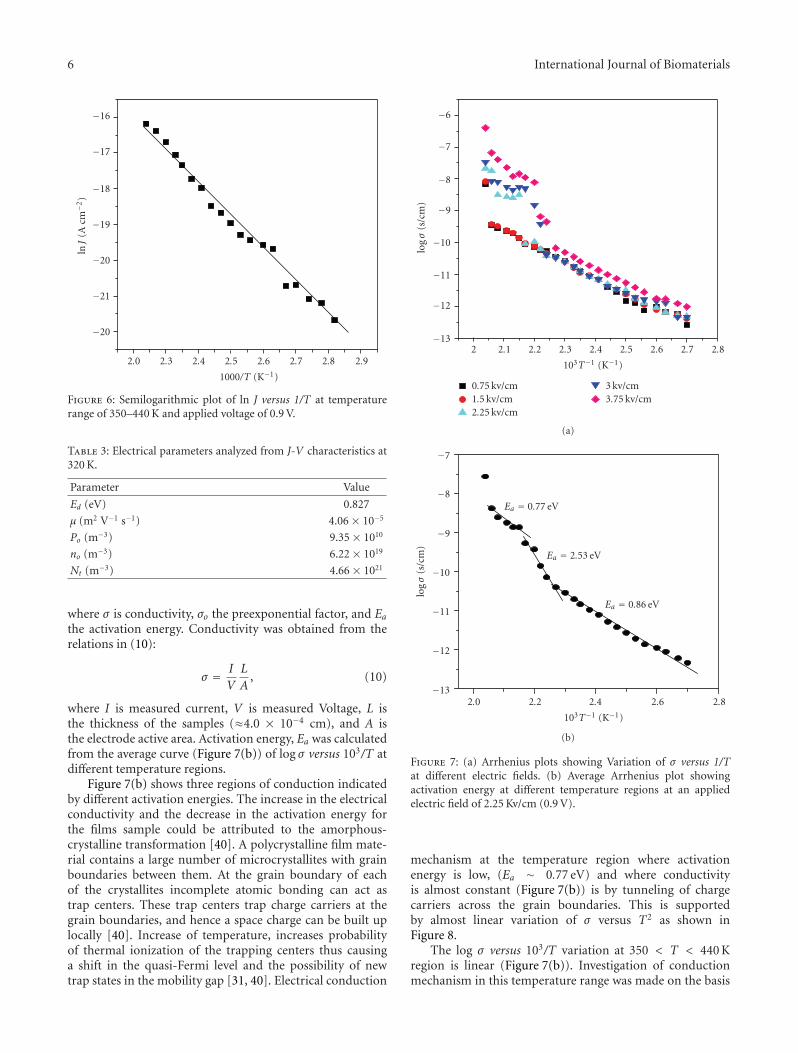
Thermal activation plots (log σ versus 103/T) for differentpolarizing fields were plotted to analyze the effect oftemperature on conductivity of the samples (Figure 7(a)).The observed dependence can be described by the Arrheniusequation (9):
σ = σ0 exp(−EakT
), (9)
6 International Journal of Biomaterials
−20
−21
−20
−19
−18
−17
−16
lnJ
(Acm
−2)
2.0 2.3 2.4 2.5 2.6 2.7 2.8 2.9
1000/T (K−1)
Figure 6: Semilogarithmic plot of ln J versus 1/T at temperaturerange of 350–440 K and applied voltage of 0.9 V.
Table 3: Electrical parameters analyzed from J-V characteristics at320 K.
Parameter Value
Ed (eV) 0.827
μ (m2 V−1 s−1) 4.06 × 10⁻⁵
Po (m−3) 9.35 × 10¹⁰
no (m−3) 6.22 × 10¹⁹
Nt (m−3) 4.66 × 10²¹
where σ is conductivity, σo the preexponential factor, and Eathe activation energy. Conductivity was obtained from therelations in (10):
σ = I
V
L
A, (10)
where I is measured current, V is measured Voltage, L isthe thickness of the samples (≈4.0 × 10⁻⁴ cm), and A isthe electrode active area. Activation energy, Ea was calculatedfrom the average curve (Figure 7(b)) of log σ versus 103/T atdifferent temperature regions.
Figure 7(b) shows three regions of conduction indicatedby different activation energies. The increase in the electricalconductivity and the decrease in the activation energy forthe films sample could be attributed to the amorphous-crystalline transformation [40]. A polycrystalline film mate-rial contains a large number of microcrystallites with grainboundaries between them. At the grain boundary of eachof the crystallites incomplete atomic bonding can act astrap centers. These trap centers trap charge carriers at thegrain boundaries, and hence a space charge can be built uplocally [40]. Increase of temperature, increases probabilityof thermal ionization of the trapping centers thus causinga shift in the quasi-Fermi level and the possibility of newtrap states in the mobility gap [31, 40]. Electrical conduction
−13
−12
−11
−10
−9
−8
−7
−6
logσ
(s/c
m)
2 2.1 2.2 2.3 2.4 2.5 2.6 2.7 2.8
103T−1 (K−1)
0.75 kv/cm1.5 kv/cm2.25 kv/cm
3 kv/cm3.75 kv/cm
(a)
−13
−12
−11
−10
−9
−8
−7
logσ
(s/c
m)
2.0 2.2 2.4 2.6 2.8
103T−1 (K−1)
Ea = 0.77 eV
Ea = 2.53 eV
Ea = 0.86 eV
(b)
Figure 7: (a) Arrhenius plots showing Variation of σ versus 1/Tat different electric fields. (b) Average Arrhenius plot showingactivation energy at different temperature regions at an appliedelectric field of 2.25 Kv/cm (0.9 V).
mechanism at the temperature region where activationenergy is low, (Ea ∼ 0.77 eV) and where conductivityis almost constant (Figure 7(b)) is by tunneling of chargecarriers across the grain boundaries. This is supportedby almost linear variation of σ versus T2 as shown inFigure 8.
The log σ versus 103/T variation at 350 < T < 440 Kregion is linear (Figure 7(b)). Investigation of conductionmechanism in this temperature range was made on the basis

International Journal of Biomaterials 7
0
0.5
1
1.5
2
2.5
3
σ(s
/cm
)×10−9
205 210 215 220 225 230
10−3T2 (K2)
Figure 8: Plot of σ versus T2 in the range 460–480 K where Ea ∼0.77 eV.
−27
−26
−25
−24
−23
−22
−21
−20
ln[σT
1/2(s
cm−1
K1/
2)]
220 224 228 232
10−3T−1/4 (K−1/4)
Figure 9: Plot of ln(σT1/2) versus (T−1/4) for NFSC within atemperature of 350 K–440 K and applied electric field of 2.25 Kv/cm.
that tunneling or hopping mechanisms can predominate.Temperature-dependence data in Figure 7(b) were reusedto plot σ versus T2, and ln(σT1/2) versus T−1/4. From thisanalysis, we noted that tunneling conduction mechanism inthe range of 350–440 K was inadequate due to nonlinearvariation of σ versus T2. Thermionic emission was also ruledout because this mechanism does not take place when theapplied voltage (V) is greater than 0.8 V [21], and at lowactivation energy [41].
Table 4: Mott parameters at temperature range of (320–440 K).
Mott parameters Value
T0 (K) 4.58 × 10¹⁰
N(EF) (eV−1cm−3) 9.04 × 10¹⁹
α (cm−1) 3.0 × 10⁸
R (cm) 1.44 × 10⁻⁷
W (eV) 0.89
Figure 9 shows linear variation of (σT1/2) versus T−1/4
thus indicating that VRH conduction process can predom-inate in this temperature range 350–450 K [41]. A good fit ofconductivity-temperature data to the expression in (11):
σT1/2 = σ0 exp
[−(T0
T
)1/4]
(11)
is necessary for applicability of VRH model. The pre-exponential factor σ0 and the degree of disorder (Motttemperature) T0 are related to the density of states N(EF),and the inverse-fall-off length of the wave function of alocalized state near the Fermi-Level α by the followingrelations [12]:
σ0 =3e3υph
(8πk)1/2
[N(EF)α
]1/2
, (12)
T0 = 18.11α3
kN(EF). (13)
To check the validity of the VRH model, ln(σT1/2) versusT−1/4 variation was plotted (Figure 9). T0, and N(EF) weredetermined from (13) using the slope in Figure 9, andassuming that α ≈ 3 A−1 which is approximately equal toinverse length of unit cell (monomer) of native cellulose[42–44]. Other Mott parameters, the distance R and averageenergy W were determined at T = 400 K by using thefollowing relations in (14) and (15) [23]:
R =[
98παkTN(EF)
]1/4
, (14)
W = 34πR3N(EF)
. (15)
The obtained Mott parameters are listed in Table 4 whichshows that the product αR and the average energy, W, satisfyMott’s requirements (αR > 1,W > kT) for variable rangehopping at this temperature range. Degree of localization ofthe carriers in the trap states indicated by αR > 1, shows thatthe charges are highly localized. Table 5 shows the variationsof the Mott parameters with temperature in our samples.It is evident from this table that αR > 1 and W > kT ,which agrees with Mott’s condition for variable range. Itcan also be noted from Table 5 that when the temperaturedecreases, the average energy W decreases and the averagedistance R increases, supporting the fact that when thephonon energy is insufficient (low temperature), carriers willtend to hop larger distances in order to locate in sites whichare energetically closer than their nearest neighbours.

8 International Journal of Biomaterials
Table 5: Variation of Mott parameters at temperature range of 300–450 K.
T (K) R (cm−1) W (eV) kT (eV) αR
300 1.54 ×10⁻⁷ 0.72 0.026 41.6
350 1.49×10⁻⁷ 0.81 0.030 40.1
400 1.44 ×10⁻⁷ 0.89 0.034 38.7
450 1.39 ×10⁻⁷ 0.98 0.039 37.6
4. Conclusion
DC conductivity measurements were performed at a tem-perature range of 320 K–450 K. Conductivity increased withtemperature. Activation energy within a wider range oftemperature was about 0.86 eV. Charge mobility analyzedfrom J-V curves was found to be 4.06 × 10⁻⁵ (m2V−1s−1).Analysis of current density-electric field dependence showedthat both Schottky and Poole-Frenkel emission cannotexplain conduction mechanism in the high fields whereSCLC was seen to be present. Plots of DC conductivity versustemperature were used to investigate Mott’s VRH conductionmodel at a temperature range of 320–440 K. This modelwas originally developed for amorphous silicon by Mott andDavis. When applied to conducting polymers, it assumesthat electron transport originates from localized or fixedstates within the polymer chain. The charge transfer betweenthe chains takes place by phononassisted hopping betweentwo localized states. Analysis of semilogarithmic plots ofln(JT1/2) versus T−1/4 gave the following Mott parameters:the degree of disorder To was in the order of 1010, thedensity of states N(EF) ≈ 1019 (eV−1cm−3) while thedistance R ≈ 10−7 cm and energy (W) were in the rangeof 0.72 eV–0.98 eV. The product αR and the average energy,W, satisfy Mott’s requirements (αR > 1, W > kT) forvariable range hopping in this temperature range. The studyhas shown that the cuticle is a promising alternative tosynthetic polymers used in electrical switching applications.Due to environmental concerns posed by nonbiodegradablesynthetic polymers, exploring this material would provideinformation on how to use it in addressing environmentalproblems and as a precursor in the design of novel materialswith electrical functionality such as the modern nonvolatilememory chips, biosensors, and biological transistors.
Acknowledgments
The authors wish to thank Professor F. Kremer, the directorof Institute of Experimental Physics I at Leipzig University(Germany) for availing AFM instruments. A useful dis-cussion with Dr. Periklis Papadopolous concerning FTIRmeasurements is gratefully acknowledged.
References
[1] J. J. Davis, “Molecular bioelectronics,” Philosophical Transac-tions of the Royal Society A, vol. 361, no. 1813, pp. 2807–2825,2003.
[2] J. J. Benıtez, R. Garcıa-Segura, and A. Heredia, “Plantbiopolyester cutin: a tough way to its chemical synthesis,”Biochimica et Biophysica Acta, vol. 1674, no. 1, pp. 1–3, 2004.
[3] W. K. Kipnusu, G. Katana, C. M. Migwi, I. V. S. Rathore,and J. R. Sangoro, “Electrical switching in Nandi flame seedcuticle biopolymer thin films,” International Journal of PolymerScience, vol. 2009, Article ID 830270, 10 pages, 2009.
[4] A. Tiwari and S. P. Singh, “Synthesis and characterizationof biopolymer-based electrical conducting graft copolymers,”Journal of Applied Polymer Science, vol. 108, no. 2, pp. 1169–1177, 2008.
[5] A. Tiwari, “Synthesis and characterization of pH switchingelectrical conducting biopolymer hybrids for sensor applica-tions,” Journal of Polymer Research, vol. 15, no. 4, pp. 337–342,2008.
[6] A. Tiwari and V. Singh, “Synthesis and characterizationof electrical conducting chitosan-graft-polyaniline,” eXPRESSPolymer Letters, vol. 1, no. 5, pp. 308–317, 2007.
[7] H. Peng, L. Zhang, C. Soeller, and J. Travas-Sejdic, “Conduct-ing polymers for electrochemical DNA sensing,” Biomaterials,vol. 30, no. 11, pp. 2132–2148, 2009.
[8] M. H. Buraidah, L. P. Teo, S. R. Majid, and A. K. Arof, “Ionicconductivity by correlated barrier hopping in NH4I dopedchitosan solid electrolyte,” Physica B, vol. 404, no. 8-11, pp.1373–1379, 2009.
[9] S. S. Pradhan and A. Sarkar, “Enhancement of electricalconductivity in the Gum Arabica complex,” Materials Scienceand Engineering C, vol. 29, no. 6, pp. 1790–1793, 2009.
[10] C. J. Bettinger, J. P. Bruggeman, A. Misra, J. T. Borenstein, andR. Langer, “Biocompatibility of biodegradable semiconduct-ing melanin films for nerve tissue engineering,” Biomaterials,vol. 30, no. 17, pp. 3050–3057, 2009.
[11] K. D. Meisel, W. F. Pasveer, J. Cottaar, et al., “Charge-carriermobilities in disordered semiconducting polymers: effects ofcarrier density and electric field,” Physica Status Solidi C, vol.3, no. 2, pp. 267–270, 2006.
[12] N. Mott and E. Davis, Electronic Processes in Non-CrystallineMaterials, Clarendon, Oxford, UK, 2nd edition, 1979.
[13] M. Ghosh, A. K. Meikap, S. K. Chattopadhyay, and S. Chat-terjee, “Low temperature transport properties of Cl-dopedconducting polyaniline,” Journal of Physics and Chemistry ofSolids, vol. 62, no. 3, pp. 475–484, 2001.
[14] V. Luthra, R. Singh, S. K. Gupta, and A. Mansingh, “Mech-anism of dc conduction in polyaniline doped with sulfuricacid,” Current Applied Physics, vol. 3, no. 2-3, pp. 219–222,2003.
[15] R. Singh, A. Kaur, K. Lal Yadav, and D. Bhattacharya,“Mechanism of dc conduction in ferric chloride doped poly(3-methyl thiophene),” Current Applied Physics, vol. 3, no. 2-3,pp. 235–238, 2003.
[16] Z. G. Yu and X. Song, “Variable range hopping and electricalconductivity along the DNA double helix,” Physical ReviewLetters, vol. 86, no. 26 I, pp. 6018–6021, 2001.
[17] A. Tiwari, V. Sen, S. R. Dhakate, A. P. Mishra, and V. Singh,“Synthesis, characterization, and hoping transport propertiesof HCl doped conducting biopolymer-co-polyaniline zwitte-rion hybrids,” Polymers for Advanced Technologies, vol. 19, no.7, pp. 909–914, 2008.
[18] M. V. Garcia-Cuenca, J. L. Morenza, and J. Esteve, “Electrontunneling in heavily in-doped polycrystalline CdS films,”Journal of Applied Physics, vol. 56, no. 6, pp. 1738–1743, 1984.
[19] A. A. El Tayyan and A. Khogali, “DC conduction inFe3+ poly(9-vinylcarbazole) doped films,” Chinese Journal ofPhysics, vol. 42, no. 4 I, pp. 392–400, 2004.

International Journal of Biomaterials 9
[20] S. H. Deshmukh, D. K. Burghate, V. P. Akhare, V. S.Deogaonkar, P. T. Deshmukh, and M. S. Deshmukh, “Electri-cal conductivity of polyaniline doped PVC-PMMA polymerblends,” Bulletin of Materials Science, vol. 30, no. 1, pp. 51–56,2007.
[21] A. Aziz, Y. Khlifi, K. Kassmi, and F. Olivie, “Modellingof conduction properties of Schottky diodes in polymers,”Condensed Matter, vol. 8, pp. 21–32, 2007.
[22] F. Gmati, A. Fattoum, N. Bohli, W. Dhaoui, and A. B.Mohamed, “Comparative studies of the structure, morphol-ogy and electrical conductivity of polyaniline weakly dopedwith chlorocarboxylic acids,” Journal of Physics: CondensedMatter, vol. 19, no. 32, Article ID 326203, 2007.
[23] T. G. Abdel-Malik, R. M. Abdel-Latif, A. Sawaby, and S. M.Ahmed, “Electrical properties of pure and doped polyvinylalcohol (PVA) films using gold and aluminum electrodes,”Journal of Applied Sciences Research, vol. 4, no. 3, pp. 331–336,2008.
[24] N. P. Armitage, M. Briman, and G. Gruner, “Charge transferand charge transport on the double helix,” Physica Status SolidiB, vol. 1, no. 1, pp. 69–75, 2004.
[25] L. Tao, A. Erfan, and K. Heinz-Bernhard, “Peptide electrontransfer,” Chemistry: A European Journal, vol. 11, pp. 5186–5194, 2005.
[26] P. Ronald, R. Peter, and S. Albert, “Water structure-dependence charge transport in protein,” Proceedings of theNational Academy of Sciences of the United States of America,vol. 78, no. 1, pp. 261–265, 1981.
[27] B. Radha and D. Rossen, “Nonlinear elastodynamics andenergy transport in biopolymers,” http://arxiv.org/abs/nlin/0304060.
[28] L. Chopra, Thin Film Phenomena, McGraw-Hill, New York,NY, USA, 1969.
[29] R. H. Wilson, A. C. Smith, M. Kacurakova, P. K. Saunders, N.Wellner, and K. W. Waldron, “The mechanical properties andmolecular dynamics of plant cell wall polysaccharides studiedby Fourier-transform infrared spectroscopy,” Plant Physiology,vol. 124, no. 1, pp. 397–405, 2000.
[30] A. A. Baker, W. Helbert, J. Sugiyama, and M. J. Miles, “Newinsight into cellulose structure by atomic force microscopyshows the Iα crystal phase at near-atomic resolution,” Biophys-ical Journal, vol. 79, no. 2, pp. 1139–1145, 2000.
[31] P. K. Khare, R. K. Pandey, and P. L. Jain, “Electrical transport inethyl cellulose-chloranil system,” Bulletin of Materials Science,vol. 23, no. 4, pp. 325–330, 2000.
[32] R. Parthasarathy, X.-M. Lin, K. Elteto, T. F. Rosenbaum,and H. M. Jaeger, “Percolating through networks of randomthresholds: finite temperature electron tunneling in metalnanocrystal arrays,” Physical Review Letters, vol. 92, no. 7,Article ID 076801, 4 pages, 2004.
[33] L. Pendar and R. Flening, “Memory switching in glowdischarge polymerised thin Films,” Journal of Applied Physics,vol. 46, pp. 3426–3431, 1975.
[34] D. Ottenbacher, K. D. Schierbaum, and W. Goepel, “Switchingeffects in metal/phthalocyanine/metal sandwich structures,”Journal of Molecular Electronics, vol. 7, no. 2, pp. 79–84, 1991.
[35] Z. Q. Xue, M. Ouyang, K. Z. Wang, H. X. Zhang, and C. H.Huang, “Electrical switching and memory phenomena in theAg-BDCP thin film,” Thin Solid Films, vol. 288, no. 1-2, pp.296–299, 1996.
[36] G. Katana and A. Musyoki, “Fabrication and performancetesting of gas sensors based on organic thin films,” Journal ofPolymer Materials, vol. 24, no. 4, pp. 387–394, 2007.
[37] D. Savransky, “Model of conductivity transition in amorphouschalcogenides induced by auger recombination,” Journal ofOvonic Research, vol. 1, no. 2, pp. 25–30, 2005.
[38] M. M. Akhmedov, M. K. Kerimov, B. A. Suleimanov, and S. A.Mansimov, “Space charge limited current in films obtained inglow discharge plasma,” Turkish Journal of Physics, vol. 22, no.3, pp. 253–261, 1998.
[39] G. D. Sharma, S. G. Sangodkar, and M. S. Roy, “Study onelectrical and photoelectrical behaviour of thin films of allylviologen (AV) in PVA matrix,” Journal of Materials Science:Materials in Electronics, vol. 8, no. 1, pp. 47–55, 1997.
[40] E. M. Farag and M. M. Sallam, “Composition dependence ofthe grain size, activation energy and coordination number inGe40−xInxSe60(10 ≤ x ≤ 40at.%) thin films,” Egyptian Journalof Solids, vol. 30, no. 1, pp. 1–11, 2007.
[41] I. Gunal and M. Parlak, “Current transport mechanisms in lowresistive CdS thin films,” Journal of Materials Science: Materialsin Electronics, vol. 8, no. 1, pp. 9–13, 1997.
[42] K. Gessler, N. Krauss, T. Steiner, C. Betzel, A. Sarko, and W.Saenger, “β-D-cellotetraose hemihydrate as a structural modelfor cellulose II. An X-ray diffraction study,” Journal of theAmerican Chemical Society, vol. 117, no. 46, pp. 11397–11406,1995.
[43] M. Wada, J. Sugiyama, and T. Okano, “Native celluloses onthe basis of two crystalline phase (Iα/Iβ) system,” Journal ofApplied Polymer Science, vol. 49, no. 8, pp. 1491–1496, 1993.
[44] F. J. Kolpak and J. Blackwell, “Determination of the structureof cellulose II,” Macromolecules, vol. 9, no. 2, pp. 273–278,1976.

Submit your manuscripts athttp://www.hindawi.com
ScientificaHindawi Publishing Corporationhttp://www.hindawi.com Volume 2014
CorrosionInternational Journal of
Hindawi Publishing Corporationhttp://www.hindawi.com Volume 2014
Polymer ScienceInternational Journal of
Hindawi Publishing Corporationhttp://www.hindawi.com Volume 2014
Hindawi Publishing Corporationhttp://www.hindawi.com Volume 2014
CeramicsJournal of
Hindawi Publishing Corporationhttp://www.hindawi.com Volume 2014
CompositesJournal of
NanoparticlesJournal of
Hindawi Publishing Corporationhttp://www.hindawi.com Volume 2014
Hindawi Publishing Corporationhttp://www.hindawi.com Volume 2014
International Journal of
Biomaterials
Hindawi Publishing Corporationhttp://www.hindawi.com Volume 2014
NanoscienceJournal of
TextilesHindawi Publishing Corporation http://www.hindawi.com Volume 2014
Journal of
NanotechnologyHindawi Publishing Corporationhttp://www.hindawi.com Volume 2014
Journal of
CrystallographyJournal of
Hindawi Publishing Corporationhttp://www.hindawi.com Volume 2014
The Scientific World JournalHindawi Publishing Corporation http://www.hindawi.com Volume 2014
Hindawi Publishing Corporationhttp://www.hindawi.com Volume 2014
CoatingsJournal of
Advances in
Materials Science and EngineeringHindawi Publishing Corporationhttp://www.hindawi.com Volume 2014
Smart Materials Research
Hindawi Publishing Corporationhttp://www.hindawi.com Volume 2014
Hindawi Publishing Corporationhttp://www.hindawi.com Volume 2014
MetallurgyJournal of
Hindawi Publishing Corporationhttp://www.hindawi.com Volume 2014
BioMed Research International
MaterialsJournal of
Hindawi Publishing Corporationhttp://www.hindawi.com Volume 2014
Nano
materials
Hindawi Publishing Corporationhttp://www.hindawi.com Volume 2014
Journal ofNanomaterials