charge and ion dynamics in light-emitting electrochemical ... · pdf filecharge and ion...
TRANSCRIPT

Charge and ion dynamics in light-emittingelectrochemical cells : understanding the operationalmechanism from electrical transport to light generationvan Reenen, S.
DOI:10.6100/IR776754
Published: 01/01/2014
Document VersionPublisher’s PDF, also known as Version of Record (includes final page, issue and volume numbers)
Please check the document version of this publication:
• A submitted manuscript is the author's version of the article upon submission and before peer-review. There can be important differencesbetween the submitted version and the official published version of record. People interested in the research are advised to contact theauthor for the final version of the publication, or visit the DOI to the publisher's website.• The final author version and the galley proof are versions of the publication after peer review.• The final published version features the final layout of the paper including the volume, issue and page numbers.
Link to publication
Citation for published version (APA):Reenen, van, S. (2014). Charge and ion dynamics in light-emitting electrochemical cells : understanding theoperational mechanism from electrical transport to light generation Eindhoven: Technische UniversiteitEindhoven DOI: 10.6100/IR776754
General rightsCopyright and moral rights for the publications made accessible in the public portal are retained by the authors and/or other copyright ownersand it is a condition of accessing publications that users recognise and abide by the legal requirements associated with these rights.
• Users may download and print one copy of any publication from the public portal for the purpose of private study or research. • You may not further distribute the material or use it for any profit-making activity or commercial gain • You may freely distribute the URL identifying the publication in the public portal ?
Take down policyIf you believe that this document breaches copyright please contact us providing details, and we will remove access to the work immediatelyand investigate your claim.
Download date: 10. May. 2018

Chargeandiondynamicsinlight‐emittingelectrochemicalcells
Understandingtheoperationalmechanismfromelectricaltransporttolightgeneration
PROEFSCHRIFT
ter verkrijging van de graad van doctor aan de Technische Universiteit Eindhoven, op gezag van de rector magnificus prof.dr.ir. C.J. van Duijn, voor
een commissie aangewezen door het College voor Promoties, in het openbaar te verdedigen
op dinsdag 23 september 2014 om 16:00 uur
door
Stephan van Reenen
geboren te Eindhoven

Dit proefschrift is goedgekeurd door de promotoren en de samenstelling van de
promotiecommissie is als volgt:
voorzitter: prof.dr.ir. G.M.W. Kroesen
1e promotor: prof.dr.ir. M. Kemerink
2e promotor: prof.dr.ir. R.A.J. Janssen
leden: prof.dr. L. Edman (Umeå University)
prof.dr.ir. P.W.M. Blom (Max Plank Institute for
Polymer Research, Mainz)
prof.dr. R. Coehoorn (Philips Research & Eindhoven
University of Technology)
prof.dr. B. Koopmans
adviseur: dr. H.J. Bolink (Universidad de Valencia)


A catalogue record is available from the Eindhoven University of Technology Library
ISBN: 978‐90‐386‐3667‐2
Printed by Universiteitsdrukkerij Technische Universiteit Eindhoven
This thesis is part of NanoNextNL, a micro and nanotechnology innovation programme of
the Dutch Government and 130 partners from academia and industry. More information
on www.nanonextnl.nl

Contents
Contents .................................................................................................................... 221
Chapter 1 Low‐cost lighting by light‐emitting electrochemical cells ............................ 5 1.1 Low‐cost lighting from organic semiconductors .......................................................... 6 1.2 Organic light‐emitting electrochemical cells ............................................................... 7 1.3 Aim and outline of thesis ........................................................................................... 11
Chapter 2 A unifying model for the operation of polymer LECs ................................ 17 2.1 Introduction ............................................................................................................... 18 2.2 Material and methods ............................................................................................... 19 2.3 Results and discussion ............................................................................................... 21 2.4 Conclusions ................................................................................................................ 27
Chapter 3 Salt concentration effects ........................................................................ 31 3.1 Introduction ............................................................................................................... 32 3.2 Material and methods ............................................................................................... 33 3.3 Results and discussion ............................................................................................... 34 3.4 Conclusions ................................................................................................................ 44
Chapter 4 Doping dynamics in light‐emitting electrochemical cells .......................... 47 4.1 Introduction ............................................................................................................... 48 4.2 Material and methods ............................................................................................... 49 4.3 Results and discussion ............................................................................................... 50 4.4 Conclusions ................................................................................................................ 59 4.5 Supplemental figures ................................................................................................. 60
Chapter 5 Dynamic processes in stacked polymer LECs ............................................ 65 5.1 Introduction ............................................................................................................... 66 5.2 Material and methods ............................................................................................... 67 5.3 Results and discussion ............................................................................................... 68 5.4 Conclusions ................................................................................................................ 80
Chapter 6 Dynamic doping in planar iTMC‐LECs ....................................................... 83 6.1 Introduction ............................................................................................................... 84 6.2 Material and methods ............................................................................................... 84 6.3 Results and discussion ............................................................................................... 86 6.4 Conclusions ................................................................................................................ 95
Chapter 7 Universal transients in polymer‐ and iTMC‐LECs....................................... 97 7.1 Introduction ............................................................................................................... 98 7.2 Material and methods ............................................................................................... 98 7.3 Results and discussion ............................................................................................. 100 7.4 Conclusions .............................................................................................................. 106
Chapter 8 Photoluminescence quenching by electrochemical doping ..................... 109 8.1 Introduction ............................................................................................................. 110 8.2 Materials and methods ............................................................................................ 110 8.3 Experimental results ................................................................................................ 111 8.4 Discussion ................................................................................................................ 117 8.5 Conclusions .............................................................................................................. 126

8.6 Supplemental figures ............................................................................................... 126
Chapter 9 Understanding the efficiency in LECs ..................................................... 131 9.1 Introduction ............................................................................................................. 132 9.2 Materials and methods ............................................................................................ 133 9.3 Results and discussion ............................................................................................. 135 9.4 Conclusions .............................................................................................................. 144
Chapter 10 Large magnetic field effects in electrochemically doped polymer LECs ... 147 10.1 Introduction ........................................................................................................... 148 10.2 Materials and methods .......................................................................................... 148 10.3 Experimental results .............................................................................................. 150 10.4 Discussion .............................................................................................................. 152 10.5 Conclusions ............................................................................................................ 165
Chapter 11 Origin of work function modification by electrolytes ............................. 169 11.1 Introduction ........................................................................................................... 170 11.2 Materials and methods .......................................................................................... 172 11.3 Results and discussion ........................................................................................... 174 11.4 General considerations .......................................................................................... 186 11.5 Conclusion .............................................................................................................. 186
Chapter 12 Perspective on the future of LECs .......................................................... 191 12.1 Current view on operational mechanism of LECs .................................................. 192 12.2 Future directions to improve LECs ......................................................................... 194
Appendix ................................................................................................................... 199 A Numerical model to describe operation of LECs ........................................................ 200
Summary ................................................................................................................... 211
Samenvatting ............................................................................................................ 217
About the author ....................................................................................................... 227
List of publications ..................................................................................................... 229
Dankwoord ................................................................................................................ 231

Chapter1 Low‐costlightingbylight‐
emittingelectrochemicalcells
Light‐emitting electrochemical cells (LECs) are potential candidates for next‐generation,
low‐cost, large‐area lighting applications. LECs consist of a single, solution‐processed
active layer which consists of an organic semiconductor admixed with mobile ions. Its
merits are excellent processing characteristics without a large compromise in performance.
Understanding of the fundamental device operation of LECs is however limited. This thesis
aims to understand the transient and steady‐state operation of LECs by investigating
electronic carrier injection, transport and recombination in the presence of mobile ions.
This understanding is utilized to assess the limits in device performance and to determine
routes for optimization.

6 Chapter 1 | Low‐cost lighting by light‐emitting electrochemical cells
1.1 Low‐costlightingfromorganicsemiconductorsArtificial lighting is a crucial part of everyday life, providing illumination in absence of
sufficient daylight or to convey information by displays. The aesthetic function of lighting
is becoming increasingly important as well. These functions add up to a large global
market, which requires durable and energy efficient lighting technologies. The fastest
growing and promising lighting technologies at this moment are based on inorganic and
organic semiconductors. State‐of‐the‐art lighting from inorganic semiconductors already
outperforms older technologies like incandescent and fluorescent lighting in efficiency,
while development of lighting from organic semiconductors is still in progress.1‐2 Inorganic
light emitting diodes (LEDs) are already widely used in televisions, lamps, and signage
applications. Also organic light emitting diodes (OLEDs) have recently hit the market and
are mainly employed as decorative lighting sources and in displays.
OLEDs promise revolutionary properties like transparency, color tunability and flexibility
while being low‐cost. Opposed to LEDs, OLEDs have a superior response time, viewing
angle, contrast ratio, and color rendering index, while being less thick and heavy.
However, lifetime, efficiency, cost, and resolution are so far mainly in favor of LEDs.
Figure 1.1 (a) Schematic device layout of a single‐layer OLED. (b) Schematic of the conversion of electricity in light with subsequently charge injection (black arrows), transport (gray arrows), and recombination (white arrows).
In its most basic form, an OLED consists of two electrodes which sandwich a thin
semiconducting film as shown in Figure 1.1a. This film consists of either a polymer or small
molecule semiconductor. One of the advantages of organic semiconductors is that they
can be deposited from solution.3‐7 This makes OLEDs promising for low‐cost production
like printing in a roll‐to‐roll process. Next to low production costs, also a sufficient
efficiency is required to compete with inorganic lighting technologies. For an efficient
device the conversion of electrical energy into light needs to be optimized. In (O)LEDs this
conversion follows the chain carrier injection, transport, and recombination as shown in
Figure 1.1b. Optimization of all these processes in one and the same material is not at all

Charge and ion dynamics in light‐emitting electrochemical cells 7
straight‐forward as e.g. improvement of transport by modification of the material may
lead to a reduction in recombination efficiency. In addition, optoelectronic processes in
solution‐processed OLEDs can suffer from contaminations which are introduced during
the fabrication by solvents or the atmosphere.8 Batch‐to‐batch variation in polymers is
also known to lead to irreproducibility.
Figure 1.2 (a) Schematic device layout of a multilayer OLED. (b) Schematic of the conversion of electricity in light with subsequently charge injection (black arrows), transport (gray arrows), and recombination (white arrows).
Rather than optimizing a single layer, multilayer stacks as shown in Figure 1.2a can be
used. In efficient OLEDs, the different functionalities related to injection, transport,
recombination and blocking of charge carriers are distributed over multiple layers (see
Figure 1.2b) so each layer needs only to be optimized for a limited number of
functionalities. The fabrication of such a device is however more challenging compared to
the single layered device shown in Figure 1.1a. The fabrication of multilayer OLEDs from
solution, see e.g. Ref. 9, is challenging as dissolution of previous layers must be avoided.
Therefore multilayer OLEDs are typically deposited in vacuum by thermal evaporation of
small organic molecules. Besides the ability to fabricate multilayer OLEDs, other
advantages of thermal evaporation in vacuum are good control over the layer thickness
and the avoidance of contaminations in the bulk and at the interfaces. This is part of the
reason that the highest efficiencies in OLEDs reported to date are obtained in vacuum
evaporated small molecule OLEDs. This type of OLEDs is already commercially available.
The cost of these devices is however relatively high compared to competing and more
mature technologies like LEDs. A lowering of the price is still expected as costs will scale
with the production volume. However, to make lighting from organics compete with e.g.
LEDs, more innovation is required.
1.2 Organiclight‐emittingelectrochemicalcellsLight‐emitting electrochemical cells (LECs) promise a combination of the advantages in
performance of multilayer OLEDs and the advantages in processability of single‐layered

8 Chapter 1 | Low‐cost lighting by light‐emitting electrochemical cells
OLEDs. LECs consist of a single medium which allows the simultaneous transport of
anions/cations and electrons/holes. When a bias voltage is applied to turn the device on,
the ions redistribute in such a way that different regions are created within the single
layer as shown in Figure 1.3. These different regions take subsequently care of carrier
injection, transport and recombination. Opposed to the many layers typically encountered
in vacuum deposited OLEDs, the single, solution‐processable layer in LECs furthermore
allows facile, cheap, large‐scale production techniques like printing. Roll‐to‐roll deposition
of LECs was for example recently demonstrated by Edman et al.10
Figure 1.3 (a) Schematic device layout of an LEC, consisting of a single material which upon biasing has in‐situ formed multiple layers. (b) Schematic of the conversion of electricity in light with subsequently charge injection (black arrows), transport (gray arrows), and recombination (white arrows).
LECs can be operated efficiently in forward and reverse bias,11 which indicates that the
electrode material is not so crucial for efficient carrier injection, unlike in standard OLEDs
(as shown in Figure 1.1). This allows the use of cheap and/or air‐stable electrode
materials. Furthermore LECs boast efficient carrier transport properties highlighted by
efficient operation with an active layer thickness between 10‐7 m and 10‐6 m.10, 12‐13
Devices with a thickness of 10‐3 m moreover still generate light that is detectable by
eye.14‐15 This weak relation between efficiency and active layer thickness provides a
relatively large tolerance for large scale production of LECs, which is favorable for the final
costs. For comparison, in OLEDs small tolerances of 10‐9 m in layer thicknesses are
required.
The question which remains is at which price the above advantages of LECs come.
Currently, LECs have a slow response time above a millisecond.16‐17 Although this is
substantial, the technology is still sufficient for applications like signage or ambient
lighting. The peak efficiency of white LECs currently lies around 20 lm W‐1.18‐19 To give an
indication of the currently reached lifetimes, the LECs reported in Ref. 16 can run over
4000 h before their luminance is reduced to half the initial luminance of 670 cd m‐2.

Charge and ion dynamics in light‐emitting electrochemical cells 9
Solution‐processed OLEDs achieve similar efficiencies20 but still require multiple layers
with well‐defined thicknesses.4‐6 In Table 1.1 an overview is given of the highest reported
brightness, efficiency and lifetime in white lighting technologies based on small molecule
OLEDs, solution‐processed OLEDs and LECs (small molecule and polymer).
Table 1.1 Performance of organic white lighting technologies Technology Brightness (cd m-2) Efficiency (%; lm W-1; cd A-1) Lifetime (hours)
Small molecule LECs 115 (at 4 V) 21 11; 20; 20 18-19 24000 (at 100 cd m-2) 16
Polymer LECs 6240 (at 9.5 V) 22 2.4 23; 1.2; 3.8 22 6000 (at 100 cd m-2) 22
Solution-processed OLEDs 30000 (at 9 V) 24 28.8; 40 ; 60 25 1000 (at 100 cd m-2) 26
Small molecule OLEDs 48000 (at 12 V) 27 50 28; 139 29; - 100000 (at 1000 cd m-2) 30
The active layer of LECs basically consists of a semiconducting as well as ionically
conductive material. In literature mainly two types of LECs can be distinguished, either
based on semiconducting polymers mixed with ions, or based on semiconducting small
molecules which are ionic by themselves. In the next paragraphs both types are discussed
in more detail.
1.2.1 PolymersemiconductorsPolymer LECs were first introduced by Pei et al.11 and typically consist of a semiconducting
polymer blended with a solid electrolyte, e.g. poly(ethylene oxide) (PEO) admixed with
potassium triflate (KTf or KCF3SO3) (see Figure 1.4).31 In these devices the semiconductor
facilitates transport of electronic carriers, whereas ionic carrier transport is facilitated by
the PEO. Phase separation of the different components must be prevented and therefore
must be taken into account in the choice of material. In general some poly(p‐phenylene
vinylene) (PPV) derivatives (see e.g. Figure 1.4) are found to mix well with the typically
used PEO.
Figure 1.4 Structural formulae for typical constituents of polymer LECs.
The PPV derivatives used for the work in this thesis are poly[2‐methoxy‐5‐(3’,7’‐
dimethyloctyloxy)‐p‐phenylene vinylene] (MDMO‐PPV, American Dye Source) and a
phenyl‐substituted poly(p‐phenylene vinylene) copolymer (SY‐PPV, Merck, catalogue
number PDY‐132), commonly termed “Super Yellow”. The oxidation and reduction levels
of PPV and PEO furthermore favor injection of electronic charge carriers in PPV over
MDMO‐PPV PEO K+Tf‐SY‐PPV

10 Chapter 1 | Low‐cost lighting by light‐emitting electrochemical cells
injection in PEO, preventing undesired oxidation or reduction of the PEO.32 In addition, p‐
and n‐type transport in PPV is relatively balanced.33 Alternatives for the electrolyte are
ionic liquids like methyltrioctylammonium trifluoromethanesulfonate (MATS).34
1.2.2 SmallmoleculesemiconductorsA year after the first report on polymer LECs another type of LEC, based on small
molecules, was introduced.35‐37 These small molecules are semiconducting transition
metal complexes which are intrinsically ionic. When used as active layer in LECs such an
ionic transition metal complex (iTMC) takes care of both ionic and electronic transport. An
example of an iTMC is the cationic iridium complex bis(2‐phenylpyridine‐C,N)(2,2'‐
bipyridine‐N,N')iridium(III) hexafluorophosphate [Ir(ppy)2(bpy)]+ (PF6
−) shown in Figure
1.5.38 Variation in iTMCs are possible by modification of the ligands or the central metal
atom. Complexes based on ruthenium39 or copper40 have also been reported but are not
as stable and efficient as iridium‐based iTMCs.37 The advantage of Ir‐iTMC‐LECs compared
to polymer LECs is that the Ir‐iTMCs are triplet emitters, resulting in a larger radiative
recombination efficiency after exciton formation. The response time of LECs based on Ir‐
iTMCs is however very low, i.e. several hours,38 but can be enhanced by admixing with
PEO, as has been shown for Ru‐based iTMCs in Ref. 41, or an ionic liquid like 1‐butyl‐3‐
methylimidazolium hexafluorophosphate (BMIM+PF6‐) to a turn‐on time of a few
minutes.38 Use of a constant current driving approach can even reduce the turn‐on time to
roughly 10‐5 s.16 iTMCs dissolve in benign solvents allowing for environmentally friendly
processing. Another benefit is the ease of color tunability in iridium(III) ionic transition
metal complexes (Ir‐iTMCs) which enables a color range covering the entire visible
spectrum, including white.18, 21, 37, 42‐45
Figure 1.5 Structural formulae for typical constituents of ionic transition metal complex (iTMC) LECs.
[Ir(ppy)2(bpy)]+PF6
‐ BMIM+PF6‐
Charge and ion dynamics in light‐emitting electrochemical cells 11
1.3 AimandoutlineofthesisAlthough LECs offer promising features regarding processing and performance, significant
research is still required to assess their limits and to maximize their performance.
Fundamental and quantitative understanding of the LEC device operation are crucial to
address loss processes affecting the performance and to give direction to materials
synthesis. The aim of this thesis is to conceptually and quantitatively understand the
dominant processes in LEC operation. The full line of events from carrier injection,
doping/ion dynamics, charge transport until the (non‐)radiative recombination processes
is therefore investigated in LECs based on polymer and iTMC semiconductors. Both the
turn‐on and steady‐state operation will be addressed. Moreover the potential and limits
of LEC devices in their current form are assessed in terms of performance. An outline of
the thesis is given below.
For a decade the device operation of LECs was described by two competing models, the
electrochemical doping model and the electrodynamic model. In Chapter 2 experimental,
numerical and analytical methods are combined on planar (10‐4 m interelectrode gap)
polymer LECs to establish a universal model for the operation of LECs. The model unifies
both previous models. The electrochemical doping model is found to describe the
operation of optimized LECs, whereas the electrodynamic model arises in case charge
injection is limited. According to the electrochemical doping model, a light‐emitting p‐i‐n
junction forms in between electrochemically doped p‐ and n‐type regions. Chapter 2 also
serves as a more specific introduction to the (processes involved in the) operation of LECs.
In Chapter 3 the effects of ion density on the device operation is studied in planar polymer
LECs. A large ion density is found to enhance carrier injection and transport by increased
electrochemical doping. To optimize LECs for charge transport, while ignoring the effects
of doping on the radiative efficiency, an as high as possible ion density is found to be
preferred, provided electronic carrier injection can follow the enhanced bulk conductivity.
In Chapter 4 the dynamics of electrochemical doping in planar polymer LECs is
investigated. During turn‐on doping fronts are observed to sweep through the device
towards each other, subsequently forming a light‐emitting p‐i‐n junction. Numerical drift
diffusion modeling proves that such doping fronts arise from the combination of a strong
doping dependence in the electronic carrier mobility and an ion mobility which is
comparable to the undoped electronic carrier mobility. These results give insight in the
origin of the turn‐on time in LECs.
In order to generalize the results obtained on planar cells in previous chapters, Chapter 5
investigates the operational behavior of stacked (10‐7 m interelectrode gap) polymer
LECs by impedance spectroscopy. Steady‐state characteristics observed in planar cells are

12 Chapter 1 | Low‐cost lighting by light‐emitting electrochemical cells
found to be also present in stacked cells: electric double layers improving carrier injection
and electrochemical doping leading to the formation of a light‐emitting p‐i‐n junction. In
addition, the long turn‐on time typical for LECs is found to be limited by salt dissociation
into ions rather than by ion migration.
In Chapter 6 the operation of iTMC‐LECs is investigated in planar cell configuration (10‐5 m interelectrode gap). Scanning Kelvin probe microscopy and UV excited
photoluminescence experiments show that reversible electrochemical doping takes place
in this type of materials. A dynamic light‐emitting p‐i‐n junction is observed away from the
contacts which proves without doubt that the electrochemical doping model not only
applies to polymer LECs, but also iTMC‐LECs.
In Chapter 7 the temperature dependent transient behavior of the current, luminance and
efficacy of stacked iTMC and polymer LECs are studied and compared. These results show
highly similar transient behavior in both types of LECs. This demonstrates that no
fundamental difference exists between charge transport and quenching processes in small
molecule and mixed polymeric active materials.
Attention is then switched from charge transport to the conversion of electronic carriers
in photons in Chapter 8. Here exciton quenching in electrochemically doped polymer
semiconductors is studied. Photoluminescence quenching is observed to arise at carrier
densities between 1018 and 1019 cm‐3. The doping dependence of the PL quenching can be
described by Förster resonance energy transfer and by charge transfer, both between
diffusing excitons and ion‐compensated polarons.
The quenching relations found in the previous chapter are used in Chapter 9 to describe
experimental results which evidence quenching by electrochemical doping. Enhancing the
admixed salt density was found to lead to reduced luminescent efficiency. Numerical
modeling, including doping‐induced exciton quenching (Chapter 8), was successfully used
to model the experiments qualitatively and quasi‐quantitatively. This shows that all the
major processes describing operational PPV‐based LECs are known and taken into account
in the model, highlighting the current understanding of LEC operation. The relatively low
efficiency in LECs, compared to OLEDs, is found to be intrinsically related to the use of
dopants to improve charge transport.
In Chapter 10 magnetic field effects in an electrochemically doped polymer LEC are
studied. Large magneto‐resistance is observed simultaneous with positive magneto‐
electroluminescence. These effects are related to competition between spin mixing and
exciton formation leading to an enhanced singlet:triplet ratio at nonzero magnetic field.
The resultant reduction in triplet exciton density is argued to reduce detrapping of
polarons in the recombination zone at low bias voltages, explaining the observed

Charge and ion dynamics in light‐emitting electrochemical cells 13
magneto‐resistance. At high electric fields a negative magneto‐electroluminescence effect
is observed which is rationalized by triplet‐triplet annihilation that leads to delayed
fluorescence. In the studied devices delayed fluorescence enhances the efficiency of
singlet emitter‐based (polymer) LECs by at most 17 %.
Thin ionic interface layers have been reported to modify electrode work functions,
improving electronic carrier injection into organic electronic devices. To determine
whether LEC‐type ion‐induced doping is the underlying mechanism, such interface layers
are studied in Chapter 11. Conversely, work function modification is found to originate
from interfacial dipole formation, induced by image charges in the contacting material.
Asymmetry in the ionic constituents, i.e. in size and ability to approach the interface, is
shown to lead to the formation of a net dipole for a wide range of materials.

14 Chapter 1 | Low‐cost lighting by light‐emitting electrochemical cells
References
[1] S. Reineke, M. Thomschke, B. Lussem, K. Leo, Rev. Mod. Phys. 85 (2013) 1245.
[2] Y. Narukawa, M. Sano, T. Sakamoto, T. Yamada, T. Mukai, Phys. Status Solidi A 205 (2008) 1081.
[3] D. H. Lee, J. S. Choi, H. Chae, C. H. Chung, S. M. Cho, Displays 29 (2008) 436.
[4] L. A. Duan, L. D. Hou, T. W. Lee, J. A. Qiao, D. Q. Zhang, G. F. Dong, L. D. Wang, Y. Qiu, J. Mater. Chem.
20 (2010) 6392.
[5] T. Chiba, Y. J. Pu, H. Sasabe, J. Kido, Y. Yang, J. Mater. Chem. 22 (2012) 22769.
[6] H. Zheng, Y. N. Zheng, N. L. Liu, N. Ai, Q. Wang, S. Wu, J. H. Zhou, D. G. Hu, S. F. Yu, et al., Nat.
Commun. 4 (2013) 1971.
[7] Y. T. Hong, J. Kanicki, IEEE Trans. Electron Devices 51 (2004) 1562.
[8] D. M. Taylor, IEEE Trans. Dielectr. Electr. Insul. 13 (2006) 1063.
[9] L. C. Ko, T. Y. Liu, C. Y. Chen, C. L. Yeh, S. R. Tseng, Y. C. Chao, H. F. Meng, S. C. Lo, P. L. Burn, et al., Org.
Electron. 11 (2010) 1005.
[10] A. Sandstrom, H. F. Dam, F. C. Krebs, L. Edman, Nat. Commun. 3 (2012) 1002.
[11] Q. B. Pei, G. Yu, C. Zhang, Y. Yang, A. J. Heeger, Science 269 (1995) 1086.
[12] P. Matyba, H. Yamaguchi, M. Chhowalla, N. D. Robinson, L. Edman, ACS Nano 5 (2011) 574.
[13] P. Matyba, H. Yamaguchi, G. Eda, M. Chhowalla, L. Edman, N. D. Robinson, ACS Nano 4 (2010) 637.
[14] P. Matyba, K. Maturova, M. Kemerink, N. D. Robinson, L. Edman, Nat. Mater. 8 (2009) 672.
[15] J. Gao, J. Dane, J. Appl. Phys. 98 (2005) 063513.
[16] D. Tordera, S. Meier, M. Lenes, R. D. Costa, E. Orti, W. Sarfert, H. J. Bolink, Adv. Mater. 24 (2012) 897.
[17] S. van Reenen, R. A. J. Janssen, M. Kemerink, Adv. Funct. Mater. 22 (2012) 4547.
[18] T. Hu, L. He, L. Duan, Y. Qiu, J. Mater. Chem. 22 (2012) 4206.
[19] Y. P. Jhang, H. F. Chen, H. B. Wu, Y. S. Yeh, H. C. Su, K. T. Wong, Org. Electron. 14 (2013) 2424.
[20] http://www.printedelectronicsworld.com/articles/latest‐progress‐on‐solution‐processed‐oleds‐
00004752.asp?sessionid=1 [21] L. He, J. Qiao, L. Duan, G. F. Dong, D. Q. Zhang, L. D. Wang, Y. Qiu, Adv. Funct. Mater. 19 (2009) 2950.
[22] S. Tang, J. Pan, H. A. Buchholz, L. Edman, J. Am. Chem. Soc. 135 (2013) 3647.
[23] Y. Yang, Q. B. Pei, J. Appl. Phys. 81 (1997) 3294.
[24] Q. Fu, J. S. Chen, H. M. Zhang, C. S. Shi, D. G. Ma, Opt. Express 21 (2013) 11078.
[25] J. H. Zou, H. Wu, C. S. Lam, C. D. Wang, J. Zhu, C. M. Zhong, S. J. Hu, C. L. Ho, G. J. Zhou, et al., Adv.
Mater. 23 (2011) 2976.
[26] A. Kohnen, M. Irion, M. C. Gather, N. Rehmann, P. Zacharias, K. Meerholz, J. Mater. Chem. 20 (2010)
3301.
[27] M. F. Lin, L. Wang, W. K. Wong, K. W. Cheah, H. L. Tam, M. T. Lee, M. H. Ho, C. H. Chen, Appl. Phys.
Lett. 91 (2007) 073517.
[28] K. Yamae, H. Tsuji, V. Kittichungchit, N. Ide, T. Komoda, J. Soc. Inf. Display 21 (2014) 529.
[29] http://olednet.com/eng/sub02.php?mid=1&r=view&uid=154&ctg1=12 [30] http://panasonic.co.jp/corp/news/official.data/data.dir/2013/05/en130524‐6/en130524‐6.html [31] Q. J. Sun, Y. F. Li, Q. B. Pei, J. Disp. Technol. 3 (2007) 211.
[32] P. Matyba, M. R. Andersson, L. Edman, Org. Electron. 9 (2008) 699.
[33] L. Bozano, S. A. Carter, J. C. Scott, G. G. Malliaras, P. J. Brock, Appl. Phys. Lett. 74 (1999) 1132.
[34] Y. Shao, G. C. Bazan, A. J. Heeger, Adv. Mater. 19 (2007) 365.
[35] J. K. Lee, D. S. Yoo, E. S. Handy, M. F. Rubner, Appl. Phys. Lett. 69 (1996) 1686.

Charge and ion dynamics in light‐emitting electrochemical cells 15
[36] K. M. Maness, R. H. Terrill, T. J. Meyer, R. W. Murray, R. M. Wightman, J. Am. Chem. Soc. 118 (1996)
10609.
[37] R. D. Costa, E. Orti, H. J. Bolink, F. Monti, G. Accorsi, N. Armaroli, Angew. Chem. Int. Ed. 51 (2012)
8178.
[38] R. D. Costa, A. Pertegas, E. Orti, H. J. Bolink, Chem. Mater. 22 (2010) 1288.
[39] J. D. Slinker, J. A. DeFranco, M. J. Jaquith, W. R. Silveira, Y. W. Zhong, J. M. Moran‐Mirabal, H. G.
Craighead, H. D. Abruna, J. A. Marohn, et al., Nat. Mater. 6 (2007) 894.
[40] R. D. Costa, D. Tordera, E. Orti, H. J. Bolink, J. Schonle, S. Graber, C. E. Housecroft, E. C. Constable, J. A.
Zampese, J. Mater. Chem. 21 (2011) 16108.
[41] C. H. Lyons, E. D. Abbas, J. K. Lee, M. F. Rubner, J. Am. Chem. Soc. 120 (1998) 12100.
[42] A. B. Tamayo, S. Garon, T. Sajoto, P. I. Djurovich, I. M. Tsyba, R. Bau, M. E. Thompson, Inorg. Chem. 44
(2005) 8723.
[43] F. Kessler, R. D. Costa, D. Di Censo, R. Scopelliti, E. Orti, H. J. Bolink, S. Meier, W. Sarfert, M. Gratzel, et
al., Dalton Trans. 41 (2012) 180.
[44] H. C. Su, H. F. Chen, F. C. Fang, C. C. Liu, C. C. Wu, K. T. Wong, Y. H. Liu, S. M. Peng, J. Am. Chem. Soc.
130 (2008) 3413.
[45] L. He, L. A. Duan, J. A. Qiao, G. F. Dong, L. D. Wang, Y. Qiu, Chem. Mater. 22 (2010) 3535.

16 Chapter 1 | Low‐cost lighting by light‐emitting electrochemical cells

*Part of the work presented in this chapter has been published: S. van Reenen, P. Matyba, A. Dzwilewski, R. A. J. Janssen, L. Edman, M. Kemerink, J. Am. Chem. Soc. 132 (2010) 13776.
Chapter2 Aunifyingmodelforthe
operationofpolymerLECs
For a long time two distinct models were used to describe the operational behavior of
LECs: the electrochemical doping model and the electrodynamic model. Both models are
supported by experimental data and numerical modeling in literature. Here, we show that
these models are essentially limits of one master model, separated by different rates of
carrier injection. For ohmic non‐limited injection, a dynamic p‐i‐n junction is formed, which
is absent in injection limited devices. This unification is demonstrated by both numerical
simulations and measured surface potentials as well as light emission and doping profiles
in operational devices. An analytical analysis yields an upper limit for the ratio of drift and
diffusion currents, having major consequences on the maximum current density through
this type of device.

18 Chapter 2 | A unifying model for the operation of polymer LECs
2.1 IntroductionYears after the invention of the light‐emitting electrochemical cell (LEC) by Pei et al.1, the
underlying device physics was still far from fully understood. Measurements have been
interpreted in either of two models: the electrodynamic model (EDM)2‐6 and the
electrochemical doping model (ECDM).7‐12 These models are best distinguished by
regarding the predicted steady‐state operation of LECs as shown in Figure 2.1.
The EDM states that nearly all applied potential drops at two sheets of accumulated and
uncompensated ions positioned in close proximity to the electrode interfaces (see Figure
2.1b). Next to the enhancement of carrier injection, these electric double layers (EDLs)
screen the bulk polymer from the external electric field, resulting in a diffusion dominated
electronic current in the bulk. The electronic carriers in the bulk are electrostatically
compensated by a difference between the anion and cation concentrations to prevent the
formation of net space charge.2
The ECDM predicts EDL formation as well, but only as much of the applied potential is
dissipated at the EDLs as is needed to form ohmic contacts (see Figure 2.1a). The build‐up
of bulk space charge by the enhanced injection of electronic charge carriers is minimized
by the response of the anions and cations. Anions (cations) move away from the electron
(hole) injecting contact. Hence, regions are formed in which electrons (holes) are
electrostatically compensated by cations (anions). Because of the similarity to the (static)
situation encountered in doped inorganic semiconductors, this process is commonly
referred to as (electrochemical) doping of the conjugated polymer: in both cases a
(relatively) immobile ionic species forms a neutral complex with an electronic charge.
Since the amount of ions is limited and the amount of injected electrons and holes is not,
anions and cations eventually become completely separated.11 In between the p‐ and n‐
type regions, a narrow intrinsic region arises where the remainder of the applied potential
drops and where electron‐hole recombination takes place: a light‐emitting p‐i‐n junction is
formed. Also in the EDM ‘partial’ doping occurs, in the sense that the electronic charges
on both sides of the recombination zone are compensated by (a difference in the
concentration of) anions and cations.
Both models are supported by experimental data. Regarding the electrostatic potential,
results have been obtained favoring either of the two models.5, 8, 13 Electrochemical doping
has been mainly advocated in support of the ECDM, and has been visualized in planar LECs
under UV‐illumination by monitoring the doping‐induced quenching of
photoluminescence (PL).9, 14 Also modeling studies favoring the EDM2, 5 as well as the
ECDM11, 15‐16 have appeared. It is clear that the inability of the current models in vogue to
explain all experimental and numerical data impedes the further development of LECs.

Charge and ion dynamics in light‐emitting electrochemical cells 19
Figure 2.1 Schematic diagrams illustrating the potential profile and the electronic and ionic charge distribution in an LEC during steady‐state operation following (a) the ECDM and (b) the EDM. The thick black line represents the potential profile (in eV) and the electronic and ionic charge distribution is illustrated by the dark gray (negatively charged) and light gray (positively charged) symbols. The high and low field regions in the bulk are accentuated by dark and light shading respectively. In the low field regions, charges are mutually compensated, e.g. cations by anions or cations by electrons.
Here, we present a unified description of LECs. Both the EDM and the ECDM are shown to
be limiting situations of this master model, distinguished by the injection rate at the
contacts. The numerical modeling results are confirmed by dedicated experiments and
rationalize previous observations. An analytical evaluation of the steady‐state situation
shows that in the doped regions of LECs the electric field‐driven drift current cannot
exceed the diffusion current, which constrains the maximum device current.
2.2 MaterialandmethodsDevice preparation: For the fabrication of devices, one of the following two conjugated
polymers was used: poly[2‐methoxy‐5‐(3’,7’‐dimethyloctyloxy)‐p‐phenylene vinylene]
(MDMO‐PPV, Mw > 1∙106 g mol‐1, American Dye Source) or phenyl‐substituted poly(p‐
phenylene vinylene) copolymer (SY‐PPV, Merck, catalogue number PDY‐132); the latter is
commonly termed “Super Yellow”. Poly(ethylene oxide) (PEO, Mw = 5∙105 g mol‐1, Aldrich)
was used as received and the salt potassium trifluoromethanesulfonate (KCF3SO3, 98 %,
Aldrich) was dried at 473 K under vacuum before use. The conjugated polymer (CP) SY‐PPV
was dissolved in cyclohexanone (> 99 %, anhydrous, Aldrich) at a concentration of 5 mg
ml‐1, and the CP MDMO‐PPV was dissolved in chloroform (> 99.8 %, anhydrous, Aldrich) at
a concentration of 10 mg ml‐1. PEO and KCF3SO3 were dissolved separately in
cyclohexanone (> 99 %, anhydrous, Aldrich) at 10 mg ml‐1 concentration. These solutions
were mixed together in a mass ratio of CP: PEO: KCF3SO3 = 1:1.35:0.25. This blend solution
was thereafter stirred on a magnetic hot plate at a temperature T = 323 K for 5 h. Glass
substrates (11 cm2) were cleaned by subsequent ultrasonic treatment in detergent,
distilled water, acetone and isopropanol.
The glass substrates were spin‐coated with the blend solution (at 800 rpm for 60 s,
followed by 1000 rpm for 10 s) after which they were dried at T = 323 K for at least 1 h on
Anion Hole
+_+_
EDL Field free regionn-doped region
EDLEDL EDL
Po
tent
ial
Position
a ch e ElectronCation
Junction p-doped region
(a) (b)Electrochemical doping model Electrodynamic model
a a a a a a a aaa
e e
cc
ccc c c c c c h h
cc
c c ce e e ee
e h h
h
h h h
a a a aa

20 Chapter 2 | A unifying model for the operation of polymer LECs
a hot plate. The thickness of the active material film was 230 nm, as determined by
profilometry. AFM images show the presence of phase‐separated regions with an average
diameter in the order of 102 nm.17 For the non‐injection limited devices, Au electrodes
capped with a layer of Al were deposited by thermal evaporation under high vacuum (p 1∙10‐6 mbar) on top of the spin‐coated films. For injection limited devices, purposely
oxidized Al electrodes were utilized instead. The oxidation procedure comprised preparing
the spin‐coated films in a glove box under N2 atmosphere in the presence of a small
amount of oxygen ([O2] 20 ppm) before evaporation of Al, and the subsequent storage
of the devices for 5 days before testing to allow the formation of an AlOx injection
barrier. A thin wire‐based shadow mask was used to create an inter‐electrode gap of
approximately 100 µm. All of the above mentioned procedures, save for the cleaning of
the substrates and the oxidation of the Al electrodes, were done in a glove box under N2
atmosphere ([O2] < 1 ppm and [H2O] < 1 ppm) or in an integrated thermal evaporator.
Scanning Kelvin probe microscopy: SKPM images were recorded in a glove box under N2
atmosphere ([O2] < 1 ppm and [H2O] < 1 ppm) with a Veeco Instruments MultiMode AFM
with Nanoscope IV controller, operating in lift mode with a lift height of 25 nm. Ti‐Pt
coated silicon tips (MikroMasch NSC36/Ti‐Pt, k 1.75 N m‐1) were employed. All
measurements were carried out at T = 333 K.
UV‐excited photoluminescence detection: Optical probing was performed in an optical‐
access cryostat under high vacuum (p < 10‐5 mbar), using a single‐lens reflex camera
(Canon EOS50) equipped with a macro lens (focal length: 65 mm) and a teleconverter (2). In parallel with the optical probing, the current was measured with a computer‐
controlled source‐measure unit (Keithley 2612). The electro‐optical probing was carried
out at T = 333 K.
Computational details: For the numerical simulations, the 1‐dimensional model was used
which is described in detail in Appendix A. Here an active layer is modeled with length L =
350 nm, divided in N = 81 discrete, equidistant points. Devices with a bandgap Eg = 1 eV
were simulated during operation at a bias voltage Vbias = 2 V until steady‐state had been
reached, recognized by a zero ion current. Initially, ions were homogeneously distributed
at a density of 1.25∙1025 m‐3 as used by deMello.4 No binding energy was assumed
between anions and cations. Electrons and holes were injected from the contacts by use
of different injection models, e.g. Fowler‐Nordheim tunneling or Emtage O’Dwyer. The
main difference between the various models is the resulting charge injection rate and its
dependence on electric field, as described in Appendix A. The injection barriers were set at
0.5 eV for both electrons and holes to simulate a symmetric device. The Fowler‐Nordheim
tunneling model was used to achieve limited carrier injection. Non‐limited carrier injection
was achieved by use of the “modified Boltzmann” injection model with the same

Charge and ion dynamics in light‐emitting electrochemical cells 21
parameters. The following additional parameters were used: The relative dielectric
constant εr = 3, T = 300 K, the electron and hole mobility µp/n = 10‐6 m2 V‐1 s‐1. A relatively
high anion and cation mobility could be chosen (10‐7 m2 V‐1 s‐1) to speed up convergence
since this parameter does not affect the outcome at steady‐state. It was checked that
neither the magnitude of Eg and Vbias nor the thickness of the active layer affects the
outcome of the simulations in a non‐trivial manner, as long as Vbias > Eg.
2.3 ResultsanddiscussionSimulations were done for different injection models, effectively altering the carrier
injection rate. Consequently, the steady‐state current of one device is limited by the
injection process, whereas the other device is allowed to form a non‐limiting ohmic
contact. In the latter case the current is limited by the bulk resistivity. Figure 2.2 shows the
resulting potential profiles. In the non‐injection limited case, two EDLs have formed near
the electrodes, dissipating as much potential as needed to overcome the injection barriers
of 0.5 eV. The rest of the potential is dropped over a p‐i‐n junction formed in the bulk, in
agreement with the ECDM. In contrast, when injection is limited, two large EDLs are
formed, dissipating nearly all applied potential in accordance with the EDM. The electric
field profiles shown in the inset clearly indicate that the electric field in the bulk is strongly
reduced in the injection limited case as compared to the non‐limited device.
Figure 2.2 Simulation results for the potential profile in an LEC during steady‐state operation. The electrostatic potential profile V(x) of the device that has (no) injection limitation corresponds to the gray (black) line with squares (circles). The corresponding electric field E = ‐dV/dx is shown in the inset.
The carrier distributions from both simulations at steady‐state are shown in Figure 2.3. In
the non‐limited device (Figure 2.3a) the dopant anions and cations have been spatially
separated, either for EDL formation or for doping of the polymer, i.e. for electrostatically
compensating injected charge carriers. Due to the symmetry of the simulated device the
p‐i‐n junction is centered. In the central intrinsic region the charge of the electrons and
holes is not compensated due to the absence of dopant ions. Hence, their space charge
0 100 200 300
0.0
0.5
1.0
1.5
2.0
Pot
entia
l (eV
)
Position (nm)
non-limited limited
0 100 200 300104
105
106
107
108
E (
V m
-1)
Position (nm)

22 Chapter 2 | A unifying model for the operation of polymer LECs
causes the potential drop observed in this region. This sets organic LECs apart from
inorganic p‐i‐n junctions in which the space charge results from the ionized dopants.11 The
resulting large electric field compensates for the low conductivity in this region, so a
constant current density is maintained throughout the device. In contrast, in the injection
limited device (Figure 2.3b) the dopant anions and cations are not fully spatially
separated. Still, the ions are used to form EDLs as well as to do some minor doping.
However, the doping is much less prominent due to the relatively low concentration of
injected charge carriers. Consequently, a large fraction of ions remains paired to their
counter ion, instead of to an electron or hole, as in the non‐injection limited case. The
(ionic and total) conductivity is therefore roughly constant throughout the device and no
distinct raise of the electric field in the recombination zone is necessary to warrant a
constant current density throughout the device. Hence, no p‐i‐n junction is formed.
Figure 2.3 Simulation results for electronic and ionic charge carriers and recombination distributions in an LEC. Electron, hole, anion and cation densities and recombination profile are indicated by the legends. No vertical axis is shown corresponding to the recombination. The distribution profiles for an LEC in (a) the non‐injection limited regime and (b) the injection limited regime are shown.
The calculated integrated recombination rate of the modeled LECs (see Figure 2.3) at
steady‐state is approximately one decade larger in the ohmic regime than in the injection
limited regime. This difference is strongly dependent on the degree of injection limitation
and may therefore become even more significant when injection becomes more
problematic.
One characteristic that distinguishes LECs from other light emitting devices like organic
and inorganic LEDs with fixed doping is that upon reversing the polarity of the applied
potential the device still functions the same: the mobile ions redistribute so that n‐ and p‐
doped regions exchange positions.1, 8‐9 The p‐i‐n junction is dynamic. This behavior is
evidently reproduced in our numerical modeling.
(a) (b)
0 100 200 300
0
50
100
150
200
250
300
Cha
rge
den
sity
(x1
023 m
-3)
Position (nm)
holes electrons anions cations
recombination
0 100 200 300
0
5
10
15
20
25
Car
rier
dens
ity (
x102
3 m-3)
Position (nm)
holes electrons
40
60
80
100
120
anions cations
Ion
dens
ity (
x1023
m-3)
recombination
Non-injection limited Injection limited

Charge and ion dynamics in light‐emitting electrochemical cells 23
In order to substantiate the numerical results presented above, experiments were done
on planar LECs by scanning Kelvin probe microscopy (SKPM) and electro‐optical probing
under UV‐light. The former technique provides the electrostatic potential profile, whereas
the latter indicates doping formation via doping‐induced quenching of the UV‐excited
photoluminescence (PL), as well as a map of the light emission. The active layer comprised
a conjugated polymer (either MDMO‐PPV or SY‐PPV), mixed with the salt KCF3SO3 and the
ion‐dissolving polymer PEO. The active layer is positioned amid two electrodes, defining
an interelectrode gap of approximately 100 µm. Both types of measurement were
performed on nominally identical devices under very similar, controlled circumstances.
Devices were prepared in two manners to obtain cells with and without injection
limitations as described in paragraph 2.2.
The experimental results are shown in Figure 2.4, with the electrode interfaces marked by
vertical dashed lines. Figure 2.4a shows the steady‐state potential profile of an LEC, with
Au/Al top electrodes and SY‐PPV as the conjugated polymer, that is not injection limited.
The background shows the corresponding optical micrograph. Similar graphs have been
obtained for MDMO‐PPV‐based active layers. In between the two electrodes, two doped
regions, where PL is quenched, are visible, sandwiching a narrow junction region where
light emission is observed (see Figure 2.4c). At the electrode interfaces potential drops of
1.5 and 1.0 eV are observed, indicating the presence of EDLs. In contrast to previous results on similar devices,8 the potential drop over the EDLs is visible in our SKPM
measurements. This is attributed to the use of an Al capping layer on top of the Au layer,
which blocks the diffusion of ion‐containing material through the electrode.8 Note that
equal electrodes are used, so that in order to form ohmic contacts the sum of the
potential drops over both EDLs should be approximately equal to the bandgap of SY‐PPV,
i.e. 2.4 eV.18 This is indeed the case. In the doped regions the potential is more or less
constant, whereas a large potential drop is observed in a narrow region in the bulk: the
light‐emitting p‐i‐n junction. This behavior is fully consistent with the above simulations
for a non‐injection limited device in the ECDM limit (see black line marked by open circles
in Figure 2). The final steady‐state current through this device during operation was 1.5 µA. The time dependence of the current will be discussed below.
Injection limitation was achieved by using Al electrodes that were allowed to oxidize
slightly. Figure 2.4b shows the steady‐state potential profile of an LEC with Al electrodes
that shows all the attributes of being injection limited, as indicated by the large EDLs and
the low electric field throughout the entire bulk. Furthermore, no significant doping was
observed, as concluded from the absence of PL quenching in the optical micrograph, in
line with the EDM. No light emission was observed during operation as shown in Figure
2.4d. The final steady‐state current measured through this device was 0.2 nA, being four orders of magnitude smaller than the current through the device operating in the non‐

24 Chapter 2 | A unifying model for the operation of polymer LECs
injection limited regime. Hence, the recombination rate and the light‐emission intensity
will be reduced by a similar factor, beyond the detection limit of the measurement
system.
Figure 2.4 Electrostatic potential and light‐emission profiles in planar LECs during operation and voltage dependence on the interfacial potential drop. (a) and (b) typical steady‐state potential profiles of an LEC during operation at Vbias = 8 V in (a), the non‐injection limited and (b), the injection limited regime. The pictures behind the graphs are UV/PL images in steady‐state, on the same horizontal scale. (c) and (d) micrographs showing the presence or absence of light emission during steady‐state operation at Vbias = 8 V in (c), the non‐injection limited and (d), the injection limited regime. The electrode interfaces are indicated by the white dashed lines in all micrographs. (e) The voltage dependent potential drop over the interfacial regions for an injection limited LEC. For positive bias voltages, the green line marked by open circles refers to the positive electrode.
These experimental observations are in very good agreement with the numerical results
for an injection limited LEC (see gray line marked by solid squares in Figure 2.2 and Figure
2.3b). Note, however, that care should be taken not to confuse a non‐injection limited
device with a p‐i‐n junction close to one of the electrodes with an injection limited device,
since both may have similar potential profiles. Therefore, the interfacial potential drop of
the injection limited LEC was determined as a function of bias voltage, see Figure 2.4e. The
interfacial potential drop increases similarly at both electrodes for biases up to ±8 V. More
important, at |Vbias| = 6 V this potential drop surpasses the MDMO‐PPV bandgap of 2.3

Charge and ion dynamics in light‐emitting electrochemical cells 25
eV at both electrode interfaces. A p‐i‐n junction that has formed right next to an electrode
in a non‐injection limited device can result in an interfacial potential drop larger than Eg.
However, this cannot occur at both electrodes at the same time, as there can only be a
single p‐i‐n junction in the device. Since the magnitude of the potential drop at a non‐
limiting contact in the ECDM is at most equal to Eg, the data in Figure 2.4e allow us to
conclude that the device is truly injection limited and behaves according to the EDM.
Another major difference between the EDM and ECDM is that the EDM alleges the
electronic bulk transport to diffusion rather than drift, since the ions screen the bulk from
the external electric field. From the numerical results shown in Figure 2.2 and Figure 2.3,
the ratio of the drift and diffusion contributions was determined, as shown in Figure 2.5.
For the non‐limited case, the drift and diffusion contributions are equal in the doped
regions. In the injection limited case, diffusion dominates the total electronic current.
Figure 2.5 Drift‐diffusion current ratio profile in simulated LEC devices in steady‐state. The profile of the device that has (no) injection limitation corresponds to the gray (black) line with squares (circles).
We will now rationalize these observations. First, consider only the ionic current. In
steady‐state, the total ionic current must be zero, because of the ion‐blocking electrodes
and the absence of generation and recombination of ions. Thus, in the bulk, the drift and
diffusion components of the ion current, , and , respectively, for both anions (i
= a) and cations (i = c), must be equal but oppositely directed to obtain a zero total
current: , , . A few steps are required to show that for a device in the ECDM
limit (i.e. a non‐injection limited device) this implies that , , holds for the
hole current contributions in the p‐doped region, and similar for electrons in the n‐doped
region. First, charge neutrality applies in the p‐doped region, see Figure 2.3a, so hole and
anion densities and their density gradients are equal. Second, holes experience the same
electric field as anions. Therefore, the hole and anion drift currents, which are
proportional to the product of density and field, are equal in magnitude, apart from a
0 100 200 300
10-2
10-1
100
101
J dri
ft/Jd
iff
Position (nm)
non-limited limited

26 Chapter 2 | A unifying model for the operation of polymer LECs
correction factor accounting for the difference in mobility. Also the hole and anion
diffusion currents, proportional to the density gradient, are equal in magnitude, again
apart from a correction factor accounting for the difference in diffusion constant.
According to the Einstein relation the diffusion constant is proportional to the mobility,
hence both correction factors are identical and , , follows from ,
, . The sign difference is due to the charge difference between holes and anions. A
somewhat more elaborate derivation along these lines provides a general relation, valid
for both injection limited and non‐injection limited devices, between the electronic drift
and diffusion currents at a position x in the doped region (See Ref. 19 for a detailed
derivation):
,
,tanh ,
(2.1)
for holes and
,
,tanh ,
(2.2)
for electrons, with q the absolute electronic charge, k the Boltzmann constant, T the
absolute temperature, V the electrostatic potential and x1 the position of the center of the
recombination zone. Since tanh(y) is in between ‐1 and 1 for any value of y, these relations
limit the drift current in steady‐state to the diffusion current. The drift‐diffusion current
ratios in both injection regimes can now be identified. A large value of ,
e.g. due to the presence of a p‐i‐n junction – q/kT 40 V‐1 at 300 K – results in equal drift
and diffusion currents. Without a junction, this value becomes smaller, effectively making
the diffusion contribution dominant, c.f. Figure 2.5.
During the simulations of both devices acting in different injection regimes, also the
current vs. time and recombination rate vs. time curves were recorded as shown in Figure
2.6. Starting from t = 0, a large current is observed due to anions and cations moving in
opposite directions. The electrodes block the ions, resulting in EDL formation, which
reduces the field in the bulk and hence the current goes down. After EDL formation,
electrons and holes are injected and move through the active layer until they reach each
other and recombine as denoted in Figure 2.6 with 1. The LEC in the injection limited EDM
regime in Figure 2.6b shows a decreasing current after this point due to further screening
of the electric field by increase of the EDLs. In contrast, the LEC in the non‐injection
limited ECDM regime in Figure 2.6a first shows a strong increase in current, which is
electronic in nature and is due to doping formation in the bulk. This doping is then
maximized, effectively reducing the electric field in the doped regions so that a p‐i‐n

Charge and ion dynamics in light‐emitting electrochemical cells 27
junction forms, as denoted by 2 in Figure 2.6a. After junction formation, the ions must
adapt to the altered potential profile to reach steady‐state. Concomitant with this
adaptation, the electronic drift current becomes limited to the diffusion current and thus
decreases, as discussed at Equations (2.1) and (2.2). Because of this, a strong current drop
after junction formation is observed in Figure 2.6a.
Figure 2.6 Transient current density and recombination rate in a simulated LEC device. Both devices started identically at t = 0 and were simulated until steady‐state was reached. The transient current density (black squares) and recombination rate (gray circles) for (a) a non‐injection limited LEC and (b) an injection limited LEC are shown. The numbers 1 and 2 mark the initiation of recombination and junction formation, respectively. In the insets the calculated current density (black squares) is shown on a linear scale along with the experimental current trace (gray line). To enable comparison, horizontal and vertical axes have been normalized.
Comparison of the results of simulations and experiments in the insets of Figure 2.6
reveals that the characteristic features of the current transients are well reproduced by
the model in both injection regimes. The quantitative differences in current densities and
time scales can be attributed to the significantly different device lengths used, i.e. 350 nm
in the simulations vs. 100 µm in experiments, in combination with differences in applied
bias and mobility values. Nonetheless, the similarity between the results from simulations
and experiments convincingly constitutes the physical relevance of the numerical
modeling results presented here.
2.4 ConclusionsTwo operating regimes in LECs have been identified; their occurrence depends on the
ability of the device to form non‐injection limited ohmic contacts. In the case ohmic
contacts are formed, the LEC follows the electrochemical doping model, characterized by
the formation of a dynamic p‐i‐n junction in the bulk of the device. Anions and cations
then become fully spatially separated across the junction at steady‐state, forming electric
double layers at the contacts and doped regions in the bulk. In the case injection of
electronic charge carriers is limited, doping becomes less pronounced and the ion
(a) (b)Non-injection limited Injection limited
10-9 10-8 10-7 10-6105
106
107
Cur
rent
den
sity
(A
m- 2)
Time (s)
1
2
10-7
10-6
10-5
10-4
Rec
om
bin
atio
n ra
te (
nm
-2 s
-1)
J
R
10-12 10-11 10-10 10-9 10-8 10-7 10-6 10-5105
106
107
Cur
rent
den
sity
(A
m-2)
Time (s)
10-7
10-6
10-5
10-4
Rec
omb
ina
tion
rate
(n
m-2 s
-1)
1
J
R
J J

28 Chapter 2 | A unifying model for the operation of polymer LECs
redistribution increases the electric double layers until the bulk is screened from the
external electric field. In this injection limited regime, the device follows the
electrodynamic model and the electronic current is dominated by diffusion. In contrast, in
the ohmic regime drift and diffusion contribute equally. Numerical studies as well as
experiments confirm these findings.
These results imply that the electrochemical doping operation mode, i.e. without contact
limitations, is the preferred operational mode for LECs, as it gives the highest current
densities and the highest electron‐hole recombination rates. They also imply that any
degradation in the contact area, either by electrochemical side reactions20‐21 or by contact
oxidation22 may cause a transition to the electrodynamic operation mode and hence a
reduction in current and light output. The often stated independence of LEC operation on
contact material should thus be reconsidered.23 Finally, our results show that the
operational mode of an LEC‐type device may be concluded from the shape of the current
transient, and does not per se require elaborate SKPM experiments.

Charge and ion dynamics in light‐emitting electrochemical cells 29
References
[1] Q. B. Pei, G. Yu, C. Zhang, Y. Yang, A. J. Heeger, Science 269 (1995) 1086.
[2] J. C. deMello, N. Tessler, S. C. Graham, R. H. Friend, Phys. Rev. B 57 (1998) 12951.
[3] J. C. deMello, J. J. M. Halls, S. C. Graham, N. Tessler, R. H. Friend, Phys. Rev. Lett. 85 (2000) 421.
[4] J. C. deMello, Phys. Rev. B 66 (2002) 235210.
[5] J. D. Slinker, J. A. DeFranco, M. J. Jaquith, W. R. Silveira, Y. W. Zhong, J. M. Moran‐Mirabal, H. G.
Craighead, H. D. Abruna, J. A. Marohn, et al., Nat. Mater. 6 (2007) 894.
[6] G. G. Malliaras, J. D. Slinker, J. A. DeFranco, M. J. Jaquith, W. R. Silveira, Y. W. Zhong, J. M. Moran‐
Mirabal, H. G. Craighead, H. D. Abruna, et al., Nat. Mater. 7 (2008) 168.
[7] C. V. Hoven, H. P. Wang, M. Elbing, L. Garner, D. Winkelhaus, G. C. Bazan, Nat. Mater. 9 (2010) 249.
[8] P. Matyba, K. Maturova, M. Kemerink, N. D. Robinson, L. Edman, Nat. Mater. 8 (2009) 672.
[9] J. Gao, J. Dane, Appl. Phys. Lett. 84 (2004) 2778.
[10] Q. Pei, A. J. Heeger, Nat. Mater. 7 (2008) 167.
[11] D. L. Smith, J. Appl. Phys. 81 (1997) 2869.
[12] D. J. Dick, A. J. Heeger, Y. Yang, Q. B. Pei, Adv. Mater. 8 (1996) 985.
[13] L. S. C. Pingree, D. B. Rodovsky, D. C. Coffey, G. P. Bartholomew, D. S. Ginger, J. Am. Chem. Soc. 129
(2007) 15903.
[14] J. H. Shin, L. Edman, J. Am. Chem. Soc. 128 (2006) 15568.
[15] I. Riess, D. Cahen, J. Appl. Phys. 82 (1997) 3147.
[16] J. A. Manzanares, H. Reiss, A. J. Heeger, J. Phys. Chem. B 102 (1998) 4327.
[17] S. van Reenen, P. Matyba, A. Dzwilewski, R. A. J. Janssen, A. Edman, M. Kemerink, Adv. Funct. Mater.
21 (2011) 1795.
[18] S. R. Tseng, Y. S. Chen, H. F. Meng, H. C. Lai, C. H. Yeh, S. F. Horng, H. H. Liao, C. S. Hsu, Synth. Met. 159
(2009) 137.
[19] S. van Reenen, P. Matyba, A. Dzwilewski, R. A. J. Janssen, L. Edman, M. Kemerink, J. Am. Chem. Soc.
132 (2010) 13776.
[20] T. Johansson, W. Mammo, M. R. Andersson, O. Inganas, Chem. Mater. 11 (1999) 3133.
[21] J. Fang, P. Matyba, N. D. Robinson, L. Edman, J. Am. Chem. Soc. 130 (2008) 4562.
[22] J. H. Shin, P. Matyba, N. D. Robinson, L. Edman, Electrochim. Acta 52 (2007) 6456.
[23] D. B. Rodovsky, O. G. Reid, L. S. C. Pingree, D. S. Ginger, ACS Nano 4 (2010) 2673.

30 Chapter 2 | A unifying model for the operation of polymer LECs

*Part of the work presented in this chapter has been published: S. van Reenen, P. Matyba, A. Dzwilewski, R. A. J. Janssen, L. Edman, M. Kemerink, Adv. Funct. Mater. 21 (2011) 1795.
Chapter3 Saltconcentrationeffects
Incorporation of ions in the active layer of organic semiconductor devices leads to
attractive device properties like enhanced injection and improved carrier transport. Here
the effects the salt concentration has on the operation of light‐emitting electrochemical
cells are investigated using experiments and numerical simulations. The current density
and light emission are shown to increase monotonously with increasing ion concentration
over a wide range of concentrations. The increasing current is accompanied by an ion
redistribution leading to a narrowing of the recombination zone. Hence, in absence of
detrimental side reactions and doping‐related electroluminescence quenching the ion
concentration should be as high as possible.

32 Chapter 3 | Salt concentration effects
3.1 IntroductionCharge carrier transport in organic semiconductors is often limited by poor injection
and/or a low conductivity. The latter typically results from a low carrier mobility and a low
charge density that is limited by the build‐up of space charge. The effects of space charge
are relatively severe due to the low dielectric constant in organic semiconductors,
resulting in relatively weak screening of charge carriers. In light‐emitting electrochemical
cells (LECs),1‐3 these transport limitations are strongly reduced by electrochemical doping
of the active layer as was shown in the previous chapter. This electrochemical doping
process prevents the formation of space charge when electrons or holes are injected from
the contacts into the semiconductor. The resultant enhanced carrier density (and mobility
when the mobility is density dependent)4 is concomitant with increased conductivity and
enables enhanced device currents and light output.5‐6
Next to improving carrier transport, the ions also improve the injection of charge carriers
past relatively large injection barriers for bias voltages (Vbias) exceeding the bandgap of the
active layer (Eg). This is done by the formation of electric double layers (EDLs) at the
interfaces as shown in the previous chapter. Oppositely charged ions are attracted by the
positive and negative electrodes and accumulate at the electrode interfaces forming
charged sheets. The large electric fields in the EDLs strongly reduce the barrier widths for
carrier injection.7‐11
All of the advantages (e.g. insensitivity to contact material and device length) and
disadvantages (e.g. large turn‐on time) of LECs as explained in chapter 1.2 are directly
related to the presence of ions in the active layer. Therefore it is of utmost importance to
understand the influence of the ion concentration on the LEC characteristics. Ideally an
LEC contains sufficient ions to facilitate efficient carrier injection and conduction, but
insufficient to suffer from detrimental effects like short operational life times and
decreased efficiency. A few studies have already aimed at understanding the influence of
the ion concentration in LECs. Fang et al.12 have shown that in planar LECs with a relatively
low ion concentration the doping fronts come to a halt before making contact, so no sharp
p‐i‐n junction is formed. Other work on sandwich cell LECs with relatively low ionic
content has shown improved lifetimes in combination with efficient injection.13‐16
Here, we present the results of transient experiments carried out on planar polymer LECs.
The salt concentration was varied to study its effect on the device operation of the LEC.
SKPM was performed to study the evolution of the electrostatic potential, complemented
by UV‐excited photoluminescence (PL) measurements to monitor the electrochemical
doping progression. In addition, numerical simulations were used to interpret the effects
of a reduced ion concentration on the measured current, potential and doping transients.
The results show that in an ideal LEC, i.e. in absence of electroluminescence quenching

Charge and ion dynamics in light‐emitting electrochemical cells 33
and side reactions, the current density and light output at fixed bias are linearly
proportional to the ion concentration over many orders of magnitude.
3.2 MaterialandmethodsDevice preparation: For the conjugated polymer in the active layer we used a phenyl‐
substituted poly(p‐phenylene vinylene) copolymer (SY‐PPV, Merck, catalogue number
PDY‐132), commonly termed “Super Yellow”. Poly(ethylene oxide) (PEO, Mw = 5∙105 g mol‐
1, Aldrich) was used as received. The salt potassium trifluoromethanesulfonate (KCF3SO3,
98 %, Aldrich) was dried at 473 K under vacuum before use. SY‐PPV was dissolved (5 mg
ml‐1) in cyclohexanone (> 99 %, anhydrous, Aldrich). PEO and KCF3SO3 were dissolved
separately (10 mg ml‐1) in cyclohexanone (> 99 %, anhydrous, Aldrich). These solutions
were mixed together in a weight ratio of SY‐PPV:PEO:KCF3SO3 = 1:1.35:0.25. For the
fabrication of ion‐poor devices, a weight ratio of 1:1.35:0.06 was used. These blend
solutions were thereafter stirred on a magnetic hot plate at a temperature T = 323 K for 5
h. Glass substrates (11 cm2) were cleaned by subsequent ultrasonic treatment in
detergent, distilled water, acetone and isopropanol.
The glass substrates were spin‐coated with the blend solution at 800 rpm for 60 s,
followed by 1000 rpm for 10 s after which they were dried at T = 323 K for at least 1 h on a
hot plate. The resulting active layer thickness was 230 nm, as determined by
profilometry. Au electrodes capped with a layer of Al were deposited by thermal
evaporation under high vacuum (p ≈ 1 10‐6 mbar) on top of the spin‐coated films. A thin
wire‐based shadow mask was used to create an inter‐electrode gap of approximately 100
µm. All the above procedures, save for the cleaning of the substrates, were done in a
glove box under N2 atmosphere ([O2] < 1 ppm and [H2O] < 1 ppm) or in an integrated
thermal evaporator.
Scanning Kelvin probe microscopy: SKPM images were recorded in a glove box under N2
atmosphere ([O2] < 1 ppm and [H2O] < 1 ppm) with a Veeco Instruments MultiMode AFM
with Nanoscope IV controller, operating in lift mode with a lift height of 25 nm. Ti‐Pt
coated silicon tips (MikroMasch NSC36/Ti‐Pt, k 1.75 N m‐1) were employed. All
measurements were carried out at T = 333 K.
UV‐excited photoluminescence detection: Optical probing was performed in an optical‐
access cryostat under high vacuum (p < 10‐5 mbar), using a single‐lens reflex camera
(Canon EOS50) equipped with a macro lens (focal length 65 mm) and a 2 teleconverter. In parallel with the optical probing, the current was measured with a computer‐controlled
source‐measure unit (Keithley 2612). Also the electro‐optical probing was carried out at T
= 333 K.

34 Chapter 3 | Salt concentration effects
Computational details: The 1‐dimensional model as described in Appendix A was used to
model a planar LEC. An active layer of length L = 20 µm was used, divided in N = 81
discrete, equidistant points. Devices with a bandgap Eg = 2 eV were simulated during
operation at a bias voltage Vbias = 5 V until steady‐state had been reached, recognized by a
zero ion current. Simulations were run for devices with initial ion concentrations c0 varying
between 1∙10‐6 nm‐3 and 1∙10‐1 nm‐3. No binding energy was assumed between anions and
cations. Electrons and holes were injected from the contacts according to a self‐designed
injection model that gives rise to field dependent injection. The model is described in
detail in Appendix A and has the advantage that injection is not affected by grid‐point
spacing. The hole and electron injection barriers were set at 0.5 and 1.5 eV respectively to
simulate an asymmetric device. Such an asymmetry is realistic for the actual LECs studied
in this chapter, which use Au for both the anode and cathode. Additional settings are the
relative dielectric constant ε = 3, the temperature T = 300 K and the hole and electron
mobility µp/n = 5∙10‐11 m2 V‐1 s‐1. The anion and cation mobility were chosen to be 5∙10‐12 m2
V‐1 s‐1. It was checked that the inter‐electrode gap did not affect the outcome of the
calculations in any non‐trivial manner.17
3.3 Resultsanddiscussion
3.3.1 ExperimentalcharacterizationTwo sets of planar LECs with different SY‐PPV:PEO:KCF3SO3 weight ratios were prepared:
ion‐rich devices (1:1.35:0.25) and ion‐poor devices (1:1.35:0.06). To study the difference in
doping during device operation, PL measurements were carried out under UV illumination
of the active layer. As both p‐ and n‐type doping quench the UV‐excited PL, the doped
regions appear darker than undoped regions. The photographs are shown in Figure 3.1a
and b. In Figure 3.1c‐e schematic drawings of the anion and cation concentration
distributions in LECs are shown before operation (Figure 3.1c), during doping front
progression (Figure 3.1d) and in steady‐state (Figure 3.1e). In unbiased, pristine devices
the anions and cations are homogeneously distributed across the active layer (see Figure
3.1c). After application of a bias voltage, charges are injected. The injection initiates
doping of the active layer, starting from the electrodes. The p‐ (a‐p+) and n‐type (c+p‐)
doping fronts propagate towards each other while splitting the available paired ions (a‐c+)
for the doping process (see Figure 3.1d). Ultimately, all of the anions and cations are used
for doping of the polymer and are separated from each other (see Figure 3.1e).[11] In
Figure 3.1a and b, this doping process was investigated in ion‐rich and ion‐poor LECs. At t
= 0, a bias voltage of 8 V was applied to the pristine devices. In the ion‐rich device (Figure
3.1a) p‐ and n‐type doping initiate from the anode and cathode respectively. These doping
fronts then propagate towards each other and meet at t = 9 s. After that light emission is
observed, originating from electroluminescence (last picture of Figure 3.1a). In the ion‐

Charge and ion dynamics in light‐emitting electrochemical cells 35
poor device, doping fronts form as well (Figure 3.1b). However, the doping fronts never
meet as the n‐type doping front only moves a short distance away from the negative
contact and the p‐type doping front stops at the centre of the active layer (t = 600 s).
Eventually, the p‐type doping front seems to retract somewhat towards the anode and the
boundary between the p‐doped and undoped region becomes less sharp. No
electroluminescence was observed in the ion‐poor LEC.
Figure 3.1 Photographs of planar Au/SY‐PPV:PEO:KCF3SO3/Au LECs with an interelectrode gap of
90 µm during operation at Vbias = 8 V and T = 333 K. Two different SY‐PPV:PEO:KCF3SO3 weight ratios were used: 1:1.35:0.25 – ion‐rich (a) and 1:1.35:0.06 – ion‐poor (b). The ionic redistribution and doping process is schematically shown in (c‐e). a‐ (dark gray area), c+ (light gray area), p‐ and p+ refer to anions, cations, reduced polymer and oxidized polymer respectively. The arrows in (d) indicate the position of the doping fronts.
To obtain better insight into these characteristic results, SKPM was performed on similar
devices. SKPM monitored the electrostatic potential in the active layer during operation of
the LEC. Potential profiles of ion‐rich and ion‐poor devices operating at steady‐state are
shown in Figure 3.2a and b. The device was alleged to be at steady‐state when the
potential profile did not significantly evolve anymore. The UV‐excited PL measurements
during steady‐state operation on similar devices have been added to the background of
the graphs to enable comparison. The corresponding electrostatic field profiles are shown
in Figure 3.2c and d for the ion‐rich and ion‐poor device, respectively.

36 Chapter 3 | Salt concentration effects
Figure 3.2 (a,b) Electrostatic potential and (c,d) field profiles in planar LECs during operation at Vbias = 8 V with weight ratios SY‐PPV:PEO:KCF3SO3 (a,c) 1:1.35:0.25 and (b,d) 1:1.35:0.06. The photographs behind the graphs (a,b) are UV‐excited PL images recorded at steady‐state, on the same horizontal scale. The electrode interfaces are indicated by the gray dashed lines.
Doping strongly decreases the resistivity of the semiconductor. Consequently a smaller
electric field is necessary in stronger doped regions to conduct the same amount of
current. The intrinsic junction separating the p‐ and n‐doped regions has a basically
constant, higher resistivity and hence requires a larger electric field to maintain a constant
current at steady‐state. The resulting peak in the electric field profile is clearly observed in
Figure 3.2c and d, with the p‐i‐n junction located around x = 85 and x = 40 μm,
respectively. These positions clearly correlate with the UV‐excited PL measurements in the
background of Figure 3.2a and b, with the p‐i‐n junction coinciding with the emission zone
for the ion‐rich device and with the bright, unquenched region for the ion‐poor device.
Furthermore, in Figure 3.2a and c, regions of relatively large electric field are observed at
the electrode interfaces (x = 10 and 110 µm): the electric double layers. Similar high‐field
regions were identified in the ion‐poor LEC (see Figure 3.2b and d) at x = 20 and x = 90 µm.
Comparison of Figure 3.2a,c and b,d reveals the following changes in the LEC due to a
decreased ion concentration: i) the junction region width has increased, concomitant with
a decreased electric field in the junction; ii) the electric field in the doped regions has
increased and iii) the potential drop at the electrode interfaces has decreased. A detailed
discussion of these observations is given later in this chapter.
+_+_
(c)
(a) (b)
(d)
0 20 40 60 80 100 120
0
1
2
3
4
5
Ele
ctri
c fie
ld (
x105 V
m-1)
Position (m)0 20 40 60 80 100
0
1
2
3
4
5
Ele
ctri
c fie
ld (
x105 V
m-1)
Position (m)
0
2
4
6
8
Pot
entia
l (e
V)
0
2
4
6
8
Po
ten
tial (
eV
)Ion rich Ion poor

Charge and ion dynamics in light‐emitting electrochemical cells 37
Figure 3.3 Transient potential profiles (evolution from light gray to black) from experiments and simulations as well as simulated charge carrier density profiles. The experimentally determined profiles are from LECs with a SY‐PPV:PEO:KCF3SO3 weight ratio of (a) 1:1.35:0.25 – ion‐rich and (b) 1:1.35:0.06 – ion‐poor. The numerically determined profiles are from LECs with an ion concentration of (c,e) 1.5∙10
‐3 ions nm‐3 and (d and f) 1.5∙10‐6 ions nm‐3. The black lines denote the steady‐state potential profile. In (a,b) the potential profiles at Vbias = 0 V are included as well. The black arrows accentuate the change of the profiles in time. The lines marked by black squares in (c,e) indicate the profiles when the n‐type and p‐type doping fronts have met.
In addition to the steady‐state potential profiles, transient potential profiles were
measured, as shown in Figure 3.3a and b for the ion‐rich and ion‐poor device, respectively.
The arrows indicate the temporal trend of the potential profile evolution. In the ion‐rich
device, the EDLs form faster than the time resolution of the SKPM experiment of 10 s.
Moreover, during the first potential measurement at t = 10 s light emission was already
observed in a similar device (see Figure 3.1a). Therefore we may assume that the potential
0 20 40 60 80 100 120
0
2
4
6
8
t ~ 10s
0V
Pot
entia
l (eV
)8V
t ~ 30s
0 20 40 60 80 100 120
0
2
4
6
8 8V
Pot
entia
l (eV
)
0V
t ~ 750 s
t ~ 900 s
0 5 10 15 200
1
2
3
4
5
Pot
entia
l (e
V)
0 5 10 15 200
1
2
3
4
5
Pot
entia
l (e
V)
0 5 10 15 2010-4
10-3
10-2
Ca
rrie
r d
ensi
ty (
x0.3
nm
-3)
Position (m)0 5 10 15 20
10-7
10-6
10-5
Ca
rrie
r d
ensi
ty (
x0.3
nm
-3)
Position (m)
(c)
(a) (b)
(d)
(e) (f)
Ion rich Ion poor
experiment experiment
modelmodel

38 Chapter 3 | Salt concentration effects
profile evolution shown here mainly reflects the saturation of doping after collision of the
doping fronts, which is consistent with the observation that the light emission intensity
from the p‐i‐n junction increases with time after the initial junction formation, as shown in
Figure 3.1a and Ref. 18. This saturation is further indicated by the decreasing electric field
(‐dV/dx) in the doped regions and the increasing field in the junction region. Importantly, a
comparison of Figure 3.1a and Figure 3.3a indicates that light emission already takes place
from a narrow region even before the sharp potential drop has arisen. Moreover, if
recombination does take place in the adjacent doped regions, the resultant light emission
could be quenched by doping and therefore not observed.
In case the LEC contains relatively few ions (Figure 3.3b), small EDLs are formed and
mainly p‐type doping is observed. For this device, the potential profiles could be measured
in similar time intervals as the PL measurements shown in Figure 3.1b. The junction region
is broader and includes the region close to the negative contact, indicating the absence of
significant n‐type doping. Comparison of the last two potential traces shown in black
indicates that the transition from the p‐doped region to the junction region becomes less
sharp in time. A similar transition was already observed in the final two pictures in Figure
3.1b.
3.3.2 NumericalsimulationsIn order to complement these experimental findings, numerical simulations were carried
out to gain insight into the physical processes underlying the observed trends. The model
described above was used to calculate the potential profile evolution for LECs with a high
and low ion density of 1.510‐6 and 1.510‐3 ions nm‐3 respectively. The results are shown in
Figure 3.3c and d. Corresponding carrier density profiles are shown in Figure 3.3e and f for
the high and low ion density simulations respectively. In the bulk the carrier density equals
the difference between the anion and cation density because of charge neutrality in the
doped regions.
First consider the ion‐rich LEC. The modeled potential profiles show that after formation
of EDLs, no significant change occurs in the potential profile during progression of doping
through the active layer (light gray lines in Figure 3.3c and e). After both doping regions
make contact (the corresponding profiles are indicated by black squares), doping
continues to saturate via the continued redistribution of ions. As a consequence, a thin
high‐field region, the p‐i‐n junction, forms in the bulk. The modeling shows that
progression of doping is not necessarily visible in the potential evolution throughout the
LEC. Furthermore, it indicates that the typical steady‐state potential profile (see Figure
3.2a) only appears when doping reaches its saturation point and not when the doping
fronts meet, highlighted by the initiation of light‐emission (compare Figure 3.3c and e).
This is in agreement with the observed experimental behavior (see Figure 3.3a and Figure

Charge and ion dynamics in light‐emitting electrochemical cells 39
3.1a). In the model, the formation of a sharp potential drop in the junction region is
related to removal of ions from the junction region. The time needed for this removal is
given by the speed of depletion of anions (cations) from the n‐type (p‐type) doped region
(see Figure 3.1c‐e).
Further comparison of experiment and model shows a difference in junction position. In
the model the junction is positioned in the center of the active layer, in contrast with the
experiment. The asymmetry of the injection barriers hardly affects the junction position in
the model. The discrepancy with the experiment is attributed to the absence of charge
traps and side‐reactions19 and/or to the fact that the mobilities of holes and electrons
were set equal in the model. Apart from the junction position, the simulation of an ion‐
rich LEC shows a qualitatively similar potential profile evolution as the real device.
The potential profile evolution in ion‐poor LECs as determined by modeling (Figure 3.3d)
and experiments (Figure 3.3b) also shows qualitatively similar behavior. In the model, the
device has difficulty to form a good, i.e. a non‐limiting or Ohmic contact at the negative
electrode, as can be seen from the delayed formation of an n‐type doped region (x = 0‐3
m; see Figure 3.3f). This is due to the small amount of cations available to form an EDL at
the negative contact, which has the largest injection barrier. Consequently, hole injection
and subsequent p‐type doping start far ahead of electron injection and n‐type doping, as
also experimentally observed (Figure 3.1b). In addition to this effect, the occurrence of
side‐reactions in real devices, which are known to predominantly occur at the negative
electrode,20 are a probable additional reason for the difficult injection of electrons that is
observed in Figure 3.1b and Figure 3.3b. In both the model and the experiment, a
moderately high‐field junction region arises over a broad region relatively close to the
negative contact.
To gain more insight into the effects of a reduced ion concentration in LECs, simulations
were performed for ion densities ranging from 2∙10‐6 nm‐3 to 1∙10‐1 nm‐3. The steady‐state
potential and electric field profiles are shown in Figure 3.4a and b, respectively. In Figure
3.4c, the absolute difference between anion and cation density is shown throughout the
active layers. In the bulk, this difference is directly related to the doping density since
charge neutrality demands that differences in ionic concentrations are compensated by
electrons or holes. At the electrode interfaces the ion density also comprises unpaired
ions, which do not contribute to doping, but rather are responsible for EDL formation.

40 Chapter 3 | Salt concentration effects
Figure 3.4 (a) Electrostatic potential, (b) field and (c) ionic density profiles in modeled LECs during operation in steady‐state for different initial ion concentrations (c0), as indicated in the legend in (b).
For each value of c0 the LEC operates according to the electrochemical doping model: at
the interfaces (x = 0 and 20 µm) EDLs are identified, closing in p‐ and n‐type doping
regions with a p‐i‐n junction in between.11 Multiple trends can be discerned for decreasing
c0, which can be identified also in the experimental data in Figure 3.2 and Figure 3.3. First
of all, the p‐i‐n junction region width increases, whereas the potential drop at this junction
shows only a minor increase. The result is that the electric field in this region decreases
(see Figure 3.4b). Secondly, the width of the doped regions as well as the degree of doping
decreases, while the electric field in these regions is enhanced. Lastly, the EDLs are
affected, as the potential drop at the interfaces decreases for decreasing c0. These
phenomena are interconnected. Since the majority of ions is used for doping, the doping
density and concomitantly the conductivity in the doped regions decreases almost linearly
upon lowering of c0. Hence, the current density also declines linearly, as shown in Figure
(b)
(a)
-5
-4
-3
-2
-1
0
Pot
entia
l (eV
)
(c)103
104
105
106
107
E (
V m
-1)
c0 (nm-3)
2x10⁻⁶
10-5
10-4
10-3
10-2
10-1
0 5 10 15 2010-10
10-8
10-6
10-4
10-2
|a-c
| (nm
-3)
position (m)
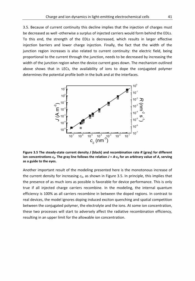
Charge and ion dynamics in light‐emitting electrochemical cells 41
3.5. Because of current continuity this decline implies that the injection of charges must
be decreased as well ‐otherwise a surplus of injected carriers would form behind the EDLs.
To this end, the strength of the EDLs is decreased, which results in larger effective
injection barriers and lower charge injection. Finally, the fact that the width of the
junction region increases is also related to current continuity: the electric field, being
proportional to the current through the junction, needs to be decreased by increasing the
width of the junction region when the device current goes down. The mechanism outlined
above shows that in LECs, the availability of ions to dope the conjugated polymer
determines the potential profile both in the bulk and at the interfaces.
Figure 3.5 The steady‐state current density J (black) and recombination rate R (gray) for different ion concentrations c0. The gray line follows the relation J = A∙c0 for an arbitrary value of A, serving as a guide to the eyes.
Another important result of the modeling presented here is the monotonous increase of
the current density for increasing c0, as shown in Figure 3.5. In principle, this implies that
the presence of as much ions as possible is favorable for device performance. This is only
true if all injected charge carriers recombine. In the modeling, the internal quantum
efficiency is 100% as all carriers recombine in between the doped regions. In contrast to
real devices, the model ignores doping induced exciton quenching and spatial competition
between the conjugated polymer, the electrolyte and the ions. At some ion concentration,
these two processes will start to adversely affect the radiative recombination efficiency,
resulting in an upper limit for the allowable ion concentration.
10-7 10-6 10-5 10-4 10-3 10-2 10-1
10-5
10-4
10-3
10-2
10-1
100
101
J (A
m-2)
c0 (nm-3)
R (nm
-2 s-1)
10-7
10-6
10-5
10-4
10-3
10-2
10-1
100

42 Chapter 3 | Salt concentration effects
Figure 3.6 Current transients of planar Au/SY‐PPV:PEO:KCF3SO3/Au LECs with an interelectrode
gap of 90 µm during operation at Vbias = 8 V. Two different SY‐PPV:PEO:KCF3SO3 weight ratios were used: (a) 1:1.35:0.25 – ion‐rich and (b) 1:1.35:0.06 – ion‐poor. The modeled current transients are from LECs with an initial homogeneous ion concentration (c0) as specified in the figures. [I0, t0] in (a) is [5 µA, 150 s] for the experiment and [1.8 A m‐2, 54 s] for the model and in (b) [5 nA, 1200 s] for the experiment and [0.15 mA m‐2, 300 s] for the model.
In order to further determine the similarity between model and experiment, the
measured and modeled current transients are presented in Figure 3.6. Characteristic
features in both the high‐ and low‐ion density curves can be decomposed in an ionic and
electronic contribution. Since the contacts are initially non‐injecting, the current density at
t = 0 can be attributed to the redistributing ions in the active layer. Thereafter, this
contribution continuously declines due to ion pile‐up at the electrodes and a decrease of
the bulk field because of the resulting EDL formation. When EDLs are being formed,
injection of electrons and holes is enhanced, resulting in an increasing electronic current.
This rise is observed in all four current transients and the resulting maximum in current is
marked by the arrows in Figure 3.6. Following this rise, a second decrease of the current
density, now related to a decrease of the electronic current, is observed. After the onset
of current injection from the contacts, a large fraction of the electronic current is
‘consumed’ for doping the device, i.e. used to compensate space charges resulting from
the further separation of anions and cations. When this doping process is completed, the
electronic current decreases. At steady‐state, anions and cations have been fully
separated into p‐ and n‐type doped regions, separated by a relatively sharp potential drop
in the junction region; see Figure 3.1, Figure 3.3, and Figure 3.6. In the modeled LECs, the
steady‐state current consists of an electronic contribution only; the ionic current has
vanished due to the ion‐blocking electrodes and the absence of generation and
recombination of ions. In principle the same holds for the real LECs, although a minor ionic
contribution from regions outside the inter‐electrode gap, having a longer settling time
due to the larger distances involved, cannot be excluded.
(a) (b)Ion rich Ion poor
0.0 0.5 1.0
0.0
0.5
1.0
I / I 0
t / t0
model: c0 = 1.5x10⁻⁶ nm-3
experiment: c0 = 7.4x10⁻² nm-3
0.0 0.5 1.00.0
0.5
1.0
experiment:
c0 = 3.1x10⁻¹ nm-3
model: c0 = 1.5x10⁻³ nm-3
I / I 0
t / t0

Charge and ion dynamics in light‐emitting electrochemical cells 43
One of the major setbacks of LECs is the relatively long response time. The present
experimental results, as well as those by Fang et al.,12 show that a decrease of c0 leads to
an increase of the response time in LECs. The same is observed in modeled LECs (Figure
3.6) in which the ion concentration becomes so low that the formation of EDLs is affected
and delayed. This is observed at the cathode in Figure 3.3d. However, current transients
accompanying the simulations presented in Figure 3.4 reveal that when EDL formation is
not hindered, the response time is independent of c0; see also Figure 3.7. This difference
between model and experiment suggests that processes omitted in the model cause the
longer response time of low ion concentration LECs. In the model, the redistribution of
ions is limited by the cations (anions) being transported from the p‐type (n‐type) doped
region to the n‐type (p‐type) doped region. The latter is only controlled by the (field
driven) drift current, and should therefore be independent of concentration, unless e.g.
side reactions hinder the movement of ions. Alternatively, it is conceivable that the ionic
mobility is concentration dependent. In either case, these results indicate that the use of a
high ion density decreases the turn‐on time.
Figure 3.7 Current transients of modeled LECs (c.f. Figure 3.4) for different values of the initial ion concentration c0.
So far, no comments have been made regarding the discrepancy between the ion
concentration used in the model and the nominal salt concentration in the active layer
during experiments. In the transient modeling presented in Figure 3.3c,d and Figure
3.6a,b, the initial ion concentrations were chosen to be 1.5∙10‐3 and 1.5∙10‐6 nm‐3 for the
high‐ and low‐ion density device, respectively. The nominal salt concentrations in the
experiments were 3.0∙10‐1 and 0.7∙10‐1 nm‐3, respectively. The latter concentration
difference of a factor of 4 resulted in a decrease of the steady‐state current by a factor 103: 1.5 µA for the ion‐rich device and 0.4 nA for the ion‐poor device. As shown in Figure
10-2 10-1 100 101 10210-4
10-3
10-2
10-1
100
101
102
103
10-5
2x10⁻⁶
10-6
10-3
10-4
Cur
rent
den
sity
(A
m-2)
Time (s)
c0 (nm-3)
10-1
10-2

44 Chapter 3 | Salt concentration effects
3.5, changing the initial ion concentration by a factor 103 in the model leads to a change in
the calculated current density by the same factor 103. Additionally, the only way to
achieve qualitatively similar current transients and potential profiles in the model and the
experiment is by using three orders of magnitude difference between high and low ion
concentrations in the model. These results imply that the effective initial mobile ion
density in a real LEC is a highly nonlinear function of the salt concentration. We speculate
that this behavior is related to the effective loss of ions in side‐reactions19, 21 and/or to the
existence of immobile ions locked up in crystalline PEO phases.22‐23
3.4 ConclusionsBy combination of experiments and numerical modeling insight is gained regarding the
function of ions in planar light‐emitting electrochemical cells. An increase of the initial ion
concentration results in an increased steady‐state current density and recombination rate
in the LEC due to the enhanced conductivity of the active layer by electrochemical doping.
Concomitant, injection is enhanced and the recombination zone is narrowed. Hence, from
a device modeling point of view, optimal performance in terms of light output at given
bias requires the use of an as high as possible ion concentration. In real devices adverse
effects like doping‐induced exciton quenching, side‐reactions and a finite solubility may
put an upper limit to the optimal ion concentration.

Charge and ion dynamics in light‐emitting electrochemical cells 45
References
[1] Q. B. Pei, G. Yu, C. Zhang, Y. Yang, A. J. Heeger, Science 269 (1995) 1086.
[2] J. M. Leger, Adv. Mater. 20 (2008) 837.
[3] L. Hu, G. Xu, Chem. Soc. Rev. 39 (2010) 3275.
[4] H. Shimotani, G. Diguet, Y. Iwasa, Appl. Phys. Lett. 86 (2005) 022104.
[5] Q. J. Sun, Y. F. Li, Q. B. Pei, J. Disp. Technol. 3 (2007) 211.
[6] O. Inganas, Chem. Soc. Rev. 39 (2010) 2633.
[7] L. He, L. A. Duan, J. A. Qiao, G. F. Dong, L. D. Wang, Y. Qiu, Chem. Mater. 22 (2010) 3535.
[8] C. Y. Lin, A. Garcia, P. Zalar, J. Z. Brzezinski, T. Q. Nguyen, J. Phys. Chem. C 114 (2010) 15786.
[9] Z. Chen, X. D. Dang, A. Gutacker, A. Garcia, H. P. Li, Y. H. Xu, L. Ying, T. Q. Nguyen, G. C. Bazan, J. Am.
Chem. Soc. 132 (2010) 12160.
[10] G. Latini, G. Winroth, S. Brovelli, S. O. McDonnell, H. L. Anderson, J. M. Mativetsky, P. Samori, F.
Cacialli, J. Appl. Phys. 107 (2010) 124509.
[11] R. Marcilla, D. Mecerreyes, G. Winroth, S. Brovelli, M. D. R. Yebra, F. Cacialli, Appl. Phys. Lett. 96
(2010).
[12] J. F. Fang, Y. L. Yang, L. Edman, Appl. Phys. Lett. 93 (2008) 063503.
[13] A. Sandstrom, P. Matyba, L. Edman, Appl. Phys. Lett. 96 (2010) 053303.
[14] Y. Shao, G. C. Bazan, A. J. Heeger, Adv. Mater. 20 (2008) 1191.
[15] J. F. Fang, P. Matyba, L. Edman, Adv. Funct. Mater. 19 (2009) 2671.
[16] S. Tang, L. Edman, J. Phys. Chem. Lett. 1 (2010) 2727.
[17] S. van Reenen, P. Matyba, A. Dzwilewski, R. A. J. Janssen, A. Edman, M. Kemerink, Adv. Funct. Mater.
21 (2011) 1795.
[18] N. D. Robinson, J. F. Fang, P. Matyba, L. Edman, Phys. Rev. B 78 (2008) 245202.
[19] J. Fang, P. Matyba, N. D. Robinson, L. Edman, J. Am. Chem. Soc. 130 (2008) 4562.
[20] D. M. de Leeuw, M. M. J. Simenon, A. R. Brown, R. E. F. Einerhand, Synth. Met. 87 (1997) 53.
[21] T. Wagberg, P. R. Hania, N. D. Robinson, J. H. Shin, P. Matyba, L. Edman, Adv. Mater. 20 (2008) 1744.
[22] P. G. Bruce, Solid State Electrochemistry. Cambridge University Press: 1995.
[23] M. Marzantowicz, J. R. Dygas, F. Krok, A. Tomaszewska, G. Z. Zukowska, Z. Florjanczyk, E. Zygadlo‐
Monikowska, Electrochim. Acta 55 (2010) 5446.

46 Chapter 3 | Salt concentration effects

*Part of the work presented in this chapter has been published: S. van Reenen, R. A. J. Janssen, M. Kemerink, Org. Electron. 12 (2011) 1746.
Chapter4 Dopingdynamicsinlight‐
emittingelectrochemicalcells
A major drawback of light‐emitting electrochemical cells (LECs) is the long time scale
associated with switching, during which ions redistribute in the active layer. We present a
numerical modeling study that gives fundamental insight in the dynamics during turn‐on.
The characteristic response of planar LECs to an applied bias is electrochemical doping of
the active layer by doping fronts moving across the active layer. Formation and motion of
such doping fronts are shown to be intimately related to both the electronic and ionic
mobility and therefore provide useful information regarding these two quantities in LECs.
In particular, it is shown that the switch‐on time in LECs is directly related to the time an
ion needs to cross approximately half the device, enabling the extraction of the ion
mobility from the switch‐on time.

48 Chapter 4 | Doping dynamics in light‐emitting electrochemical cells
4.1 IntroductionIn the previous chapters mainly quasi steady‐state operation in LECs was considered. Here
the transient operation of LECs is studied. In wide‐gap planar LECs, the transient operation
can be visualized by monitoring the PL of the active layer under UV illumination (see
Figure 3.1);1 in the presence of doping, PL is quenched in the active layer.2 Particularly
interesting is the way in which this doping occurs. Starting from the electrodes, doped
regions expand towards each other. During this expansion, doping fronts are visible as
sharp transitions between the undoped region and the n‐ and p‐type doped regions.
These fronts have been observed to accelerate. Figure 4.1a (symbols) shows a typical
measurement3 of the front position versus time.
Figure 4.1 (a) Front position during switch‐on in an LEC as obtained experimentally (symbols)3, analytically (gray line)4 and by numerical modeling (black line). The model curve follows from modeling of a planar LEC with a doping dependent µp/n according to Eq. (4.1) for µ0 = 5∙10
‐11 m2 V‐1
s‐1, µ1 = 5∙10‐8 m2 V‐1 s‐1, f0 = 0.13 and W = 0.015. (b) The electron/hole mobility as a function of the
doping fraction. The symbols were experimentally determined by Shimotani et al.5 in regioregular P3HT (here the mobility values are divided by 10
2) and the black line follows from Eq. (4.1) for µ0 = 5∙10‐11 m2 V‐1 s‐1, µ1 = 5∙10
‐9 m2 V‐1 s‐1, f0 = 0.3 and W = 0.04.
Several experimental studies6‐8 have been performed on these fronts as well as analytical4,
9 and numerical modeling.10 Robinson and co‐workers developed an analytical model that
predicts the position of the doping fronts and the resultant switch‐on time. They assumed
that both the potential over the shrinking undoped region and the conductivity through
this region remain equal. The first assumption is however not necessarily true in LECs.
Measurements of the electrostatic potential in the previous chapter (Figure 3.3a) show
that the potential does not strongly evolve during doping front progression.11 Results
presented in this chapter furthermore confirm these findings.
Here we demonstrate by numerical modeling12 that a doping dependent mobility5 is
required to generate the accelerating doping fronts observed experimentally (Figure 4.1b,
symbols). In addition the ion mobility with respect to the electron/hole mobility is critical
for front formation as well as for other transient properties like the formation of electric
Robinson
0.0 0.2 0.4 0.6 0.8 1.0
0.0
0.2
0.4
0.6
0.8
1.0
Nor
mal
ized
fron
t po
sitio
n
Normalized time
Ref 3
Model
0.01 0.1 110-11
10-10
10-9
10-8
10-7
f0
1
p/n (
m2 V
-1 s
-1)
Doping fraction
Ref 5
model
0
W
(a) (b)

Charge and ion dynamics in light‐emitting electrochemical cells 49
double layers (EDLs)13 and a light‐emitting p‐i‐n junction. For formation of accelerating
doping fronts, the ion mobility needs to be approximately equal to the electron/hole
mobility in the undoped polymer. In simulations that obey these criteria, the doping front
propagation shows an excellent agreement with experimentally observed doping fronts as
shown in Figure 4.1a (black solid line).3 As opposed to the t2 dependency of the front
position obtained by Robinson et al.4 (Figure 4.1a, gray solid line) our model shows a less
strong time dependence of the front position. Next to this fundamental understanding of
the formation of doping fronts, also the transient behavior and the switch‐on time in LECs
are rationalized by means of numerical modeling. The simulations indicate that the switch‐
on time is mostly related to the time an ion needs to cross approximately half the device.
4.2 MaterialandmethodsComputational details: The 1‐dimensional model described in detail in Appendix A was
used in which an active layer with a length of 2 µm was divided in discrete, equidistant
grid points.11‐12 Devices with a bandgap Eg = 2 eV were simulated during operation at a
bias voltage Vbias = 5 V. Simulations were run for devices with an initial homogeneous ion
concentration c0 = 1∙10‐1 nm‐3. No binding energy was assumed between anions and
cations. The electrodes were ionically‐blocking and electrons and holes were injected from
the contacts according to a dedicated injection model that gives rise to field dependent
injection.12 The injection model (modified Boltzmann) is described in detail in Appendix A
and has the advantage that injection is not affected by grid‐point spacing. The hole and
electron injection barriers were set at 0.5 and 1.5 eV respectively to simulate an
asymmetric device. Such an asymmetry is realistic for actual planar LECs, in which both the
anode and the cathode are made from a single material, e.g. Au. In addition, we set the
relative dielectric constant ε = 3 and the temperature T = 300 K.
To implement a doping density dependency of the electron/hole mobility (µp/n) the
following expression was used:
/
/ , / ,/ , . (4.1)
Here f is the doping fraction which is equal to the carrier density divided by the density of
states (= 0.3 nm‐3). Note that here the carrier density is assumed to represent the doping
density. This approximation of the doping fraction is justified by the observation that the
net ion density always equals the net electronic charge density in the doped regions.
Regarding the other parameters, µp/n,1 is the mobility at maximal doping (f = 1), µp/n,0 is the
mobility in the absence of doping (f = 0), and f0 and W are two parameters that set the
transition from µ0 and µ1: f0 determines at which doping fraction the mobility increases
and W determines the range of doping fractions over which this increase occurs. Figure

50 Chapter 4 | Doping dynamics in light‐emitting electrochemical cells
4.1b (line) shows a typical plot of the doping dependent mobility that follows from Eq.
(4.1) for f0 = 0.3, W = 0.04, µ0 = 5∙10‐11
m2 V‐1 s‐1 and µ1 = 5∙10
‐9 m2 V‐1 s‐1. The anion and
cation mobilities were chosen to be equal to each other and doping independent. Ion
mobilities ranged from 5∙10‐12 to 5∙10‐9 m2 V‐1 s‐1.
Since our interest is the transient behavior of LECs, simulations started with the
application of a bias voltage on a homogeneous device and were continued until steady‐
state was reached. At t = 0 the electron and hole density equals zero and the anion and
cation density equals c0. It was checked that the inter‐electrode gap and meshing did not
affect the outcome of the simulations in any non‐trivial manner.
4.3 ResultsanddiscussionMultiple simulations were performed to analyze the effect of the electronic and ionic
mobilities on the transient behavior in LECs and specifically on the formation of doping
fronts. The time‐evolution of the electron and hole density profiles that follow from these
simulations are shown in Figure 4.2. The absence (Figure 4.2a‐d) and presence (Figure
4.2e‐f) of a doping dependent mobility was studied as well as the effect of the ion
mobility. The doping dependent mobility that is shown in Figure 4.1b (model) was used in
these simulations. It will be shown below that the qualitative behavior in these
simulations only depends on the relative values of the mobilities of the electronic and
ionic species.
Starting from t = 0, the processes in these devices are similar: anions and cations move
towards the anode and cathode respectively forming EDLs (see supplemental Figure 4.9 in
paragraph 4.5). When the resultant potential drop at the interfaces has become similar in
size to the injection barriers, charge carriers start being injected. During EDL formation,
the anion and cation concentrations in the bulk remain equal to maintain charge
neutrality. Only at the electrodes this neutrality is broken because of depletion of one
type of ion and accumulation of the other. During the subsequent injection of either
electrons or holes, a third type of charge carrier comes into play. To maintain charge
neutrality in the bulk, the anion and cation densities start to differ. At this stage, where
injection of carriers is initiated, differences in the transient processes arise when ion or
carrier mobilities are altered.
When interpreting the results shown in Figure 4.2, the discussion focuses on two
characteristics: (1) the collision of the p‐type and n‐type doped regions and (2) the
saturation of doping at each grid‐point after the doping front has passed. Here, doping is
saturated when a doping fraction of approximately 0.2‐0.3 is reached, i.e. at a charge
density of 2‐3∙10‐1∙0.3 nm‐3 in Figure 4.2. Note that in experiments, strong PL quenching is

Charge and ion dynamics in light‐emitting electrochemical cells 51
observed when the doping density reaches a threshold level; PL quenching is not
necessarily linear with doping fraction.1
Figure 4.2 Transient carrier concentration profiles in LECs for (a)‐(d) a constant µp/n equal to 5∙10‐11
m2 V‐1 s‐1 and (e)‐(h) a doping dependent µp/n (see Figure 4.1b, model). Holes (open circles) are injected from the left and electrons (closed circles) from the right. The corresponding values of µion are shown at the top of each panel expressed in m2 V‐1 s‐1. The movement in time is expressed by the color change of the graphs from light gray to black. The final black curves are not the steady‐state distributions but represent the moment the fronts meet.
As a first example, we show in Figure 4.2b, the time evolution of the doping of the active
layer assuming a doping‐independent mobility of µion = µp/n = 5∙10‐11 m2 V‐1 s‐1. No sharp
transitions are observed from doped to undoped regions: the doped regions already
connect to each other while the doping density in roughly half the cell is far from
saturated. However, in case of a doping dependent mobility µp/n (Figure 4.2f), the
transition between the doped and undoped regions is sharper; the increased mobility of
electrons and holes injected behind the front results in a faster saturation of doping
compared to the progression of the doped region through the intrinsic region. The
enhanced mobility behind the front also ensures a sufficient supply of carriers towards the
fronts to prevent a decrease of the doping rate at the front. In contrast to the situation for
a doping‐independent mobility (Figure 4.2b), the time needed to completely dope the
10-5
10-3
10-1
10-5
10-3
10-1
µion = 5·10-12
5·10-11
10-5
10-3
10-1
5·10-10
0 500 1000 1500 200010-5
10-3
10-1
5·10-9
10-5
10-3
10-1
10-5
10-3
10-1
10-5
10-3
10-1
0 500 1000 1500 200010-5
10-3
10-1
5·10-12
5·10-11
5·10-10
5·10-9
Position (nm)
Charge den
sity (x0.3 nm
‐3)
(a)
(b)
(c)
(d)
(e)
(f)
(g)
(h)
Constant µp/n Doping dependent µp/n

52 Chapter 4 | Doping dynamics in light‐emitting electrochemical cells
active layer in Figure 4.2f is limited by the front progression and not by the process of
saturating the doping behind the fronts.
When the ion mobility is decreased by a factor 10 (µion = 5∙10‐12 m2 V‐1 s‐1, Figure 4.2a and
e) both doping regions come into contact even before doping has saturated at any
position in the cell. No sharp transitions are observed from doped to undoped regions.
These observations are the result of the relative immobility of the ions compared to the
electrons and holes, which mainly hampers the actual doping of the active layer. Since
µp/n,0 > µion progression of the electronic charges through the device is fast relative to the
actual doping at any fixed position in the device. Consequently there is a small doping
density difference between the front and the doped regions just behind it, which results in
only a minor carrier mobility enhancement behind the front. Therefore, the carriers
behind the front are not propelled towards the front as was observed in Figure 4.2f. For
that reason, the two doping fronts have already moved across the active layer while the
doping process is far from finished. After the doped regions have met, doping saturates
more or less evenly throughout the LEC. This result indicates that if µion < µp/n,0
homogeneous doping of the active layer is found rather than doping by doping fronts.
On the other hand, when the ion mobility is increased by a factor 10 (µion = 5∙10‐10 m2 V‐1 s‐
1, Figure 4.2c and g), sharp doping fronts are formed for both a density dependent and a
density independent µp/n. The origin of the formation of these sharp fronts is however
different as compared to the fronts formed in Figure 4.2f. In case a constant µp/n is chosen
(Figure 4.2c) anions and cations always move faster than the injected carriers. As a result,
the available anions and cations are able to electrostatically compensate the injected
carriers relatively fast. As shown in the previous chapter in Figure 3.3d,12 in the absence of
injected carriers, because of e.g. relatively poor carrier injection, the ions tend to screen
the bulk from the electric field. Here this tendency is observed during doping of the active
layer: the electric field Ei in the intrinsic region, that drives the doping front, is reduced by
ion screening (see e.g. the slope of the potential at x = 1000 nm for the light gray graphs in
supplemental Figure 4.7c at the last paragraph of this chapter). Accordingly the carriers at
the fronts are slowed down, while newly injected carriers in the already doped regions are
accelerated because of a locally enhanced field. (see the slope of the potential at x = 300
for the dark gray graphs in supplemental Figure 4.7c). This combination results in a sharp
doping front. For a doping dependent mobility (Figure 4.2g), the same behavior of the ions
is observed; ions accumulate at the front to screen the intrinsic region from the applied
field. In addition, in this case the doping‐enhanced mobility of injected carriers is larger
than the ion mobility. Hence, these carriers can more easily approach the carriers at the
front, which further sharpens the doping front in Figure 4.2g as compared to Figure 4.2c.
(see supplemental Figure 4.8 for an evaluation of the sharpness of the n‐type doping front
during propagation).

Charge and ion dynamics in light‐emitting electrochemical cells 53
In case the ion mobility is increased even more, i.e. 5∙10‐9 m2 V‐1 s‐1, the effects of a
reduction of Ei become more pronounced, as shown by relatively large doping density
close to the electrodes in Figure 4.2d and h. Furthermore, the strong depletion of ions
from the intrinsic region becomes a limiting factor. The regions close to the electrodes
absorb most of the ions and hence they are not directly available for electrochemical
doping. Consequently, the doping fronts slow down as no more ions are available in the
intrinsic region. After that, ions from the already doped regions are transported
backwards to the front to complete the doping. (the ion density profiles are shown in
supplemental Figure 4.9). This backward ion transport is driven by the inward movement
of electrons and holes.
It is important to point out that the steady‐state carrier distributions and potential profiles
are the same for each ion mobility as the ion mobility only affects the transient
characteristics in LECs, not the steady‐state characteristics.12 The graphs in Figure 4.2 are
plotted until the p‐i‐n junction has formed, hence the black curves do not represent
complete equilibrium.
The positions of the sharp doping fronts observed in Figure 4.2 are plotted vs. time in
Figure 4.3a. For each doping profile in Figure 4.2 the position at which the doping density
equaled a constant, arbitrarily chosen value of 3∙10‐3 nm‐3 was taken to produce Figure
4.3a. A different choice of this value hardly affects the doping front propagation profiles in
Figure 4.3a, because the shape of the doping density profile is more or less constant
during doping front propagation (see e.g. Figure 4.2g). The observed acceleration
(superlinear behavior in Figure 4.3a,c) or deceleration (sublinear behavior) of the sharp
doping fronts can be related to the origins of sharp front formation as discussed above. A
reduction of the electric field and/or ion density in the intrinsic region was found to
underlay the fronts observed in panels c, d, g, and h of Figure 4.2. Both these effects
directly lead to a deceleration of the doping front. Consequently, newly injected carriers
have time enough to dope the region behind the front and thus maintain a constant
doping density from the electrodes towards the fronts, which is perceived as a sharp
doping front. In case sharp doping fronts are formed because the mobility of newly
injected carriers is enhanced (Figure 4.2f), the doping front velocity is observed to slightly
increase with time because of the large supply of injected carriers. These effects or
combinations of these effects can be observed in the front position vs. time plots in Figure
4.3a. Consider the front position vs. time graphs for a doping‐dependent mobility (circles).
For µion = 5∙10‐9 m2 V‐1 s‐1 (light gray circles) the front speed declines because of a reduction
of both Ei and ion density in the intrinsic region. For µion = 5∙10‐10 m2 V‐1 s‐1 (dark gray
circles) the front speed is constant, being the sum of opposite effects: a reduction of Ei
and an enhancement of µp/n in the doped regions. For µion = µp/n,0 = 5∙10‐11 m2 V‐1 s‐1 (black
circles), the front speed increases, because µp/n is enhanced. The latter, an increasing front

54 Chapter 4 | Doping dynamics in light‐emitting electrochemical cells
speed, is in agreement with published experimental data, see Figure 4.1a.4 In case µp/n is
doping‐independent (squares), the front speed mainly declines because of the reduction
of Ei and ion density in the intrinsic regions.
Figure 4.3 Calculated doping front position vs. time plots in LECs for different carrier mobility functions. The p‐ and n‐type doping fronts are denoted by the open and closed circles respectively. (a) The doping front propagation for different values of µion as indicated in the legend in m2 V‐1 s‐1. The circles and squares correspond to a density dependent and independent µp/n respectively. (b) Different doping dependent mobility functions for which µ0 = 5∙10
‐11 m2 V‐1 s‐1, µ1 = 5∙10‐9 m2 V‐1 s‐1, W = 0.04/0.03/0.02/0.015 and f0 = 0.3/0.22/0.14/0.10. For the modeled experimental curve W = 0.015, f0 = 0.13 and µ1 = 5∙10
‐8 m2 V‐1 s‐1 were taken. (c) The doping front propagation for the different doping dependent mobility functions shown in (b). (d) Schematic of the ion mobility criteria with respect to the doping dependent electron and hole mobility (gray line) that result in the formation of accelerating doping fronts in LECs during switch‐on.
To study the effect of a sharper mobility increase as a function of doping, simulations were
performed in which parameters W and f0 in Equation (4.1) were decreased. The mobility
curves are shown in Figure 4.3b. Simulations of the front propagation were performed for
all these curves while µion = 5∙10‐11 m2 V‐1 s‐1. The results are shown in Figure 4.3c. If the
mobility increase becomes sharper with respect to an increased doping density, the time
needed for both fronts to meet each other clearly decreases. Furthermore, also a larger
acceleration of the fronts is observed. These observations are related to the enhanced
carrier mobility at progressively lower doping levels: the higher carrier mobility behind the
0 1 2 3 4 50
500
1000
1500
2000
Fro
nt p
ositi
on (
nm)
Time (ms)
W=0.04 W=0.03 W=0.02 W=0.015 Modeled exp.
curve
0 1 2 3 4 5 60
500
1000
1500
2000
5·10-9
5·10-10
5·10-11
5·10-9
5·10-10Fro
nt p
osi
tion
(nm
)
Time (ms)0.01 0.1 1
10-11
10-10
10-9
10-8
10-7
p/n (
m2 V
-1 s
-1)
Doping fraction
W=0.04 W=0.03 W=0.02 W=0.015 modeled exp. curve exp. curve
0.0 0.2 0.4 0.6 0.8 1.0
10-2
10-1
100
101
102
ion
/
p/n,
0
Doping fraction
No doping fronts
Accelerating doping fronts
Decelerating doping fronts
p/n
(a) (b)
(c) (d)
Constant µp/n
Doping dependent µp/n

Charge and ion dynamics in light‐emitting electrochemical cells 55
front results in an increased supply of carriers for doping at the fronts, enabling the front
to move faster through the active layer. Also a simulation was performed with a doping
dependency of the mobility that mimics the experimental mobility curve in Figure 4.1b
(see ‘modeled exp. Curve’ in Figure 4.3b). The resultant front position vs. time curve is
shown in Figure 4.3c. This result was normalized and plotted in Figure 4.1a to enable
comparison with the experiment.4 A striking similarity is observed, constituting the validity
of the model. Furthermore, it shows that the chosen mobility dependency seems
qualitatively correct in describing front propagation in LECs. Furthermore, it was checked
by additional simulations that the results do not qualitatively depend on the ion
concentration or the device length. Quantitatively, an increase of c0 results in faster
movement of the fronts through the device. This effect originates from the availability of
more ions to dope the organic semiconductor, thereby increasing the rate of doping
behind the fronts. The consequently increased doping density results in an increased
supply rate of carriers towards the fronts that effectively increases the doping front
propagation.
The phase diagram shown in Figure 4.3d summarizes the results shown in Figure 4.2 and
Figure 4.3a‐c. In the diagram the doping dependent µp/n is shown relative to µp/n,0.
Dependent on the ratio between µion and µp/n,0, three regions can be identified: (1) for µion
<< µp/n,0 no doping fronts are formed; (2) for µion ≈ µp/n,0 accelerating doping fronts are
formed; and (3) for µion >> µp/n,0 decelerating doping fronts are formed. For a constant µp/n
the central region disappears so either no or decelerating doping fronts are formed. As
already mentioned, experiments on planar LECs have indicated the formation of doping
fronts during turn‐on that accelerate when closing in on each other.3 Combination of
these experimental results with our numerical modeling strongly indicates that µp/n
depends similarly on doping and that µion is of the same order as µp/n,0.
From the simulations presented in Figure 4.2e‐h current vs. time plots were made to study
the transient behavior in LECs with a doping dependent mobility for varying ion mobility. A
typical plot is shown in Figure 4.4. The ionic and electronic contributions to the current are
plotted separately as well to make the total current transient more comprehensive. At t =
0, the current is completely carried by the ions. These ions first form the EDLs at the
electrodes, resulting in injection of holes (marked with arrow 1 in Figure 4.4) and electrons
(arrow 2). Electron injection is delayed compared to hole injection because of the larger
injection barrier that needs to be overcome by formation of a larger EDL. This injection
results in an increased electronic current. Following this injection, the active layer is
doped, during which the ionic current is observed to slowly decrease and the electronic
current to increase. The initiation of recombination (diamond symbols in Figure 4.4)
indicates that the doping fronts have met (arrow 3). After this, both recombination and
the electronic current increase.14 This indicates the further doping of the active layer until

56 Chapter 4 | Doping dynamics in light‐emitting electrochemical cells
at some time the current as well as the recombination suddenly drop (arrow 4). This is
related to a change in the electric field distribution after which the externally applied
electric field becomes concentrated in the recombination region rather than being
distributed over the entire active layer: The p‐i‐n junction has formed. Hence, meeting of
the doping front does not coincide with but precedes the formation of a p‐i‐n junction.
The appearance of a sharp potential drop in the p‐i‐n junction arises from the anions and
cations being completely removed from the junction region.12 These ions have been used
to maximize doping in the surrounding regions. Because of the relatively small density of
carriers in the recombination region, the conductivity is relatively low compared to the
doped regions. Therefore, in order to fulfill current conservation, a larger field is required
in the junction region rather than the doped regions.
Figure 4.4 Calculated J, t and R, t characteristics in an LEC for µion = 5∙10‐11 m2 V‐1 s‐1 (c.f. Figure 4.2f)
and a doping dependent µp/n (c.f. Figure 4.1b). The square, circle, triangle and diamond graphs represent the total current density Jtotal, the ion current density Jion, the electron and hole current density Jp/n and the recombination rate R respectively. 1, 2, 3, and 4 refer to initiation of hole injection, initiation of electron injection, front meeting and formation of a light‐emitting p‐i‐n junction respectively.
The time between the application of a bias and the injection of holes, the injection of
electrons, the doping front meeting and the p‐i‐n junction formation is plotted in Figure
4.5 as a function of µion relative to µp/n,0. The results in Figure 4.5a and b correspond,
respectively, to simulations with a constant and doping dependent µp/n. The time is
normalized by the time an ion needs to travel across the device in the presence of an
(average) field equal to (Vbias – Eg)/L. A horizontal line in these graphs indicates that the
time needed for the corresponding process depends linearly on µion and bias. Accordingly,
the graphs show that the time needed for the initiation of electron and hole injection
linearly depends on µion. This can also be easily deduced from the fact that injection of
carriers is directly related to the formation of EDLs, which results from a reorganization of
the ion density across the device. The meeting of the doping fronts that follows after
Jtotal
Jp/n
Jion
R
10-4 10-3 10-210-4
10-2
100
102
104
Cur
rent
den
sity
(A
m-2)
Time (s)
1
23
4
10-9
10-8
10-7
Re
com
bin
atio
n ra
te (
nm
-2 s
-1)

Charge and ion dynamics in light‐emitting electrochemical cells 57
injection of carriers is however not linearly related to µion. Doping of the active layer is
related to both µp/n and µion. This is unlike the conclusion drawn by Robinson et al. that
mainly ionic movement in the intrinsic region determines the time needed to dope the
active layer.4 Rather, the doping front propagation is determined on one hand by the
electron/hole transport in the doped regions and at the doping front, and on the other
hand by the ion transport in the intrinsic region. Formation of a light‐emitting p‐i‐n
junction (process 4) is observed to be linearly dependent on µion at small values of µion /
µp/n,0. Dependent on the presence or absence of a doping dependence, this linear
dependence exists in Figure 4.5a for µion / µp/n,0 < 1 and in Figure 4.5b for µion / µp/n,0 < 10.
This process is namely related to ion depletion from the recombination zone, which
causes the linear dependence in µion. This ion depletion can only occur when the transfer
of mobile anions (cations) from the n‐type (p‐type) doped region to the p‐type (n‐type)
doped region is completed. For this to complete, the largest distance ions need to travel in
a mostly symmetric device is a bit more than half the device length. A value of ti∙µion∙(V‐
Eg)∙L‐2 ~ 0.6 is found in the modeling shown in Figure 4.5 (black graphs, numbered 4). For
large µion / µp/n,0, corresponding to slow electronic carriers, the formation of a light‐
emitting p‐i‐n junction is no longer limited by ion depletion, but is limited by the meeting
of the doping fronts. In this case, the ions are already depleted from the recombination
region before the fronts have met, which is determined by the slow electronic charge
carriers.
Figure 4.5 Time scale comparison for four characteristic processes in LECs for different values of µion / µp/n,0 in case of (a) no doping dependent carrier mobility and (b) a doping dependent carrier mobility. 1, 2, 3, and 4 (c.f. Figure 4.4) refer to initiation of hole injection, initiation of electron injection, front meeting and formation of a light‐emitting p‐i‐n junction, respectively. The dashed lines highlight the transition in behavior of the time needed for junction formation (4).
The transition point (Figure 4.5a: µion / µp/n,0 ≈ 1; Figure 4.5b: µion / µp/n,0 ≈ 5‐10) at which
the switch‐on time in LECs becomes dependent on the doping front propagation is related
to the choice of the doping dependency of µp/n. In the simulations from which Figure 4.5b
is constructed, the doping fractions in case doping is nearly saturated lies in between 0.2
0.1 1 10 1000.01
0.1
1
10
t i io
n (
V-E
g)
L-2
ion
/ p/n,0
i = 1 2 3 4
(a) (b)
0.1 1 10 1000.01
0.1
1
10
i = 1 2 3 4
t i io
n (
V-E
g)
L-2
ion
/ p/n,0
Constant µp/n Doping dependent µp/n

58 Chapter 4 | Doping dynamics in light‐emitting electrochemical cells
and 0.3, which can be translated to µp/n ≈ 10∙µp/n,0 following Eq. (4.1). This effective
mobility in the doped regions determines the transition point. In case of a doping
independent µp/n, the effective mobility is equal to µp/n and the transition point is thus
expected at µion / µp/n,0 = 1. This is indeed the case in our model (see Figure 4.5a).
In the previous chapter11 results on a planar ion rich LEC were presented in which a
significant amount of time was observed between initiation of light emission (at t = 10 s),
i.e. meeting of the doping fronts, and the formation of a p‐i‐n junction (at t = 20 s).
Comparison of those results (Figure 3.1) with the modeling presented here in Figure 4.5b
indicates that µion / µp/n,0 < 10, as the 10 s time difference proves that p‐i‐n junction
formation was not limited by doping front propagation. Therefore, the switch‐on time of
this LEC can be used to estimate the ion mobility, as 0.6
must hold. For L = 100 µm and Vbias = 8 V and Eg ≈ 2 eV, the ion mobility is then estimated
to be 5∙10‐11 m2 V‐1 s‐1 at a temperature of 323 K. The conclusion that µion / µp/n,0 < 10 is
also consistent with the discussion of Figure 4.3b since in these devices accelerating
doping fronts are typically observed. More particularly, from the parameter window for
accelerating doping fronts it can, with some caution, be estimated that the electronic
charge carrier mobility in PPV‐based LECs is also of the order of 5∙10‐11 m2 V‐1 s‐1, which is
surprisingly close to typical values for pure PPV derivatives.15‐16 A further comparison can
be done between the experimental results on the planar ion rich LEC in the previous
chapter and the simulation results shown in Figure 4.2f, Figure 4.4 and supplemental
Figure 4.7f. First of all the potential profile evolution is similar: The potential distribution
(see supplemental Figure 4.7f) hardly changes during doping front propagation. Also the
current response to an applied bias voltage (see Figure 4.4) is the same in both
experiment and model. These results further prove that the experiment is adequately
modeled.
One deviating experiment in literature is reported in which the doping fronts were found
to have a constant speed.17 Gao et al. did measurements on such an LEC, which has an
inter‐electrode distance of 2 mm and is biased at 200 V. Our modeling shows that in case a
constant front speed is encountered, µion must be large relative to µp/n,0 (see Figure 4.2g
and Figure 4.3a). Inspection of Figure 4.5b furthermore shows that the doping process in
such an LEC is not limited by the ion redistribution, but by the electronic carrier mobility.
A side‐note on the mobility discussion above is that rather than a single, constant ion
mobility, a range of ion mobilities is expected in such LECs, which further may differ for
anions and cations. The determined ion mobility therefore applies to the most mobile
fraction of ions. This hypothesis is in agreement with the finding in Ref. 11 that the actual
amount of mobile ions is far less than the amount of ions put into the active layer.

Charge and ion dynamics in light‐emitting electrochemical cells 59
4.4 ConclusionsNumerical modeling has shown that the time needed for LECs to electrochemically dope
the active layer and switch‐on depends on a combination of the ion mobility, the
electron/hole mobility, the applied bias voltage and the thickness of the active layer.
Regarding the doping process three regimes were identified, related to the mobilities of all
present charge carriers. If µion > µp/n, the active layer is doped by decelerating doping
fronts sweeping the active layer, whereas if µion < µp/n the active layer is doped
homogeneously across the complete device. Only in case a doping dependent µp/n is
chosen in addition to µion being approximately equal to µp/n in the undoped state (µp/n,0),
accelerating doping fronts are formed.
The switch‐on time in LECs is shown to become independent of µp/n when the ratio
between µion / µp/n becomes small enough. For a doping independent µp/n this critical ratio
is unity, whereas in case of a doping dependent µp/n, µion < ~10∙µp/n,0. Generally the latter
occurs in planar LECs where accelerating doping fronts are often observed. This enables
the extraction of the ion mobility from the switch‐on time of LECs.

60 Chapter 4 | Doping dynamics in light‐emitting electrochemical cells
4.5 Supplementalfigures
Figure 4.6 Calculated transient net charge density profiles in LECs from start to end of the doping front propagation (c.f. Figure 4.2). Simulations were done with a doping dependent µp/n. The corresponding values of µion are shown at the top of each graph expressed in m
2 V‐1 s‐1. The movement in time is expressed by the color change of the graphs from light gray to black. The arrows indicate a surplus of electronic carriers (1) and ionic carriers (2).
0 500 1000 1500 2000-6
-4
-2
0
2
4
6
0 500 1000 1500 2000-10
-8
-6
-4
-2
0
2
4
6
8
10
0 500 1000 1500 2000-2
0
2
4
6
8
10
0 500 1000 1500 2000-20
-15
-10
-5
0
5
10
15
20
1
1
1
2
2
µion = 5·10-12 5·10-11
5·10-10 5·10-9
(a) (b)
(c) (d)
Position (nm)
Net charge den
sity (x1021m
‐3)

Charge and ion dynamics in light‐emitting electrochemical cells 61
Figure 4.7 Calculated transient potential profiles in LECs from start to end of the doping front propagation (c.f. Figure 4.2). Simulations were done with (a)‐(d) a constant µp/n and with (e)‐(h) a doping dependent µp/n. The corresponding values of µion are shown at the top of each graph expressed in m2 V‐1 s‐1. The movement in time is expressed by the color change of the graphs from light gray to black.
-5
-4
-3
-2
-1
05·10-12
-5
-4
-3
-2
-1
05·10-11
-5
-4
-3
-2
-1
0
5·10-10
0 500 1000 1500 2000-5
-4
-3
-2
-1
0
5·10-9
-5
-4
-3
-2
-1
0
-5
-4
-3
-2
-1
0
-5
-4
-3
-2
-1
0
0 500 1000 1500 2000-5
-4
-3
-2
-1
0
µion = 5·10-12
5·10-11
5·10-10
5·10-9
Position (nm)
Potential (eV)
(a)
(b)
(c)
(d)
(e)
(f)
(g)
(h)
Constant µp/n Doping dependent µp/n

62 Chapter 4 | Doping dynamics in light‐emitting electrochemical cells
Figure 4.8 Calculated sharpness of the n‐type doping front during doping front propagation (c.f. Figure 4.2). Simulations were done with (a)‐(d) a constant µp/n and with (e)‐(h) a doping dependent µp/n. The corresponding values of µion are shown at the top of each graph expressed in m2 V‐1 s‐1. The movement in time is expressed by the color change of the graphs from light gray to black. The front sharpness is calculated by differentiating the logarithm of the electron density, n, as shown in Figure 4.2 with respect to the position. Dashed lines are added to graphs (c), (d), (f)‐(h) to indicate the sharpness (magnitude) and position (where the line crosses the data) of the doping front during propagation.
0.00
0.02
0.04
0.06
0.00
0.02
0.04
0.06
0.00
0.02
0.04
0.06
1000 1200 1400 1600 1800 20000.00
0.02
0.04
0.06
1000 1200 1400 1600 1800 2000
5·10-12
5·10-11
5·10-10
5·10-9
µion = 5·10-12
5·10-11
5·10-10
5·10-9
Position (nm)
d log n/ dx(a.u.)
(a)
(b)
(c)
(d)
(e)
(f)
(g)
(h)
Constant µp/n Doping dependent µp/n

Charge and ion dynamics in light‐emitting electrochemical cells 63
Figure 4.9 Calculated transient ion density profiles in LECs during doping front propagation for a doping dependent µp/n. The corresponding values of µion are shown at the top of each graph expressed in m2V‐1s‐1. The movement in time is expressed by the color change of the graphs from light gray to black. The closed and open circles represent the anion and cation density respectively. Arrows indicate the time progression as well.
0 500 1000 1500 20000.00
0.05
0.10
0.15
0 500 1000 1500 20000.00
0.05
0.10
0.15
0 500 1000 1500 20000.00
0.05
0.10
0.15
0 500 1000 1500 20000.00
0.05
0.10
0.15
5·10-10 5·10-9
µion = 5·10-12 5·10-11(a) (b)
(c) (d)
Position (nm)
Ion den
sity (nm
‐3)

64 Chapter 4 | Doping dynamics in light‐emitting electrochemical cells
References
[1] J. Gao, J. Dane, Appl. Phys. Lett. 84 (2004) 2778.
[2] A. L. Holt, J. M. Leger, S. A. Carter, J. Chem. Phys. 123 (2005) 044704.
[3] J. H. Shin, N. D. Robinson, S. Xiao, L. Edman, Adv. Funct. Mater. 17 (2007) 1807.
[4] N. D. Robinson, J. H. Shin, M. Berggren, L. Edman, Phys. Rev. B 74 (2006) 155210.
[5] H. Shimotani, G. Diguet, Y. Iwasa, Appl. Phys. Lett. 86 (2005) 022104.
[6] J. Gao, J. Dane, J. Appl. Phys. 98 (2005) 063513.
[7] D. Hohertz, J. Gao, Adv. Mater. 20 (2008) 3298.
[8] J. F. Fang, Y. L. Yang, L. Edman, Appl. Phys. Lett. 93 (2008) 063503.
[9] N. D. Robinson, J. F. Fang, P. Matyba, L. Edman, Phys. Rev. B 78 (2008) 245202.
[10] M. Modestov, V. Bychkov, G. Brodin, D. Valiev, M. Marklund, P. Matyba, L. Edman, Phys. Rev. B 81
(2010) 081203.
[11] S. van Reenen, P. Matyba, A. Dzwilewski, R. A. J. Janssen, A. Edman, M. Kemerink, Adv. Funct. Mater.
21 (2011) 1795.
[12] S. van Reenen, P. Matyba, A. Dzwilewski, R. A. J. Janssen, L. Edman, M. Kemerink, J. Am. Chem. Soc.
132 (2010) 13776.
[13] J. C. deMello, N. Tessler, S. C. Graham, R. H. Friend, Phys. Rev. B 57 (1998) 12951.
[14] J. Gao, Y. F. Hu, J. Am. Chem. Soc. 133 (2011) 2227.
[15] E. Lebedev, T. Dittrich, V. PetrovaKoch, S. Karg, W. Brutting, Appl. Phys. Lett. 71 (1997) 2686.
[16] E. Pinotti, A. Sassella, A. Borghesi, R. Tubino, Synth. Met. 122 (2001) 169.
[17] J. Dane, C. Tracy, J. Gao, Appl. Phys. Lett. 86 (2005) 153509.

*Part of the work presented in this chapter has been published: S. van Reenen, R. A. J. Janssen, M. Kemerink, Adv. Funct. Mater. 22 (2012) 4547.
Chapter5 Dynamicprocessesinstacked
polymerLECs
The operational mechanism of polymer LECs in sandwich geometry is studied by
admittance spectroscopy and numerical modeling. Capacitance and conductance at
different frequencies and bias voltages indicate the conduction of ions, electric double
layer formation and p‐i‐n junction formation which is all in line with the electrochemical
doping model. Numerical modeling shows that impedance measurements cannot be used
to determine the actual junction width. In addition, the long settling time of polymer LECs
is shown to be due to a slow process of salt dissociation that continues after p‐i‐n junction
formation, rather than ion conduction. This implies that in order to significantly decrease
the response‐time of LECs an electrolyte/salt combination with an as low as possible ion
binding energy must be used.

66 Chapter 5 | Dynamic processes in stacked polymer LECs
5.1 IntroductionThe electrochemical doping model has been convincingly proved in the previous chapters
for planar polymer LECs in which scanning Kelvin probe microscopy could be used to
visualize the characteristic potential shape:1‐4 a p‐i‐n junction results in a high field in the
intrinsic region and low field in the doped regions. LECs that are relevant for practical use
have however a stacked structure, in which the active layer thickness is only a few
hundreds of nanometers. This thickness difference forbids the direct translation of the
electrochemical doping model from planar LECs to stacked LECs by simply reducing the
thicknesses of the different regions. For instance, the recombination zone width found in
planar LECs typically exceeds the layer thickness of stacked LECs.3
One method to study the operation mechanism in stacked LECs is impedance
spectroscopy. As this method uses a time‐dependent signal, it is possible to look
separately at fast and slow processes in LECs. This makes impedance spectroscopy
potentially an excellent technique to disentangle the various ongoing processes in
operational LECs.5‐11 However, the data generated by this technique is generally rather
complicated and difficult to interpret. The work done on impedance spectroscopy in LECs
has so far mainly focused on the junction width during operation. In polymer LECs junction
widths between 10% and 80% of the active layer have been reported.6, 9 Furthermore,
previous modeling studies to LECs were limited to steady‐state.4, 12‐16 Recently a study on
sandwich LECs was published by Munar et al. in which equivalent circuit modeling was
used to shed light on the LEC impedance spectrum.17 However, interpretation of such
modeling results is complicated by the sometimes intransparent physical meaning of the
components. In particular, (combinations of) space charge and transit time effects tend to
give rise to ‘inductive’ responses that are hard to capture in equivalent RC networks.6, 18
Here impedance spectroscopy is combined with numerical drift‐diffusion modeling of
polymer light‐emitting electrochemical cells in stacked or sandwich geometry. We
demonstrate that the observations are fully consistent with the electrochemical doping
model. Information regarding the electric double layers (EDLs), ion conduction and the
junction region is obtained. Furthermore, our results show that the width of the
recombination region cannot be simply extracted from the intermediate‐ or high‐
frequency capacitance: there is no abrupt transition from the doped regions to the
intrinsic recombination region. The doping close to the junction region is not as dense as it
is near the contacts. This can lead to a conductivity difference of a factor >10 throughout
the doped regions. Moreover, we identify the dissociation of salt molecules into anions
and cations as the slow process that is responsible for the characteristic long settling time
of LECs.

Charge and ion dynamics in light‐emitting electrochemical cells 67
5.2 MaterialandmethodsDevice preparation: For the conjugated polymer in the active layer of our sandwich LECs
either poly[2‐methoxy‐5‐(3’,7’‐dimethyloctyloxy)‐p‐phenylene vinylene] (MDMO‐PPV, Mw
> 1∙106 g mol‐1, American Dye Source) or a phenyl‐substituted poly(p‐phenylene vinylene)
copolymer (SY‐PPV, Merck, catalogue number PDY‐132), commonly termed “Super
Yellow” was used. Poly(ethylene oxide) (PEO, Mw = 5∙105 g mol‐1, Aldrich) was used as
received. The salt potassium trifluoromethanesulfonate (KCF3SO3, 98 %, Aldrich) was dried
at 473 K under vacuum before use. MDMO‐PPV (10 mg ml‐1) and SY‐PPV (5 mg ml‐1) were
dissolved in chloroform (> 99 %, anhydrous, Aldrich). PEO and KCF3SO3 were dissolved
separately (10 mg ml‐1) in cyclohexanone (> 99 %, anhydrous, Aldrich). These solutions
were mixed together in a weight ratio of PPV:PEO:KCF3SO3 = 1:1.35:0.25. These blend
solutions were thereafter stirred on a magnetic hot plate at a temperature T = 323 K for 5
h.
ITO patterned substrates were spin‐coated with the blend solution at 800 rpm for 60 s,
followed by 1000 rpm for 10 s after which they were dried on a hot plate at T = 323 K for
at least 1 h. The resulting active layer thickness was 200‐250 nm for MDMO‐PPV LECs and
100 nm for SY‐PPV LECs, as determined by profilometry. Al electrodes were deposited by
thermal evaporation under high vacuum on top of the spin‐coated films. The final device
area was 0.091 cm2. All the above procedures, except for the cleaning of the substrates,
were done in a glove box under N2 atmosphere ([O2] < 1 ppm and [H2O] < 1 ppm) or in an
integrated thermal evaporator.
Electrical characterization: A Keithley 2636a sourcemeter was used to drive the devices
and measure the current. The brightness was measured with a luminance meter (LS‐110
Konica‐Minolta). A Solartron 1260 was used to perform complex admittance
measurements on the LECs in the glove box at room temperature. After applying a bias,
cells were allowed to settle for 1 minute before the admittance spectrum was measured.
Each point (from 30 MHz to 1Hz) was measured during an integration time of 1 s. The rms‐
value of the AC voltage was 0.01 V.
Computational details: For the numerical simulations, the 1‐dimensional model was used
which is described in detail in Appendix A. An active layer of length L = 200 nm was divided
in N = 99 discrete points. Devices with a bandgap Eg = 2.4 eV were simulated during
operation at a given bias voltage Vbias until steady‐state had been reached, recognized by a
zero ion current. Simulations were run for devices with initial ion concentrations c0 = 0.1
nm‐3. Unless stated otherwise, no binding energy was assumed between anions and
cations. The electrodes were ionically‐blocking and electrons and holes were injected from
the contacts according to an empirical injection model that gives rise to field‐dependent
injection: the ‘modified Boltzmann model’ described in Appendix A.2. This model has the

68 Chapter 5 | Dynamic processes in stacked polymer LECs
advantage that injection is not affected by grid‐point spacing. The hole and electron
injection barriers were set at 0.5 and 1.4 eV respectively to simulate an asymmetric
device. Similar injection barriers are expected for PPV‐type materials sandwiched between
ITO and Al electrodes. Bimolecular electron‐hole recombination was described as a
Langevin process. In addition, we set the relative dielectric constant ε = 4.5 and the
temperature T = 300 K. Energetic and spatial disorder in the system were implemented via
the hole and electron mobilities that were described by a field‐ (see Appendix A.3) and
density‐dependent (see Appendix A.3, Eq. A.22) mobility model.19 The field dependence is
assumed to follow Poole‐Frenkel behavior with exponential factor γ = 2∙10‐4 m0.5 V‐0.5.20‐21
The parameters for the density dependence of the mobility were f0 = 0.8, W = 0.09, µ0 =
1∙10‐12 m2 V‐1 s‐1 and µ1 = 1∙10
‐9 m2 V‐1 s‐1. The carrier mobility in the absence of field and
doping was µp/n = 1∙10‐12 m2 V‐1 s‐1. The anion and cation mobilities were chosen to be µion =
1∙10‐13 m2 V‐1 s‐1. To model the admittance spectrum (see also Appendix A.6), the LEC was
first allowed to reach steady‐state. After this, a voltage step of 0.01 V was applied and the
resulting step response of the current was calculated. The complex admittance spectra
were then derived by a Fast Fourier Transform of the derivative of the conductance. All
simulations were started from a pristine device which only contained a homogeneously
distributed amount of ions. After setting a specified bias voltage over the electrodes, the
device was allowed to evolve in time, as determined by the processes described above.
The parameters given above were used for all simulations presented in this chapter,
unless stated otherwise.
5.3 ResultsanddiscussionComplex admittance measurements were performed on sandwiched polymer LECs. The
complex admittance can be decomposed in a real part, the conductance G, and an
imaginary part, which is proportional to the capacitance C. Both C and G typically depend
on the angular frequency :
. (5.1)
Here Iac and Vac are the AC current and voltage signal respectively. In the next paragraphs
impedance measurements at a below‐bandgap dc biases are discussed, which gives
information on ion dynamics in pristine devices. Subsequently, measurements at above‐
bandgap dc biases are discussed, which gives information on the operational mechanism
of stacked LECs.
5.3.1 Below‐bandgapbiasesFigure 5.1 shows the experimental and modeling results for LECs biased at 0 V. Figure 5.1a
shows the conductance and capacitance in LECs biased at 0 V as a function of frequency.

Charge and ion dynamics in light‐emitting electrochemical cells 69
The device under test is a pristine device, i.e. it has not been biased before. Therefore,
only ions are present in the active layer and the presence of a significant amount of
electronic carriers can be excluded. At high frequencies (>1 MHz) the conductance shows
f2 dependence which results from the displacement current.6 At longer timescales a
conductivity plateau (10 kHz) is observed which is related to ion transport. At these frequencies the geometric capacitance, Cgeo, is observed, being approximately 2 nF.
Moving towards lower frequencies, an increase in capacitance is observed. This increase is
related to the formation of electric double layers (EDLs). At these low frequencies (10 Hz) the ions apparently have enough time to move towards the electrode interfaces where
they are blocked. This results in the formation of EDLs, which resultantly remove the field
in the bulk region. Consequently, the conductance starts to decrease at the same time
scale at which EDLs start to form. The second conductance plateau (1 Hz) is related to leakage current. A modeling result of the conductance and capacitance spectra is shown in
Figure 5.1a as well, showing good agreement with the experiments. A total of 0.5 V drops
over the active layer because of the built‐in voltage. The latter results from the choice of
electrode work functions. After EDL formation the potential drops only at the electrode
interfaces leaving the bulk field‐free.
Figure 5.1 (a) Conductance (black) and capacitance (gray) spectra of an MDMO‐PPV at 0 V determined experimentally and by the numerical model. (b) Measured capacitance spectra of MDMO‐PPV LECs with different thicknesses. The inset shows the geometric capacitance (taken as Cgeo at 0.1 MHz) as a function of device length to determine the dielectric constant: εr = 4.5 ± 0.3.
To obtain information about the EDLs in these devices, first the dielectric constant must
be determined. This was done by measurement of the capacitance spectrum of LECs with
different active layer thicknesses, L, as shown in Figure 5.1b. Here it is clear that at high
frequency (0.1 MHz) the geometric capacitance decreases with increasing thickness.
Furthermore it is observed that the low frequency (10 Hz) capacitance is not highly affected by a change of L. The inset of Figure 5.1b shows Cgeo as a function of ε0A/L, such
that the slope of the fitted line equals the relative dielectric constant, εr, of the layer. Here
100 101 102 103 104 105 106 10710-10
10-9
10-8
10-7
10-6
L (nm) 89.5 185 403 2690
Cap
acita
nce
(F)
Frequency (Hz)100 101 102 103 104 105 106 10710-6
10-5
10-4
10-3
10-2
10-1
Bias voltage = 0V experiment model
Con
duct
ance
(S
)
Frequency (Hz)
10-9
10-8
10-7
10-6
Cap
acita
nce
(F)
0.1 10.1
1
Cge
o (nF
)
0A/L (nF)CEDL
Cgeo
(a) (b)

70 Chapter 5 | Dynamic processes in stacked polymer LECs
it is assumed that the LEC behaves like a parallel plate capacitor at high frequencies. εr is
then determined to be 4.5±0.3. This value was used for the modeling results shown in
Figure 5.1a.
Table 5.1 Electric double layer properties from model and experiment. Underlined values are determined by calculations from the measured values (not underlined values).
model experiment
CEDL (nF) 66.1 70±8
Cgeo (nF) 1.94 1.9±0.2
L (nm) 200 200±10
LEDL (nm) 5.87 5.4±1.7
Figure 5.1b: LEDL (nm) 6.00 ‐
n/V (nm‐3) 0.0070 0.0089±0.001
Figure 5.1b: n/V (nm‐3) 0.0050 ‐‐
Now εr is known it is possible to obtain information about the EDLs shown in Table 5.1. It
is assumed that the capacitance of both EDLs, CEDL, is more or less similar. Both
capacitances are connected in series such that the EDL with the smallest capacitance, i.e.
the thickest EDL, is dominant. The thickness of the EDLs LEDL can then be approximated as
LEDL∙CEDL = L∙Cgeo must hold. The layer in between the sheet of ions and the electrodes is
assumed to have the same dielectric constant as the rest of the film. From the experiment
this procedure yields an EDL thickness of 5.4±1.7 nm and from the model 5.87 nm. Note
that over this width the EDL potential drops. From CEDL also the charge density n per unit
voltage can be calculated that drops over the EDL: n/V=C/(q∙A∙L), where q is the
elementary charge. A value of 0.007 and 0.009 nm‐3 V‐1 is determined for the model and
experiment respectively. In the simulations, this value can also independently be
determined from the anion and cation density difference near the electrodes. The
potential drop over the electrodes is expected to become no more than 2 V during
operation. Such a potential drop corresponds to a density of uncompensated ions of
14∙10‐3 nm‐3. Such a density is only a small fraction of the average ion density, i.e. 0.1
nm‐3. This means that EDL formation to overcome injection barriers of even 2 V should not
be problematic as sufficient ions are present in the active layer and that the thickness of
the EDL is hardly affected by the actual potential drop over the EDLs. In general the model
and experiment are in good agreement with each other (see Figure 5.1a and Table 5.1),
suggesting that the described methods to determine both the ion density in the EDLs and
the EDL thickness are valid.

Charge and ion dynamics in light‐emitting electrochemical cells 71
Figure 5.2 Electric double layer capacitance at (a) different bias voltages below the bandgap and (b) different temperatures. The inset in (a) shows the modeling of the EDL capacitance at different voltages.
The effect of a larger potential drop over the EDLs was studied by measurement of the
capacitance spectra at different bias voltages below the bandgap of the polymer. These
results are shown in Figure 5.2a. Clearly CEDL is not affected by a different Vdc, which
corroborates the conclusion above that the density of ions in the EDL is small compared to
the average ion density in the film. In the model the same result is obtained as shown in
the inset. The effect of an elevated temperature was determined as well in Figure 5.2b.
Here it is observed that CEDL remains approximately constant when the temperature
remains below the melting point (60 °C) of the PEO. Close to this melting point the
capacitance increases by a small fraction, indicating a decrease of the EDL thickness. This
can be rationalized by assuming that ions can move more easily through the ‘molten’ PEO
towards the electrode. After this the temperature was reduced and the former CEDL was
retrieved. The higher temperature clearly did not result in an irreversible change in the
formation of EDLs. The frequency at which CEDL transfers into Cgeo will be discussed below.
The results shown in Figure 5.1a also give information about the ion conductivity, next to
the already discussed dielectric constant and EDLs. First of all the presence of a
conductance plateau (at 10 kHz) indicates that at least a part of the salt is dissociated in the active layer, most likely in the PEO phase. The plateau value of the conductance can
be used to determine the total conductivity of the ions, , in the active layer by
∙ ∙∙ , (5.2)
where µa and µc are the anion and cation mobility respectively and c0 is the ion density.
Extracted values for ∙ , which in turn can be used to make an estimate of the
sum of the anion and cation mobilities, are shown in Table 5.2. This is done by a simple
division by the ion density. For the model a similar value for the ion mobility is retrieved as
100 101 102 103 104 105 106 107
10-9
10-8
Vbias
swept from -0.5 V to 1.0 V
Cap
acita
nce
(F
)
Frequency (Hz)
100 101 102 103 104 105 106 107
10-9
10-8
Vbias
= 0 V
~23 oC
~30 oC
~40 oC
~50 oC
~23 oC (after 12 h)
Cap
acita
nce
(F
)
Frequency (Hz)
101 102 103 104 105
10-9
10-8
10-7
Vbias
(V)
0 0.2 0.4
Cap
acita
nce
(F)
Frequency (Hz)
(a) (b)

72 Chapter 5 | Dynamic processes in stacked polymer LECs
was initially put into the simulation. For the experiment only a lower limit of the summed
mobility can be determined as the amount of mobile ions has not been determined. From
this follows a summed mobility of 10‐13 m2 V‐1 s‐1. Unfortunately, admittance
measurements cannot be used for independent determination of the ion density and ion
mobility. Aggregation of anions and cations as well as a difference in anion and cation
density has furthermore not been taken into account and is subject of further study.
Table 5.2 Ion conductivity properties extracted from model and experiment. Underlined values are determined by calculations from measured values (not underlined values).
model experiment
G (S) 2.36∙10‐4 (2.2±1.0)∙10‐4
L (nm) 200 200±10
A (cm2) 0.091 0.091
q ∙ (µa + µc) ∙ c0 (V‐1 s‐1m‐1) 5.2∙10‐6 (4.8±2.0)∙10‐6
c0 (nm‐3) 0.1 0.3
µa + µc (m2 V‐1 s‐1) 3.04∙10‐13 (1.0±0.6)∙10‐13
µa + µc (m2 V‐1 s‐1) 2.92∙10‐13 ?
Temperature dependent measurements of the conductivity are shown in Figure 5.3,
represented as loss‐frequency plots. The loss is determined by of the ratio of the
conductance and the frequency of the AC signal at which it was measured. A strong
dependence on temperature is found. The first measurement at room temperature shows
a clear peak at 103 Hz. Subsequent measurements show a strong increase at low
frequency which is attributed to leakage (c.f. Figure 5.1a). Therefore the other peaks
become shoulders on the larger leakage peak; the effect of the temperature on the
conductance is nevertheless still clear. The loss peak moves towards higher frequencies
for higher temperatures whereas the peak height remains constant. At 50 oC the ion conductance has increased by 2 decades as compared to RT. Similar temperature effects
on the conductivity have been reported by Torell et al.22 on PEO‐based NaTf polymer
electrolytes. In particular, they showed that mainly the mobility is affected by a change in
temperature, whereas the ion density even slightly decreases at higher temperatures.
Combined with the results in Figure 5.3a this indicates that the ion mobility in LECs is
strongly temperature dependent. In Figure 5.3b modeling results are shown to study the
effect of the ion mobility and mobile ion density on the loss spectrum of the LEC. In line
with the preceding discussion, the calculated loss spectrum moves to higher frequencies
without substantial changes in peak height for increasing ion mobility. Reduction or
increase of the mobile ion density has a less pronounced effect on the peak position, and
does strongly affect the loss peak height. In the experiment the peak height is observed to
be constant.

Charge and ion dynamics in light‐emitting electrochemical cells 73
Figure 5.3 (a) The loss (i.e. conductance/frequency) in MDMO‐PPV LECs at different temperatures. (b) Modeled effect of ion mobility and ion density on the loss spectrum in LECs.
5.3.2 Above‐bandgapbiasesComplex admittance spectra of a typical MDMO‐PPV:PEO:KCF3SO3 LEC at multiple bias
voltages are shown in Figure 5.4. Already at Vbias = 2 V the admittance spectra start to
differ from the 0 V measurement, indicating the onset of charge injection and doping. At
larger bias voltages (Vbias > 2 V) the high frequency capacitance increases, which below will
be related to the formation of highly conductive doped regions. Towards lower
frequencies a change of sign is observed in the capacitance.6 The cross‐over to this
negative capacitance (NC) moves to higher frequencies for increasing bias voltage. Its
position stabilizes near 1 kHz. The NC dominates the rest of the low frequency
capacitance.
Figure 5.4 The (a) conductance and (b) capacitance spectra of an MDMO‐PPV:PEO:KCF3SO3 LEC at different bias voltages. The inset in (b) shows the high‐frequency part of the capacitance in more detail. Measurements were taken upward in voltage.
In the conductance spectrum a relatively high conductance is observed at high frequencies
(1 MHz). This conductance decreases when the frequency of the driving signal is
101 102 103 104 105 106 1070
20
40
60
~23 oC
~30 oC
~40 oC
~50 oC
~23 oC after 9 h
G/f
(nS
Hz-1
)
Frequency (Hz)101 102 103 104 105 106 107 108
0
100
200
300
400
10-13 10-1
10-12 10-1
10-11 10-1
10-12 10-2
10-10 10-4
10-9 10-5
PPV at 23 oC
ion
(m2 V-1 s-1); c0 (nm-3)
G/f
(nS
Hz-1
)
Frequency (Hz)
(a) (b)
100 101 102 103 104 105 106 107
10-9
10-8
10-7
10-6
10-5
10-4
Cap
acita
nce
(F)
Frequency (Hz)
100 101 102 103 104 105 106 10710-8
10-7
10-6
10-5
10-4
10-3
10-2
Con
duct
ance
(S
)
Frequency (Hz)
Vbias
(V)
0.0 1.0 2.0 2.5 2.75 3.0 3.25 3.5
102 103 104 105
10-9
10-8
(a) (b)

74 Chapter 5 | Dynamic processes in stacked polymer LECs
decreased and is accompanied by an increase in the capacitance. This behavior can be
explained by the presence of highly conductive regions near the electrodes that sandwich
a less conductive region: At the highest frequencies the distance the electronic charge
carriers can travel is short in comparison to all other length scales in the device, hence all
carriers can contribute to the conductance. Upon reducing the frequency, this distance
increases and consequently carriers will start to enter regions of lower
density/conductance, causing (a) a reduction in conductivity and (b) a pile‐up of charges
which is reflected in an increasing capacitance. In reality the density and conductivity vary
gradually throughout the doped regions, causing also the changes in C (ω) and G (ω) to be
gradual. The maximum capacitance (at 10 kHz) is then related to the capacitance of the junction region. From this maximum capacitance the junction width was determined by
the same procedure as shown e.g. in Ref. 6‐7, 9. Below however we show that the width
determined from this capacitance is not a correct estimate of the width of the light‐
emitting p‐i‐n junction. Concomitantly, the corresponding conductance at these
intermediate frequencies is related to the conductance in the low‐conductive region of
the cell, i.e. the p‐i‐n junction. Moving towards lower frequencies, the conductance is
observed to increase again. This increase coincides with the NC observed in the
capacitance plots.
Further admittance measurements were taken on nominally identical pristine LECs at 10
kHz to study the time‐ and voltage‐dependence of the low‐conductivity region. In Figure
5.5 typical results are shown for MDMO‐PPV LECs and SY‐PPV LECs. The junction width
was estimated from the measured capacitance by approximating the junction region by a
parallel plate capacitor with area A = 0.091 cm2. First the settling time of the capacitance
was measured after application of 3.5 V (see Figure 5.5a and b). For the MDMO‐PPV
device the capacitance increases to a maximum within a few seconds. Initially the
geometric capacitance was obtained, i.e. 3.6 nF, after which it peaks at 6.3 nF in 5 s. After
that the capacitance slowly decreases. Simultaneously, the current, and hence the
conductance, increase monotonously. The combination of capacitance and conductance in
time show that junction formation is relatively fast <2 s, and is followed by a relatively
slow doping process that takes approximately a minute to come close to settling. For the
SY‐PPV LEC a similar result is observed. Differences are a faster settling time for SY‐PPV
and a decreasing junction width during doping maximization.

Charge and ion dynamics in light‐emitting electrochemical cells 75
Figure 5.5 Electrical characterization as a function of (a,b) time and (c,d) voltage for (a, c) MDMO‐PPV LECs and (b, d) SY‐PPV LECs.
Measurements of the 10 kHz capacitance and conductance were also performed at
different bias voltages as shown in Figure 5.5c and d for MDMO‐PPV and SY‐PPV LECs,
respectively. Pristine LECs were used. At each bias voltage the device was allowed to settle
for at least 3 minutes. The capacitance of the MDMO‐PPV LEC (see Figure 5.5c) increases
sharply between 2.5 and 3 V, reaching a maximum value of 9 nF at 3 V. The increase of the capacitance can be explained by the progressive formation of doped regions starting
at the electrodes. Consequently, a central low‐conductivity region remains which leads to
an increase in the capacitance above the geometric capacitance of the device. Apparently
the increase of voltage between 2.5 V and 3.0 V leads to a strong enhancement of the
doping. This is also visible in the strongly increasing conductance and current. Above 3.0 V
the capacitance decreases again, indicating that the doped regions shrink. This can be
explained by current conservation and exhaustion of paired mobile ions, i.e. salt. The
increase in voltage leads to an increase in field in the junction region. This field would
significantly increase the current density through the junction region if its width remained
constant. However, since the conductivity of the doped regions cannot be increased
further because of the exhaustion of salt, the current is limited and the junction region
needs to become wider again. Concomitantly the doped regions become more compact,
creating a larger doping density in a smaller region. Note that in the same voltage range,
0 1 2 3 4 510-2
10-1
100
101
102
Cur
rent
den
sity
(m
A c
m-2)
Bias Voltage (V)
10-1
100
101
Con
duct
anc
e (m
S)
5
10
15
20
25
30
Ca
paci
tanc
e (n
F)
50
100
Junc
tion
wid
th (
nm)
0 1 2 3 4 510-4
10-3
10-2
10-1
100
101
Cur
rent
den
sity
(m
A c
m-2)
Bias voltage (V)
10-3
10-2
10-1
100
101
Co
ndu
ctan
ce (
mS
)
4
6
8
Cap
acita
nce
(nF
)
50
100
150
200
Jun
ctio
n w
idth
(nm
)
0 20 40 600
10
20
30
40
50
Cur
rent
den
sity
(m
A c
m-2)
Time (s)
Current density
4
6
8
10
Conductance Con
duc
tan
ce (
mS
)
3
4
5
6
Capacitance
Cap
acita
nce
(nF
)
50
100
150
200
Junction thickness
Junc
tion
wid
th (
nm)
0 20 40 60 80
105
110
115
120
125
Cur
rent
den
sity
(m
A c
m-2)
Time (s)
Current density
14
16
18
20
Conductance
Co
ndu
ctan
ce (
mS
)
10
20
Capacitance
Cap
acita
nce
(nF
)
0
50
100
Junction width
Jun
ctio
n w
idth
(nm
)
(a) (b)
(c) (d)
MDMO‐PPV LEC SY‐PPV LEC

76 Chapter 5 | Dynamic processes in stacked polymer LECs
current and conductance do show a net increase. Qualitatively similar behavior is
observed for the SY‐PPV LEC in Figure 5.5d. Differences between SY‐PPV LECs and MDMO‐
PPV LECs are likely related to differences in the doping‐ and field‐dependence of the
carrier mobility. Also the salt binding may be affected by the use of different (batches of)
polymers. All these effects will be discussed below.
Next to electrical characterization of the LECs, also optical measurements were
performed. The results hereof are presented in the Supplementary Information of Ref. 23
and are in line with the results presented in this chapter and in full agreement with
previously reported results by Lenes et al.10 However, the trends of the luminance and
efficacy measured as a function of time and voltage showed no relevant correlation with
the trends in the junction width as determined from the high frequency capacitance.
An interesting comparison between the different device configurations used in this and
the previous chapters can be made. The width of the recombination zone in a planar
polymer LEC (interelectrode distance of 35 µm) was found to be between 3 to 6 µm: a
junction width to active layer thickness ratio of 0.1.3 In sandwich LECs this ratio can vary between 0.3 and 0.8. Clearly scaling down the interelectrode distance of the LEC increases
the relative width of the recombination zone although the absolute width decreases
significantly.
To further understand the admittance results shown in Figure 5.4 and Figure 5.5, the 1D
drift‐diffusion model was used to calculate both transient and steady‐state properties of
LECs. In Figure 5.6a modeled current transients are shown using the parameters given in
the Materials and methods section. The bias voltage that is applied to the 200 nm LEC is
3.5 V. The ion mobility was set at 10‐13 m2 V‐1 s‐1 to speed up calculations. The ion mobility
is at least a factor 10 smaller than the slowest electron or hole in the device. Simulations
were done with and without a binding energy between the paired anions and cations, i.e.
the neutral salt, to study its effect on the current transients. A detailed description of ion
binding and salt dissociation is given in Appendix A.4. Here, a binding energy of 0.15 eV
and an ion capture coefficient of 10‐25 m3 s‐1 were taken.15 The capture coefficient was
chosen such that the current transient in Figure 5.6a resembled the experimental results
in Figure 5.5a and b.

Charge and ion dynamics in light‐emitting electrochemical cells 77
Figure 5.6 Modeling results of a 200 nm LEC with a surface area of 0.1 cm2. (a) Current transients for an LEC with and without binding energy between the cations and anions at Vbias = 3.5 V. The dotted line indicates the continuing trend. (b) Typical high frequency impedance spectra. The vertical arrow denotes the peak position used for junction width determination. (c) Electric characterization as a function of time at 3.5 V. (d) Electric characterization as a function of voltage after 1.0 s.
At the shortest times in Figure 5.6a (t < 10‐3 s) the current is solely carried by ions, forming
EDLs. During EDL formation the current drops (10‐4 < t < 10‐3) due to screening of the
electric field by the EDLs. At the same time injection and doping are initiated. The results
both show junction formation at around 10‐1 s, highlighted by a peak in the current. The
junction formation time is not related to the ion conductivity, but seems solely related to
the mobility of the ions, which is the same for both current transients in Figure 5.6a. The
mobile ion density differs by a factor 10 as does the ion conductivity. After junction
formation both simulations start to qualitatively differ. In case no binding energy is
present, the current relaxes towards a steady‐state value. This behavior was also observed
and modeled in wide inter‐electrode gap LECs shown in Figure 3.6b.4 In case a salt binding
energy is present, a large fraction of the ions cannot immediately be used for doping. The
salt however slowly dissociates over time because of the depletion of free anions and
cations from the n‐ and p‐type doped regions, respectively. As a result, the current
increases over a long time span. The same was observed in Figure 5.6a and b, where
relatively fast junction formation was followed by a slow increase of the current. Because
of long calculation times, it is not feasible to calculate the complete transient for a time
0 1 2 3 4 5 6 7
0
1
2
3 Current density
Cur
rent
den
sity
(m
A c
m-2)
Bias Voltage (V)
0
2
4
6
8
10
Capacitance
Ca
paci
tan
ce (
nF
)
0
50
100
150 Junction thickness
Junc
tion
wid
th (
nm
)
101 102 103 104 105 10610-8
10-7
10-6
10-5
10-4
10-3
10-2
Con
du
ctan
ce (
S)
Frequency (Hz)
Vbias
(V)
0 3.5
10-10
10-9
10-8
10-7
10-6
Cap
acita
nce
(F)
0 1 2 3 40123456789
10 Current density
Cur
rent
den
sity
(m
A c
m-2)
Time (s)
0
2
4
6
8
10
Capacitance
Cap
acita
nce
(nF
)
0
50
100
150 Junction thicknessJu
nctio
n w
idth
(n
m)
10-7 10-6 10-5 10-4 10-3 10-2 10-1 100 101
102
103
104
C
urre
nt d
en
sity
(m
A c
m-2)
Time (s)
Ion binding No ion binding
(a) (b)
(c) (d)

78 Chapter 5 | Dynamic processes in stacked polymer LECs
span of 50 s and only the first few seconds have been modeled. In either case, the long
turn‐on time in LECs can now be directly related to the binding energy between the anions
and the cations; junction formation itself is a relatively fast process that occurs within a
second. The experimental time resolution was insufficient to observe sub‐second transient
features.
Typical admittance spectra of modeled LECs are shown in Figure 5.6b. The increased
capacitance at high frequencies (>1 kHz) as well as the behavior of the conductance are
qualitatively similar in the experiment and the model. One major difference however is
the strong positive capacitance at low frequencies (<1 kHz) encountered in the modeling
result, whereas a negative capacitance is observed in the experiment (see Figure 5.6b).
We will come back to this discrepancy at the end of this section. To show that the
intermediate‐ and high‐frequency part of the spectrum is correctly modeled and
interpreted, similar experiments were done in the model as were done in the experiments
(Figure 5.5). In Figure 5.6c the time evolution of the capacitance at 10 kHz is shown.
Initially, at t = 0 s the geometric capacitance is obtained. After that the junction forms
within 0.1 s, as shown in Figure 5.6a. Necessarily doping of the active layer has then also
started, but complete doping is delayed by the dissociation‐limiting binding energy. The
timescale of the process modeled here is mostly related to the binding‐debinding of the
salt and the related doping process; the mobility of the carriers is not limiting the
evolution of the LEC as follows from the fast (<0.1 s) junction formation. Like for panel a,
the modeling results in panel c are qualitatively similar to the experiments in Figure 5.5a
and b. The high capacitance due to the low‐conductivity region forms within 2 s and is
then nearly saturated. The current density however has not and will continue to increase
for a much longer time: dissociation of the salt is on‐going. The voltage dependence of the
capacitance is plotted in Figure 5.6d. Again a qualitatively similar result is obtained as in
the experiment (Figure 5.5c and d). For above‐bandgap (2.4 eV) voltages the junction has
formed; its width decreases until 2.8 V and starts to increase again for larger bias voltages.
The current however increases monotonously with increasing voltage. The doped regions
were furthermore observed to become narrower, resulting in an increase of conductance
in the doped regions.
Figure 5.7a shows the potential profile of the modeled LEC after different times following
the application of 3.5 V. In Figure 5.6c the junction width is plotted as well, determined by
assuming the low‐conductivity region can be described as a parallel plate capacitor. In
Figure 5.7a this junction width, ranging between 60 and 100 nm, is compared to the
potential drop over the recombination zone. They are not at all identical: there is a large
mismatch, e.g. 60 nm vs. 20 nm for times longer than 1 s. In Figure 5.7b the electronic conductivity is plotted as a function of position. The conductivity is determined by
multiplication of the carrier density, the (local field and doping dependent) mobility and

Charge and ion dynamics in light‐emitting electrochemical cells 79
the elementary charge q. The conductivity is largest close to the electrodes and gradually
decreases towards the recombination region in the center. The conductivity in the
recombination zone (90 < x < 110 nm) is a factor 102 smaller compared to the average
conductivity in the doped regions. Interestingly, the junction width as determined from
the capacitance seems to be more related to the width of the low‐conductivity region
then to the width of the recombination region as estimated from the potential drop. The
latter is also equal to the width of the recombination profile.
Figure 5.7 Modeling results of a 200 nm thick LEC with a surface area of 0.1 cm2. (a) Potential and (b) carrier conductivity profile evolution corresponding to results shown in Figure 5.6c.
These findings indicate that the junction width as obtained from impedance
measurements is determined by the mobility and density of electrons and holes
throughout the device. The mobility is density24 and field dependent, complicating things
further. Also the recombination process has a large influence on the conductivity in the
intrinsic region: a low recombination probability results in larger space charge
compensation, leading to larger carrier densities, hence a larger carrier conductivity. The
high frequency capacitance is therefore only a measure for the conductance difference
between the highly doped regions near the contacts and the less conductive central
region. Examples of LECs in which the doping and field dependencies of the mobility were
altered are shown in Figure 5.8. By determining the high frequency capacitance at 107 Hz,
a junction thickness is calculated similarly as done for Figure 5.5. In Figure 5.8b these
values are indicated by the arrows. Note that the horizontal axis indicates the position in
the symmetric device where 0 is positioned in the centre. A large spread in junction widths
is obtained as indicated by the arrows ranging from 10‐70 nm. The calculated potential
profile throughout the active layer does however not show such large variation for the
various mobility functionalities in Figure 5.8b, which indicates that the calculated ‘junction
width’ is not the actual junction width. More likely it is somewhat related to the
conductivity throughout the active layer as shown in Figure 5.8b. The large variation in
0 50 100 150 20010-7
10-6
10-5
10-4
10-3
Con
duct
ivity
(S
)
Position (nm)0 100 200
1.5
2.0
2.5
time (s) 0.001 0.05 0.30 0.50 1.25 1.75 2.50
Po
tent
ial (
eV
)
Position (nm)
(a) (b)

80 Chapter 5 | Dynamic processes in stacked polymer LECs
calculated ‘junction thickness’ due to different mobility functionalities may explain the
wide range of reported junction widths obtained by admittance measurements.6‐7, 9
Figure 5.8 Modeled (a) capacitance (symbols) and conductance (lines) spectra and (b) carrier conductivity plots for different mobility functionalities in LECs as indicated in the legends. The arrows in (b) denote the boundary of the junction thickness as determined from the high frequency capacitance at f = 10
7 Hz in (a).
The only part of the admittance measurements that is presently not understood is the
negative capacitance (NC) at Vbias > Eg below 1 kHz (Figure 5.4b). A similar NC was reported
before in Ref. 6. The measurements show that the process related to this negative
capacitance is reversible and continuous below 1 kHz. Carrier traps in the doped or
intrinsic region were introduced in the model but did not result in an NC. Alternatively,
one might associate the NC with space charge compensation effects as known in
conventional bipolar diodes,25 especially since space charge limited behavior has been
observed in LECs.10 Also this scenario seems unlikely as the model does reproduce the
pronounced NC behavior for bipolar diodes without ions/salt. The fact that the model
cannot reproduce the low‐frequency NC indicates that the numerical model, and our
understanding of LECs, is not yet complete.
5.4 ConclusionsAdmittance spectroscopy proves valuable to gain more information on the operational
mechanism of polymer LECs in stacked or sandwich geometry. The obtained results were
successfully modeled and can be interpreted according to the electrochemical doping
model.26 Measurements where the bias voltage does not exceed the bandgap enabled
determination of the electric double layer thickness and of the conductivity of the mobile
ions. Measurements in which the bias voltage exceeds the bandgap, enabled the
identification of a low‐conductivity junction region sandwiched by high‐conductivity
doped regions. Modeling of LECs has, counter intuitively, shown that the low‐conductivity
region is not similar in width as the recombination zone. Finally, the relatively large turn‐
0 50 10010-6
10-5
10-4
10-3
10-2
10-1
100
101
102
(p)
(p,F) = 2x10⁻⁴
(p,F) = 4x10⁻⁴Con
duc
tivity
(S
m)
Position (nm)
-1
0
1
2
3
Po
ten
tial (
eV)
104 105 106 107 108 109 101010-1
100
101
102
(p)
(p,F) = 2x10⁻⁴
(p,F) = 4x10⁻⁴
Con
duct
ance
(S
)
Frequency (Hz)
10-11
10-10
10-9
10-8
10-7
10-6
Cap
aci
tan
ce (
F)
(a) (b)

Charge and ion dynamics in light‐emitting electrochemical cells 81
on time in LECs, typically in the order of seconds, was found to be unrelated to the low ion
mobility, but rather to be due to the binding energy between anions and cations.

82 Chapter 5 | Dynamic processes in stacked polymer LECs
References
[1] P. Matyba, K. Maturova, M. Kemerink, N. D. Robinson, L. Edman, Nat. Mater. 8 (2009) 672.
[2] J. D. Slinker, J. A. DeFranco, M. J. Jaquith, W. R. Silveira, Y. W. Zhong, J. M. Moran‐Mirabal, H. G.
Craighead, H. D. Abruna, J. A. Marohn, et al., Nat. Mater. 6 (2007) 894.
[3] D. B. Rodovsky, O. G. Reid, L. S. C. Pingree, D. S. Ginger, ACS Nano 4 (2010) 2673.
[4] S. van Reenen, P. Matyba, A. Dzwilewski, R. A. J. Janssen, L. Edman, M. Kemerink, J. Am. Chem. Soc.
132 (2010) 13776.
[5] J. Gao, A. J. Heeger, I. H. Campbell, D. L. Smith, Phys. Rev. B 59 (1999) R2482.
[6] G. Yu, Y. Cao, C. Zhang, Y. F. Li, J. Gao, A. J. Heeger, Appl. Phys. Lett. 73 (1998) 111.
[7] Y. F. Li, J. Gao, G. Yu, Y. Cao, A. J. Heeger, Chem. Phys. Lett. 287 (1998) 83.
[8] Y. F. Li, J. Gao, D. L. Wang, G. Yu, Y. Cao, A. J. Heeger, Synth. Met. 97 (1998) 191.
[9] I. H. Campbell, D. L. Smith, C. J. Neef, J. P. Ferraris, Appl. Phys. Lett. 72 (1998) 2565.
[10] M. Lenes, G. Garcia‐Belmonte, D. Tordera, A. Pertegas, J. Bisquert, H. J. Bolink, Adv. Funct. Mater. 21
(2011) 1581.
[11] M. Buda, G. Kalyuzhny, A. J. Bard, J. Am. Chem. Soc. 124 (2002) 6090.
[12] J. C. deMello, N. Tessler, S. C. Graham, R. H. Friend, Phys. Rev. B 57 (1998) 12951.
[13] J. C. deMello, J. J. M. Halls, S. C. Graham, N. Tessler, R. H. Friend, Phys. Rev. Lett. 85 (2000) 421.
[14] J. C. deMello, Phys. Rev. B 66 (2002) 235210.
[15] D. L. Smith, J. Appl. Phys. 81 (1997) 2869.
[16] S. van Reenen, P. Matyba, A. Dzwilewski, R. A. J. Janssen, A. Edman, M. Kemerink, Adv. Funct. Mater.
21 (2011) 1795.
[17] A. Munar, A. Sandstrom, S. Tang, L. Edman, Adv. Funct. Mater. 22 (2012) 1511.
[18] H. H. P. Gommans, M. Kemerink, W. H. A. Schilders, Phys. Rev. B 72 (2005) 165110.
[19] S. van Reenen, R. A. J. Janssen, M. Kemerink, Org. Electron. 12 (2011) 1746.
[20] A. R. Buckley, Synth. Met. 160 (2010) 540.
[21] J. Frenkel, Phys. Rev. 54 (1938) 647.
[22] M. Kakihana, S. Schantz, L. M. Torell, J. Chem. Phys. 92 (1990) 6271.
[23] S. van Reenen, R. A. J. Janssen, M. Kemerink, Adv. Funct. Mater. 22 (2012) 4547.
[24] H. Shimotani, G. Diguet, Y. Iwasa, Appl. Phys. Lett. 86 (2005) 022104.
[25] H. H. P. Gommans, M. Kemerink, R. A. J. Janssen, Phys. Rev. B 72 (2005) 235204.
[26] Q. B. Pei, Y. Yang, G. Yu, C. Zhang, A. J. Heeger, J. Am. Chem. Soc. 118 (1996) 3922.

*Part of the work presented in this chapter has been published: S. B. Meier, S. van Reenen, B. Lefevre, D. Hartmann, H. J. Bolink, A. Winnacker, W. Sarfert, M. Kemerink, Adv. Funct. Mater. 23 (2013) 3531.
Chapter6 Dynamicdopinginplanar
iTMC‐LECs
Using a planar electrode geometry, the operational mechanism of iridium(III) ionic
transition metal complex (iTMC)‐based light‐emitting electrochemical cells (LECs) is studied
by a combination of fluorescence microscopy and scanning Kelvin probe microscopy
(SKPM). Applying a bias to the LECs leads to the quenching of the photoluminescence (PL)
in between the electrodes and to a sharp drop of the electrostatic potential in the middle
of the device, far away from the contacts. The results shed light on the operational
mechanism of iTMC‐LECs and demonstrate that these devices work essentially the same as
LECs based on conjugated polymers do, i.e. according to an electrochemical doping
mechanism. Moreover, with proceeding operation time the potential drop shifts towards
the cathode coincident with the onset of light emission. During prolonged operation the
emission zone and the potential drop both migrate towards the anode. This event is
accompanied by a continuous quenching of the PL in two distinct regions separated by the
emission line.

84 Chapter 6 | Dynamic doping in planar iTMC‐LECs
6.1 IntroductionDespite the broad variety of experimental evidence of electrochemical doping in polymer
LECs, the operational mechanism of iTMC‐LECs has so far remained unclear. Until now
planar iTMC‐LECs were only reported to operate according to the ED.1 Additionally, few
works exist describing experimental results in sandwiched configuration which support
the ECD.2‐6 Hence, there still remains doubt concerning the operational mechanism of
iTMC‐LECs which is hindering its further progress.
Here, we report the results of transient experiments carried out on planar iTMC‐LECs
using as active material the ionic iridium(III) complex bis(2‐phenylpyridine)(6‐phenyl‐2,2’‐
bipyridine)iridium(III) hexafluorophosphate [Ir(ppy)2(pbpy)][PF6] admixed with the ionic
liquid 1‐butyl‐3‐methylimidazolium hexafluorophosphate [BMIM][PF6]. A combination of
fluorescence and optical microscopy was used to probe the photoluminescent behavior of
the iTMC in between the planar electrodes during operation and after switch‐off and to
identify the location of the emission zone. SKPM was performed to record the evolution of
the electrostatic potential. The outcomes of both studies, PL quenching during operation
and a sharp potential drop far away from the electrodes, are in line with each other and
confirm that iTMC‐based LEC devices, just as their polymer counterparts, work according
to an electrochemical doping mechanism.
6.2 MaterialandmethodsDevice preparation: bis(2‐phenylpyridine)(6‐phenyl‐2,2’‐bipyridine)iridium(III) hexafluoro‐
phosphate [Ir(ppy)2(pbpy)][PF6] was synthesized similarly according to methods described
in Ref. 7‐8. Acetonitrile (anhydrous, 99.8 %) and the ionic liquid (IL) 1‐butyl‐3‐
methylimidazolium hexafluorophosphate [BMIM][PF6] (purum, ≥ 97.0 %) were obtained
from Sigma Aldrich and used as‐received. Indium tin oxide (ITO)‐coated glass substrates
(ShinAn SNP) were photolitographically structured to yield ITO interdigitated electrodes
(IDEs) with spacings of 5 µm and 10 µm. The ITO electrodes had a height of 100 nm and
were contacted via evaporated chromium supplies. Before use the substrates were
extensively cleaned using sonication in detergent bath and distilled water as well as
subsequent oxygen plasma treatment. The latter improved the wettability of the emitter
solution on the substrate and additionally resulted in an increase of the ITO work function9
giving rise to better alignment to the HOMO level of the iridium complex. A stock solution
was prepared, dissolving five percent by weight of the iridium complex and the IL in a
molar ratio of 3:1 in acetonitrile. IL was used to decrease the turn‐on time of the devices.10
The stock solution was filtered using a 0.1 µm PTFE‐filter and spin‐coated on top of the IDE
substrates (750 rpm, 60 s) under ambient conditions. Afterwards the substrate was
transferred to an argon‐filled glovebox ([O2] and [H2O] < 1 ppm) and annealed on a
hotplate at 100 °C for 1 h to give a final active layer thickness of 100 nm as determined by

Charge and ion dynamics in light‐emitting electrochemical cells 85
a KLA Tencor P–15 profilometer. To test the devices under ambient conditions they were
encapsulated under inert atmosphere by a cavity glass capping (Shanghai Amerina
Optoelectronic) equipped with a silica getter to protect the active layer against
penetrating oxygen and water. The capping was directly glued to the substrate without
prior removal of the organic layers using a self‐made, two‐component, Bisphenol A‐based,
UV‐curable epoxy adhesive which was coated locally onto the margin of the capping. To
test the functionality of the encapsulation, control devices were processed using a calcium
layer as a sensor. As the calcium sensor stayed metallic during the long‐term study of
several hundreds of hours, a possible reaction with water and oxygen to CaO or Ca(OH)2
which would have changed the optical appearance and the resistivity of the transparent
film, could be excluded.
Fluorescence microscopy: Images of the optically excited photoluminescence of the iTMC‐
LECs were recorded with an Olympus BX61 microscope equipped with a fluorescence unit
which consists of a high pressure mercury vapor arc discharge lamp and a super wide band
mirror (SWBM). The SWBM comprises an excitation filter, a dichromatic mirror and an
emission filter. Emitted light from the mercury lamp is reduced to the spectral range in
between 380 nm and 400 nm via the excitation filter and is then reflected by the
dichromatic mirror to impinge on the planar LEC device. The photoexcited light of the LEC
passes through the dichromatic mirror and the emission filter and is collected by the
microscopy optics. To decrease the intensity of the incident light on the sample in order to
avoid photoinduced degradation and to be able to observe the weak electroluminescence,
two additional neutral density filters were used. Images of the device without
photoexcitation were taken as well to identify the location of the emission zone.
Interdigitated electrodes (IDEs) with a gap size of 10 µm were used and a voltage of 210 V
was applied to the device to study the transient evolution of the photoluminescence and
electroluminescence during a period of roughly 18 hours. Images were recorded every
60 seconds with an exposure time of 7 seconds. In parallel with the optical probing, the
current was measured with a computer‐controlled sourcemeasure unit (Keithley 2400).
The measurements were performed at room temperature.
Image processing: To calculate the proportions of the p‐ and n‐type doped region as well
as of the emission zone of the entire interelectrode area, image processing was performed
on every single picture recorded during the fluorescence microscopy study. As the
emission line served as the border for the determination of both regions the first
calculations could not be run before the onset of clearly visible light emission. In brief, the
images were initially converted to grayscale and then transferred to binary values (bright
regions = 1 and dark regions = 0). The bright (emissive) and two dark (doped) regions are
purged from background noise and finally the proportions of each region are calculated by
relating the number of pixels in each region to the total amount of pixels in the image.

86 Chapter 6 | Dynamic doping in planar iTMC‐LECs
Fluorescence recovery after photobleaching (FRAP): The FRAP experiment was carried out
by using the emitted and spectrally reduced light of the mercury lamp of the Olympus
BX61 microscope (see fluorescence microscopy paragraph). To allow for maximum near‐
UV light intensity on the LEC in order to effectively photobleach the iTMCs no grey filters
were used. Bleaching was performed for 24 hours with a subsequent recovery period of
39 hours. Images were recorded every 60 seconds with an exposure time of 7 seconds.
The measurements were performed at room temperature.
Scanning Kelvin probe microscopy (SKPM): SKPM images were recorded in a glove box
under N2 atmosphere ([O2] < 1 ppm and [H2O] < 1 ppm) with a Veeco Instruments
MultiMode AFM with Nanoscope IV controller, operating in lift mode with a lift height of
50 nm. Ti‐Pt coated silicon tips (MikroMasch NSC36/Ti‐Pt, k 1.75 N m‐1) were employed.
IDEs with a gap size of 5 µm were used and a voltage of 100 V was applied to the device to
study the transient evolution of the electrostatic potential during a period of roughly
4.5 hours. The measurements were carried out at room temperature.
Computational details: For the numerical simulations, the 2‐dimensional model was used
which is described in detail in Appendix A. To model the SKPM experiments a lateral
device with buried contacts was simulated. The grid‐point spacing was not constant but
varied between 20 and 40 nm to reduce the calculation time. The carrier mobility was
chosen to be field and doping independent and set to µp/n = 5∙10‐11 m2 V‐1 s‐1. The anion
and cation mobility was chosen to be µion = 5∙10‐11 m2 V‐1 s‐1. The ion mobility at the
interface layer at the contacts was set to zero to prevent accumulation at the electrodes:
If not, a large amount of ions piles up next to the electrodes and is resultantly being
screened. This is a crude way of introducing a maximum doping density due to finite ion
size effects. The temperature is set at 300 K, the dielectric constant at 4.5 and the initial
homogeneous salt density at 5∙1025 nm‐3. The simulations were allowed to reach a quasi
steady‐state indicated by a constant electronic current and an ionic current approaching
zero. Injection barriers were set at 0.7 eV for both electron and hole injection and the
bandgap of the semiconductor at 2.2 eV to model a symmetric device. The size of the
bandgap only determines the voltage needed to start injection. For the rest it has no
effects on the final result. The applied bias voltage was 100 V.
6.3 ResultsanddiscussionThe chemical structures of the compounds used and a sketch of the investigated planar
device architecture are depicted in Figure 6.1a. Two sets of indium tin oxide (ITO)
interdigitated electrodes (IDEs) with different electrode spacings of 5 µm and 10 µm were
used. A section of a bright field optical microscopy picture of the 10 µm gap electrode
structure is depicted in Figure 6.1b. The energy level diagram of the device is shown in
Figure 6.1c.

Charge and ion dynamics in light‐emitting electrochemical cells 87
Figure 6.1 (a) Schematic device layout and structural formulae of the organic constituents. (b) Optical microscopy image of a 10 µm interdigitated electrode structure. The white frame reflects the picture section of the images in Figure 6.2. (c) Energy level diagram of the planar LEC device.
6.3.1 FluorescencemicroscopyFirst analyses were performed using an IDE device with an interelectrode spacing of
10 µm. Even though ionic liquid (IL) was admixed to the iTMC to accelerate the device
response,10 a high voltage of 210 V was used to operate the LEC. This will be commented
on in the second section of this chapter but we note that also without additional IL added
the iTMC‐LEC does work at 210 V. As expected the time scales are, however, dramatically
slowed down by roughly two orders of magnitude. To study the photoluminescent
behavior of iTMC‐LECs during device operation, fluorescence microscopy was carried out
under near‐UV illumination of the active layer. Additionally images of the plain
electroluminescence without photo‐excitation were recorded to be able to identify the
location of the emission zone within the interelectrode spacing. Microscopy images were
taken of a section of the cell, highlighted in Figure 6.1b, at different time intervals during
operation of the LEC both with and without UV illumination (Figure 6.2). To facilitate the
evaluation we superimposed the fluorescence image with the plain EL image so that both
the fluorescence and the electroluminescence can be observed. As pre‐patterned IDE
substrates were used, the active layer covered also the finger‐like electrodes, referred to
as bottom or buried electrode configuration, for which reason the whole device area
revealed UV excited PL. Moreover, the dark spots that appear in the image of the pristine
(undriven) device (Figure 6.2a) are due to particles in the UV light source. With a new
lamp the spots did not appear any longer (Figure 6.2f).

88 Chapter 6 | Dynamic doping in planar iTMC‐LECs
Figure 6.2 Fluorescence microscopy investigation of a planar iTMC‐LEC with an interelectrode spacing of 10 µm at various points in time during operation. A driving voltage of 210 V was applied. (a) UV image of the pristine device. (b)‐(e) Superimposed UV illuminated and optical images at various points in time during operation. (f) UV image of a driven device after relaxation for 1000 h.
The current flowing through the entire interdigitated electrode device was also monitored
during the operation of the LEC. From the logarithmic presentation (Figure 6.3) three
different regimes can be easily identified. Initially, during the first 15 minutes of operation,
the current increases linearly which is associated with quenching of the PL in the
interelectrode gap (Figure 6.2a and b). Intuitively one would relate this decrease in PL to
the degradation of the iTMC. However, as we will demonstrate below, this is not what is
predominantly happening during device operation. After 15 minutes of driving a positive
change in the current slope is observed. This change coincides with the onset of weak light
emission, visible as the white line in Figure 6.2c. For clarity, the image in Figure 6.2c does
not exactly correspond to the beginning of the light emission but to a marginally later
point in time (18 minutes). This is due to the fact that the light intensity immediately after
the onset of emission is very weak and cannot be distinguished in the recorded image.
However, by using image processing software to adjust the brightness and contrast

Charge and ion dynamics in light‐emitting electrochemical cells 89
settings of the image, light emission can be visualized and identified to be located very
close to the cathode interface after 15 minutes of operation. Moreover, the emission line
clearly separates two distinct regions within the interelectrode spacing of which the major
region adjacent to the anode shows more pronounced PL quenching compared to the
thinner region adjacent to the cathode. During the second regime, up to 100 minutes, the
emission line moves towards the middle of the interelectrode gap and becomes brighter
(Figure 6.2c and d). Furthermore, the PL quenching in the two regions next to the emission
line becomes more intense, still being more pronounced in the region adjacent to the
anode. In the third regime, after 100 minutes of operation, the current density reaches a
plateau until the end of the measurement after 1000 minutes. During this time interval
the emission line migrates slowly further towards the anode and the light intensity
decreases (Figure 6.2d and e). The PL quenching in both the anodic and cathodic region is
strong and is approximately equal in magnitude. The fact that quenching is also observed
on top of the cathode (Figure 6.2c and e) will be discussed later on. After turning off the
bias and allowing the device to relax for nearly 1000 hours it was studied again under UV
illumination (Figure 6.2f). Compared to the condition immediately before switch‐off
(Figure 6.2e) an almost entire recovery of the PL intensity in between the electrodes and
atop the cathode is observed. This relaxation process occurred slowly over the duration of
several hours.
Figure 6.3 Transient current and evolution of the dimensions of the p‐type doped region, the n‐type doped region and the emission zone of a planar iTMC‐LEC with an interelectrode spacing of 10 µm at a driving voltage of 210 V. The percentaged fractions of the doped regions and the emission zone refer to the total interelectrode area.
In view of the previous observations, planar iTMC‐LECs possess clear features in
accordance with the ECD.11‐15 As both p‐ and n‐type doping quench the photo‐excited PL,
doped regions appear darker than undoped regions.14‐18 The quenching of the PL during
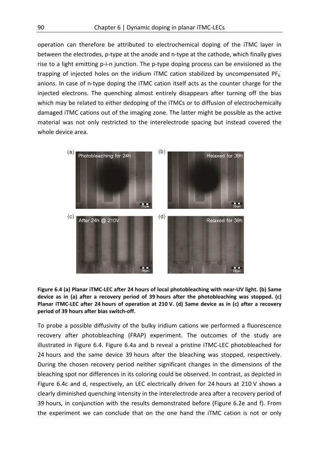
90 Chapter 6 | Dynamic doping in planar iTMC‐LECs
operation can therefore be attributed to electrochemical doping of the iTMC layer in
between the electrodes, p‐type at the anode and n‐type at the cathode, which finally gives
rise to a light emitting p‐i‐n junction. The p‐type doping process can be envisioned as the
trapping of injected holes on the iridium iTMC cation stabilized by uncompensated PF6‐
anions. In case of n‐type doping the iTMC cation itself acts as the counter charge for the
injected electrons. The quenching almost entirely disappears after turning off the bias
which may be related to either dedoping of the iTMCs or to diffusion of electrochemically
damaged iTMC cations out of the imaging zone. The latter might be possible as the active
material was not only restricted to the interelectrode spacing but instead covered the
whole device area.
Figure 6.4 (a) Planar iTMC‐LEC after 24 hours of local photobleaching with near‐UV light. (b) Same device as in (a) after a recovery period of 39 hours after the photobleaching was stopped. (c) Planar iTMC‐LEC after 24 hours of operation at 210 V. (d) Same device as in (c) after a recovery period of 39 hours after bias switch‐off.
To probe a possible diffusivity of the bulky iridium cations we performed a fluorescence
recovery after photobleaching (FRAP) experiment. The outcomes of the study are
illustrated in Figure 6.4. Figure 6.4a and b reveal a pristine iTMC‐LEC photobleached for
24 hours and the same device 39 hours after the bleaching was stopped, respectively.
During the chosen recovery period neither significant changes in the dimensions of the
bleaching spot nor differences in its coloring could be observed. In contrast, as depicted in
Figure 6.4c and d, respectively, an LEC electrically driven for 24 hours at 210 V shows a
clearly diminished quenching intensity in the interelectrode area after a recovery period of
39 hours, in conjunction with the results demonstrated before (Figure 6.2e and f). From
the experiment we can conclude that on the one hand the iTMC cation is not or only

Charge and ion dynamics in light‐emitting electrochemical cells 91
marginally mobile and on the other hand that the PL recovery of the electrically operated
LEC is due to the dedoping of the iTMCs. The PL quenching is nearly completely reversible
after an extended recovery period (Figure 6.2f) indicating that virtually no permanent
degradation occurred during the time frame of these analyses.
As the position of the narrow electroluminescent zone within the interelectrode spacing is
related to the dimensions of the p‐ and n‐type doped regions, their fractions with respect
to the total interelectrode area were calculated as a function of operation time by means
of image processing and the results are included in Figure 6.3. Note that the first
calculations could not be run before the onset of clearly visible light emission after
18 minutes, as the emission line served as the border for the determination of the doped
regions. Moreover, due to its jagged shape, the emission line captures a quite large
fraction of the interelectrode spacing of 5‐10 %. The outcomes of the calculations in Figure
6.3 clearly demonstrate a large extent of p‐type doping (> 70 %) during the early stages of
operation and only a small fraction of n‐type doping (< 20 %). During the subsequent
operation the p‐type doped region is gradually consumed by the n‐type doped region. A
description of this process can be found in the literature.19 N‐type doping becomes
dominant after around 400 minutes and covers more than 55 % of the entire
interelectrode area in the end of operation after 1000 minutes. The results are in accord
with the emission line forming at the cathode and moving towards the anode and
highlight the prerequisite for a migration of the emission zone in LECs: the consumption of
one kind of doping by the other.
6.3.2 ScanningKelvinprobemicroscopyIn addition to the PL experiments we performed scanning Kelvin probe microscopy (SKPM)
to study the transient behavior of the electrostatic potential in the planar iTMC‐LEC. The
outcomes are plotted in Figure 6.5. Due to restrictions in the measurement setup the
maximum voltage that could be applied to the LEC was limited to 100 V. As this voltage
was not sufficient to observe light emission in a device with 10 µm interelectrode spacing,
we used IDEs with a smaller gap size of 5 µm for these investigations. This electrode
spacing can also be clearly deduced from the height profile which is depicted in Figure
6.5a. For clarity the anode and cathode edges are labeled correspondingly. The height
scan was recorded along the horizontal dashed blue line denoted in the AFM topography
image which is displayed as the top inset in Figure 6.5a. This line also corresponds to the
scan direction for the measurement of the potential profiles during operation which are
also included in Figure 6.5a. The arrow denotes the temporal evolution of the electrostatic
potential within a time interval of roughly 4.5 hours. The reason not to use a 5 µm device
as well for the fluorescence microscopy investigations in the previous section is that this
would have led to substantial losses in the image resolution due to the smaller dimensions
of the device structure.

92 Chapter 6 | Dynamic doping in planar iTMC‐LECs
Figure 6.5 (a) Height and transient potential profiles during operation of an iTMC‐LEC. The inset shows AFM images of the topography (top) and the potential map (bottom). The dashed lines indicate the orientation of the profiles with respect to the electrodes and the arrow denotes the temporal evolution of the potential. (b) Complete potential profile across the LEC biased at 52 V. The arrows indicate the measurement window of the profiles shown in (a).
The first SKPM measurement was performed immediately after applying a bias of 100 V to
the iTMC‐LEC at which a sharp potential drop is registered in the middle of the
interelectrode gap. During the subsequent 30 minutes of operation the potential drop
shifts towards the cathodic interface whereas with prolonged operation it moves in the
opposite direction and is displaced towards the anode by the end of the device operation.
For visualization purposes a topography and potential map recorded during the later
stages of operation are shown in the bottom part of the inset in Figure 6.5a. The present
findings are in full agreement with the ECD11‐15 especially with regard to recent SKPM
studies on planar pLECs13, 20‐21 and provide clear evidence for the formation of a p‐i‐n
junction in iTMC‐LECs. The ED which predicts potential drops to occur only at the
electrode interfaces,1, 22‐24 can be ruled out. Our results demonstrate that during the entire
SKPM analysis the potential drop occurs within the interelectrode gap far away from the
contacts. This implies the existence of a high‐ohmic intrinsic region where the large
electric field has to compensate for the low conductivity. Moreover, the intrinsic area is
not fixed to a specific position in between the electrodes but migrates with time as
visualized by the shift of the potential drop.
Even though devices with two different interelectrode spacings have been used, the
results of the SKPM and fluorescence microscopy study are in excellent agreement. The
initially centered drop of the electrostatic potential implies that p‐ and n‐type doping set
in immediately. Note that in the fluorescence microscopy experiments no EL could be
detected in the first 15 minutes. This is probably related to a relatively low doping density.
As the doping density continuously increases, the EL increases until at some moment it is
large enough to be observed. The shift of the potential drop in the SKPM experiments is in
accordance with the fluorescence investigations. Such shifts may be related to imbalances
0 40 80-30
-20
-10
0
10
20
30
Vanode
= 28V
Vcathode
= -24V
Pot
entia
l (V
)
Position (µm)
Potential
Measurement window
0
50
100
150
Height
Heig
ht (
nm
)
0 2 4 6 8 10-30
-20
-10
0
10
20
30 Potential
P
ote
ntia
l (V
)
Position (µm)
-100
-50
0
50 Height
Heig
ht (
nm
)
(a) (b)

Charge and ion dynamics in light‐emitting electrochemical cells 93
in carrier injection, conductivity, doping speed or a combination of these. We note that
even though a voltage of 100 V has been applied to operate the planar iTMC‐LEC, a large
portion of the potential is screened from the interelectrode spacing and drops on top of
the electrodes (see Figure 6.5a). This screening as well as the PL quenching observed on
top of the cathode (see Figure 6.2d and e) indicates that doping also takes place atop the
electrodes. The absence of quenching on top of the anode may be due to a difference in
quenching cross‐sections or doping density.
As the length of the previous potential scans was limited and did not involve the entire
electrodes’ width, we performed a larger‐area scan in a separate SKPM measurement to
record the complete potential profile across the LEC. To allow for a stable SKPM
measurement with reliable results, the maximum voltage that could be applied to the LEC
was limited to below 60 V and we chose a voltage of 52 V. The outcome of the experiment
is illustrated in Figure 6.5b which, for comparison, also shows the measurement window
for the recording of the potential profiles in the initial study. Again a large drop of the
electrostatic potential is observed in the interelectrode gap and also atop both electrodes.
Moreover, the full applied potential is visible which separates into 28 V in the anodic
region and ‐24 V in the cathodic region. A rough estimate of the potential drop in the
interelectrode gap yields a value of 25 V which implicates large potential drops of more
than 10 V atop each electrode. The large potential screening from the gap may be related
to the presence of EDLs that consume more potential than one would expect from the size
of the injection barriers: 0.3 and 2.3 eV (see Figure 6.1c).
To check this, numerical simulations were performed of a 2D representation of the LEC
with buried contacts as shown in Figure 6.6a. The potential map of the simulation in
steady‐state is shown in Figure 6.6b. In Figure 6.6c a side view of Figure 6.6b is shown for
clarity. A clear p‐i‐n junction is visible in between the electrodes, where the slope of the
potential is steepest. Similar to the experiments shown in Figure 6.5 a large part of the
potential drops over the doped regions. Also electric double layers are observed in the
channel and on top of the electrodes, indicated by the large potential drop surrounding
the contacts (see black line in Figure 6.6c). The potential drop over the EDLs is much larger
than the injection barriers of 0.7 eV. In the simulations, the enhanced carrier injection on
top of the electrodes also results in electrochemical doping. Experimentally this is
observed as quenching of the PL on top of the cathode (see Figure 6.2d and e). This
indicates that the geometry of the device may play a role in carrier transport and, related
to this, in the positions of the doped regions as well as of the p‐i‐n junction. The dashed
line in Figure 6.6c represents the potential profile at the interface between the vacuum
and the iTMC layer. This is the interface that would be probed by SKPM. Here the
potential drop over the EDLs (black line) is not observed which is in agreement with Figure

94 Chapter 6 | Dynamic doping in planar iTMC‐LECs
6.5 where buried electrodes were used. Using top electrodes instead, the existence of
EDLs has already been experimentally confirmed in pLECs.20‐21
To summarize the numerical modeling, we prove that it is possible to have a p‐i‐n junction
in combination with large, i.e. exceeding the bandgap, EDLs, provided injection is partially
frustrated. The resultant operation can be viewed as a combination of the ED and ECD
model. This means that in this specific device, device operation is not independent on
electrode material. We should stress that non‐frustrated injection gives rise to purely ECD
behavior.20
Figure 6.6 (a) Schematic of the simulated planar LEC device. (b,c) Steady state result of the simulation of a planar iTMC‐LEC. The dashed line in (c) is taken at the vacuum‐iTMC interface shown in (a) and the thick line in (c) is taken at x = 0, i.e. at the bottom of (a).
A remaining issue is the extremely large bias voltage of 100 V needed to operate the iTMC‐LECs. Similar bias voltages have been used in pLECs with millimeter‐sized gaps.14
Later the voltage was reduced by operation above the melting temperature of the
electrolyte25 or by a different choice of electrolyte.26 The device physics was, however, not
affected. In all cases a thin recombination zone positioned in between two oppositely
doped regions was observed. Here, the use of relatively large bias voltages was necessary
to reduce the turn‐on time as well as to obtain detectable light emission. The generally
low turn‐on time of iTMC‐LECs in comparison to pLECs seems to be related to pronounced
differences in the ionic conductivities, a topic which is addressed in a very recent
publication.27
0100020003000400050000
10
20
30
40
50
60
70
80
90
100
y (nm)
Pot
entia
l (V
)
(a)
(b) (c)
Vacuum
Ionic Transition Metal Complex
2 µm
Anode Cathode
Interface layer
0500
1000
0100020003000400050000
20
40
60
80
100
x (nm)
y (nm)
Pot
entia
l (V
)
150 nm
xy

Charge and ion dynamics in light‐emitting electrochemical cells 95
Finally, based on the present findings and the literature results, a few differences can be
distinguished between planar polymer and iTMC‐LECs. First of all relatively large potential
drops over the EDLs seem to be present in the Ir‐iTMC LEC in contrast to pLECs where
these drops equal the injection barriers.20‐21 This may be related to the sensitivity of LEC
operation on the electrode contacts as previously addressed. For example injection
limitation was demonstrated to result in a device behavior according to the ED whereas
the ECD holds when charge injection is non‐limited.20 In general the electrode work
function was shown to affect charge carrier injection and doping in LECs.16, 28 Moreover, in
the doped regions of iTMC‐LECs large potential drops are identified (Figure 6.5), whereas
in pLECs based on MDMO‐PPV this is typically not the case.20 However, in LECs based on
MEH‐PPV relatively large electric fields are detected in the n‐doped region.13, 17 This
indicates a compensation of dissimilarities between the carrier conductivity in the doped
and undoped regions by the electric field distribution. A similarly large field seems to be
needed in both doped regions in the iTMC‐LEC (Figure 6.4a), which spans a gap of 5 µm.
Hence, these devices still deviate from the idealized LEC in that they are still sensitive to
the interelectrode distance and, related to that, are too resistive to be operated at
relatively low bias voltages. The operational mechanism, however, remains the same:
electrochemical doping enables enhanced carrier injection and transport, while the
applied field redistributes to maximize the overall current passing through.
6.4 ConclusionsBy a combination of fluorescence and scanning Kelvin probe microscopy insight is gained
in the operational mechanism of planar ionic transition metal complex‐based light‐
emitting electrochemical cells. Quenching of the photoluminescence in the interelectrode
gap and a sharp drop in the electrostatic potential far away from the electrodes confirm
an electrochemical doping mechanism which results in the formation of a light‐emitting p‐
i‐n junction. The intrinsic region, where light emission occurs, is not fixed but migrates
with time which might be related to a change in the conductivity of electrons and holes.
The results provide a fundamental basis for a better understanding of iTMC‐based LEC
devices and additionally demonstrate an important challenge: an emission zone centered
and fixated in the middle of the interelectrode spacing immediately at the beginning of
operation to allow for stable and efficient light‐emission.

96 Chapter 6 | Dynamic doping in planar iTMC‐LECs
References
[1] J. D. Slinker, J. A. DeFranco, M. J. Jaquith, W. R. Silveira, Y. W. Zhong, J. M. Moran‐Mirabal, H. G.
Craighead, H. D. Abruna, J. A. Marohn, et al., Nat. Mater. 6 (2007) 894.
[2] D. Tordera, S. Meier, M. Lenes, R. D. Costa, E. Orti, W. Sarfert, H. J. Bolink, Adv. Mater. 24 (2012) 897.
[3] M. Buda, G. Kalyuzhny, A. J. Bard, J. Am. Chem. Soc. 124 (2002) 6090.
[4] H. Rudmann, S. Shimada, M. F. Rubner, J. Appl. Phys. 94 (2003) 115.
[5] M. Lenes, G. Garcia‐Belmonte, D. Tordera, A. Pertegas, J. Bisquert, H. J. Bolink, Adv. Funct. Mater. 21
(2011) 1581.
[6] S. B. Meier, D. Hartmann, D. Tordera, H. J. Bolink, A. Winnacker, W. Sarfert, Phys. Chem. Chem. Phys.
14 (2012) 10886.
[7] H. J. Bolink, E. Coronado, R. D. Costa, E. Orti, M. Sessolo, S. Graber, K. Doyle, M. Neuburger, C. E.
Housecroft, et al., Adv. Mater. 20 (2008) 3910.
[8] F. Gartner, D. Cozzula, S. Losse, A. Boddien, G. Anilkumar, H. Junge, T. Schulz, N. Marquet, A.
Spannenberg, et al., Chem. Eur. J. 17 (2011) 6998.
[9] D. J. Milliron, I. G. Hill, C. Shen, A. Kahn, J. Schwartz, J. Appl. Phys. 87 (2000) 572.
[10] S. T. Parker, J. D. Slinker, M. S. Lowry, M. P. Cox, S. Bernhard, G. G. Malliaras, Chem. Mater. 17 (2005)
3187.
[11] Q. B. Pei, G. Yu, C. Zhang, Y. Yang, A. J. Heeger, Science 269 (1995) 1086.
[12] Q. B. Pei, Y. Yang, G. Yu, C. Zhang, A. J. Heeger, J. Am. Chem. Soc. 118 (1996) 3922.
[13] P. Matyba, K. Maturova, M. Kemerink, N. D. Robinson, L. Edman, Nat. Mater. 8 (2009) 672.
[14] J. Gao, J. Dane, Appl. Phys. Lett. 83 (2003) 3027.
[15] J. Gao, J. Dane, Appl. Phys. Lett. 84 (2004) 2778.
[16] D. B. Rodovsky, O. G. Reid, L. S. C. Pingree, D. S. Ginger, ACS Nano 4 (2010) 2673.
[17] Y. F. Hu, J. Gao, J. Am. Chem. Soc. 133 (2011) 2227.
[18] Y. F. Hu, C. Tracy, J. Gao, Appl. Phys. Lett. 88 (2006) 123507.
[19] N. D. Robinson, J. F. Fang, P. Matyba, L. Edman, Phys. Rev. B 78 (2008) 245202.
[20] S. van Reenen, P. Matyba, A. Dzwilewski, R. A. J. Janssen, L. Edman, M. Kemerink, J. Am. Chem. Soc.
132 (2010) 13776.
[21] S. van Reenen, P. Matyba, A. Dzwilewski, R. A. J. Janssen, A. Edman, M. Kemerink, Adv. Funct. Mater.
21 (2011) 1795.
[22] J. C. deMello, N. Tessler, S. C. Graham, R. H. Friend, Phys. Rev. B 57 (1998) 12951.
[23] J. C. deMello, J. J. M. Halls, S. C. Graham, N. Tessler, R. H. Friend, Phys. Rev. Lett. 85 (2000) 421.
[24] J. C. deMello, Phys. Rev. B 66 (2002) 235210.
[25] J. H. Shin, A. Dzwilewski, A. Iwasiewicz, S. Xiao, A. Fransson, G. N. Ankah, L. Edman, Appl. Phys. Lett. 89
(2006) 013509.
[26] J. H. Shin, L. Edman, J. Am. Chem. Soc. 128 (2006) 15568.
[27] S. van Reenen, T. Akatsuka, D. Tordera, M. Kemerink, H. J. Bolink, J. Am. Chem. Soc. 135 (2013) 886.
[28] D. Hohertz, J. Gao, Adv. Mater. 20 (2008) 3298.

*Part of the work presented in this chapter has been published: S. van Reenen, T. Akatsuka, D. Tordera, M. Kemerink, H. J. Bolink, J. Am. Chem. Soc. 135 (2013) 886.
Chapter7 Universaltransientsin
polymer‐andiTMC‐LECs
Two types of light‐emitting electrochemical cells (LECs) are commonly distinguished, the
polymer‐based LEC (pLEC) and the ionic transition metal complex‐based LEC (iTMC‐LEC).
Apart from marked differences in the active layer constituents these LEC types typically
show operational time scales that can differ by many orders of magnitude at room
temperature. Here, we demonstrate that despite these differences pLECs and iTMC‐LECs
show current, light output and efficacy transients that follow a universal shape. Moreover,
we conclude that the turn‐on time of both LEC types is dominated by the ion conductivity
since the turn‐on time exhibits the same activation energy as the ion conductivity in the
off‐state. These results demonstrate that both types of LECs are really two extremes of one
class of electroluminescent devices. They also implicate that no fundamental difference
exists between charge transport in small molecular weight or polymeric mixed ionic and
electronic conductive materials. Additionally, it follows that the ionic conductivity is
responsible for the dynamic properties of devices and systems using them. This likely
extends to mixed ionic and electronic conductive materials used in organic solar cells and
in a variety of biological systems.

98 Chapter 7 | Universal transients in polymer‐ and iTMC‐LECs
7.1 IntroductionDespite the similarity in steady‐state operation between polymer‐ and iTMC‐LECs as
shown in the previous chapters,1‐9 large differences exist in key properties such as lifetime,
turn‐on time, brightness and efficiency. For comparison, state‐of‐the‐art pLECs exhibit
lifetimes of 5600 h at a brightness of >100 cd m‐2.10‐14 iTMC‐LECs have similar lifetimes at
higher brightness (>600 cd m‐2).15‐16 Furthermore iTMC‐LECs consist of triplet emitters that
intrinsically allow for higher quantum efficiencies. Of all the key properties the turn‐on
time shows the largest difference between both types of devices. Biased at 3‐4 V at room
temperature, pLECs typically turn‐on within a second, whereas iridium‐based iTMC‐LECs
frequently need hours.2, 17‐21 These dynamic differences are the main reason that these
two type of LECs are considered as different classes.
Here we report on a comparative study on the transient behavior of stacked LECs based
on either the polymer MDMO‐PPV or the ionic iridium complex bis(2‐phenylpyridine)(2,2‐
bipyridine)iridium(III) hexafluorophosphate, [Ir(ppy)2(bpy)]+ [PF6]
‐. These were studied by
determining the current and luminance transients at different cell temperatures. The
shape of the transients is found to be independent of operating temperature and more
importantly independent of the type of semiconductor used. The turn‐on time however
varied over several orders of magnitude with temperature and could be described by an
Arrhenius‐type activation energy. The same activation energy was found in the thermal
activation of the ion conductivity in the unbiased state: the turn‐on time is inversely
proportional to the ion conductivity. Together these results prove that next to the steady‐
state operation, also the transient behavior of iTMC and polymer LECs are qualitatively the
same. Hence, pLECs and iTMC‐LECs are really one class of electroluminescent devices.
These results also demonstrate that the ionic conductivity is responsible for the dynamic
properties of devices and systems using mixed electronic and ionic materials.
7.2 MaterialandmethodsDevice preparation: For the conjugated polymer in the active layer of our sandwich LECs
poly[2‐methoxy‐5‐(3’,7’‐dimethyloctyloxy)‐p‐phenylene vinylene] (MDMO‐PPV, Mw > 106 g
mol‐1, American Dye Source) was used. Poly(ethylene oxide) (PEO, Mw = 5∙105 g mol‐1,
Aldrich) was used as received. The salt potassium trifluoromethanesulfonate (KCF3SO3, 98
%, Aldrich) was dried at a temperature T = 473 K under vacuum before use. MDMO‐PPV
(10 mg ml‐1) was dissolved in chloroform (> 99 %, anhydrous, Aldrich). PEO and KCF3SO3
were dissolved separately (10 mg ml‐1) in cyclohexanone (> 99 %, anhydrous, Aldrich).
These solutions were mixed together in a weight ratio of PPV:PEO:KCF3SO3 = 1:1.35:0.25.
This stock solution was thereafter stirred on a magnetic hot plate at T = 323 K for 5 h.
Charge and ion dynamics in light‐emitting electrochemical cells 99
Cleaned glass/ITO substrates were spin‐coated with the stock solution (at 800 RPM for 60
s, followed by 1000 RPM for 10 s) after which they were dried at T = 323 K for at least 1 h
on a hot plate. The thickness of the active layer was 230 nm as determined by
profilometry. Al electrodes were deposited by thermal evaporation under high vacuum (p
10‐6 mbar) on top of the spin‐coated films. All of the above mentioned procedures, save
for the cleaning of the substrates, were done in a glove box under N2 atmosphere ([O2] < 1
ppm and [H2O] < 1 ppm) or in an integrated thermal evaporator.
For the iTMCs‐LECs the devices were made as follows. The emitting complex, [Ir(ppy)2
(bpy)]+ [PF6]‐, was synthesized according to methods described previously.22 Indium tin
oxide ITO‐coated glass plates were patterned by conventional photolithography
(www.narajosubstrates.com). The substrates were cleaned by sonication in successively
water‐soap, water, and 2‐propanol baths. After drying, the substrates were placed in an
UV‐ozone cleaner (Jelight 42‐220) for 20 min. An 80 nm layer of PEDOT:PSS (CLEVIOS P VP
AI 4083, aqueous dispersion, 1.3–1.7 % solid content, Heraeus) was spin‐coated on the ITO
glass substrate to improve the reproducibility of the devices and to prevent the formation
of pinholes. Then a 100 nm transparent film of the emitting complex [Ir(ppy)2 (bpy)]+ [PF6]
‐
was spin‐coated from 30 mg mL–1 acetonitrile solution at 1000 RPM for 20 s. Unless stated
otherwise, the ionic liquid (IL) 1‐butyl‐3‐methylimidazolium hexafluorophosphate,
[BMIM]+ [PF6]‐, (> 98.5%, Sigma‐Aldrich) was added in a 4 to 1 molar ratio (iTMC:IL). The
thickness of the films was determined with an Ambios XP‐1 profilometer. After coating the
films the substrates were transferred to an inert atmosphere glovebox (< 1 ppm [O2] and
[H2O], M. Braun). The Al electrode (70 nm) was thermally vacuum‐evaporated using a
shadow mask (< 3∙10–6 mbar) with an Edwards Auto500 evaporator integrated in the
glovebox. The area of the device was 6.5 mm2. The devices were characterized inside the
glovebox.
Electrical characterization: For characterization of the pLECs a Keithley 2636a sourcemeter
was used to drive the devices and measure the current. The brightness was measured
with a luminance meter (LS‐110 Konica‐Minolta). A Solartron 1260 was used to perform
complex admittance measurements on the LECs in the glovebox. Each point (from 10 MHz
to 1 Hz) was measured during an integration time of 1 s. The rms‐value of the AC voltage
was 0.01 V. The temperature of the device was controlled by use of a Peltier element and
the temperature was measured by a thermocouple.
For characterization of the iTMC‐LECs, transients were measured by applying constant
voltages and monitoring the current and luminance by a True Colour Sensor MAZeT
(MTCSiCT Sensor) using a Botest OLT OLED Lifetime‐Test System. The conductance
spectrum was determined by using a fast Fourier transform of the derivative of the
transient current after setting a small step in the voltage (from 0 V to ‐0.5 V to prevent

100 Chapter 7 | Universal transients in polymer‐ and iTMC‐LECs
carrier injection) by monitoring the current flow using a Keithley 2400 sourcemeter via a
Labview controlled custom‐made protocol. The temperature of the device was controlled
by use of a Peltier element and the temperature was measured by a thermocouple.
7.3 ResultsanddiscussionThe layouts of the iTMC‐ and polymer‐based LECs as well as the structural formulae of the
active layer constituents are shown in Figure 7.1a and b. Figure 7.2 shows the typical
transient behaviors of the luminance, current and efficacy in pristine iTMC‐LECs and pLECs
after application of 3.5 V at two different temperatures. In all measurements the
Figure 7.1 Device layout and the structural formulae of the active layer constituents of (a) the iTMC‐LEC and (b) the polymer LEC.
same is observed: current, luminance and efficacy start to increase after which first the
efficacy rolls off followed by the luminance. These typical transients can be rationalized by
electrochemical doping of the active layer assisted by the mobile ions. Initially, upon
application of a bias voltage, ions start moving and form EDLs at the electrode interfaces.
This initiates injection of electrons and holes. Consequently an electron‐hole current arises
that overtakes the ion current in magnitude. These electrons and holes recombine
radiatively before reaching the other electrode. This explains the initial increase of current
and luminance. The initial increase in efficacy results from the decreasing relative
contribution of the ionic current with respect to the electronic current. Additionally it may
be related to a transition from unipolar to bipolar current due to more balanced carrier
injection. After some time the efficacy is observed to reach a maximum. The following
decrease can be related to exciton quenching. This exciton quenching sets in after EDL
formation when the semiconductor is being electrochemically doped: the carrier density
in the doped regions increases and the n‐ and p‐type doped regions grow towards each
other. The high polaron density in the doped regions close to the recombination region
can cause significant exciton‐polaron quenching.23 Furthermore the enhanced
recombination leads to an enhanced triplet exciton density in the iTMC‐LEC. This is likely
accompanied by triplet‐triplet exciton annihilation.23 After extended operation times the
current density reaches a maximum (not shown) followed by a decrease attributed to
irreversible degeneration.10

Charge and ion dynamics in light‐emitting electrochemical cells 101
Figure 7.2 Current, luminance and efficacy transients of (a,c) pristine Ir‐iTMC‐LECs and (b,d) pristine MDMO‐PPV pLECs biased at 3.5 V. The temperature during operation is shown at the top of each graph.
For comparison the transients in Figure 7.2a‐d were all normalized and plotted in one
graph, shown in Figure 7.3. Normalization of the transients was performed by division of
the efficacy and luminance with their respective peak values. The time and current at
which the luminance peaked was used to normalize these quantities respectively. The
good overlap of the transients in Figure 7.3 indicates that all four devices behave
qualitatively the same, despite differences in semiconductor, ion‐type, operational
temperature, turn‐on time and magnitude of current, luminance and efficacy. The
invariance of the shape by temperature in particular indicates that a single process or
property determines the turn‐on behavior of these cells in this temperature range: most
likely thermal activation of the ‘slow’ ions. The fact that the use of different
semiconductors and ions only leads to minor qualitative differences in the transients
further proves that both types of devices operate according to the same operational
model.1‐2, 7, 9 Processes such as ion dissociation and transport, exciton quenching and
electrochemical doping are (anticipated to be) active in both types of LECs. The large
differences in the magnitude of the current, luminance and efficacy can be related to
differences in the type of emitting material and salt used as well as to the ratio in which
they are mixed. For example, the Ir‐iTMC is a phosphorescent emitter, whereas the PPV is
a fluorescent emitter. Furthermore, the doping dependence of the carrier mobility is likely
different which may lead to differences in the thicknesses of the doped and intrinsic
(a) (b)
(c) (d)
0 2 4 6 8 10 12 14 160
20
40
60
80
100
120
iTMC-LEC T = 293 K C
urre
nt d
ensi
ty (
A m
-2)
Time (h)
Current
0
100
200
300
Luminance
Lum
ina
nce
(Cd
m-2)
0
2
4
6
8
10
Efficacy
Effi
cacy
(C
d A
-1)
0 1 20
50
100
150
Cur
rent
den
sity
(A
m-2)
Time (h)
pLEC T = 263 K
0
5
10
Lum
inan
ce (
Cd
m-2)
0.00
0.05
0.10
0.15
Effi
cacy
(C
d A
-1)
0 20 40 60 80 100 120 1400
200
400
600
800
1000
Cu
rren
t de
nsity
(A
m-2)
Time (s)
iTMC-LEC T = 333 K
0
200
400
600
800
1000
Lum
inan
ce (
Cd
m-2)
0
1
2
3
Effi
cacy
(C
d A
-1)
0 20 40 600
500
1000
Cur
ren
t den
sity
(A
m-2)
Time (s)
pLEC T = 303 K
0
25
50
75
100
125
150
175
Lum
inan
ce (
Cd
m-2)
0.00
0.05
0.10
0.15
0.20
0.25
Effi
cacy
(C
d A
-1)

102 Chapter 7 | Universal transients in polymer‐ and iTMC‐LECs
regions and as a consequence in the current density. The maximum efficacy of both types
of LECs was however found to be independent of the operating temperature (see e.g.
supporting information Figures A.2 and A.3 of Ref. 24).
Figure 7.3 Normalized current, luminance and efficacy transients of polymer and iTMC‐LECs at two temperatures each and biased at 3.5 V.
Comparison of Figure 7.2a and b with respectively Figure 7.2c and d shows a strong
temperature dependence of the turn‐on time in both types of LECs: for the iTMC‐LEC the
turn‐on time changes from hours to tens of seconds by an increase of the temperature
from 27 to 60 oC (see Figure 7.2a and c). For the pLEC similar turn‐on times are obtained in
a different temperature range, namely ‐10 to 30 oC (see Figure 7.2b and d).
Figure 7.4 (a) current, luminance and efficacy transients of a Super Yellow/tetrahexylammonium hexafluorophosphate (1:0.1 in weight) LEC biased at 5 V. The normalized characteristics are plotted together with the results from Figure 7.3 in (b).
Similarly shaped turn‐on transients were reported in other LECs. For example in iTMC‐LECs
based on ruthenium with25 and without26 the addition of PEO. Literature on polymer LECs
without PEO is also available. However, no constant voltage turn‐on transients were
0.0 0.2 0.4 0.6 0.8 1.0 1.2 1.40.0
0.2
0.4
0.6
0.8
1.0
1.2
iTMC-LEC and pLEC N
orm
aliz
ed c
urre
nt
Normalized time
Current
0.0
0.2
0.4
0.6
0.8
1.0
Luminance
Nor
mal
ized
lum
inan
ce
0.0
0.2
0.4
0.6
0.8
1.0
Efficacy
Nor
mal
ized
effi
cacy
0.0 0.2 0.4 0.6 0.8 1.0 1.2 1.40.0
0.2
0.4
0.6
0.8
1.0
1.2
iTMC-LEC and pLEC
Nor
mal
ized
cur
rent
Normalized time
Current
0.0
0.2
0.4
0.6
0.8
1.0
Luminance
Nor
mal
ized
lum
inan
ce
0.0
0.2
0.4
0.6
0.8
1.0
Efficacy
Nor
mal
ized
eff
icac
y
0 1 2 3 4 5 60
5
10
15
Cu
rren
t de
nsity
(m
A c
m-2)
Time (h)
pLEC T = 300 K
0
200
400
Lum
ines
cenc
e (
Cd
m-2)
0
2
4
Effi
cacy
(C
d A
-1)
(a) (b)

Charge and ion dynamics in light‐emitting electrochemical cells 103
reported.17‐18 Therefore we prepared similar LECs comprising Super Yellow PPV admixed
with the salt tetrahexylammonium hexafluorophosphate in a 10% weight ratio. The
(normalized) characteristics are shown in Figure 7.4 and can be identified in Figure 7.4b by
the lighter tone. Again similarly shaped turn‐on transients are observed despite a
relatively large turn‐on time in the order of hours, supporting our claim that the
qualitative operation of semiconductor‐electrolyte systems is universal despite potentially
large differences in performance and response times.
Figure 7.5 Arrhenius plots of the inverse maximum efficacy time iTMC‐LECs with and without the ionic liquid BMIM PF6 and an MDMO‐PPV based LEC. The activation energy determined from the fits is 1.03 and 0.78‐0.85 eV for the pLECs and iTMC‐LECs respectively.
The transients shown in Figure 7.2 originate from four different cells, which do show a
variation in performance that is typical for LECs. To study the temperature dependence
more carefully, more measurements were done on a single pLEC and iTMC‐LEC. Again the
temperature had no effect on the shape of the current, luminance and efficacy transients.
When normalized the transients at different temperatures collapse on top of each other.
Therefore the turn‐on time can be quantified by an arbitrary point on the transients. Here
we take the time at which the efficacy reaches a maximum value. The invariance of the
shape of the transients, the temperature independent peak efficacy as well as additional
PL quantum yield experiments on iTMC‐LECs24 indicate that the EL efficacy is roughly
temperature independent. In Figure 7.5 the natural logarithm of the inverse turn‐on time
was plotted against 1000/T. A linear decrease could be observed in both types of devices
hinting at an Arrhenius type activation in this temperature range. The activation energy
was determined to be 0.8 eV for the iTMC‐LEC and 1.0 eV for the pLEC. Arrhenius plots for iTMC‐LECs without ionic liquid gave similar values for the activation energy (0.8 eV) despite an order‐of‐magnitude slower response.
MDMO PPV + PEO + KTf
-12.0
3.0 3.1 3.2 3.3 3.4 3.5 3.6 3.7-12
-10
-8
-6
-4
-2
0
2
4
1A + BMIM PF6
-9.1
-9.9
1A
-ln t e
ff-m
ax
1000/T (1/K)
-9.2

104 Chapter 7 | Universal transients in polymer‐ and iTMC‐LECs
The transient behavior during turn‐on is determined by the slowest charge carriers in the
LECs: the ions. A way to study the transport of the ions is by looking at the ion conductivity
at sub‐bandgap voltages. For the pLECs the temperature dependence of the ion
conductivity was measured by impedance spectroscopy.9 For the iTMC‐LECs step response
experiments were performed because of the relatively slow ionic response.27 Here the
voltage was stepped from 0.0 V to ‐0.5 V. The relatively large size of the step was
necessary to obtain a reasonable signal‐to‐noise ratio. The negative polarity of the voltage
prevents any carrier injection from the electrodes at the used sub‐bandgap voltages. The
Fourier transform of the time derivative of the step response of the conductance S equals
the complex admittance. The real part of the admittance gives the conductance as a
function of frequency.
Typical ion conductivity spectra at different temperatures of the iTMC‐ and pLEC are
shown in Figure 7.6a and b respectively. All spectra contain a conductivity plateau that
spans roughly 2 decades in the frequency range.9 At higher frequencies an increasing
conductivity is observed that can be related to the response of the dielectric. At lower
frequencies a decreasing conductivity is observed related to EDL formation that effectively
decreases the electric field in the bulk. The minimal value of the measured conductance is
10‐10 S m‐1 below which leakage current starts to dominate the experiment. From the
conductivity plateau an estimate of the ion conductivity could be extracted as indicated by
the arrows. These values are plotted in Figure 7.6c against 1000/T. The linear decrease of
the two semi‐log plots hints again at an Arrhenius type activation. Note that the ion
conductivity in the iTMC‐LEC (see Figure 7.6a) at room temperature or below could not be
determined because of the leakage current. Therefore this data point was ignored in the
fitting. The curves were fitted with the same activation energies as extracted from the
activation in turn‐on time in Figure 7.5. This shows that the ion conductivity and turn‐on
time have the same activation energy and thus are likely related. This strongly suggests
that the turn‐on time in both pLECs and iTMC‐LECs is determined by the ionic
conductivity, i.e. the product of ion density and mobility. This process can be accelerated
by e.g. i) increasing the temperature, ii) use of other (smaller) ions, iii) addition of ion‐
solvating materials like PEO17, 25, 28 or iv) increasing the applied bias voltage.

Charge and ion dynamics in light‐emitting electrochemical cells 105
Figure 7.6 Conductivity spectra for (a) an iTMC‐LEC as determined by step response measurements from 0 V to ‐0.5 V and for (b) a pLEC as determined by impedance spectroscopy. (c) Fits of the ion conductivity by σ(T) = σ0e
‐E/kT where the activation energy, E, was chosen equal to the activation energy determined in Figure 7.5. To fit the data the following values of σ0 were used: 1.6∙10
4 S m‐1 and 4.3∙1011 S m‐1 for the iTMC‐LEC and pLEC respectively.
So far the actual value of the determined activation energy has not been discussed. As ion
conductivity is the product of ion density and mobility, its activation may also be split up in
these two components. The activation in ion density is then related to salt dissociation
into ions, the activation in ion mobility can be regarded as activation of viscosity. In
polymer LECs the equilibrium between the ion density ni and salt density ns can be
described by the following expression:9, 29
. (7.1)
fit: E = 1.0 eV experiment: MDMO LEC
3.0 3.1 3.2 3.3 3.4 3.5 3.6 3.710-12
10-11
10-10
10-9
10-8
10-7
10-6
10-5
10-4
Co
ndu
ctiv
ity (
S m
-1)
1000/T (1/K)
fit: E = 0.8 eV experiment: 1A+BMIMPF
6
10-3 10-2 10-1 100 101
10-10
10-9
10-8
Co
ndu
ctiv
ity (
S m
-1)
Frequency (Hz)
1A +BMIM PF6
(V = 0V --> -0.5V)
T (K) 297 303 313 323 333
10-1 100 101 102 103 104 105 10610-9
10-8
10-7
10-6
10-5
10-4
Co
ndu
ctiv
ity (
S m
-1)
Frequency (Hz)
MDMO-PPV LEC at V = 0 VT (K)
273 283 293 303 313 323 333
(a)
(b)
(c)

106 Chapter 7 | Universal transients in polymer‐ and iTMC‐LECs
Here K is the mass action law constant. Es is the binding energy that is generally estimated
to lie between 0.2 to 0.6 eV.9, 29 For this range of binding energies at the used temperature
range, ns can be estimated to be much larger than ni. As the sum of associated and
dissociated salt is constant, the thermal activation of the ion density can be roughly
described by ni exp(Es/2kT). So effectively 0.1 to 0.3 eV of the 1.0 eV obtained in Figure 7.5 arises from the activation in mobile ion density. That means that the ion mobility has
an activation energy of roughly 0.8 eV. The Arrhenius type activation indicates that the ion
conduction can be described by a simple ion hopping model. A barrier of 0.8 eV must be
overcome by the ion to reach an adjacent site. This hopping is then facilitated by the
motion of PEO chains.30 In literature activation energies of 0.9 eV are reported in high molecular weight PEO admixed with LiCF3SO3.
31 These values are comparable with the
energies found in this work. In the iTMC‐LECs the salts are of a different nature as they
consist of the large iTMC cation and a rather small anion. These ions are not very tightly
bound and therefore the dissociation energy is expected to be low. The activation energy
observed for the iTMC‐LECs may therefore be only related to the activation energy of the
ionic mobility. The addition of ionic liquid only decreased the turn‐on time as shown in
Figure 7.5, whereas the activation energy remained more or less the same. This effect
could originate from an increase in the prefactors of the mobility and carrier density.
These prefactors may also explain why a higher activation energy is found in the polymer
LEC, despite having a smaller turn‐on time.
Mixed electronic and ionic conductive materials are used in a variety of systems and
devices, such as organic photovoltaics,32‐33 electrochemical,34 biological and organic
bioelectronic,35‐36 systems and devices. Therefore, the results obtained here can be of use
to establish the dynamic operation of these devices.
7.4 ConclusionsDespite large quantitative differences, the transient behavior of iTMC‐LECs and pLECs
after switch‐on is shown to be qualitatively equal. This further confirms the identical
operational behavior in both types of LECs. The qualitative transients are independent on
semiconductor‐ and ion‐type and also on the temperature. The thermal activation of both
the turn‐on time and the ion conductivity in the unbiased state were found to be
proportional and could be described by Arrhenius‐type activation with an activation
energy of 0.8‐1.0 eV. These results clearly demonstrate that pLECs and iTMC‐LECs are
really behaving as one class of device.
Charge and ion dynamics in light‐emitting electrochemical cells 107
References
[1] P. Matyba, K. Maturova, M. Kemerink, N. D. Robinson, L. Edman, Nat. Mater. 8 (2009) 672.
[2] M. Lenes, G. Garcia‐Belmonte, D. Tordera, A. Pertegas, J. Bisquert, H. J. Bolink, Adv. Funct. Mater. 21
(2011) 1581.
[3] S. van Reenen, P. Matyba, A. Dzwilewski, R. A. J. Janssen, L. Edman, M. Kemerink, J. Am. Chem. Soc.
132 (2010) 13776.
[4] S. B. Meier, D. Hartmann, D. Tordera, H. J. Bolink, A. Winnacker, W. Sarfert, Phys. Chem. Chem. Phys.
14 (2012) 10886.
[5] A. Munar, A. Sandstrom, S. Tang, L. Edman, Adv. Funct. Mater. 22 (2012) 1511.
[6] T. J. Mills, M. C. Lonergan, Phys. Rev. B 85 (2012) 035203.
[7] S. B. Meier, S. Van Reenen, B. Lefevre, D. Hartmann, H. J. Bolink, A. Winnacker, W. Sarfert, M.
Kemerink, Adv. Funct. Mater. 23 (2013) 3531.
[8] D. B. Rodovsky, O. G. Reid, L. S. C. Pingree, D. S. Ginger, ACS Nano 4 (2010) 2673.
[9] S. van Reenen, R. A. J. Janssen, M. Kemerink, Adv. Funct. Mater. 22 (2012) 4547.
[10] A. Asadpoordarvish, A. Sandstrom, S. Tang, J. Granstrom, L. Edman, Appl. Phys. Lett. 100 (2012)
193508.
[11] J. F. Fang, P. Matyba, L. Edman, Adv. Funct. Mater. 19 (2009) 2671.
[12] L. Edman, S. Tang, J. Phys. Chem. Lett. 1 (2010) 2727.
[13] A. Sandstrom, P. Matyba, L. Edman, Appl. Phys. Lett. 96 (2010) 053303.
[14] Z. Yu, M. Wang, G. Lei, J. Liu, L. Li, Q. Pei, J. Phys. Chem. Lett. 2 (2011) 6.
[15] D. Tordera, S. Meier, M. Lenes, R. D. Costa, E. Orti, W. Sarfert, H. J. Bolink, Adv. Mater. 24 (2012) 897.
[16] D. Tordera, M. Delgado, E. Orti, H. J. Bolink, J. Frey, M. K. Nazeeruddin, E. Baranoff, Chem. Mater. 24
(2012) 1896.
[17] Y. Shao, G. C. Bazan, A. J. Heeger, Adv. Mater. 19 (2007) 365.
[18] B. Gautier, J. Gao, Appl. Phys. Lett. 101 (2012) 093302.
[19] R. D. Costa, E. Orti, H. J. Bolink, F. Monti, G. Accorsi, N. Armaroli, Angew. Chem. Int. Ed. 51 (2012)
8178.
[20] C. V. Hoven, H. P. Wang, M. Elbing, L. Garner, D. Winkelhaus, G. C. Bazan, Nat. Mater. 9 (2010) 249.
[21] I. V. Kosilkin, M. S. Martens, M. P. Murphy, J. M. Leger, Chem. Mater. 22 (2010) 4838.
[22] R. D. Costa, E. Orti, H. J. Bolink, S. Graber, S. Schaffner, M. Neuburger, C. E. Housecroft, E. C.
Constable, Adv. Funct. Mater. 19 (2009) 3456.
[23] M. A. Baldo, R. J. Holmes, S. R. Forrest, Phys. Rev. B 66 (2002) 035321.
[24] S. van Reenen, T. Akatsuka, D. Tordera, M. Kemerink, H. J. Bolink, J. Am. Chem. Soc. 135 (2013) 886.
[25] C. H. Lyons, E. D. Abbas, J. K. Lee, M. F. Rubner, J. Am. Chem. Soc. 120 (1998) 12100.
[26] H. J. Bolink, L. Cappelli, E. Coronado, M. Gratzel, E. Orti, R. D. Costa, P. M. Viruela, M. K. Nazeeruddin,
J. Am. Chem. Soc. 128 (2006) 14786.
[27] D. D. Macdonald, Electrochim. Acta 51 (2006) 1376.
[28] Q. B. Pei, G. Yu, C. Zhang, Y. Yang, A. J. Heeger, Science 269 (1995) 1086.
[29] D. L. Smith, J. Appl. Phys. 81 (1997) 2869.
[30] M. S. Mendolia, G. C. Farrington, Chem. Mater. 5 (1993) 174.
[31] C. J. Leo, G. V. S. Rao, B. V. R. Chowdari, Solid State Ionics 148 (2002) 159.
[32] R. Hany, B. Fan, F. A. de Castro, J. Heier, W. Kylberg, F. Nuesch, Progress in Photovoltaics 19 (2011)
851.

108 Chapter 7 | Universal transients in polymer‐ and iTMC‐LECs
[33] M. S. Su, H. C. Su, C. Y. Kuo, Y. R. Zhou, K. H. Wei, J. Mater. Chem. 21 (2011) 6217.
[34] S. Kim, S. Yamaguchi, J. A. Elliot, MRS Bull. 34 (2009) 900.
[35] R. M. Owens, G. G. Malliaras, MRS Bull. 35 (2010) 449.
[36] M. Berggren, A. Richter‐Dahlfors, Adv. Mater. 19 (2007) 3201.

*Part of the work presented in this chapter has been published: S. van Reenen, M. V. Vitorino, S. C. J. Meskers, R. A. J. Janssen, M. Kemerink, Phys. Rev. B 89 (2014) 205206.
Chapter8 Photoluminescence
quenchingbyelectrochemicaldoping
An important loss mechanism in organic electroluminescent devices is exciton quenching
by polarons. Gradual electrochemical doping of various conjugated polymer films was
studied here to determine the doping density dependence of photoluminescence
quenching. Electrochemical doping was achieved by contacting the film with a solid
electrochemical gate and an injecting contact. A sharp reduction in photoluminescence
was observed for doping densities between 1∙1024 and 2∙1025 m‐3. The doping density
dependence is quantitatively modeled by exciton diffusion in a homogeneous density of
polarons followed by either Förster resonance energy transfer or charge transfer. Both
mechanisms need to be considered to describe polaron‐induced exciton quenching. Thus,
to reduce exciton‐polaron quenching in organic optoelectronic devices, both mechanisms
must be prevented by reducing the exciton diffusion, the spectral overlap, the doping
density, or a combination thereof.

110 Chapter 8 | Photoluminescence quenching by electrochemical doping
8.1 IntroductionOptimization of the external quantum efficiency (EQE) for charge to emitted photon
conversion is presently one of the major challenges in improving organic light‐emitting
devices. At high luminance levels the efficiency typically rolls off due to exciton
quenching.1 Excitons are electron‐hole pairs with a luminescent lifetime dependent on the
type of semiconductor and spin state that can be either a singlet or triplet. They are either
formed by the absorption of a photon or by the meeting of injected electrons and holes.
Excitons can be quenched in the presence of sufficiently large electric fields,2 by other
excitons3 or by polarons4. Which of these is dominant depends on the device and the
emitter used.
Exciton quenching by polarons typically occurs in devices in which high carrier densities
are present close to the region where excitons are formed. Devices with such high carrier
densities are not only light‐emitting electrochemical cells (LECs),5 but also light‐emitting
field‐effect transistors (LEFETs)6 or organic electrochemical light‐emitting transistors
(OECTs).7 In organic light‐emitting diodes (OLEDs), exciton‐polaron quenching becomes
significant at high brightness, necessary for lighting and display applications.1 Also in
organic photovoltaic cells (OPV) exciton quenching is found to be an important loss
process.4 To address this loss process efficiently, it is necessary that the underlying
mechanism is known. In literature attention is mainly given to Förster resonance energy
transfer (FRET) as the main loss mechanism.4, 8‐10 This however does not exclude other
competing loss processes like charge transfer (CT).10‐11
Here we present an experimental study of quenching of optically induced excitons by
polarons introduced by controlled electrochemical doping.12‐13 The doping density was
determined by the integration of the current and confirmed by bleaching of the light‐
emitting polymer. By this method the doping dependence of exciton quenching was
determined for several prototypical conjugated polymers. The doping dependence was
then analytically described by two alternative processes: 1) exciton diffusion followed by
FRET to the polaron associated with the dopant or 2) exciton diffusion followed by CT
between the polaron and the exciton. As both models successfully fit the data, both
processes can account for the observed exciton‐polaron quenching. Doping densities at
which quenching occurs range between 1∙1024 and 2∙1025 m‐3, setting an upper limit for
the doping, or charge density at or near the recombination zone in organic optoelectronic
devices.
8.2 MaterialsandmethodsDevice preparation: The devices in this study consist of a bilayer of a conjugated polymer
and an electrolyte sandwiched between an indium tin oxide (ITO) and a Au electrode. A

Charge and ion dynamics in light‐emitting electrochemical cells 111
schematic of the device is shown in Figure 8.1a. The conjugated polymers are either i)
phenyl‐substituted poly(p‐phenylene vinylene) copolymer (SY‐PPV, Merck, catalogue
number PDY‐132), commonly termed “Super Yellow”, ii) poly[2‐methoxy‐5‐(3',7'‐
dimethyloctyloxy)‐1,4‐phenylenevinylene] (MDMO‐PPV, Mw > 1106 g mol‐1, American
Dye Source) or iii) poly(3‐hexylthiophene) (P3HT, > 98% head to tail, Mn = 54,000–75,000 g
mol−1, Plextronics, purchased from Aldrich). The PPV variants and P3HT were deposited by
first dissolving them in chloroform or chlorobenzene, respectively, to obtain 10 mg ml‐1
solutions, followed by spin coating to yield 100 nm films on top of cleaned ITO
substrates. The electrolyte is a mixture of poly(ethylene oxide) (PEO, Mw = 5x10⁵ g mol‐1,
Aldrich) and potassium triflate (KCF3SO3, 98 %, Aldrich) at a weight ratio of 5:1. The
electrolyte was drop coated from acetone on top of the polymer film, which was placed
on a hotplate at T = 45 oC. The thickness of the solid electrolyte droplet was 2‐3 µm. Gold
electrodes were subsequently thermally deposited in a deposition chamber in a glovebox
under a vacuum of 10‐6 mbar. The thickness of the gold layer was 100 nm. Alternatively,
to enable absorption measurements by transmission, a 30 nm semi‐transparent gold
electrode was used. The active area of the device, defined by a shadow mask, was 0.161
cm2. All device manufacturing was done under nitrogen atmosphere.
Electrical characterization: Current‐voltage characteristics were measured by a Keithley
2400 sourcemeter. For the detection of photoluminescence during electrochemical doping
an Edinburgh time‐resolved fluorescence spectrometer FLS920 was used. For these
measurements the device was put in a closed nitrogen‐filled box with a glass window. For
the detection of the absorption during electrochemical doping, a Shimadzu UV‐1601PC
UV/visible scanning spectrophotometer was used. For these measurements the device
was put in a closed nitrogen‐filled box with two windows to allow for measurements in
transmission. Absorption measurements were also performed by measurement of the
reflection. In this case, a device with a 100 nm gold top electrode was used.
8.3 ExperimentalresultsTo investigate the polaron density dependence of luminescence quenching in conjugated
polymers, a solid‐state electrochemical cell was fabricated as described above. A
schematic of the device layout is shown in Figure 8.1a. The device contains a 100 nm film
of conjugated polymer. On the bottom side this film is contacted by a transparent ITO
electrode to allow for electronic charge carrier injection. The top side of the film is
electrochemically gated to allow ionic charge carrier injection. Dependent on the sign of
the applied bias voltage, the cell was electrochemically n‐type or p‐type doped. Schematic
illustrations of both types of doping are drawn in Figure 8.1b and c. This doping can be
viewed as electrostatic stabilization of injected electronic charges in the conjugated

112 Chapter 8 | Photoluminescence quenching by electrochemical doping
polymer by injected anions or cations. Note, in this context, the strong similarity to the
dynamic doping process occurring in LECs. 14‐15
Figure 8.1 (a) Schematic device layout for electrochemical doping of light‐emitting polymers (LEP). The same schematic after p‐type and n‐type electrochemical doping is shown in (b) and (c) respectively. Dark gray, light gray, white, and black dots represent anions, cations, holes, and electrons, respectively.
To determine the doping density dependence of the exciton quenching in the conjugated
polymer films, two experiments were performed simultaneously: i) the change in the
photoluminescence of the illuminated film was measured and ii) the polymer film was
gradually, electrochemically doped. To confirm that doping of the conjugated polymer
indeed took place, the optical absorption was monitored in an additional experiment.
Figure 8.2 PL‐excitation and PL‐emission spectra of SY‐PPV, MDMO‐PPV, and P3HT. For the PL excitation measurements a detection wavelength of 550 nm was used. For the PL emission measurements an excitation wavelength of 440 nm was used.
Prior to the experiment photoluminescence (PL) excitation and emission spectra were
determined for the different polymer films (Figure 8.2). The wavelengths at which the
spectra show a peak were used as the excitation and emission wavelength during the
transient quenching experiment. To compensate for the background emission an ITO‐
electrolyte‐Au device was prepared and characterized at the same emission and excitation
wavelengths. During the doping experiments, that are explained below, the normalized
(a) (b) (c)
Au
ITO
Glass
PEO+KTf(5:1 in w%)
LEP
+‐ + ‐+ ‐+ ‐+ ‐
+ ‐ +
‐
+
‐
+ ‐
+
‐
+ ‐
+
‐ +
‐
+
‐
+ ‐
+
‐
+ ‐
+
‐
pristine p‐type doped n‐type doped
300 400 500 600 700 800
0.0
0.5
1.0
SY-PPV MDMO-PPV P3HT
PL
exc
itatio
n (
a.u.
)
Wavelength (nm)
0.0
0.5
1.0
PL
emis
sion
(a.
u.)

Charge and ion dynamics in light‐emitting electrochemical cells 113
change in PL was determined as well. In Figure 8.3, it is indicated by the solid line. As the
doping progresses in time, the PL is found to decrease.
Figure 8.3 PL (solid line), applied bias voltage (dashed line), and current (dotted line) transients during p‐type doping of SY‐PPV. The device was excited at λ = 440 nm. PL was detected at λ = 550 nm.
Regarding the doping experiments, a stepwise increasing bias voltage was applied to the
contacts as shown by the dashed line in Figure 8.3. Each bias level was maintained for
approximately 300 s to allow doping to saturate. A typical trace of the current passing
through the cell is indicated on a logarithmic scale by the dotted line in Figure 8.3. After
each bias voltage step, the current is observed to quickly increase, followed by a slow
decrease towards a constant value. This constant value is attributed to leakage and cannot
be related to ongoing electrochemical doping: ions are blocked by the ITO electrode, and
electronic carriers are blocked by the electrolyte, so the electronic current should
ultimately vanish when maintaining a constant bias voltage. This interpretation is
substantiated by the stabilization of the PL quenching signal (light gray line) after each
voltage step on the same time scale as on which the current stabilizes. The fact that the PL
signal does not completely stabilize indicates either a slow redistribution of doping or
ongoing, slow injection of ions into the semiconductor. Leakage currents may be related
to Au diffused into the electrolyte, forming conducting pathways. However, for example in
Ref. 16 we have observed a penetration of Cs into a soft polymer layer by only 15 nm.
The much lower reactivity of Au may, however, increase the penetration depth. By
subtracting the leakage current from the overall current at each bias voltage, the doping
current is determined. Integration of this current with respect to time then gives the
amount of doping put into the 100 nm film. By dividing by the volume of the film the
doping density is obtained. As the leakage current can only be estimated, an error in the
doping density arises which may approximately be a factor 2, as deduced from repetitive
measurements (see supplemental Figure 8.9a in paragraph 8.6).
0 1000 2000 30000.0
0.5
1.0
norm
aliz
ed P
L
Time (s)
PL
10-4
10-3
10-2
10-1
100
101
Current
Cur
rent
(A
)
0
1
2
3
Bias
Bia
s (V
)

114 Chapter 8 | Photoluminescence quenching by electrochemical doping
During doping of the conjugated polymer, the same amount of ions, oppositely charged, is
transported towards the electrolyte‐electrode interface and must be electrostatically
compensated. We assume electric double layer formation of 1 nm at a completely flat
interface would give rise to a significant voltage drop of 3 V,17 which is equal to the maximum applied potential. Clearly this assumption is not correct as a bias voltage of 3 V
is found to be sufficient to dope the organic semiconductor so that a significant bleaching
peak in the absorbance occurs, as is discussed below. The absence of large voltage drops
at the electrolyte‐electrode interface may be related to a large irregular surface area
induced by diffusion of Au into the electrolyte during deposition.16 Furthermore diffusion
of ions through Au during the experiment is also possible, and has been reported before
by Matyba et al.14
Figure 8.4 PL quenching as a function of doping density for SY‐PPV, MDMO PPV, and P3HT.
Combination of the results in Figure 8.3 allowed characterization of the doping density
dependence of the PL quenching process. This was done similarly for n‐ and p‐type doping
of SY‐PPV as well as for p‐type doping of MDMO‐PPV and P3HT. The results are shown in
Figure 8.4. The vertical error bars are related to the PL signal not being stable yet. In each
case a relatively strong decrease in PL emission occurs at doping densities between 1∙1024
and 2∙1025 m‐3, which corresponds to doping levels of approximately 0.1 % and 1.0 % when
assuming a density of states of 1027 m‐3.18 The doping density is determined by integrating
the current after correction for the leakage current. The magnitude of the leakage current
is however uncertain. Therefore the doping density was also calculated without
accounting for the leakage current. The relative contribution of leakage and doping
current (as shown in supplemental Figure 8.9b in paragraph 8.6) shows that the doping
and leakage current increase roughly in parallel. This limits the relative error in the
extracted doping concentration, which is the important quantity in the present discussion.
To quantify the effects of the leakage current, we added corresponding error margins in
Figure 8.4. The indicated upper limit is given by the absolute maximum of possible doping
1022 1023 1024 1025 1026 1027
0.0
0.5
1.0
SY-PPV n-type SY-PPV p-type P3HT p-type MDMO-PPV p-type
Nor
mal
ized
PL
Doping density (m-3)

Charge and ion dynamics in light‐emitting electrochemical cells 115
density in case we correct for no or an underestimated (for P3HT) leakage current. The
data point itself is based on the (over)estimated leakage current and forms therefore a
lower limit. A reference measurement on a cell without organic semiconductor is included
in supplemental Figure 8.10. Neither indications of side‐reactions were observed in the
measured current nor any change in color. More importantly, the leakage currents found
here are approximately an order of magnitude below the currents observed in the full
device, i.e. with the semiconductor present, indicating that the latter is dominated by
doping and not by leakage, in line with our arguments above. In more detail, in
supplemental Figure 8.10 we calculated the associated charge densities by integration of
the leakage currents. The integrated carrier density in the devices with organic
semiconductor is at least larger by an order of magnitude than without the
semiconductor, demonstrating that the extracted doping densities are maximally
overestimated by 10 %.
For accurate determination of the doping density a homogeneous doping distribution is
required. The incomplete stabilization of the PL signal observed in Figure 8.3 indicates that
doping redistributes. Likely, ions are injected in the film in a filamentary or otherwise
inhomogeneous manner, causing strong quenching in those regions. However, the
corresponding density gradients are unstable and a redistribution of ions will follow,
lowering the maximum concentrations and reducing the quenching. The tendency of ions
to redistribute is related to drift and diffusion, both in favor of a homogeneous
distribution. Another, indirect, indication that the doping is relatively homogeneous is the
abrupt reduction of PL versus doping density as shown in Figure 8.4 for SY‐PPV.
Inhomogeneity, i.e. the formation of doped and undoped domains would correspond to a
more gradual reduction of the PL signal. The absence of substantial inhomogeneity is
finally substantiated by optical inspection of the device darkening during doping, which
was found to be homogeneous within the experimental resolution of 102 µm.
Comparison between p‐ and n‐type doping in SY‐PPV demonstrates that p‐type doping
quenches at lower carrier densities. This is in line with observations in planar LECs. In such
cells both types of doping are present simultaneously. The n‐type doped regions of PPV
are typically observed to quench less than the p‐type doping regions.15 Here, we show that
this behavior can at least partially be explained by stronger PL quenching by p‐type
doping. A comparison between P3HT and MDMO‐PPV shows only small differences in
shape and critical doping density of PL quenching by p‐type doping. N‐type doping in
MDMO‐PPV and P3HT occurred at relatively large bias voltages at which electrochemical
reactions with the electrolyte distort the measurements. Therefore, these measurements
were not included. The functional shape of the quenching curve of P3HT and MDMO‐PPV
seems to be different from that of SY‐PPV. We return to this at the end of the discussion
section.

116 Chapter 8 | Photoluminescence quenching by electrochemical doping
Figure 8.5 Absorbance of (a) p‐ and (b) n‐type doping in SY‐PPV at different doping levels. The absorbance by doping is determined by subtracting the absorbance at any bias voltage by the absorbance of the unbiased cell: Adoping = A(Vbias) – A(Vbias = 0). A semi‐transparent Au top electrode was used with a thickness of 30 nm. The black arrows indicate the change in absorbance for larger doping densities, starting at zero doping. The insets show the normalized PL (gray dashed) and the absorbance (black solid) by doping as a function of applied bias.
Next to the effect of PL quenching induced by doping, the absorption spectrum of the
dopants was also measured in SY‐PPV. The change in absorbance by doping of SY‐PPV is
plotted in Figure 8.5(a) and (b) for p‐ and n‐type doping, respectively. The negative
differential absorbance at λ = 460 nm is at the same position as the absorption spectrum
of SY‐PPV (dotted light gray line in Figure 8.2). The effect is therefore related to bleaching:
doping fills the density of states, reducing the number of sites available for the formation
of excitons.12 This bleaching is an important observation as it indicates filling of the density
of states of the light‐emitting polymer. The enhanced transmission due to ground state
bleaching of ΔT/T 2.1 (see Figure 8.5(a); the trace where a bleaching peak at λ = 460 nm
is observed of A = ‐0.5, where ΔT/T = 10‐A‐1) was measured at an electrically determined
charge density between 5∙1026 and 3∙1027 m‐3. To estimate whether these values are
reasonable, we made a comparison with values obtained from Ref. 19‐20, where a relative
enhancement in transmission by 6∙10‐4 was observed at a (photoexcited) charge density of
1∙1024 m‐3. Making the reasonable assumption that bleaching is linear in density, densities
of 5∙1026 and 3∙1027 m‐3 would then lead to ΔT/T between 0.3 and 1.8, respectively. This
value is in more than reasonable agreement with the ΔT/T 2.1 we measure, especially
since we ignore differences, for example in site density, between the materials. This
confirms that electrochemical doping of the conjugated polymer indeed takes place and
that the calculated doping density by the integration of the current is reliable.
To determine whether the PL quenching in Figure 8.4 originates from the reduced optical
density as observed in Figure 8.5, the relative absorbance and the normalized PL are
plotted in the same graph in the insets in Figure 8.5a and b. For both p‐ and n‐type doping
(a) (b)
400 500 600 700 800-0.8
-0.6
-0.4
-0.2
0.0
A
bso
rban
ce
wavelength (nm)
400 500 600 700 800-0.8
-0.6
-0.4
-0.2
0.0
Abs
orb
ance
wavelength (nm)
0 1 2 3 4
0.0
0.5
1.0
Nor
mal
ize
d P
L
|Bias voltage| (V)
-0.5
0.0
Ab
sorb
anc
e
0 1 2 3 4
0.0
0.5
1.0
Nor
mal
ize
d P
L
|Bias voltage| (V)
-0.5
0.0
Ab
sorb
anc
e

Charge and ion dynamics in light‐emitting electrochemical cells 117
of SY‐PPV, bleaching sets in clearly after the majority of PL has already been quenched.
Hence PL quenching and absorption bleaching are independent processes in this respect.
At larger wavelengths in Figure 8.5a and b absorption bands appear for both n‐ and p‐type
doping. These bands sit partially at the same wavelength as the PL spectrum of SY‐PPV
(solid light gray line in Figure 8.2) and are attributed to polaron absorption.12
8.4 DiscussionTo interpret the results shown in Figure 8.4, first the effect of applying a bias voltage to
the device (see Figure 8.1a) needs to be understood. Initially, the PEO is filled with ions
whereas the PPV is considered empty. The difference in chemical potential of the ions in
both layers is expected to be strongly in favor of the PEO film due to its chemical
structure. This difference forms an ion injection barrier which impedes ion injection into
the PPV film. This difference across the PEO‐PPV interface is however opposed by i) a
difference in ion density resulting in an ion diffusion current and ii) a difference in
electrostatic potential due to the bias voltage applied to the contacts. Increasing the
applied bias voltage results in an increased ion density at the interface, enlarging both the
potential drop and the density gradient at the interface. This, in turn, drives ions into the
semiconductor. In the experiment the bias voltage is increased stepwise and ion injection
is observed at sufficiently large voltages. K+ or CF3SO3‐ injection in SY‐PPV are observed to
start at |Vbias| 1.6 V and 1.2 V for n‐ and p‐type doping, respectively, see insets in Figure 8.5a and b.
The exciton quenching process in Figure 8.4 is the result of an interaction between a
polaron, stabilized by an ionic dopant, and an exciton. No significant external electric field,
which could also contribute to exciton quenching, is expected within the SY‐PPV layer: the
boundary conditions induced by the electrode and the electrolyte result in a
homogeneous pile‐up of ionic and electronic carriers in the SY‐PPV film. Once injected by,
respectively, the electrolyte or the electrode, the carrier cannot leave the film through the
other contact. This means that ultimately the net electronic and ionic current must be
zero. The net current is determined by drift and diffusion, which should thus cancel or
both be equal to zero. As the doping mechanism leads to electronic and ionic carriers
having the same density profile, diffusion is in the same direction for both types of
carriers. Drift, however, is in opposite directions for both types of carriers due to the
difference in charge. Hence, to obtain a zero net electronic and ionic current the drift and
diffusion components of the ionic dopants and the polarons must both be zero. The zero
diffusion current implies that constant concentrations for electronic and ionic carriers are
present. These qualitative arguments are confirmed by numerical drift‐diffusion
simulations shown in supplemental Figure 8.11.

118 Chapter 8 | Photoluminescence quenching by electrochemical doping
Regarding exciton quenching by polarons, two alternative processes shall be considered:
Förster resonance energy transfer and charge transfer. Other alternatives like multipolar
interactions21 were not considered. Diffusion of the exciton through the film prior to
quenching must, however, be accounted for. Polaron diffusion was found to be negligible
compared to exciton diffusion, as will be justified below in section C. In Figure 8.6 a
schematic representation is given of both models. In the next two paragraphs these
models are discussed in detail and will be related to our experimental findings.
Figure 8.6 Schematic representation of the considered exciton quenching mechanisms in a random distribution of doping sites: (a,c) Förster resonance energy transfer and (b,d) charge transfer. Both mechanisms are preceded by exciton diffusion.
8.4.1 Försterresonanceenergytransfer(FRET)Resonance energy transfer is an energy transfer between a donor and an acceptor.22 In
our case the acceptor is an electron‐ or hole‐polaron that is excited to a higher state, as
illustrated in Figure 8.6a. Since the donor loses its excitation by to the acceptor by the
coupling of transition dipoles it is a non‐radiative loss process. Spectral overlap, however,
is required between the emission spectrum of the donor and the excitation spectrum of
the acceptor to make the process efficient. The spectra in, respectively, Figure 8.2 and
Figure 8.5 show that this is indeed the case in SY‐PPV for exciton emission and polaron
excitation. In the next subsections two possible scenarios for FRET are explained.
++
+ +
1. Diffusion
Charge transferFörster resonanceenergy transfer
+
1. Diffusion +
+
+
+
+
+
2. FRET
(a) (b)
(c) (d)
2. CT
Exciton Polaron
Diffusion
Exciton Polaron
Charge transfer
Exciton PolaronExciton Polaron
DiffusionFörster resonance energy transfer

Charge and ion dynamics in light‐emitting electrochemical cells 119
8.4.1.1 SinglepairoffixeddipolesThe most basic description of FRET is between a donor and an acceptor that are two
dipoles, fixed in their relative orientation and position. The transfer rate constant derived
by Förster is expressed as
, (8.1)
where is the lifetime of the donor in absence of energy transfer, r is the distance
between donor and acceptor, and is the critical distance at which the probability of
transfer and decay of the donor is equal. The Förster radius can be determined
experimentally and is expressed as
, (8.2)
where is the orientational factor, Φ is the fluorescence quantum yield of the donor
without transfer, n is the average refractive index of the medium, is the normalized
fluorescence spectrum of the donor, and is the molar absorption coefficient of the
acceptor.
In our case, this description of FRET does not apply as the formed exciton is likely to be
mobile and is excited in a film filled with multiple acceptors. Therefore, exciton diffusion
and multiple acceptors need to be taken into account for a correct description.
8.4.1.2 ExcitondiffusionwithmultipleacceptorsThe exciton quenching process can be described by diffusion with a sink term,
⁄ , with the correct distance dependence between the donor and acceptor, r.22‐23 The
donor and acceptor are approximated as point dipoles, i.e. excluding delocalization of the
polaron and exciton. For excitons a delocalization over several monomer subunits may be
expected (e.g. 1 nm24). Polarons compensated by ions at relatively low doping levels of
1% are more localized due to the ionic Coulomb trap (i.e. < 1 nm).13 The diffusion
equation then becomes
,, , , (8.3)
where CE is the exciton density and Dexc the exciton diffusion coefficient. Gösele et al.
found the following approximate solution to this problem:23
4 1 / , (8.4)
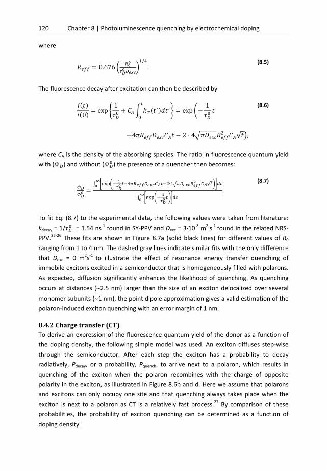
120 Chapter 8 | Photoluminescence quenching by electrochemical doping
where
0.676
/
. (8.5)
The fluorescence decay after excitation can then be described by
0exp
1exp
1
4 2 ∙ 4 2 √ ,
(8.6)
where CA is the density of the absorbing species. The ratio in fluorescence quantum yield
with (Φ ) and without (Φ ) the presence of a quencher then becomes:
∙ √
.
(8.7)
To fit Eq. (8.7) to the experimental data, the following values were taken from literature:
kdecay = 1/ = 1.54 ns‐1 found in SY‐PPV and Dexc = 3∙10‐8 m2 s‐1 found in the related NRS‐
PPV.25‐26 These fits are shown in Figure 8.7a (solid black lines) for different values of R0
ranging from 1 to 4 nm. The dashed gray lines indicate similar fits with the only difference
that Dexc = 0 m2s‐1 to illustrate the effect of resonance energy transfer quenching of
immobile excitons excited in a semiconductor that is homogeneously filled with polarons.
As expected, diffusion significantly enhances the likelihood of quenching. As quenching
occurs at distances (2.5 nm) larger than the size of an exciton delocalized over several
monomer subunits (1 nm), the point dipole approximation gives a valid estimation of the
polaron‐induced exciton quenching with an error margin of 1 nm.
8.4.2 Chargetransfer(CT)To derive an expression of the fluorescence quantum yield of the donor as a function of
the doping density, the following simple model was used. An exciton diffuses step‐wise
through the semiconductor. After each step the exciton has a probability to decay
radiatively, Pdecay, or a probability, Pquench, to arrive next to a polaron, which results in
quenching of the exciton when the polaron recombines with the charge of opposite
polarity in the exciton, as illustrated in Figure 8.6b and d. Here we assume that polarons
and excitons can only occupy one site and that quenching always takes place when the
exciton is next to a polaron as CT is a relatively fast process.27 By comparison of these
probabilities, the probability of exciton quenching can be determined as a function of
doping density.

Charge and ion dynamics in light‐emitting electrochemical cells 121
The exciton quenching probability after one diffusion step can be related to the ratio of
doped site density ndoping and the density of states nDOS:
, (8.8)
where A is the average number of new neighboring sites that can quench the exciton. The
value of A depends on the coordination of the excitons and polarons. In the first instance,
a one‐dimensional system is assumed for the polymer system. To determine the
quenching probability as a function of doping density, nDOS = 6∙1026 m‐3 and A = 2 were
taken.18 Furthermore we assumed ‘physical’ contact between exciton and charge is
required for quenching and nDOS‐1 equals the mean volume of a site –we assume excitons
and polarons sit on sites of equal volume. Clearly, this is a gross simplification as some
tunneling is likely to be relevant to quenching, implying the presence of a spatial gap and
thus a reduced site volume. Here, nDOS‐1 is thus a coarse upper limit to the ‘real’ exciton
and polaron volumes. The used value for nDOS, 6∙1026 m‐3, puts an upper limit just above 1
nm3, consistent with the length scales of a delocalized exciton.24
The radiative decay rate of a single exciton was set to a fixed rate krad,decay. For an
ensemble of excitons this gives rise to an exponential radiative decay with a radiative
decay rate krad,decay when exciton‐exciton interactions are ignored. The time of a single
diffusion step is set equal to the time needed to overcome the distance of one
neighboring site ⁄ by diffusion. The diffusion length r is, in turn, related to the
exciton diffusion constant Dexc as 2 . The radiative decay probability during
this single diffusion step can then be described by
, 1 ,
∙ / . (8.9)
To determine the radiative decay probability, the following values were taken from
literature: krad,decay = 1.54 ns‐1 and Dexc = 3∙10
‐8 m2 s‐1.25‐26
Under the assumption that initial and final sites are independent the
fluorescence quantum yield can then be determined by:
,
,, (8.10)
A fit of this function for the given parameters is shown in Figure 8.7b by the solid black
lines for A = 6, 4, 3, 2 neighbors. The dashed gray lines indicate similar fits with the only
difference that Dexc = 0 m2 s‐1 to illustrate the effect of CT quenching of immobile excitons
excited in a semiconductor that is homogeneously filled with polarons. An alternative

122 Chapter 8 | Photoluminescence quenching by electrochemical doping
approach to determine the effect of CT on the fluorescence quantum yield is by using Eq.
(8.3) with a sink term ~exp ⁄ ,10, 28 which must be solved numerically. An
analytical expression can however be found when solving Eq. 3 for k = 0 and the boundary
condition that the probability of exciton quenching equals 1 when the exciton is inside a
sphere with radius Rc around the acceptor.22 A fit based on this model for ⁄
,
krad,decay = 1.54 ns‐1 and Dexc = 3∙10
‐8 m2 s‐1 gives fits qualitatively similar to the fits based on
Eq. (8.10).25‐26
Figure 8.7 Fits (lines) of the PL quenching data (symbols + shaded region) of n‐type doping of SY‐PPV (down triangles) and p‐type doping of SY‐PPV (up triangles), MDMO‐PPV (squares) and P3HT (dots). (a) Fits following the resonance energy transfer model without diffusion are dashed gray (see Eq. (8.7); Dexc = 0 m
2 s‐1; R0 = 4, 2.5, 1.5, 1.0 nm from left to right) and with diffusion solid black (see Eq. (8.7); Dexc = 3∙10
‐8 m2 s‐1; R0 = 4, 2.5, 1.5, 1.0 nm from left to right). (b) Fits following the charge transfer model without diffusion dashed gray (see Eq. (8.10); Dexc = 0 m
2 s‐1; A = 2, 3, 4, 6 neighbors from left to right) and with diffusion solid black (see Eq. (8.10); Dexc = 3∙10
‐8 m2 s‐1; A = 2, 3, 4, 6 neighbors from left to right).
8.4.3 ComparisonofFRETandCTComparison between the fits related to FRET and CT in Figure 8.7 shows that there is little
qualitative difference in the doping dependence between the two quenching mechanisms.
This demonstrates that instead of the actual quenching model, FRET or CT, the
homogeneous density of quenchers determines the qualitative doping density
dependence of the exciton quenching. In fact it is not at all unlikely that both processes,
CT and FRET, take place simultaneously. Given the fact that the doping density
dependence is slightly different for both models, the relative contributions of both
processes would also be dependent on the doping density. Regarding diffusion, also
polaron diffusion may play a role in exciton quenching. This is however only the case for
high mobility semiconductors like P3HT. The exciton diffusion itself can also be expected
to be doping density dependent. An indication for this is discussed below.
1022 1023 1024 1025 1026 1027
0.0
0.5
1.0
dataFRET
no diffusion diffusionN
orm
aliz
ed
PL
qu
ench
ing
Doping density (m-3)1022 1023 1024 1025 1026 1027
0.0
0.5
1.0
dataCT
no diffusion diffusionN
orm
aliz
ed P
L qu
ench
ing
Doping density (m-3)
(a) (b)

Charge and ion dynamics in light‐emitting electrochemical cells 123
The data that is qualitatively fit by both models is that of the p‐type doping in MDMO‐PPV
and P3HT. The shift towards a lower doping density observed for P3HT can be related to
the larger exciton diffusion coefficient in P3HT:29 1.8∙10‐7 m2 s‐1 compared to 3.2∙10‐8 m2 s‐1
in MDMO‐PPV.30 The exciton lifetime in both materials is similar.31‐32 It should be noted
that given the exciton lifetime and the exciton diffusion coefficients of P3HT and MDMO‐
PPV, a relatively small value of R0 of 1‐1.5 nm is needed to quantitatively fit FRET in
Figure 8.7a. The error in experimentally determined doping density of roughly a factor 2
results in an uncertainty in R0 of 0.5 nm. By measurement of the absorption spectrum in
reflectance of p‐type doping in MDMO‐PPV (see supplemental Figure 8.12a), R0 could be
calculated from Eq. (8.2). To this purpose the emission spectrum as shown in Figure 8.2
was used. The orientation factor κ2 was taken to be 0.65533 and the refractive index n is
estimated to be 2.34 Note that κ2 can possibly range between 0 and 4. In case the donor
and emitter dipole lie in a plane κ2 equals 0.655.22, 33 A fluorescence quantum yield of 8%
was taken from Ref. 35. The resultant R0 for p‐type doping in MDMO‐PPV was found to be
approximately 3.0±0.3 nm. This value is larger than the fitted value of 1.5 nm in Figure
8.7b. However, the factor 2 difference is well within the margins induced by the
uncertainties in the assumed exciton lifetime and diffusion coefficient, in the orientation
factor and in the measured doping density.
The data for SY‐PPV are, on the other hand, not nicely fit by either of the two models, see
Figure 8.7: the PL declines steeply at relatively large doping densities. The onset of PL
quenching at these large doping densities can only be reconciled with the models when
exciton diffusion is excluded (see Figure 8.7a and b for Dexc = 0). Regarding FRET, a R0 of
maximally 2.5 and 1.5 nm would then be required for exciton quenching by p‐ and n‐
type doping, respectively. To address the consistency of this hypothesis, R0 was calculated
from Eq. (8.2), using the emission spectrum of SY‐PPV in Figure 8.2. The molar absorption
coefficients of the n‐ and p‐type polarons were determined by either the absorption
spectra in Figure 8.5 or the absorption spectra measured in reflectance in supplemental
Figure 8.12a. These absorption spectra were taken at known doping densities. The
orientation factor κ2 was again taken to be 0.65533 and the refractive index n to be 2.34 A
fluorescence quantum yield of 17% was taken from Ref. 25. The resultant values of R0 for
p‐ and n‐type doping were 2.8±0.6 nm and 2.3±0.4, respectively. This means that the
rather large p‐type doping density threshold at which PL in SY‐PPV is quenched can indeed
be explained by both the FRET and the CT modeling in case exciton diffusion is somehow
blocked. For n‐type doping an R0 value of 2.3±0.4 nm would suggest a stronger quenching
by FRET than observed in Figure 8.7a, even when diffusion is excluded. However, the
sources of possible errors discussed above for MDMO‐PPV can also in this case very well
lead to this discrepancy.

124 Chapter 8 | Photoluminescence quenching by electrochemical doping
Figure 8.8 (a) Schematic device layout of the electrochemical transistor. (b) Electronic carrier mobility as a function of doping density. Lines were added that serve as guides to the eye to visualize the density threshold after which the mobility is observed to increase significantly.
The sudden drop in PL intensity beyond the onset of quenching may then be related to an
enhancement of the exciton diffusion: in case exciton diffusion in SY‐PPV rapidly increases
around a p‐type doping density of 2∙1024 m‐3, a rapid transition between the dashed gray
line and the solid black line for, as an example, R0 = 2.5 nm is expected in Figure 8.7a. This
would then be in line with the experimentally obtained PL quenching profile for p‐type
doping in SY‐PPV. To substantiate the suggestion of an abrupt increase in exciton diffusion
and to provide a possible physical reason, mobility measurements in n‐ and p‐type doped
SY‐PPV in an electrochemical transistor structure (see Figure 8.8a) were performed. The
results show a threshold for the doping density dependence of the mobility, as plotted in
Fig. 8b. Interestingly, the thresholds for n‐ and p‐type doping in Figure 8.8b coincide quite
well with the densities at which the sudden transitions in Figure 8.7 occur. Note that the
error in experimentally determined doping density is relatively small at these low doping
densities. Also note the coincidence of doping density at which PL quenching is initiated
and at which the mobility is enhanced. This suggests a direct connection between on the
one hand charge mobility and trapping, and on the other hand exciton diffusion.36 Within
the lifetime of the exciton, diffusion by polarons is, however, not significant in SY‐PPV.
From the mobilities in Figure 8.8b and the Einstein relation, a polaron diffusion constant
Dpol between 10‐14 m2 s‐1 and 10‐11 m2 s‐1 can be estimated. These numbers are small
compared to the exciton diffusion constant that is in the range 10‐8 m2 s‐1. Nevertheless,
the relatively weak quenching in SY PPV found here (again) confirms the finding that
electroluminescence from copolymers is relatively strong compared to their homopolymer
counterparts, e.g. MDMO‐PPV.37‐38
In principle the abrupt PL quenching in SY‐PPV could also be related to an erroneous
determination of the doping density. Due to the chemical potential difference at the
PEO:LEP interface, an electric double layer (EDL) is formed by a small (fraction of the)
1022 1023 1024 1025 1026 1027
10-12
10-11
10-10
10-9
10-8
MDMO-PPV p-type
SY-PPV n-type p-type
Mob
ility
(m
2 V-1 s
-1)
Doping density (m-3)
(a) (b)Au
ITO
Glass
PEO+KTf(5:1 in w%)
+‐
+ ‐+ ‐+ ‐+ ‐
+ ‐
LEP

Charge and ion dynamics in light‐emitting electrochemical cells 125
charging current before actual doping sets in. A difference in chemical potential for the
ions in SY‐PPV, MDMO‐PPV and P3HT might then result in the different quenching profiles
as shown in Figure 8.4. A 1 nm sheet electric double layer with a potential drop of 1 V
would then correspond to a surface charge density of 3∙1021 m‐2. Such a charge density
residing in a 1 nm sheet at the interface would correspond to a doping concentration in
the entire film (100 nm) of a factor 100/1 = 100 times lower. Since the biases used in the
experiment are in the 0 V to 3 V range, the amount of doping lost to EDL formation is
negligible in comparison to the total doping concentration. Hence, the anomalous
behavior in SY‐PPV compared to MDMO‐PPV or P3HT cannot be attributed to a difference
in chemical potentials between these materials.
The qualitative behavior of the doping dependence of PL quenching in the experiment and
the models (see Figure 8.7) confirms on hindsight that the experiment is characterized by
homogeneous doping. Successive doping of phase separated regions would lead to a two‐
step reduction of the PL. In case such an effect is more gradual, then quenching would still
be expected to be distributed over a larger total injected charge density (horizontal axis of
Figure 8.7) than in the case of homogeneous doping. The models assume a homogeneous
doping density and are able to model the qualitative behavior relatively well (for P3HT and
MDMO‐PPV). It is in this context important that, for both models, changes in parameter
values have little or no effect on the steepness of the slope; hence, an inhomogeneity‐
induced broadening cannot easily be mapped on (a change in) any of the fitting
parameters. A steeper doping density dependence (for SY‐PPV) is furthermore not in line
with the doping over phase‐separated regions as indicated above. Therefore, combined
with the discussion in the Experimental results section, we do not see any indication that
significant inhomogeneous doping of the conjugated polymer takes place.
The doping densities at which polaron‐induced exciton quenching occurs are relevant
densities for various types of devices. In efficient polymer LECs, salt densities of 6∙1025 m‐
3 are present in the active layer.39 In case all salt dissociates into ions, such salt densities
lead to highly doped regions that can quench all excitons in case they sit close to the
recombination zone. Organic light‐emitting diodes operating in the space charge limited
regime on the other hand generally do not reach the carrier densities found here for
exciton quenching. Only when relatively large bias voltages are used to obtain high
brightness may the polaron density result in significant exciton quenching.1 In light‐
emitting field effect transistors carrier densities in the range 1024‐1026 m‐3 pile up near the
recombination zone. As a result exciton‐polaron quenching may significantly reduce the
efficiency if not prevented by, for example, the introduction of multiple layers to separate
carrier transport from carrier recombination.40 In bulk heterojunction solar cells, polaron
densities around 1022 m‐3 are typically reached under illumination.41 Therefore, in these

126 Chapter 8 | Photoluminescence quenching by electrochemical doping
cells, polaron‐induced exciton quenching is unlikely to lead to a significant reduction in
efficiency.
8.5 ConclusionsThe effect of polaron‐induced exciton quenching in conjugated polymers has been studied
in a solid‐state polymer film. By controlled electrochemical doping the polaron density
dependence of the exciton quenching could be determined in several polymers. The
density was furthermore confirmed by the occurrence of a bleaching peak in the optical
absorption. The critical doping density at which exciton quenching occurs ranges between
1∙1024‐2∙1025 m‐3 , including the experimental uncertainty, setting an upper limit for the
carrier density near and at the recombination zone of efficient emissive devices. The
density dependence itself could be modeled by considering exciton diffusion followed by
either charge transfer or Förster resonance energy transfer in a homogeneous density of
polarons. Both FRET and CT qualitatively fit the data. Fitting with parameters obtained
from literature resulted in reasonable quantitative fits with PL quenching occurring at
similar polaron densities. It shows that for interpreting experimental data related to
polaron‐induced exciton quenching, i) exciton diffusion, ii) charge transfer and iii)
resonance energy transfer should be considered. Thus, to reduce exciton quenching in
devices which convert electrical current in light, the exciton diffusion, the spectral overlap
between the emitting exciton and the absorbing polaron, and/or the polaron density need
to be reduced.
8.6 Supplementalfigures
Figure 8.9 (a) PL quenching as a function of doping density for SY‐PPV. (b) Integrated leakage and doping current, c.f. Figure 8.3. To calculate the integrated leakage and doping current in (b) the last current value at each voltage‐step in Figure 8.3 was assumed to be equal to the leakage current during the whole voltage‐step. As this is likely an overestimation, the plotted integrated leakage current should be regarded as an absolute upper limit. The error margins indicated in Figure 8.4 are based on these upper limits.
1022 1023 1024 1025 1026
0.0
0.5
1.0
SY-PPV n-type SY-PPV p-type
Nor
mal
ized
PL
Doping density (m-3)
0 2000 400010-9
10-8
10-7
10-6
10-5
10-4
10-3
Inte
grat
ed c
urre
nt (
C)
Time (s)
Doping Leakage
(b)(a)

Charge and ion dynamics in light‐emitting electrochemical cells 127
Figure 8.10 (a) Doping experiment without an organic semiconductor (see Figure 8.1(a)). The observed current presumably originates from leakage and ion migration through the electrolyte. The bias voltage of the top electrode was stepped from 0 to ±3.9 V in steps of ±0.3 V. No color changes or other indications of side reactions related to the electrolyte or the ITO were observed. Note also that the leakage currents here are approximately an order of magnitude below the currents observed in the full device, i.e. with an organic semiconductor contacting the electrolyte, indicating that the latter is dominated by doping and not by leakage. (b) The integrated carrier density for negatively biased top contact for the device without conjugated polymer (CP) (see Figure 8.10(a)) and with CP, i.e. SY‐PPV (see Figure 8.9(b)). Integrated leakage and doping current of both series were included as well. To enable comparison, we assumed that the integrated current (charge) in the device without CP is distributed over the same volume as for the device with CP, i.e. SY‐PPV: 10
‐5∙0.091 cm‐3, being the volume of the CP film. The integrated current density related to doping is plotted versus bias voltage in (c) for comparison. Importantly the carrier density in the device with CP is at least one order of magnitude above the integrated carrier density in the reference cell without CP.
0 1000 2000 300010-5
10-4
10-3
10-2
10-1
Top contact bias negative positive
C
urre
nt (A
)
Time (s)
0 500 1000 1500 2000 2500 30001020
1021
1022
1023
1024
1025
1026
1027
Cha
rge
carr
ier
dens
ity (
m-3
)
Time (s)
without CP doping leakage
with CP doping leakage
0.0 0.5 1.0 1.5 2.0 2.5 3.0 3.5 4.0
1023
1024
1025
1026
without CP with CP
Cha
rge
carr
ier
dens
ity (
m-3
)
Bias voltage (V)
(c)
(b)(a)

128 Chapter 8 | Photoluminescence quenching by electrochemical doping
Figure 8.11 (a) Modeled transient doping density after switching the bias voltage from 0 V to 0.5 V. Note that the ionic and electronic mobility determine the time‐dependence of the doping density. The doping density throughout the modeled semiconductor in the device biased at Vbias for 0.2 s is shown in (b). The dashed black line indicates the interface between the ionic and electronic conductor. The dotted black line indicates the interface between the electronic conductor and the injecting electrode.
Figure 8.12 Relative measurement of the absorption, measured in reflectance at various doping densities for a) p‐type doped MDMO‐PPV, b) p‐type doped SY‐PPV and c) n‐type doped SY‐PPV. R0V and RV represent the reflectance at Vbias = 0 V and at Vbias, respectively.
2150 2200 22501023
1024
1025
1026
1027
Car
rier
dens
ity (
m-3)
Position (nm)
Vbias
(V)
0 0.25 0.5 0.75 1 1.5 2
0.0 0.1 0.2
1023
1024
1025
1026
D
opin
g de
nsity
(m
-3)
Time (s)
Vbias
= 0.5 V(a) (b)
500 1000 1500 2000
-0.1
0.0
0.1
(RV-R
0V)
/ R
0V
Wavelength (nm)
Vbias
(V)
p-typeSY-PPV
0.0 0.8 1.0 1.2 1.4 1.7 2.0 2.3 2.6 3.0
500 1000 1500 2000
-0.1
0.0
0.1
(RV-R
0V)
/ R
0V
Wavelength (nm)
Vbias
(V)
n-typeSY-PPV
0.0 -0.8 -1.0 -1.2 -1.4 -1.7 -2 -2.3 -2.6 -3.0
(b) (c)
500 1000 1500-0.2
-0.1
0.0
0.1p-type doping MDMO-PPV
(RV-R
0V)/
R0V
Wavelength (nm)
(a)

Charge and ion dynamics in light‐emitting electrochemical cells 129
References
[1] N. C. Giebink, S. R. Forrest, Phys. Rev. B 77 (2008) 235215.
[2] J. Kalinowski, W. Stampor, J. Szmytkowski, D. Virgili, M. Cocchi, V. Fattori, C. Sabatini, Phys. Rev. B 74
(2006) 085316.
[3] S. M. King, D. Dai, C. Rothe, A. P. Monkman, Phys. Rev. B 76 (2007) 085204.
[4] J. M. Hodgkiss, S. Albert‐Seifried, A. Rao, A. J. Barker, A. R. Campbell, R. A. Marsh, R. H. Friend, Adv.
Funct. Mater. 22 (2012) 1567.
[5] S. van Reenen, T. Akatsuka, D. Tordera, M. Kemerink, H. J. Bolink, J. Am. Chem. Soc. 135 (2013) 886.
[6] M. C. Gwinner, D. Kabra, M. Roberts, T. J. K. Brenner, B. H. Wallikewitz, C. R. McNeill, R. H. Friend, H.
Sirringhaus, Adv. Mater. 24 (2012) 2728.
[7] J. Liu, I. Engquist, X. Crispin, M. Berggren, J. Am. Chem. Soc. 134 (2012) 901.
[8] R. H. Young, C. W. Tang, A. P. Marchetti, Appl. Phys. Lett. 80 (2002) 874.
[9] H. Z. Lin, S. R. Tabaei, D. Thomsson, O. Mirzov, P. O. Larsson, I. G. Scheblykin, J. Am. Chem. Soc. 130
(2008) 7042.
[10] G. Li, J. Shinar, G. E. Jabbour, Phys. Rev. B 71 (2005) 235211.
[11] A. Salleo, R. A. Street, J. Appl. Phys. 94 (2003) 471.
[12] A. L. Holt, J. M. Leger, S. A. Carter, J. Chem. Phys. 123 (2005) 044704.
[13] H. Shimotani, G. Diguet, Y. Iwasa, Appl. Phys. Lett. 86 (2005) 022104.
[14] P. Matyba, K. Maturova, M. Kemerink, N. D. Robinson, L. Edman, Nat. Mater. 8 (2009) 672.
[15] S. van Reenen, P. Matyba, A. Dzwilewski, R. A. J. Janssen, A. Edman, M. Kemerink, Adv. Funct. Mater.
21 (2011) 1795.
[16] H. H. P. Gommans, M. Kemerink, G. G. Andersson, R. M. T. Pijper, Phys. Rev. B 69 (2004) 155216 .
[17] Using Gauss’ law, the electric field E equals the ratio of surface charge σ and the dielectric constant
εrε0: E = σ/εrε0. The surface charge for 1∙1025 m
‐3 doping in the light‐emitting polymer film then
corresponds to an electric field E = q∙[1∙1025 m
‐3]∙[100 nm]/εrε0, where εr in the bulk of the electrolyte
equals 6 (or maybe even be higher at an undefined metal interface). In that case an electric field of 3∙10
9 V m
‐1 is obtained, leading to an EDL of 3 V for a Debye screening length of 1 nm.
[18] W. C. Germs, J. J. M. van der Holst, S. L. M. van Mensfoort, P. A. Bobbert, R. Coehoorn, Phys. Rev. B 84
(2011) 165210.
[19] F. Etzold, I. A. Howard, R. Mauer, M. Meister, T. D. Kim, K. S. Lee, N. S. Baek, F. Laquai, J. Am. Chem.
Soc. 133 (2011) 9469.
[20] I. A. Howard, F. Etzold, F. Laquai, M. Kemerink, Adv. Energy Mater. (2014).
[21] R. Paulini, K. Muller, F. Diederich, Angew. Chem. Int. Ed. 44 (2005) 1788.
[22] B. Valeur, Molecular Fluorescence: Principles and Applications. WILEY‐VCH: Weinheim, 2001.
[23] U. Gosele, M. Hauser, U. K. A. Klein, R. Frey, Chem. Phys. Lett. 34 (1975) 519.
[24] M. C. Heiber, A. Dhinojwala, J. Phys. Chem. C 117 (2013) 21627.
[25] E. W. Snedden, L. A. Cury, K. N. Bourdakos, A. P. Monkman, Chem. Phys. Lett. 490 (2010) 76.
[26] D. E. Markov, J. C. Hummelen, P. W. M. Blom, A. B. Sieval, Phys. Rev. B 72 (2005) 045216.
[27] A. J. Gesquiere, S. J. Park, P. F. Barbara, J. Am. Chem. Soc. 127 (2005) 9556.
[28] G. Wilemski, M. Fixman, J. Chem. Phys. 58 (1973) 4009.
[29] P. E. Shaw, A. Ruseckas, I. D. W. Samuel, Adv. Mater. 20 (2008) 3516.
[30] O. V. Mikhnenko, F. Cordella, A. B. Sieval, J. C. Hummelen, P. W. M. Blom, M. A. Loi, J. Phys. Chem. B
112 (2008) 11601.

130 Chapter 8 | Photoluminescence quenching by electrochemical doping
[31] J. Piris, T. E. Dykstra, A. A. Bakulin, P. H. M. van Loosdrecht, W. Knulst, M. T. Trinh, J. M. Schins, L. D. A.
Siebbeles, J. Phys. Chem. C 113 (2009) 14500.
[32] K. M. Gaab, C. J. Bardeen, J. Phys. Chem. A 108 (2004) 10801.
[33] M. A. Stevens, C. Silva, D. M. Russell, R. H. Friend, Phys. Rev. B 63 (2001) 165213.
[34] J. M. Ziebarth, M. D. McGehee, Appl. Phys. Lett. 83 (2003) 5092.
[35] F. Marchioni, R. Chiechi, S. Patil, F. Wudl, Y. Chen, J. Shinar, Appl. Phys. Lett. 89 (2006) 061101.
[36] Z. Q. Liang, B. A. Gregg, Adv. Mater. 24 (2012) 3258.
[37] H. Spreitzer, H. Becker, E. Kluge, W. Kreuder, H. Schenk, R. Demandt, H. Schoo, Adv. Mater. 10 (1998)
1340.
[38] S. Gambino, A. K. Bansal, I. D. W. Samuel, Org. Electron. 14 (2013) 1980.
[39] S. Tang, J. Pan, H. A. Buchholz, L. Edman, J. Am. Chem. Soc. 135 (2013) 3647.
[40] R. Capelli, S. Toffanin, G. Generali, H. Usta, A. Facchetti, M. Muccini, Nat. Mater. 9 (2010) 496.
[41] T. G. J. van der Hofstad, D. Di Nuzzo, S. van Reenen, R. A. J. Janssen, M. Kemerink, S. C. J. Meskers, J.
Phys. Chem. C 117 (2013) 3210.

Chapter9 Understandingtheefficiency
inLECs
The admixed ions in LECs cause a trade‐off between electrical transport and luminescent
efficiency. Experiments and numerical modeling on thin film LECs prove that on the one
hand carrier injection and transport benefit from electrochemical doping by mobile ions,
whereas on the other hand the electroluminescent efficiency is reduced by exciton
quenching by polarons involved in the doping. As a consequence the quasi‐steady‐state
luminescent efficiency is found to decrease with increasing ion concentration. The transient
of the luminescent efficiency furthermore shows a characteristic roll‐off while the current
still increases, attributed to ongoing electrochemical doping and the associated quenching.
Both effects can be modeled by exciton polaron‐quenching described by diffusion‐assisted
Förster resonance energy transfer. These results indicate that the tradeoff between
efficiency and charge transport is fundamental in nature, suggesting that the application
realm of future LECs should likely be sought in high‐brightness, low‐production cost
devices, rather than in high‐efficiency devices.

132 Chapter 9 | Understanding the efficiency in LECs
9.1 IntroductionDespite significant efforts aimed at improving the performance and the understanding of
light‐emitting electrochemical cells (LECs), their efficiency has remained low (20 lm W‐1 for
best reported white LEC1‐2) compared to multilayer organic light emitting diodes (OLEDs)
(114 lm W‐1 for best reported white OLED3). To determine the origin of the seemingly
limited performance of LECs, the conversion from electrical current into radiatively
decaying excitons must be fully understood. This conversion occurs through multiple
steps, starting from recombination of carriers into excitons followed by exciton decay and
the outcoupling of the generated light. As light outcoupling in LECs is expected to be
similar to that in OLEDs, the relatively low performance of LECs seems related to the
recombination and/or radiative efficiency.
The recombination efficiency of electrical carriers into excitons depends on the balance
between the injected electron and hole currents. In case of imbalanced currents part of
the injected charges do not recombine but leave the device via the oppositely charged
electrode.4 In well‐functioning LECs the high density of n‐ and p‐type doping (see e.g.
Figure 2.3a) make transport of free carriers through oppositely doped regions without
recombination unlikely.5 Therefore the conversion of electrical carriers into excitons is
regarded to be extremely efficient in LECs.6 Consequently no blocking layers, as typically
encountered in multilayer OLEDs, are required in LECs.7
Radiative decay of excitons into photons depends on several processes. First of all,
depending on the type of emitter only part of the formed excitons can decay radiatively.
Most polymers for example are singlet emitters, leaving only a quarter of the formed
excitons available for immediate radiative decay, assuming that singlet and triplet excitons
are formed with equal probability. Like in OLEDs, triplets can be harvested in LECs by the
use of triplet emitters8 or the addition of dyes.9 Despite the fine PL efficiency of the
materials used in LECs, e.g. polymers10 or ionic transition metal complexes (iTMCs)6, the
radiative efficiency of the operational device remains relatively low. To explain this, non‐
radiative decay processes should be considered. Quenching of excitons may be induced by
the large density of polarons in the doped regions, which was investigated for
homogeneous layers in Chapter 8. Additionally, exciton‐exciton interactions may also be
expected as excitons are predominantly formed in the relatively narrow intrinsic zone in
the dynamic p‐i‐n junction. Also impurities in the active layer related to the inclusion of an
electrolyte, may give rise to further reduction of the radiative exciton fraction.
A strong indication that excitons are quenched by polarons in LECs is the typical roll‐off in
efficiency that was described for polymer‐based LECs and iTMC‐LECs in Chapter 7. This
roll‐off occurs while the current density continues to increase, which indicates continuous
electrochemical doping. In Chapter 5 this slow doping process was attributed to slow

Charge and ion dynamics in light‐emitting electrochemical cells 133
dissociation of salt into mobile ions that subsequently can be used in doping. In fact, in a
number of recent papers doping‐related quenching was proposed as cause for the
efficiency roll‐off.11‐14 A formal justification of this assignment is however lacking.
Here we investigated the difference in efficiency in LECs compared to OLEDs based on the
same organic semiconductor. The origin of the efficiency roll‐off in LECs was studied in
detail as well as the influence of the admixed salt concentration c0 in the active layer on
the quasi‐steady‐state electroluminescent efficiency. To this purpose different series of
polymer LECs were prepared with varying active layer constituents to determine the effect
of the doping concentration on electrical transport and light emission. Experiments on
LECs with varying salt densities showed a strong reduction in quasi‐steady‐state efficiency
for increasing c0. Additionally, transient characterization of these devices displayed the
typical roll‐off in efficiency during electrochemical doping. The data was reproduced by
numerical modeling to constitute that, compared to OLEDs, the efficiency in LECs is limited
by doping‐induced exciton quenching. These results point towards a fundamental tradeoff
between charge transport and radiative decay by electrochemical doping in LECs.
9.2 MaterialsandmethodsDevice preparation: The conjugated polymer used in the active layer of the sandwich LECs
is a phenyl‐substituted poly(p‐phenylene vinylene) copolymer (SY‐PPV, Merck, catalogue
number PDY‐132), commonly termed “Super Yellow”. Poly(ethylene oxide) (PEO, Mw =
5∙105 g mol‐1, Aldrich) was used as received. The salt potassium trifluoromethanesulfonate
(KCF3SO3, 98 %, Aldrich) was dried at a temperature T = 373 K under vacuum before use.
SY‐PPV (5 mg ml‐1), PEO (10 mg ml‐1), and KCF3SO3 (20 mg ml‐1) were dissolved in
cyclohexanone (> 99 %, anhydrous, Aldrich). These solutions were mixed together in
varying weight ratios. The resultant stock solutions were thereafter stirred on a magnetic
hot plate at T = 323 K for at least 5 h.
Cleaned glass/ITO substrates were optionally first spin‐coated with poly(3,4‐
ethylenedioxythiophene)‐poly(styrenesulfonate) (PEDOT:PSS, Clevios P VP AI 4083) from
Heraeus (at 2000 RPM for 60 s) and subsequently transferred to a glove box under N2
atmosphere ([O2] < 1 ppm and [H2O] < 1 ppm) where the substrates were annealed for 10
minutes at 120 oC. All the next steps were done in a glove box. Subsequently the stock
solution was spin coated (in general at 1000 RPM for 60 s) after which the samples were
dried at T = 323 K for at least 2 h on a hot plate. Then the substrates were transferred to a
thermal evaporator where LiF/Al or Al electrodes were deposited by thermal evaporation
under high vacuum (p 10‐6 mbar) on top of the spin‐coated films. The active areas of the
devices, defined by a shadow mask, were either 0.091 or 0.161 cm2. The thickness of the
active layers was measured after complete electrical characterization by profilometry in
air.

134 Chapter 9 | Understanding the efficiency in LECs
Electrical characterization: Current‐luminance‐voltage characteristics were measured by a
Keithley 2636a sourcemeter and a silicon photodiode. The brightness was calibrated with
a luminance meter (LS‐110 Konica‐Minolta). In general two types of measurements were
performed. Current and luminance were measured while sweeping the bias voltage Vbias.
To achieve reproducible I‐V curves, 3 subsequent voltage sweeps were performed
typically from 0 V to 8 V to 0 V in 20 s. In addition, the current and luminance were also
measured as a function of time at a constant bias voltage of 6 V.
Computational details: For the numerical simulations, the 2‐dimensional model was used
which is described in detail in Appendix A. Here follows a general description of the used
parameters. Deviating parameters are mentioned in the discussion. The model was used
to describe a 1D device with constant grid‐point spacing of 2 nm and a total active layer
thickness of 100 nm. The carrier mobility was chosen to be field and doping independent
and set to µp/n = 10‐11 m2 V‐1 s‐1 unless stated otherwise. The anion and cation mobilities
were chosen to be µion = 10‐12 m2 V‐1 s‐1. The ion mobility at the interface layer at the
contacts was set to zero to prevent accumulation at the electrodes. If not, an unphysically
large amount of ions would pile up next to the electrodes and is completely screened by
the metal electrode. This is a crude but sufficient way of introducing a limit to doping
density due to finite ion size effects. The temperature is set at 300 K and the relative
dielectric constant at 4. A semiconductor band gap of 2.4 eV was chosen and ohmic and
non‐ohmic injection was modeled by setting the electron and hole injection barriers to 0.1
and 1.2 eV, respectively. Carrier injection was described by the ‘modified Boltzmann’
method as described by Eq. A.21 in appendix A.2. The applied bias voltage is 3.5 V. The
initial homogeneous salt density was set at varying values ranging from 1022 to 3∙1026 nm‐
3. Optionally a binding energy between the ions was introduced as explained in Appendix
A.4 with varying values for the binding energy Es and the capture coefficient (m3 s‐1).
Optionally a doping dependent mobility described by A.23 in Appendix A.3 was used with
the parameters A = ‐1∙10‐11, B = 7.2∙10‐10 and C = 0.167 which were obtained by fitting the
doping dependent mobility measured in SY‐PPV shown in Figure 8.8b.
Exciton quenching by polarons is described in the model by diffusion‐mediated Förster
resonance energy transfer (see Chapter 8.4.1.2). Implementation of this model is as
follows. For each time step an exciton quenching rate is calculated at each grid‐point for a
given polaron density on the same grid‐point. Diffusion of excitons between grid points is
included. Diffusion within a grid‐point is taken into account via the implemented exciton
quenching rate. The polaron density dependent singlet exciton quenching rate kPQ (m‐3 s‐1)
is based on Eq. 8.5 and Eq. 8.6:

Charge and ion dynamics in light‐emitting electrochemical cells 135
∙
, (9.1)
where Reff is an effective quenching radius based on the Förster critical radius for
quenching and exciton diffusion with diffusion constant Dexc as described by Eq. 8.5. CA is
the acceptor concentration, which is set equal to the sum of the electron and hole
densities, and t0 is the time step taken in the simulation. Note that polarons on
neighboring grid‐points do not contribute to exciton quenching, which will give rise to
some error in the quenching rate.
The computational time to reach quasi‐steady‐state depends on the number of time steps
taken. In simulating LEC transients, the transient length is determined by the slowest
process, ion redistribution, whereas the maximum time step is determined by the fastest
process, related to exciton diffusion and decay. To obtain a reasonable computational
time, which is proportional to the ratio of the transient length and the time step, we
needed to slow down the fastest processes. The inverse lifetime of the excitons, , and
Dexc were reduced by a factor 10‐5. The resultant delay can, however, give errors in the
simulation of the transient behavior of the exciton decay processes. To minimize this
effect for transients which are limited by the movement of ions, care is taken that the ion
diffusion coefficient Dion = µionkT/q remains smaller than Dexc by at least a factor 10.
9.3 ResultsanddiscussionThe luminescent efficiency of polymer LECs is experimentally investigated by
measurement of the transient luminescent efficiency and quasi‐steady‐state luminescent
efficiency in devices with varying doping concentrations. The doping concentration is
altered by variation of the admixed salt density c0. Simulations to complement the
experiments were performed by the numerical model.
9.3.1 Steady‐stateoperationTo avoid studying injection limited devices, LECs were prepared with low work function
cathodes, LiF‐Al, and high work function anodes, ITO‐PEDOT:PSS, to enable ohmic
injection in the semiconductor, SY‐PPV. The active layer consisted of PPV:PEO in a fixed
weight ratio of 5:1 and a variable amount of salt, KCF3SO3, resulting in an average salt
density between 1024 and 1027 m‐3. Several series of LECs were studied with varying
active layer thickness L of 100±10, 250±25 and 600±40 nm. The latter two series of LECs
were prepared by spin‐coating subsequent layers on top of each other. Before spin‐
coating, care was taken that the previous layers on the substrate were dry. These devices
were electrically characterized by subsequent voltage sweeps up to 8 V. During these
sweeps, the current density was found to converge to a single quasi‐steady‐state value at

136 Chapter 9 | Understanding the efficiency in LECs
8 V. The current density and luminance at 8 V are plotted for all three series in Figure 9.1a
and b.
Figure 9.1 (a,b) Experimentally (Vbias = 8 V) and (c,d) numerically (Vbias = 3.5 V) determined quasi‐steady‐state current density and luminance of LECs. In (a,b) the active layer thicknesses of the ITO‐PEDOT‐PPV:PEO:Salt=5:1:x‐LiF‐Al devices is indicated. No luminance measurements were performed on the 250 nm cells. The thickness of the modeled LEC was 100 nm. Heavy lines guide the eye.
To enable qualitative comparison with the experiments, the results of simulations are
shown in Figure 9.1c and d of the steady‐state current density and luminance of an LEC
biased at 3.5 V. Here L is 100 nm and a constant electronic carrier mobility is assumed.
Due to long calculation times, only a single device thickness (L) was used in the modeling.
Given the constant electronic carrier mobility, variation of L between 100 and 600 nm
would mainly result in enlargement of the doped regions. Consequently, the supply of
carriers towards the recombination zone would remain similar. Therefore, when varying L,
only minor quantitative differences are expected. A diffusion‐assisted polaron‐induced
exciton‐quenching model was implemented in the model as described in the methods
section. The following parameters related to the excitons were set to values obtained
from literature: the radiative decay rate kdecay = 1/ = 1.54 ns‐1 found in SY‐PPV and the
exciton diffusion coefficient Dexc = 3∙10‐8 m2 s‐1 found in the related NRS‐PPV.15‐16 The
1023 1024 1025 1026 1027102
103
104
Active layer thickness (nm)
100
600
Lu
min
ance
(cd
m-2)
Salt density (m-3)
1023 1024 1025 1026 1027
1019
1020
1021
Lum
inan
ce (
ph
oto
n m
-2 s
-1)
Salt density (m-3)
1023 1024 1025 1026 1027
101
102
103
104
Active layer thickness (nm)
100
250
600Cur
rent
den
sity
(A
m-2)
Salt density (m-3)
(a) (b)
1023 1024 1025 1026 1027
101
102
103
104
Cur
rent
den
sity
(A
m-2)
Salt density (m-3)
(c) (d)

Charge and ion dynamics in light‐emitting electrochemical cells 137
Förster critical radius R0 was set at 3 nm. This value is similar to the values obtained in
Chapter 8 for p‐ and n‐type doping of SY‐PPV of 2.8±0.6 and 2.3±0.4 nm, respectively.
These were determined from the polaron absorption and excitation spectra.
The modeling results show that an enhancement of the salt density results in an
enhancement of the current density. This is related to the ability of the device to prevent
space charge formation while accumulating a larger density of mobile charge carriers in
the active layer through electrochemical doping.17 The luminance increases accordingly.
Comparison between the simulations and the experiments reveals that especially for the
thicker LECs (L = 250 and 600 nm) an enhancement of the current density is observed for
increasing salt density. For the 600 nm device the luminance is also observed to be
enhanced. No luminance measurements were performed for the 250 nm devices. For the
series with L = 100 nm, surprisingly a current density is observed that is nearly
independent of the admixed salt density. Apparently carrier transport cannot be further
enhanced in these 100 nm thick LECs, probably due to a cancelation of various factors. The
luminance is however reduced, which is rationalized below.
The efficiency of the experimental and simulated LECs (see Figure 9.1) is plotted in Figure
9.2. The dashed lines indicate the experimentally determined efficiency of OLEDs with
layer stacks ITO‐PEDOT‐PPV‐LiF‐Al and ITO‐PEDOT‐PPV:PEO (5:1 in w%)‐LiF‐Al. The
efficiency of these OLEDs is highly similar compared to each other, indicating that the
inclusion of PEO hardly affects the efficiency. Additionally it is also similar to the
efficiencies measured in the LECs at low c0. The efficiency of the 100 and 600 nm thick
LECs in Figure 9.2 (symbols) is reduced by an order of magnitude by increasing the salt
density from 1024 to 1027 m‐3.
In the numerical modeling, excitons can either decay radiatively or be quenched by
electrons or holes. The efficiency of the modeled LEC is plotted in Figure 9.2 for varying
exciton diffusion coefficients (note that Dexc = 3∙10‐8 m2 s‐1 was experimentally determined
in NRS‐PPV, which is structurally and electro‐optically comparable to SY‐PPV).16 The
modeled results lie more or less in between the experimentally obtained efficiency values
(symbols in Figure 9.2). The maximal efficiency of the model (0.25 photon/electron) is set
at the same position on the vertical axis as the experimentally determined efficiency of
the salt‐free OLEDs (dashed lines). This procedure is used to effectively account for the
absence of other non‐radiative loss channels in our simulations. Importantly, the same y‐
axis scale on left and right assures that relative salt‐induced changes can be one‐on‐one
compared.
The qualitative and quantitative agreement between model and experiment strongly
suggests that polaron‐induced exciton quenching indeed causes the efficiency reduction in

138 Chapter 9 | Understanding the efficiency in LECs
LECs. Note that all relevant parameters in the model have been independently determined
or were taken from literature, so that the agreement does not rely on any fitting.
Figure 9.2 Experimentally (squares) and numerically (red lines + small symbols) determined efficiency in LECs for varying admixed salt densities. The dashed lines indicate the efficiency in absence of salt. The legend indicates the active layer composition for the experiments, which is sandwiched between ITO‐PEDOT and LiF‐Al electrodes. The exciton diffusion coefficients in m
2 s‐1 are indicated for each numerical simulation.
9.3.2 TransientoperationAnother route to determine the origin of the reduced luminescent efficiency in LECs is by
study of its transient behavior. As already shown in Chapter 7 for different types of LECs,
after application of a constant, above‐band gap bias voltage the transient of LECs shows a
characteristic roll‐off of the efficiency while the current density continues to increase. In
the LECs studied here this characteristic is also observed as shown in Figure 9.3. The
current, luminance and efficiency were characterized in three subsequent measurements
on different timescales as shown in Figure 9.3b. Due to the disabling of the bias voltage in
between, the transients do not connect perfectly, but they do show the general behavior
of the LEC over eight orders in time. Transients below 100 seconds were observed to be qualitatively reproducible with the same LEC, as deduced from repetitive measurements.
Quantitatively minor differences occur nevertheless as visible in Figure 9.3b. Prolonged
operation for t > 101 s however typically changes the LECs irreversibly, presumably due to
remnant doping which does not relax within at least several hours.
1023 1024 1025 1026 1027
100
Active layer: 100 nm PPV 100 nm PPV:PEO:Salt (5:1:x) 100 nm PPV:PEO (5:1) 600 nm PPV:PEO:Salt (5:1:x)
Eff
icie
ncy
from
exp
erim
ent (
cd A
-1)
Salt density (m-3)
0.01
0.1 0
3x10⁻⁸
3x10⁻⁷
Effi
cacy
from
mod
el (
pho
ton/
elec
tron
)

Charge and ion dynamics in light‐emitting electrochemical cells 139
Figure 9.3 Experimentally determined transients of the current density (solid line), luminance (dashed lines) and efficiency (dotted lines) in an ITO‐PEDOT‐PPV:PEO:KTf(=100:20:1)‐LiF‐Al LEC with L = 230 nm and Vbias = 5 V. (a) and (b) show the same results on linear and logarithmic scales respectively.
Also in transient experiments, enhancement of c0 results in enhanced quenching as shown
in Figure 9.4. For increasing c0 the current density is observed to be increased, at the cost
of efficiency. Roll‐off in the efficiency transients is observed to appear for c0 > 1025 m‐3,
towards lower efficiency values for larger c0. The relatively low efficiency reached in case
c0 is relatively low, i.e < 3∙1024 m‐3, may be related to imbalanced transport or to the
insufficient bias voltage of 6 V, c.f. 8 V used in the steady‐state experiments shown in
Figure 9.2.
To complement the experiments, the numerical model was used to calculate current,
luminance and efficiency transients in LECs. In case only free ions are considered in the
model the transients represented by the dashed lines in Figure 9.5b,d and f are obtained.
Neither a large enhancement in current density nor a roll‐off in efficiency is observed.
Clearly a key ingredient is missing in this description of the LECs. This transient however
does resemble the transients typically observed in planar LECs as shown in Figure 2.6 in
Chapter 2.
0 5000 100000
100
200
300
Cur
rent
de
nsity
(A
m-2)
Time (s)
0
100
200
300
Lum
inan
ce (
cd m
-2)
0.0
0.5
1.0
1.5
2.0
2.5
3.0V
bias = 5 V
100:20:1 device (~230 nm thick)
Effi
cien
cy (
cd A
-1)
10-410-310-210-1 100 101 102 103 10410-1
100
101
102
103
Cur
rent
de
nsity
(A
m-2)
Time (s)
Vbias
= 5 V
100:20:1 device (~230 nm thick)
10-3
10-2
10-1
100
101
102
103
Lum
inan
ce (
cd m
-2)
10-3
10-2
10-1
100
101
Effi
cien
cy (
cd A
-1)
(a) (b)

140 Chapter 9 | Understanding the efficiency in LECs
Figure 9.4 Experimentally determined transients of (a) the current density and (b) the efficiency of a ITO‐PEDOT‐PPV:PEO(5:1)+KTf‐LiF‐Al LEC with L ≈ 600 nm and Vbias = 6 V. The admixed salt density c0 is indicated at each graph.
In Chapter 5 we found that the inclusion of anion‐cation pairs, i.e. salt, with a binding
energy Es enables a good description of the transient behavior of the electronic current
density in thin film LECs. Next to the binding energy, also the capture coefficient of
anions and cations is a free parameter as described in Appendix A.4. Introduction of
bound anion‐cation pairs in the model used here significantly changes the transients as
demonstrated in Figure 9.5 for varying Es and . The transients in Figure 9.5 are from LECs
which at t = 0 are in equilibrium regarding salt association and dissociation. Es therefore
determines the initial fraction of mobile ions of the total salt density c0. The turn‐on
transients of LECs with varied Es ( was changed so as to keep the salt dissociation
coefficient = ∙exp (Es/kT) constant) is shown in Figure 9.5a,c, and e. They show, as
expected, that for a large initial mobile ion fraction, the initial current at t 10‐4 s is relatively large. Turn‐on of light emission is observed around t 10‐4 s which indicates that the first electrons and holes have traversed the device towards each other. This time is
related to the carrier mobility and the externally applied electric field. Simultaneously
electrochemical doping takes place by association of free charges with mobile ions.
Dissociation of bound anion‐cation pairs takes place as well, enabling further
electrochemical doping. As salt dissociation is the slowest process, it limits the evolution
of the turn‐on transient. Simulations for different capture coefficients and a fixed Es =
0.54 eV are shown in Figure 9.5b,d, and f. Reduction of mainly slows down the doping
process and enhances the time needed to reach steady‐state accordingly. Due to long
calculation times steady‐state was not reached in these simulations, but the transients
should converge to the same final state. The reason is that at steady‐state all ions are
completely separated from each other and have a fixed density profile due to the contacts
which block ion transport. As a consequence not the mobility, the binding energy or the
3x1026
c0 (m-3) =
1x1026
3x1025
1x1025
1x1024
3x1024
0 5 100
2
4
6
Effi
cien
cy (
cd A
-1)
Time (ks)
c0 (m-3) =
3x1024
1x1024
1x1025
1x1026
3x10253x1026
0 5 1010-2
100
102
C
urre
nt d
ensi
ty (
A m
-2)
Time (ks)
(a) (b)

Charge and ion dynamics in light‐emitting electrochemical cells 141
capture coefficient, but only the density of the ions is of importance for steady‐state
operation of the modeled LEC.5
Figure 9.5 Calculated current density, luminance and efficiency transients for varying salt binding parameters (a), (c), (e) Es and ( was varied in such a way to maintain a constant salt
dissociation coefficient, = ∙exp(Es/kT), which essentially results in the majority of salt
dissociation to occur between 10‐3 < t < 10‐1) and (b), (d), (f) as indicated in the legend. The
dashed lines represent a simulation where no associated salt complex can be formed. The salt density is 3∙1025 m‐3 and the applied bias voltage 3.5 V.
Looking at the transient efficiency of the calculated LECs in Figure 9.5e and f, a slow roll‐
off is observed on the same timescale as the current increase –both result from the slow
ion dissociation enabling the ongoing doping process. In Figure 9.6 the simulation for Es =
0.42 eV and = 3∙10‐17 m3 s‐1 is plotted on a linear and logarithmic scale. Qualitatively the
experimental and calculated transients in Figure 9.3 and Figure 9.6 display the same
features. In the modeling (experimental) results, an initial onset of luminance is observed
at 10‐4 s (10‐3 s) followed by a relatively constant current density until 10‐3 s (101 s).
10-4 10-3 10-2 10-1
10-1
Effi
cien
cy (
phot
ons/
elec
tron
)
Time (s)
10-4 10-3 10-2 10-1 1001018
1019
1020
1021
Lum
inan
ce (
phot
ons
m-2s-1
)
Es (eV) ;
c (m3 s-1)
0.54; 3.0x10⁻¹⁷
0.42; 2.0x10⁻¹⁹
0.30; 1.3x10⁻²¹
0.18; 9.0x10⁻²³
0.06; 6.0x10⁻²⁶
10-4 10-3 10-2 10-1 100
100
101
102
103
Cur
rent
den
sity
(A
m-2)
(a) (b)
(c) (d)
(e) (f)
10-4 10-3 10-2 10-1
10-1
Effi
cien
cy (
phot
ons/
elec
tron
)
Time (s)
10-4 10-3 10-2 10-1 1001018
1019
1020
1021
Lum
inan
ce (
phot
ons
m-2)
10-20
10-21
no ion binding
Es = 0.54 eV;
c (m3 s-1) =
10-17
10-18
10-19
10-4 10-3 10-2 10-1 100
100
101
102
103
Cur
rent
den
sity
(A
m-2)

142 Chapter 9 | Understanding the efficiency in LECs
Current density and luminance subsequently continue to increase, whereas the efficiency
reaches its peak‐value and rolls off.
In the experiment several additional steps in the efficiency (and luminance) are observed
between 10‐3 s < t < 103 s before the maximal efficiency is reached, which is not
reproduced by the numerical model. The first step at 10‐1 s may be related to initial
imbalanced charge transport due to a difference in electron and hole mobility, resulting in
recombination near one of the contacts followed by exciton quenching due to the contact.
In the model equal carrier mobilities were chosen. Note that after significant
electrochemical doping the recombination efficiency is expected to be 100 % and recombination is expected to take place further away from the contacts. The increase in
efficiency at 102 s is possibly related to a reduced importance of non‐radiative trap‐
assisted recombination.18 At relatively high current densities, these traps are saturated so
their relative effect on recombination is reduced. Consequently the efficiency is raised at
higher current densities, similar as is observed in the transient experiments reported here
in Figure 9.3. This may also explain why the efficiency is reduced for the lowest ion
densities in Figure 9.4b. Such non‐radiative exciton decay processes were not taken into
account by the model to not obscure the calculated trends due to polaron‐induced exciton
quenching.
Figure 9.6 Calculated transients of the current density (solid), luminance (dashed) and efficiency (dotted) in a modeled LEC with ohmic contacts, L = 100 nm, c0 = 3∙10
25 m‐3, Vbias = 3.5 V, µion = 10‐12
m2V‐1s‐1, µp/n = 10‐11 m2V‐1s‐1, Es = 0.42 eV and = 3∙10‐17 m3 s‐1. (a) and (b) show the same results
on linear and logarithmic scales respectively.
The transients in Figure 9.6 are qualitatively similar to the transients in Figure 9.3. For a
better quantitative fit some additional parameters can be modified which only slightly
influence the qualitative shape of the simulation. The mobility of the electrons and holes
in absence of electrochemical doping is linearly related to the time at which
electrochemical doping and luminance is initiated (at t = 10‐4 s in Figure 9.6). In the
previous chapter (see Figure 8.8b) it was shown that this mobility is roughly 10‐12 m2 V‐1 s‐1.
0.00 0.05 0.100
100
200
Cu
rren
t den
sity
(A
m-2)
Time (s)
0
1
Lum
inan
ce (
x10
20 ph
oto
n m
-2 s
-1)
0.0
0.1
0.2
0.3
0.4
Effi
cie
ncy
(ph
oton
/ele
ctro
n)
10-7 10-5 10-3 10-1
100
101
102
103
Cu
rren
t den
sity
(A
m-2)
Time (s)
1015
1016
1017
1018
1019
1020
1021
Lum
inan
ce (
ph
oto
n m
-2 s
-1)
10-4
10-3
10-2
10-1
100
Effi
cie
ncy
(ph
oton
/ele
ctro
n)
(a) (b)

Charge and ion dynamics in light‐emitting electrochemical cells 143
Here, such a mobility would result in an initiation of luminance at t = 10‐3 s, which is in line
with the experimental data shown in Figure 9.3. Then, to achieve the correct steady‐state
current density (see Figure 9.3), a doping dependent mobility needs to be included, as well
as a salt density of 5∙1025 m‐3, similar as was used in the experiments in Figure 9.3. Finally
the parameters affecting the ions should be altered to move the transient doping process
from 10‐3 < t(s) < 100, i.e. from start to finish, in Figure 9.6 to 101 < t(s) < 104 in Figure 9.3.
To do so the ion mobility and the ion capture coefficient ( ) need to be reduced. Now
assume that anion‐cation recombination is similar to electron‐hole recombination and can
be described by a Langevin process with a recombination coefficient equal to
2 ⁄ . Then the time at which electrochemical doping takes place is linearly
related to µion for µion < 10 µp/n. In Chapter 4 we showed that for µion > 10 µp/n, the
electrochemical doping process is constrained by the less mobile electronic charge carriers
(see Figure 4.5b). An ion mobility of 10‐16 m2 V‐1 s‐1 and a corresponding = 9∙10‐25 m3 s‐1
likely result in the best fit of the data shown in Figure 9.3. This mobility value is lower than
found in previous chapters by impedance spectroscopy (10‐13 m2 V‐1 s‐1 in Chapter 4) or
modeling of transient operation of LECs in planar device configuration at T = 323 K (5∙10‐11
m2 V‐1 s‐1). In these experiments a PPV:PEO ratio of 1:1.35 was used as opposed to the
1:0.2 used in the experiments in this chapter. This reduction in PEO concentration is likely
to result in a strong reduction of the ion mobility, possibly to 10‐16 m2 V‐1 s‐1 which is
needed here to fit the experimental data.
Due to extremely long calculation times a simulation with these low ion mobilities could
not be performed. However, for µion = 10‐12 m2 V‐1 s‐1 and the discussed parameters, a
simulation was carried out, shown in Figure 9.7 (narrow lines). Also the experimental
results from Figure 9.3 are included (see Figure 9.7 wide lines). The vertical axes of Figure
9.7 correspond to the calculated data; the experimental data was scaled to these axes by
the factors included in the caption. Determination of these factors is based on the relative
positions of the vertical axes in the steady‐state results shown in Figure 9.2. To enable
comparison of the transients during electrochemical doping in model and experiment, the
horizontal axis was shifted to compensate for the enhanced ion mobility used in the
model. Electrochemical doping in Figure 9.7 takes place at 10‐2 < t < 101. During this time,
the current, luminance and efficiency transients show quantitative agreement between
model and experiment within an order of magnitude.
The qualitative and (partially) quantitative agreement between modeled and experimental
transients of current, luminance and efficiency suggests that the main processes
governing charge transport and radiative decay in LECs are included in the model. This
furthermore confirms that the efficiency in LECs is reduced by polaron‐induced exciton
quenching. Note again that all relevant parameters in the model have been independently

144 Chapter 9 | Understanding the efficiency in LECs
determined or were taken from literature, so that the agreement does not rely on any
fitting.
Figure 9.7 Calculated (narrow lines) and experimental (wide lines) transients of current (black), luminance (orange), and efficiency (blue) of 200 and 230 nm thick LECs biased at 5 V. The axis labels correspond to the calculated data. For the experimentally determined data, texp /
tmodel = 2∙103, ηexp / ηmodel = 16 (cd/A)/(photon/electron), Lexp / Lmodel = 3.9∙10
17 (cd)/(photon/s), and Jexp / Jmodel = 1.
9.4 ConclusionsThe efficiency reduction in LECs due to electrochemical doping has been studied
systematically in experiments by investigation of the transient and quasi‐steady‐state
performances. Enhancement of the salt density in LECs is found to reduce the efficiency
for admixed salt densities >1025 m‐3. This reduction in efficiency was successfully
reproduced by numerical modeling of LECs in which the only non‐radiative loss channel of
excitons was quenching by doping. Also the transient efficiency roll‐off, typical for many
types of LECs, was reproduced by the model. The roll‐off is caused by ongoing doping that
is facilitated by the slow dissociation of salt into mobile ions that subsequently are used to
further dope the semiconductor. Hence, the current continues to increase while the
efficiency rolls off.
The results show that the ions which enable electrochemical doping therefore improve
electrical transport in LECs at the cost of the luminescent efficiency. This tradeoff seems
fundamental in nature, suggesting that the application realm of future LECs should likely
be sought in high‐brightness, low‐production cost devices, rather than in high‐efficiency
devices.
exp
Lexp J
exp
10-7 10-6 10-5 10-4 10-3 10-2 10-1 100 10110-1
100
101
102
103
mod
Lmod
Cu
rren
t de
nsity
(A
m-2)
Time (s)
Jmod
1016
1017
1018
1019
1020
Lu
min
anc
e (
phot
on m
-2 s
-1)
10-4
10-3
10-2
10-1
100
Effi
cien
cy (
pho
ton/
ele
ctro
n)

Charge and ion dynamics in light‐emitting electrochemical cells 145
Given the complexity of the device and the fact that all relevant parameters in the model
have been independently determined or were taken from literature, the qualitative and
even quasi‐quantitative agreement between the model and the experiments may be
considered as quite good. This strongly suggests that all major processes in operational
PPV‐based LECs are known and taken into account in the model, highlighting the current
understanding of LEC operation.

146 Chapter 9 | Understanding the efficiency in LECs
References
[1] T. Hu, L. He, L. Duan, Y. Qiu, J. Mater. Chem. 22 (2012) 4206.
[2] Y. P. Jhang, H. F. Chen, H. B. Wu, Y. S. Yeh, H. C. Su, K. T. Wong, Org. Electron. 14 (2013) 2424.
[3] http://panasonic.co.jp/corp/news/official.data/data.dir/2013/05/en130524‐6/en130524‐6.html [4] M. J. Tsai, H. F. Meng, J. Appl. Phys. 97 (2005) 114502.
[5] S. van Reenen, P. Matyba, A. Dzwilewski, R. A. J. Janssen, L. Edman, M. Kemerink, J. Am. Chem. Soc.
132 (2010) 13776.
[6] H. J. Bolink, E. Coronado, R. D. Costa, N. Lardies, E. Orti, Inorg. Chem. 47 (2008) 9149.
[7] K. Narayan, S. Varadharajaperumal, G. M. Rao, M. M. Varma, T. Srinivas, Curr. Appl. Phys. 13 (2013)
18.
[8] D. Tordera, S. Meier, M. Lenes, R. D. Costa, E. Orti, W. Sarfert, H. J. Bolink, Adv. Mater. 24 (2012) 897.
[9] F. C. Chen, Y. Yang, Q. Pei, Appl. Phys. Lett. 81 (2002) 4278.
[10] F. Marchioni, R. Chiechi, S. Patil, F. Wudl, Y. Chen, J. Shinar, Appl. Phys. Lett. 89 (2006) 061101.
[11] S. B. Meier, D. Hartmann, D. Tordera, H. J. Bolink, A. Winnacker, W. Sarfert, Phys. Chem. Chem. Phys.
14 (2012) 10886.
[12] J. F. Fang, Y. L. Yang, L. Edman, Appl. Phys. Lett. 93 (2008) 063503.
[13] J. Fang, P. Matyba, N. D. Robinson, L. Edman, J. Am. Chem. Soc. 130 (2008) 4562.
[14] X. Y. Li, J. Gao, G. J. Liu, Appl. Phys. Lett. 102 (2013) 223303.
[15] E. W. Snedden, L. A. Cury, K. N. Bourdakos, A. P. Monkman, Chem. Phys. Lett. 490 (2010) 76.
[16] D. E. Markov, J. C. Hummelen, P. W. M. Blom, A. B. Sieval, Phys. Rev. B 72 (2005) 045216.
[17] S. van Reenen, P. Matyba, A. Dzwilewski, R. A. J. Janssen, A. Edman, M. Kemerink, Adv. Funct. Mater.
21 (2011) 1795.
[18] M. Kuik, L. J. A. Koster, A. G. Dijkstra, G. A. H. Wetzelaer, P. W. M. Blom, Org. Electron. 13 (2012) 969.

*Part of the work presented in this chapter has been published: S. van Reenen, S. P. Kersten, S. H. W. Wouters, M. Cox, P. Janssen, B. Koopmans, P. A. Bobbert, M. Kemerink, Phys. Rev. B 88 (2013) 125203.
Chapter10 Largemagneticfieldeffectsin
electrochemicallydopedpolymerLECs
Magnetic field effects in conductance and electroluminescence give insight in spin‐
dependent processes. Besides other effects a large negative magneto‐conductance (MC) of
12 % is observed in electrochemically doped LECs at sub‐bandgap bias voltages. These
effects indicate processes like delayed fluorescence from triplet‐triplet annihilation and
spin‐mixing prior to exciton formation. The latter is found to result in a reduction in triplet
exciton density which is argued to reduce detrapping of polarons in the recombination
zone at low bias voltages, explaining the observed negative MC. Regarding organic
magneto‐resistance this study provides novel experimental data to verify existing models
describing magnetic field effects in organic semiconductors which contribute to better
understanding hereof. Furthermore we present indications of strong magnetic field effects
related to interactions between trapped carriers and excitons, which can be specifically
studied in electrochemically doped OLEDs. Regarding LECs, this work shows that delayed
fluorescence from triplet‐triplet annihilation substantially contributes to the
electroluminescence and the device efficiency.

148 Chapter 10 | Large magnetic field effects in electrochemically doped polymer LECs
10.1 IntroductionIn the field of organic magnetoresistance (OMAR), LECs have only scarcely been studied as
opposed to OLEDs. In OLEDs transport typically takes place by hops through a percolating
pathway. Typically this pathway is the optimal transport channel, which as a result is least
influenced by charge traps. In LECs on the other hand, charge trapping is dominant in the
form of electrochemical doping. Ions electrostatically compensate electrons or holes,
resulting in effective Coulomb traps. In this chapter this charge trapping is shown to be
especially dominant at low bias voltages equal to or smaller than the bandgap of the
semiconductor. Therefore LECs can be regarded as an ideal test bed to study OMAR
effects on trapped charges.
OMAR in LECs biased above the semiconductor bandgap has been reported by Vardeny et
al.1 They observed a positive magneto‐conductance (MC) of 0.4 % and magneto‐
electroluminescence (MEL) of 5 %. The results were explained by the polaron pair model.2 The difference in MC and MEL was attributed to imbalanced device characteristics
regarding carrier injection and/or transport. As a result, a relatively large part of the
current does not contribute to electroluminescence, leading to MC being smaller than
MEL.
Here we report on OMAR in Poly[2‐methoxy‐5‐(3’,7’‐dimethyloctyloxy)‐1,4‐
phenylenevinylene (MDMO‐PPV) LECs. Large negative MC effects (‐12 %) are observed at
Vbias < Egap after prolonged biasing at Vbias = 4.0 V. Simultaneously, a positive effect in the
magneto‐efficiency (Mη), determined by MEL – MC, is observed when
electroluminescence (EL) is detectable. Both effects are low magnetic field effects (LFE)
that are best described by a “non‐Lorentzian”3 lineshape with a width of B0 = 2.2 mT. The
magnetic field effect (MFE) in efficiency is described by the two‐site model previously
reported by Kersten et al.4, which models the competition between hyperfine field
induced spin mixing and exciton formation. The MFE in current is rationalized as an
indirect effect of the enhanced singlet:triplet ratio: long‐living triplet excitons can detrap
carriers from doping sites and hence indirectly enhance the current. Especially after
conditioning and in the low voltage regime the number of trapped polarons is expected to
be large. Next to both low field effects, also a negative high field effect (HFE) in the EL was
observed at relatively large bias voltages. This effect is attributed to field dependent
triplet‐triplet annihilation that is found to have a significant contribution to the
electroluminescence in LECs.
10.2 MaterialsandmethodsDevice preparation: The LECs in this study consist of an active layer of 200 nm
sandwiched between an indium tin oxide (ITO) and an aluminum electrode. The active

Charge and ion dynamics in light‐emitting electrochemical cells 149
layer is a blend of materials spin‐coated from solution. This blend was prepared by mixing
of the following 10 mg ml‐1 stock solutions in a mass ratio of 1 : 1.35 : 0.25: poly[2‐
methoxy‐5‐(3′,7′‐dimethyloctyloxy)‐1,4‐phenylenevinylene] (MDMO‐PPV) in chloroform,
poly(ethylene oxide) (PEO) in cyclohexanone and potassium triflate (KCF3SO3) in
cyclohexanon. The aluminum electrodes were thermally deposited in a deposition
chamber in a glovebox under a vacuum of 10‐6 mbar. All device manufacturing and
characterization was done under nitrogen atmosphere. The active area of the device,
defined by a shadow mask, was 0.091 cm2.
Device characterization: The current‐voltage characteristics were measured by a Keithley
2400 sourcemeter. For MC and MEL measurements a magnetic field perpendicular to the
device was used. Current and electroluminescence (EL) were simultaneously measured at
a constant bias voltage ranging between 0 and 4 V while the magnetic field was swept
from 0 to 500 mT. The MC and MEL were determined by the relative change in current
and EL: MC ⁄ and MEL EL EL EL⁄ . Mη was determined
by the difference between MEL and MC: Mη ⁄ ≡ MEL MC. Three
magnetic field sweeps were performed at each bias voltage to account for temporal drift
in the current and electroluminescence. Electroluminescence was measured by a
Hamamatsu Si photodiode S1337‐33BQ connected to a Keithley 6430 sub‐Femtoamp
remote sourcemeter.
Computational details: The 1D numerical LEC model as described in Appendix A was used.
A grid of 52 points was chosen with a gridpoint spacing of 2 nm. The first and last grid
points were the contacts with equal work functions of 4.6 eV. HOMO and LUMO levels of
the semiconductor in between the contacts were 5.1 and 2.9 eV, respectively. A dielectric
constant of 3.4 was chosen and a temperature of 300 K. The carrier mobility was chosen
to be field and doping independent and set to µp/n = 1∙10‐10 m2 V‐1 s‐1. The anion and cation
mobilities were chosen to be µion = 1∙10‐11 m2 V‐1 s‐1 and could be set to 0 to mimic trapped
ions. The ion mobility at the interface layer at the contacts was set to zero to prevent
accumulation at the electrodes: If not, all ions pile up next to the electrodes and are
consequently being screened by the contacts. This is a crude way of introducing a
maximum doping density due to finite ion size effects. An initial homogeneous cation and
anion density of 5∙1025 nm‐3 was chosen. The simulations were allowed to reach a quasi
steady‐state indicated by a constant electronic current and an ionic current approaching
zero. The applied bias voltage ranged from 0 to 4 V.
Magnetic field effects in the device operation were modeled by changing the summed
carrier mobility in Eq. A.24 by introduction of a prefactor Rpre in the recombination rate. To
model the MC each time two simulations were performed for Rpre = 1 and Rpre ≠ 1. MC
then equals (IRpre≠1‐IRpre=1)/IRpre=1.

150 Chapter 10 | Large magnetic field effects in electrochemically doped polymer LECs
10.3 ExperimentalresultsInitially pristine LECs were studied by measurement of current‐voltage and luminance‐
voltage characteristics (IVL) in combination with MC‐voltage measurements at magnetic
field strengths B = 0 and 83 mT.5 The results are displayed in Figure 10.1a and b (open
symbols) and show typical LEC behavior: turn‐on of electroluminescence for Vbias ≈ Egap (i.e.
2.4 eV for MDMO‐PPV). No MC effects were observed in the studied voltage range. As
doping in LECs is typically a slow process, the device was then operated for 20 minutes at
Vbias = 4 V. After this so‐called conditioning,6 the device was set back to Vbias = 0 V followed
by another measurement of an IVL characteristic shown in Figure 10.1a (closed symbols).
An enhancement of the current is mainly observed at bias voltages at and below Eg.
Furthermore, electroluminescence was observed already at voltages lower than 2.4 V: for
2.1 V < Vbias < 2.4 V. The current is also observed to change sign at Vbias ≈ 0.3 V instead of
0.0 V. This can be related to slow discharging of the LEC after conditioning.
Figure 10.1 (a) Current‐voltage and luminance‐voltage characteristics of a PPV‐based LEC (layer stack shown in inset of (b)) before and after conditioning at Vbias = 4 V in the absence of a magnetic field. (b) Magneto‐conductance of the LEC at a magnetic field of 83 mT. (c) Effect of conditioning time and relaxation time at open circuit on the magneto‐conductance in a similar device. (d) Magneto‐conductance in a similar device measured in the following sequence: (squares) conditioning and measurement at T = 293 K; (dots) conditioning started at T = 293 K while cooling until T = 235 K and measurement at T = 235 K; (triangles) conditioning and measurement at T = 235 K.
Glass
Indium Tin Oxide
MDMO-PPV : PEO : K+CF3SO3
-
Aluminium
Magnetic Field (0 – 500 mT)
0 1 2 3 4
10-7
10-5
10-3
10-1
Cur
rent
(A
)
Voltage (V)
before conditioning after conditioning
10-2
100
102
104
Lum
ina
nce
(C
d m
-2)
0 1 2 3 4
-10
-8
-6
-4
-2
0
MC
(%
)
Voltage (V)
(a) (b)
0 1 2 3 4
-8
-6
-4
-2
0
MC
(%
)
Voltage (V)
pristine after 60s at V = 4V after 600s at V = 4V after 600s at V = 4V overnight open circuit after 600s at V = 4V
0 1 2 3 4-6
-5
-4
-3
-2
-1
0
1
MC
(%
)
Voltage (V)
Temperature (K) 293 235 235
(c) (d)

Charge and ion dynamics in light‐emitting electrochemical cells 151
An MC measurement on the conditioned device is shown in Figure 10.1b (closed symbols).
A negative MC has appeared for bias voltages below the semiconductor band gap with a
minimum value of roughly ‐10 %. The strongest effect observed was ‐12 % when
replicating the measurements on similar devices. This large effect is by itself quite a
spectacular observation. First of all, in ordinary OLEDs OMAR is typically relatively small
when biased below the bandgap. Furthermore the LEC is not optimized with respect to
OMAR. In addition, the here reported value is among the largest MC reported in OLEDs.
The appearance of negative MC after conditioning is a temporal effect that persists for at
least 1 hour after conditioning. After leaving the device unbiased for 12 hours the effect
has vanished. Conditioning again at 4.0 V for 30 minutes makes it reappear. The effect of
conditioning can therefore be considered reversible (see Figure 10.1c). To freeze the
dopants the temperature of a fresh, similar sample was reduced during conditioning at 4
V. The MC was observed to increase slightly in magnitude and move towards higher bias
voltages as shown in Figure 10.1d.
MC and MEL measurements as a function of magnetic field strength are shown in Figure
10.2a and b respectively. The MC curves were fitted using the modified Lorentzian
expression3 , ~ | |⁄ with a linewidth B0 = 2.2 mT. The MEL curves were
fitted with two modified Lorentzians with linewidths of B0 = 2.3 and 220 mT, accounting
for a low‐ and high‐field effect, respectively. By subtracting the MC from the MEL, Mη was
determined and plotted in Figure 10.2c. In Figure 10.2d values of MC, MEL and Mη in the
limit of B ∞ are plo ed together as a func on of voltage. Additional experiments on
LECs based on another type of PPV (Super Yellow) gave qualitatively similar results.

152 Chapter 10 | Large magnetic field effects in electrochemically doped polymer LECs
Figure 10.2 (a) MC(B) and (b) MEL(B) measurements on a conditioned PPV‐based LEC at different bias voltages (symbols). (a) The MC(B) was fitted (lines) with one non‐Lorentzian (B0 = 2.2 mT). (b) The MEL(B) was fitted (lines) with two non‐Lorentzians accounting for a low field effect (B0 = 2.3 mT) and a high field effect (B0 = 220 mT). (c) Mη(B) as derived from the ratio of the fits shown in (b) and (a). (d) Values of the fitted MC(B), MEL(B) and Mη(B) curves in the limit of B ∞ vs. applied bias voltage. The amplitude of the low (LFE) and high (HFE) field effects in the MEL are split up in two graphs.
10.4 Discussion
10.4.1 DevicephysicsTo facilitate discussion of the observed magnetic field effects we will first briefly review
the device operation of an LEC.7‐10 In Figure 10.3 schematics are shown of the carrier
distributions and potential profiles in the LEC before, during and after conditioning at Vbias
= 4 V.7 In a pristine device only ionic charges related to the salt are present as shown in
Figure 10.3a. The binding energy of this salt is a few tenths of an eV,7 resulting in a fraction
of the salt that is thermally dissociated and thus susceptible to external fields. At the
contacts the ions form thin electric double‐layers (EDLs) to compensate for the built in‐
voltage induced by the difference in electrode work functions.
If now a bias voltage is applied that exceeds the polymer bandgap, larger EDLs are formed
resulting in the formation of Ohmic contacts. Consequently carriers are injected and form
space charge in the bulk. This space charge attracts mobile ions of opposite charge,
leading to the formation of doped regions as is shown in Figure 10.3b. In between the
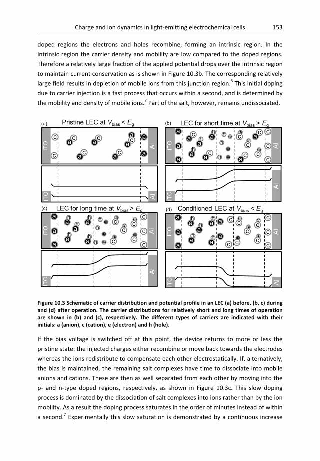
Charge and ion dynamics in light‐emitting electrochemical cells 153
doped regions the electrons and holes recombine, forming an intrinsic region. In the
intrinsic region the carrier density and mobility are low compared to the doped regions.
Therefore a relatively large fraction of the applied potential drops over the intrinsic region
to maintain current conservation as is shown in Figure 10.3b. The corresponding relatively
large field results in depletion of mobile ions from this junction region.8 This initial doping
due to carrier injection is a fast process that occurs within a second, and is determined by
the mobility and density of mobile ions.7 Part of the salt, however, remains undissociated.
Figure 10.3 Schematic of carrier distribution and potential profile in an LEC (a) before, (b, c) during and (d) after operation. The carrier distributions for relatively short and long times of operation are shown in (b) and (c), respectively. The different types of carriers are indicated with their initials: a (anion), c (cation), e (electron) and h (hole).
If the bias voltage is switched off at this point, the device returns to more or less the
pristine state: the injected charges either recombine or move back towards the electrodes
whereas the ions redistribute to compensate each other electrostatically. If, alternatively,
the bias is maintained, the remaining salt complexes have time to dissociate into mobile
anions and cations. These are then as well separated from each other by moving into the
p‐ and n‐type doped regions, respectively, as shown in Figure 10.3c. This slow doping
process is dominated by the dissociation of salt complexes into ions rather than by the ion
mobility. As a result the doping process saturates in the order of minutes instead of within
a second.7 Experimentally this slow saturation is demonstrated by a continuous increase
(a) (b)
(d)(c)
ITO Al
ITO Al
ac a
c
ca
ca
ca
ca
ca
a
Pristine LEC at Vbias < Eg
ITO
Al
ITO Al
c
c
c
a
a
a
ec
ec
ec
ha
ha
ha
h
h
h e
e
e
LEC for short time at Vbias > Eg
ca
ca
ca
ca
ITO Al
ITO Al
ea c
a
a
c
c
c
ec
ec
ec
ec
ha
ha
ha
ha
ha
a
c
c
a
Conditioned LEC at Vbias < Eg
ITO
Al
ITO Al
c
c
c
a
a
a
ec
ec
ec
ec
ec
ha
ha
ha
ha
ha h
h
h e
e
e
LEC for long time at Vbias > Eg

154 Chapter 10 | Large magnetic field effects in electrochemically doped polymer LECs
of current while the efficiency decreases. The efficiency decrease is related to exciton
quenching at doping sites.9 This quenching is an interaction between singlet excitons and
trapped charges. It is typically a strong effect in LECs, as p‐i‐n junction formation allows for
relatively large numbers of carriers close to a narrow recombination zone. As triplet
excitons typically live longer than singlet excitons, interactions between triplet excitons
and trapped charges are likely present as well, although they cannot be directly observed
in the efficiency. Such interactions will, however, prove to be important for the OMAR
effects described later in this chapter.
When removing the bias voltage after such a long transient, again the excess electronic
carriers will recombine or be collected by the electrodes. However, as the doping density
is maximized in this case, a larger amount of doping is expected to remain trapped inside
the device as illustrated in Figure 10.3d. The difference in quasi‐Fermi levels of the p‐ and
n‐type doped regions then leads to a compensating electric field in the junction region. In
planar cells it has been observed that the sign of the electric field in the junction region
changes after removal of the bias voltage.10 This is drawn in Figure 10.3d. During
operation the electrons and holes cause uncompensated space charge in the junction
region. After switch‐off the electrons and holes recombine, leaving anions and cations to
form space charge in this region. The anions and cations in the junction region either
originate from ions that were already trapped in this region or ions that entered the
junction region by drift and/or diffusion. In either case, the removal of the bias voltage
leads to a switch in sign of the polarity of the electric field in the p‐i‐n junction. In this
state the electronic transport is strongly influenced by the Coulomb traps formed by the
ions in the p‐i‐n junction. This is an interesting case for studying OMAR as charge traps are
known to enhance the magnitude of OMAR in general.11
The magnetic field effects reported in this chapter are rationalized in the next sections in
the light of the device physics explained above. In short, conditioning changes the device
operation in the voltage regime at and below the semiconductor bandgap. In a
conditioned device the active layer contains ions that trap electronic charges as well as
uncompensated ions acting as Coulomb traps.
10.4.2 MagneticfieldeffectsThe magnetic field effects observed in Figure 10.1b and Figure 10.2 can be separated by
their respective linewidths: an MC and MEL effect with B0 ≈ 2.2 mT and an MEL effect with
B0 ≈ 220 mT. The low‐field effects arise at magnetic fields that are similar in size as that of
the hyperfine fields, which are mainly caused by the surrounding hydrogen nuclei. In the
absence of an external magnetic field, these hyperfine fields are randomly oriented,
enabling spin mixing of nearby carriers. Sufficiently large external fields on the other hand
reduce spin mixing. In literature, several models have been proposed in which hyperfine

Charge and ion dynamics in light‐emitting electrochemical cells 155
interactions are relevant for electron‐hole interactions4, 12‐13 or electron‐electron and hole‐
hole interactions.14‐15
To first give an overview of all for this case relevant processes regarding electronic charge
transport and recombination, a schematic was drawn in Figure 10.4. The schematic starts
from free electrons and holes. When a free charge comes in the vicinity of another charge
of equal polarity, a polaron pair is formed with either singlet or triplet character. As both
carriers are on different sites, hopping through the semiconductor can lead to spin mixing,
which is induced by the presence of random hyperfine fields. Both charges can, however,
only arrive at the same site if the polaron pair has a singlet spin‐state. In that case a
bipolaron is formed. Polaron pairs and bipolarons also dissociate, leading again to free
electrons or holes.
Free electrons and holes can also meet each other and form electron‐hole pairs with
either singlet or triplet character. This process is favored by Coulomb attraction, which is
rather strong in organic semiconductors due to the relatively low dielectric constant. The
spin‐state of the electron‐hole pairs can again be mixed by hopping through the
semiconductor having random hyperfine fields. In case when the electron and hole arrive
on the same site an exciton is formed with a fixed spin‐state. In case when the exciton
does not interact with any surrounding particles, the exciton will ultimately decay to the
ground state.
In this work only the following interactions involving excitons are considered: triplet‐
triplet annihilation, which is not shown in Figure 10.4, and triplet‐polaron interaction. In
the latter case, the triplet exciton and polaron form a doublet or a quartet spin state. The
doublet and quartet manifold show a zero field splitting and these spin states can be
mixed. Ultimately, either the exciton‐polaron complex dissociates in a triplet exciton and a
polaron, or the complex decays by energy or charge transfer resulting in the loss of the
exciton, whereas the polaron remains. Singlet exciton quenching on polarons is not
considered in this work because of the orders of magnitude shorter singlet lifetime in PPV.
In Figure 10.4 gray arrows are drawn to indicate the magnetic field dependent transitions
between polaron pairs of equal and opposite charges and between a combination of a
triplet exciton and a trapped charge. In the next sections these interactions are discussed
in relation to the experimentally obtained magnetic field effects in conditioned LECs.

156 Chapter 10 | Large magnetic field effects in electrochemically doped polymer LECs
Figure 10.4 Schematic representation of all particles and processes that can lead to magnetic field effects in current and electroluminescence. Note that this is not a strict energy diagram.
10.4.3 Low‐fieldeffectsinefficiencyThe non‐zero Mη shown in Figure 10.2c and d indicates that, by application of a magnetic
field, a change in singlet:triplet ratio has been established. Such a magnetic field effect
originates from magnetic‐field dependent singlet‐triplet interconversion within the
electron‐hole pair prior to exciton formation. To describe this effect we used the two‐site
model that was recently introduced by Kersten et al.4 This model describes the exciton
formation process by considering the final hop of an electron from the site where it
resides to a site where a hole is residing, or vice versa. As electron and hole are on
different sites, the spins of both carriers can change due to hyperfine mixing because the
exchange coupling is relatively small. The rate of spin mixing is proportional to the
hyperfine precession frequency: ωhf = gµBBhfħ‐1, where g is the g‐factor; g ≈ 2 is taken in
this case for both electrons and holes, µB is the Bohr magneton and Bhf is the strength of
the hyperfine field. The exciton formation itself can be described by the hopping rates kT
_
Polaron pairs
hf
Trapped e/h
ZFS
Free e & h
e+h pair
exciton
S
S T
T
DQ
Ground state
Exciton + trapped e/h
Free e/h
S T
+
+_
_ _
_+
_+ +
Bipolaron S
hf
+_
+_

Charge and ion dynamics in light‐emitting electrochemical cells 157
and kS that are slightly different for triplet (T) and singlet (S) exciton formation due to a
difference in energy and wave function. Further details on this model can be found in Ref.
4.
The model is used to determine the parameters needed to obtain similar values of MC and
Mη as in the experiment. The maximal experimental value of MC, ‐0.09, was taken from
Figure 10.2 at Vbias = 1.25 V. The corresponding value for Mη at the same bias voltage
could not be determined, as the electroluminescence was below the detection limit in the
experiment. Therefore a value of Mη = 0.15 is assumed, which can be deduced by
extrapolation to Vbias = 1.25 V.16 The model was used to calculate the Mη for different
ratios i) of the singlet and triplet exciton formation rates, kS/kT, and ii) of the triplet exciton
formation rate and spin mixing rate, kT/ωhf. Mη is plotted in a contour plot in Figure 10.5a.
From the contour plot a set of parameters can be deduced for which Mη ≈ 0.15. This set is
indicated by the white dashed line in Figure 10.5a. As a check whether this set comprises
realistic values of these parameters, we compared the obtained results with parameters
reported earlier in pure MDMO‐PPV: kS/kT = 0.7 and kT/ωhf = 1.1.4 These parameters are
close to the parameters obtained in the modeling here (see white arrow in Figure 10.5a),
proving that the model description for the Mη effect is possible.
Figure 10.5 Contourplots of (a) Mη and (b) MC as a function of kS / kT and kT / ωhf for the two‐site model. The dashed lines in (a) and (b) indicate the contours of the experimentally obtained values of Mη and MC (see Figure 10.2d).
What is left to explain is the diminishing of the low‐field effect in the efficiency at higher
bias voltages as observed in Figure 10.2d: both the negative low‐field MFE in current and
the positive low‐field MFE in electroluminescence decrease, resulting in a lowering of the
low‐field MFE in efficiency. This can be explained by a shift in the contour plot towards

158 Chapter 10 | Large magnetic field effects in electrochemically doped polymer LECs
larger values of kT/ωhf starting at
10log kT/ωhf = 0. In that case, Mη is observed to be
reduced. An increase of the parameter kT/ωhf is likely, as at low bias voltages the carrier
density is low in the LEC, favoring localization of polarons and increasing the contribution
of traps to transport. Especially at sub‐bandgap voltages, ions in the junction region are
expected to act as traps (see Figure 10.3d) as their space charge is dominant in the
junction region. This means that the mobility, which is related to the hopping rate kT, is
relatively low at sub‐bandgap bias voltages. When increasing the bias voltage, the trap
states fill up so that free polarons cannot relax into these states. This as well as the larger
carrier densities leads to an enhanced carrier mobility, hence a larger hopping rate.17‐18 As
the hopping rate of polarons is related to the exciton formation rate; also the latter is
enhanced by the larger bias voltage. Such an enhancement means a shift towards the
right‐hand side in the contour plot shown in Figure 10.5a, which implies a reduction in Mη
as well.
In summary, the two‐site model shows that the observed low‐field effect in Mη at bias
voltages around the bandgap originates from an interplay between i) a magnetic field
dependent spin mixing rate, ii) a singlet exciton formation rate and iii) a triplet exciton
formation rate of an electron‐hole pair. Suppression of spin mixing effectively favors
exciton formation with the lowest rate, i.e. the singlet exciton formation, leading to an
enhanced efficiency. The roll‐off of Mη at higher voltages is arguably due to an enhanced
hopping rate, leading to an enhancement of both the singlet and triplet exciton formation
rate whereas the spin mixing rate remains the same. As a consequence the effects of spin
mixing and the external magnetic field are reduced, leading to smaller values of Mη.
10.4.4 Low‐fieldeffectsincurrentFor the rationalization of the negative MC in conditioned LECs biased below the bandgap,
the following magnetic field dependent interactions were considered (see also Figure
10.4): polaron pair interactions between equal carrier types, polaron pair interactions
between unequal carrier types, the interaction between excitons and trapped charges and
the influence of the triplet exciton density on the dielectric constant.
10.4.4.1 PolaronpairwithequalcarriersTo determine whether magnetic field dependent polaron pair interactions between equal
carrier types in the doped regions play a role in the observed MC, an electrochemical
transistor as described in Figure 8.8 and similar to Ref. 19 was fabricated. In this transistor
either n‐ or p‐type doping is established, excluding any excitonic or recombination effects.
No MC effects were observed at any doping level. Also during and after de‐doping no MC
was observed. This strongly suggests that spin‐related interactions between electrons and
electrons or holes and holes in electrochemically doped and partially de‐doped MDMO‐

Charge and ion dynamics in light‐emitting electrochemical cells 159
PPV do not play a significant role in transport. Moreover, it excludes magnetic field
dependent interactions between electronic and ionic species.
10.4.4.2 PolaronpairwithunequalcarriersAnother option to explain the MC is polaron pair interaction between unequal carrier
types during exciton formation. This interaction can only occur if both electrons and holes
are injected. Despite biasing the LEC with a bias voltage below the bandgap, both types of
carriers can still be injected.20 A sign that this is indeed the case is the L‐V characteristic of
the conditioned device as opposed to the unconditioned device in Figure 10.1a. For 2.1 V
< Vbias < 2.4 V the appearance of electroluminescence is observed in the conditioned
device. For lower bias voltages electroluminescence may still be present but lies below the
detection limit of the diode. To further substantiate this statement the 1D numerical drift‐
diffusion model was used to calculate carrier density, recombination and potential profiles
in an LEC before (Vbias = 1 V), during (Vbias = 4 V) and after (Vbias = 1 V) conditioning. These
profiles are plotted in Figure 10.6a‐c. The trapping by dopants was simulated by first
biasing the device at 4 V, followed by a short relaxation at Vbias = 0 V after which the ions
were artificially immobilized in the model. The short time span at which the device has
been biased at 0 V determines the trapped doping density. The profiles in Figure 10.6a‐c
show that due to the fixed doping (Figure 10.6a) and the formation of Ohmic contacts by
p‐ or n‐type doping (Figure 10.6c), recombination still takes place even though the device
is biased (Vbias = 1 V) below the bandgap (Egap = 2.2 eV). In the case shown here, the
recombination has been lowered by a factor 106 compared to the case of Vbias = 4 V. This
is in line with the luminance being below the detection limit of the experimental setup.
The profiles in Figure 10.6a‐c furthermore show that the vast majority of the injected
carriers form excitons instead of being extracted by the contacts: electron and hole
densities only overlap in the central region of the device. This means that exciton
formation limits the current passing through the cell. This knowledge can be used to
determine the magneto‐conductance by considering the sum of singlet and triplet exciton
formation. Therefore it is possible to determine the magneto‐conductance related to spin
mixing and singlet/triplet exciton formation by using the two‐site model presented in the
previous section. As shown in Figure 10.5a, the absence of spin mixing induced by a
magnetic field enhances the singlet:triplet ratio, as evidenced by a positive Mη.
Reasonable values of Mη were found for ks/kT < 1, see Figure 10.5a. Hence, the total
exciton formation rate decreases with magnetic field. This decrease leads to a reduced
current, as the current is proportional to the exciton formation rate. In Figure 10.5b a
contour plot of the MC is shown. Here, the MC is calculated from the sum of the exciton
formation rates weighted by the calculated singlet:triplet ratio. The black, dashed lines
indicate the parameters at which MC = ‐0.09 is obtained. The gray dashed line is copied
from Figure 10.5a to indicate the parameters at which Mη = 0.15. The mismatch between

160 Chapter 10 | Large magnetic field effects in electrochemically doped polymer LECs
the gray and black lines indicate that no solution exists for which MC = ‐0.09 and Mη =
0.15. The corresponding values of the MC on the gray dashed line lie between 0.00 and ‐
0.03, i.e. 0 % to ‐3 %. This is not in line with the experimentally determined ‐10 % (see
Figure 10.1b). Therefore this mechanism cannot be the main cause of the observed MC
effects.
Figure 10.6 Calculated profiles of (a) electron and hole density, (b) recombination and (c) potential in an unconditioned LEC at Vbias = 1 V (dotted lines), the same LEC at Vbias = 4 V (dashed lines) and at Vbias = 1 V (solid lines) after conditioning. Conditioning is modeled by allowing the device to reach steady‐state at Vbias = 4 V, followed by a short time relaxation to allow part of the doping to deplete. After that the ion mobility was set to zero to artificially trap electronic charges with immobile ions. (d, e) Calculated current density and MC(V) according to the numerical drift‐diffusion model (d) with and (e) without zero ion mobility. In (d), leakage current is included: (Jleakage = 10
‐11∙Vbias).
10.4.4.3 Magnetic field dependent triplet density: effect on triplet exciton‐polaronsinteractions
So far, polaron pair interactions were studied by means of an electrochemical transistor
and the two‐site model. The results of these studies prove that the negative MC in LECs is
not related to polaron pair interactions in the doped regions (electron‐electron, hole‐hole)
or in the junction region (electron‐hole). Therefore, excitonic interactions may need to be
included. To obtain an effect on the current density, the excitons need to interact with
polarons either in the doped regions or in the recombination zone. As excitons are only
formed in the recombination zone, the interaction is most likely to take place in or just
next to this region. Due to the relatively large lifetime of triplet excitons, most likely their
interaction with polarons is dominant.21‐24 The triplet exciton density itself is magnetic
10-6
10-5
10-4
10-3
10-2
10-1
Car
rier
den
sity
(nm
-3)
holes electrons
10-6
10-4
10-2
100
102
Recombination
Re
com
bina
tion
(a.u
.)
0 20 40 60 80 100
-4
-3
-2
-1
0
Pot
entia
l (eV
)
Potential
Position (nm)
10-14
10-12
10-10
10-8
10-6
10-4
Cu
rren
t den
sity
(A
m-1)
-10
-8
-6
-4
-2
0
2
without leakage with leakage
MC
(%
)
0 1 2 3 410-8
10-7
10-6
10-5
10-4
10-3
Cur
rent
den
sity
(A
m-1)
Bias Voltage (V)
-10
-8
-6
-4
-2
0
2
MC
(%
)
(a)
(b)
(c)
(e)
(d)

Charge and ion dynamics in light‐emitting electrochemical cells 161
field dependent, which followed from the change in singlet:triplet ratio as calculated in
Figure 10.5a. Polarons in the intrinsic region are expectedly trapped in deep states
because of their relatively low density for Vbias < Egap (Figure 10.6a) and due to
uncompensated immobile ions that lead to the space charge in the junction region (Figure
10.6c). The interaction relevant here is then recombination of a trapped polaron and a
triplet exciton producing a molecule in the ground state and a polaron, as shown in the
bottom right in Figure 10.4. The recombination process can then lead to detrapping of the
polaron either due to energy or charge transfer from the triplet exciton. Hence the triplet
exciton density, which itself is magnetic field dependent, can effectively change the
mobility of polarons and concurrently the current passing through the cell. Note that this
effect would be absent in a non‐conditioned device, as then no excitons are formed for
Vbias < Egap, and because of the lesser importance of trapping, see paragraph 10.4.1. For
Vbias > Egap the trap states will be filled, resulting in trap‐free carrier transport. This reduces
the effect of detrapping on the total current density. Hence the MC rolls off at higher bias
voltages, which is indeed observed in Figure 10.1b. Note that OMAR experiments on LECs
by Vardeny et al.1 did not show the negative MC as observed here. They found that during
operation electron and hole transport was asymmetric, leading to pinning of the
recombination zone to one of the electrodes. Therefore, bipolar injection can in that work
argued to be absent for Vbias < Egap, as either one of the doped regions has not developed
properly during operation.
A remark is in place regarding a possible magnetic field dependence of triplet‐polaron (T‐
P) interactions (see Figure 10.4). If interactions between triplet excitons and trapped
polarons indeed play a role, a high‐field MFE is expected related to the zero‐field splitting
of the resultant doublet and quartet manifold.25 In anthracene, for example, the rate of
triplet quenching by polarons was found to be magnetic field dependent.26‐27 As MDMO‐
PPV is a singlet emitter, this effect cannot be observed in the electroluminescence. The
reason why no high‐field MFE in the current is observed is unknown to us.
To attempt to explain the absence of a high‐field MFE, the following processes need to be
considered: a triplet exciton can either decay to the ground state or form a triplet polaron
pair if a (trapped) polaron is near. The triplet‐polaron pair either dissociates again in a
triplet exciton and a polaron or the triplet exciton is quenched, leading to a molecule in
the ground state and an energetically excited polaron. The quenching process is likely
dependent on the spin state, which can be altered by spin mixing related to the zero‐field
splitting. In case quenching is not possible due to the spin configuration, the pair has to
dissociate. The resultant polaron then remains trapped, whereas the triplet exciton can
either decay or form a new triplet‐polaron pair. In case the decay rate of triplet excitons is
relatively small, it is most likely that triplet excitons sequentially form pairs with different
trapped polarons until the right spin‐configuration for quenching is obtained. In such a

162 Chapter 10 | Large magnetic field effects in electrochemically doped polymer LECs
case no high‐field MFE in the current is expected. In the conditioned LEC discussed here
the latter seems to be the case. One argument is the fact that singlet exciton quenching is
already highly efficient in the doped regions, whereas the lifetime of singlets is typically a
factor 103 smaller in MDMO‐PPV than the lifetime of triplets. Furthermore, in a recent
paper, Friend et al. characterized both triplet‐triplet annihilation as well as triplet‐charge
quenching as the dominant triplet decay mechanisms in polymer LEDs.28 Therefore it is
most likely that in the conditioned LEC no high‐field MFE is observed. Another possible
explanation for the absence of a high‐field MFE is that the presence of ions favors spin
mixing, suppressing effectively any magnetic field dependence of the transition between
quartet and doublet states.
10.4.4.4 Magneticfielddependenttripletdensity:effectondielectricconstantAn alternative explanation of MC in OLEDs was given in terms of a magnetic field
dependent change in the dielectric constant ε.29 The recombination current is
proportional to ε via the Langevin factor ⁄ . A change of 10 % of ε would
then be necessary to explain the observed MC of ‐10 %. The change in ε can originate
from an altered triplet exciton density. The small dipoles formed by the triplet excitons are
then expected to enhance the dielectric constant. If this would be the case here, then, in a
hypothetical situation, a dramatic change of ε far beyond 10 % would be expected when
comparing an unbiased device and a device biased at e.g. 4 V. The difference in triplet
density would be significantly larger than at V < Eg with and without a magnetic field.
Large changes in the dielectric constant in similar LECs biased at 0 V and 4 V have,
however, not been observed in impedance measurements.7 Hence, we do not think that
this alternative explanation is applicable to our results. On the contrary, we suggest that
the effects observed in the air‐treated MEH‐PPV diodes in Ref. 29 can also be described by
a triplet exciton dependent detrapping of polarons.
10.4.4.5 DevicesimulationsTo check whether the proposed mechanism of triplet exciton assisted detrapping of
polarons can explain the observed bias voltage dependence of the MC (see Figure 10.2d),
numerical drift‐diffusion simulations were performed (see paragraph 10.3 and appendix A
for more details). The model does not explicitly describe spin states or magnetic field
effects. Nonetheless, these effects can be mimicked by altering parameters that are
supposed to be magnetic field dependent.30 In paragraph 10.4.4.3, the MC was attributed
to an effective change in polaron mobility in the junction region. To model the effect of
such a mobility change on the device current, the modeling results of the conditioned LEC
shown in Figure 10.6a‐c (straight lines) were used as starting points. Changing the polaron
mobility in the complete device gives the trivial result of a proportional change in current.
It was argued above, however, that only the mobility in the junction region is affected by
interaction with triplet excitons. The carrier mobility in the junction region affects carrier

Charge and ion dynamics in light‐emitting electrochemical cells 163
transport as well as carrier recombination. Recombination is described by the Langevin
description in the model and is proportional to the sum of the electron and hole
mobilities: , where the Langevin factor is ⁄ . Here, n and p are
the respective electron and hole densities, q is the elementary charge, µn and µp are the
electron and hole mobilities, respectively, and ε is the dielectric constant. To model the
effect of an altered recombination rate due to a reduced carrier mobility, a prefactor Rpre
was introduced in the Langevin formula for the recombination rate: . A
prefactor of 0.9 was used, mimicking a reduction of 10 % of the carrier mobility in the
junction region. The magneto‐conductance was then determined by comparing the
current for simulations with Rpre = 0.9 and 1.0. Similar modeling results were obtained
when instead of changing Rpre, the electronic charge carrier mobility in the recombination
zone was altered by 10 %.31
In Figure 10.6d and e modeled J‐V and MC‐V characteristics are shown in, respectively, a
conditioned and a pristine device operating in steady‐state at different bias levels. In the
conditioned device the ions are artificially frozen at their positions after conditioning by
setting the ion mobility to zero; in the pristine device the ion mobility is nonzero, as this
corresponds to a non‐conditioned device. In the pristine device no MFE in current is
observed, whereas in the conditioned device the decrease of the carrier mobility with
magnetic field has resulted in a MFE in the current, denoted as MC = (IRpre=0.9‐IRpre=1)/IRpre=1
for Vbias < Egap. Here IRpe=0.9 and IRpre=1 represent the current for the cases when Rpre = 0.9 or
1.0. To make the modeling results resemble the experimental results at bias voltages
around 0 V (e.g. Figure 10.1b), a small, linear leakage current was added to the simulated
current density. The leakage current dominates the total current at these relatively small
bias voltages, leading to an effective reduction of MC. The small MC values around Vbias = 0
V may furthermore also be related to the relatively low generation rate of triplet excitons
due to the low current density here.
For Vbias > Egap a positive MC is observed in Figure 10.6d due to two artificial problems in
the modeling. First of all, in reality the high bias voltage would enable the ions to move.
The results in Figure 10.6e show what the effect of mobile ions on the MC would be: MC ≈
0. Secondly, polaron detrapping in the junction region becomes less dominant: trap states
are completely filled resulting in polarons to be in energetically higher‐lying states, leading
to a higher mobility. The current is therefore not dominated by traps anymore. As a result,
the T‐P effect is not likely to enhance the carrier mobility in this bias range: a change of 10
% in electronic carrier mobility is most likely an overestimate. Therefore, the part of the
modeling for Vbias > Egap can be ignored.
The modeling results can be summarized as follows: a reduction of the carrier mobility in
the recombination region can only reduce the total current through the device in the

164 Chapter 10 | Large magnetic field effects in electrochemically doped polymer LECs
specific case that a fixed p‐i‐n junction structure is present. This was achieved in the model
by reducing the ion mobility to 0 during steady‐state operation at Vbias = 4 V. For this, the
applied bias voltage must be below the bandgap of the semiconductor. In case Vbias > Egap
the effect of the frozen p‐i‐n junction is reduced due to the formation of electronic space
charge. Experimentally, the negative MC is measured at the same conditions as described
here: A fixed p‐i‐n junction is present and electronic space charge is absent due to first
conditioning the device at Vbias = 4 V followed by operation at Vbias < Egap.
Considering all results together we attribute the negative MC in conditioned LECs to
polaron‐triplet exciton interactions that lead to an enhanced carrier mobility in the trap‐
dominated intrinsic region. This effect is unique in LECs as opposed to OLEDs. In OLEDs,
transport occurs by percolation through optimal pathways, which typically are not
dominated by traps. In conditioned LECs biased at low bias voltages, the trap density is
large relative to the carrier density so that transport occurs from trap to trap. Interaction
with triplet excitons can help to release carriers from these traps by transfer of energy
from the triplet exciton to the trapped polaron. The observed magnetic field dependence
itself does not originate from T‐P interactions, but from the change in triplet exciton
density. The triplet exciton density changes due to a change in singlet:triplet exciton
formation ratio discussed in the previous section.
10.4.5 High‐fieldMFEinefficiencyThe last observed MFE that has not been discussed yet is the effect in the efficiency that
arises at B0 = 220 mT and Vbias > Egap as shown in Figure 10.2d. The relatively large size of
the characteristic magnetic field B0 indicates a mechanism related to zero‐field splitting.
Furthermore, the effect only changes the electroluminescence, whereas it has no effect on
the current. Species that may be involved because of their presence in the recombination
zone are polarons and singlet and triplet excitons. Singlet excitons can interact with
polarons leading to quenching. This quenching is, however, not magnetic field dependent.
A possible MFE in the electroluminescence can originate from delayed fluorescence (DF)
arising from triplet‐triplet annihilation (TTA).25, 32‐33
A pair of triplets can produce nine possible spin states with equal probability: a quintet, a
triplet and a singlet state. Due to spin conservation, only the latter can annihilate forming
an excited and a ground‐state singlet state. The excited singlet state can then relax by
emitting a photon. This process is called delayed fluorescence (DF) and was recently
shown to be of importance in OLEDs.34 Mixing between all nine spin states is possible
when the Zeeman splitting is equal to or smaller than the zero‐field splitting. If on the
other hand a relatively large magnetic field is applied, then the Zeeman splitting
suppresses spin mixing, leading to a reduced fluorescence. The high‐field effect shown in
Figure 10.2d is negative, which is in line with the previous discussion. The zero‐field
Charge and ion dynamics in light‐emitting electrochemical cells 165
splitting parameter of MDMO‐PPV is D ≈ 60 mT,35‐36 which corresponds with the
experimental results presented in Figure 10.2b and d: the high‐field effect appears roughly
at 50 mT. The observed voltage dependence can be explained by the enhancement of the
current, leading to a larger triplet exciton density. Accordingly, the probability of triplet‐
triplet encounters grows, leading to an enhanced contribution of DF from TTA to
fluorescence. Additionally, it is likely that the triplet‐triplet interactions are in competition
with the triplet‐polaron encounters, which were argued in the previous section to result in
a negative MC. The enhanced probability for TTA at larger bias voltages may therefore
result in an effective reduction of triplet‐polaron encounters leading to a reduced MC
effect as is experimentally observed in Figure 10.2d (for Vbias > 1.2V). These results indicate
that part of the luminance in LECs is comes from DF by TTA. The maximal contribution of
this process to the total electroluminescence can be determined under the following
assumptions: i) all triplets form pairs; ii) the singlet:triplet ratio is close to 25:75 and iii) the
magnetic field is large enough to prevent any spin mixing. In that case a fraction of 1/18 of
the triplets is converted in singlets, resulting in roughly 14 %37 of the total fluorescence
originating from DF. Removal of the magnetic field then enhances this contribution at Vbias
= 4 V to 17 %. This means that a significant fraction of the electroluminescence in PPV‐
based LECs originates from DF by TTA.
10.5 ConclusionsIn summary, we have shown that light‐emitting electrochemical cells can show large
magnetic field effects because of trap‐dominated transport and recombination in a
relatively narrow region due to electrochemical doping. Large negative magneto‐
conductance values of around ‐12 % are observed in conditioned LECs simultaneously with
a positive magneto‐efficiency. Both effects originate from the competition between
magnetic field dependent spin mixing and the formation rates of singlet and triplet
excitons. The change in singlet:triplet ratio leads to the enhanced efficiency. The reduced
triplet exciton density is suggested to lead to a reduction in polaron detrapping in the
recombination zone, resulting in a reduced current density. At bias voltages that
significantly exceed the semiconductor bandgap, a negative magneto‐electroluminescence
effect is observed arising at relatively large magnetic fields of 220 mT. This effect is
attributed to delayed fluorescence which originates from magnetic field dependent
triplet‐triplet annihilation. The contribution of delayed fluorescence to the total light
output of the LEC is estimated to be at most 17 %.

166 Chapter 10 | Large magnetic field effects in electrochemically doped polymer LECs
References
[1] G. Ni, T. D. Nguyen, Z. V. Vardeny, Appl. Phys. Lett. 98 (2011) 263302.
[2] T. D. Nguyen, G. Hukic‐Markosian, F. J. Wang, L. Wojcik, X. G. Li, E. Ehrenfreund, Z. V. Vardeny, Nat.
Mater. 9 (2010) 345.
[3] Ö. Mermer, G. Veeraraghavan, T. L. Francis, Y. Sheng, D. T. Nguyen, M. Wohlgenannt, A. Köhler, M. K.
Al‐Suti, M. S. Khan, Phys. Rev. B 72 (2005) 205202.
[4] S. P. Kersten, A. J. Schellekens, B. Koopmans, P. A. Bobbert, Phys. Rev. Lett. 106 (2011) 197402.
[5] W. Wagemans, W. J. Engelen, F. L. Bloom, B. Koopmans, Synth. Met. 160 (2010) 266.
[6] U. Niedermeier, M. Vieth, R. Patzold, W. Sarfert, H. von Seggern, Appl. Phys. Lett. 92 (2008) 193309.
[7] S. van Reenen, R. A. J. Janssen, M. Kemerink, Adv. Funct. Mater. 22 (2012) 4547.
[8] S. van Reenen, P. Matyba, A. Dzwilewski, R. A. J. Janssen, L. Edman, M. Kemerink, J. Am. Chem. Soc.
132 (2010) 13776.
[9] S. van Reenen, T. Akatsuka, D. Tordera, M. Kemerink, H. J. Bolink, J. Am. Chem. Soc. 135 (2013) 886.
[10] P. Matyba, K. Maturova, M. Kemerink, N. D. Robinson, L. Edman, Nat. Mater. 8 (2009) 672.
[11] J. Rybicki, R. Lin, F. Wang, M. Wohlgenannt, C. He, T. Sanders, Y. Suzuki, Phys. Rev. Lett. 109 (2012)
076603.
[12] V. N. Prigodin, J. D. Bergeson, D. M. Lincoln, A. J. Epstein, Synth. Met. 156 (2006) 757.
[13] P. Desai, P. Shakya, T. Kreouzis, W. P. Gillin, Phys. Rev. B 76 (2007) 235202.
[14] P. A. Bobbert, T. D. Nguyen, F. W. A. van Oost, B. Koopmans, M. Wohlgenannt, Phys. Rev. Lett. 99
(2007) 216801.
[15] S. P. Kersten, S. C. J. Meskers, P. A. Bobbert, Phys. Rev. B 86 (2012) 045210.
[16] 0.15 is obtained by taking the measured value of the LFE MC at 1.25 V (= ‐0.09) and by extrapolating
the LFE MEL to 1.25 V (~ +0.06). The corresponding value of Mη results from 0.06 ‐ 0.09 = 0.15. [17] H. Shimotani, G. Diguet, Y. Iwasa, Appl. Phys. Lett. 86 (2005) 022104.
[18] S. van Reenen, R. A. J. Janssen, M. Kemerink, Org. Electron. 12 (2011) 1746.
[19] M. J. Panzer, C. D. Frisbie, J. Am. Chem. Soc. 129 (2007) 6599.
[20] P. Santhanam, D. J. Gray, R. J. Ram, Phys. Rev. Lett. 108 (2012) 097403.
[21] B. Koopmans, W. Wagemans, F. L. Bloom, P. A. Bobbert, M. Kemerink, M. Wohlgenannt, Philos. Trans.
R. Soc. London, Ser. A 369 (2011) 3602.
[22] J. Yu, R. Lammi, A. J. Gesquiere, P. F. Barbara, J. Phys. Chem. B 109 (2005) 10025.
[23] M. Wittmer, I. Zschokkegranacher, J. Chem. Phys. 63 (1975) 4187.
[24] S. Reineke, K. Walzer, K. Leo, Phys. Rev. B 75 (2007) 125328.
[25] A. J. Schellekens, W. Wagemans, S. P. Kersten, P. A. Bobbert, B. Koopmans, Phys. Rev. B 84 (2011)
075204.
[26] V. Ern, Merrifie.Re, Phys. Rev. Lett. 21 (1968) 609.
[27] V. Ern, Bouchrih.H, J. Fourny, G. Delacote, Solid State Commun. 9 (1971) 1201.
[28] B. H. Wallikewitz, D. Kabra, S. Gelinas, R. H. Friend, Phys. Rev. B 85 (2012) 15.
[29] K. Kanemoto, H. Matsuoka, Y. Ueda, K. Takemoto, K. Kimura, H. Hashimoto, Phys. Rev. B 86 (2012)
125201.
[30] M. Cox, P. Janssen, S. H. W. Wouters, E. H. M. van der Heijden, M. Kemerink, B. Koopmans, Synth.
Met. 173 (2013) 6.
[31] S. van Reenen, S. P. Kersten, S. H. W. Wouters, M. Cox, P. Janssen, B. Koopmans, P. A. Bobbert, M.
Kemerink, Phys. Rev. B 88 (2013) 125203.
[32] Y. Zhang, R. Liu, Y. L. Lei, Z. H. Xiong, Appl. Phys. Lett. 94 (2009) 083307.

Charge and ion dynamics in light‐emitting electrochemical cells 167
[33] R. C. Johnson, Merrifie.Re, P. Avakian, R. B. Flippen, Phys. Rev. Lett. 19 (1967) 285.
[34] Y. F. Zhang, S. R. Forrest, Phys. Rev. Lett. 108 (2012) 267404.
[35] L. S. Swanson, P. A. Lane, J. Shinar, K. Yoshino, F. Wudl, Synth. Met. 50 (1992) 473.
[36] L. S. Swanson, J. Shinar, P. A. Lane, B. C. Hess, F. Wudl, Synth. Met. 50 (1992) 481.
[37] 1 of 9 possible spin states formed by two triplet excitons can generate one singlet exciton: 1/2 x 1/9 =
1/18. A singlet:triplet ratio of 25:75 then means that 75x1/18 ≈ 4 % of delayed singlet excitons are formed. This means that 4/(25+4) ≈ 14 % of the singlet exciton density is due to DF from TTA in case a magnetic field is present. In the absence of a magnetic field spin mixing takes place between the spin states formed by two triplet excitons. The high magnetic field effect improves the efficiency by 3 % at Vbias = 4 V (see Figure 10.2d). As a result the percentage of delayed singlet excitons increases from 4 % to [(25+4)x1.03]‐25 ≈ 5 %. This means that 5/(25+5) ≈ 17 % of the singlet exciton density is due to DF from TTA in case no magnetic field is present.

168 Chapter 10 | Large magnetic field effects in electrochemically doped polymer LECs

*Part of the work presented in this chapter has been published: S. van Reenen, S. Kouijzer, R. A. J. Janssen, M. M. Wienk, M. Kemerink, accepted for publication in Adv. Mater. Interfaces (2014).
Chapter11 Originofworkfunction
modificationbyelectrolytes
An alternative use of electrolytes besides in the active layer of LECs is as thin injection
layers in organic electronics. The microscopic origin behind work function modification by
such polyelectrolytes and tertiary aliphatic amines used as interlayers is however unclear.
Scanning Kelvin probe microscopy is used to determine the work function modification by
thin layers of such materials on different substrates. Both reductions and increases in work
function were found to follow a general mechanism. Such modifications are found to only
take place when the work function modification layer (WML) is deposited on conductors or
semiconductors. On insulators no effect is observed. Additionally, the work function
modification is independent of the WML thickness or the substrate work function in the
range of 3 to 5 eV. This data supports work function modification by dipole formation at
the electrode interface, induced by interaction with its image dipole. Differences in size and
side groups of the ionic constituents lead to differences in approach distance towards the
surface. These differences determine magnitude and direction of the resulting dipole. This
understanding facilitates design and synthesis of new air‐stable and solution‐processable
WMLs for organic electronics.

170 Chapter 11 | Origin of work function modification by electrolytes
11.1 IntroductionThe remarkable efficiency leap from less than 5% to over 10% in the past 7 years makes it
plausible that organic solar cells can evolve into a successful thin film photovoltaic
technology. To this end, further improvements in the sunlight‐to‐electricity conversion
efficiency are still needed. To do so, not only the optoelectronic, active layer should be
considered, but also the connection between this layer and the electrodes. This
connection is facilitated by so‐called work function modification layers (WMLs) that serve
to align the transport levels in the organic semiconductor and the conductor by
modification of the work function. Materials that are often used are poly(3,4‐
ethylenedioxythiophene) poly(styrenesulfonate) (PEDOT:PSS) for improving hole
collection and injection in combination with an indium tin oxide (ITO) electrode and LiF for
the electron contact in combination with an Al metal electrode. A new generation of
WMLs first introduced by Cao et al. is based on polyelectrolytes or tertiary aliphatic
amines, such as poly[(9,9‐bis(3'‐(N,N‐dimethylamino)propyl)‐2,7‐fluorene)‐alt‐2,7‐(9,9‐
dioctylfluorene)] (PFN) and the corresponding ethyl ammonium bromide.1 Although these
materials improve carrier injection or extraction in different organic diode devices,1‐7 the
mechanism behind this improvement is not completely clear. This ambiguity hinders
synthesis, selection and optimization of new WMLs.
Mechanisms that are generally considered to result in electric fields and concomitant
work function shifts at metal‐organic interfaces are doping, charge transfer, and dipole
formation.8‐10 Regarding the work function modification of amine side‐groups, Lindell et
al.11 found by photoelectron spectroscopy and density functional calculations that the
electron donor para‐phenylenediamine chemisorbs onto atomically clean Ni in vacuum.12
Due to partial electron transfer from the amine unit, a work function reduction of 1.55 eV
is achieved, resulting in a less deep Fermi level. This explanation is not likely to hold for
the technologically more relevant procedure on which we shall focus, being the deposition
of WMLs from solution on a metal at atmospheric pressure: the metal is not atomically
clean, which likely inhibits chemisorption. In other work by Zhou et al.13 it is shown that
the work function reduction, at atmospheric pressure, by the amine groups in
poly(ethylenimine ethoxylated) (PEIE), is generally the same on different conductors. They
attributed the effect both to i) orientation of the internal molecular dipole, induced by the
lone pair of the nitrogen atom, and ii) an interfacial dipole due to partial charge transfer
from the amine group after the physisorption on the conductor. Important for
determining the origin of the effect is also the thickness dependence of the amine‐
containing layer.13‐17 In this respect different observations have been made. Xia et al.15
reported an optimum of the work function modification at 8 nm thickness and above,
while Zhou et al.13 and Zhang et al.16 did not observe any thickness dependence. Kim et

Charge and ion dynamics in light‐emitting electrochemical cells 171
al.17 reported a thickness dependence where thicker films resulted in a reduced work
function modification.
Next to PFN, also cationic polyelectrolytes can be used to lower the work function of the
electrode.1, 5‐6 A recent study on conjugated polymer zwitterions revealed a similar
lowering in work function, attributed to electrostatic realignment of the dipolar
zwitterionic side‐chains near the metal interface.18 The formation of interfacial dipoles
and electric field‐induced reorientation of molecules has also been reported.19 Other work
has shown that in the specific case that cationic polyelectrolytes are brought into contact
with fullerenes, doping of fullerenes is observed. 20 This however does not explain the
work function modification of conductors in absence of fullerenes.6
The anionic polyelectrolyte Nafion, which is also an acid, is found to give the opposite
effect compared to cationic polyelectrolytes. A thin film of Nafion on ITO is found to
increase the work function by 0.5 eV,21‐23 which indicates that Nafion can modify the metal
work function. Another anionic polyelectrolyte is poly(4‐styrenesulfonic acid) (H‐PSS), a
component of PEDOT:PSS formulations. In literature evidence exists that a thin layer of H‐
PSS forms on top of PEDOT:PSS.24 Processing of PEDOT:PSS from aqueous dispersions with
different amounts of added sorbitol was found to lead to a reduction in the work function,
which has been interpreted as being the result of removal of the H‐PSS top layer.25
In this chapter we present results which indicate that work function modification by
anionic or cationic (poly)electrolytes and by tertiary aliphatic amines originates from a
single mechanism: the formation of a dipole at the interface. This dipole formation is
driven by the energetic stabilization by its image charges in the contacting
(semi)conductor. On metals coated with a 10 nm thin insulator no dipole orientation or
formation is observed when an additional WML is applied: the work function is not
modified. Equal work function modification is observed by scanning Kelvin probe
microscopy for different thicknesses of PFN or H‐PSS deposited on conductors with
different work functions, ranging from Au to Ca. This excludes charge transfer or doping as
a possible origin of the work function modification. The net direction of the dipole is
furthermore determined by the ability of the positive and negative part of the dipole to
get in the proximity of the (semi‐)conductor. The ability to do so is found to depend on the
geometric properties of the positive and negative part. This behavior is confirmed by
series of tetrabutylammonium halides and H‐PSS, Li‐PSS, and Na‐PSS. The magnitude of
the net dipole can be related to both the ability to orient as well as the density of dipoles
at the interface.

172 Chapter 11 | Origin of work function modification by electrolytes
11.2 MaterialsandmethodsDevice preparation: Devices that were measured consisted of a substrate covered with an
electrode as shown schematically in Figure 11.1.
Figure 11.1 Schematic of the general device layout. SKPM measurements were performed on (a) metal electrodes with and without a work function modification layer (WML) on top and on (b)
metal electrodes covered with a 10 nm layer of conductor/semiconductor/insulator with and without a work function modification layer on top.
The conductor was either sputtered, e.g. indium tin oxide (ITO), vacuum evaporated (Au,
Ag, Al, Ca) or spin coated (poly(3,4‐ethylenedioxythiophene)‐poly(styrenesulfonate)
(PEDOT:PSS, Clevios P VP AI 4083) from Heraeus). Deposition of V2O5 was performed
similarly as described in Ref. 26. Approximately 10 nm thick organic semiconductor or
insulator films were deposited on top by spin coating from solution: [6,6]‐phenyl C70‐
phenylbutyric acid methyl ester (PC70BM, Solenne BV), poly(3‐hexylthiophene) (P3HT,
Aldrich, Mn = 54000‐75000 g mol‐1) and a blend of PC70BM and poly[2,6‐(4,4‐bis‐(2‐
ethylhexyl)‐4H‐cyclopenta[2,1‐b;3,4‐b0]‐dithiophene)‐alt‐4,7‐(2,1,3‐benzothiadiazole)]
(PCPDTBT, Mw = 27700 g mol‐1) from o‐DCB, poly[(9,9‐dioctylfluorenyl‐2,7‐diyl) (PFO), and
a poly(p‐phenylene vinylene) copolymer (Super Yellow PPV, Merck, catalogue number
PDY‐132) from toluene, polystyrene (PS, Aldrich, Mw = 35000 g mol‐1), and
poly(methylmethacrylate) (PMMA, Aldrich, Mw = 105 g mol‐1) from toluene. On top of
these conductors, organic semiconductors and insulators, a 10 nm thick film of poly[(9,9‐
bis(3’‐(N,N‐dimethylamino)propyl)‐2,7‐fluorene)‐alt‐2,7‐(9,9‐dioctylfluorene)] (PFN) was
deposited from either 2 mg ml‐1 methanol (MeOH) + acetic acid (AcOH) (200:1 volume
ratio) or 2 mg ml‐1 toluene. Synthesis of PFN is described elsewhere.[1] Alternatively,
poly(4‐styrenesulfonic acid) (H‐PSS, Aldrich, Mw = 75000 g mol‐1), poly(lithium 4‐
styrenesulfonate) (Li‐PSS, Aldrich, Mw = 75000 g mol‐1) and poly(sodium 4‐
styrenesulfonate) (Na‐PSS, Aldrich, Mw = 70000 g mol‐1) dissolved in ultrapure water (4 mg
ml‐1); tetrabutylammonium (TBA, Aldrich) tetramethylammonium (TMA, Aldrich), and
tetrahexylammonium (THA, Aldrich) salts dissolved in tetrahydrofuran (4 mg ml‐1), or
Nafion (Aldrich, perfluorinated ion exchange resin 5 wt% in mixture of lower aliphatic and
H2O, including 45% water) diluted in ethanol with a 1:200 volume ratio were deposited on
Glass
Electrode(Conductor/Semiconductor/Insulator)
WML
Glass
ElectrodeWML
(a) (b)

Charge and ion dynamics in light‐emitting electrochemical cells 173
top of the mentioned conductors, organic semiconductors, and insulators. Structural
formulae of the above‐mentioned materials are shown in Figure 11.2. The thickness of the
layers ranged between 5 and 10 nm. The thicknesses of the different layers were
measured by a Veeco Dektak profilometer. Device preparation was performed in a N2
filled glovebox in case air‐sensitive materials like Ca, Al or Ag were used.
Figure 11.2 Structural formulae of the organic compounds.
Device characterization: SKPM images were recorded in a glove box under N2 atmosphere
([O2] < 1 ppm and [H2O] < 1 ppm) with a Veeco Instruments MultiMode AFM with
Superyellow PPV
PC70BM PCPDTBT
P3HT
PFO
PMMA
PFN PSS‐R Nafion
THA‐Br TBA‐X TMA‐I
(a) (b) (c)
(d) (e)
(l)
(f) (g) (h)
(i) (j) (k) (m)
PS

174 Chapter 11 | Origin of work function modification by electrolytes
Nanoscope IV controller, operating in lift mode with a lift height of 50 nm. Au‐coated
silicon tips from MikroMasch were employed. During surface potential measurements the
sample was grounded. An Au substrate was used as reference to monitor any tip wear
after multiple measurements. The measurements were carried out at room temperature.
As SKPM is based on nullification of the electric field between tip and sample, no driving
force for ion displacement during characterization exists. The discussed ion work function
shifts and ion displacements therefore have taken place upon or immediately after layer
deposition and not during SKPM probing.
11.3 ResultsanddiscussionTo study the mechanism behind the work function modification by several types of WMLs,
samples as depicted in Figure 11.1 were used. The parameter of interest is the work
function of a conducting, semiconducting, or insulating layer with and without coverage of
the WML. Insulators and intrinsic organic semiconductors, however, do not have a well‐
defined work function as the Fermi level resides in the bandgap. Therefore thin insulating
or semiconducting layers were deposited on top of a metal electrode as illustrated in
Figure 11.1b. The electrostatic potential at the surface is measured by scanning Kelvin
probe microscopy (SKPM) with respect to an Au‐coated tip. The structural formulae of the
materials used as WML or semiconducting/insulating substrate are shown in Figure 11.2.
11.3.1 WorkfunctionreductionbyPFNThe effect of the WML PFN on substrates of conducting (also highly doped semiconductors
like p‐type Si, p‐type doped PEDOT:PSS and n‐type doped V2O5,27 prepared following the
procedure reported in Ref. 26), semiconducting (intrinsic), or insulating nature was
measured as shown in Figure 11.3 and Table 11.1. The qualitative criterium for the
classification of these substrate materials is based on the ability to provide charges which
is proportional to the dielectric response of the substrate material to the WML.
Conductors have a significant amount of mobile charges, which is why we share highly
doped semiconductors in this paper under the same denominator. Intrinsic
semiconductors only provide few charges which are relatively mobile. Insulators do not
contain mobile charges. In Figure 11.3, the horizontal axis represents the work function of
each sample without coverage of the WML: the work function of the substrate. The
vertical axis represents the work function shift of the sample after coverage with the
WML. A negative work function modification corresponds to a reduction of the work
function, i.e. improved electron injection from the substrate.

Charge and ion dynamics in light‐emitting electrochemical cells 175
Table 11.1 Work function modification by PFN.
Work function (eV) Pristine With PFN
ITO 4.4 3.65
Au 4.6 4.0
Ag 4.3 4.0
Al 3.07 2.76
V2O5 5.0 4.2
PEDOT 4.92 4.48
p‐type Si 4.22 3.5
Ca 2.85 1.85
ITO‐PC70BM:PCPDTBT 4.5 4.04
ITO‐PPV 4.55 4.21
ITO‐P3HT 4.24 4.24
Au‐PFO 4.42 4.03
Au‐PC70BM 4.62 4.02
Au‐PS 4.44 4.35
Au‐PMMA 4.59 4.49
Figure 11.3 Work function as measured by SKPM for substrates covered by 10 nm PFN. Substrates are categorized in clean conductors (black circles) and metals coated with a 5 – 10 nm thick film of semiconductor (blue squares) or insulator (red triangles). The symbol filling indicates the specific substrate material as shown in the legend. The horizontal lines indicate the average change in work function for each substrate category. The data is also presented in Table 11.1.
In case PFN was used as WML the work function of the substrate is either reduced or
constant as shown in Figure 11.3. In case the substrate is a conductor (black dots), an
average work function reduction of 0.7 eV (gray line) is obtained. This value is
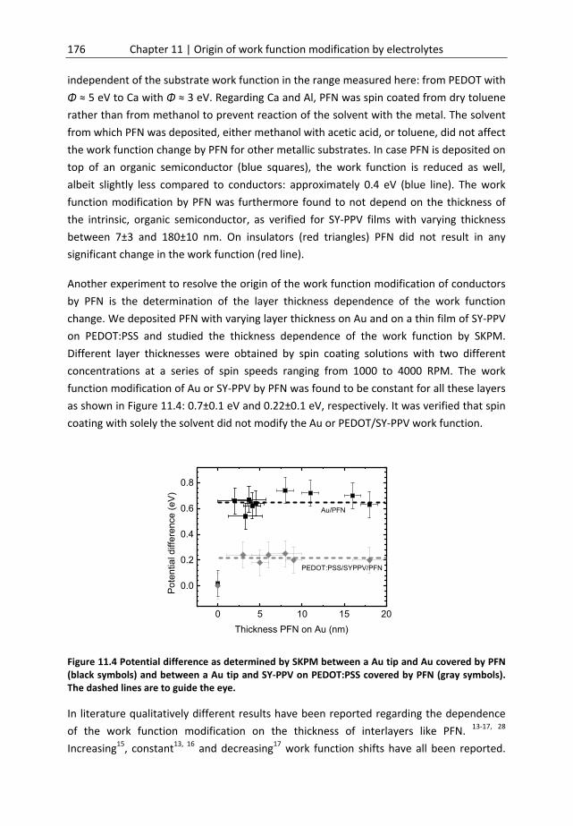
176 Chapter 11 | Origin of work function modification by electrolytes
independent of the substrate work function in the range measured here: from PEDOT with
Φ ≈ 5 eV to Ca with Φ ≈ 3 eV. Regarding Ca and Al, PFN was spin coated from dry toluene
rather than from methanol to prevent reaction of the solvent with the metal. The solvent
from which PFN was deposited, either methanol with acetic acid, or toluene, did not affect
the work function change by PFN for other metallic substrates. In case PFN is deposited on
top of an organic semiconductor (blue squares), the work function is reduced as well,
albeit slightly less compared to conductors: approximately 0.4 eV (blue line). The work
function modification by PFN was furthermore found to not depend on the thickness of
the intrinsic, organic semiconductor, as verified for SY‐PPV films with varying thickness
between 7±3 and 180±10 nm. On insulators (red triangles) PFN did not result in any
significant change in the work function (red line).
Another experiment to resolve the origin of the work function modification of conductors
by PFN is the determination of the layer thickness dependence of the work function
change. We deposited PFN with varying layer thickness on Au and on a thin film of SY‐PPV
on PEDOT:PSS and studied the thickness dependence of the work function by SKPM.
Different layer thicknesses were obtained by spin coating solutions with two different
concentrations at a series of spin speeds ranging from 1000 to 4000 RPM. The work
function modification of Au or SY‐PPV by PFN was found to be constant for all these layers
as shown in Figure 11.4: 0.7±0.1 eV and 0.22±0.1 eV, respectively. It was verified that spin
coating with solely the solvent did not modify the Au or PEDOT/SY‐PPV work function.
Figure 11.4 Potential difference as determined by SKPM between a Au tip and Au covered by PFN (black symbols) and between a Au tip and SY‐PPV on PEDOT:PSS covered by PFN (gray symbols). The dashed lines are to guide the eye.
In literature qualitatively different results have been reported regarding the dependence
of the work function modification on the thickness of interlayers like PFN. 13‐17, 28
Increasing15, constant13, 16 and decreasing17 work function shifts have all been reported.
0 5 10 15 20
0.0
0.2
0.4
0.6
0.8
Au/PFN
Pot
entia
l diff
eren
ce (
eV)
Thickness PFN on Au (nm)
PEDOT:PSS/SYPPV/PFN

Charge and ion dynamics in light‐emitting electrochemical cells 177
Part of these works comprises the characterization of complete devices, which
complicates the interpretation as charge transport is involved as well.14, 16‐17 Use of thicker
layers of insulating materials will reduce the performance due to additional series
resistance. Characterization of the open‐circuit voltage circumvents this issue, although
also the open‐circuit voltage depends on many factors. Characterization of WMLs by
inherently current‐less techniques like SKPM13, 15, 28 excludes these problems, but still one
must ensure that the substrate is completely covered. Incomplete coverage will result in
intermediate results.
11.3.2 ConsideredmechanismsTo determine the nature of the work function reduction by PFN several models proposed
in literature were considered first.13, 15, 20 For each model we inspected its ability to explain
the experimental findings reported here and in literature: the work function modification
is i) dependent on the nature of the substrate: metallic, (organic) semiconducting or
insulating; ii) independent on the work function of the substrate in the range 3.0 – 5.0 eV;
iii) independent of the PFN layer thickness; iv) possible in absence of any semiconductor
which can be electrochemically doped.13
Four models that can describe the work function reduction by the WML PFN are
schematically shown in Figure 11.5: formation of an electric double layer (EDL) after
doping of the WML (Figure 11.5a), charge transfer to or from the conductor (Figure
11.5b), spontaneous dipole orientation in the WML (Figure 11.5c) and the spontaneous
dipole orientation at the interface (Figure 11.5d). A detailed discussion follows in the next
paragraphs about these mechanisms and their ability to describe the observations from
Figure 11.3 and Figure 11.4. Each of these mechanisms is found to have difficulties in
explaining the complete series of findings described above. Therefore an alternative
model is presented later on.
The first model (Figure 11.5a) describes electric double layer formation between a
conductor and a doped material. In organics, doping can be achieved electrochemically by
ions stabilizing electronic charges. Such behavior is e.g. the basis of light‐emitting
electrochemical cells.29‐31 In the polyelectrolytes studied here, mobile ions are present
that can be used for electrochemical doping. Electrochemical doping is, however, not
evident in the semiconductor PFN. Oxidation of tertiary aliphatic amines has nonetheless
been reported and leads to the formation of a cationic compound.32 Such cationic
compounds can stabilize electrons on nearby semiconductors, i.e. electrochemical doping.
The EDL that is formed in case doping is indeed present or takes place would result in a
bias‐dependent depletion of carriers in the doped semiconductor at the interface. The
depletion width would range between 6 and 2 nm for (very high) doping densities of 1025
– 1026 m‐3, respectively, in case a change in built‐in potential of 1 V is assumed. In our

178 Chapter 11 | Origin of work function modification by electrolytes
measurements no thickness dependence of work function modification by PFN is
observed, which indicates that such a depletion layer is absent. Also the fact that PEIE,13
an insulating tertiary aliphatic amine, can change the work function without any form of
doping indicates that the work function change studied in this chapter is not due to doping
and the resulting EDL formation. This however does not exclude that doping takes place in
devices that contain polyelectrolytes.20 The relatively low ionic mobility can result in slow
transient behavior during device operation.5
Figure 11.5 Schematics of possible mechanisms to explain the work function (WF) modification by WMLs: (a) electric double layer formation, (b) charge transfer, (c) spontaneous dipole orientation in the bulk and (d) spontaneous dipole orientation at the interface. The corresponding vacuum levels are shown on top to indicate the spatial potential drop. A legend is shown below.
Modification of the work function can also occur due to dipole formation induced by
integer or partial charge transfer between the substrate and the WML (Figure 11.5b).
Charge transfer can take place in a large variety of circumstances as reviewed by Braun et
al. in Ref. 8. These can be divided in two classes: charge transfer after physisorption or
chemisorption. The latter can occur in case the metal surface of the substrate is atomically
clean, i.e. at pressures as low as 10‐9 mbar. In contrast, the deposition of PFN reported
here took place at atmospheric pressure. Nevertheless, in case a clean substrate surface is
Electric double layer Charge Transfer
Spontaneousdipole orientation
+
+
+
++
+
++
+
++
‐
ΔWF ΔWF
ΔWF
Evac Evac
Evac
+Molecule Oxidized molecule Electron Dipole
(a) (b)
(c)
Metal WML
Spontaneous interfacialdipole orientation
+
‐
ΔWF
Evac
(d)

Charge and ion dynamics in light‐emitting electrochemical cells 179
considered, specific interaction between the WML and the substrate can take place.
Specific interactions are, however, not likely to explain the work function modification by
PFN on conductors as it is shown to be a general effect for multiple, different substrate
materials in Figure 11.3. In case of physisorption, charge transfer can still take place.
Charge transfer is driven by filling empty, lower lying energy states in either the substrate
or the WML itself. The cost of charge transfer is the electrostatic energy due to the
formation of a dipole. In case of PFN deposited on a metal the sign of the work function
change could be explained by electron transfer into the metal. Figure 11.3 shows however
that PFN reduces the work function of low work function metals like Ca and Al as much as
e.g. Au. This implies that the electron‐donating energy level in PFN would have to lie
above the Fermi level of Ca and Al. Then PFN would not be air‐stable, which it in fact is.
Charge transfer therefore cannot explain the general behavior of PFN on conductors
shown in Figure 11.3. Significant work function modification by charge transfer already
occurs after deposition of a monolayers on e.g. a metallic substrate,33 which is in
agreement with the absence of a thickness dependence of the work function modification
by PFN.
A third mechanism to obtain a work function modification is the spontaneous orientation
of dipoles in the WML deposited on top of the substrate. This spontaneous orientation of
dipoles may either be throughout the complete layer (Figure 11.5c) or only at the
interface (Figure 11.5d). In case the complete layer is polarized, a linear dependence of
the work function on layer thickness is expected as observed in Ref. 15. Similar as in Ref.
16 we find no thickness dependence as illustrated by Figure 11.4. Another argument
against this model lies in the fact that we observe a work function reduction of organic
semiconductors by PFN as well. This means that the positive end of the dipole in the WML
is directed away from the organic semiconductor in absence of a top contact. This is
opposite to devices reported in literature1 and reproduced by us where PFN deposition on
the semiconductor is followed by deposition of Al. In these devices the dipole is directed
towards the organic semiconductor as electron injection from Al is improved. This means
that during or after deposition of Al the dipoles in the WML would have to be rotated by
180 degrees. Electric field‐induced reorientation of polyelectrolytes has been reported.19
Here, however, no external field was applied.
In case the dipole orientation occurs only at the interface of the WML, an abrupt change in
work function is expected as a function of the layer thickness. This is in line with our
experimental findings. Still this mechanism has difficulties in explaining the inversion in
dipole orientation between metal/organic semiconductor/PFN and metal/organic
semiconductor/PFN/metal, as discussed in the previous paragraph. Before deposition of
the top metal layer, the PFN molecules are randomly oriented. During evaporation,

180 Chapter 11 | Origin of work function modification by electrolytes
reorientation of those molecules should then occur to achieve a significant work function
reduction. This process seems unlikely.
11.3.3 ProposedmechanismBased on our experimental findings in addition to the literature cited in this article, we
suggest the following mechanism for work function modification by PFN. Consider a
material with positively and negatively charged constituents contacted by a conductor as
shown in Figure 11.6. Image charges of the positive and negative constituents are present
in the conductor.34 As the image charges are oppositely charged, each image charge exerts
an attractive force on its respective, real charge. Consequently, both charged constituents
want to lie as close as possible near the conductor. The final position with respect to the
conductor, however, depends on the geometrical size and the ability of the charged
constituents to move. A large difference in size and ability to move of the charged
constituents then leads to a difference in final position relative to the electrode. In Figure
11.6 this is illustrated in case both constituent parts have a) an equal and b) an unequal
ability to move. The result of this difference (Figure 11.6b) is that a dipole is created in the
WML at the interface. This polarization follows a trade‐off between the energy gain by
approaching the metal surface and the energy loss of a net polarization. Note that the
dipole of the image charges is in the same direction as the dipole of the real charges,
enhancing the total dipole. This is due to the inverted sign of the charge of the image. In
addition, the image dipole can enhance the effective polarizability of molecules at the
interfaces of conductors.35‐36 Recently, similar behavior as described in this paragraph was
found in a zwitterionic polyelectrolyte18 and other polyelectrolytes19.
Figure 11.6 Schematics of the formation of an interfacial dipole between a WML and the substrate by image charge attraction. The gray line indicates the image potential (Vimage). (a) In case the charges in the WML have similar ability to move no dipole is formed. (b) In case the charges in the WML differ in movability, a dipole is formed as the more mobile charge has a smaller approach distance towards the interface. The image charges form a dipole as well, equal in size and
WMLSubstrate
z
eV
+‐‐+
WMLSubstrate
z
eV
+
‐
‐
+dipole dipoleno dipoleno dipole
Vimage
Evac Evac(a) (b)

Charge and ion dynamics in light‐emitting electrochemical cells 181
direction as the real dipole. The resulting work function modification is shown by the vacuum level indicated as black line on top.
To understand the driving force of the work function modification, attraction by image
charges in the substrate, the electrostatics of the system, the substrate and the WML
should be taken into account.37 When the WML is physisorbed on an insulator, the only
electrostatic interaction is that between the charged constituents of the molecules of the
WML itself. The small difference between the relative dielectric constants of the WML and
the insulator results only in minor image force interaction. In this case a net polarization
would only cost energy and therefore does not occur: no work function modification takes
place as shown in Figure 11.7c. In case the WML is physisorbed13 on a conductor an
additional electrostatic interaction arises due to the formation of image charges. As
discussed above, the interaction with these image charge makes it energetically favorable
for (parts of) the physisorbed molecules to move closer to the metal (Figure 11.7a). This is
a very short range interaction, hence the virtual absence of a layer thickness dependence.
Furthermore, for this effect to take place no charge transfer from the WML to the metal or
vice versa is required to take place. Consequently, the effect is independent of the work
function of the conductor. For WMLs on semiconductors, the contrast in relative dielectric
constant is similar as for insulators, i.e. small. However, semiconductors can hold
compensation charges which can still stabilize a dipole. Hence energetically stable
interface dipoles can be formed for WMLs physisorbed on semiconductors as shown in
Figure 11.7b.
Figure 11.7 Schematics of the proposed work function modification mechanism. Shown is the formation of an interfacial dipole (δ) between a WML and (a) a conductor, (b) a semiconductor and (c) an insulator. The full, partial, or absent stabilization by (image) charges in the substrate is also shown. The corresponding vacuum levels are shown on top to indicate the spatial potential drop. A legend is shown below.
Our suggested mechanism to explain the experimental findings for PFN used as WML is
based on the following facts. The independence of the work function reduction on the
δ
Interfacial dipoleConductor
ΔWFδδ
Interfacial dipoleSemiconductor
ΔWFδ
Interfacial dipoleInsulator
EvacEvacEvac
Conductor WML Metal Semic. WML Metal insulator WML
Molecule Image molecule
(a) (b) (c)

182 Chapter 11 | Origin of work function modification by electrolytes
work function of the layer below, excludes that exchange of electrons with the metal is of
importance. The layer thickness independence of the work function modification
additionally indicates that the effect occurs close to the interface as expected (Figure
11.7). No work function shift is observed in case an insulating layer is inserted between a
conductor and the PFN. So, despite the absence of electron exchange between electrode
and WML, a (semi)conducting surface is needed to enable work function modification.
This is in line with the proposed mechanism that image charges in the (semi)conductor
contacting the WML drive the polarization at the interface.
The relevant, charged constituents in PFN are the nitrogen atom and its lone pair in a sp3
orbital. The relatively small s character of the orbital results in a relatively large separation
from the nucleus. The typical basicity of amines furthermore indicates that the lone pair of
electrons is not delocalized over the molecule.38 Therefore this lone pair can in principle
easily be attracted towards the interface by its image charge in the substrate.
11.3.4 WorkfunctionincreasebyH‐PSSandNafionThe proposed mechanism for work function modification discussed in the previous
paragraph is based on the basic ingredients of having a (semi)conductive surface covered
by molecules with charged constituents that differ in size and ability to move. Next to PFN,
many other materials may possess these properties. Especially, polyelectrolytes can be
expected to show similar behavior as illustrated in Figure 11.6 and Figure 11.7. In
literature quaternized ammonium derivatives of PFN have already been shown to improve
electron injection similarly as PFN.1, 6 To determine whether other polyelectrolytes show
similar behavior as PFN in work function modification of conducting, semiconducting, and
insulating substrates, similar measurements were performed with H‐PSS and Nafion as
WML. The results are shown in Figure 11.8 and Table 11.2 and Table 11.3.
In case H‐PSS or Nafion are used as WML the work function is observed to be increased or
to remain constant. Similar to PFN, the strongest work function changes are observed on
conductors (black dots or pentagons for H‐PSS and Nafion, respectively, in Figure 11.8)
and are within experimental uncertainty independent of the work function of the
conductor itself. On organic semiconductors (blue squares or diamonds for H‐PSS and
Nafion, respectively) only a small increase in work function is observed, whereas on
insulators (red triangles for Nafion) a change in work function is absent. On
semiconductors, the anionic polyelectrolytes (blue symbols in Figure 11.8) seem to result
in a smaller work function modification as compared to PFN (blue symbols in Figure 11.3).
This difference may be explained by the lesser ability of the used p‐type semiconductors
to provide an electron as compensation charge. Similar effects are also observed for the
stabilization of ferroelectric polarization by organic semiconductors.39‐42 As the deposition
of a layer of H‐PSS or Nafion occurs from an acidic solution, it was checked whether spin
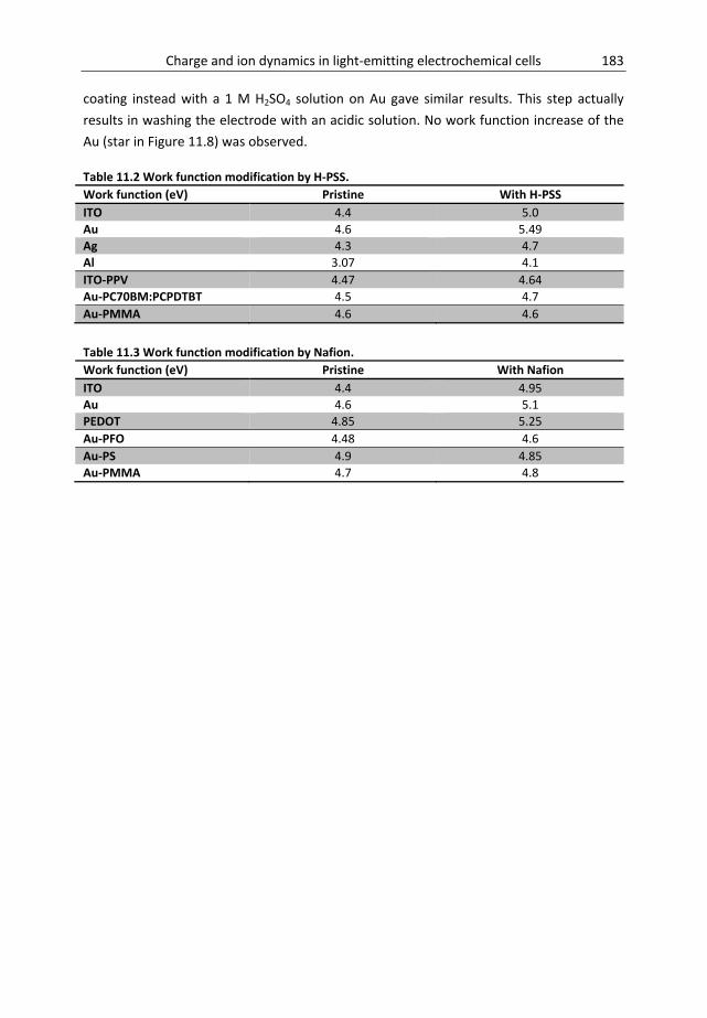
Charge and ion dynamics in light‐emitting electrochemical cells 183
coating instead with a 1 M H2SO4 solution on Au gave similar results. This step actually
results in washing the electrode with an acidic solution. No work function increase of the
Au (star in Figure 11.8) was observed.
Table 11.2 Work function modification by H‐PSS.
Work function (eV) Pristine With H‐PSS
ITO 4.4 5.0
Au 4.6 5.49
Ag 4.3 4.7
Al 3.07 4.1
ITO‐PPV 4.47 4.64
Au‐PC70BM:PCPDTBT 4.5 4.7
Au‐PMMA 4.6 4.6
Table 11.3 Work function modification by Nafion.
Work function (eV) Pristine With Nafion
ITO 4.4 4.95
Au 4.6 5.1
PEDOT 4.85 5.25
Au‐PFO 4.48 4.6
Au‐PS 4.9 4.85
Au‐PMMA 4.7 4.8

184 Chapter 11 | Origin of work function modification by electrolytes
Figure 11.8 Work function as measured by SKPM for substrates covered by 10 nm H‐PSS or Nafion. Substrates are categorized in clean conductors (black circles or pentagons for H‐PSS and Nafion, respectively) and metals coated with a 5 – 10 nm thick film of semiconductor (blue squares or diamonds for H‐PSS and Nafion, respectively) or insulator (red triangles for Nafion). The symbol filling indicates the specific substrate material as shown in the legend. The horizontal lines indicate the average change in work function for each substrate category. The data is also presented in Table 11.2 and Table 11.3.
The results regarding PFN, H‐PSS and Nafion shown in Figure 11.3 and Figure 11.8 show
that despite using different materials, the work function modification behaves the same,
dependent on the type of substrate used. Different is however the sign of the work
function modification as PFN reduces the substrate work function, whereas H‐PSS and
Nafion enhance it. According to the proposed mechanism for PFN, the direction of the
dipole in the WML at the interface is determined by the size of the constituent parts and
their ability to move. In the anionic polyelectrolytes studied here the charged constituent
parts are the ions within the SO3−H+ group. As the SO3
− ion is covalently bound to a
polymer backbone, it has more difficulty in reaching the interface than the small, ionically
bound proton. Therefore mainly the proton approaches the interface, resulting in a dipole
oriented towards the interface. These results therefore demonstrate that the proposed
mechanism does not only apply to the work function modification by PFN, but also by
polyelectrolytes like Nafion or H‐PSS.
11.3.5 IonsizeeffectsinWMLsAccording to our proposed mechanism (Figure 11.6) the geometrical size of the charged
constituents should strongly affect the size and direction of the induced interfacial dipole.
To verify whether the ion size influences the magnitude of the work function modification,
the work function modification by X+PSS− with X+ = H+, Li+, Na+ was studied on Au. In

Charge and ion dynamics in light‐emitting electrochemical cells 185
addition the work function modification by quaternized ammonium salts was studied as
well: a series of tetrabutylammonium halides, (TBA+Y−) with Y− = F−, Cl−, Br−, I−; and salts
(TBA+Z−) with Z− = BH4−, BF4
−, PF6−. Also the size of the alkyl group (methyl, butyl, or hexyl)
in the ammonium ion was varied. The work function modification of Au by deposition of
thin layers of approximately 10 nm is shown in Figure 11.9 as a function of the ion radius.
The ionic radii were taken from literature.43‐46 The radius of the ion with an underlined
name is connected to the horizontal axis. The general trend that is observed in all three
series (X+PSS−; TBA+Y−; TBA+Z−) is that an increase in ion size is accompanied by a reduction
in the magnitude of the work function modification. In H+PSS− a work function increase is
observed as the PSS‐ ion has a low movability due to its large relative size. Increasing the
size of the positive counterion reduces this difference and clearly results in a reduced
magnitude of the work function change. In the TBA+F− and TBA+BH4− salts, the TBA+ ion has
the lowest movability compared to the counterions due to the four relatively large butyl
chains. Consequently a work function reduction is expected and also observed in Figure
11.9. Increasing the size of the counterions again reduces the difference in movability. The
experiment is in agreement with this as the magnitude of the work function reduction is
reduced. That not only the ion‐size is important regarding work function modification is
illustrated by the stronger reduction in case the larger BH4‐ ion is used opposed to F‐, Cl‐,
or Br‐. Clustering and ordering of the salt molecules, which can strongly vary between the
different series, is likely to play a large role as well. This is in line with earlier observations
by Yang et al.,47 where polyelectrolytes with larger ions used as interlayer were found to
result in better in device performance. Furthermore, it should be noted that in devices,
the performance is not only determined by the work function change due to a WML, but
also by additional effects of the WML on electrical transport and injection. A change in
magnitude of the ammonium constituent itself leads however to an oppositely expected
effect: c.f. TMA+I− vs. TBA+I− and TBA+Br− vs. THA+Br− (see Figure 11.2i‐k for the structural
formulae). This may tentatively be explained by a change in salt density at the interface or
the ability to block the counter ions from reaching the surface. Regarding the sign of the
work function modification by the ammonium series, it is found to be opposite to the PSS−
series. This corresponds to a dipole orientation such that the largest ion, PSS− and TBA+, is
the furthest away from the interface and the smaller counter ion is closest.
The dashed purple line in Figure 11.9 illustrates the work function modification by PFN to
enable comparison with the polyelectrolytes. The work function reduction by PFN is
similar in case TBA+F− is used. If however TBA+PF6− is used, no work function reduction is
observed. The latter was also observed in Ref. 13, where the work function modification
by PEIE was measured as a function of the acidity of the solution from which it was
deposited. The largest work function modification was obtained from a basic solution
when PEIE with neutral amine groups was present. When using an acidic solution, by

186 Chapter 11 | Origin of work function modification by electrolytes
addition of H+PF6
−, part of the amines is protonated and electrostatically compensated by
a PF6‐ counterion. In that case the magnitude of the work function modification was
observed to decrease. This is in line with our measurement of TBA+PF6− on Au shown in
Figure 11.9 where no work function modification is observed.
Figure 11.9 Work function of an Au substrate covered by a thin layer (5‐10 nm) of salt as measured by SKPM. The labels show the type of ion and the ion radius of the underlined ion corresponds to the horizontal axis. The dashed lines indicate the work function of a clean Au substrate and an Au substrate covered with PFN.
11.4 GeneralconsiderationsThe general behavior of the interlayers described in the previous paragraphs allows a
consistent description of the work function changes, but we note that these can be
accompanied with effects which are specific for the materials used. For example, work
function reduction by PFN on P3HT is expected but not observed experimentally. We
tentatively attribute this to material specific effects that may be superimposed on, or
interfere with the interface dipole formation as discussed in this chapter. It is known for
example that PFN in combination with fullerenes results in doping of the fullerenes.20
Another example is found in a recent paper by Wetzelaer et al.,48 where an anionic
electrolyte, stearate, with a relatively large counter ion, Cs+, was shown to improve
electron injection from Al to a comparable level as Ba. This result may be explained by the
relatively large size of the Cs+ ion which might make image charge screening of the
negatively charged polymer more favorable. Alternatively, n‐type doping by Cs+ may
explain the observed results as well in this specific case.49
In actual devices, where WMLs are typically sandwiched between an organic
semiconductor and a metallic electrode, the situation is more complicated than the one
studied here. In lowest order, oppositely directed dipoles are expected at both interfaces
0.0 0.5 1.0 1.5 2.0 2.5 3.0
5.5
5.0
4.5
4.0TMA-I
TBA-PF6
TBA-BF4
TBA-BH4
THA-Br
TBA-I
TBA-BrTBA-Cl
TBA-F
PFN
Na-PSS
Li-PSS
H-PSS
Wor
kfun
ctio
n (e
V)
Ion radius (Å)
Au

Charge and ion dynamics in light‐emitting electrochemical cells 187
of the WML. Typically, the metal‐WML interface dipole will be largest and improved
injection may still be expected. However, the presence of substantial space charge in the
semiconductor may destabilize the interfacial dipoles. Injection of electrons (holes) and
the consequent formation of negative (positive) space charge in the organic
semiconductor can destabilize a dipole pointed away from (towards) the semiconductor.
This would be an interesting topic for further study.
11.5 ConclusionIn summary we have shown that WMLs based on tertiary aliphatic amines and
polyelectrolytes, e.g. sulfonic acid based polymers or aliphatic quaternized ammonium
salts, show similar behavior in work function modification. Work function modification
occurs only on (semi‐)conducting substrates and is independent of the substrate work
function in the range of 3 to 5 eV. Additionally the work function modification does not
depend on the WML thickness, but does depend on the relative size of the anion and
cation and their respective ability to move.
The data supports a single mechanism for both work function reduction and enhancement
by prompted formation of an interfacial dipole. This process is driven by the attraction of
the positive and negative part of the dipole towards the interface by the image charge
interaction in case the substrate is a (semi‐)conductor. The geometrical size and
movability of the positive and negative parts of the dipole determine which (partial)
charge can get closest to the substrate, resulting in a net dipole orientation away from or
towards the interface which modifies the work function. The large data set proves that the
general work function modification by the WMLs studied here cannot be described by any
doping mechanism, charge transfer, or spontaneous dipole orientation in the solid film
after deposition. Although other mechanisms are not excluded for specific interlayer‐
substrate combinations, the prompted dipole formation mechanism is found to be
universal for a large variety of interlayer materials deposited on a large variety of
substrates and provides a guideline for developing new materials.

188 Chapter 11 | Origin of work function modification by electrolytes
References
[1] F. Huang, H. B. Wu, D. Wang, W. Yang, Y. Cao, Chem. Mater. 16 (2004) 708.
[2] A. K. K. Kyaw, D. H. Wang, V. Gupta, J. Zhang, S. Chand, G. C. Bazan, A. J. Heeger, Adv. Mater. 25
(2013) 2397.
[3] C. M. Zhong, C. H. Duan, F. Huang, H. B. Wu, Y. Cao, Chem. Mater. 23 (2011) 326.
[4] L. F. Lan, J. B. Peng, M. L. Sun, J. L. Zhou, J. H. Zou, J. Wang, Y. Cao, Org. Electron. 10 (2009) 346.
[5] C. V. Hoven, R. Q. Yang, A. Garcia, V. Crockett, A. J. Heeger, G. C. Bazan, T. Q. Nguyen, Proc. Natl. Acad.
Sci. U S A 105 (2008) 12730.
[6] J. H. Seo, T. Q. Nguyen, J. Am. Chem. Soc. 130 (2008) 10042.
[7] J. Lee, H. Kang, J. Kong, K. Lee, Adv. Energy Mater. 4 (2014) 1301226.
[8] S. Braun, W. R. Salaneck, M. Fahlman, Adv. Mater. 21 (2009) 1450.
[9] H. Vazquez, F. Flores, A. Kahn, Org. Electron. 8 (2007) 241.
[10] A. Kahn, N. Koch, W. Y. Gao, J. Polym. Sci. Part B Polym. Phys. 41 (2003) 2529.
[11] L. Lindell, M. P. de Jong, W. Osikowicz, R. Lazzaroni, M. Berggren, W. R. Salaneck, X. Crispin, J. Chem.
Phys. 122 (2005) 84712.
[12] D. E. Gardin, G. A. Somorjai, J. Phys. Chem. 96 (1992) 9424.
[13] Y. H. Zhou, C. Fuentes‐Hernandez, J. Shim, J. Meyer, A. J. Giordano, H. Li, P. Winget, T. Papadopoulos,
H. Cheun, et al., Science 336 (2012) 327.
[14] F. Huang, H. B. Wu, Y. Cao, Chem. Soc. Rev. 39 (2010) 2500.
[15] R. D. Xia, D. S. Leem, T. Kirchartz, S. Spencer, C. Murphy, Z. C. He, H. B. Wu, S. J. Su, Y. Cao, et al., Adv.
Energy Mater. 3 (2013) 718.
[16] S. Liu, K. Zhang, J. Lu, J. Zhang, H.‐L. Yip, F. Huang, Y. Cao, J. Am. Chem. Soc. 135 (2013) 15326.
[17] Y.‐H. Kim, T.‐H. Han, H. Cho, S.‐Y. Min, C.‐L. Lee, T.‐W. Lee, Adv. Funct. Mater. 24 (2014) 3808.
[18] F. Lui, Z. A. Page, V. V. Duzhko, T. P. Russell, T. Emrick, Adv. Mater. 25 (2013) 6868.
[19] B. H. Lee, I. H. Jung, H. Y. Woo, H.‐K. Shim, G. Kim, K. Lee, Adv. Funct. Mater. 24 (2014) 1100.
[20] C.‐Z. Li, C.‐C. Chueh, F. Ding, H.‐L. Yip, P.‐W. Liang, X. Li, A. K. Y. Jen, Adv. Mater. 25 (2013) 4425.
[21] T. W. Lee, O. Kwon, M. G. Kim, S. H. Park, J. Chung, S. Y. Kim, Y. Chung, J. Y. Park, E. Han, et al., Appl.
Phys. Lett. 87 (2005) 231106.
[22] T. W. Lee, Y. Chung, O. Kwon, J. J. Park, Adv. Funct. Mater. 17 (2007) 390.
[23] M. Manceau, S. Berson, Nanotechnology 25 (2014) 014018.
[24] G. Greczynski, T. Kugler, M. Keil, W. Osikowicz, M. Fahlman, W. R. Salaneck, J. Electron. Spectrosc.
Relat. Phenom. 121 (2001) 1.
[25] A. M. Nardes, M. Kemerink, M. M. de Kok, E. Vinken, K. Maturova, R. A. J. Janssen, Org. Electron. 9
(2008) 727.
[26] K. Zilberberg, S. Trost, H. Schmidt, T. Riedl, Adv. Energy Mater. 1 (2011) 377.
[27] J. Meyer, K. Zilberberg, T. Riedl, A. Kahn, J. Appl. Phys. 110 (2011).
[28] J. Lim, M. Park, W. K. Bae, D. Lee, S. Lee, C. Lee, K. Char, ACS Nano 7 (2013) 9019.
[29] Q. B. Pei, G. Yu, C. Zhang, Y. Yang, A. J. Heeger, Science 269 (1995) 1086.
[30] S. van Reenen, P. Matyba, A. Dzwilewski, R. A. J. Janssen, L. Edman, M. Kemerink, J. Am. Chem. Soc.
132 (2010) 13776.
[31] M. Lenes, G. Garcia‐Belmonte, D. Tordera, A. Pertegas, J. Bisquert, H. J. Bolink, Adv. Funct. Mater. 21
(2011) 1581.
[32] K. Abbas, D. Marji, Z. Naturforsch. A 60 (2005) 667.

Charge and ion dynamics in light‐emitting electrochemical cells 189
[33] P. C. Rusu, G. Giovannetti, C. Weijtens, R. Coehoorn, G. Brocks, Phys. Rev. B 81 (2010) 125403.
[34] H. Ishii, K. Sugiyama, E. Ito, K. Seki, Adv. Mater. 11 (1999) 972.
[35] W. C. Meixner, P. R. Antoniewicz, Phys. Rev. B 13 (1976) 3276.
[36] P. R. Hilton, D. W. Oxtoby, J. Chem. Phys. 72 (1980) 6346.
[37] B. L. Maschhoff, J. P. Cowin, J. Chem. Phys. 101 (1994) 8138.
[38] P. M. Dewick, Essentials of Organic Chemistry. John Wiley & Sons: West Sussex, 2006.
[39] R. C. G. Naber, J. Massolt, M. Spijkman, K. Asadi, P. W. M. Blom, D. M. de Leeuw, Appl. Phys. Lett. 90
(2007) 113509.
[40] J. J. Brondijk, K. Asadi, P. W. M. Blom, D. M. de Leeuw, J. Polym. Sci. Part B Polym. Phys. 50 (2012) 47.
[41] P. Wurfel, I. P. Batra, J. T. Jacobs, Phys. Rev. Lett. 30 (1973) 1218.
[42] P. Wurfel, I. P. Batra, Phys. Rev. B 8 (1973) 5126.
[43] A. L. Rohl, D. M. P. Mingos, Dalton Trans. (1992) 3541.
[44] Y. Nakamori, K. Miwa, A. Ninomiya, H. W. Li, N. Ohba, S. I. Towata, A. Zuttel, S. I. Orimo, Phys. Rev. B
74 (2006) 045126.
[45] J. C. Slater, J. Chem. Phys. 41 (1964) 3199.
[46] J. S. Huang, B. G. Sumpter, V. Meunier, Chem. Eur. J. 14 (2008) 6614.
[47] R. Q. Yang, H. B. Wu, Y. Cao, G. C. Bazan, J. Am. Chem. Soc. 128 (2006) 14422.
[48] G. A. H. Wetzelaer, A. Najafi, R. J. P. Kist, M. Kuik, P. W. M. Blom, Appl. Phys. Lett. 102 (2013) 053301.
[49] H. H. P. Gommans, M. Kemerink, G. G. Andersson, R. M. T. Pijper, Phys. Rev. B 69 (2004) 155216 .

190 Chapter 11 | Origin of work function modification by electrolytes

Chapter12 Perspectiveonthefutureof
LECs

192 Chapter 12 | Perspective on the future of LECs
12.1 CurrentviewonoperationalmechanismofLECsGreat effort has been put in understanding, development and improvement of LECs by
researchers dating back until the first report on LECs by Pei et al. in 1995.1 As a result
relatively high efficiencies2‐5 have already been reached from single layer devices which
are ideal for large‐scale, cheap processing methods.6 Nevertheless, incomplete
understanding of LEC device operation has obscured the possibilities and limits of LECs as
well as the best routes to proceed for making the technology successful. The objective of
this thesis was to remove this obscurity by endeavoring to conceptually and quantitatively
understand the dominant processes in LEC operation. Operation starting from carrier
injection, doping/ion dynamics, charge transport, charge recombination until the radiative
exciton decay processes has been investigated by experiments and numerical modeling in
polymer and iTMC based semiconductors.
First we identified that the electrical transport mechanism in polymer LECs is based on
electrochemical doping of the organic semiconductor. A dynamic p‐i‐n junction structure
is formed where light emission originates from the intrinsic region. A prerequisite for the
formation of such a p‐i‐n junction is non‐limited carrier injection, achieved by piling up
ions at the contacts to form electric double layers. N‐type and p‐type doping then results
from redistribution of cations and anions to opposite sides of the active layer to
electrostatically compensate injected electrons and holes. The response time of LECs is
related to this relatively slow ionic redistribution. The latter is however not limited by the
relatively slow mobile ion transport, but rather to the (even) slower process of salt
dissociation into free, mobile ions. The consequences of electrochemical doping on the
electronic transport are the following:
i) Large electronic carrier densities are created in the active layer without the
need to provide large electric fields, effectively improving the conductivity of
the semiconductor;
ii) The electronic carrier mobility is improved significantly by the large doping
density, improving the conductivity in the doped regions even more;
iii) The significantly improved conductivity enables low‐voltage operation of
devices with relatively thick active layers (>>10‐7 m);
iv) The doped regions result in near unity recombination efficiency by
recombination of all carriers at the intrinsic region.
These effects are found to scale with the admixed salt density in the active layer of the
LEC. So to optimize LECs for charge transport, while ignoring the effects of doping on the
radiative efficiency, an as high as possible ion density is preferred, provided electronic
carrier injection can follow the enhanced bulk conductivity. These effects were found to
hold for LECs with relatively small (100 nm) and large (100 µm) active layer thicknesses.

Charge and ion dynamics in light‐emitting electrochemical cells 193
In LECs based on ionic transition metal complexes highly similar electrical transport was
observed despite the large difference in active layer components. N‐type and p‐type
doped regions are also formed during operation, leaving an intrinsic region in between
where the majority of the applied potential drops and where recombination takes place.
To further test the similarity between polymer and iTMC‐LECs the thermal activation of
the turn‐on of both types of devices was studied. The related thermal activation energy
was found to be similar to the thermal activation energy of the ion conduction in the same
device. This further confirms that ion redistribution is linked to the turn‐on of polymer and
iTMC‐LECs, being in line with electrochemical doping during operation.
The tradeoff of the improved charge transport in LECs is a reduction of the luminescent
efficiency by electrochemical doping, which was identified by two separate observations.
Firstly, after switch‐on of polymer and iTMC‐LECs, the luminescent efficiency was found to
roll off. Simultaneously the active layer was electrochemically doped, evidenced by a
continuous enhancement of the current density and brightness of the LECs. Secondly, for
polymer LECs in steady‐state operation, an enhanced doping density was found to reduce
the luminescent efficiency. The doping density was enhanced by admixing additional salt
in the active layer. To explore the origin of the reduced luminescent efficiency, polaron‐
induced photoluminescence quenching was studied in conjugated polymers for varying
doping density. Both Förster resonance energy transfer and charge transfer were
determined as quenching mechanisms. The found quenching model was inserted in a
numerical device model which reproduced qualitatively and quasi‐quantitatively the
reduction in luminescent efficiency in transient and steady‐state operation. This proves
that unlike the electrical transport, the luminescent efficiency is negatively affected by
electrochemical doping which quenches the formed excitons. The optimal (polymer) LEC
will therefore necessarily require a compromise between transport and recombination
optimization.
Investigation of magnetic field effects on electrical transport and luminance in LECs
showed that triplet excitons can improve both charge transport and luminescent
efficiency. A large magneto‐resistance of 12 % in fully doped LECs is explained by triplet
excitons detrapping electrical charge carriers. Furthermore a reduction in magneto‐
efficiency is related to triplet‐triplet annihilation, which is an additional source of singlet
excitons. The contribution of delayed fluorescence to the total light output of the LEC is
estimated to be roughly 10‐20 %.
Besides electrochemical doping, thin films of electrolytes were furthermore observed to
be able to enhance or reduce electrode work functions. This work function modification
was found to be independent of the electrolyte layer thickness and work function of the
electrode and dependent on the dielectric properties of the substrate on which it is

194 Chapter 12 | Perspective on the future of LECs
deposited. This excludes possible mechanisms like charge transfer, electric double layer
formation or spontaneous dipole orientation. The work function modification can,
however, be described by dipole orientation at the interface induced by image charges of
the electrolyte itself in the substrate. A requirement for this process to occur is asymmetry
in size or side‐groups of the oppositely charged constituents of the electrolyte.
The charge transport, recombination and radiative decay characteristics in LECs were
successfully modeled by our numerical device model. Quasi‐quantitative and qualitative
agreement between experiments and simulations based on experimentally determined
input parameters, proves that the basic processes for LEC operation are known and
relatively well understood. Therefore we conclude that the combined use of ionic
conductors and organic semiconductors in LECs enables great improvement of electrical
transport and brightness at the cost of a reduced luminescent efficiency.
12.2 FuturedirectionstoimproveLECsThe future and success of LECs to become a significant, global lighting technology highly
depends on developments to improve the luminescent efficiency, response time and
lifetime without significant compromises in the current advantages in processing and
electrical transport. Below, the perspective of the author is given on possible future
developments to improve the performance of LECs.
12.2.1 EmissionengineeringTo be able to take full advantage of the enhanced electrical transport in LECs and the
concomitant brightness, the strong reduction in efficiency needs to be prevented. To
address the root of the cause, exciton quenching must be avoided. Requirements for
effective polaron‐induced exciton quenching are i) exciton formation near a high density
of polarons, ii) exciton diffusion, iii) spectral overlap for exciton emission and polaron
absorption, and iv) a sufficient exciton lifetime. To avoid exciton quenching one or more of
these requirements should not be fulfilled.
The use of dyes for light emission gives an opportunity to prevent exciton diffusion and/or
spectral overlap between excitons and polarons. In case the dye has a lower bandgap
compared to its host system, excitons can be energetically trapped in the dye, reducing
exciton diffusion. As diffusion was found to be a main contributor to the quenching
process, this could strongly reduce exciton quenching and enable the use of higher doping
densities. The addition of large side‐groups on such dyes7 may furthermore enhance the
distance between neighboring sites, to further reduce the probability of quenching.
Especially regarding iTMC‐LECs host‐guest systems have already been reported.8‐10 Issues
that may arise in such host‐guest systems are for example unwanted emission from the
host material11 or asymmetrical carrier trapping. The latter may lead to imbalanced carrier

Charge and ion dynamics in light‐emitting electrochemical cells 195
transport, resulting in carrier recombination close to one of the electrodes where exciton
quenching is relatively strong. Nevertheless, given the strong contribution of exciton
quenching in polymer LECs, a recent promising report12 and the fact this topic remains a
relatively unexplored, dyes in LECs are highly promising to prevent exciton quenching and
boost the luminescent performance. It furthermore solves the problem of synthesis of a
single material with good transport and light emission properties.
Another method to reduce quenching is by enhancement of the radiative decay rate of
excitons. By synthesis and selection of materials with an enhanced radiative decay rate,
the contribution of the competing quenching process can be reduced. The radiative decay
rate of singlet excitons can be determined from the Strickler‐Berg relation.13 A high
dielectric constant and strong absorption at the relevant fluorescence wavelengths are
required for a high decay rate, which is not so easily improved in typically low dielectric
organic semiconductors like PPV. Enhancement of the dielectric constant may however
improve the decay rate.
The radiative decay rate can also be enhanced by improving the fraction of the excitons
with a singlet state. Our study on OMAR in PPV‐based LECs proved that this fraction is
worse than 0.25. Better understanding and control of the processes determining the final
singlet exciton fraction should be able to lift it to 0.25 and perhaps beyond. Such a route is
currently little explored in the field, but also not likely to be a short‐term winner to
improve the efficiency.
A more viable route is to turn the attention to triplet emitters, which have enhanced
luminescent efficiency as all excitons can undergo radiative decay.14 Although triplet
emission in LECs is not new –iTMC‐LECs based on iridium exhibit triplet emission‐ the
origin of quenching is still relatively unexplored. We15 and others16 have shown that also
here a roll‐off in efficiency occurs, which is due to exciton quenching. This quenching likely
takes place via a combination of triplet‐triplet annihilation and triplet‐polaron quenching.
Both processes can be reduced by enhancement of the radiative decay rate. Haneder et al.
reported that regarding triplet emitters, besides spin‐orbit coupling between the excited
T1 and S1 states, a small singlet‐triplet splitting between T1 and S1 (ΔEST) results in an
enhanced radiative decay rate.17 A small splitting is for example the case in iridium
complexes and strongly depends on the ligands. Further enhancement of the radiative
triplet exciton decay rate by specially designed materials18 will help to reduce these
quenching effects and may therefore be a promising route.
12.2.2 ReducingtheresponsetimeAnother issue which requires attention is the relatively long response time in LECs, related
to the slow redistribution of ions. Two approaches are reported in literature, being the use

196 Chapter 12 | Perspective on the future of LECs
of a dedicated driving scheme for operation or fixation of doping during a pre‐treatment
of the LEC.
Attempts to fix doping are most notably by use of chemical reactions19‐22 or the strong
temperature dependence of the ion mobility.23‐25 In either case the device is prebiased to
allow ions to redistribute over the device forming a p‐i‐n junction. The doping can then be
fixed by either lowering of the temperature or chemical reactions with (side‐groups of) the
ionic compounds. After removal of the bias the doping remains in place. Subsequent
application of a bias voltage should then not result in ion transport to form new doping
complexes. If that is the case, then the turn‐on time depends solely on the response of the
relatively mobile electronic carriers.
An alternative method to speed up the electrochemical doping process is by application of
a larger driving voltage. Driving schemes26‐27 in which an initial, large bias voltage is used
can therefore significantly speed up the doping in the device to quickly reach quasi‐
steady‐state operation. Use of a constant current driving scheme is an even more elegant
solution.27‐28
Another, rather unexplored method is to address the intrinsic cause of the slow response
speed, i.e. the slow salt dissociation in the active layer.29 The salt dissociation rate
depends on the binding energy between the ions and the ion capture rate. The latter is
likely related to the ion mobility. Reduction of the salt binding energy and enhancement of
the ion mobility can be achieved by enhancement of the dielectric constant: the dielectric
constant is inversely proportional to the binding energy (which originates from
electrostatic interaction) between ions. This means that an enhancement of the dielectric
constant from e.g. PPV, 3, to 10 may have significant effect.
To enhance the dielectric constant, alternative semiconducting materials could be
considered. Note that in electroluminescent devices typically low dielectric materials are
preferred due to the recombination rate being inversely proportional to the dielectric
permittivity. In LECs the recombination efficiency is already (near) optimal, which means
that enhancement of the dielectric constant does not necessarily harm the recombination
efficiency. Today such semiconductors are mainly used for photovoltaic applications
where recombination should be suppressed.30‐31 It should be noted that the relative
dielectric constant of PEO, the material typically used to promote salt dissociation and ion
mobility in LECs, is 6.32
An additional advantage of the use of a high dielectric semiconductor is that the addition
of PEO may no longer be required. Exclusion of PEO from the active layer would solve
issues like phase separation, which likely has an effect on the current lifetime of LECs.33

Charge and ion dynamics in light‐emitting electrochemical cells 197
Furthermore it would enable admixture of additional components like dyes in the active
layer without creating a 4‐component system.
The use of alternative salts may also be a possibility to reduce the response time. The
binding energy is inversely proportional to the ionic bond length, so larger ions will likely
have a smaller binding energy. This may, however, tradeoff in mobility as larger ions are
more difficult to be transported through solid media.

198 Chapter 12 | Perspective on the future of LECs
References
[1] Q. B. Pei, G. Yu, C. Zhang, Y. Yang, A. J. Heeger, Science 269 (1995) 1086.
[2] T. Hu, L. He, L. Duan, Y. Qiu, J. Mater. Chem. 22 (2012) 4206.
[3] Y. P. Jhang, H. F. Chen, H. B. Wu, Y. S. Yeh, H. C. Su, K. T. Wong, Org. Electron. 14 (2013) 2424.
[4] S. Tang, J. Pan, H. A. Buchholz, L. Edman, J. Am. Chem. Soc. 135 (2013) 3647.
[5] Y. Yang, Q. B. Pei, J. Appl. Phys. 81 (1997) 3294.
[6] A. Sandström, H. F. Dam, F. C. Krebs, L. Edman, Nat. Commun. 3 (2012) 1002.
[7] R. D. Costa, E. Orti, H. J. Bolink, S. Graber, C. E. Housecroft, E. C. Constable, Adv. Funct. Mater. 20
(2010) 1511.
[8] A. R. Hosseini, C. Y. Koh, J. D. Slinker, S. Flores‐Torres, H. D. Abruna, G. G. Malliaras, Chem. Mater. 17
(2005) 6114.
[9] C. T. Liao, H. F. Chen, H. C. Su, K. T. Wong, Phys. Chem. Chem. Phys. 14 (2012) 1262.
[10] A. Pertegas, N. M. Shavaleev, D. Tordera, E. Orti, M. K. Nazeeruddin, H. J. Bolink, J. Mater. Chem. C 2
(2014) 1605.
[11] S. Coe, W. K. Woo, M. Bawendi, V. Bulovic, Nature 420 (2002) 800.
[12] G. Qian, Y. Lin, G. Wantz, A. R. Davis, K. R. Carter, J. J. Watkins, Adv. Funct. Mater. (2014).
[13] S. J. Strickler, R. A. Berg, J. Chem. Phys. 37 (1962) 814.
[14] F. C. Chen, Y. Yang, Q. Pei, Appl. Phys. Lett. 81 (2002) 4278.
[15] S. van Reenen, T. Akatsuka, D. Tordera, M. Kemerink, H. J. Bolink, J. Am. Chem. Soc. 135 (2013) 886.
[16] S. B. Meier, D. Hartmann, D. Tordera, H. J. Bolink, A. Winnacker, W. Sarfert, Phys. Chem. Chem. Phys.
14 (2012) 10886.
[17] S. Haneder, E. Da Como, J. Feldmann, J. M. Lupton, C. Lennartz, P. Erk, E. Fuchs, O. Molt, I. Munster, et
al., Adv. Mater. 20 (2008) 3325.
[18] Q. Wang, I. W. H. Oswald, M. R. Perez, H. P. Jia, B. E. Gnade, M. A. Omary, Adv. Funct. Mater. 23
(2013) 5420.
[19] C. V. Hoven, H. P. Wang, M. Elbing, L. Garner, D. Winkelhaus, G. C. Bazan, Nat. Mater. 9 (2010) 249.
[20] S. Tang, L. Edman, Electrochim. Acta 56 (2011) 10473.
[21] J. M. Leger, D. B. Rodovsky, G. R. Bartholomew, Adv. Mater. 18 (2006) 3130.
[22] C. H. W. Cheng, M. C. Lonergan, J. Am. Chem. Soc. 126 (2004) 10536.
[23] J. Gao, G. Yu, A. J. Heeger, Appl. Phys. Lett. 71 (1997) 1293.
[24] J. Gao, Y. F. Li, G. Yu, A. J. Heeger, J. Appl. Phys. 86 (1999) 4594.
[25] J. H. Shin, S. Xiao, A. Fransson, L. Edman, Appl. Phys. Lett. 87 (2005) 043506.
[26] G. Yu, Y. Cao, C. Zhang, Y. F. Li, J. Gao, A. J. Heeger, Appl. Phys. Lett. 73 (1998) 111.
[27] J. F. Fang, P. Matyba, L. Edman, Adv. Funct. Mater. 19 (2009) 2671.
[28] D. Tordera, S. Meier, M. Lenes, R. D. Costa, E. Orti, W. Sarfert, H. J. Bolink, Adv. Mater. 24 (2012) 897.
[29] L. Holzer, F. P. Wenzl, S. Tasch, G. Leising, B. Winkler, L. Dai, A. W. H. Mau, Appl. Phys. Lett. 75 (1999)
2014.
[30] M. Lenes, F. B. Kooistra, J. C. Hummelen, I. Van Severen, L. Lutsen, D. Vanderzande, T. J. Cleij, P. W. M.
Blom, J. Appl. Phys. 104 (2008) 114517.
[31] X. Liu, K. S. Jeong, B. P. Williams, K. Valchshouri, C. H. Guo, K. Han, E. D. Gomez, Q. Wang, J. B. Asbury,
J. Phys. Chem. B 117 (2013) 15866.
[32] A. Munar, A. Sandstrom, S. Tang, L. Edman, Adv. Funct. Mater. 22 (2012) 1511.
[33] X. Y. Li, J. Gao, G. J. Liu, Org. Electron. 14 (2013) 2711.

Appendix

200 Appendix A | Numerical device model
A NumericalmodeltodescribeoperationofLECsTo model the device operation of light‐emitting electrochemical cells a numerical model is
used which describes carrier injection, transport and recombination in the active layer in
the presence of mobile ions.1‐3 Two similar versions of the model were used, a 1D version
based on the drift‐diffusion equations and a 2D version based on the Boltzmann transport
equation. Both models solve the carrier transport equations for electrons, holes, anions
and cations, and Poisson’s equation by forward integration in time. In the next paragraphs
a detailed description is given of the methods to describe charge transport, carrier
injection and carrier recombination. Additional, optional processes like i) a doping
dependence in the carrier mobility, ii) a binding energy between the ions and iii) exciton
quenching were included in the numerical model as well for part of the simulations
presented in this thesis. Parameters that need to be defined for each calculation are
shown in Table A.1.
TableA.1Inputparametersforthenumericalmodelofa light‐emittingelectrochemicalcell.Parameter Symbol
Mobility (electron/hole/anion/cation) µn / µp / µa / µcHOMO and LUMO of semiconductor EHOMO / ELUMO Density of states of semiconductor N0 Salt density c0 Work function of contacts Drain voltage Vbias Temperature T Relative dielectric constant εr
A.1 ChargetransportIn the 1D model, transport of electrons, holes, anions and cations is described by the drift‐
diffusion equations:
, (A.1)
, (A.2)
, (A.3)
, (A.4)
where J and µ refer to the current density and mobility of the charge carriers. n, p, a and c
refer to electron, hole, anion and cation density, respectively, and as well denote the type
of charge carrier when used as subscript. The electron and hole mobility could be chosen
Charge and ion dynamics in light‐emitting electrochemical cells 201
either dependent or independent of the doping density as described in the main text. q is
the absolute electron charge, V is the electrostatic potential, k is Boltzmann’s constant
and T is the temperature. Einstein’s relation between the diffusion constant and the
mobility is assumed to hold. The ion current is zero at the electrodes, for the electrodes
are ionically blocking. Electron and hole injection is explained in detail in Appendix A.2.
The continuity equations are
, (A.5)
, (A.6)
, (A.7)
, (A.8)
for electrons, holes, anions and cations, respectively. Here R is the recombination rate
which is discussed in Appendix A.5. The potential profile throughout the device is
calculated from Poisson’s equation:
, (A.9)
where ε0 and εr are the dielectric and the relative dielectric constant, respectively.
In the 2D model a rectangular grid is used with grid points at the corners of each cell. The
areas of the cells are determined by the widths of the columns and rows which can be
specified per row or column. For each cell a material type is specified, either gate, contact,
dielectric or semiconductor. Calculations of current, recombination, etc. are performed on
the grid points. The four cells surrounding the grid point are in equilibrium with each
other, which is effectuated by area‐average weighting. Consequently, a single quasi Fermi
level is defined on each grid point.
Carrier transport is described by the following Boltzmann transport equations:
, , (A.10)
where , is the quasi Fermi energy for electrons (i = n), holes (i = p), anions (i = a), or
cations (i = c) which is given by

202 Appendix A | Numerical device model
, ln , (A.11)
, ln , (A.12)
, ln , (A.13)
, ln , (A.14)
where and and V is the electrostatic potential. The
Poisson and continuity equations as given for the 1D model were also used in the 2D
model to calculate the electrostatic potential and maintain continuity in carrier transport.
A.2 CarrierinjectionTo describe the injection of electrons and holes into the semiconductor, the following
parameters are of importance: the HOMO and LUMO levels of the semiconductor; the
Fermi level of the contacts; the grid point spacing at the interfaces; and the charge carrier
density in the semiconductor at the interface. The injection models used for calculations
reported in this thesis are called ‘Fowler‐Nordheim’,4 ‘Emtage‐O’Dwyer’5 and ‘modified
Boltzmann’. The first assumes injection is mediated by tunneling through a triangular
barrier. A more detailed description of this model as used in the numerical modeling can
be found in Ref. 6. The Fowler‐Nordheim injection model gives the carrier density n at the
electrode as
, (A.15)
exp⁄
, (A.16)
.
, (A.17)
., (A.18)
where m0 is the free electron mass, h is Planck’s constant, is the injection barrier
height, q is the absolute electronic charge and F is the electric field at the contact plane.
The Emtage‐O’Dwyer injection model includes the effect of the image‐potential of the
injected charge carrier which effectively reduces the injection barrier height to ':7

Charge and ion dynamics in light‐emitting electrochemical cells 203
. (A.19)
This injection barrier is subsequently used in a Boltzmann factor to give a boundary
condition for the carrier density n at the electrode as
exp . (A.20)
Relatively short grid point spacing is needed close to the electrodes to avoid
undersampling. Undersampling at the interfaces namely leads to an unphysical reduction
of the charge carrier injection rate for the Fowler‐Nordheim and Emtage‐O’Dwyer
injection models. It namely increases the distance to be overcome by the injected carriers
to reach the first grid point after the contact. The planar LECs studied in this thesis have an
interelectrode spacing of e.g. 20 µm. Evasion of undersampling at the interfaces by use of
a small grid point spacing leads to extremely long calculation times: this time scales with
one over the smallest spacing of the numerical mesh to maintain numerical stability. In
optimized LECs2 injection, however, does not limit the current through the LEC. deMello,8
for instance, solved this issue by making use of an adaptive‐grid method‐of‐lines. In this
thesis another solution was chosen by designing another injection model: the ‘modified
Boltzmann’ injection model. It uses a Boltzmann factor to describe injection in the
following manner taking into account the band bending just behind the first grid point:
1 exp , (A.21)
where n(1) is the electron density at the first grid point next to the electrode and V(i) the
potential at grid point i (= 1, 2). Hence, the Boltzmann factor is effectively evaluated at the
2nd grid point. The potential at the first grid point V(1) is taken as a boundary condition for
the potential and is thus constant, i.e. 0 or Vbias. The potential at the neighboring grid point
however changes due to space‐charge accumulated at the EDLs which facilitates injection
of electron or holes. In this model injection is not affected by the grid point spacing and
thus thicker devices can be simulated while not having to alter the number of grid points
because of injection problems.
Simulations have been performed proving that all three injection models converge to the
same result if small enough grid point spacing is chosen, i.e. 1 100/80 nm in
this case. The results are shown in Figure A.1. All relevant properties of the LEC are
basically identical for the different injection models in these simulations. By increasing the
grid point spacings for some of the injection models, e.g. Fowler‐Nordheim tunneling
injection, the injection rate becomes limited as shown in Chapter 2.2 However, the results
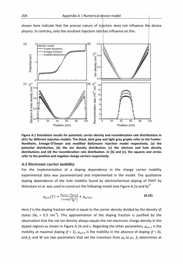
204 Appendix A | Numerical device model
shown here indicate that the precise nature of injection does not influence the device
physics. In contrary, only the resultant injection rate has influence on this.
Figure A.1 Simulation results for potential, carrier density and recombination rate distributions in LECs for different injection models. The black, dark gray and light gray graphs refer to the Fowler‐Nordheim, Emtage‐O’Dwyer and modified Boltzmann injection model respectively. (a) the potential distribution, (b) the ion density distribution, (c) the electron and hole density distributions and (d) the recombination rate distribution. In (b) and (c), the squares and circles refer to the positive and negative charge carriers respectively.
A.3 ElectroniccarriermobilityFor the implementation of a doping dependence in the charge carrier mobility
experimental data was parameterized and implemented in the model. The qualitative
doping dependence of the hole mobility found by electrochemical doping of P3HT by
Shimotani et al. was used to construct the following model (see Figure A.2a and b):9
// , / ,
/ , . (A.22)
Here f is the doping fraction which is equal to the carrier density divided by the density of
states (N0 = 0.3 nm‐3). This approximation of the doping fraction is justified by the
observation that the net ion density always equals the net electronic charge density in the
doped regions as shown in Figure A.1b and c. Regarding the other parameters, µp/n,1 is the
mobility at maximal doping (f = 1), µp/n,0 is the mobility in the absence of doping (f = 0),
and f0 and W are two parameters that set the transition from µ0 to µ1: f0 determines at
-2
-1
0
Pot
entia
l (eV
)
injection model: Fowler-Nordheim Emtage-O'Dwyer modified Boltzmann
0.0
0.2
0.4
0.6
Ion
de
nsi
ty (
nm
- 3)
0 20 40 60 80 1000.0
0.2
0.4
0.6
Ele
ctro
n &
hol
e d
ens
ity (
nm
-3)
Position (nm)
0 20 40 60 80 1000
2
4
6
8
10
12
14
Rec
om
bin
atio
n r
ate
(10
-6 n
m-3
)
Position (nm)
(a) (b)
(c) (d)

Charge and ion dynamics in light‐emitting electrochemical cells 205
which doping fraction the mobility increases and W determines the range of doping
fractions over which this increase occurs.
Figure A.2 The electron/hole mobility as a function of the doping fraction or density. Experimentally determined graphs are shown in (b) for regioregular P3HT9 and in (d) for Super Yellow PPV. Modeled graphs are shown in (a) based on Equation (A.22) and (c) based on Equation (A.23) for the parameters in the inset tables.
The qualitative doping dependence of the carrier mobility in PPV (see Figure A.2d) can be
described by the following model:
/ / , ∙ , (A.23)
where A, B and C are the parameters. In Figure A.2c a plot of this model is shown for A =
‐1∙10‐11, B = 7.2∙10‐10 and C = 0.167, as well as the doping density dependence measured in
Super yellow PPV (see Figure 8.8b).
An optional field dependence of the carrier mobility is assumed to follow Poole‐Frenkel
behavior with exponential factor γ in m0.5 V‐0.5.10‐11 It is implemented by multiplication of
the mobility by exp γ √ .
10-4 10-3 10-2 10-1 100
100
101
102
103
104
pn / p
n,0
Doping fraction
A ‐10‐11
B 7.2∙10‐10
C 0.167
1016 1017 1018 1019 1020 1021
10-12
10-11
10-10
10-9
10-8
SY-PPV electron hole
(m
2 V
-1 s
-1)
Doping density (cm-3)
10-2 10-1 10010-1
100
101
102
103
pn /
pn,0
Doping fraction
10-2 10-1 10010-11
10-10
10-9
10-8
10-7
P3HT hole
(m
2 V
-1 s
-1)
Doping fraction
W 0.04
f0 0.3
µpn,1/µpn,0 102
(a) (b)
(c) (d)

206 Appendix A | Numerical device model
A.4 BindingenergybetweenionsThe binding energy between anions and cations was taken into account by introduction of
a 5th type of carrier: the salt molecule. The binding energy between anion and cation is Es
(>0).
The total anion‐cation binding capture rate Ci (m‐3 s‐1) at each grid point i is
∙ , , ∙ , , , (A.24)
with the capture coefficient (m3 s‐1) and nx,i the density at grid point i for anions (x = a),
cations (x = c), holes (x = p) and electrons (x = n). Note that ions compensated by electrons
or holes do not contribute to formation of salt. To describe dissociation of the salt the
following detrapping rate Ei (m‐3 s‐1) was used:
∙ ∙ , (A.25)
where ns is the salt density, K is the mass action law constant (here taken 1027 m‐3) and the
coefficient is related to the capture coefficient via detailed balance:
∙ . (A.26)
Finally, the net ion binding rate Ui (m‐3 s‐1) is given by
. (A.27)
Before each simulation the device was allowed to reach steady‐state at Vbias = 0 V to allow
salt to form.
A.5 ExcitonformationanddecayIn this model, electron and hole recombination is described by a Langevin process:
. (A.28)
In case the efficiency and luminance of the LEC needs to be calculated, also the decay of
excitons can be included. Recombination of electrons and holes give rise in the model to
singlet and triplet excitons according to a fraction rS and rT. The excitons can subsequently
diffuse with diffusion constant Dexc,S/T. For a given lifetime of the singlet and triplet
excitons, τS and τT, the singlet/triplet rate equations become
, , (A.29)

Charge and ion dynamics in light‐emitting electrochemical cells 207
and
1 , , (A.30)
where S and T are the singlet and triplet exciton densities.
To implement singlet exciton quenching by polarons, a model must be used to describe
the density dependence of the quenching rate kPQ. The exciton quenching can then be
implemented by the definition of
,
∙ , (A.31)
where , is the singlet exciton lifetime in absence of any quenchers. As the numerical
model does not use the molecular sites for calculation but a rectangular grid, quenching
models like Förster resonance energy transfer cannot be simply implemented. The
method to implement exciton quenching by polarons is by use of obtained experimental
data. The doping dependence of ⁄ is measured as shown in Chapter 8,
where kFL = 1 ,⁄ . From this kPQ∙(n+p) can be determined, parameterized and put into the
model to give the quenching rate at each cell at a given polaron density. Excitons on site i
do not interact with excitons on site j ≠ i. Long range interactions are only mediated by the
diffusion of excitons to another cell. As the timesteps in the calculation for charge
transport are typically orders of magnitude larger than the lifetime of the excitons,
and Dexc are reduced by a factor 10‐5, which slows down both processes equally. Such a
delay may give rise to errors in the calculation of the transient behavior of the exciton
decay processes. For transients which are limited by the movement of ions care is taken
that the ion diffusion coefficient Dion = µionkT/q remains smaller than Dexc by at least a
factor 10 to minimize this effect.
A.6 Modeloperation(normalandimpedancemode)In this paragraph the general operation of the models is described. Initially the device only
contains anions and cations which electrostatically compensate each other. No electrons
or holes are present. Only at the contacts electrons and holes are present due to the
boundary conditions imposed by the chosen injection model. In addition, the bias voltage
is applied to one of the contacts, whereas the other contact is set at 0 V. From then on the
model calculates the Fermi energy of all the carriers, followed by solving the Boltzmann
transport equations or the drift‐diffusion equations. Then electron‐hole recombination is
accounted for. Consequently the continuity equations are used to calculate the new
carrier densities at each grid point. A steady‐state solution is obtained when the current,
which is determined by the sum of current through the contacts, becomes constant.

208 Appendix A | Numerical device model
The model also handles impedance measurements. To model the admittance spectrum,
the device is first allowed to reach steady‐state. After this, a voltage step Vstep is applied
and the resulting step response of the current is calculated. The complex admittance
spectra can then be derived by a Fast Fourier Transform of the derivative of the
conductance.

Charge and ion dynamics in light‐emitting electrochemical cells 209
References
[1] S. van Reenen, P. Matyba, A. Dzwilewski, R. A. J. Janssen, A. Edman, M. Kemerink, Adv. Funct. Mater.
21 (2011) 1795.
[2] S. van Reenen, P. Matyba, A. Dzwilewski, R. A. J. Janssen, L. Edman, M. Kemerink, J Am Chem Soc 132
(2010) 13776.
[3] S. van Reenen, R. A. J. Janssen, M. Kemerink, Org. Electron. 12 (2011) 1746.
[4] R. H. Fowler, L. Nordheim, Proc. R. Soc. London Ser. A 119 (1928).
[5] P. R. Emtage, J. J. O'Dwyer, Phys. Rev. Lett. 16 (1966) 356.
[6] A. J. Campbell, D. D. C. Bradley, D. G. Lidzey, J. Appl. Phys. 82 (1997) 6326.
[7] J. J. M. van der Holst, M. A. Uijttewaal, R. Balasubramanian, R. Coehoorn, P. A. Bobbert, G. A. de Wijs,
R. A. de Groot, Phys. Rev. B 79 (2009) 085203.
[8] J. C. deMello, Phys. Rev. B 66 (2002) 235210.
[9] H. Shimotani, G. Diguet, Y. Iwasa, Appl. Phys. Lett. 86 (2005) 022104.
[10] A. R. Buckley, Synth. Met. 160 (2010) 540.
[11] J. Frenkel, Phys. Rev. 54 (1938) 647.

210 Appendix A | Numerical device model

Charge and ion dynamics in light‐emitting electrochemical cells 211
Summary
Charge and ion dynamics in light‐emitting electrochemical cells
Light‐emitting electrochemical cells (LECs) are potential candidates for next‐generation,
low‐cost, large‐area lighting applications. LECs consist of a single, solution‐processed
active layer which contains an organic semiconductor as well as mobile ions. As such, two
classes of LECs can be discerned. Polymer LECs have an active layer which is a blend of a
polymer semiconductor and a solid polymer electrolyte which comprises mobile ions. In
small molecule LECs electronic and ionic transport are enabled by a single material by use
of ionic transition metal complexes (iTMCs). The merits of LECs are excellent processing
characteristics without a large compromise in performance.
Following the first report on LECs by Pei et al. in 1995, researchers have put great efforts
to understand, develop and improve LECs. As a result relatively high efficiencies have
already been reached from single layer devices which are ideal for large‐scale, cheap
processing methods. Nevertheless, incomplete understanding of LEC device operation has
obscured the possibilities and limits of LECs as well as the best routes to proceed for
making the technology successful. The objective of this thesis is to remove this obscurity
by endeavoring to conceptually and quantitatively understand the dominant processes in
LEC operation. Operation starting from carrier injection to doping/ion dynamics, charge
transport, charge recombination until the (non‐)radiative exciton decay processes, has
been investigated by experiments and numerical modeling in polymer and iTMC based
semiconductors.
In Chapters 2‐5 and 6‐7 the electrical transport is studied in LECs based, respectively, on
polymer and iTMC semiconductors. The electrical transport is studied in devices with large
interelectrode gaps of 10‐5 m, enabling characterization by mainly optical and scanning
probe techniques, and in devices with small interelectrode gaps of 10‐7 m, enabling
characterization by electrical techniques. In Chapters 8‐9 the luminescent properties of
polymers in presence of electrochemical doping are investigated. Chapters 10 and 11,
respectively, report on magnetic field effects in LECs and the use of ionic materials as
interlayers in organic electronic devices to improve electrical transport. Below a more
detailed summary is given per chapter.

212 Summary
For a long time two distinct models were used to describe the operational behavior of
LECs: the electrochemical doping model and the electrodynamic model. Both models are
supported by experimental data and numerical modeling in literature. In Chapter 2, we
show that these models are essentially limits of one master model, separated by different
rates of carrier injection. For ohmic non‐limited injection, a dynamic p‐i‐n junction is
formed, which is absent in injection limited devices. This unification is demonstrated by
numerical calculations and measurement of the surface potential, the light emission
profile and the doping profile in operational devices. An analytical analysis yields an upper
limit for the ratio of drift and diffusion currents, having major consequences on the
maximum current density through this type of device.
Incorporation of ions in the active layer of polymer LECs leads to attractive device
properties like enhanced injection and improved carrier transport. In Chapter 3, the effect
of the salt concentration on the operation of LECs is investigated using experiments and
numerical calculations. The current density and light emission are shown to increase
monotonously with increasing ion concentration over a wide range of concentrations. The
increasing current is accompanied by an ion redistribution leading to a narrowing of the
recombination zone. Hence, in absence of detrimental side reactions and doping‐related
electroluminescence quenching the ion concentration should be as high as possible. In
Chapter 9 it will in fact be shown that the latter of these conditions is not fulfilled in
typical LECs.
A major drawback of LECs is the long time scale associated with switching, during which
ions redistribute in the active layer. In Chapter 4, a numerical modeling study is presented
that gives fundamental insight in the dynamics during turn‐on. The characteristic response
of planar LECs to an applied bias is electrochemical doping of the active layer by doping
fronts moving across the active layer. Formation and motion of such doping fronts are
shown to be intimately related to both the electronic and ionic mobility and therefore
provide useful information regarding charge transport in LECs. In particular, it is shown
that the switch‐on time in LECs is directly related to the time an ion needs to cross
approximately half the device, enabling the extraction of the ion mobility from the switch‐
on time.
In Chapter 5, the operational mechanism of polymer LECs in sandwich geometry is studied
by admittance spectroscopy and numerical modeling. Capacitance and conductance at
different frequencies and bias voltages reflect the motion of ions, the formation of electric
double layers, and the formation of a p‐i‐n junction, which is all in line with the
electrochemical doping model. Numerical modeling shows that impedance measurements
cannot be used to determine the actual junction width. In addition, the long settling time
of polymer LECs is shown to be due to a slow process of salt dissociation that continues

Charge and ion dynamics in light‐emitting electrochemical cells 213
after p‐i‐n junction formation, rather than being due to ion conduction. This implies that in
order to significantly decrease the response‐time of LECs an electrolyte/salt combination
with an as low as possible ion binding energy must be used.
In Chapter 6 we switch focus to LECs based on ionic transition metal complexes. Using a
planar electrode geometry, the operational mechanism of iridium(III) iTMC‐based LECs is
studied by a combination of fluorescence microscopy and scanning Kelvin probe
microscopy (SKPM). Application of a bias to the LECs leads to the quenching of the
photoluminescence (PL) in between the electrodes and to a sharp drop of the electrostatic
potential in the middle of the device, far away from the contacts. The results shed light on
the operational mechanism of iTMC‐LECs and demonstrate that these devices work
essentially the same as LECs based on conjugated polymers do, i.e. according to an
electrochemical doping mechanism. Moreover, with proceeding operation time the
potential drop shifts towards the cathode, coincident with the onset of light emission.
During prolonged operation the emission zone and the potential drop both migrate
towards the anode. This event is accompanied by a continuous quenching of the PL in two
distinct regions separated by the emission line.
Two types of LECs are commonly distinguished, the polymer‐based LEC (pLEC) and the
ionic transition metal complex‐based LEC. Apart from marked differences in the active
layer constituents these LEC types typically show operational time scales that can differ by
many orders of magnitude at room temperature. In Chapter 7, we demonstrate that
despite these differences pLECs and iTMC‐LECs show current, light output and efficacy
transients that follow a universal shape. Moreover, we conclude that the turn‐on time of
both LEC types is dominated by the ion conductivity since the turn‐on time exhibits the
same activation energy as the ion conductivity in the off‐state. These results demonstrate
that both types of LECs are really two extremes of one class of electroluminescent devices.
They also implicate that no fundamental difference exists between charge transport in
small molecular weight or polymeric mixed ionic and electronic conductive materials.
Additionally, it follows that the ionic conductivity is responsible for the dynamic properties
of devices and systems using them. This likely extends to mixed ionic and electronic
conductive materials used in organic solar cells and in a variety of biological systems.
An important loss mechanism in organic electroluminescent devices is exciton quenching
by polarons. Gradual electrochemical doping of various conjugated polymer films was
studied in Chapter 8 to determine the doping density dependence of photoluminescence
quenching. Electrochemical doping was achieved by contacting the film with a solid
electrochemical gate and an injecting contact. A sharp reduction in photoluminescence
was observed for doping densities between 1018 and 1019 cm‐3. The doping density
dependence is quantitatively modeled by exciton diffusion in a homogeneous density of

214 Summary
polarons followed by either Förster resonance energy transfer or charge transfer. Both
mechanisms need to be considered to describe polaron‐induced exciton quenching. Thus,
to reduce exciton‐polaron quenching in organic optoelectronic devices, both mechanisms
must be prevented by reducing either exciton diffusion, spectral overlap of the exciton
emission and polaron absorption spectra, doping density, or a combination thereof.
The admixed ions in LECs cause a trade‐off between electrical transport and luminescent
efficiency. Experiments and numerical modeling described in Chapter 9 on thin film LECs
prove that on the one hand carrier injection and transport benefit from electrochemical
doping by mobile ions, whereas on the other hand the electroluminescent efficiency is
reduced by exciton quenching by polarons involved in the doping. As a consequence the
quasi‐steady‐state luminescent efficiency is found to decrease with increasing ion
concentration. The transient of the luminescent efficiency furthermore shows a
characteristic roll‐off while the current still increases, attributed to ongoing
electrochemical doping and the associated quenching. Both effects can be modeled by
exciton polaron‐quenching described by diffusion‐assisted Förster resonance energy
transfer. These results indicate that the tradeoff between efficiency and charge transport
is fundamental in nature, suggesting that the application realm of future LECs should likely
be sought in high‐brightness, low‐production cost devices, rather than in high‐efficiency
devices.
In Chapter 10, magnetic field effects in conductance and electroluminescence are studied
to give insight in spin‐dependent processes. Besides other effects a large negative
magneto‐conductance (MC) of 12% is observed in electrochemically doped LECs at sub‐
bandgap bias voltages. These effects indicate processes like delayed fluorescence from
triplet‐triplet annihilation and spin‐mixing prior to exciton formation. The latter is found to
result in a reduction in triplet exciton density which is argued to reduce detrapping of
polarons in the recombination zone at low bias voltages, explaining the observed negative
MC. Regarding organic magneto‐resistance this study provides novel experimental data to
verify existing models describing magnetic field effects in organic semiconductors which
contribute to better understanding hereof. Furthermore we present indications of strong
magnetic field effects related to interactions between trapped carriers and excitons,
which specifically can be studied in electrochemically doped OLEDs. Regarding LECs, this
work shows that delayed fluorescence from triplet‐triplet annihilation substantially
contributes to the electroluminescence and the device efficiency.
An alternative use of electrolytes, besides in the active layer of LECs, is as thin injection
layers in organic electronics. The microscopic origin behind work function modification by
such polyelectrolytes and tertiary aliphatic amines used as interlayers is however unclear.
In Chapter 11 we report on scanning Kelvin probe microscopy to determine the work

Charge and ion dynamics in light‐emitting electrochemical cells 215
function modification by thin layers of such materials on different substrates. Both
reductions and increases in work function were found to follow a general mechanism.
Such modifications are found to only take place when the work function modification layer
(WML) is deposited on conductors or semiconductors. On insulators no effect is observed.
Additionally, the work function modification is independent of the WML thickness or the
substrate work function in the range of 3 to 5 eV. This data supports work function
modification by dipole formation at the electrode interface, induced by interaction with its
image dipole. Differences in size and side groups of the ionic constituents lead to
differences in approach distance towards the surface. These differences determine
magnitude and direction of the resulting dipole. This understanding facilitates design and
synthesis of new air‐stable and solution‐processable WMLs for organic electronics.
Chapter 12 summarizes the main findings and implications of this dissertation and on
basis of that provides an outlook. The operation of LECs is governed by the formation of a
dynamic p‐i‐n junction by mobile ions leading to electrochemical doping. We found that
the electrochemical doping density improves transport of electronic charge carriers at the
cost of luminescent efficiency. Charge carrier transport is improved by electrostatic
compensation, resulting in larger carrier densities and mobilities. The luminescent
efficiency is however reduced as excitons, formed in the intrinsic region between the
doped regions, diffuse partially towards the doped regions and are quenched by the high
doping density. To confirm this, numerical modeling was performed on the charge
transport, recombination and radiative decay characteristics in LECs. Quasi‐quantitative
and qualitative agreement between experiments and calculations based on
experimentally determined input parameters proves that the basic processes for LEC
operation are known and relatively well understood. Therefore we conclude that the
combined use of ionic conductors and organic semiconductors in LECs enables great
improvement of electrical transport and brightness at the cost of a reduced luminescent
efficiency. The outlook presents suggestions to reduce turn‐on times and mitigate the
efficiency loss due to exciton‐polaron quenching.

216 Summary

Charge and ion dynamics in light‐emitting electrochemical cells 217
Samenvatting
Dynamica van ladingen en ionen in lichtgevende elektrochemische cellen
Kunstmatig licht is in de huidige maatschappij een van de basisbehoeften van mensen en
daarom alomtegenwoordig. Het wordt gebruikt in vele toepassingen als mobiele
telefoons, televisies, maar ook voor verlichting in gebouwen of op straat. Om op de lange
termijn het wereldwijde gebruik van dergelijke verlichting te kunnen faciliteren, zijn
duurzame en betaalbare verlichtingstechnologieën nodig. Een mogelijke
verlichtingstechniek die veelbelovend is voor goedkope productie van grote oppervlaktes
is de lichtgevende elektrochemische cel (LEC). De LEC is een subklasse van de organische
licht emitterende diode (OLED), welke weer een variant is op de anorganische LED, die
momenteel wereldwijd beschikbaar is voor consumenten. Net als de LEC bestaat de OLED
uit een actieve laag gebaseerd op organische materialen, die grotendeels bestaan uit
koolstof. Dit element is ruimschoots aanwezig op aarde en is niet toxisch, hetgeen deze
techniek potentieel duurzaam maakt. De koolwaterstof verbindingen in LECs en OLEDs zijn
zogenaamde halfgeleiders die in principe elektriciteit efficiënt in licht kunnen omzetten.
Om dit proces zo efficiënt mogelijk te laten verlopen, moeten in OLEDs vele dunne lagen
met een precieze dikte van enkele tot tientallen nanometers op elkaar worden
aangebracht. Deze voorwaarde is een grote uitdaging voor goedkope productie op grote
schaal en is daarom een van de redenen waarom OLEDs momenteel relatief duur zijn.
LECs echter, bestaan uit een enkele actieve laag waarvan de dikte niet van cruciaal belang
is. Deze actieve laag kan vanuit oplossing aangebracht worden, wat mogelijkheden biedt
voor goedkope productietechnieken zoals inkjet printen of drukken. Een dergelijke
techniek zou het mogelijk maken om LECs zoals een krant op de lopende band te
produceren. Anders dan in de actieve laag van een OLED, bevat de actieve laag van een
LEC ionen die vrij door de actieve laag kunnen bewegen. Hierdoor kan een enkele actieve
laag in een LEC toch relatief efficiënt elektriciteit in licht omzetten. Hoe dit in z’n werk gaat
wordt verderop uitgelegd.
Grofweg twee klassen LECs kunnen worden onderscheiden. De ene klasse is gebaseerd op
een mengsel van een polymere halfgeleider, ionen (‘opgelost zout’), en een ander
polymeer. De polymere halfgeleider faciliteert elektrische stroom en de omzetting hiervan
in licht. Het andere polymeer bevordert de oplosbaarheid van het zout en het transport
van de resulterende ionen. De andere klasse van LECs is gebaseerd op kleine,

218 Samenvatting
halfgeleidende moleculen die zelf ionisch zijn, zogenaamde ionische transitie metaal
complexen (iTMCs). Deze iTMCs kunnen daarom zowel elektrisch transport als ionisch
transport faciliteren.
De eerste wetenschappelijke publicaties over dergelijke LECs dateren uit 1995. Sindsdien
hebben wetenschappers veel energie gestoken in de ontwikkeling en verbetering van LECs
alsook in het onderzoek naar de werking van LECs. Inzicht in de werking is cruciaal om te
bepalen wat de mogelijkheden en grenzen zijn van deze technologie. Je kunt er
bijvoorbeeld mee bepalen welke fundamentele processen de oorzaak zijn van ongewenste
maar vaak voorkomende eigenschappen als een lage levensduur of een lage efficiëntie.
Deze kennis kan vervolgens benut worden om gericht naar oplossingen te zoeken. De
werking van LECs is echter voor een lange tijd onduidelijk geweest en dat heeft de verdere
ontwikkeling ervan gehinderd. Het doel van dit proefschrift is om de onduidelijkheid over
de werking van LECs weg te nemen door de belangrijkste processen in werkende LECs
zowel kwalitatief als kwantitatief in kaart te brengen. De processen die onderzocht zijn,
zijn i) de injectie van elektrische ladingsdragers in de organische halfgeleider; ii) het
transport van ionen en de elektrostatische compensatie door deze ionen van
geïnjecteerde lading, genaamd dotering. In dit proces vormt b.v. een negatief elektron
samen met een positief ion een neutraal paar; iii) het transport van elektronische
ladingsdragers door de resulterende gedoteerde organische halfgeleider; iv) de omzetting
van elektrische ladingsdragers in elektron‐gat paren, zogenaamde excitonen; v) het
daarop volgende verval van deze excitonen onder de eventuele uitzending van licht. Deze
processen zijn onderzocht in LECs gebaseerd op polymeren en iTMCs, met een combinatie
van experimenten en numerieke berekeningen. Hieronder volgt een korte beschrijving van
de inhoud van dit proefschrift per hoofdstuk.
In de wetenschappelijke literatuur werd de werking van LECs lange tijd geïnterpreteerd
met twee fundamenteel verschillende modellen, het elektrodynamisch model en het
elektrochemische doteringsmodel. In Figuur 1 staat een schematisch overzicht van beide
modellen. Volgens het elektrochemische model gebeurt het volgende. De LEC wordt
aangezet door een spanning over de elektrodes aan te leggen wat een elektrisch veld
veroorzaakt in de actieve laag. Het gevolg is dat de ionen in de actieve laag richting de
elektrodes bewegen; positieve ionen naar de negatieve elektrode en negatieve ionen naar
de positieve elektrode. Doordat de ionen niet door de elektrodes heen kunnen bewegen,
zullen ze opstapelen aan het grensvlak bij de elektrode, zoals weergegeven in Figuur 1b.
De verzameling opgestapelde ionen bij een elektrode worden ook wel een elektrische
dubbellaag (EDL) genoemd. Deze EDLs maken het eenvoudiger om elektrische
ladingsdragers vanuit de elektrodes in de actieve laag te injecteren. De positieve ionen bij
de negatieve elektrode helpen de injectie van elektronen, die negatief geladen zijn.
Hetzelfde gebeurt bij de positieve elektrode, waar negatieve ionen de injectie van

Charge and ion dynamics in light‐emitting electrochemical cells 219
positieve ‘gaten’ bevorderen. Gaten zijn missende elektronen en te beschouwen als
positief geladen deeltjes. De geïnjecteerde lading, op haar beurt, veroorzaakt lokaal ook
elektrische velden die ionen aantrekken. Het gevolg is dat ionische en elektrische ladingen
elkaars lading compenseren en daardoor bij elkaar blijven. Dit proces heet dotering en
gebeurt aan beide kanten in het device zoals weergegeven in Figuur 1c. De elektrische
lading wordt nu via de ionen doorgegeven zodat de elektronen en gaten naar de overkant
van het device bewegen. Elektronen en gaten ontmoeten elkaar echter in het midden van
het device en trekken elkaar aan. Recombinatie kan dan plaatsvinden, waarbij een nieuw
neutraal complex gevormd wordt, een exciton (zie Figuur 1d). Dit gebeurt tussen de twee
gedoteerde gebieden in. Het gevormde exciton in de organische halfgeleider kan
vervolgens vervallen naar de grondtoestand, waarbij licht uitgezonden wordt en het
elektron het gat opvult. Het elektrochemische doteringsmodel wordt gekenmerkt door de
dotering die in vrijwel de gehele actieve laag optreedt waardoor een zogenaamde p‐i‐n
junctie structuur ontstaat. Hierin vindt efficiënt ladingstransport plaats in de p‐ en n‐type
gedoteerde gebieden en recombinatie van lading in het intrinsieke (d.i. ongedoopte)
gebied. Merk hierbij op dat de enkele actieve laag in een LEC ‘spontaan’, d.w.z. als een
spanning wordt aangelegd, opdeelt in vijf lagen: twee lagen die de injectie van stroom
bevorderen (de EDLs), twee lagen die het transport van stroom bevorderen (n‐ en p‐type
dotering) en een laag waarin recombinatie plaatsvindt (de intrinsieke laag). In een OLED
moeten dit soort lagen een voor een met grote precisie aangebracht worden. Hierdoor
kan een LEC in potentie veel goedkoper zijn dan een OLED.
Het andere model, het elektrodynamisch model, beschrijft de werking van LECs op een
alternatieve manier. Ook dit model voorspelt de opstapeling van ionen bij het grensvlak
van de elektrodes en de actieve laag (zie Figuur 1f). Volgens dit model gaat deze
opstapeling echter verder totdat alle aangelegde spanning gecompenseerd wordt door de
opgestapelde ionische lading bij de contacten (zie Figuur 1g). Het gevolg is dat in de rest
van de actieve laag het elektrisch veld sterk gereduceerd is. De geïnjecteerde lading wordt
daardoor niet meer door een elektrisch veld naar de tegenovergesteld geladen elektrode
getransporteerd, maar door middel van diffusie. Op het moment dat een elektron een gat
tegenkomt, recombineren deze en kan het vervolgens radiatief vervallen zoals
weergegeven in Figuur 1h en beschreven in het elektrochemische doteringsmodel. Het
karaketeristieke verschil tussen beide modellen is de aan‐ respectievelijk afwezigheid van
gedoteerde gebieden in de bulk van het device: in het elektrodynamische model worden
maar drie ‘sublagen’ gevormd, twee EDLs en een intrinsiek gebied. Het gevolg is een
fundamenteel verschillende verdeling van de aangelegde spanning.

220 Samenvatting
Figuur 1 Schematisch overzicht van (a‐d) het elektrochemische doteringsmodel en (e‐h) het elektrodynamisch model.
In Hoofdstuk 2 van dit proefschrift wordt met behulp van experimenten en numerieke
berekeningen aangetoond dat beide modellen kloppen en kunnen voorkomen in LECs.
Welk model door de LEC gevolgd wordt, blijkt af te hangen van de injectiesnelheid van
ladingsdragers vanuit de elektrodes in de actieve laag. In het geval waarin de
injectiesnelheid relatief hoog is zal de hoeveelheid ladingsdragers in de actieve laag
toenemen waardoor ze samen met de ionen de actieve laag elektrochemisch doteren,
zoals hierboven uitgelegd voor het elektrochemische doteringsmodel. In het geval de
injectiesnelheid, ondanks de ophoping van ionen aan het grensvlak tussen elektrode en
actieve laag, laag blijft, zal de ophoping van ionen doorgaan totdat er geen elektrisch veld
meer is in de actieve laag. Dit resulteert in werking volgens het elektrodynamische model.
Electrode
Electrode
+‐
+‐
+‐
+‐
+‐ El
ectrode
Electrode
+‐
+‐
+‐
+‐
+‐
+ ‐+‐
+‐
+‐
+‐
+‐
+ ‐+‐
+‐
+‐
+‐
+‐
+ ‐
+
‐
+‐
+‐
+‐
+
‐
+ ‐+‐
+
‐
+‐
+‐+
‐
EDL vorming en injectie van ladingsdragers EDL vorming en injectie van ladingsdragers
ionen
gat
elektron
Electrochemische dotering Verdere EDL vorming
+ ‐
+
‐
+‐
+‐
+‐
+
‐
+ ‐+‐
+
‐
+‐
+‐+
‐
Recombinatie en radiatief verval Recombinatie en radiatief verval
a) e)
b) f)
c) g)
d) h)
recombinatie
n‐typedotering
p‐typedotering
Charge and ion dynamics in light‐emitting electrochemical cells 221
Om dit experimenteel te verifiëren hebben we LECs gemaakt met relatief goed en slecht
contact tussen de elektrodes en de actieve laag. Beide LECs, gemaakt van grofweg
dezelfde bestandsdelen, volgden daardoor ofwel het elektrochemische doteringsmodel,
ofwel het elektrodynamisch model. Dit is gemeten in LECs met een actieve laagdikte van
ongeveer 100 micrometer met onder andere een atoomkracht microscoop die de
verdeling van de aangelegde spanning tussen de elektrodes meet. Numerieke
berekeningen bevestigden dat inderdaad de injectiesnelheid van ladingsdragers uit de
contacten bepaalt welk model gevolgd wordt door de LEC.
De aanwezigheid van ionen is het voornaamste verschil tussen OLEDs en LECs alsook de
reden dat een LEC met slechts een enkele actieve laag relatief efficiënt kan functioneren.
In Hoofdstuk 3 is het effect van de hoeveelheid ionen in de actieve laag onderzocht.
Experimenten tonen aan dat deze hoeveelheid een groot effect heeft op het elektrisch
transport in LECs. Als er meer ionen aanwezig zijn in de actieve laag, dan zijn er meer
ionen beschikbaar om op te stapelen bij de contacten en om geïnjecteerde ladingsdragers
elektrostatisch te compenseren. Deze toename in dotering zorgt ervoor dat transport van
ladingsdragers eenvoudiger wordt en dus toeneemt. Er lopen hogere stromen. De
consequentie is dan dat meer elektrische lading recombineert en er dus in principe meer
licht opgewekt kan worden. Op basis van deze resultaten kan dus gesteld worden dat om
het elektrisch transport te verbeteren de ionconcentratie in LECs zo hoog mogelijk moet
zijn. Het optreden van zijreacties en verlies van elektroluminescente efficiëntie (d.i.
efficiëntie van omzetting van elektriciteit in licht) zullen echter wel optreden bij hoge
ionconcentraties en moeten voorkomen worden.
Een van de voorname nadelen van mobiele ionen in LECs is de relatief lange schakeltijd.
Dit is de tijd tussen het aanleggen van een spanning over de contacten en de emissie van
licht. In Hoofdstuk 4 wordt de dynamica van de ionen en geïnjecteerde lading onderzocht
met behulp van numerieke simulaties. In een LEC met een actieve laag van ongeveer 100
micrometer dikte, vindt elektrochemische dotering van de actieve laag plaats door
doteringsfronten die vanaf de contacten door de actieve laag heen schuiven. Op het
moment dat deze fronten elkaar raken, wordt een p‐i‐n junctie gevormd waarbij licht
geëmitteerd wordt vanuit het intrinsieke (i) gebied. Dit doteringsproces is gemodelleerd
door een specifieke relatie tussen de mobiliteit van de ionen en de geïnjecteerde lading te
gebruiken –de mobiliteit is een maat voor de snelheid waarmee deeltjes bewegen onder
invloed van een elektrisch veld. Om een front te vormen, moet de mobiliteit van de
geïnjecteerde lading groter zijn dan de mobiliteit van de ionen in de gedoopte gebieden.
Buiten het gedoteerde gebied moet deze mobiliteit juist kleiner zijn dan die van de ionen.
Deze resultaten bewijzen tevens dat de mobiliteit van geïnjecteerde lading door dotering
sterk toeneemt, wat geleiding in gedoopte gebieden verder bevordert in LECs.

222 Samenvatting
In de Hoofdstukken 2‐4 zijn LECs bestudeerd met een afstand tussen de elektrodes van
ongeveer 100.000 nanometer. Deze afstand noemen we de effectieve laagdikte. Zulke
LECs zijn interessant voor de bestudering van de werking, maar niet praktisch voor
toepassingen. LECs met een (echte) laagdikte van rond de 100 nanometer tussen de
elektrodes zijn dat wel. In Hoofdstuk 5 is onderzocht of zulke dunne LECs hetzelfde
werken als de LECs met grotere (effectieve) laagdiktes. Door de frequentie‐afhankelijkheid
van de elektrische respons van een LEC op een variërende aangelegde spanning te meten,
kan de tragere dynamica van de ionen gescheiden worden van de veel snellere dynamica
van de geïnjecteerde lading. Met behulp van numerieke simulaties kunnen deze metingen
geïnterpreteerd worden. Zo konden we informatie verkrijgen over de iongeleiding, de
opstapeling van ionen aan de contacten en de vorming van een p‐i‐n junctie. Daarnaast
bleek dat de relatief lange schakeltijd van de bestudeerde LECs niet zozeer door het
transport van ionen gelimiteerd wordt, maar door een proces daarvóór. De mobiele ionen
moeten namelijk eerst gevormd worden door dissociatie van gebonden anion‐kation
paren –het splitsen van het zout leidt tot vorming van mobiele ionen. Om de schakeltijd
van LECs te verbeteren moet deze dissociatie dus versneld worden.
In Hoofdstuk 6 wordt de focus verlegd van polymeren LECs naar LECs met een actieve laag
van ionische transitie metaal complexen (iTMCs). Net als in Hoofdstuk 2 is onder andere
de plaatsafhankelijke elektrostatische spanning aan het oppervlak van een LEC gemeten
voor cellen met een grote effectieve laagdikte tussen 5 en 20 micrometer. Uit de
metingen volgt dat het elektrisch veld zich concentreert in een klein gebied tussen de
elektrodes. Dit gebied verschuift langzaam in de tijd. Optische metingen laten zien dat
lichtemissie plaatsvindt vanuit ditzelfde gebied. Dit bewijst dat de werking van iTMC‐LECs,
net als polymere LECs, beschreven kan worden met het elektrochemisch doteringsmodel.
Vervolgens is in Hoofdstuk 7 onderzocht of iTMC‐LECs ook met een dunne actieve laag
van ongeveer 100 nanometer hetzelfde werken als polymere LECs. Naast het verschil in
bestandsdelen van de actieve laag werken deze LECs typisch op andere tijdsschalen. Een
polymere LEC schakelt aan binnen enkele seconden, terwijl een iTMC‐LEC minuten of zelfs
uren nodig heeft. Metingen laten echter zien dat in beide typen LECs, afgezien van grote
kwantitatieve verschillen, de tijdsafhankelijkheid van de stroom, de lichtemissie, en de
efficiëntie kwalitatief gelijk zijn. Verder is de schakeltijd van beide typen LECs sterk
afhankelijk van de temperatuur. De iongeleiding in beide typen vertoont dezelfde
temperatuursafhankelijkheid. Dit bewijst dat de schakeltijd en de iongeleiding in beide
typen LECs, gerelateerd zijn aan elkaar. Polymere LECs en iTMC‐LECs zijn dus twee
extremen van dezelfde klasse.
Na het elektrisch transport te hebben bestudeerd in de Hoofdstukken 2‐7, is in Hoofdstuk
8 de lichtemissie in gedoteerde materialen onderzocht. Lichtemissie ondervindt namelijk

Charge and ion dynamics in light‐emitting electrochemical cells 223
sterke hinder van dotering omdat dit niet‐radiatief (= zonder uitzending van licht) verval
van excitonen bevordert. Dit impliceert voor LECs dat dotering de lichtemissie kan
verminderen. Om dit te onderzoeken is een dunne laag van een polymere halfgeleider
geleidelijk gedoopt, terwijl gelijktijdig de fotoluminescentie gemeten is. Dit laatste is
gedaan door het polymeer te beschijnen met licht zodat excitonen gevormd worden, die
vervolgens weer vervallen tot de grondtoestand via dezelfde radiatieve of niet‐radiatieve
vervalprocessen als in een LEC. De verhouding tussen radiatief en niet‐radiatief blijkt sterk
af te hangen van de doteringsconcentratie in de polymere halfgeleider.
Doteringsconcentraties boven 1018 – 1019 cm‐3 resulteren in voornamelijk niet‐radiatief
verval. Dit zijn concentraties die in LECs typisch bereikt worden in de gedoopte gebieden.
Modellering aan de metingen laat daarnaast zien dat het niet‐radiatieve verval door
dotering een combinatie is van twee processen. Enerzijds kan het exciton energetisch
vervallen door energieoverdracht naar een (optische overgang van een)
doteringscomplex. Anderzijds kan het gebonden elektron‐gat paar het elektron of gat
verliezen door recombinatie met de elektrische lading van een doteringscomplex. De kans
dat een van beide processen plaatsvindt, hangt af van de kans dat een exciton een
doteringscomplex tegenkomt. Daardoor is de doteringsdichtheid van belang. Verder wordt
de kans op niet‐radiatief verval verhoogd door diffusie (spontane thermische beweging)
van het exciton door de halfgeleider.
Het belang van dit niet‐radiatieve verval van excitonen in LECs wordt beschreven in
Hoofdstuk 9. In LECs vindt excitonvorming plaats in een niet‐gedoteerd gebied. Dit exciton
kan echter door diffusie getransporteerd worden naar de naburige gedoteerde gebieden,
alwaar het niet‐radiatief kan vervallen. Experimenten in Hoofdstuk 9 tonen aan dat LECs
met hogere ion concentraties lagere elektroluminescente efficienties hebben. Numerieke
berekeningen tonen aan dat de oorzaak van de lagere efficiëntie inderdaad het niet‐
radiatieve excitonverval is t.g.v. wisselwerking met de dotering. Anderzijds verbeteren
hogere doteringsconcentraties het elektrisch transport, zoals ook eerder beschreven in
Hoofdstuk 3. Deze resultaten betekenen dat de toepassing van de huidige generatie LECs
gezocht moet worden in goedkope verlichting met hoge lichtsterkte, waarbij de efficiënte
niet optimaal is.
De stroom en de lichtsterkte van werkende LECs blijken in Hoofdstuk 10 sterk afhankelijk
van magnetische velden. Bij zwakke magnetische velden blijkt de lichtsterkte toe te
nemen. Met behulp van een model wordt dit toegeschreven aan een verandering in de
verhouding van quantummechanische spin‐toestanden van de excitonen. Slechts 1 van de
mogelijke 4 toestanden, een singlet toestand, kan namelijk leiden tot radiatief verval van
het exciton. Door een magnetisch veld aan te leggen ontstaan verhoudingsgewijs meer
singlet spin‐toestanden. Dit verklaart de toename in lichtsterkte. Tegelijkertijd is
waargenomen dat de stroomsterkte afneemt met 12%, wat voor organische materialen

224 Samenvatting
een groot effect is. Deze afname kan verklaard worden door energie‐overdracht van
excitonen in een triplet spin‐toestand (3 van de mogelijke 4 toestanden) naar
geïnjecteerde ladingsdragers. Deze extra energie bevordert transport van deze
ladingsdragers wat een hogere stroomsterkte oplevert. Een derde effect, waarbij de
lichtsterkte juist afneemt bij relatief sterke magnetische velden, duidt op de aanwezigheid
van vertraagde fluorescentie door de annihilatie van twee elektron‐gat paren in triplet
spin‐toestanden. Dit betekent dat in LECs ook elektron‐gat paren in de triplet toestand
een bijdrage leveren aan de uiteindelijke lichtsterkte en elektroluminescente efficiëntie.
Naast het gebruik in LECs kunnen zouten ook gebruikt worden als dunne laagjes tussen de
actieve laag en de elektrodes in organische elektronica en bij het op smaak brengen van
gerechten. Zulke zogenaamde ‘tussenlagen’ modificeren de ‘werkfunctie’ van de
contacten zodat deze gemakkelijker elektronen of gaten kunnen injecteren in de actieve
laag. Tot op zekere hoogte is dit vergelijkbaar met het effect van de hierboven beschreven
EDLs. Hoe deze werkfunctieverandering precies teweeg wordt gebracht, was echter
onduidelijk. In Hoofdstuk 11 wordt dit proces onderzocht door metingen van de
werkfunctieverandering door verschillende tussenlagen, aangebracht op verschillende
elektrodes. Verhoging en verlaging van de werkfunctie bleek eenzelfde, algemeen
mechanisme te volgen. De interlaag kan namelijk een dipool (een plus‐ en minlading naast
elkaar) aan het grensvlak met de elektrode vormen. Deze vorming wordt bepaald door de
interactie van de ionen in de tussenlaag met hun beeldlading (‘spiegelbeeld’) in de
elektrode. Deze interactie zorgt ervoor dat ionen graag zo dicht mogelijk bij de elektrode
willen liggen. De uiteindelijke afstand tot het grensvlak hangt echter af van de grootte van
het ion en van eventuele zijgroepen die het ion kunnen tegenhouden. Het verschil in
grootte en de aanwezigheid van zijgroepen tussen anionen (‐) en kationen (+) in een zout,
bepalen daardoor of de negatieve, dan wel de positieve ionen het dichtst bij het grensvlak
komen te liggen. Het verschil veroorzaakt een netto polarisatie, d.w.z. een dipool met een
welbepaalde oriëntatie. Deze dipool houdt een lokaal elektrisch veld in stand wat de
injectie van ofwel elektronen ofwel gaten bevordert –vergelijkbaar met bovengenoemde
EDLs.
Hoofdstuk 12 is een samenvatting van de belangrijkste conclusies van dit proefschrift en
geeft daarnaast ook een vooruitzicht op mogelijkheden voor verder wetenschappelijk
onderzoek aan LECs. Cruciaal voor de werking van LECs is de vorming van een dynamische
p‐i‐n junctie door elektrochemische dotering. Elektrochemische dotering verbetert
transport van elektronische ladingsdragers ten koste van de elektroluminescente
efficiëntie. Transport van elektronische ladingsdragers wordt verbeterd door
elektrostatische compensatie door tegenovergesteld geladen ionen. Dit verhoogt de
dichtheid en mobiliteit van de elektronische ladingsdragers. De elektroluminescente
efficiëntie neemt echter af doordat een significant deel van de gerecombineerde

Charge and ion dynamics in light‐emitting electrochemical cells 225
elektronen en gaten naar de gedoteerde gebieden diffunderen, alwaar ze geen licht
opleveren. Dit beeld wordt in het proefschrift naast experimenten ondersteund door
numerieke berekeningen waarmee de werking van LECs kwalitatief en quasi‐kwantitatief
correct gemodelleerd is. Daarom kan geconcludeerd worden dat de combinatie van
ionische en elektronische geleiders in LECs het elektrisch transport en de lichtsterkte sterk
verbetert, ten koste van de elektroluminescente efficiëntie. De toepassing van LECs moet
dus in deze richting gezocht worden, tenzij onder andere het verlies van de
elektroluminescente efficiëntie voorkomen kan worden. Een mogelijk veelbelovende
manier om dit laatste te bereiken is de toevoeging van een extra component, een
kleurstof, waarin excitonen met hoge efficiëntie radiatief vervallen en niet‐radiatief verval
voorkomen wordt.

226 Samenvatting

Charge and ion dynamics in light‐emitting electrochemical cells 227
Abouttheauthor
Stephan van Reenen was born on the 6th of
March 1987 in Eindhoven, the Netherlands.
After finishing his high school cum laude in
2005 at the Christian Huygens College in
Eindhoven, he studied Applied Physics at the
Eindhoven University of Technology. In 2008 he
obtained his Bachelor degree in Applied
Physics, combined with a minor in Chemical
Engineering. During the Master phase of his
studies, Stephan did an internship in the
“Multilayer Devices & Coatings” group at TNO
Industry & Technology and in the “Supramolecular Systems” group at the Humboldt
Universität in Berlin under daily supervision of dr. Sibe Mennema. He investigated the
inherently existing interfaces between dissimilar materials in organic (opto‐) electronic
devices. His graduation project was carried out in the Molecular Materials & Nanosystems
group of prof. dr. ir. René Janssen under daily supervision of prof. dr. ir. Martijn Kemerink
on light‐emitting electrochemical cells. The results were published and in 2010 Stephan
received his Masters degree cum laude. After the successful gradation project, he
continued his work in the same group on light‐emitting electrochemical cells of which the
most important results are presented in this dissertation. Part of this work was also
conducted for four months in the group of dr. Henk Bolink at the University of Valencia.
Stephan presented his work at international conferences in Boston, Barcelona, Atlanta,
San Fransisco, London, and Turku.

228 Dankwoord

Charge and ion dynamics in light‐emitting electrochemical cells 229
Listofpublications
Publicationsinscientificjournals
1 S. van Reenen, S. Kouijzer, R. A. J. Janssen, M. Wienk, M. Kemerink, Origin of work function
modification by ionic and amine‐based interface layers, accepted for publication in Adv. Mater.
Interfaces
2 S. van Reenen, M. Kemerink, Correcting for contact geometry in Seebeck coefficient measurements of
thin film devices, Org. Electron. 10 (2014) 2250
3 S. van Reenen, M. V. Vitorino, R. A. J. Janssen, S. C. J. Meskers, M. Kemerink, Photoluminescence
quenching in films of conjugated polymers by electrochemical doping, Phys. Rev. B 89 (2014) 205206
4 S. van Reenen, S. P. Kersten, S. H. W. Wouters, M. Cox, P. Janssen, B. Koopmans, P. A. Bobbert, M.
Kemerink, Large magnetic field effects in electrochemically doped organic light‐emitting diodes, Phys.
Rev. B 88 (2013) 125203
5 S. B. Meier, S. van Reenen, B. Lefevre, D. Hartmann, H. J. Bolink, A. Winnacker, W. Sarfert, M.
Kemerink, Dynamic doping in planar ionic transition metal complex‐based light‐emitting
electrochemical cells, Adv. Funct. Mater. 23 (2013) 3531
6 D. Di Nuzzo, S. van Reenen, R. A. J. Janssen, M. Kemerink, S. C. J. Meskers, Evidence for space‐charge‐
limited conduction in organic photovoltaic cells at open‐circuit conditions, Phys. Rev. B 87 (2013)
085207
7 T. G. J. van der Hofstad, D. Di Nuzzo, S. van Reenen, R. A. J. Janssen, M. Kemerink, S. C. J. Meskers,
Carrier recombination in polymer fullerene solar cells probed by reversible exchange of charge
between the active layer and electrodes induced by a linearly varying voltage, J. Phys. Chem. C 117
(2013) 3210
8 S. van Reenen, T. Akatsuka, D. Tordera, M. Kemerink, H. J. Bolink, Universal transients in polymer and
ionic transition metal complex light‐emitting electrochemical cells, J. Am. Chem. Soc. 135 (2013) 886
9 S. van Reenen, R. A. J. Janssen, M. Kemerink, Dynamic processes in sandwich polymer light‐emitting
electrochemical cells, Adv. Funct. Mater. 22 (2012) 4547
10 S. van Reenen, R. A. J. Janssen, M. Kemerink, Doping dynamics in light‐emitting electrochemical cells,
Org. El. 12 (2011) 1746
11 S. van Reenen, P. Matyba, A. Dzwilewski, R. A. J. Janssen, L. Edman, M. Kemerink, Salt concentration
effects in planar light‐emitting electrochemical cells, Adv. Funct. Mater. 21 (2011) 1795
12 S. van Reenen, P. Matyba, A. Dzwilewski, R. A. J. Janssen, L. Edman, M. Kemerink, Unifying model for
the operation of light‐emitting electrochemical cells, J. Am. Chem. Soc. 132 (2010) 13776
230 List of publications
Manuscriptsinpreparation
1 S. van Reenen, R. A. J. Janssen, M. Kemerink, Understanding the efficiency in light‐emitting
electrochemical cells, manuscript in preparation
2 S. van Reenen, M. Scheepers, K. van de Ruit, R. A. J. Janssen, M. Kemerink, Explaining the effects of
processing on the electrical properties of PEDOT:PSS, manuscript in preparation
Publicationsoninternationalconferences
1 S. van Reenen, S. Kouijzer, R. A. J. Janssen, M. M. Wienk, M. Kemerink, Origin of work function
modification by ionic and amine‐based interface layers, International conference on synthetic metals
in Turku, Finland, (2014); contributed talk
2 S. van Reenen, S. P. Kersten, S. H. W. Wouters, M. Cox, P. Janssen, B. Koopmans, P. A. Bobbert, R. A. J.
Janssen, M. Kemerink; Large magnetoresistance in electrochemically doped organic light emitting
diodes; European conference on molecular electronics in London, UK, (2013); poster presentation;
(poster prize)
3 S. van Reenen , S. B. Meier, T. Akatsuka, D. Tordera, W. Sarfert, M. Kemerink, H. J. Bolink; Universal
operation of polymer and ionic Transition Metal Complex light‐emitting electrochemical cells;
Materials Research Society Conference in San Fransisco, USA, (2013); contributed talk
4 S. van Reenen, R. A. J. Janssen, M. Kemerink; Doping dynamics in light‐emitting electrochemical cells;
International conference on synthetic metals in Atlanta, USA, (2012); poster presentation
5 S. van Reenen, P. Matyba, A. Dzwilewski, R. A. J. Janssen, L. Edman, M. Kemerink; Design rules for
light‐emitting electrochemical cells; Materials Research Society Conference in Boston, USA, (2011);
poster presentation
6 S. van Reenen, P. Matyba, A. Dzwilewski, R. A. J. Janssen, L. Edman, M. Kemerink; Operational modes
of light‐emitting electrochemical cells; European conference on molecular electronics in Barcelona,
Spain, (2011); poster presentation
7 S. van Reenen, P. Matyba, A. Dzwilewski, R. A. J. Janssen, L. Edman, M. Kemerink; A unifying model for
the operation of light‐emitting electrochemical cells; Materials Research Society Conference in Boston,
USA, (2010); contributed talk

Charge and ion dynamics in light‐emitting electrochemical cells 231
Dankwoord
Het werk gepresenteerd in dit proefschrift, is uiteindelijk tot stand gekomen met hulp en
steun van veel mensen om mij heen. Hier wil ik hen graag persoonlijk voor bedanken.
Tijdens het afstudeerjaar van mijn Master Technische Natuurkunde stond ik voor de
moeilijke keuze tussen twee interessante promotieplaatsen, waarvan een onder de
begeleiding van mijn huidige promotor Martijn. Na bijna vier jaren, die veel te snel voorbij
zijn gegaan, heb ik helemaal geen spijt van de keuze die ik toen gemaakt heb. Martijn, je
hebt me de mogelijkheid gegeven om zelf richting te geven aan mijn onderzoek en met
veel mensen en andere onderzoeksgroepen samen te werken. Daarnaast heb je me
geleerd kritisch na te denken over planning en resultaten, alsook de communicatie van
resultaten naar buiten toe door publicaties in wetenschappelijke tijdschriften en
presentaties op conferenties. Bedankt daarvoor!
René, ik wil je bedanken dat je ondanks je overvolle agenda, toch altijd tijd kon vrijmaken
om mijn voortgang te bespreken of een manuscript van commentaar te voorzien. Daarbij
gaf je altijd weer nieuwe inzichten en ideeën die ik goed kon gebruiken om mee verder te
gaan. De vergaderingen met jou en Martijn op maandagochtend waren altijd erg
inspirerend voor de rest van de week.
Besides my doctoral supervisors I also would like to thank Henk Bolink, Ludvig Edman, Paul
Blom, Bert Koopmans and Reinder Coehoorn for being part of my thesis committee and
for valuable input on the contents of this thesis. I am very grateful, Henk, that I was part of
your research group in Valencia for 4 months, where I learned a lot from you and your
students. The dedicated group dinners were outstanding, not only because of the
excellent food. Ludvig, the great collaboration with you and Piotr jumpstarted my PhD in
short time, for which I am very grateful. I was pleased to hear that you and Martijn will
continue to collaborate on what is also the main topic of this thesis, LECs. I also would like
to thank Peter Bobbert for his interest in my work and the valuable contributions to
chapter 10.
Daarnaast hebben mijn collega’s ervoor gezorgd dat ik naast veel succesvolle
samenwerkingsverbanden ook een gezellige tijd heb gehad de afgelopen 4 jaar. Christian,
we zijn ongeveer tegelijkertijd begonnen en zijn nu ook allebei bijna klaar. Daardoor zaten

232 Dankwoord
we telkens in dezelfde periode van onze promotie en hebben we veel samen kunnen
doen. De conferenties naar San Francisco, Barcelona, Atlanta, en London, en je afkeer van
moderne kunst, tot weerzin van Martijn, zal ik niet vergeten. Ook jij, Sandra, bent bijna
klaar met je proefschrift. Dankzij onze gezamenlijke inspanningen is hoofdstuk 11 tot
stand gekomen waar ik je zeer dankbaar voor ben. Daniele en Tom wil ik bedanken voor
het werk dat we gezamenlijk verricht hebben aan organische zonnecellen waaruit enkele
papers voortgekomen zijn. Matthijs, Steinar, Paul, en Sander dank ik voor de leuke
samenwerking aan LECs in magnetische velden waaruit hoofdstuk 10 is voortgekomen.
Verder wil ik ook mijn dank in helaas te weinig woorden uitspreken voor andere (oud‐
)collega’s van M2N‐natuurkunde, Alessia, Andrey, Andrzej, Duncan (bedankt voor je tips
voor mijn Rubicon voorstel), Erik, Erwin, Gerard, Harm, Joris, Kees, Kevin, Le, Marco (2x),
Matěj, Mohammed, Niels, Rein (2x), Richard, Seva (спасибі за пивом), Simon, Wijnand
(2x), Willem, Zuhal, M2N‐scheikunde, Alice, Benjamin, Dhritiman, Dominique, Gijs, Hans,
Jolanda, Koen, Martijn, Martina, Serkan, Stefan O, Stefan M, Veronique, Weiwei,
Wenshan. I also would like to thank my friends and colleagues with whom I worked at the
University of Valencia, Dani, Takeo, Toni, Olga, Christina, Manuel, Angel, Jorge and others
as well as Sebastian from the University of Erlangen. Especially the trip by car with Takeo,
Olga and Christina to Cuenca where we nearly ran out of fuel on a long deserted road will
remain in my memory. Ook wil ik Bob, Mellany, Ralph, en Sandra bedanken voor de
gezellige vergaderingen voor de voorbereidingen van het SMO groepsuitje in 2011. Max,
Miguel en Wessel wil ik bedanken, omdat ik hen tijdens hun bachelor eindproject of stage
heb mogen begeleiden.
Verder wil ik ook Bas, Chiel, Karel, Pim en Steinar bedanken voor de gezellige avonden die
we doorgebracht hebben met een onuitputtelijke hoeveelheid bord/kaartspellen. Ook al
gaan we allemaal steeds verder uit elkaar wonen, hoop ik dat we dit nog vaak blijven
doen.
Ook dank ik mijn familie en schoonfamilie –Aris & Ada, Vincent, Alexander & Janine, Jan &
Nelly, Patrick & Clarice, Dimitry & Richelle‐ voor jullie liefde, steun en interesse in mij en
mijn werk. Helaas is het moeilijk om in detail uit te leggen wat ik precies gedaan heb, maar
hopelijk kan dit boekje en de bijbehorende promotiezitting het allemaal wat duidelijker
maken.
Alexander, ik voel me bevoorrecht dat ik jou als tweelingbroer heb en daarmee iemand
ken die in veel opzichten hetzelfde is als ik. Dat wij van jongs af aan zoveel hebben kunnen
delen met elkaar is een van de belangrijkste redenen dat ik uiteindelijk tot hier, het
afwerken van mijn proefschrift, gekomen ben.

Charge and ion dynamics in light‐emitting electrochemical cells 233
Van alle mensen ben jij, Synthia, het belangrijkst voor mij geweest. Jij motiveert me, en
bent er voor me als het goed gaat, maar ook als het slecht gaat. Ik ben zielsblij dat we
elkaar op 31 mei 2011 het jawoord hebben gegeven en zie onze toekomst, wat er ook
gebeurt, gelukkig en samen verbonden tegemoet.
Ten slotte wil ik God bedanken voor de voorspoed die Hij mij gedurende mijn leven tot nu
toe gegeven heeft en daarmee de mogelijkheden om dit werk succesvol te volbrengen. Ik
ben me bewust dat daar geen verzekering voor is, ook niet voor een christen zoals te lezen
in de Bijbel over Job, die alles op aarde verloor, behalve zijn vertrouwen in U. Ik bid dat ik
met Uw hulp met eenzelfde vertrouwen mag blijven geloven.

234 Dankwoord