characterization of transparent organic light-emitting ... · “patterned ito” substrates were...
TRANSCRIPT
Characterization of Transparent Organic
Light-Emitting Device (TOLED)
by David Y.T. Chiu, Steven M. Blomquist, Eric Forsythe, Jianmin Shi, and David Morton
ARL-TR-4322 November 2007 Approved for public release; distribution unlimited.

NOTICES
Disclaimers The findings in this report are not to be construed as an official Department of the Army position unless so designated by other authorized documents. Citation of manufacturer’s or trade names does not constitute an official endorsement or approval of the use thereof. Destroy this report when it is no longer needed. Do not return it to the originator.

Army Research Laboratory Adelphi, MD 20783-1197
ARL-TR-4322 November 2007
Characterization of Transparent Organic Light-Emitting Device (TOLED)
David Y.T. Chiu, Steven M. Blomquist, Eric Forsythe,
Jianmin Shi, and David Morton Sensors and Electron Devices Directorate, ARL
Approved for public release; distribution unlimited.

ii
REPORT DOCUMENTATION PAGE Form Approved OMB No. 0704-0188
Public reporting burden for this collection of information is estimated to average 1 hour per response, including the time for reviewing instructions, searching existing data sources, gathering and maintaining the data needed, and completing and reviewing the collection information. Send comments regarding this burden estimate or any other aspect of this collection of information, including suggestions for reducing the burden, to Department of Defense, Washington Headquarters Services, Directorate for Information Operations and Reports (0704-0188), 1215 Jefferson Davis Highway, Suite 1204, Arlington, VA 22202-4302. Respondents should be aware that notwithstanding any other provision of law, no person shall be subject to any penalty for failing to comply with a collection of information if it does not display a currently valid OMB control number. PLEASE DO NOT RETURN YOUR FORM TO THE ABOVE ADDRESS.
1. REPORT DATE (DD-MM-YYYY)
November 2007 2. REPORT TYPE
Final 3. DATES COVERED (From - To)
5a. CONTRACT NUMBER
5b. GRANT NUMBER
4. TITLE AND SUBTITLE
Characterization of Transparent Organic Light-Emitting Device (TOLED)
5c. PROGRAM ELEMENT NUMBER
5d. PROJECT NUMBER
5e. TASK NUMBER
6. AUTHOR(S)
David Y.T. Chiu, Steven M. Blomquist, Eric Forsythe, Jianmin Shi, and David Morton
5f. WORK UNIT NUMBER
7. PERFORMING ORGANIZATION NAME(S) AND ADDRESS(ES)
U.S. Army Research Laboratory ATTN: AMSRD-ARL-SE-EE 2800 Powder Mill Road Adelphi, MD 20783-1128
8. PERFORMING ORGANIZATION REPORT NUMBER ARL-TR-4322
10. SPONSOR/MONITOR'S ACRONYM(S)
9. SPONSORING/MONITORING AGENCY NAME(S) AND ADDRESS(ES)
U.S. Army Research Laboratory 2800 Powder Mill Road Adelphi, MD 20783-1128
11. SPONSOR/MONITOR'S REPORT NUMBER(S)
12. DISTRIBUTION/AVAILABILITY STATEMENT
Approved for public release; distribution unlimited.
13. SUPPLEMENTARY NOTES
14. ABSTRACT
Typical OLEDs are constructed in a “bottom-emitting” configuration where active organic layers are deposited on top of a transparent electrode, such as indium-tin-oxide (ITO), and then a non-transparent low function metal cathode, such as Mg, Ca, Li, is deposited as the top electrode. When appropriate current and voltage are applied to the electrodes, the organic layers are activated, and light is produced which can be seen at the transparent ITO side. Recently there has been increasing interest in the fabrication of OLEDs that are capable of emitting light from the top surface or from both the top and bottom surfaces by using transparent electrodes on both sides. These transparent OLEDs (TOLEDs) offer some unique features that are applicable to both the military and the commercial world. Examples of which include helmet-mounted see-through head-up displays, windshield or window displays, stacked organic light-emitting devices (SOLED) for improved resolution and enhanced full-color capability, etc. This report describes a study performed on TOLEDs by using Mg:Ag and ZnS/Ag/ZnS as the transparent cathodes, a standard OLED device structure, and transparent ITO anode on a glass substrate to investigate and characterize the device performance as function of the transparent layer thickness; specifically at Mg:Ag layer thickness of 75 Å, 150 Å, 100 Å, and 200 Å. 15. SUBJECT TERMS
Transparent organic light emitting devices, TOLED, OLED
16. Security Classification of: 19a. NAME OF RESPONSIBLE PERSON David Y.T. Chiu
a. REPORT
U b. ABSTRACT
U c. THIS PAGE
U
17. LIMITATIONOF ABSTRACT
U
18. NUMBER OF PAGES
34 19b. TELEPHONE NUMBER (Include area code) (301) 394-0052
Standard Form 298 (Rev. 8/98) Prescribed by ANSI Std. Z39.18

Contents
List of Figures iv
List of Tables iv
Background v
Introduction 1
Scope of Study 1
Device Fabrication 2
Sample Device Structure 5
Test Setup and Equipment 6
Measurements and Results 10 1. “Standard” Device.........................................................................................................10
2. Sample Devices .............................................................................................................11
3. Optical Transmission data .............................................................................................13
Summary of Results 14
Summary 15
Future Directions 15
References 16
Appendix A. LabView Program 17 Front Panel ....................................................................................................................17 Block Diagram ..............................................................................................................18
Appendix B. Measurement Data 19
iii

iv
Distribution List 25
List of Figures
Figure 1. Organic large area multi-source deposition chamber. .....................................................4 Figure 2. Organic deposition chamber electronics. ........................................................................4 Figure 3. TOLED device structure..................................................................................................5 Figure 4. Picture of the test equipment and setup...........................................................................7 Figure 5. A screen shot of Labview program for brightness/efficiency measurement. ..................8 Figure 6. Image of sample device, view from the “back” (ITO/glass) side....................................9 Figure 7. Image of sample device, view from the “front” (ZnS stack) side. ..................................9 Figure 8. Structure of non-transparent “standard” device. ...........................................................10 Figure 9. Efficiency versus J on “standard” device. .....................................................................11 Figure 10. Plot of current density (J) versus voltage (V) at Mg:Ag thickness of 75 Å, 150 Å,
and 200 Å. ................................................................................................................................12 Figure 11. Plot of luminance efficiency (mA/cm2) versus current density (J) at Mg:Ag
thickness of 75 Å, 150 Å, and 200 Å for both sides of samples...............................................12 Figure 12. Transmittance spectra of TOLED samples at various Mg:Ag thicknesses, and ITO
glass\ substrate used.................................................................................................................14
List of Tables
Table 1. List of efficiency values at J equals 20 mA for various thicknesses and runs................13

v
Background
Organic Light Emitting Device (OLED) technology is emerging as a leading next-generation technology for electronic displays and lighting. It is currently the focus of significant scientific and technological interest in industry, academia, as well as the military.
The display group of the Sensors and Electron Devices Directorate of the U.S. Army Research Laboratory (ARL) has been involved in OLED technology research for the military for many years; and is currently working with the Flexible Display Center (FDC) to develop top-emitting OLEDs with active matrix back planes. This report describes a study performed on transparent OLEDs (TOLEDs), by using Mg:Ag and ZnS/Ag/ZnS as the transparent cathodes, to investigate the device performance. Transparent cathodes are an enabling technology for the integration of OLEDs on non-transparent substrates.

vi
INTENTIONALLY LEFT BLANK

Introduction
Typical OLEDs are constructed in a “bottom-emitting” configuration where active organic layers are deposited on top of a transparent electrode, such as indium-tin-oxide (ITO), and then a non-transparent low function metal cathode, such as Mg, Ca, Li, is deposited as the top electrode. When appropriate current and voltage are applied to the electrodes, the organic layers are activated, and light is produced which can be seen at the transparent ITO side (traditionally through the transparent glass substrate). Recently there has been increasing interest in the fabrication of OLEDs that are capable of emitting light from the top surface or from both the top and bottom surfaces by using transparent electrodes on both sides. These transparent OLEDs (TOLEDs) offer some unique features that are applicable to both the military and the commercial world, examples of which include helmet-mounted, see-through head-up displays, windshield or window displays, stacked organic light-emitting devices (SOLED) for improved resolution and enhanced full-color capability, etc.
This report describes a study performed on TOLEDs by using Mg:Ag and ZnS/Ag/ZnS as the transparent cathodes, a standard OLED device structure, and transparent ITO anode on a glass substrate to investigate and characterize the device performance as a function of the transparent layer thickness. The transparent top electrode enables the OLED integration on non-transparent substrates, such as flexible stainless steel. In addition, in this work, the transparent cathode is deposited by thermal deposition. Traditional ITO electrodes are deposited by sputtering techniques. Sputtering has a great process area, faster deposition rate, and higher uniformity as compared to thermal deposition. However, sputtering onto an organic-based thin film device is especially difficult due to reactive species shorting the devices. Hence, this study investigates alternative deposition approaches to reduce device failures and improve yield for top-emitting OLEDs.
Scope of Study
The study involves fabrication of TOLED samples using a full vacuum thermal evaporation process. Samples are made with transparent cathodes consisting of layers of Mg:Ag and ZnS/Ag/ZnS stacks, with varying Mg:Ag layer thicknesses. The full device stack is illustrated in figure 3. The Mg:Ag layer serves as the electron injection layer for the cathode. The injection layer co-dopes the cathode for enhanced charge injection. Measurement data are collected on the samples to determine their performance. The following measurements are performed:
1. Operating voltage V and the current density J at various Mg:Ag thicknesses,
1

2. Luminance efficiency measurement on both sides (glass side and ZnS side) of sample,
3. Transparency or transmittance measurement at various Mg:Ag thicknesses.
Device Fabrication
This section explains the steps taken for the preparation and fabrication of the OLED devices on 2” square “patterned ITO” glass substrates. Much care has to be taken during the substrate preparation to ensure cleanliness and proper pretreatment of the deposition surface. The “patterned ITO” substrates were purchased from “Polytronics Inc.” with proper sheet resistance specifications known to give excellent results for device fabrication. A serial number was scribed on the back, lower left-hand corner of each substrate before cleaning and treatment for identification purposes. Listed below are the specific steps for the cleaning process used for these substrates.
Standard cleaning process for “Serial Numbered, patterned ITO” substrates.
1. Prepare four cleaning beakers with enough DiH2O and one-fourth teaspoon of powdered soap to cover the substrates completely.
2. To remove any photo resist left on surface from the ITO pattern:
a. Use two additional beakers, one with the substrate immersed in Acetone, and one with DiH2O to just above the device area and then add IPA to cover the substrate.
b. Put a substrate in the Acetone beaker in the ultra-sonic system.
c. With a Q-tip, rub the device area to remove any photo resist while ultra-sonicating for two minutes.
d. Move the substrate into DiH2O +IPA and ultra-sonicate for two minutes. Do not let it dry when transferring it from one beaker to the other.
e. Move the substrate into a DiH2O +soap cleaning beaker.
f. Repeat the process with same solutions doing all four substrates and then place them into separate cleaning beakers.
3. Remove the substrates from cleaning beakers, one at a time, and scrub the substrates, both sides twice, with a toothbrush.
4. Put the substrates back into the beakers and return the beakers to the ultra-sonic bath.
5. Repeat steps 3 and 4 for all of the substrates.
2

6. Starting with the first substrate that was scrubbed, remove the beaker from the bath and run DiH2O through the beaker until the soap is gone.
7. Fill the beaker with DiH2O above the device area.
8. Fill to the top of substrate with the IPA.
9. Repeat 6 thru 8 for all substrates; sonicate for about five minutes.
10. Dump DiH2O +IPA.
11. Quickly refill beaker with proportions of DiH2O and IPA as described in steps 7 and 8.
12. Sonicate substrates again for about five minutes.
13. Remove substrates one at a time to the hood, blow dry using dry nitrogen, and place in a clean substrate holder.
14. Perform the O2 plasma treatment on surfaces using 100 Watts power for 10 minutes.
15. Load substrates into the vacuum deposition system immediately and start run.
The deposition system consists of four main sections: the deposition chamber, transfer chamber, a controlled environment glove box, and an electronics rack. The deposition chamber is of cylindrical configuration (as shown in figure 1) with an 18” diameter and stands 44” tall. The source boat to substrate distance is approximately 17” which allows a uniform deposition over a wide substrate area. Installed in the chamber are two Quartz crystal monitor heads to allow accurate deposition of various scenarios. The chamber has two large ports for general maintenance and for filling and changing the source boats.
The purpose of the transfer chamber, as seen in figure 1, is to shuttle the devices and masks between the chamber and the glove box without having to lose vacuum to the deposition chamber. The substrates and masks are mounted in custom designed holders on the shuttle in a configuration to allow four devices to be fabricated at one time. The glove box is attached directly to the transfer chamber, as shown in figure 1, to provide a clean, oxygen-free environment before, during, and after the device processes.
3
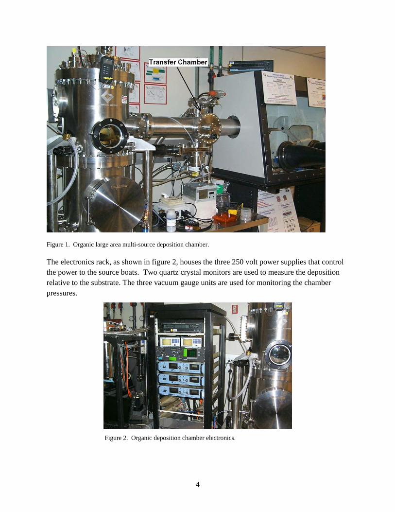
Figure 1. Organic large area multi-source deposition chamber.
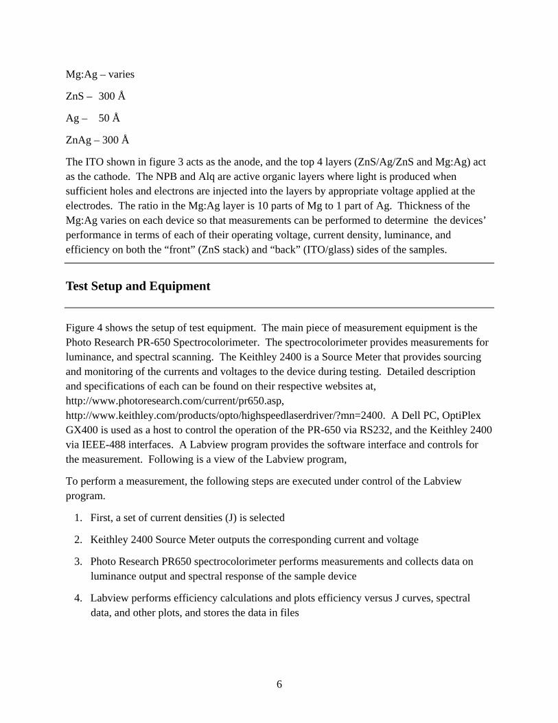
The electronics rack, as shown in figure 2, houses the three 250 volt power supplies that control the power to the source boats. Two quartz crystal monitors are used to measure the deposition relative to the substrate. The three vacuum gauge units are used for monitoring the chamber pressures.
Figure 2. Organic deposition chamber electronics.
4

After the patterned ITO substrates are loaded into the deposition system, the run starts after a base pressure of 1x10⁻⁷ is reached. The OLED structure shown in figure 3 consisted of N,N'-diphenyl-N,N'-(2-naphthyl)-(1,1'-phenyl)-4,4'-diamine (NPB), tris-8-(hydroxyquinoline) aluminum (ALQ), Mg/Ag of varying thicknesses, and lastly the ZnS/Ag/ZnS transparent conducting layer. NPB is an organic thin film that transports holes and ALQ is an organic thin film that transports electrons.
The NPB and ALQ organic layers were grown to thicknesses of 1000 and 600 angstroms respectively using a mask diameter of 0.750”. This organic layer diameter was deposited over the center of the patterned ITO layer. The Mg/Ag conducting layer was deposited on top of the organic layers using a patterned mask to make the connection to separate ITO pads on the substrate. This co-deposited layer used a deposition ratio of 10/1 and thicknesses ranging from 75 to 200 angstroms. Lastly the ZnS/Ag/ZnS transparent conducting layer stack was deposited using the same patterned mask and with thicknesses of 300, 50, 300 angstroms respectively. These thicknesses were used from previous runs for determining optimization.
Once the device was fabricated, a preliminary test was performed in the glove box using a nine volt battery source to ensure device operability. Upon successful device operation, characterization measurements were performed.
Sample Device Structure
Figure 3 shows the structure of the TOLED under study. It consists of the different layers of materials. The devices are fabricated using vacuum thermal evaporation.
ZnS Ag ZnS
Mg:Ag Alq NPB ITO
Glass
Figure 3. TOLED device structure.
The thickness of each layer are shown as follow,
ITO – 400 Å (Angstrom)
NPB – 1000 Å
Alq – 600 Å
5
Mg:Ag – varies
ZnS – 300 Å
Ag – 50 Å
ZnAg – 300 Å
The ITO shown in figure 3 acts as the anode, and the top 4 layers (ZnS/Ag/ZnS and Mg:Ag) act as the cathode. The NPB and Alq are active organic layers where light is produced when sufficient holes and electrons are injected into the layers by appropriate voltage applied at the electrodes. The ratio in the Mg:Ag layer is 10 parts of Mg to 1 part of Ag. Thickness of the Mg:Ag varies on each device so that measurements can be performed to determine the devices’ performance in terms of each of their operating voltage, current density, luminance, and efficiency on both the “front” (ZnS stack) and “back” (ITO/glass) sides of the samples.
Test Setup and Equipment
Figure 4 shows the setup of test equipment. The main piece of measurement equipment is the Photo Research PR-650 Spectrocolorimeter. The spectrocolorimeter provides measurements for luminance, and spectral scanning. The Keithley 2400 is a Source Meter that provides sourcing and monitoring of the currents and voltages to the device during testing. Detailed description and specifications of each can be found on their respective websites at, http://www.photoresearch.com/current/pr650.asp, http://www.keithley.com/products/opto/highspeedlaserdriver/?mn=2400. A Dell PC, OptiPlex GX400 is used as a host to control the operation of the PR-650 via RS232, and the Keithley 2400 via IEEE-488 interfaces. A Labview program provides the software interface and controls for the measurement. Following is a view of the Labview program,
To perform a measurement, the following steps are executed under control of the Labview program.
1. First, a set of current densities (J) is selected
2. Keithley 2400 Source Meter outputs the corresponding current and voltage
3. Photo Research PR650 spectrocolorimeter performs measurements and collects data on luminance output and spectral response of the sample device
4. Labview performs efficiency calculations and plots efficiency versus J curves, spectral data, and other plots, and stores the data in files
6

Figure 4. Picture of the test equipment and setup.
7

In figure 5, the chart in the lower right corner shows the measurement data that are collected and processed. The first column is the selected current density J (step 1 above). Current density here is defined as the current divided by the area of the sample pixel size, in this case 0.1016 cm2. The next column is the voltage needed to produce the J as recorded by the Keithley 2400. The third column is the brightness or luminance in cd/m2, followed by 2 calculated efficiency data columns, and CIE X and Y color coordinates. The 2 plots above the chart are the spectral plot on the left, and the efficiency versus J plot on the right. Usually, the J’s are chosen to show where the peak of the efficiency occurs, and how it rises and decays. Other plots shown are B-V (brightness versus voltage), I-V, and B-I curve on the lower left. Appendix A shows details of key Front Panel and Block Diagram of the Labview program.
Figure 5. A screen shot of Labview program for brightness/efficiency measurement.
Figures 6 and 7 are images of the “front” and “back” view of sample device respectively, showing a lit square pixel.
8

Figure 6. Image of sample device, view from the “back” (ITO/glass) side.
Figure 7. Image of sample device, view from the “front” (ZnS stack) side.
9
Measurements and Results
1. “Standard” Device
A “standard” OLED device (with non-transparent top electrode) with the following structure was first fabricated and measured to establish a baseline for the other measurements.
Figure 8 shows the structure of the “standard” device. It consists of basically the same bottom 3 layers (ITO, NPB, Alq) as those in figure 3, plus a very thick layer of Mg:Ag on top. The thickness of each layer is as follow,
Mg:Ag: 2200 Å;Alq: 600 Å ; NPB: 1000 Å: ITO: 400 Å
Mg:Ag Alq NPB ITO
Glass
Figure 8. Structure of non-transparent “standard” device.
A typical measurement is performed by applying a positive voltage (+) to the anode (ITO electrode) and negative (–) voltage to the cathode Mg:Ag for the Standard device or the Mg:Ag/ZnS/Ag/Zns electrode for the transparent cathode device through Keithley 2400 power source. The voltage and luminance date are measured as a function of the current density (J). The efficiency as a function of current density is calculated and plotted in figure 9 for the typical Standard device configuration.
The measurement data on the “standard” device are shown in appendix B.
10

Efficiency vs. J
2.00
2.10
2.20
2.30
2.40
2.50
2.60
2.70
0.00 10.00 20.00 30.00 40.00 50.00 60.00
J (mA/cm^2)
Effic
ienc
y (C
d/A
)"Standard" Device
Figure 9. Efficiency versus J on “standard” device.
Measurements were made at the glass side as the “standard” device is not transparent. The device shows a typical turn-on voltage of about 5 to 6 volts, and efficiency peak of about 2.65 Cd/A.
2. Sample Devices
Sample devices with Mg:Ag layer thickness of 75 Å, 150 Å, 100 Å, and 200 Å were fabricated. Their measurement data are shown in appendix B.
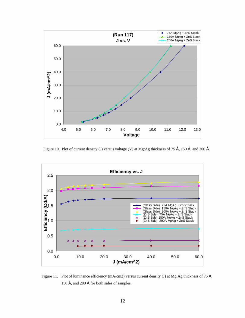
Plots of the current density (J) versus voltage (V), and luminance efficiency versus J are shown in figures 10 and 11 respectively for Mg:Ag thicknesses of 75 Å, 150 Å, and 200 Å.
11
(Run 117)J vs. V
0.0
10.0
20.0
30.0
40.0
50.0
60.0
4.0 5.0 6.0 7.0 8.0 9.0 10.0 11.0 12.0 13.0Voltage
J (m
A/c
m^2
)
75A MgAg + ZnS Stack150A MgAg + ZnS Stack200A MgAg + ZnS Stack
Figure 10. Plot of current density (J) versus voltage (V) at Mg:Ag thickness of 75 Å, 150 Å, and 200 Å.
Efficiency vs. J
0.0
0.5
1.0
1.5
2.0
2.5
0.0 10.0 20.0 30.0 40.0 50.0 60.0J (mA/cm^2)
Effic
ienc
y (C
d/A
)
(Glass Side) 75A MgAg + ZnS Stack (Glass Side) 150A MgAg + ZnS Stack (Glass Side) 200A MgAg + ZnS Stack (ZnS Side) 75A MgAg + ZnS Stack (ZnS Side) 150A MgAg + ZnS Stack (ZnS Side) 200A MgAg + ZnS Stack
Figure 11. Plot of luminance efficiency (mA/cm2) versus current density (J) at Mg:Ag thickness of 75 Å,
150 Å, and 200 Å for both sides of samples.
12
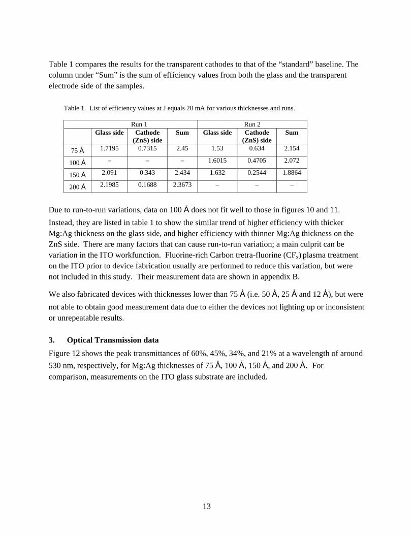
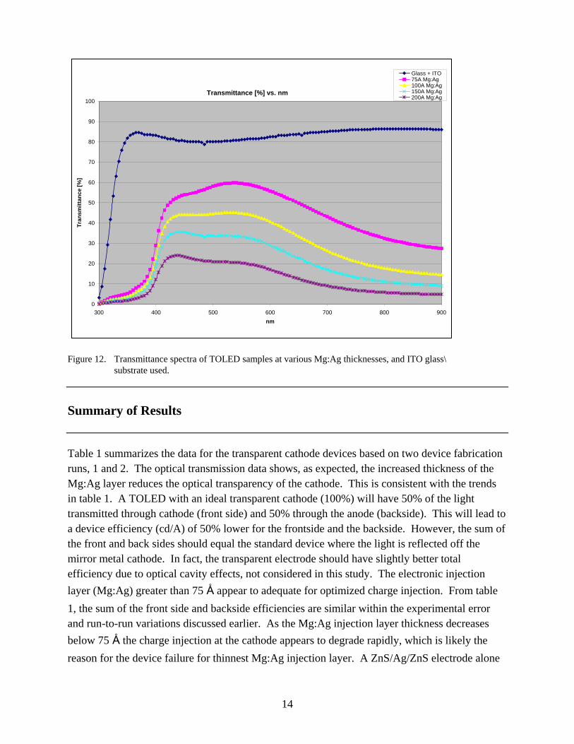
Table 1 compares the results for the transparent cathodes to that of the “standard” baseline. The column under “Sum” is the sum of efficiency values from both the glass and the transparent electrode side of the samples.
Table 1. List of efficiency values at J equals 20 mA for various thicknesses and runs.
Run 1 Run 2 Glass side Cathode
(ZnS) side Sum Glass side Cathode
(ZnS) side Sum
75 Å 1.7195 0.7315 2.45 1.53 0.634 2.154
100 Å – – – 1.6015 0.4705 2.072
150 Å 2.091 0.343 2.434 1.632 0.2544 1.8864
200 Å 2.1985 0.1688 2.3673 – – –
Due to run-to-run variations, data on 100 Å does not fit well to those in figures 10 and 11. Instead, they are listed in table 1 to show the similar trend of higher efficiency with thicker Mg:Ag thickness on the glass side, and higher efficiency with thinner Mg:Ag thickness on the ZnS side. There are many factors that can cause run-to-run variation; a main culprit can be variation in the ITO workfunction. Fluorine-rich Carbon tretra-fluorine (CFx) plasma treatment on the ITO prior to device fabrication usually are performed to reduce this variation, but were not included in this study. Their measurement data are shown in appendix B.
We also fabricated devices with thicknesses lower than 75 Å (i.e. 50 Å, 25 Å and 12 Å), but were not able to obtain good measurement data due to either the devices not lighting up or inconsistent or unrepeatable results.
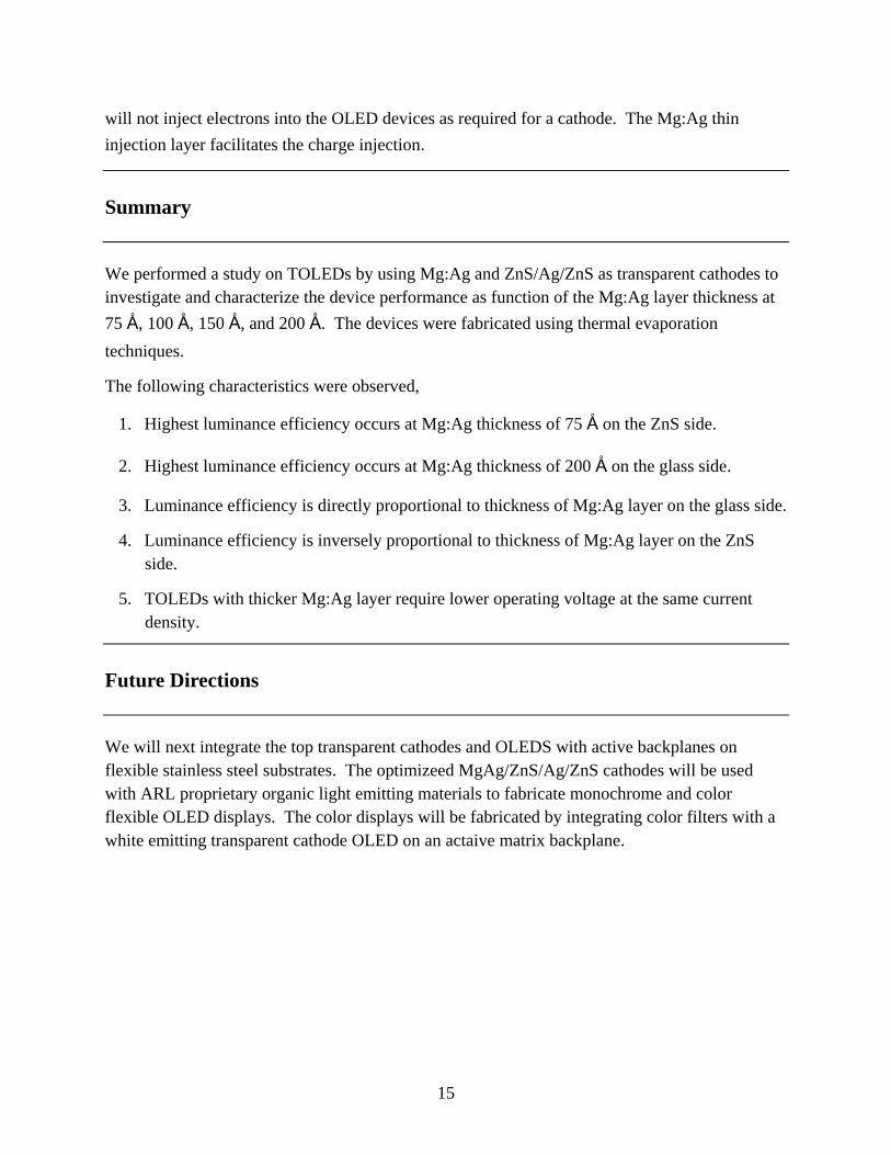
3. Optical Transmission data Figure 12 shows the peak transmittances of 60%, 45%, 34%, and 21% at a wavelength of around 530 nm, respectively, for Mg:Ag thicknesses of 75 Å, 100 Å, 150 Å, and 200 Å. For comparison, measurements on the ITO glass substrate are included.
13
Transmittance [%] vs. nm
0
10
20
30
40
50
60
70
80
90
100
300 400 500 600 700 800 900nm
Tran
smitt
ance
[%]
Glass + ITO75A Mg:Ag100A Mg:Ag150A Mg:Ag200A Mg:Ag
Figure 12. Transmittance spectra of TOLED samples at various Mg:Ag thicknesses, and ITO glass\ substrate used.
Summary of Results
Table 1 summarizes the data for the transparent cathode devices based on two device fabrication runs, 1 and 2. The optical transmission data shows, as expected, the increased thickness of the Mg:Ag layer reduces the optical transparency of the cathode. This is consistent with the trends in table 1. A TOLED with an ideal transparent cathode (100%) will have 50% of the light transmitted through cathode (front side) and 50% through the anode (backside). This will lead to a device efficiency (cd/A) of 50% lower for the frontside and the backside. However, the sum of the front and back sides should equal the standard device where the light is reflected off the mirror metal cathode. In fact, the transparent electrode should have slightly better total efficiency due to optical cavity effects, not considered in this study. The electronic injection layer (Mg:Ag) greater than 75 Å appear to adequate for optimized charge injection. From table 1, the sum of the front side and backside efficiencies are similar within the experimental error and run-to-run variations discussed earlier. As the Mg:Ag injection layer thickness decreases below 75 Å the charge injection at the cathode appears to degrade rapidly, which is likely the reason for the device failure for thinnest Mg:Ag injection layer. A ZnS/Ag/ZnS electrode alone
14
will not inject electrons into the OLED devices as required for a cathode. The Mg:Ag thin injection layer facilitates the charge injection.
Summary
We performed a study on TOLEDs by using Mg:Ag and ZnS/Ag/ZnS as transparent cathodes to investigate and characterize the device performance as function of the Mg:Ag layer thickness at 75 Å, 100 Å, 150 Å, and 200 Å. The devices were fabricated using thermal evaporation techniques.
The following characteristics were observed,
1. Highest luminance efficiency occurs at Mg:Ag thickness of 75 Å on the ZnS side.
2. Highest luminance efficiency occurs at Mg:Ag thickness of 200 Å on the glass side.
3. Luminance efficiency is directly proportional to thickness of Mg:Ag layer on the glass side.
4. Luminance efficiency is inversely proportional to thickness of Mg:Ag layer on the ZnS side.
5. TOLEDs with thicker Mg:Ag layer require lower operating voltage at the same current density.
Future Directions
We will next integrate the top transparent cathodes and OLEDS with active backplanes on flexible stainless steel substrates. The optimizeed MgAg/ZnS/Ag/ZnS cathodes will be used with ARL proprietary organic light emitting materials to fabricate monochrome and color flexible OLED displays. The color displays will be fabricated by integrating color filters with a white emitting transparent cathode OLED on an actaive matrix backplane.
15

References
1. Liu, X.; Cai, X.; Oiao, J.; Mao, J.; Jiang, N. The design of ZnS/Ag/Zns transparent conductive multilayer films. Thin Solid Films 2003, 441, 200–206.
2. Han, S.; Feng, X.; Lu, Z.; Johnson, D.; Wood, R. Transparent-cathode for top-emission organic light-emitting diodes. Applied Physics Letters, 2003, 82 (16), id. 2715.
3. Chen, B.; Sun, X.; Tan, S. C. Transparent oranic light-emitting devices with LiF/Mg:Ag cathode. Optics Express February 2005, 13 (3).
16

Appendix A. LabView Program
Front Panel
17

Block Diagram
18
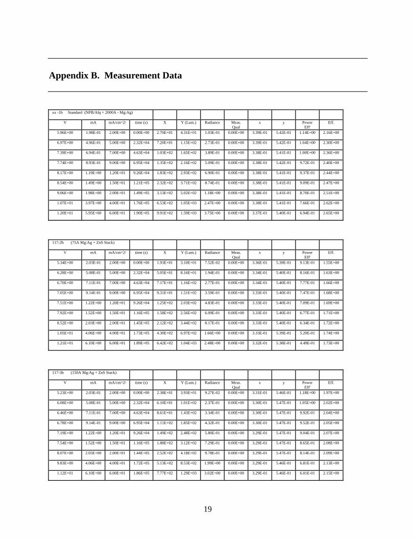
Appendix B. Measurement Data
xx -1b Standard (NPB/Alq + 2000A - Mg:Ag)
V mA mA/cm^2/ time (s) X Y (Lum.) Radiance Meas. Qual
x y Power Eff'
Eff. 5.96E+00 1.98E-01 2.00E+00 0.00E+00 2.70E+01 4.31E+01 1.03E-01 0.00E+00 3.39E-01 5.42E-01 1.14E+00 2.16E+00 6.97E+00 4.96E-01 5.00E+00 2.32E+04 7.20E+01 1.15E+02 2.73E-01 0.00E+00 3.39E-01 5.42E-01 1.04E+00 2.30E+00 7.39E+00 6.94E-01 7.00E+00 4.63E+04 1.03E+02 1.65E+02 3.89E-01 0.00E+00 3.38E-01 5.41E-01 1.00E+00 2.36E+00 7.74E+00 8.93E-01 9.00E+00 6.95E+04 1.35E+02 2.16E+02 5.09E-01 0.00E+00 3.38E-01 5.42E-01 9.72E-01 2.40E+00 8.17E+00 1.19E+00 1.20E+01 9.26E+04 1.83E+02 2.93E+02 6.90E-01 0.00E+00 3.38E-01 5.41E-01 9.37E-01 2.44E+00 8.54E+00 1.49E+00 1.50E+01 1.21E+05 2.32E+02 3.71E+02 8.74E-01 0.00E+00 3.38E-01 5.41E-01 9.09E-01 2.47E+00 9.06E+00 1.98E+00 2.00E+01 1.49E+05 3.13E+02 5.02E+02 1.18E+00 0.00E+00 3.38E-01 5.41E-01 8.70E-01 2.51E+00 1.07E+01 3.97E+00 4.00E+01 1.76E+05 6.53E+02 1.05E+03 2.47E+00 0.00E+00 3.38E-01 5.41E-01 7.66E-01 2.62E+00 1.20E+01 5.95E+00 6.00E+01 1.90E+05 9.91E+02 1.59E+03 3.75E+00 0.00E+00 3.37E-01 5.40E-01 6.94E-01 2.65E+00
117-2b (75A Mg:Ag + ZnS Stack) V mA mA/cm^2/ time (s) X Y (Lum.) Radiance Meas.
Qual x y Power
Eff' Eff.
5.34E+00 2.03E-01 2.00E+00 0.00E+00 1.93E+01 3.10E+01 7.52E-02 0.00E+00 3.36E-01 5.39E-01 9.13E-01 1.55E+00 6.28E+00 5.08E-01 5.00E+00 2.32E+04 5.05E+01 8.16E+01 1.94E-01 0.00E+00 3.34E-01 5.40E-01 8.16E-01 1.63E+00 6.70E+00 7.11E-01 7.00E+00 4.63E+04 7.17E+01 1.16E+02 2.77E-01 0.00E+00 3.34E-01 5.40E-01 7.77E-01 1.66E+00 7.05E+00 9.14E-01 9.00E+00 6.95E+04 9.31E+01 1.51E+02 3.59E-01 0.00E+00 3.33E-01 5.40E-01 7.47E-01 1.68E+00 7.51E+00 1.22E+00 1.20E+01 9.26E+04 1.25E+02 2.03E+02 4.83E-01 0.00E+00 3.33E-01 5.40E-01 7.09E-01 1.69E+00 7.92E+00 1.52E+00 1.50E+01 1.16E+05 1.58E+02 2.56E+02 6.09E-01 0.00E+00 3.33E-01 5.40E-01 6.77E-01 1.71E+00 8.52E+00 2.03E+00 2.00E+01 1.45E+05 2.12E+02 3.44E+02 8.17E-01 0.00E+00 3.33E-01 5.40E-01 6.34E-01 1.72E+00 1.05E+01 4.06E+00 4.00E+01 1.73E+05 4.30E+02 6.97E+02 1.66E+00 0.00E+00 3.33E-01 5.39E-01 5.20E-01 1.74E+00 1.21E+01 6.10E+00 6.00E+01 1.89E+05 6.42E+02 1.04E+03 2.48E+00 0.00E+00 3.32E-01 5.38E-01 4.49E-01 1.73E+00
117-3b (150A Mg:Ag + ZnS Stack) V mA mA/cm^2/ time (s) X Y (Lum.) Radiance Meas.
Qual x y Power
Eff' Eff.
5.23E+00 2.03E-01 2.00E+00 0.00E+00 2.38E+01 3.93E+01 9.27E-02 0.00E+00 3.31E-01 5.46E-01 1.18E+00 1.97E+00 6.08E+00 5.08E-01 5.00E+00 2.32E+04 6.10E+01 1.01E+02 2.37E-01 0.00E+00 3.30E-01 5.47E-01 1.05E+00 2.02E+00 6.46E+00 7.11E-01 7.00E+00 4.63E+04 8.61E+01 1.43E+02 3.34E-01 0.00E+00 3.30E-01 5.47E-01 9.92E-01 2.04E+00 6.78E+00 9.14E-01 9.00E+00 6.95E+04 1.11E+02 1.85E+02 4.32E-01 0.00E+00 3.30E-01 5.47E-01 9.52E-01 2.05E+00 7.19E+00 1.22E+00 1.20E+01 9.26E+04 1.49E+02 2.48E+02 5.80E-01 0.00E+00 3.29E-01 5.47E-01 9.04E-01 2.07E+00 7.54E+00 1.52E+00 1.50E+01 1.16E+05 1.88E+02 3.12E+02 7.29E-01 0.00E+00 3.29E-01 5.47E-01 8.65E-01 2.08E+00 8.07E+00 2.03E+00 2.00E+01 1.44E+05 2.52E+02 4.18E+02 9.78E-01 0.00E+00 3.29E-01 5.47E-01 8.14E-01 2.09E+00 9.83E+00 4.06E+00 4.00E+01 1.72E+05 5.13E+02 8.53E+02 1.99E+00 0.00E+00 3.29E-01 5.46E-01 6.81E-01 2.13E+00 1.12E+01 6.10E+00 6.00E+01 1.86E+05 7.77E+02 1.29E+03 3.02E+00 0.00E+00 3.29E-01 5.46E-01 6.01E-01 2.15E+00
19

117-4a (200A Mg:Ag + ZnS Stack) V mA mA/cm^2/ time (s) X Y (Lum.) Radiance Meas.
Qual x y Power
Eff' Eff.
5.27E+00 2.03E-01 2.00E+00 0.00E+00 2.44E+01 4.12E+01 9.69E-02 0.00E+00 3.25E-01 5.48E-01 1.23E+00 2.06E+00 6.11E+00 5.08E-01 5.00E+00 2.32E+04 6.24E+01 1.06E+02 2.47E-01 0.00E+00 3.25E-01 5.50E-01 1.09E+00 2.12E+00 6.48E+00 7.11E-01 7.00E+00 4.63E+04 8.82E+01 1.50E+02 3.48E-01 0.00E+00 3.24E-01 5.50E-01 1.04E+00 2.14E+00 6.80E+00 9.14E-01 9.00E+00 6.94E+04 1.14E+02 1.94E+02 4.50E-01 0.00E+00 3.24E-01 5.50E-01 9.94E-01 2.15E+00 7.20E+00 1.22E+00 1.20E+01 9.26E+04 1.53E+02 2.60E+02 6.05E-01 0.00E+00 3.24E-01 5.50E-01 9.46E-01 2.17E+00 7.55E+00 1.52E+00 1.50E+01 1.21E+05 1.93E+02 3.27E+02 7.61E-01 0.00E+00 3.24E-01 5.50E-01 9.07E-01 2.18E+00 8.08E+00 2.03E+00 2.00E+01 1.50E+05 2.59E+02 4.40E+02 1.02E+00 0.00E+00 3.24E-01 5.50E-01 8.55E-01 2.20E+00 9.82E+00 4.06E+00 4.00E+01 1.77E+05 5.29E+02 8.98E+02 2.09E+00 0.00E+00 3.24E-01 5.49E-01 7.18E-01 2.25E+00 1.12E+01 6.10E+00 6.00E+01 1.91E+05 8.03E+02 1.36E+03 3.18E+00 0.00E+00 3.23E-01 5.48E-01 6.36E-01 2.27E+00
117-2b (75A Mg:Ag + ZnS Stack) ** (ZnS
side)
V mA mA/cm^2/ time (s) X Y (Lum.) Radiance Meas. Qual
x y Power Eff'
Eff. 5.32E+00 2.03E-01 2.00E+00 0.00E+00 7.76E+00 1.35E+01 3.28E-02 0.00E+00 3.15E-01 5.46E-01 3.98E-01 6.73E-01 6.26E+00 5.08E-01 5.00E+00 2.32E+04 1.97E+01 3.47E+01 8.17E-02 0.00E+00 3.13E-01 5.50E-01 3.49E-01 6.95E-01 6.70E+00 7.11E-01 7.00E+00 4.63E+04 2.79E+01 4.93E+01 1.15E-01 0.00E+00 3.12E-01 5.51E-01 3.30E-01 7.04E-01 7.09E+00 9.14E-01 9.00E+00 6.95E+04 3.62E+01 6.40E+01 1.49E-01 0.00E+00 3.12E-01 5.51E-01 3.15E-01 7.11E-01 7.60E+00 1.22E+00 1.20E+01 9.26E+04 4.87E+01 8.62E+01 2.00E-01 0.00E+00 3.12E-01 5.52E-01 2.97E-01 7.19E-01 8.08E+00 1.52E+00 1.50E+01 1.16E+05 6.14E+01 1.09E+02 2.52E-01 0.00E+00 3.12E-01 5.52E-01 2.82E-01 7.25E-01 8.83E+00 2.03E+00 2.00E+01 1.39E+05 8.26E+01 1.46E+02 3.38E-01 0.00E+00 3.12E-01 5.52E-01 2.60E-01 7.32E-01 1.14E+01 4.06E+00 4.00E+01 1.62E+05 1.68E+02 2.98E+02 6.90E-01 0.00E+00 3.11E-01 5.51E-01 2.05E-01 7.45E-01 1.42E+01 6.10E+00 6.00E+01 1.90E+05 2.50E+02 4.42E+02 1.03E+00 0.00E+00 3.11E-01 5.50E-01 1.63E-01 7.37E-01
117-3a (150A Mg:Ag + ZnS Stack) ** (ZnS
side)
V mA mA/cm^2/ time (s) X Y (Lum.) Radiance Meas. Qual
x y Power Eff'
Eff. 5.22E+00 2.03E-01 2.00E+00 0.00E+00 3.61E+00 6.64E+00 1.75E-02 1.80E+01 2.97E-01 5.47E-01 2.00E-01 3.32E-01 6.05E+00 5.08E-01 5.00E+00 2.32E+04 8.96E+00 1.68E+01 4.13E-02 0.00E+00 2.94E-01 5.52E-01 1.75E-01 3.36E-01 6.42E+00 7.11E-01 7.00E+00 4.63E+04 1.25E+01 2.35E+01 5.63E-02 0.00E+00 2.94E-01 5.53E-01 1.65E-01 3.36E-01 6.73E+00 9.14E-01 9.00E+00 6.96E+04 1.61E+01 3.04E+01 7.23E-02 0.00E+00 2.93E-01 5.53E-01 1.58E-01 3.38E-01 7.14E+00 1.22E+00 1.20E+01 9.28E+04 2.15E+01 4.08E+01 9.62E-02 0.00E+00 2.93E-01 5.54E-01 1.49E-01 3.40E-01 7.50E+00 1.52E+00 1.50E+01 1.16E+05 2.69E+01 5.11E+01 1.20E-01 0.00E+00 2.92E-01 5.55E-01 1.43E-01 3.41E-01 8.03E+00 2.03E+00 2.00E+01 1.39E+05 3.61E+01 6.86E+01 1.61E-01 0.00E+00 2.92E-01 5.55E-01 1.34E-01 3.43E-01 9.81E+00 4.06E+00 4.00E+01 1.63E+05 7.36E+01 1.40E+02 3.26E-01 0.00E+00 2.92E-01 5.54E-01 1.12E-01 3.49E-01 1.12E+01 6.10E+00 6.00E+01 1.86E+05 1.11E+02 2.10E+02 4.90E-01 0.00E+00 2.91E-01 5.53E-01 9.81E-02 3.50E-01
117-4a (200A Mg:Ag + ZnS Stack)
20

** (ZnS side)
V mA mA/cm^2/ time (s) X Y (Lum.) Radiance Meas.
Qual x y Power
Eff' Eff.
5.26E+00 2.03E-01 2.00E+00 0.00E+00 5.05E+01 9.95E+01 2.36E-01 1.00E+01 2.80E-01 5.51E-01 2.98E+00 4.98E+00 6.12E+00 5.08E-01 5.00E+00 2.27E+04 4.20E+00 8.18E+00 2.15E-02 1.80E+01 2.83E-01 5.51E-01 8.40E-02 1.64E-01 6.51E+00 7.11E-01 7.00E+00 4.59E+04 5.92E+00 1.15E+01 2.89E-02 1.80E+01 2.81E-01 5.49E-01 7.96E-02 1.65E-01 6.84E+00 9.14E-01 9.00E+00 6.90E+04 7.58E+00 1.49E+01 3.70E-02 0.00E+00 2.81E-01 5.51E-01 7.59E-02 1.65E-01 7.26E+00 1.22E+00 1.20E+01 9.22E+04 1.01E+01 1.99E+01 4.84E-02 0.00E+00 2.81E-01 5.52E-01 7.19E-02 1.66E-01 7.63E+00 1.52E+00 1.50E+01 1.15E+05 1.28E+01 2.51E+01 6.11E-02 0.00E+00 2.81E-01 5.52E-01 6.89E-02 1.67E-01 8.18E+00 2.03E+00 2.00E+01 1.38E+05 1.71E+01 3.38E+01 8.07E-02 0.00E+00 2.81E-01 5.53E-01 6.48E-02 1.69E-01 1.00E+01 4.06E+00 4.00E+01 1.62E+05 3.49E+01 6.88E+01 1.63E-01 0.00E+00 2.81E-01 5.53E-01 5.40E-02 1.72E-01 1.15E+01 6.10E+00 6.00E+01 1.85E+05 5.26E+01 1.04E+02 2.45E-01 0.00E+00 2.80E-01 5.52E-01 4.73E-02 1.73E-01
111-1a (100A MgAg + ZnS Stack) V mA mA/cm^2/ time (s) X Y (Lum.) Radiance Meas.
Qual x y Power
Eff' Eff.
4.84E+00 2.03E-01 2.00E+00 0.00E+00 1.69E+01 2.78E+01 6.67E-02 0.00E+00 3.30E-01 5.42E-01 9.04E-01 1.39E+00 5.63E+00 5.08E-01 5.00E+00 2.32E+04 4.49E+01 7.42E+01 1.76E-01 0.00E+00 3.29E-01 5.44E-01 8.28E-01 1.48E+00 6.00E+00 7.11E-01 7.00E+00 4.63E+04 6.41E+01 1.06E+02 2.51E-01 0.00E+00 3.28E-01 5.43E-01 7.93E-01 1.51E+00 6.31E+00 9.14E-01 9.00E+00 6.95E+04 8.36E+01 1.38E+02 3.27E-01 0.00E+00 3.28E-01 5.43E-01 7.66E-01 1.54E+00 6.71E+00 1.22E+00 1.20E+01 9.26E+04 1.13E+02 1.87E+02 4.42E-01 0.00E+00 3.28E-01 5.44E-01 7.31E-01 1.56E+00 7.07E+00 1.52E+00 1.50E+01 1.16E+05 1.43E+02 2.37E+02 5.58E-01 0.00E+00 3.28E-01 5.44E-01 7.02E-01 1.58E+00 7.60E+00 2.03E+00 2.00E+01 1.39E+05 1.93E+02 3.20E+02 7.55E-01 0.00E+00 3.28E-01 5.43E-01 6.62E-01 1.60E+00 9.39E+00 4.06E+00 4.00E+01 1.67E+05 4.01E+02 6.65E+02 1.57E+00 0.00E+00 3.28E-01 5.43E-01 5.56E-01 1.66E+00 1.08E+01 6.10E+00 6.00E+01 1.83E+05 6.09E+02 1.01E+03 2.38E+00 0.00E+00 3.27E-01 5.42E-01 4.88E-01 1.68E+00
111-3a (150A MgAg + ZnS Stack) V mA mA/cm^2/ time (s) X Y (Lum.) Radiance Meas.
Qual x y Power
Eff' Eff.
4.79E+00 2.03E-01 2.00E+00 0.00E+00 1.69E+01 2.85E+01 6.84E-02 0.00E+00 3.22E-01 5.44E-01 9.34E-01 1.43E+00 5.55E+00 5.08E-01 5.00E+00 2.32E+04 4.49E+01 7.59E+01 1.80E-01 0.00E+00 3.22E-01 5.45E-01 8.60E-01 1.52E+00 5.89E+00 7.11E-01 7.00E+00 4.63E+04 6.41E+01 1.09E+02 2.56E-01 0.00E+00 3.22E-01 5.45E-01 8.28E-01 1.55E+00 6.17E+00 9.14E-01 9.00E+00 6.94E+04 8.34E+01 1.41E+02 3.34E-01 0.00E+00 3.21E-01 5.45E-01 8.00E-01 1.57E+00 6.55E+00 1.22E+00 1.20E+01 9.26E+04 1.13E+02 1.91E+02 4.52E-01 0.00E+00 3.21E-01 5.45E-01 7.66E-01 1.60E+00 6.87E+00 1.52E+00 1.50E+01 1.16E+05 1.43E+02 2.42E+02 5.71E-01 0.00E+00 3.21E-01 5.45E-01 7.37E-01 1.61E+00 7.36E+00 2.03E+00 2.00E+01 1.39E+05 1.92E+02 3.26E+02 7.70E-01 0.00E+00 3.21E-01 5.45E-01 6.97E-01 1.63E+00 8.98E+00 4.06E+00 4.00E+01 1.67E+05 3.97E+02 6.74E+02 1.59E+00 0.00E+00 3.21E-01 5.44E-01 5.89E-01 1.68E+00 1.03E+01 6.10E+00 6.00E+01 1.82E+05 6.01E+02 1.02E+03 2.41E+00 0.00E+00 3.20E-01 5.43E-01 5.20E-01 1.70E+00
111-1a (100A MgAg + ZnS Stack) **Back Side
V mA mA/cm^2/ time (s) X Y (Lum.) Radiance Meas. Qual
x y Power Eff'
Eff. 4.83E+00 2.03E-01 2.00E+00 0.00E+00 4.78E+00 8.48E+00 2.18E-02 1.80E+01 3.07E-01 5.46E-01 2.76E-01 4.24E-01
21
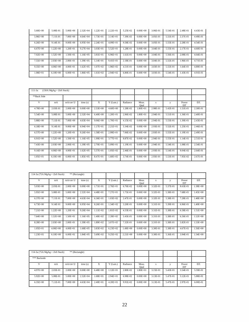
5.60E+00 5.08E-01 5.00E+00 2.32E+04 1.22E+01 2.22E+01 5.25E-02 0.00E+00 3.06E-01 5.54E-01 2.48E-01 4.43E-01 5.96E+00 7.11E-01 7.00E+00 4.64E+04 1.73E+01 3.14E+01 7.39E-02 0.00E+00 3.05E-01 5.55E-01 2.37E-01 4.49E-01 6.26E+00 9.14E-01 9.00E+00 6.95E+04 2.24E+01 4.09E+01 9.58E-02 0.00E+00 3.05E-01 5.55E-01 2.28E-01 4.54E-01 6.67E+00 1.22E+00 1.20E+01 9.27E+04 3.03E+01 5.52E+01 1.28E-01 0.00E+00 3.04E-01 5.55E-01 2.17E-01 4.60E-01 7.02E+00 1.52E+00 1.50E+01 1.16E+05 3.81E+01 6.96E+01 1.61E-01 0.00E+00 3.04E-01 5.56E-01 2.08E-01 4.64E-01 7.55E+00 2.03E+00 2.00E+01 1.39E+05 5.14E+01 9.41E+01 2.18E-01 0.00E+00 3.04E-01 5.55E-01 1.96E-01 4.71E-01 9.35E+00 4.06E+00 4.00E+01 1.62E+05 1.07E+02 1.96E+02 4.51E-01 0.00E+00 3.03E-01 5.55E-01 1.64E-01 4.89E-01 1.08E+01 6.10E+00 6.00E+01 1.86E+05 1.61E+02 2.94E+02 6.80E-01 0.00E+00 3.03E-01 5.54E-01 1.43E-01 4.91E-01
111-3a (150A MgAg + ZnS Stack) **Back Side
V mA mA/cm^2/ time (s) X Y (Lum.) Radiance Meas. Qual
x y Power Eff'
Eff. 4.78E+00 2.03E-01 2.00E+00 0.00E+00 2.53E+00 4.60E+00 1.28E-02 1.80E+01 2.98E-01 5.42E-01 1.51E-01 2.30E-01 5.54E+00 5.08E-01 5.00E+00 2.32E+04 6.40E+00 1.20E+01 2.96E-02 1.80E+01 2.94E-01 5.51E-01 1.36E-01 2.40E-01 5.88E+00 7.11E-01 7.00E+00 4.63E+04 9.06E+00 1.70E+01 4.15E-02 0.00E+00 2.94E-01 5.53E-01 1.30E-01 2.43E-01 6.18E+00 9.14E-01 9.00E+00 6.94E+04 1.17E+01 2.21E+01 5.34E-02 0.00E+00 2.93E-01 5.52E-01 1.25E-01 2.46E-01 6.57E+00 1.22E+00 1.20E+01 9.26E+04 1.58E+01 2.99E+01 7.06E-02 0.00E+00 2.93E-01 5.55E-01 1.19E-01 2.49E-01 6.91E+00 1.52E+00 1.50E+01 1.16E+05 1.99E+01 3.77E+01 8.87E-02 0.00E+00 2.94E-01 5.55E-01 1.14E-01 2.51E-01 7.43E+00 2.03E+00 2.00E+01 1.39E+05 2.70E+01 5.09E+01 1.19E-01 0.00E+00 2.94E-01 5.54E-01 1.08E-01 2.54E-01 9.16E+00 4.06E+00 4.00E+01 1.62E+05 5.57E+01 1.05E+02 2.46E-01 0.00E+00 2.93E-01 5.54E-01 9.04E-02 2.64E-01 1.05E+01 6.10E+00 6.00E+01 1.85E+05 8.47E+01 1.60E+02 3.74E-01 0.00E+00 2.93E-01 5.53E-01 7.95E-02 2.67E-01
114-3a (75A MgAg + ZnS Stack) ** (Rectangle) V mA mA/cm^2/ time (s) X Y (Lum.) Radiance Meas.
Qual x y Power
Eff' Eff.
5.03E+00 2.03E-01 2.00E+00 0.00E+00 1.71E+01 2.76E+01 6.76E-02 0.00E+00 3.32E-01 5.37E-01 8.63E-01 1.38E+00 5.95E+00 5.08E-01 5.00E+00 2.32E+04 4.48E+01 7.27E+01 1.75E-01 0.00E+00 3.32E-01 5.38E-01 7.68E-01 1.45E+00 6.37E+00 7.11E-01 7.00E+00 4.63E+04 6.36E+01 1.03E+02 2.47E-01 0.00E+00 3.32E-01 5.38E-01 7.28E-01 1.48E+00 6.73E+00 9.14E-01 9.00E+00 6.95E+04 8.26E+01 1.34E+02 3.20E-01 0.00E+00 3.31E-01 5.39E-01 6.96E-01 1.49E+00 7.21E+00 1.22E+00 1.20E+01 9.26E+04 1.11E+02 1.81E+02 4.33E-01 0.00E+00 3.31E-01 5.38E-01 6.58E-01 1.51E+00 7.64E+00 1.52E+00 1.50E+01 1.16E+05 1.40E+02 2.28E+02 5.45E-01 0.00E+00 3.31E-01 5.38E-01 6.26E-01 1.52E+00 8.28E+00 2.03E+00 2.00E+01 1.39E+05 1.89E+02 3.07E+02 7.32E-01 0.00E+00 3.31E-01 5.38E-01 5.82E-01 1.53E+00 1.05E+01 4.06E+00 4.00E+01 1.68E+05 3.83E+02 6.23E+02 1.49E+00 0.00E+00 3.30E-01 5.38E-01 4.67E-01 1.56E+00 1.23E+01 6.10E+00 6.00E+01 1.84E+05 5.69E+02 9.25E+02 2.21E+00 0.00E+00 3.30E-01 5.36E-01 3.94E-01 1.54E+00
114-3a (75A MgAg + ZnS Stack) ** (Rectangle) *** Backside
V mA mA/cm^2/ time (s) X Y (Lum.) Radiance Meas. Qual
x y Power Eff'
Eff. 4.97E+00 2.03E-01 2.00E+00 0.00E+00 6.48E+00 1.12E+01 2.80E-02 1.80E+01 3.15E-01 5.43E-01 3.54E-01 5.59E-01 5.92E+00 5.08E-01 5.00E+00 2.32E+04 1.68E+01 2.94E+01 6.98E-02 0.00E+00 3.13E-01 5.47E-01 3.12E-01 5.88E-01 6.35E+00 7.11E-01 7.00E+00 4.63E+04 2.40E+01 4.20E+01 9.91E-02 0.00E+00 3.13E-01 5.47E-01 2.97E-01 6.00E-01
22

6.71E+00 9.14E-01 9.00E+00 6.95E+04 3.12E+01 5.47E+01 1.29E-01 0.00E+00 3.12E-01 5.47E-01 2.85E-01 6.08E-01 7.19E+00 1.22E+00 1.20E+01 9.27E+04 4.22E+01 7.41E+01 1.74E-01 0.00E+00 3.12E-01 5.48E-01 2.70E-01 6.18E-01 7.62E+00 1.52E+00 1.50E+01 1.16E+05 5.33E+01 9.37E+01 2.19E-01 0.00E+00 3.12E-01 5.48E-01 2.58E-01 6.25E-01 8.26E+00 2.03E+00 2.00E+01 1.39E+05 7.22E+01 1.27E+02 2.96E-01 0.00E+00 3.12E-01 5.48E-01 2.41E-01 6.34E-01 1.04E+01 4.06E+00 4.00E+01 1.62E+05 1.49E+02 2.62E+02 6.12E-01 0.00E+00 3.11E-01 5.47E-01 1.97E-01 6.56E-01 1.23E+01 6.10E+00 6.00E+01 1.91E+05 2.25E+02 3.95E+02 9.25E-01 0.00E+00 3.11E-01 5.46E-01 1.69E-01 6.58E-01
23

24
INTENTIONALLY LEFT BLANK
Distribution List
ADMNSTR DEFNS TECHL INFO CTR ATTN DTIC-OCP (ELECTRONIC COPY) 8725 JOHN J KINGMAN RD STE 0944 FT BELVOIR VA 22060-6218 DARPA ATTN IXO S WELBY 3701 N FAIRFAX DR ARLINGTON VA 22203-1714 OFC OF THE SECY OF DEFNS ATTN ODDRE (R&AT) THE PENTAGON WASHINGTON DC 20301-3080 US ARMY RSRCH DEV AND ENGRG CMND ARMAMENT RSRCH DEV AND ENGRG CTR ARMAMENT ENGRG AND TECHNLGY CTR ATTN AMSRD-AAR-AEF-T J MATTS BLDG 305 ABERDEEN PROVING GROUND MD 21005-5001 US ARMY TRADOC BATTLE LAB INTEGRATION & TECHL DIRCTRT ATTN ATCD-B 10 WHISTLER LANE FT MONROE VA 23651-5850 SMC/GPA 2420 VELA WAY STE 1866 EL SEGUNDO CA 90245-4659 US ARMY INFO SYS ENGRG CMND ATTN AMSEL-IE-TD F JENIA FT HUACHUCA AZ 85613-5300
COMMANDER US ARMY RDECOM ATTN AMSRD-AMR W C MCCORKLE 5400 FOWLER RD REDSTONE ARSENAL AL 35898-5000 US ARMY RSRCH LAB ATTN AMSRD-ARL-CI-OK-TP TECHL LIB T LANDFRIED BLDG 4600 ABERDEEN PROVING GROUND MD 21005-5066 US GOVERNMENT PRINT OFF DEPOSITORY RECEIVING SECTION ATTN MAIL STOP IDAD J TATE 732 NORTH CAPITOL ST., NW WASHINGTON DC 20402 DIRECTOR US ARMY RSRCH LAB ATTN AMSRD-ARL-RO-EV W D BACH PO BOX 12211 RESEARCH TRIANGLE PARK NC 27709 US ARMY RSRCH LAB ATTN AMSRD-ARL-CI-OK-T TECHL PUB (2 COPIES) ATTN AMSRD-ARL-CI-OK-TL TECHL LIB ATTN AMSRD-ARL-D J M MILLER ATTN AMSRD-ARL-SE-EE D CHIU (10 COPIES) ATTN AMSRD-ARL-SE-EE D MORTON ATTN AMSRD-ARL-SE-EE E FORSYTH ATTN AMSRD-ARL-SE-EE J SHI ATTN AMSRD-ARL-SE-EE K ALIBERTI ATTN AMSRD-ARL-SE-EE S BLOMQUIST ATTN IMNE-ALC-IMS MAIL & RECORDS MGMT ADELPHI MD 20783-1197
25

INTENTIONALLY LEFT BLANK
26