characteristics of tunneling p-n junctions - nasa · characteristics of tunneling p-n ... microwave...
TRANSCRIPT

c I
CHARACTERISTICS OF TUNNELING P-N JUNCTIONS
by John B. Hopkins
Electronics Research Center Cam bridge, Mass,
N A T I O N A L AERONAUTICS A N D SPACE A D M I N I S T R A T I O N W A S H I N G T O N , D. C. 0 M A R C H 1 9 6 8
https://ntrs.nasa.gov/search.jsp?R=19680009593 2018-07-01T04:46:20+00:00Z

TECH LIBRARY KAFB. NM
CHARACTERISTICS
OF
TUNNELING P-N JUNCTIONS
By John B. Hopkins
Electronics Research Center Cambridge, Mass.
c
NATIONAL AERONAUTICS AND SPACE ADMINISTRATION
For so le by the Clearinghouse for Federal Scientific and Technical Information Springfield, Virginia 22151 - CFSTI price $3.00

CHARACTERISTICS O F TUNNELING P - N JUNCTIONS
By John B. Hopkins Electronics Research Center
SUMMARY
c Procedures have been developed for the calculation of current-voltage
character is t ics of tunneling p-n junctions in semiconductors, given mater ia l
acquired in similar efforts has been attained. used, numerical differentiation permits calculation of parameters relevant to microwave mixing and detecting applications for tunnel and backward diodes in any elemental o r compound semiconductor. Typical resul ts a r e indicated.
1 constants and impurity-doping parameters . Accuracy higher than that When a digital computer i s
I I
I INTRODUCTION
This report concerns research done in the fabrication and characterization They a r e in- of backward diodes made f rom a variety of III-V semiconductors.
tended for use in microwave mixing and detecting applications. effort requires estimation of tunnel diode characterist ics in a number of mate- r ia ls and for varying impurity concentrations. F o r example, it i s useful to be able to estimate figures of mer i t which involve the f i r s t and second derivatives of the i -v curve, and these can be meaningful only with a fairly accurate know- ledge of i(v). parameters of a p-n junction tunnel diode i s a problem not amenable to an ana- lytical approach.
The research
Determination of the theoretical i -v characterist ics and other
I A number of authors ( r e f s . 1 , 2 , 3 and 4) have used greatly simplified models to obtain various numerical o r analytical resul ts , but--in addition to their very approximate nature- -these solutions a r e limited in the information provided. This report describes resul ts obtainable by use of an analysis sig- nificantly more detailed than that conventionally used. These calculations , facilitated by use of a digital computer, can be made to a significantly higher degree of accuracy than those previously reported.
c It should be noted, however, that the calculations, though detailed, a r e
ultimately based on the conventional physical model, and a r e therefore sub- ject to e r r o r s resulting f rom the inadequacies of that representation. weaknesses will be indicated at relevant points in the detailed description of the model and the calculations.
I: These

THE PHYSICAL MODEL
The model used i s a conventional p-n junction. Perfect crystal s t ructure i s assumed, with an impurity concentration which changes abruptly f rom Nd, at energy -Ed (n-region), to Nay at energy Ea (p-region). It should be noted that no rea l junction can be t ruly abrupt, and this assumption may well lead to inaccuracies when applied to tunneling junctions. F o r these, the "abruptness" condition (that the depletion layer be much wider than the region of changing impurity concentration) i s seriously violated. Nor a r e defects of any type con- sidered, so that this program does not show excess current. While this is a definite limitation for application to tunnel diodes (the peak- to-valley cur ren t ratio cannot be estimated, for example), it i s forced by the theoretical com- plexity of the problem.
Y
L
Further , it i s of l e s s relevance to backward diode studies, where opera- The band tion i s generally a t very low bias, and excess current i s small.
structure i s taken to be particularly simple- -parabolic, and isotropic i n x . Also, only direct tunneling transitions a r e considered. ous restriction, since both germanium and silicon a r e indirect-gap mater ia ls However, the principal e r r o r will be only in current densities, so much useful information can be obtained for these mater ia ls a s well. (Most 111-V semi- conductors of current interest a r e essentially direct-gap and accurate es t i - mates can be obtained for them. )
This could be a ser i -
Tunneling current i s a very sensitive function of tunneling distance, and considerable c a r e i s taken in determining this parameter . The various mate- rial constants a r e specified for the temperature assumed, and a r e taken to be independent of applied voltage and F e r m i levels, and as constant throughout the material . However, variation of the diffusion constant with the position of the F e r m i level is included.
Discussion of tunnel diodes necessar i ly requires consideration of degen- e ra te and near-degenerate conditions , and difficulties do ar ise--for example, in determination of the F e r m i levels. Fortunately, some uncertainty in this does not seriously affect resul ts in the region of principal interest . Fur ther , an approximation has been developed which seems sufficiently accurate.
? The required data for the mater ia l includes band gap, dielectric constant,
lattice constant, and hole and electron mobilities, effective masses , and re- combination t imes. using the Einstein relation (D = kTp/q), corrected for degeneracy. sion lengths a r e determined f rom the diffusion constants and recombination t imes
The diffusion constants a r e calculated f rom the mobilities , The diffu-
2

In addition, the impurity doping parameters a r e read in. concentrations and energy levels. impurity scattering for increasing doping density i s incorporated by use of the Dingle- Brooks expression for impurity mobility.
These include both Variation of mobility caused by increased
As the program is intended to provide information about phenomena asso- ciated with low voltages only, no breakdown mechanisms have been included in the diode model.
3

DETAILS OF THE CALCULATIONS
The first step in determining the electrical character is t ics of a semi-
The basic equation used i s conductor is calculation of the position of the F e r m i level. this is done separately for the p and n regions. that of charge neutrality:
F o r a p-n diode,
J = 0 (1) ionized un-ionized [ acc e pto r s [ c ~ ~ ~ ~ ~ ~ d d ] - [ v a E z : l k d ] - [ donors] -
The assumption is made that in the n region N (These restrictions could easily be removed, %ut have been made to avoid un- necessary complication of the program. ) Through entirely conventional man- ipulations , equation (1 ) may be written:
= 0, and in the p region Nd = 0.
M 00
where
c f = Ef/kT, E = E g / k T g
II 1 1 t exp(E- E ) a fn(E) =
h2 f , n K = Y Kh =
h2 e
An analogous equation describes the p region. a r e functions of Ef, and no closed analytic expression can be obtained. simple iterative procedure i s used (with a separate subroutine for the com- puter calculation) to determine the Fe rmi levels. F o r E less than - 5, the
All three t e rms in equation (2) A
Ehr enbe rg approximation f
integral = 2.rr liZ[l fEff ] ) is used; otherwise numerical integration i s car r ied out with increments of 0.1 over the range f rom zero to
(A change of variable u = e l " i s made to cause the integrand to vanish more quickly. )
be obtained; the value used for the uncertainty in Ef i s 0.01 ( . 00026 eV).
The iteration f o r E consists of successive halving of an interval originally chosen to include t rf e expected value. Any desired accuracy can
When calculations of Ef for the n and p regions have been made, c a r r i e r concentrations a r e immediately determined f rom
4

where
L
and
E f - E Ef - E V - C -
rlc - kT ’ qv - kT E = E /kT, Y
i g
og
1 / 2 -& F 1 / 2 ( E ) = 1 + exp(x- E )
0
If the material mobility is known, conductivity may then be calculated a s
Degeneracy (impurity concentrations such that the Fermi levels a r e within the n-region conduction band and the p-region valence band) presents some difficulty. At these impurity concentrations, the assumption that a l l impurities a r e at a particular energy level, with no interaction, i s signifi- cantly in e r r o r . The theoretical situation i s quite involved, and no simple, generally valid resul t is available. device character is t ics becomes somewhat l e s s cri t ical . An emprical ap- proximation - - f (Ef) = 1 / 3 for Ef above the donor level or below the accep- tor level - - seems to agree fairly well with relevant published data (e. g. , ref. 4). (This gives a continuous function, since f (Ev) = fn(Ec) = 1 / 3 . ) Such an approximation i s unlikely to be accurate a t strong degeneracy, but that i s a situation ra re ly found. F o r backward diodes (the principal subject of this study) only slight degeneracy occurs. Mobility i s affected markedly by high impurity concentrations, and a correction i s necessary. The one chosen is that of Dingle and Brooks ( re fs . 5, 6 ) , for which the mobility pI caused by impurity scattering i s given by
However, a t this point the dependence of
P
and the total mobility is taken a s
with p, the mobility at low doping, caused principally by latt ice scattering. 0
5
I

One further correction for degenerate circumstances involves the diffu- Again a
D = (1 + 2 Ef) Do within the conduction sion constants, which a r e a lso somewhat affected by heavy doping. small empirical correction is made: and valence bands, where Do i s the value a t low doping.
The next step i s computation of device behavior under applied bias. All voltage drop i s assumed to take place across the junction, and - - following generation of the specified applied voltages - - the thickness and shape of the depletion region a r e determined. Again, this is a conventional calculation, based on the assumption of an abrupt junction, and i s outlined in Appendix I. Junction capacitance (per unit a r ea ) is then calculated f rom the depletion layer width and the dielectric constant of the material . F o r a specified junc- tion a rea , junction (ba r r i e r ) capacitance CB i s then known, a s is the spread- ing resistance, RS, which i s determined from the semiconductor conductivity: RS = 1 / 4 ~ r , where r i s the junction radius.
- 3
As indicated in Appendix I, the actual tunneling distance i s different f rom the junction width, though related to i t , and this i s used in the next section where tunnel current i s calculated.
The tunnel current across a p-n junction i s generally given by
V E
I = / t pC(E)pV (E) fn(E) [ 1 - f r (E)I Pt dE, Ev L E C
C E
The tunneling probability P i s calculated f rom quantum mechanics, with a tr iangular energy bar r ie r assumed, and i s usually taken as t
pt = A % 0 - - ~ e x p I-$(?)} where p, the average field across the junction, i s taken as
- F = % ( d p - L) Na Nd 2 N a t Nd
with the tunneling distance t = t(E), a s given in Appendix I.
( 3 )
(4)
The numerical integration (according to Simpson's rule) i s carr ied out by dividing the energy interval into 20 par t s , which i s found to give results not significantly different f rom division into 100 par ts . the energy bands a r e assumed to be parabolic, so
As indicated before,
6

2 p C ( W a (E - E C )
and
within the bands and zero elsewhere.
F o r reference, the normal diode current i s also calculated. This is given by
with I determined from c a r r i e r concentrations, and diffusion constants and length%:
Is = q[Dnno / L n + D p /Lpl e
P P On
The validity of this result i s somewhat limited, as diffusion lengths a r e seldom known with any precision, and, in addition, other mechanisms often add considerably to this current. However, it i s generally not very signifi- cant in the region of interest (low applied voltages), particularly when sub- stantial tunneling occurs.
The peak voltage is determined by a simple iterative scheme. Tunnel current i s calculated for increasing values of voltage until two successive currents show a decrease. increasing point, with a reduced voltage increment. cycles, an accuracy of better than 0.1 m V can be obtained. specified value of applied voltage, the program calculates resulting tunnel current, diffusion current , junction width and capacitance, and "average" tunneling distance ( see Appendix I). The value of current associated with peak voltage is then used to normalize the tunnel cur ren t values. useful information concerning device properties can be obtained f rom the f i r s t and second derivatives of the current-voltage characterist ic. example, current sensitivity Po is given by f " / f f where i = f(v). Numerical differentiation is difficult to accomplish with significant accuracy, particu- lar ly for higher derivatives. The method used here involves calculation of current-voltage data points displaced from the point of interest by plus-and- minus 1- and 2-volt increments. These a r e used (as shown in Appendix 11) to approximate f ' (v) and f"(v). The size of the voltage increment to be used must be a compromise, as the natural choice of a small increment results in a se t of data points so close together that differences between them become very small , and even the eight-place accuracy of a computer i s inadequate. The optimum size has been determined by comparison of different t r ia l s , taking a s a cri terion that variation should be smooth f rom point to point. An increment of 1 m V has proven satisfactory and should prove compatible w i th esp e r i m e n t a 1 t e c hniqu e s .
The procedure then repeats f rom the las t After several such
Thus, for each
h addition,
F o r

The physical model used does not permit determination of actual cur- rents or current densities with meaningful accuracy. However, published experimental data can be used to obtain approximate calibration constants to relate the calculated values to actual currents. the bar r ie r resistance RB ( l / f ' ) i s easily calculated, and - - with the capaci- tance CB and spreading resistance RS obtained previously - - a number of figures of mer i t useful for microwave device characterization can be found
W i t h these estimates,
1 /2 M = PRB
Running time on a digital computer for these ca,culations can be quite short. On a Univac 1108, compilation requires 4 seconds, and the deter- mination of F e r m i levels , c a r r i e r concentrations , peak voltage and current, and so forth, takes approximately 0.5 second. points may be calculated in 1 second.
Several hundred i-v data
8
. ~~ . . _ _ . . .. .. .. .

SUMMARY AND CONCLUSIONS
The calculations described above may be thought of a s comprising two
The accuracy of the F e r m i level calcula- major par ts - - computation of F e r m i levels, and determination of resulting mater ia l and diode parameters . tion is difficult to check, but agrees fa i r ly well with published estimates. One check is comparison with the data compiled by Irvin (ref. 7) showing resistivity versus doping for n-type silicon. aging of published experimental data, with 90 percent of the actual points falling within 10 percent of his curve (below Nd = 1019). calculated resist ivity with Irvin's curve is shown in Figure 1, and i s quite good up to 5 x 10²⁰, at which point impurity scattering and conduction pro- duce a situation too complex to t r ea t usefully in any simple fashion.
His values represent an aver-
The match of
Typical calculations of F e r m i level a s a function of impurity concentra- tion, near the band edge, are shown in Figure 2. characterist ics for a particular diode is graphed in Figure 3 where two calculated curves a r e compared to measured values for a GaSb unit. calculation i s simply
The current-voltage
One
E
I a s used by Esaki (ref. 4) and others, and for which a good numerical ap- proximation has been developed by Bates ( ref . 8). includes the tunneling distance and probability a s variables within the integral. The la t ter approach is seen to offer substantially higher accuracy, matching quite well until excess current , probably associated with tunneling between impurity s ta tes , becomes significant. each case to match the peak voltage of the experimental curve. )
The other computation
(Nd and Na were chosen in
Figures 4 and 5 a r e typical computer printouts. Figure 4 i l lustrates simple i-v curve data, while Figure 5 is a sample of the figure of mer i t calculations.
The calculations that have been described a r e not presented a s an exact solution of high accuracy. Indeed, many approximations and weak- nesses have been indicated. However, computations based on this model have been found to be of use, providing significant improvement over the simpler approaches generally taken in ar t ic les and textbooks to obtain es- timates of both numerical values and the relation between different vari- ables F o r example, the improvement in determination of current-voltage characterist ics should make possible meaningful comparison of various semiconductors in t e rms of their suitability for fabrication of backward diodes to be used for microwave detection and mixing. Fur ther , useful information can be obtained concerning optimum doping and performance a s a function of temperature.
9

I'
E
E I o r 0
>. - - u -
10 e
10
10
1'";" - (experimental)
0 0 Computer
Impurity Concentration. N d
Figure 1. --Resistivity versus impurity concentration f o r n-type silicon :omparison of computer resul ts and those of Irvin,
BSTJ. vol. 41, p. 387 , 1 9 5 7 . ) 200
I80
160
I40
120
- > 100 E - A g 80
60
40
20
0
-20
-40
E = -30 mV
Eo = 30 mV
I
N o i e : Horizontal scale differr for p- and n-reaioni
Bond Edge
- I
I 019
1018 1019 P - t Y P e I020 1021
Impurity Concentrotion (cm-3)
Figure 2. --Degeneracy versus impurity concentration - I d s
10

I.
In summary, this formulation permits rapid and easy estimation of ap- proximate device character is t ics , with significantly better accuracy than has been possible with previous simpler approaches.
I . 0 C
.e
.7
Theoretical +
iled Computations)
I l l I I 1 10 20 30 40 50 60 70 80 90 100 110 120 130- 140" 150 160 170 180
Applied Voltage (mV)
Figure 3 . --Comparison of calculated and experimental tunnel diode character is t ics (GaSb) (matched fo r peak current and voltage:
equal degeneracy for both bands)
1 1
I

GERMAN I Ut4
E ( b ) = e67 M(E)= e22 M ( H ) = .30 MU(N)= 3800.00 MU(P)= 1800.00 O ( N ) = 4d.22 U ( P ) = 46.53 L( tJ )= 70.33 L ( P ) = 41.43 T(N)= 50-03 T(P)= .50-03 DIELELTRIC CONSTANT= 16.00 LATTICE CONSTANT= 5.66 ANGSTROMS
TEMP (K. ) = 300.0 JU:.ICTION AREA 12-50 x 2.50 MICRONS = .625-07 SQ. CM. MOBILITY(IMPUR1TY) N= 5340 P= 3600
DOPI14G N ( D ) = .600+20 N ( A ) = .600+20 E ( U ) = -.03ir EV. E ( A ) = ,030 EV.
PtAK CURRENT = 1052-04 PEAK VOLTAGE = 50.58 MV.
NO(N)= PO(N)= RHCl (Fi) = RS(N)=
VOLTUbE
050 -. 04G -.03G -.a20 -.010 -.oil0
.u10
.020 e030 ,040
05U ,060 07U .OB0 .09U . l o o .11u .120
130 140 .150
160 170
.lac, -190
.20+20 P o ( P ) = .20+20
.24+06 NO(?)= .59+06 ,584-03 OHM-CM. HHO(P)= .865-03 OHM-CM.
1.04 OHMS R S ( P ) = 1.54 OHMS
FERMI FUNCTION FROZEN AT EC(N) = -e030 EC(P) = 0030
BAND OVERLAP = 199.7 MV. I C / C J = e084973657
TUN. CURRENT DIF. CURRENT TOT. CURRENT TUNNEL DISTANCE
-3.9db7 -2.8788 -1.9373 -1.1518 -.5101
.oouo
.39u!i ,0735 .a611 ,9657 .9999 .9767 .YO91 .a104 .6929 ,5662 .4458 ,3333 -2359
,0954 -0520
0239 .0082 ,0014
.15b4
-. 885-17 -.815-17 -.711-17 -. 557-17 -. 332-17
.ooo
.lrU9-17 ,121-10 ,227-16 .383-16 ,613-10 ,951-16 ,145-15 ,216-15 .326-15 .485-15 ,719-15 .106-14 .157-14 .232-14 ,342-14 .504-14 .742-14 ,109-15 ,161-13
-.419-04 -.303-04 -.204-04 -. 121-04 -. 536-05
,000 -411-05 ,708-05 -906-05 .102-0& ,105-04
103-04 -956-05 ,852-05 .729-05 ,598-05 ,469-05
351-05 .248-05 .164-05 .100-05 ,547-06 ,252-06 ,862-07
147-07
37.6 A.
38.3 A. 36.3 A.
37.9 A,
39.0 A. 39.4 A.
40.2 A. 40.7 A. 41.1 Am 41.6 A.
42.7 A. 43.3 A. 43.9 A.
45.4 A.
39.8 A.
42.2 A.
44.6 A.
46.2 A. 47.0 A.
49.1 A.
49.1 A.
48.0 A i
50.4 A.
53.7 A. 56.3 A.
JUNCTION WIDTH
73.7 A i 73.3 A. 72.9 A. 72.5 A. 72.1 A i 11.7 A. 71.3 A. 70.8 A. 70.4 A o 70.0 A. 69.6 A o 69.2 A i 68.7 A. 6 8 * 3 A. 67.9 A. 67.4 A. 67.0 A. 66.5 A. 66.1 A i 65.6 A i 65.2 A. 64.7 A. 64.3 A. 63.8 A. 63.4 A.
JUNCTION CAPACITANCE
0 1204 ,1210 .1217 ,1224 o 1231 ,1238
1245 ,1252 ,1260 .1267 -~ ,1275 o 1283 .1291 ,1299
1307
,1324
,1342
1316
o 1333
s 1351 1361
,1370 s 1380 o 1390 ,1400
Figure 4. --Simple i-v curve data

GERMAhIUM
€(GI= -07 M(E)-= .22 M ( H ) = .30 MU(N)= 3800.00 MU(P)= 1800.00 D ( N ) = Y8.22 D(P)= 40.53 L ( N ) = 70.33 L ( P ) = 41.43 T (N ) = 50-03 T(P)= e50-03 DIELECTRIC CONSTANT= 16.00 LATTICE CONSTANT= 5.66 ANGSTROMS
TEMP (K.) : 300.0 JUNCTION AREA 10 .00 X 10.00 MICRONS = ,100-05 SQ. CM. MOBILITY(IMPUR1TY) N= 534. P= 360.
L F ( b ) = .117 EV. EF(P)= -.082 EV.
PEAK CURrlEirT = -1683-03 PEAK VOLTAGE = 50.58 MV.
N O ( A ) = .25+20 Po(P)= .20+20 PO(N)= .24tO6 NO(P)= .53+06 RhO(h)= .589-03 OHM-CM. RHO(P)= .869-03 OHM-CM. RS(N)= ,259 OHMS RS(P)= ,385 OHMS
FERMI FUNCTION FROZEN AT EC(N) = - e 0 3 0 EC(P) = ,030
BAND OVERLAP = 199.7 MVI I C / C J = ,084973657
VOLTAGE CUHREhT FIG WF MERIT RB FC TUN. DIST. CAP. OVERALL SENSITIVITY VSI FREQ. (GHZ.1 M OHMS GHZ. ANG, PF . 1 2 5 10 20 50 l O G H Z
-SU. i4V. -.671-03 -4ti. MV. -.484-03 -39. NU. -.326-03
-1u. MV. -.J58-04 -0. CIV. .ooo 13. W V . .057-04 2u. MV. .llY-O3 JU. MV. ,145-03 r)U. MV. .165-0.5 50. MV. .l68-03
-LJ. i4Ve -.194-03
-7.54 -8.21 -9.Od
-10.13 -11.40 -13.34 -16.09 -20.42 -28.72 -52. Ob -8ai.58
49.0 58.1 69.0 83.5
103.6 132.0 177.5 254.8 412.6 883.7
18089.3
20.752
17.387 15.708
12.318 10.580 8.770 6.855 4.655 1.023
19.066
14.022
37.6 1.926
38.3 1.947 36.3 1.958
39.4 1.980
37.9 1.936
39.0 1.969
39.8 1.992 40.2 2.003
41.1 2.027 40.7 2.015
41.6 2.040
7.47 8.14 9.01
10.05 11.36
15.92 20.14 28.10 50.32
450.59
13.22
7.42 8.08 8.92 9.93
11.19 12.96 15.51 19.39 26.45 44.44
182.68
7.08 7.64 8.35 9.17
10.13 11.42 13.13 15.40 18.73 24.44 35.39
6.08 3.88 1.10 42.79 6.40 3.89 1.04 48.80
7.18 3.85 e91 65.65 6.79 3-69 .97 56.39
7.57 3.76 .83 77.05 8.02 3.66 .76 92.33 8.48 3.51 e69 113.03 8.88 3.29 161 141.69
9.38 2.71 e45 278.70 9.12 2.30 e 3 7 1226.83
9.18 3.02 .53 186.39
Figure 5. --Figure of meri t calculations

REFERENCES
1. Chang, K. K. N o : Parametr ic and Tunnel Diodes. Prentice-Hall, 1964.
2. Chow, W . F . : Principles of Tunnel Diode Circuits. Wiley, 1964.
3. Hunter, L. P. : Introduction to Semiconductor Phenomena and Devices Addison-Wesley, 1966.
4. Esaki, L. : Properties of Heavily-Doped Germanium and Narrow P - N Junctions (I Proc. International C o d . on Solid-state Physics in Elec- tronics and Communications, Brussels, Vol. 1, Part t, p. 519, 1958.
5. Dingle, R.B.: Phil. Mag. , Vol. 46, p. 831, 1955.
6 . Brooks, H.: Advances in Electronics and Electron Physics. Vol. 8, p. 85, 1955.
7. Irvin, J. C.: Resistivity of Bulk Silicon and of Diffused Layers of Silicon. Bell Syst. Tech. Jour. Vol. 41, p. 387, 1962.
8. Bates, C.W. Jr.: Tunneling Current in Esaki Diodes. Phys. Rev. Vol. 121, p. 1070, 1960.
14

APPENDIX I
DETERMINATION O F DEPLETION LAYER AND TUNNELING THICKNESS
The quantities necessary for the determination of depletion layer and tunneling thickness a r e indicated in Figure A- 1. The zero of potential is taken a s the bottom of the n-region conduction band, far f rom the junction. The doping is assumed to change abruptly f rom Nd (n region) to Na (p re- gion) at x = 0. It is convenient to define Vn(x) and Vp(x) a s the potential
V
p Region n Region
Figure A- 1. --p-n junction showing relative energy levels and distances
a t the bottom of the conduction band in the n and p regions, respectively. completely conventional fashion, Poisson’s Equation i s integrated twice to give
In
d < x < 0 - P q N a E ( x 2 2 t a x ) P t V d P
v (x) = - -
v n (x) =- q N d E (x2 - 2 - dnx ) t v ; O < x < dn
15
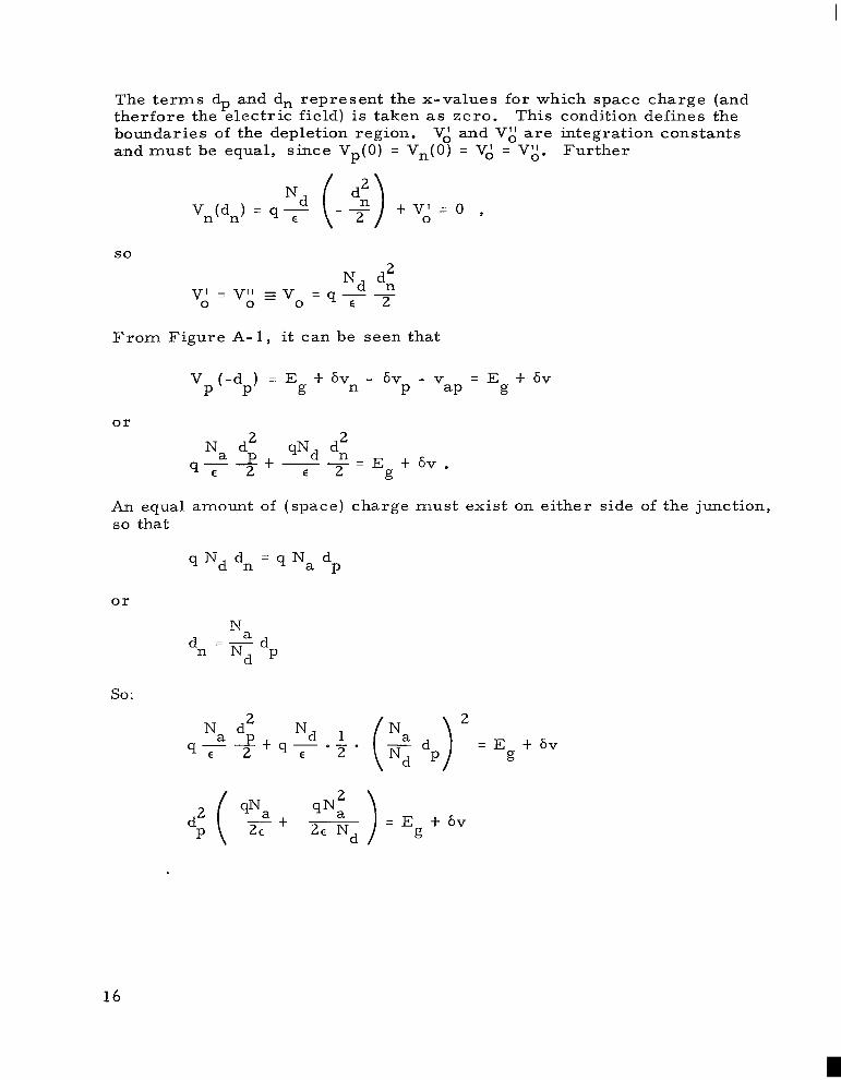
The t e rms dp and dn represent the x-values for which space charge (and therfore the electr ic field) i s taken a s zero. boundaries of the depletion region. andmust be equal, since V (0) = Vn(0) = Vd = V"
This condition defines the Vd and Vg a r e integration constants
Further P 0'
s o
F r o m Figure A- 1, it can be seen that
or
qf -$ !+- -=E N d2 qNd '2 t 6 ~ . g € 2
An equal amount of (space) charge must exist on either side of the junction, so that
or
so : 2 2
q - - t q - Na dp Nd E 4 7 - 1 ( 2 d p ) = E g t 6 v € 2
16

D I
and
d P =J..c...'.., NaNd + Na Nd
with the total width of the depletion region d = d, t %, and the junction ca- pacitance C = AE/d.
The tunneling distance, for ca r r i e r s of a particular energy, i s % - xp, with xp generally negative. For -d < x < 0, the expression for the top of the p-region valence band is:
This distance exists only in the range 6 v > 0.
P
and for the bottom of the n-region conduction band:
Nd ( $ - d n x ) + q - - - . Nd dz € 2 v (x) = -q 7 n
For 6vq, a particular determined f r o m
vP(x) - E g =
and
value of V, with 0 < 6vo < 6v, % and xp a r e implicitly
Nd '') P P Na 2 g
t-- - E 0
17
I

o r rewriting:
N 2 = o a
2 X
J + d x + 2 P P
so
(The cor rec t signs for the radic iting cases . ) Thus:
1s
0 < 6v < 6v 0
re determined by co sideration of lim-
t = d - (-dp) - / i t r Nd d 2 - - 26 (E t 6vo) - n n qNa g a
For specified mater ia ls and doping, the degeneracy (6v and 6v i s l inearly related to the applied voltage. rent, one can now integrate over V f r o m zero to 6v, with tunnel distance t being a known function of potential. An "average" tunnel distance can also be determined. This quantity i s somewhat arbi t rary; in this program it is defined by
and 6vn) i s known, To cayculate the tunnel cur-
t = L 6V 7 t (v) dv.
0
18

APPENDIX I1
NUMERICAL DETERMINATION O F FIRST AND SECOND DERIVATIVES
Consider a function f(x), known at a set of equally spaced points X-k, x-(k- 1 1, . . . x- 1 , xo, xi, . . . xk, with fk = f(xk). differences" of various order a s follows:
One can define "central
6 2 fo =z 1 ( 6 f l - 6f ) = f - 1 1 -1 - 2fo 4- f
3 1 2 2 1 2 2 - f - 2 ) - ( f l - f -1) 6 f = + f - 6 f ) = - ( f
0 1 -1
4 1 3 3 6 f = - ( 6 f - 6 f 1 ) = 6fo - 4fl - 4f-l t f 2 + f - 2 . 0 2 1 -
As shown in standard references on numerical analysis (ref. 11-1), the f i r s t and second derivatives of f, evaluated a t xo, a r e then given by
+ t e rms of higher order
2 f o - 1 2 6 4 f ) 0
h2 + t e rms of higher order
"k - xk-1' with h =
These expressions a r e used in the diode computer program, with h = 1 m V .
Electronics Research Center National Aeronautics and Space Administration
Cambridge, Massachusetts, November 1967 125 -2 1 -03 - 11
II- 1: Hildebrand, F. B. : Introduction to Numerical Analysis, McGraw-Hill, 1956.
I II
National Aeronautics and Space A W a b n WASHINGTON, D. C.
OFFICIAL BUSINESS -
FIRST CLASS MAIL POSTAGE AND FEES PAIL3
SPACE ADUlNISlRATION '' NATIONAL AERONAUTICS AND
POSTMASTER: If Undeliverable (Section 158 Postal Manual) Do Not Return.
"The aeronautical and space actiuities of the United States shall be conducted so as to contribute . . . to the expansion of human knowl- edge of phenomena in the atmosphere and space. The Administration shall provide for the widest practicable and appropriate dissemination of information concerning its activities and the results tbereof ."
-NATIONAL AERONAUTICS AND SPACE ACT OF 1958
NASA SCIENTIFIC AND TECHNICAL PUBLICATIONS
TECHNICAL REPORTS: Scientific and technical information considered important, complete, and a lasting contribution to existing .knowldge.
TECHNICAL NOTES: Information less broad in scope but nevertheless of importance as a contribution to existing knowledge.
TECHNICAL MEMORANDUMS: Information receiving limited distribu- tion because of preliminary data, security classification, or other reasons.
CONTRACTOR REPORTS: Scientific and technical information generated under a NASA contract or grant and considered an important contribution to existing knowledge.
TECHNICAL TRANSLATIONS: Information published in a foreign language considered to merit NASA distribution in English.
SPECIAL PUBLICATIONS: Information derived from or of value to NASA activities. Publications include conference proceedings, monographs, data compilations, handbooks, sourcebooks, and special bibliographies.
TECHNOLOGY UTILIZATION PUBLICATIONsj Information on tech- nology used by NASA that may be of particular interest in commercial and other non-aerospace applications. Publications indude Tech Briefs, Technology Utilization Reports and Notes, and Technology Surveys.
lk ta i ls on the availability of these publications may be obtained from:
SCIENTIFIC AND TECHNICAL INFORMATION DIVISION
NATIONAL AERONAUTICS AND SPACE ADMINISTRATION
Washington, D.C. PO546