characterisation of carbon nano-onions using raman spectroscopy
TRANSCRIPT
Characterisation of carbon nano-onions usingRaman spectroscopy
D. Roy a, Manish Chhowalla b,*, H. Wang c, N. Sano c, I. Alexandrou c,T.W. Clyne a, G.A.J. Amaratunga c
a Department of Materials Science, University of Cambridge, Pembroke Street, Cambridge CB2 3QZ, UKb Rutgers University, Ceramic and Materials Engineering, 607 Taylor Road, Piscataway, NJ 08854, USA
c Engineering Department, University of Cambridge, Trumpington Street, Cambridge CB2 1PZ, UK
Received 12 December 2002; in final form 25 March 2003
Abstract
Characteristics of the Raman spectrum from carbon onions have been identified in terms of the position of the G
peak and appearance of the transverse optic phonon peaks. Five new peaks were observed in the low wavenumber
region, at about 1100, 861, 700, 450 and 250 cm�1. The origins of these peaks are discussed in terms of the phonon
density of states (PDOS) and phonon dispersion curves of graphite. The curvature of the graphene planes is invoked to
explain the relaxation of the Raman selection rules and the appearance of the new peaks. The Raman spectrum of
carbon onions is compared with that of highly oriented pyrolytic graphite (HOPG). The strain of graphene planes due
to curvature has been estimated analytically and is used to account for the downward shift of the G peak.
� 2003 Elsevier Science B.V. All rights reserved.
1. Introduction
Since the discovery of fullerenes [1] and carbon
nanotubes [2], there have been intensive efforts toproduce and characterise nano-structured carbon
materials, with the main objective being to exploit
their properties for electronic and mechanical ap-
plications. Examples of nano-structured carbon
include nanotubes, nano-onions and nano-cones.
Transmission electron microscopy (TEM), electron
energy loss spectroscopy (EELS), Raman spec-
troscopy and scanning electron microscopy (SEM)are generally used to characterise these structures.
Of these, Raman spectroscopy is the most useful
non-destructive technique capable of differentiating
between these various structures [3–7]. Raman
spectra of diamond [4,8], graphite [3,7] and carbonnanotubes [5,9] arewell understood.However, there
are very few reports on Raman spectroscopy of
carbon nano-onions [6,10], with no report hitherto
of Raman features specific to carbon nano-onions.
In this Letter, characteristics of Raman spectra
from carbon nano-onions are reported.
2. Experimental procedures
The nano-onions used in this work were pro-
duced by applying a DC voltage across two
Chemical Physics Letters 373 (2003) 52–56
www.elsevier.com/locate/cplett
* Corresponding author. Fax: +1-732-445-3258.
E-mail address: [email protected] (M. Chhowalla).
0009-2614/03/$ - see front matter � 2003 Elsevier Science B.V. All rights reserved.
doi:10.1016/S0009-2614(03)00523-2
graphite electrodes submerged in water, generating
an arc discharge between them [11]. The discharge
current and voltage were 30 A and 16–17 V, re-
spectively. The nano-onions were mostly found
floating on the surface of the water. TEM inves-
tigation was performed with a JEOL 4000 EXtransmission electron microscope operated at
400 kV. The TEM specimen was prepared by
dipping the holey carbon grid into the water and
scooping out the onions from the surface. Raman
measurements were taken with three different wave
length of laser (514.5, 633, 785 nm) using a Reni-
shaw Raman microscope (Model-1000), covering
the spectral range of 200–1800 cm�1.
3. Results
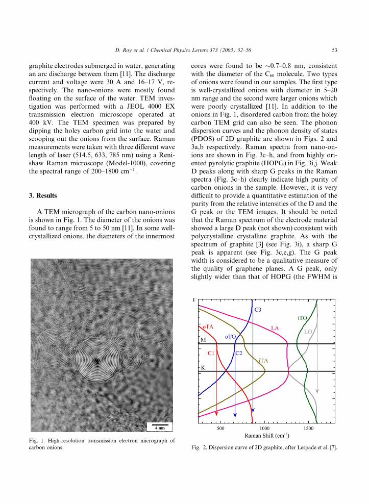
A TEM micrograph of the carbon nano-onions
is shown in Fig. 1. The diameter of the onions was
found to range from 5 to 50 nm [11]. In some well-
crystallized onions, the diameters of the innermost
cores were found to be �0.7–0.8 nm, consistent
with the diameter of the C60 molecule. Two types
of onions were found in our samples. The first type
is well-crystallized onions with diameter in 5–20
nm range and the second were larger onions which
were poorly crystallized [11]. In addition to theonions in Fig. 1, disordered carbon from the holey
carbon TEM grid can also be seen. The phonon
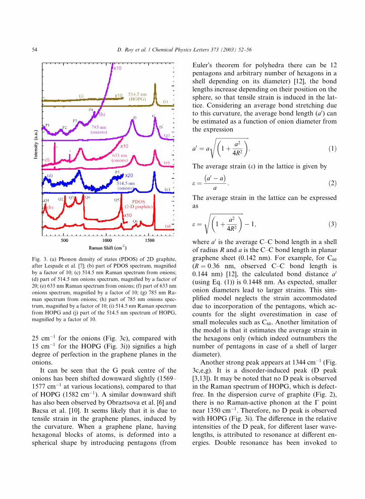
dispersion curves and the phonon density of states
(PDOS) of 2D graphite are shown in Figs. 2 and
3a,b respectively. Raman spectra from nano-on-
ions are shown in Fig. 3c–h, and from highly ori-
ented pyrolytic graphite (HOPG) in Fig. 3i,j. Weak
D peaks along with sharp G peaks in the Ramanspectra (Fig. 3c–h) clearly indicate high purity of
carbon onions in the sample. However, it is very
difficult to provide a quantitative estimation of the
purity from the relative intensities of the D and the
G peak or the TEM images. It should be noted
that the Raman spectrum of the electrode material
showed a large D peak (not shown) consistent with
polycrystalline crystalline graphite. As with thespectrum of graphite [3] (see Fig. 3i), a sharp G
peak is apparent (see Fig. 3c,e,g). The G peak
width is considered to be a qualitative measure of
the quality of graphene planes. A G peak, only
slightly wider than that of HOPG (the FWHM is
Fig. 1. High-resolution transmission electron micrograph of
carbon onions. Fig. 2. Dispersion curve of 2D graphite, after Lespade et al. [7].
D. Roy et al. / Chemical Physics Letters 373 (2003) 52–56 53
25 cm�1 for the onions (Fig. 3c), compared with
15 cm�1 for the HOPG (Fig. 3i)) signifies a high
degree of perfection in the graphene planes in the
onions.
It can be seen that the G peak centre of the
onions has been shifted downward slightly (1569–1577 cm�1 at various locations), compared to that
of HOPG (1582 cm�1). A similar downward shift
has also been observed by Obraztsova et al. [6] and
Bacsa et al. [10]. It seems likely that it is due to
tensile strain in the graphene planes, induced by
the curvature. When a graphene plane, having
hexagonal blocks of atoms, is deformed into a
spherical shape by introducing pentagons (from
Euler�s theorem for polyhedra there can be 12
pentagons and arbitrary number of hexagons in a
shell depending on its diameter) [12], the bond
lengths increase depending on their position on the
sphere, so that tensile strain is induced in the lat-
tice. Considering an average bond stretching dueto this curvature, the average bond length (a0) can
be estimated as a function of onion diameter from
the expression
a0 ¼ a
ffiffiffiffiffiffiffiffiffiffiffiffiffiffiffiffiffiffiffiffiffiffiffiffi1 þ a2
4R2
� �s: ð1Þ
The average strain (e) in the lattice is given by
e ¼a0 � a� �
a: ð2Þ
The average strain in the lattice can be expressedas
e ¼
ffiffiffiffiffiffiffiffiffiffiffiffiffiffiffiffiffiffiffiffiffiffiffiffi1 þ a2
4R2
� �s� 1; ð3Þ
where a0 is the average C–C bond length in a shell
of radius R and a is the C–C bond length in planar
graphene sheet (0.142 nm). For example, for C60
(R ¼ 0:36 nm, observed C–C bond length is
0.144 nm) [12], the calculated bond distance a0
(using Eq. (1)) is 0.1448 nm. As expected, smaller
onion diameters lead to larger strains. This sim-
plified model neglects the strain accommodated
due to incorporation of the pentagons, which ac-
counts for the slight overestimation in case of
small molecules such as C60. Another limitation of
the model is that it estimates the average strain in
the hexagons only (which indeed outnumbers thenumber of pentagons in case of a shell of larger
diameter).
Another strong peak appears at 1344 cm�1 (Fig.
3c,e,g). It is a disorder-induced peak (D peak
[3,13]). It may be noted that no D peak is observed
in the Raman spectrum of HOPG, which is defect-
free. In the dispersion curve of graphite (Fig. 2),
there is no Raman-active phonon at the C pointnear 1350 cm�1. Therefore, no D peak is observed
with HOPG (Fig. 3i). The difference in the relative
intensities of the D peak, for different laser wave-
lengths, is attributed to resonance at different en-
ergies. Double resonance has been invoked to
Fig. 3. (a) Phonon density of states (PDOS) of 2D graphite,
after Lespade et al. [7]; (b) part of PDOS spectrum, magnified
by a factor of 10; (c) 514.5 nm Raman spectrum from onions;
(d) part of 514.5 nm onions spectrum, magnified by a factor of
20; (e) 633 nm Raman spectrum from onions; (f) part of 633 nm
onions spectrum, magnified by a factor of 10; (g) 785 nm Ra-
man spectrum from onions; (h) part of 785 nm onions spec-
trum, magnified by a factor of 10; (i) 514.5 nm Raman spectrum
from HOPG and (j) part of the 514.5 nm spectrum of HOPG,
magnified by a factor of 10.
54 D. Roy et al. / Chemical Physics Letters 373 (2003) 52–56
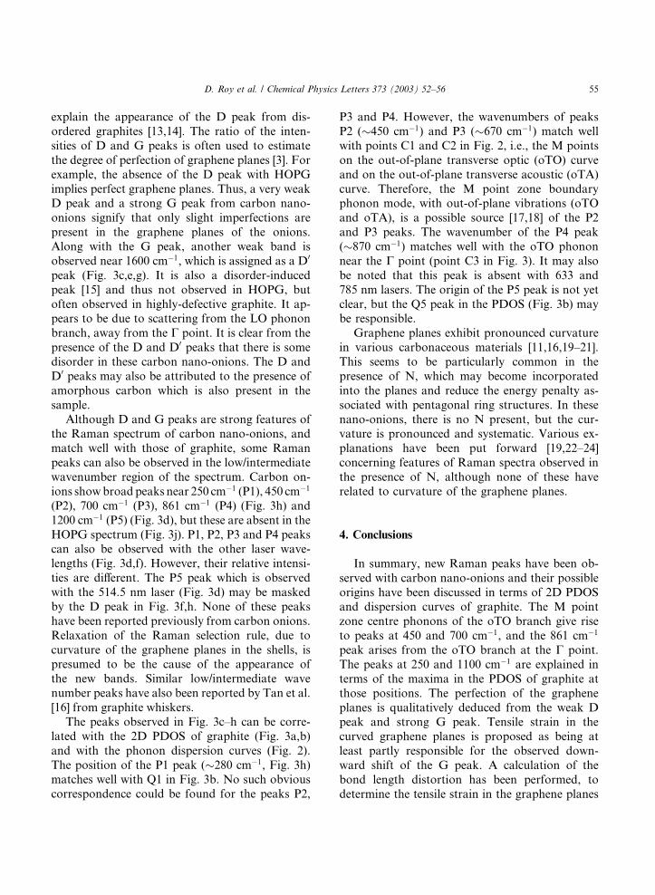
explain the appearance of the D peak from dis-
ordered graphites [13,14]. The ratio of the inten-
sities of D and G peaks is often used to estimate
the degree of perfection of graphene planes [3]. For
example, the absence of the D peak with HOPG
implies perfect graphene planes. Thus, a very weakD peak and a strong G peak from carbon nano-
onions signify that only slight imperfections are
present in the graphene planes of the onions.
Along with the G peak, another weak band is
observed near 1600 cm�1, which is assigned as a D0
peak (Fig. 3c,e,g). It is also a disorder-induced
peak [15] and thus not observed in HOPG, but
often observed in highly-defective graphite. It ap-pears to be due to scattering from the LO phonon
branch, away from the C point. It is clear from the
presence of the D and D0 peaks that there is some
disorder in these carbon nano-onions. The D and
D0 peaks may also be attributed to the presence of
amorphous carbon which is also present in the
sample.
Although D and G peaks are strong features ofthe Raman spectrum of carbon nano-onions, and
match well with those of graphite, some Raman
peaks can also be observed in the low/intermediate
wavenumber region of the spectrum. Carbon on-
ions showbroadpeaks near 250 cm�1 (P1), 450 cm�1
(P2), 700 cm�1 (P3), 861 cm�1 (P4) (Fig. 3h) and
1200 cm�1 (P5) (Fig. 3d), but these are absent in the
HOPG spectrum (Fig. 3j). P1, P2, P3 and P4 peakscan also be observed with the other laser wave-
lengths (Fig. 3d,f). However, their relative intensi-
ties are different. The P5 peak which is observed
with the 514.5 nm laser (Fig. 3d) may be masked
by the D peak in Fig. 3f,h. None of these peaks
have been reported previously from carbon onions.
Relaxation of the Raman selection rule, due to
curvature of the graphene planes in the shells, ispresumed to be the cause of the appearance of
the new bands. Similar low/intermediate wave
number peaks have also been reported by Tan et al.
[16] from graphite whiskers.
The peaks observed in Fig. 3c–h can be corre-
lated with the 2D PDOS of graphite (Fig. 3a,b)
and with the phonon dispersion curves (Fig. 2).
The position of the P1 peak (�280 cm�1, Fig. 3h)matches well with Q1 in Fig. 3b. No such obvious
correspondence could be found for the peaks P2,
P3 and P4. However, the wavenumbers of peaks
P2 (�450 cm�1) and P3 (�670 cm�1) match well
with points C1 and C2 in Fig. 2, i.e., the M points
on the out-of-plane transverse optic (oTO) curve
and on the out-of-plane transverse acoustic (oTA)
curve. Therefore, the M point zone boundaryphonon mode, with out-of-plane vibrations (oTO
and oTA), is a possible source [17,18] of the P2
and P3 peaks. The wavenumber of the P4 peak
(�870 cm�1) matches well with the oTO phonon
near the C point (point C3 in Fig. 3). It may also
be noted that this peak is absent with 633 and
785 nm lasers. The origin of the P5 peak is not yet
clear, but the Q5 peak in the PDOS (Fig. 3b) maybe responsible.
Graphene planes exhibit pronounced curvature
in various carbonaceous materials [11,16,19–21].
This seems to be particularly common in the
presence of N, which may become incorporated
into the planes and reduce the energy penalty as-
sociated with pentagonal ring structures. In these
nano-onions, there is no N present, but the cur-vature is pronounced and systematic. Various ex-
planations have been put forward [19,22–24]
concerning features of Raman spectra observed in
the presence of N, although none of these have
related to curvature of the graphene planes.
4. Conclusions
In summary, new Raman peaks have been ob-
served with carbon nano-onions and their possible
origins have been discussed in terms of 2D PDOSand dispersion curves of graphite. The M point
zone centre phonons of the oTO branch give rise
to peaks at 450 and 700 cm�1, and the 861 cm�1
peak arises from the oTO branch at the C point.
The peaks at 250 and 1100 cm�1 are explained in
terms of the maxima in the PDOS of graphite at
those positions. The perfection of the graphene
planes is qualitatively deduced from the weak Dpeak and strong G peak. Tensile strain in the
curved graphene planes is proposed as being at
least partly responsible for the observed down-
ward shift of the G peak. A calculation of the
bond length distortion has been performed, to
determine the tensile strain in the graphene planes
D. Roy et al. / Chemical Physics Letters 373 (2003) 52–56 55

induced by curvature. Therefore, a strong G peak
with a wavenumber below that of HOPG, and
certain intermediate wave number peaks, both
appear to be characteristic features of the Raman
spectrum of carbon onions.
Acknowledgements
D. Roy gratefully acknowledges financial sup-port from Nehru Trust for Cambridge University
(India) and CVCP (UK).
References
[1] H. Kroto, J.R. Heath, S.C. O�Brien, R.F. Curl, R.E.
Smalley, Nature 318 (1985) 162.
[2] S. Iijima, Nature 354 (1991) 56.
[3] F. Tuinstra, J.L. Koenig, J. Chem. Phys. 53 (1970) 1126.
[4] S.A. Solin, A.K. Ramdas, Phys. Rev. B 1 (1970) 1687.
[5] A.M. Rao et al., Science 275 (1997) 187.
[6] E.D. Obraztsova et al., Carbon 36 (1998) 821.
[7] L. Lespade, R. Al-Jishi, M.S. Dresselhaus, Carbon 20
(1982) 427.
[8] R.J. Nemanich, J.T. Glass, G. Lucovsky, R.E. Shroder,
J. Vac. Sci. Technol. A 6 (1988) 1783.
[9] G.S. Duesberg, L. Loa, M. Burghard, K. Syassen, S. Roth,
Phys. Rev. B 85 (2000) 5436.
[10] W.S. Bacsa, W.A. de Heer, D. Ugarte, A. Chatelain,
Chem. Phys. Lett. 211 (1993) 346.
[11] N. Sano, H. Wang, M. Chhowalla, I. Alexandrou, G.A.J.
Amaratunga, Nature 414 (2001) 506;
Sano et al., J. Appl. Phys. 92 (2002) 2783.
[12] M.S. Dresselhaus, G. Dresselhaus, P.C. Eklund, Science of
Fullerines and Carbon Nanotubes, Academic Press, New
York, 1996.
[13] C. Thomsen, S. Reich, Phys. Rev. Lett. 85 (2000) 5214.
[14] R. Saito et al., Phys. Rev. Lett. 88 (2002) 027401(1–4).
[15] A.M. Rao et al., Phys. Rev. Lett. 84 (2000) 1820.
[16] P.H. Tan, C.Y. Hu, J. Dong, W.C. Shen, B.F. Zhang,
Phys. Rev. B 64 (2001).
[17] R.J. Nemanich, S.A. Solin, Phys. Rev. B 20 (1979) 392.
[18] R. Al-Jishi, G. Dresselhaus, Phys. Rev. B. 26 (1982)
4514.
[19] S.E. Rodil, A.C. Ferrari, J. Robertson, W.I. Milne, J.
Appl. Phys. 89 (2001) 5425.
[20] N. Hellgren et al., Phys. Rev. B. 59 (1999) 5162.
[21] N. Hellgren et al., J. Vac. Sci. Technol. A 18 (2000) 2349.
[22] S. Kumar, T.L. Tansley, Thin Solid Films 256 (1995) 44.
[23] F. Li, J.S. Lannin, Appl. Phys. Lett. 61 (1992) 2116.
[24] M.A. Tamor, W.C. Vassel, J. Appl. Phys. 76 (1994)
3823.
56 D. Roy et al. / Chemical Physics Letters 373 (2003) 52–56