chapter two power semiconductor diodes and circuits designed by dr. sameer khader ppu “e-learning...
TRANSCRIPT

CHAPTER TWO
POWER SEMICONDUCTOR DIODESAND CIRCUITS
DESIGNED BY
DR. SAMEER KHADERPPU
“E-learning Project”

Diode circuits
I- (S.2.3) : Diode Characteristics: Power diode is a two-terminal pn-junction device ……….);The equivalent circuit and i-v curve are displayed as follows, where the diode conducts when a battery is connected across its terminals .
Symbol
P-N junction P-N junction
;qT.KVT
voltagethermalV
currentleakageI
voltagediodeVwhere
)1e(II
T
s
D
V.nVsD
TD

II- (S.2.4) : Reverse Recovery Characteristics: When the current falls to zero , the diode continues to conduct under the action of minority carriers that remain stored in the pn-junction and Bulk resistance. These carriers require a certain time to recombine with opposite charges and to be neutralized. This time is called the reverse recovery time trr . The figure shown below displayed the current falling process and the diode reverse parameters.
.di/dttI , tt t
.dt .Q.di.t t; .di/dt t trr
2.Q I
.tI
.tI
.tI Q
arrbarr
rr2rraarr
rr
2
rrrr
2
brr
2
arrrr
1- The reverse recovery time trr consist
of two parameters ta, and tb: trr =ta+tb ; Irr=ta.di/dt ta- due to storage charge in the depletion regiontb- due to storage charge in the bulk resistance.The softness factor Sf=tb/ta.Trr- depends on the junction temperature, di/dt, and the diode forward current
2- The reverse recovery charge Qrr : this is the charge carriers across the diode flows in the reverse direction due to changeover of the conduction state.
;2;/2
/2
.
2
tirrrr
rrrr
rrr
ddQIdtdi
Qt
dtdiQrttrrtatatb

Example 2.1: Given a diode circuit (p.2.1) with reverse recovery time trr=5 µS, and the rate of fall of the diode current is di/dt= 80A/ µS with softness factor Sf=0.5. Determine : 1- the storage charge Qrr; 2- the peak reverse current Irr.
Solution:
C6.133310.5*72.266t.IQ
A72.26610/80*10334.3d
d.tI
s10334.310.5t
t
tttt
t5.0S
5
2
1rrrr
2
1rr
66
t
iarr
6
5.1
6
5.1
rra
barra
bF
III- (S.2.5) : Diodes Classification : Depending on the recovery characteristics, and manufacturing techniques, there are three types:
1. General - purpose diodes: they have high trr=25 µS and with frequency < 1kHZ, applied in AC to DC circuits. The current rating up to 1000A, and up to 5kV.
2. Fast recovery diodes: they have small trr=5 µS and with frequency < 5kHZ, applied in DC to DC and DC to AC circuits. The current rating up to 100A, and up to3kV.

3. Schottkey diode: they have approximately zero reverse recovery time with high frequency up to 10kHz, and applied in high current low voltage applications. The current rating up to 300A and 100V circuit voltage.
IV- (S.2.8) : Series –Connected Diodes : In high voltage dc applications (mainly), the diodes are connected in series with purpose to
increase the reverse blocking capabilities.The difference in the i-v curve in the reverse blocking condition occurs due to manufacturing
errors and tolerances, therefore each diode should carry different voltage , while the leakage current is the same.
The solution is to force equal sharing voltage across the diodes by connecting a sharing resistances as well shown below:
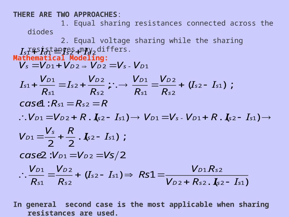
THERE ARE TWO APPROACHES: 1. Equal sharing resistances connected across the diodes 2. Equal voltage sharing while the sharing resistances may differs. Mathematical Modeling:
).(1)(
2:2
);.(22
).().(
:1
);(;
1222
2.112
2
2
1
1
21
121
12111221
21
122
2
1
1
2
22
1
11
1221
2211
sssD
sDss
s
D
s
D
DD
sss
D
ssDsDssDD
ss
sss
D
s
D
s
Ds
s
Ds
DsDDDs
dsds
IIRV
RVRsII
R
V
R
V
VsVVcase
IIRV
V
IIRVVVIIRVV
RRRcase
IIR
V
R
V
R
VI
R
VI
VVVVVV
IIII
In general second case is the most applicable when sharing resistances are used.

Example 2.2: Two diodes are connected in series as well shown on up mentioned circuit, where the circuit parameters are: 7kV source voltage ( DC) , leakage current of first diode Is1=40mA and of second diode Is2=50mA . 1- Find the diode voltages if the resistances are equals Rs1=Rs2=R=80 kΩ. 2- Find the sharing resistances if the diode voltages are distributed equally.
Solution: Two cases must be described as follow Case#1: Rs1=Rs2=R=80 kΩ
k702Rsand;k34.581Rs
k34.58310.10.700003500
70000.35001Rsk702RsLet
V35002VsVV:2case
V3100VVsV
V3900310).4050.(2
80000
2
7000)II.(
2
R
2
VV
2D1D
1D2D
1s2ss
1D

V- (S.2.9) : Parallel –Connected Diodes : In high power applications, diodes are connected in parallel with purpose to increase the
current carrying capability. Due to some differences in the Bulk resistances of both diodes, there is a different current will flow through the diodes. Therefore by connecting resistances in series with the diodes the diode voltage is shared equally as well shown below:
The function of both Ls1 and Ls2 is to equally sharing the current under dynamic behaviors.When ID1 rises, the inductor voltage Ls1.d(Id1)/dt increases, and a corresponding voltage of opposite polarity is induced across inductor Ls2. This resulting low impedance in the circuit of D2, therefore shifting the current to flow through D2 path.

Mathematical Modeling: The following equation are derived under steady-state conditions
1D2D
2D1D
2D1D1D2D2s1s
2D4s2D1D3s1D
;42D31D
II
VVR
VV)II(RRRRLet
I.RVI.RV
VVVV
Example 2.3: Find the value of R required for adjusting the voltage across the diodes D1 and D2, if ID1=50A, ID= 95A, VD1=1.8V, and VD2=2V.
Solution:
m205045
28.1
II
VVR
A455095IIIIII
1D2D
2D1D
1DD2D2D1DD

Mode#1 D1 conducts: The current will flow from the source to the load through D1, where the current i1:
IV- (S.2.12) : Freewheeling Diodes If switch S in the figure shown below is closed for time t1, a current I1 is established through
the load; and then if the switch is opened for time t2 the current continues to flow through the inductor and the diode” closed path’. If there in no closed path the inductive energy induces a very high voltage and this energy is dissipated in form of heat and spark. The diode realized closed path is called usually FREEWHEELING DIODE.
The operation of the proposed circuit is divided into two modes:
RLeVstV
eR
Vti
dt
diLiRV
tL
tss
/;.)(
)1()(. 11
1

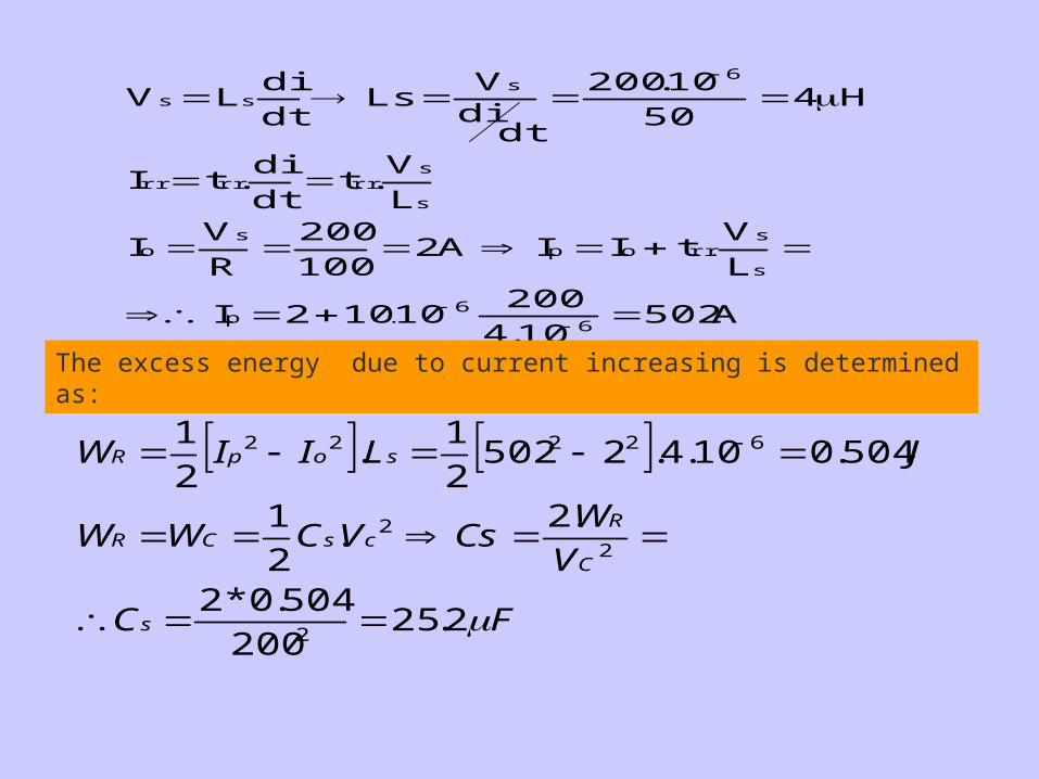
Example 2.4: Determine the value of Ls and Cs for the diode circuit shown behind with L=5mH;
R=100Ω; Vs=200V; and di/dt = 50A/ µS . Solution: by applying Lenz law the circuit
inductance Ls is determined as follows:
Mode#2 Dm conducts: The current will continue to flow through the load and the diode Dm., where the current i2:
t12
11
ts1
11
e.I)t(i
;R
VsIIttAt
)e1(R
V)t(i
dt
diLi.R0
A50210.4
20010102I
L
VtIIA2
100
200
R
VI
L
V.t
dt
di.tI
H450
10.200
dtdiV
Lsdt
diLV
66
.p
s
s.rrop
so
s
srrrrrr
6s
ss
The excess energy due to current increasing is determined as:
FC
V
WCsVCWW
JLIIW
s
C
RcsCR
sopR
2.25200
504.0*2
.2.
2
1
504.010.4.25022
1.
2
1
2
22
62222
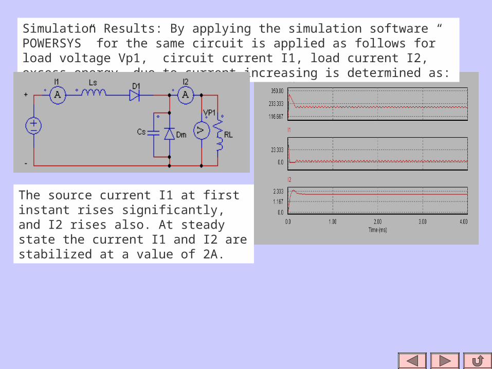
Simulation Results: By applying the simulation software “ POWERSYS” for the same circuit is applied as follows for load voltage Vp1, circuit current I1, load current I2, excess energy due to current increasing is determined as:
The source current I1 at first instant rises significantly, and I2 rises also. At steady state the current I1 and I2 are stabilized at a value of 2A.

THANK YOU FOR LISTENING
QUESTIONS…..?
PLEASE DON’T HESTATE TO CONTACT ME
BY EMAIL ON