chapter 8 delaminated film buckling microchannels
TRANSCRIPT

Chapter 8
Delaminated Film Buckling Microchannels
Alex A. Volinsky and Patrick Waters
Abstract This chapter describes the method of manufacturing microfluidic
microchannels formed by delaminated buckled thin films. Thin films under com-
pression tend to delaminate and buckle. Microchannel geometry can be controlled
by tailoring film residual stress and placing patterned adhesion-weakening layers
utilizing photolithographic techniques. Results based on the photoresist as the
adhesion weakening layer and compressed tungsten thin films are described along
with the corresponding thin film mechanics.
8.1 Introduction
Buckling delamination blisters are commonly observed in compressed thin films.
These mechanically active features arise from a local loss of adhesion between the
film and the substrate, due to the relief of residual stress, and exhibit directional
growth. Thin films in compression can also develop circular, asterisk, straight, and
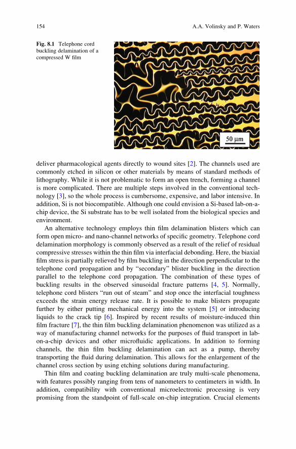
phone-cord blisters. “Telephone cords” are wormlike buckled features observed in
thin films, and are called so because they look like a twisted phone cord when they
are viewed under an optical microscope (Fig. 8.1). The geometry and path of these
blisters can be controlled by placing adhesion-weakening layers, thereby outlining
the desired in-plane blister configuration and forming a channel network on a chip.
Microfluidics, as a field, has been growing with the new advances in nanotech-
nology [1]. This field is estimated to grow at an exponential rate, and is expected to
continue to do so in the decades to come. This relatively new technology has
different possible applications, from sensors to drug delivery. It relies on the ability
to transfer fluids at small-scale chip sizes. Recently these were successfully used to
A.A. Volinsky (*) • P. Waters
Department of Mechanical Engineering, University of South Florida,
4202 E Fowler Ave ENB118, Tampa, FL 33620, USA
e-mail: [email protected]
X. Chen (ed.), Mechanical Self-Assembly: Science and Applications,DOI 10.1007/978-1-4614-4562-3_8, # Springer Science+Business Media New York 2013
153
deliver pharmacological agents directly to wound sites [2]. The channels used are
commonly etched in silicon or other materials by means of standard methods of
lithography. While it is not problematic to form an open trench, forming a channel
is more complicated. There are multiple steps involved in the conventional tech-
nology [3], so the whole process is cumbersome, expensive, and labor intensive. In
addition, Si is not biocompatible. Although one could envision a Si-based lab-on-a-
chip device, the Si substrate has to be well isolated from the biological species and
environment.
An alternative technology employs thin film delamination blisters which can
form open micro- and nano-channel networks of specific geometry. Telephone cord
delamination morphology is commonly observed as a result of the relief of residual
compressive stresses within the thin film via interfacial debonding. Here, the biaxial
film stress is partially relieved by film buckling in the direction perpendicular to the
telephone cord propagation and by “secondary” blister buckling in the direction
parallel to the telephone cord propagation. The combination of these types of
buckling results in the observed sinusoidal fracture patterns [4, 5]. Normally,
telephone cord blisters “run out of steam” and stop once the interfacial toughness
exceeds the strain energy release rate. It is possible to make blisters propagate
further by either putting mechanical energy into the system [5] or introducing
liquids to the crack tip [6]. Inspired by recent results of moisture-induced thin
film fracture [7], the thin film buckling delamination phenomenon was utilized as a
way of manufacturing channel networks for the purposes of fluid transport in lab-
on-a-chip devices and other microfluidic applications. In addition to forming
channels, the thin film buckling delamination can act as a pump, thereby
transporting the fluid during delamination. This allows for the enlargement of the
channel cross section by using etching solutions during manufacturing.
Thin film and coating buckling delamination are truly multi-scale phenomena,
with features possibly ranging from tens of nanometers to centimeters in width. In
addition, compatibility with conventional microelectronic processing is very
promising from the standpoint of full-scale on-chip integration. Crucial elements
Fig. 8.1 Telephone cord
buckling delamination of a
compressed W film
154 A.A. Volinsky and P. Waters

of a lab-on-a-chip device are channels capable of transporting the fluids within the
chip dimensions and an interface which is manipulatable from the outside world.
Channels allow various fluids to be mixed, stored, and passed through. Typical
fluids include blood, protein solutions in various buffers, cell suspensions, etc.
Several measurements can be performed by microfluidic devices, including fluid
viscosity and pH [8, 9].
The competitive advantage of the channel miniaturization is due to the fact that
the Reynolds number is low, allowing for laminar flow to prevail and convective
mixing of the fluids not to occur. Miniaturization of the channels, and their
integration onto a single chip, would allow for the handling of minute amounts of
sample material, thus increasing the sensitivity. The analyte concentration Ai is
inversely proportional to its volume, V, and is given in terms of the device
efficiency, �s, as in [1]
Ai ¼ 1
�sNAV; (8.1)
where NA is the Avogadro’s number. Reduction of the sample size provides higher
device sensitivity, as well as the capability of handling smaller samples. One can
easily and effectively perform immuno- and DNA probe assays by using minute
amounts of sample material.
In addition, the channel profile geometry has a substantial influence on the fluid
flow. It is important to know the distribution of the analytes in the channel for
developing functional and reproducible assays. One would want to increase the
molecule residence time for quantitative time-dependent analyses. The prediction
of the molecule residence time is a complicated task, as it depends on the molecule
location in the channel profile. A low-aspect-ratio channel velocity profile allows
lateral diffusion to occur in the vertical dimension without an accompanying
change in the residence time of the diffusing molecules. Therefore, one would
desire microchannels with low aspect ratios for accurate quantitative studies. Thin
film buckling channels have a low aspect ratio, i.e., height-to-width ratio.
8.2 Thin Film Buckling Delamination
Many industries, including microelectronics and microfluidics, depend on well-
adhered thin films. Thin films are normally stressed, with biaxial residual stress
residing in unpassivated films [10]. Stress in a thin film typically causes substrate
bending. This effect is employed in measuring the macroscopic residual stress
found within thin films by using Stoney’s equation [11]. There are many different
stress relief mechanisms observed in thin films. The residual stress can be partially
relieved by plastic deformation and surface reconstruction. It may also be more
completely relieved by mechanical film failure, especially if the stress levels are
high and/or externally applied stresses are present.
8 Delaminated Film Buckling Microchannels 155
Telephone cord delamination has been observed in various thin film systems,
including tungsten, carbon, diamond-like carbon (DLC), TaN, and other films which
have been applied upon various substrates [12–18]. Some theoretical considerations
of the formation of the telephone cord buckling geometry can be found in [19–22].
Most of the time delamination blisters run parallel to each other in blanket, non-
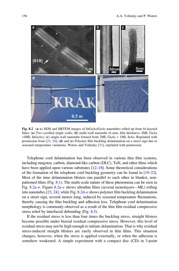
patterned films (Fig. 8.1). The multi-scale nature of these phenomena can be seen in
Fig. 8.2a–e. Figure 8.2a–c shows ultrathin films (several monolayers—ML) rolling
into nanotubes [23, 24], while Fig. 8.2d–e shows polymer film buckling delamination
on a street sign, several meters long, induced by seasonal temperature fluctuations,
thereby causing the film buckling and adhesion loss. Telephone cord delamination
morphology is commonly observed as a result of the thin film residual compressive
stress relief by interfacial debonding (Fig. 8.3).
If the residual stress is less than four times the buckling stress, straight blisters
become possible under biaxial residual compressive stress. However, this level of
residual stress may not be high enough to initiate delamination. That is why residual
stress-induced straight blisters are rarely observed in thin films. This situation
changes, however, when the stress is applied externally, or when the adhesion is
somehow weakened. A simple experiment with a compact disc (CD) in 3-point
Fig. 8.2 (a–c) SEM and HRTEM images of InGaAs/GaAs nanotubes rolled up from bi-layered
films: (a) Two scrolled single walls; (b) multi-wall nanotube (6 turn, film thickness: 4ML GaAs
+4ML InGaAs); (c) single-wall nanotube formed from 2ML GaAs + 1ML InAs. Reprinted with
permission from [23, 24]; (d) and (e) Polymer film buckling delamination on a street sign due to
seasonal temperature variations. Waters and Volinsky [31], reprinted with permission
156 A.A. Volinsky and P. Waters

bending has been described in [4] to support this. Detailed dynamics of real-time
telephone cord blister propagation can be observed online [25]. As was previously
stated, telephone cord blisters “run out of steam” and stop once the interfacial
toughness exceeds the strain energy release rate. It is possible to make blisters
propagate further by either putting mechanical energy into the system [5] or
introducing liquids at the crack tip [6, 7]. Liquids can also provide the mechanical
energy (through surface tension and capillary forces) needed to continue the blister
propagation and can also reduce the film interfacial toughness. These effects were
attributed to environmentally assisted cracking, which caused the thin film delami-
nation, and is similar to a commonly known example of the degradation and fading
of vintage mirrors, as well as solar mirrors [26]. If one were to use a substrate
etching solution as a fluid, then, in addition to causing thin film delamination, it
would etch the substrate, thereby enlarging the channel cross section.
Tests have been conducted that demonstrate the method of fluid introduction as a
means of propagating delamination blisters. These blisters continue to propagate
until the fluid has been removed, or until the delamination reaches the end of the
sample [6]. All of the samples contained a 1 mm thick W superlayer deposited on
either thin magnetic layers or 40 nm thick Cu films on Si substrates, with a
thermally grown SiO2 layer. Figure 8.4 shows two snapshots, taken 3 min apart,
illustrating water-induced blister propagation. The evidence of fluid transport is
presented in Fig. 8.5. Here, the buckling delamination propagated from the right to
the left, and the water, upon reaching the far left side of the sample, moved down
the edge of the Si wafer. This demonstrates one of the potential mechanisms of fluid
transport via blister propagation. In this case, water was transported, with the
advance of the crack tip, at about 10 mm/min, although higher propagation rates,
Fig. 8.3 Transition from
straight-sided blister to
sinusoidal shape
8 Delaminated Film Buckling Microchannels 157

up to several microns per second, were observed in other samples. It has been
previously shown that interfacial cracks in thin films act as a vacuum cleaner,
collecting contaminants from the atmosphere, thus reducing the energy of the newly
formed fracture surfaces [13, 14]. In this case, the crack is acting like a pump, thus
transporting the fluid along with the blister propagation. Water droplets can be seen
on the Si substrate in Fig. 8.5.
In order to make a microfluidic or lab-on-a-chip device, the placement of
delamination fluid transport channels needs to be exact and repeatable. Standard
lithographic techniques have demonstrated the ability to control the blister place-
ment and the buckling geometry [27]. Both telephone cord as well as straight blister
geometries are available and depend on the film stress level and the width of
the adhesion-weakening (release) layer [27]. With the use of moisture, the
requirements on the release layer adhesion properties are less stringent, as the stress
combined with the moisture is sufficient to cause delamination. The properties of
the internal walls of the channel can be altered by varying the underlying materials.
For example, it has been shown that fracture in low-K dielectric films is
Fig. 8.4 Water-induced blister growth. Volinsky et al. [7], reprinted with permission
Fig. 8.5 Water transport in the delaminated blister. Volinsky et al. [7], reprinted with permission
158 A.A. Volinsky and P. Waters

cohesive, i.e., the crack propagates in the film itself [28]. A similar effect is
expected for a polymer release layer and it may even be possible to use regular
photoresistant “lining” inside the channel. One could also use a biocompatible
material as an adhesion-weakening layer, which would include polymer and
ceramic films, as well as DLC.
Figure 8.6a shows two 50 mmwide straight channels, which coalesce by forming
a telephone cord delamination blister, resulting in a single 50 mmwide channel. The
profilometer scan in Fig. 8.6b reflects the blister buckling geometry. A highly
desirable microchannel aspect ratio of 1:25 is achieved here. This demonstrates
the possibility of constructing a fluid-mixing device by employing thin film buck-
ling channels. In this particular case, the double-to-single channel transition
occurred naturally, although the same result can be achieved with patterned release
layers, which form channel network structures. Another important example of a
storage element is shown in Fig. 8.7, where a channel extends to a larger reservoir.
Fig. 8.6 (a) Optical micrograph of two straight buckled channels coalescing into one through a
telephone cord delamination, and (b) corresponding height profiles. Volinsky et al. [7], reprinted
with permission
Fig. 8.7 Buckling delamination showing channels and fluid “storage reservoirs”
8 Delaminated Film Buckling Microchannels 159
One can envision using this storage element as a pump, when combined with an
electrostatic device capable of mechanically pressurizing it from the top.
8.3 Buckling Blister Mechanics
The buckling channel geometry can be predicted based on the multilayer material
properties, residual stress, and adhesion [22]. The steady-state interfacial toughness
of the film, in the direction of the blister propagation (shown in Fig. 8.6a), is
GSS ¼ ð1� n2Þhs2r2E
1� sBsr
� �2
; (8.2)
where sr and sB are the residual (compressive) stress and the buckling stress,
respectively, h is the film thickness, E is the elastic modulus, and n is the Poisson’sratio. The buckling stress is given in terms of the film thickness and the blister
width, b, as
sB ¼ p2
12
E
ð1� n2Þh
b
� �2
: (8.3)
Now one can express the residual stress in terms of the buckling stress and the
blister heights, d, as
sr ¼ 3
4sB
d2
h2þ 1
� �: (8.4)
To complete the formulation, the mode-dependent interfacial film toughness, in
the buckling direction, perpendicular to the blister propagation, can be expressed as
GðCÞ ¼ ð1� n2Þh2E
ðsr � sBÞðsr þ 3sBÞ: (8.5)
This simple analysis basically shows that the level of the residual stress and the
extent of the thin film adhesion will control the microchannel geometry. The upper
layer residual stress, determined primarily by the deposition parameters, will
control the microchannel height.
Typically, residual stress in thin films results in negative consequences that
include wafer bowing, film cracking, and delamination. However, depositing a
film with a compressive residual stress has been demonstrated to be a benefit,
specifically when using superlayer indentation to determine the thin film interfacial
toughness [12]. A similar concept can be employed to create microchannels. When
the strain energy release rate, G, exceeds the interfacial toughness, Гi, of a film/
160 A.A. Volinsky and P. Waters

substrate, delamination will occur. A simplified form of the strain energy release
rate in a stressed film is [22]
G ¼ Zs2f hEf
; (8.6)
where sf is the stress in the film, h is the film thickness, Ef is the modulus of
elasticity, and Z is a dimensionless parameter that depends on the geometry.
In thin film systems with biaxial compressive stresses, various shapes of the
delaminated regions will arise. These shapes include long straight-sided, circular,
and telephone cord delamination, which is the most commonly observed morphol-
ogy. The delamination shape and size will depend on factors such as the film stress,
thickness, and interfacial toughness. Most importantly, the propagation depends on
the interfacial toughness, which increases as the mode mixity, acting on the
interface ahead of the delamination crack, shifts from mode I towards mode II.
Interfacial failure starts with the film delaminating from the substrate and is
followed by the spreading of the delamination as the buckling loads the edge of
the interfacial crack, resulting in a failure phenomenon that couples both buckling
and interfacial crack propagation.
To create useful microchannels via film delaminations, the direction and mor-
phology of the delaminations need to be controlled. The easiest way to control
delamination is by controlling the interfacial toughness. This can be done by
creating adhesion-reducing layers that have a lower interfacial toughness than the
surrounding areas. A compressively stressed film can be used in conjunction with a
patterned adhesion-reducing layer as a method for creating microchannels. Using
delaminations will hopefully solve the existing challenges and provide an alterna-
tive method in creating microchannels.
8.4 Buckling Microchannel Pattern Manufacturing
To create the adhesion-reducing layers, standard photolithography techniques were
employed [29]. The simplest approach used the patterned photoresist as the adhe-
sion reducer. The basic steps in lithography include the following:
(1) The application of a photosensitive material (photoresist)
(2) Soft bake of the photoresist
(3) Exposure of the photoresist
(4) Development of the exposed pattern
(5) Hard bake of the remaining pattern
Figure 8.8 is a depiction of the basic lithography steps used here, along with the
additional step of depositing a compressively stressed film for creating
delamination-induced microchannels.
8 Delaminated Film Buckling Microchannels 161

There are two types of photoresist to choose from: positive and negative
photoresist. Positive photoresist is exposed to UV light wherever it is to be
removed. Regarding the positive photoresist, exposure to the UV light changes its
chemical structure so that it becomes more soluble in a developer, which is opposite
to that of the negative photoresist. The exposed photoresist is then washed away by
a developer solution, leaving areas of the underlying material bare. Therefore, the
mask contains an exact copy of the pattern, which is to remain on the wafer.
In general, positive photoresists provide clearer edge definition than negative
photoresists. The better edge definition found in positive photoresists makes them
a better option for high-resolution patterns.
Negative photoresists behave in the opposite manner. Exposure to the UV light
causes the negative photoresist to become polymerized, and consequently more
difficult to dissolve. Therefore, the negative photoresist remains on the surface
wherever it is exposed, and the developer solution removes only the unexposed
portions. Thus, masks used for negative photoresists contain the inverse of the
pattern to be transferred. Shipley 1813 was used here, which is a positive photore-
sist that is optimized for G-line exposure (436 nm wavelength).
Normally, to start the photoresist application process, the wafer surface is
prepared in a specific way in order to remove the surface moisture and other
contaminants. In order to remove the moisture, the wafers are baked and then
primed with an adhesion promoter. Hexamethyldisilazane (HMDS) is normally
used as the adhesion promoter and is applied at a reduced pressure to form a
monomolecular layer on the wafer surface, thereby making the wafer hydrophobic,
which prevents moisture condensation. These wafer preparation steps were ignored
here because the goal of the photoresist layer was to be an adhesion reducer and
only a proof of concept was intended.
Spin coating was used to apply the photoresist with thicknesses ranging from a
few hundred nanometers to a few microns. If thicker coatings are required, electro-
chemical coatings, spray coatings, and casting processes can be used [29].
A Laurell Technologies WS-400A-8NPP/Lite Spin Processor was utilized here
and can handle wafers up to 800 in diameter. It uses a vacuum chuck to hold the
Si wafer
Mask
ExposureSpin coating
Develop W deposition W delamination
Photoresist Soft bake
Hard bake
Fig. 8.8 Process of creating microchannels
162 A.A. Volinsky and P. Waters
wafers in place and has a spin speed which can range from 0 to 6,000 rpm.
Acceleration profiles, speed changes, and spin times can all be programmed by
the user. By adjusting the spin speed, the photoresist thickness can be controlled.
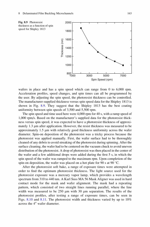
The manufacturer-supplied thickness versus spin speed data for the Shipley 1813 is
shown in Fig. 8.9. They suggest that the Shipley 1813 has the best coating
uniformity between spin speeds of 3,500 and 5,500 rpm.
The spin speed and time used here were 4,000 rpm for 40 s, with a ramp speed of
1,000 rpm/s. Based on the manufacturer’s supplied data for the photoresist thick-
ness versus spin speed, it was expected to have a photoresist thickness of approxi-
mately 1.3 mm after application. However, the resist thickness was measured to be
approximately 1.5 mm with relatively good thickness uniformity across the wafer
diameter. Spin-on deposition of the photoresist was a tricky process because the
photoresist was applied manually. First, the wafer surface had to be thoroughly
cleaned of any debris to avoid streaking of the photoresist during spinning. After the
surface cleaning, the wafer had to be centered on the vacuum chuck to avoid uneven
distribution of the photoresist. A drop of photoresist was then placed in the center of
the wafer and a few additional drops were added during the first 5 s, in which the
spin speed of the wafer was ramped to the maximum rpm. Upon completion of the
spin-on deposition, the wafer was placed on a hot plate for 90 s at 90 �C.After the photoresist soft bake, a range of exposure times were attempted in
order to find the optimum photoresist thickness. The light source used for the
photoresist exposure was a mercury vapor lamp, which provides a wavelength
spectrum from 310 to 440 nm. A Karl Suss MA 56 Mask Aligner was used in hard
contact mode for the mask and wafer alignment. The mask had a repeating
pattern, which consisted of two straight lines running parallel, where the line
width was measured to be 250 mm with 30 mm separation. The results of the
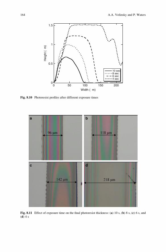
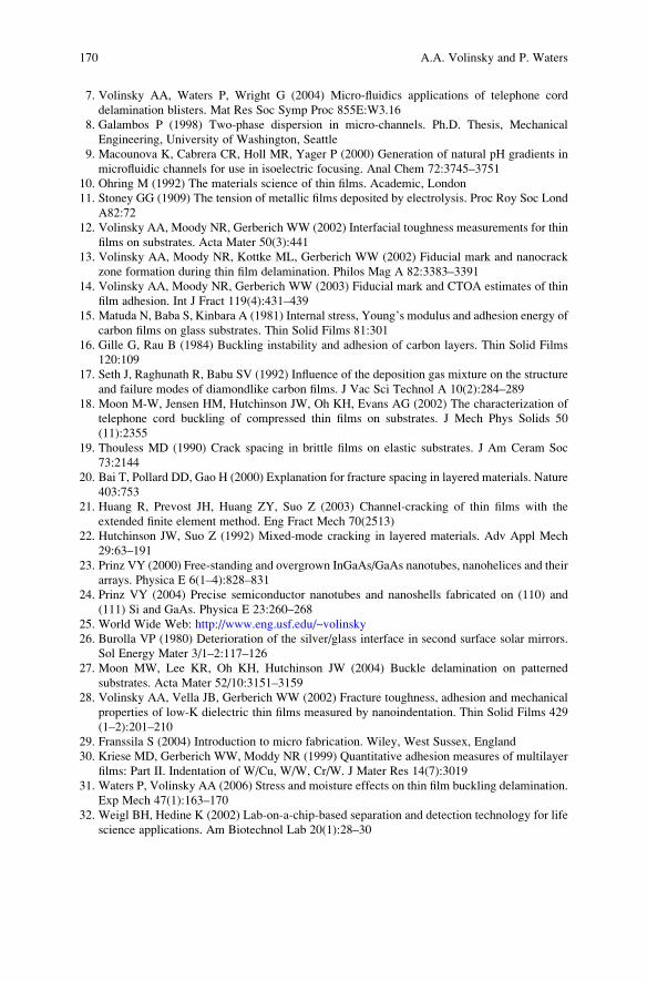
photoresist profiles, after testing a range of exposure times, can be seen in
Figs. 8.10 and 8.11. The photoresist width and thickness varied by up to 10%
across the 400 wafer diameter.
800
1000
1200
1400
1600
1800
2000
1000 3000 5000 7000
Thi
ckne
ss (
nm)
Spin Speed (rpm)
Fig. 8.9 Photoresist
thickness as a function of spin
speed for Shipley 1813
8 Delaminated Film Buckling Microchannels 163
0
0.5
1
1.5
0 50 100 150 200
10 sec8 sec6 sec4 sec
Hei
ght (
µm)
Width (µm)
Fig. 8.10 Photoresist profiles after different exposure times
Fig. 8.11 Effect of exposure time on the final photoresist thickness: (a) 10 s, (b) 8 s, (c) 6 s, and
(d) 4 s
164 A.A. Volinsky and P. Waters

At the shortest exposure time of 4 s, the remaining developed photoresist
measured 1.5 mm in height and 218 mm in width. However, on most of the wafer
there also remained a thinner layer of photoresist between the parallel lines. It was
concluded that an exposure time of 4 s at 275 W was inadequate. From there the
exposure time was increased by 2-s increments, with the final resist height and
width being inversely proportional to the exposure time. Along with decreasing line
height and width, the resist profile ended up being more rounded as the exposure
time was increased.
After exposure, the wafers were placed in a developer bath for 30 s and were then
rinsed with deionized water. Nitrogen was used to remove the majority of the excess
moisture on the wafer, which was then hard baked on a hot plate at 110 �C for 100 s.
Overall, the lithography techniques used here were adequate in accomplishing
the objective of creating simple patterns on a wafer. However, a more thorough
approach can be taken in the future for optimizing spin speed and time, bake time
and temperature, and exposure and development time. It must be understood that
the line widths created here are relatively large when compared with other lithog-
raphy techniques. Therefore, the quick optimization steps used here were adequate.
If smaller line widths and heights were required, a more meticulous approach would
be needed. The final step in the process was to deposit a tungsten film that is forced
to have compressive residual stress.
8.5 Buckling Delamination Morphology
The various shapes of buckled regions evolve in film/substrate systems that are in a
state of biaxial compression. Details of their shape and size will depend on factors
such as the film stress, thickness, and interfacial toughness. The buckling geometry
can be used to assess the interfacial toughness. Figure 8.12 is a picture of three
straight-sided delaminations of a tungsten and DLC film stack on a silicon wafer.
Fig. 8.12 Straight-sided
delaminations of a W/DLC
film on Si
8 Delaminated Film Buckling Microchannels 165

Assuming that fracture happens at the interface, (8.2) through (8.5) can be
applied to solve for the interfacial toughness between the photoresist and the
tungsten film, when straight-sided delaminations are present. One of the initial
deposition tests was on a silicon wafer patterned with the larger 200 mm wide
photoresist lines. The tungsten film was deposited for 50 min with an argon pressure
of 5 mTorr. This resulted in straight-sided delaminations forming across the width
of the photoresist line, as shown in Fig. 8.13a. The profile of the straight-sided
delamination widths is shown in Fig. 8.13b. Using the delamination height, d, thedelamination half width, b, and (8.2)–(8.5), the critical buckling stress was calcu-
lated to be 194 MPa. The residual stress of the film was found to be 313 MPa, the
steady-state interfacial toughness was found to be 0.0114 J/m2, and the mode-
dependent interfacial toughness was found to be 0.0859 J/m2.
The steps taken for calculating the interfacial toughness assumed that fracture
took place at the tungsten/photoresist interface. There is a possibility that the crack
propagates in the photoresist, at the interface between the photoresist and the silicon
substrate, or a combination of above mentioned. No matter where the crack is
propagating, however, the important thing is that the interfacial toughness between
the tungsten film and the silicon substrate, which has been reported in literature to
be 1.73 J/m2 [30], is stronger than that measured in the photoresist areas.
Moon et al. have found that the delamination morphology can be predicted when
the film stress is compared to the buckling stress [27]. For sr/sB < 6.5 straight-sided
delaminations are predicted and for sr/sB > 6.5 telephone cord delaminations are
predicted. For the delaminations shown in Fig. 8.13, sr/sB ¼ 1.6, which agrees with
the Moon et al. findings. Their predictions of delamination morphology were based
on similar experimental methods that utilized lithography techniques in applying
patterned areas of low interface adhesion surrounded by areas of high adhesion. By
controlling the width of the low-adhesion strips, the buckle morphology was
controlled.
Fig. 8.13 Tungsten delamination: (a) Optical image of delamination morphology and (b) Profile
of delaminations
166 A.A. Volinsky and P. Waters

Ideally the delaminations would propagate parallel to the photoresist lines as
opposed to perpendicular to them, as seen in Fig. 8.13. The main reason in preventing
this from happening is that the photoresist line is too wide. The photoresist is so wide
that it exceeds the critical buckling width, thereby allowing enough room for the
straight-sided delaminations to run perpendicular to the lines. Figure 8.14 shows two
different delamination morphologies that are possible when the photoresist line is
decreased in width. Telephone cord delamination morphology can be observed in
Fig. 8.14a when the photoresist width was approximately 120 mm. When the photo-
resist width was reduced to approximately 80 mm, as shown in Fig. 8.14b, a straight-
sided delamination was created. Unfortunately, as shown in Fig. 8.14b, tungsten
delamination also occurred in between the photoresist lines.
The delamination morphology that was observed in Fig. 8.14 would be neces-
sary if the delaminations were to find future use in transporting fluids. Continued
work is necessary to further experiment with photoresist width and its effect on
delamination morphology. Attention to deposition parameters, in regard to
controlling the residual stress, was found to be more important when using the
adhesion-reducing layers. Not only was delamination occurring in the patterned
areas, but it was also common to see the delamination propagate across other areas
of the wafer. The adhesion-reducing areas acted as crack initiation sites that helped
spawn delamination upon film deposition. There appears to be a fine line between
creating delaminations on the patterned areas and creating them on the rest of the
wafer. Controlling the exact amount of compressive residual stress is critical for
this method to succeed in the consistent creation of microchannels.
8.6 Conclusions and Outlook
By using photolithography to create adhesion-reducing layers, buckling
delaminations have been controlled and show potential use as microchannels.
Delamination morphology depends on two conditions: (1) the buckling stress
Fig. 8.14 Delamination morphology with different photoresist widths: (a) Telephone cord
delamination and (b) straight-sided delamination
8 Delaminated Film Buckling Microchannels 167

which is controlled by the adhesion-reducing layer’s width and (2) the amount of
compressive residual stress in the thin film. Here, telephone cord delaminations
were observed at larger photoresist widths and straight-sided delaminations were
observed for smaller photoresist widths. Line widths between 80 and 220 mm were
created.
By using standard lithography techniques, areas of low adhesion were created to
control delamination morphology. This could be used as a new method for creating
microchannels for transporting, mixing, and storing fluids in microfluidic devices.
Current methods for creating microchannels involve etching and wafer bonding.
The potential advantages of this new method are found in its ease of manufacturing
and its cost-effectiveness. Proof of concept was provided here by using a photore-
sist as the adhesion-reducing layer. By controlling the photoresist line width, the
delamination morphology was consequently controlled.
Microfluidics has been a rapidly growing field, along with the rest of the
microelectronics boom. In the late 1980s the early stages of microfluidics were
dominated by the development of microflow sensors, micropumps, and microvalves
[1]. Like many different areas of engineering, having everyone agree on a set
definition is sometimes difficult. Microfluidics does not differ in this regard. One
point that the majority can agree upon is that a microscopic quantity of fluid is the
key issue in microfluidics. One main advantage of microfluidics is utilizing scaling
laws for achieving better sensor performance. As the fluid volume is decreased,
there will also be a need to decrease the size of the channels the fluid is transported
in. Some possible delamination sizes created here are shown in Fig. 8.15. The
delamination channel width was varied from 25 to 60 mm and the height was varied
from 0.75 to 2 mm.
An interesting effect has been observed with the introduction of water at the film/
substrate interface of highly compressed films. Water appears to reduce interfacial
toughness, thereby allowing for the initiation of spontaneous delamination propa-
gation. Figure 8.16 shows the propagation of a telephone cord delamination, over a
0
0.5
1
1.5
2
0 10 20 30 40 50 60
W/SiW/Photoresist
Hei
ght (
µm)
Width (µm)
Fig. 8.15 Different
delamination channel profiles
168 A.A. Volinsky and P. Waters

90-s time interval, when water was introduced at the lower left-hand corner [31]. In
this case (Fig. 8.16), the delamination microchannels could be used as a one-time
use, disposable microfluidic device.
Using film delaminations to create microchannels shows promise in the field of
microfluidics. The key to creating the microchannels is in utilizing areas of reduced
adhesion to control the delamination morphology. Possible areas for future work
could be in finding better choices for adhesion-reducing layers and developing
more complex delamination patterns. Creating the microchannels is only a small
component of the overall picture if they are to be used in microfluidic devices.
Integration of the microchannels onto a “lab-on-a-chip”-type device [32] is the
overall goal, but many questions still need to be answered on how the fluid will be
placed into the microchannels and how the fluid will be transported once inside the
microchannels.
References
1. Nguyen NT,Werely ST (2002) Fundamentals and applications of microfluidics, Artech House,
Norwood, MA,1–19:285–286
2. Spence A, Retterer S, Isaacson M (2002) Microfabricated model silicon probes with
microfluidic, channels for drug delivery. NNUN Abstracts 2002/Biology & Chemistry, p 13
3. Li Y, Gulari MN, Wise KD (2003) High-yield buried microchannel formation for drug
delivery at the cellular level, In: Northrup MA, Jensen KF, Harrison DJ (eds) Proceedings of
mTAS 2003 seventh international conference on micro total analysis systems, vol 2, October
5–9, Squaw Valley, CA, pp 931–934
4. Volinsky AA (2003) Experiments with in-situ thin film phone cord delamination propagation.
Mat Res Soc Symp Proc 749:W10.7
5. Volinsky AA, Meyer DC, Leisegang T, Paufler P (2003) Fracture patterns in thin films and
multilayers. Mat Res Soc Symp Proc 795:U3.8
6. Volinsky AA, Waters P, Kiely JD, Johns EC (2005) Sub-critical telephone cord delamination
propagation and adhesion measurements. Mat Res Soc Symp Proc 854E:U9.5
Fig. 8.16 Delamination
propagation induced by the
introduction of water. Waters
and Volinsky [31], reprinted
with permission
8 Delaminated Film Buckling Microchannels 169
7. Volinsky AA, Waters P, Wright G (2004) Micro-fluidics applications of telephone cord
delamination blisters. Mat Res Soc Symp Proc 855E:W3.16
8. Galambos P (1998) Two-phase dispersion in micro-channels. Ph.D. Thesis, Mechanical
Engineering, University of Washington, Seattle
9. Macounova K, Cabrera CR, Holl MR, Yager P (2000) Generation of natural pH gradients in
microfluidic channels for use in isoelectric focusing. Anal Chem 72:3745–3751
10. Ohring M (1992) The materials science of thin films. Academic, London
11. Stoney GG (1909) The tension of metallic films deposited by electrolysis. Proc Roy Soc Lond
A82:72
12. Volinsky AA, Moody NR, Gerberich WW (2002) Interfacial toughness measurements for thin
films on substrates. Acta Mater 50(3):441
13. Volinsky AA, Moody NR, Kottke ML, Gerberich WW (2002) Fiducial mark and nanocrack
zone formation during thin film delamination. Philos Mag A 82:3383–3391
14. Volinsky AA, Moody NR, Gerberich WW (2003) Fiducial mark and CTOA estimates of thin
film adhesion. Int J Fract 119(4):431–439
15. Matuda N, Baba S, Kinbara A (1981) Internal stress, Young’s modulus and adhesion energy of
carbon films on glass substrates. Thin Solid Films 81:301
16. Gille G, Rau B (1984) Buckling instability and adhesion of carbon layers. Thin Solid Films
120:109
17. Seth J, Raghunath R, Babu SV (1992) Influence of the deposition gas mixture on the structure
and failure modes of diamondlike carbon films. J Vac Sci Technol A 10(2):284–289
18. Moon M-W, Jensen HM, Hutchinson JW, Oh KH, Evans AG (2002) The characterization of
telephone cord buckling of compressed thin films on substrates. J Mech Phys Solids 50
(11):2355
19. Thouless MD (1990) Crack spacing in brittle films on elastic substrates. J Am Ceram Soc
73:2144
20. Bai T, Pollard DD, Gao H (2000) Explanation for fracture spacing in layered materials. Nature
403:753
21. Huang R, Prevost JH, Huang ZY, Suo Z (2003) Channel-cracking of thin films with the
extended finite element method. Eng Fract Mech 70(2513)
22. Hutchinson JW, Suo Z (1992) Mixed-mode cracking in layered materials. Adv Appl Mech
29:63–191
23. Prinz VY (2000) Free-standing and overgrown InGaAs/GaAs nanotubes, nanohelices and their
arrays. Physica E 6(1–4):828–831
24. Prinz VY (2004) Precise semiconductor nanotubes and nanoshells fabricated on (110) and
(111) Si and GaAs. Physica E 23:260–268
25. World Wide Web: http://www.eng.usf.edu/~volinsky
26. Burolla VP (1980) Deterioration of the silver/glass interface in second surface solar mirrors.
Sol Energy Mater 3/1–2:117–126
27. Moon MW, Lee KR, Oh KH, Hutchinson JW (2004) Buckle delamination on patterned
substrates. Acta Mater 52/10:3151–3159
28. Volinsky AA, Vella JB, Gerberich WW (2002) Fracture toughness, adhesion and mechanical
properties of low-K dielectric thin films measured by nanoindentation. Thin Solid Films 429
(1–2):201–210
29. Franssila S (2004) Introduction to micro fabrication. Wiley, West Sussex, England
30. Kriese MD, Gerberich WW, Moddy NR (1999) Quantitative adhesion measures of multilayer
films: Part II. Indentation of W/Cu, W/W, Cr/W. J Mater Res 14(7):3019
31. Waters P, Volinsky AA (2006) Stress and moisture effects on thin film buckling delamination.
Exp Mech 47(1):163–170
32. Weigl BH, Hedine K (2002) Lab-on-a-chip-based separation and detection technology for life
science applications. Am Biotechnol Lab 20(1):28–30
170 A.A. Volinsky and P. Waters