chapter 6 finalthesis.library.caltech.edu › 1916 › 9 › boonratchapter6.pdf1. thermoplastic...
TRANSCRIPT

VI-1
CHAPTER VI Novel Methods for Joining Materials Using Metallic Glasses – an
Alternative to Lead-Free Soldering
Abstract
Since the European Union enacted Restriction of Hazardous Substances directive
(RoHS), the semiconductor and electronic industries have been under a lot of pressure to
phase out lead solder and to find a reliable Pb-free solder alternative. Currently, there
are many reliability issues associated with the current Pb-free solder technology based
on tin and silver. To date a “drop-in” substitute to lead solder has not been found.
We introduce novel methods for metal-to-metal or material-to-material joining
which rely on the superior mechanical properties of bulk metallic glasses and/or their
softening behavior in the undercooled liquid region. The method, for example, enables
lead-free soldering to the semiconductor industry and allows the aircraft industry to join
two pieces of metal together at much lower temperatures than the typical ranges used for
brazing or welding.
Gold-based and platinum-based are the current BMGs of choice used in the
experiments because of their low glass transition temperatures comparable to the reflow
temperatures of the soldering process.

VI-2
1. Background
1.1 The Urge for a New Technology
Health and environmental issues related to Pb (lead) have been documented over
many decades. Lead poisoning is a serious health threat which usually occurs after a
prolong exposure to lead and lead compounds. Nonetheless, lead can still be found in
many consumer products, including storage batteries, ammunitions, and electronic
products. While storage batteries account for approximately 80% [1] of lead
consumption, its recycling program is very effective and therefore posts no health
concerns. Solder usage in electronic materials is of particular concern because of the
contamination in landfills where the products are discarded. Lead solder on discarded
circuit boards contaminates the soil and leaches into the ground water system.
Many countries around the world have taken preemptive steps to prevent lead-
related health problems over the past two decades. One of the most authoritative
milestones came from the European Union (EU) who enacted the Restriction of
Hazardous Substances (RoHS) directive to completely phase out lead from many
electronic products.
Many countries have followed suit since RoHS adoption in 2003. As of July 1st,
2006, lead and a few other hazardous substances were banned from most consumer
electronic products. Many governments in Asia including China, Korea, and Japan have
come up with their own version of RoHS. In the US, California’s SB20 has prohibited the

VI-3
sale of electronic devices which contain any substances prohibited by the EU’s ROHS
since January 1st, 2007.
There has been ongoing research effort [2-4] to find a substitute for Pb solder for
more than a decade but no clear solution has been found. The present industry solder
standard includes a few varieties of near-ternary eutectic alloy of tin (Sn), silver (Ag),
and/or copper (Cu) alloys (SAC solder) with possible minute additions of “performance-
enhancing” elements such as bismuth (Bi) [5], indium (In) [6], zinc (Zn) [7], and
antimony (Sb).
1.2 Problems of Current Lead-Free Solder Technology
1.2.1 Higher Temperature Requirement
The current SAC solders containing a few percent of Ag and Cu melt between
217 – 225 oC. The melting temperatures are more than 30 oC above that of Pb-Sn based
solder which has a eutectic at ~183 oC. The higher processing temperature requirement
creates complications in any product line containing multiple soldering processes, e.g.,
flip-chip packaging, where the temperature of the last reflow process dictates the
temperature of prior reflow processes. The industry must now use solders that melt from
215 ˚C to as high as 250 ˚C to avoid the remelting of solder in the preceded reflow steps.
From the chip-manufacturing stand point, such high packaging temperature also calls for
a total redesign of the chip architecture which may not be cost effective.

VI-4
1.2.2 Wetting, Spreading, and Bonding
Molten lead has a very low surface tension – the characteristic that contributes to
lead’s excellent wettability and spreading. The wetting characteristic of Pb/Sn solder far
exceeds those of lead-free alternatives. At the interconnect interface, Pb/Sn solder forms
chemical bond by creating stable pure Sn crystalline phase. The SAC solders would
contain at least three competing phases: β-Sn, Ag3Sn [8], and Cu6Sn5 [9]. The latter two
are non-equilibrium intermetallic compounds which nucleate and grow with minimal
undercooling [10]. Adequate undercooling usually translates to the reduction of residual
differential thermal stresses. The lack of undercooling and the existence of intermetallic
compounds raises some reliability concerns discussed in the next section.
1.2.3 Thermal, Mechanical, and Electrical Reliability
Mechanical attachment, electrical conduction, and thermal pathway are the three
main functions of solder joints, particularly in flip-chip industry. Mechanical-related
problems usually stem from the mismatch of the coefficients of thermal expansion
between the materials attached to both ends of the solder joints, as well as the mismatch
between the solder joint and attached substrate materials. During thermal cycling, the
ousted Pb-solder joints release thermally induced stresses by plastic deformation [11];
such process is not possible with SAC solder. Current solder joints typically fail under
moderate temperature cycling. Another shortcoming of SAC solder is electromigration
[12], especially where the joints are operated at high current density [13]. Figure VI-1

VI-5
and Figure VI-2 show two common failures of solder joints (SEM micrographs courtesy
of Dr. Daewoong SuhA of Intel Corporation).
Figure VI-1: Solder thermal-mechanical fatigue failure during temperature cycling
Figure VI-2: Solder electromigration failure during operation
A Collaborative interactions and project reporting are carried out with Dr. Suh as the Intel point of contact.
e-

VI-6
2. Bulk Metallic Glass as Solder Joints
BMGs may be processed like thermoplastics when the materials are heated above
the glass transition temperature, Tg. By matching this “softening” temperature of BMGs
(10-60 K above Tg) to the actual soldering process temperature, different BMGs could be
chosen as low temperature replacements for Pb-Sn and Sn-based solders. Additionally,
BMGs may be used as reliable lead-free solders by deep undercooling directly from the
melt. In summary, BMGs could be utilized as solders in at least two different techniques:
1. Thermoplastic processing for soldering (method (1) as shown in Figure VI-3)
1.1 Thermoplastic soldering relying on BMG-substrate intimate contacts
1.2 Thermoplastic soldering relying on mechanical interlocking
2. Deeply undercooling process from molten liquid
2.1 Amorphous or glassy solder joint (method (2.1) as shown in Figure VI-3)
2.2 Controlled crystalline microstructure in solder joint using undercooled
metallic glass former liquid (method (2.2) as shown in Figure VI-3)

VI-7
Figure VI-3: Schematic showing possible BMGs processing pathways as solder. The
shaded region represents the solid phase. Both crystalline and supercooled
liquid occupy the upper portion of the diagram.
It is important to note that processing pathways (2.1) and (2.2) require the solder
material to be completely molten at approximately 250 ºC for the alternative Pb-free
solder process. If we assume Turnbull’s parameter Trg>0.6 for good glass forming ability
(GFA), the Tg of such BMG is of the order of 40-50 ºC which implies that the solder
joint will not be stable under operating conditions. However, the deep undercooling
characteristic alone should suffice for stress minimization because the volume shrinkage
is greatly reduced. Therefore, for the sub-250 ºC soldering purpose, it is not relevant if
the solder joints are initially fully amorphous or partially amorphous or completely

VI-8
crystalline. In fact, a hypoeutectic composition of Au-, Pt-, or Sn-based systems is
preferred so that a ductile dendritic phase is expected as the primary solidification.
The stress mitigation strategy can be summed up in Figure VI-4 which shows the
relationship between volume and temperature during cooling from the molten state. A
conventional solder cooling from the melt will follow Path A in Figure VI-4. There is a
dramatic drop in volume (ΔV ~3-8%) when the liquids solidify and atoms efficiently
rearrange themselves into crystal lattices. This volume shrinkage contributes to residual
thermal stress in the solder joint. In an amorphous alloy, however, negligible volume
change associated with vitrification is expected. The effect translates into less thermal
stress stored in the solder joints. Following Path B in Figure VI-4, the alloy can
undercool and solidify with less solidification shrinkage. Path C in Figure VI-4
demonstrates the way an alloy can ultimately be frozen into a non-crystalline amorphous
state.
The focus of this chapter will be devoted to the discussion of processing pathway
(1), as shown in Figure VI-3.

VI-9
Figure VI-4: Volume and temperature diagram of a solder cooling process. Path A
represents the conventional solder alloy with minimal undercooling. The
alloy solidifies in the crystalline state near or at the melting temperature
and undergoes substantial shrinkage. The alloy in Path B exhibits sizeable
undercooling which translates to small solidification shrinkage. Path C
shows the situation where the undercooling and cooling rate are sufficient
to bypass the crystallization event completely.

VI-10
3. Experimental Setup
Samples were prepared by alloying the elements (Au: 99.99%, Pt: 99.99%, Cu:
99.9%, Ni: 99.9%, Ag: 99.9%, Pd: 99.95%, Si: 99.95%, P: 99.5% purity) in an arc-
melter. Copper mold quenching was performed to vitrify the alloy in its amorphous state.
The fully amorphous cast strips are cut into smaller “feedstock” pieces as shown in
Figure VI-5. Feedstock of certain shapes (e.g., spherical (Figure VI-6)), must be remelted
in an arc-melter, tower-dropped under gravity, or squirted into liquid using a jet-nozzle.
Figure VI-5: Cuboid-shape solder is placed on copper slug substrate with flux applied as
a cleaning agent.

VI-11
Figure VI-6: Solder balls of 1 mm diameter can be obtained by remelting the alloy in an
arc-melter.
A glassy solder (feedstock material) is positioned in between two high purity
copper slugs as shown in Figure VI-7 with an optional flux applied. The assembly stack
is inserted into Perkin Elmer Thermal Mechanical Analyzer (TMA7) to be heated to a
temperature above glass transition temperature deep into the supercooled liquid region.
The solder can be held in the amorphous (supercooled liquid) state for anywhere from a
few minutes up to several hours. Heating may be accompanied by compressive loading to
facilitate the spreading of the supercooled liquid solder.
Processing conditions depend on different alloy families and composition. For
example, processing temperatures were investigated at 20-60 ˚C above Tg for gold BMG
and 30-75 ºC above Tg for platinum BMG. Our investigated Au-BMG alloy has Tg at
130 ˚C [14] which means the thermoplastic soldering test should be conducted at 160 –

VI-12
190 ˚C. The temperature window is significantly below the 210-230 ˚C processing
temperature window for conventional Sn-based solder.
Figure VI-7: Copper-solder-copper stack is loaded into Perkin Elmer TMA7 for accurate
control of temperature and load during thermoplastic soldering.
Three-point bending experiments were conducted to obtain valuable viscosity
information for both the Pt-BMG and Au-BMG currently investigated. Combined with
prior crystallization and TTT diagram studies, figures of merit could be obtained to
quantitatively predict the solderability of our BMGs with respect to processing
temperature and time.
VI-13
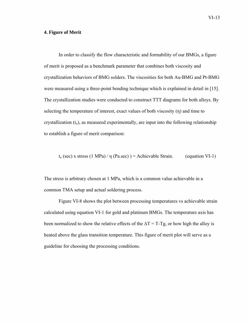
4. Figure of Merit
In order to classify the flow characteristic and formability of our BMGs, a figure
of merit is proposed as a benchmark parameter that combines both viscosity and
crystallization behaviors of BMG solders. The viscosities for both Au-BMG and Pt-BMG
were measured using a three-point bending technique which is explained in detail in [15].
The crystallization studies were conducted to construct TTT diagrams for both alloys. By
selecting the temperature of interest, exact values of both viscosity (η) and time to
crystallization (tx), as measured experimentally, are input into the following relationship
to establish a figure of merit comparison:
tx (sec) x stress (1 MPa) / η (Pa.sec) ) = Achievable Strain. (equation VI-1)
The stress is arbitrary chosen at 1 MPa, which is a common value achievable in a
common TMA setup and actual soldering process.
Figure VI-8 shows the plot between processing temperatures vs achievable strain
calculated using equation VI-1 for gold and platinum BMGs. The temperature axis has
been normalized to show the relative effects of the ΔT = T-Tg, or how high the alloy is
heated above the glass transition temperature. This figure of merit plot will serve as a
guideline for choosing the processing conditions.

VI-14
10 15 20 25 30 35 40 45
0
5
10
15
20
25
30
35 Pt-BMG Au-BMG Pt's Figure of Merit (Linear Fit) Au's Figure of Merit (Linear Fit)
Ach
ieva
ble
Stra
in
T - Tg
Figure VI-8: Figures of merit are shown for Pt-BMG and Au-BMG. The achievable
strain for each temperature is calculated using experimental values for both
viscosity and time to crystallization (see equation VI-1).
VI-15
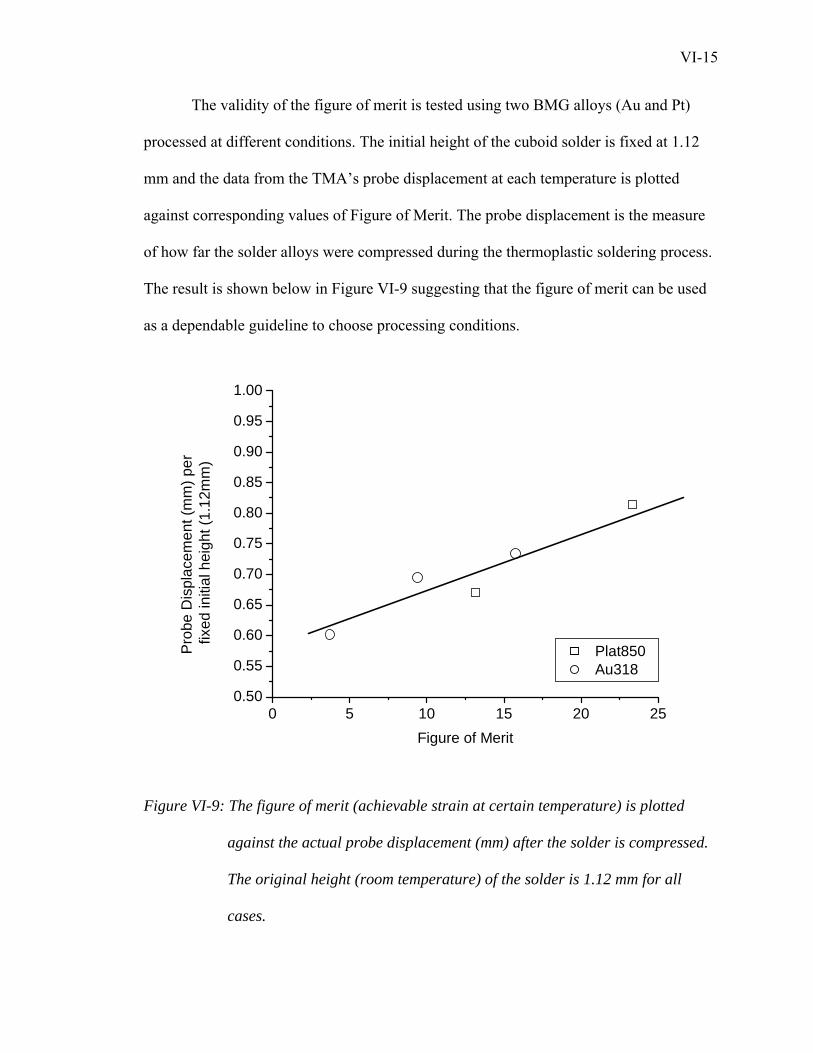
The validity of the figure of merit is tested using two BMG alloys (Au and Pt)
processed at different conditions. The initial height of the cuboid solder is fixed at 1.12
mm and the data from the TMA’s probe displacement at each temperature is plotted
against corresponding values of Figure of Merit. The probe displacement is the measure
of how far the solder alloys were compressed during the thermoplastic soldering process.
The result is shown below in Figure VI-9 suggesting that the figure of merit can be used
as a dependable guideline to choose processing conditions.
0 5 10 15 20 250.50
0.55
0.60
0.65
0.70
0.75
0.80
0.85
0.90
0.95
1.00
Pro
be D
ispl
acem
ent (
mm
) per
fix
ed in
itial
hei
ght (
1.12
mm
)
Figure of Merit
Plat850 Au318
Figure VI-9: The figure of merit (achievable strain at certain temperature) is plotted
against the actual probe displacement (mm) after the solder is compressed.
The original height (room temperature) of the solder is 1.12 mm for all
cases.

VI-16
5. Experimental Results of Flat-Surface Soldering
Various processing conditions were tested to optimize the thermoplastic
processing parameters. The results are compared using tensile test to measure the
debonding strength of the solder joints. Both surfaces of the debonded joint (copper slug
surface and reflowed solder surface) are examined using a scanning electron microscope
(SEM) to understand the flow characteristic and effect of different surface treatments.
Some samples were cross-sectioned to study the condition of the interface between solder
and substrate.
5.1 Solder Materials
Au-BMG (Au49Ag5.5Pd2.3Cu26.9Si16.3), Pt-BMG (Pt57.5Cu14.7Ni5.3P22.5), and a Zr-
Cu-Be based alloy were investigated. The first two alloys are precious-metal based and
are known for their inertness to oxidation. Gold alloys particularly have low Tg at 130 ºC,
which allows the thermoplastic soldering process to be performed at 170-200 ºC which is
the temperature range preferred by the electronic industry. Pt-BMG was chosen because
of its superior performance to gold (as predicted by figure of merit) and its processing
temperature range between 230-290 ºC. The Zr-based alloy is chosen because of its
exceptionally large supercooled liquid region which allows the alloy to be processed at an
elevated temperature of at least 100 ºC above Tg, resulting in very low viscosity.
Our findings concur with the figure of merit prediction that Au-BMG solders did
not work when compared to Pt-BMG solders. The debonding strength of all Au-BMG

VI-17
solders (processed at various conditions) did not exceed the 1 MPa mark while Pt-BMG
solders exhibit as high as a 8-10 MPa debonding strength. The Zr-BMG, by contrast, had
serious oxidation problems at high processing temperature (above 400 ºC) and virtually
all experiments failed.
5.2 Processing Temperatures
According to a figure of merit plot, the higher temperature signifies higher
achievable strain. Our experiments also confirm the initial prediction that the probe
travels further (larger strain) at higher probe velocity when temperature is high. The
higher temperature also translates to the higher resulting debonding strength. However
the upper limit of processing temperature is controlled by another factor, and that is the
time allowed for the solder to be reflowed in an actual experiment.
If the temperature is high, the time to crystallization is short and that means the
experiment should be completed very quickly before the crystallization takes place.
If the temperature is too high, the experimental time is not enough to complete the
reflow process before the solder crystallizes prematurely, and therefore it will not spread
out far enough to establish adequate contact surface area.
The best processing temperature for Pt-BMG is found to be in 280-295 ºC range,
but the results also greatly depend on other factors as well. The Au-BMG works best at
around 170-185 ºC.

VI-18
5.3 Shape of Feedstock Solder
We discovered that the reflowed surface condition greatly affects the debonding
strength of our joints. Trapped air pockets are the common feature found in most joint
surfaces that fail prematurely. Vice versa, the surface of the solder joint that could sustain
higher debonding strength is smooth and has minimal air pockets. Figure VI-10 shows
the surface of reflowed solder that was originally of cuboid shape. The original rectangle
“base” could still be seen as a faint outline in the top picture. Further examination reveals
that the trapped air pockets are concentrated around the inside of the rectangular base
outline, as shown in the bottom picture. The finding suggests that in order to achieve
good bonding surface, the creation of new surfaces is preferred. After a few shape-
optimization investigations, the most current solder shape design calls for a perfect
spherical shape that is smaller in size. Such a solder feedstock shape could be made using
drop-tower, jet-nozzle, water quenching, or melting in high viscosity fluxing agent (e.g.
Boron-oxide).

VI-19
Figure VI-10: Top image shows the top view of the debonded solder joint surface sitting
on copper slug. The original feedstock solder is in cuboid shape
(rectangular base outline can still be seen in both images). Many air
pockets are found trapped on the inside of the rectangular base of the
original solder, suggesting that the creation of new surface is crucial to
make intimate contact.

VI-20
5.4 Surface Treatment
Different surface treatment conditions were tested to pinpoint the best surface for
thermoplastic processing processes. The surface conditions investigated include:
- as-received surface with fluxing agent
- as-received surface with no fluxing agent
- polished surface with fluxing agent
- polished surface with no fluxing agent
- rough (sanded) surface with fluxing agent
- rough (sanded) surface with no fluxing agent
- acid-dipped surface with no fluxing agent
- gold-sputtered surface
We have concluded that the fluxing agent is a double-edged sword – flux helps
with the cleansing of copper oxide layers on the copper substrate surface. However, the
flux residue left behind could act as voids and crack-propagation sites. We have also
confirmed that, without melting, intimate contact between solder and substrate is
possible, as shown in Figure VI-11. This is not a surprising result because it has been
known that solid state amorphization is possible at temperatures near Tg [16].
In summary, the acid-dipped surface (no fluxing agent) is found to be the best
surface treatment for Pt-BMG solder on copper substrate. In one particular case, copper
residue is found attached on the solder surface after the debonding test. The tearing of
copper substrate indicates that the debonding strength could locally exceed the flow stress

VI-21
of high purity copper. This is in complete opposition to all SAC solder joints, where the
failure always occurs at the solder, not at the copper substrate.
Figure VI-11: Intimate contact is demonstrated between Pt-BMG solder (top) and copper
substrate (bottom) (cross section).

VI-22
Figure VI-12: Top left picture shows Backscattered SEM image of Pt-solder, which is
embedded with many small copper pullouts (top view). Top right picture is
the magnified image of the large copper piece. Bottom pictures are SEM
images from a different sample showing some copper pieces that got
pulled out during the debonding test. The composition of all the dark
areas is confirmed to be pure copper using EDS analysis.

VI-23
5.5 Crystallization Effect
It should be noted that there are primary two crystallization processes involved in
thermoplastic soldering:
(i) The crystallization process which happens during the early reflow process
must be avoided. This includes the crystallization that might occur during feedstock
production process. These crystallites impede with the solder reflowing process, resulting
in limited expansion of the solder. In some extreme cases, the solder balls collapse
catastrophically if the compressive load is too high and the solder could not flow fast
enough to accommodate loading stress.
(ii) The crystallization process that occurs towards the end of the reflow process
(or after the process is finished) has no detectable effect on the debonding strength of
solder joints. In many cases, we find small crystallites on the solder surface, but their
surface features replicate that of the copper surface. This suggests that the solder flowed
onto copper surface first in its supercooled liquid state and replicated the Cu surface
feature, and then the crystallites formed after the reflow is completed.
5.6 Compressive Load and Flat-Surface Soldering Summary
High compressive load offers constructive effect to the thermoplastic soldering
process. However, the load has been limited to about 5 N to reflect the level that is easily
achievable in manufacturing processes. Using optimized soldering conditions, the joint is
exhibiting approximately 5-10 MPa debonding strength, which is only 10-20% of the
ultimate tensile strength of a SAC solder bond. Careful investigation reveals that the

VI-24
solder surface never comes in full contact around the outer edge of the reflowed solder.
This is the result of the flow behavior of the free-moving solder front. The viscous solder
front is moving in parallel to the copper substrate. As shown in Figure VI-13, when the
fresh new solder surface first comes in contact with the substrate (point A) and there is no
normal force contribution that “presses” the fresh solder material against the substrate.
The pressure only builds up after the flow front moves further outwards. Figure VI-14
shows a cross section of the solder near the flow front. There is an apparent gap between
the solder and the substrate.
Figure VI-13: At point A near the free flowing front, there is negligible normal force
contribution that presses the fresh solder material against the substrate.
The normal pressure only builds up after the front has moved forward.
BMG solder
Copper Substrate
Copper Substrate
A A

VI-25
Figure VI-14: Cross section of solder-substrate interface is shown. The interface near the
free flowing front does not have enough normal force to press the material
against the substrate. The solder material does not come in full contact to
the substrate in the area shown inside the ellipse.

VI-26
Figure VI-15: The top view of the solder surface shows less than 100% contact area with
the substrate, as outlined by the solid line. This can be confirmed by the
replicated surface features found on the flowed surface of the solder. Only
inside the boundary (to the right) shows that the surface of copper is
replicated to the reflowed solder.

VI-27
6. Modifying the Pressure Distribution
Figure VI-16: Special copper slugs were prepared by drilling 500-micron holes
perpendicular to the surface.
Shown in Figure VI-16, 500 micron holes were drilled perpendicularly into the
copper slug surface in a five-by-five pattern. The soldering reflow process was conducted
using these special slugs installed on both sides of the solder (top and bottom). The
resulting reflowed solder is shown in Figure VI-17. The cylinders’ height profile suggests
a drop in pressure as the solder is flowing towards the outer edge. Such an analog
pressure profile is crucial in determining new substrate design to increase the normal
pressure, especially towards the outside of the solder.

VI-28
Figure VI-17: Analog pressure profile of solder during the reflow process. The drop in
pressure agrees with prior suspicion that near the free flowing solder
front, the normal force needed to press solder material against substrate is
small. The new substrate design is required to improve the intimate
contact around the outer edge of reflowed solder.
New substrate designs that encourage higher normal pressure to press the material
against the substrate include:
1. Limiting the free-flowing solder front. An aluminum sleeve has been slip-fitted
around the copper slugs. Once the material flows to the edge during the reflow process,
the aluminum sleeve restricts the further flowing of the solder front and therefore creates

VI-29
more normal force. Our preliminary result has already shown noticeable improvement
over the free-flowing front process.
2. Introducing angled substrate. By introducing a 45º slant angle to the substrate,
we are hoping to de-couple the free flowing surface to contribute equal normal forces on
top and bottom substrate. The concept is shown in Figure VI-18. The soldering result
from this angled-surface copper substrate design is not yet available at the present time.
Figure VI-18: By introducing slanted surface(left) or restricting-block (right) substrate,
the solder front is no longer free flowing. For the slanted surface case,
our calculation shows that, if the slanted angle is 45º, there should be two
equal normal pressures that “press” the material against the substrate
during reflow.

VI-30
7. Mechanical Interlocking
Another approach to improve better bonding is to introduce an actual interlocking
mechanism. By comparing the yield strengths of copper substrate (yield strength of 70
MPa and ultimate tensile strength of 220 MPa) and Pt-BMG (yield strength of 1400
GPa), we could assume that the failure would likely occur at the copper substrate.
Therefore, by joining the two materials together using an interlocking mechanism inside
the copper substrate, the debonding strength could be as high as what the copper substrate
could sustain. The ultimate tensile strength of the solder joint depends greatly on the
design of the locking mechanism on the substrate side.
To test the idea, a new copper substrate design is being developed to utilize the
mechanical interlocking concept, as shown in Figure VI-19. While the actual substrates
are being fabricated, we use SolidWorks and COSMOSWorks to analyze the theoretical
strength of our interlocked joint. The result is calculated using 4x4 pattern (a total of 16)
of recessed-neck design similar to that shown in Figure VI-19. The material tested is
assumed to be linear elastic isotropic pure copper.
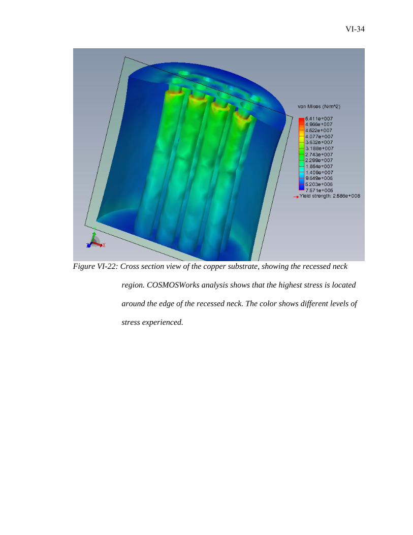
Our analysis shows the upper limit of debonding strength should be as high as
~259 MPa, more than a 500% increase over that of SAC solder. The side view, top view,
and cross-section view are shown in Figures VI-20, VI-21, and VI-22, respectively. The
COSMOSWorks simulation also indicates that the neck area is the weakest point, where
the material will fail first. This emphasizes the importance of the refilling process of the
material during the reflow.
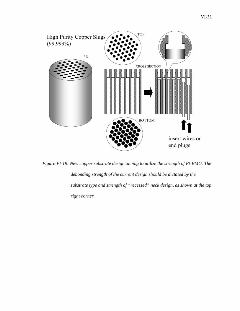
VI-31
High Purity Copper Slugs(99.999%)
insert wires or end plugs
TOP
CROSS SECTION
BOTTOM
3D
Figure VI-19: New copper substrate design aiming to utilize the strength of Pt-BMG. The
debonding strength of the current design should be dictated by the
substrate type and strength of “recessed” neck design, as shown at the top
right corner.

VI-32
Figure VI-20: Front section of the COSMOSWorks analysis showing the deformed
copper substrate before fracture. The calculated yield strength at 259
MPa can be treated as the upper limit of our debonding strength using Pt-
BMG on Cu substrate.

VI-33
Figure VI-21: Top view of the copper substrate. COSMOSWorks analysis shows the
stress experienced by different areas of the copper substrate right before
fracture. The color shows different levels of stress.
VI-34
Figure VI-22: Cross section view of the copper substrate, showing the recessed neck
region. COSMOSWorks analysis shows that the highest stress is located
around the edge of the recessed neck. The color shows different levels of
stress experienced.

VI-35
8. Summary
A thermoplastic soldering technique has been demonstrated. There are two
primary controllable processing parameters: (i) materials preparation and (ii) processing
conditions. The summary of experimented conditions is shown in the diagram illustrated
in figure VI-23 and VI-24.
A major advantage of our technique is because the processing temperatures can be
chosen based on the BMG alloy compositions and the glass transition temperature. The
method, for instance, permits metal-to-metal joining process at temperatures as low as
130-170 ºC which is the supercooled liquid region for Au-BMG. Gold and platinum
BMGs are the current tested materials because of their oxygen inert characteristic and
their low Tgs values.
The thermoplastic soldering process is carried at 20-60 ºC above Tg, which means
any BMG could be chosen as long as the processing temperature is within the
supercooled liquid region and the processing time is long enough for alloy complete
bonding before crystallization occurs and/or before the flow is arrested.
Flat surface soldering exhibits at least 6 MPa debonding strength while
mechanical interlocking could easily exceed 47 MPa debonding strength in our
preliminary results as shown in Figure VI-25. The maximum debonding strength may be
as high as 260 MPa, according to our SolidWorks Simulation.

VI-36
Figure VI-23: A summary of experimented materials preparation techniques are shown
in the diagram. Three main components that can be controlled are solder,
flux, and substrate.
Materials Preparation
Flux
Solder BMG Families
Feedstock Shapes
e.g. Au, Pt, Zr, Mg
e.g. BBs, balls
Substrates
Fluxes / Agents
No Flux
Different T Ranges
Material Choice
Surface Treatment
e.g. Cu, Ni, Ti
Au-Sputtered
Polished / Rough
Acid Etched
Surface Feature Mechanical Interlock
Flow Restriction

VI-37
Figure VI-24: A summary of experimented processing techniques are shown in the
diagram. Three main variables that can be controlled are processing
temperature, load, and soldering time.
and substrate.
Processing
Load
Temperature Isothermal
With Profiles
e.g. Tg + X oC
e.g. Activate Flux
Soldering Time
Constant Load
No Load
e.g. 1,5,8 N (<1 MPa)
Probe Movement
Until Crystallizes
e.g. Solder runs out
Probe Velocity
Pre-determined “Figure of Merit”
TTT Diagram / Nose
Viscosity

VI-38
0.0 0.1 0.2 0.3 0.4 0.5 0.6 0.7 0.8 0.9 1.00
2
4
6
8
10
12
14
16
18
20
22
24
0.0
4.3
8.7
13.0
17.3
21.7
26.0
30.3
34.7
39.0
43.3
47.7
52.0
Deb
ondi
ng S
treng
th (M
Pa)
p
roje
cted
are
a ~
4.5
mm
2
Load
(kgf
)
Extension (mm)
Debonding Strength (uniaxial tension)
Figure VI-25: Debonding strength in tension of a thermoplastically formed solder joint
which is comparable to the 40-50 MPa tensile strength of conventional
SAC solders. This particular experiment was done using Pt-BMG flowed
in a constrained substrate (right picture of Figure VI-18).

VI-39
References
[1] Lead and the Electronic Industry : A Proactive Approach, in: National Center for
Manufacturing Sciences, 1995.
[2] L. C. Prasad, Y. Xie, A. Mikula, Journal of Non-Crystalline Solids 250 (1999) 316-
320.
[3] J. W. Jang, P. G. Kim, K. N. Tu, M. Lee, Journal of Materials Research 14 (1999)
3895-3900.
[4] E. P. Wood, K. L. Nimmo, Journal of Electronic Materials 23 (1994) 709-713.
[5] Y. Kariya, M. Otsuka, Journal of Electronic Materials 27 (1998) 1229-1235.
[6] T. M. Korhonen, J. K. Kivilahti, Journal of Electronic Materials 27 (1998) 149-158.
[7] K. L. Lin, T. P. Liu, Materials Chemistry and Physics 56 (1998) 171-176.
[8] D. W. Henderson, T. Gosselin, A. Sarkhel, S. K. Kang, W. K. Choi, D. Y. Shih, C.
Goldsmith, K. J. Puttlitz, Journal of Materials Research 17 (2002) 2775-2778.
[9] X. Deng, G. Piotrowski, J. J. Williams, N. Chawla, Journal of Electronic Materials 32
(2003) 1403-1413.
[10] S. T. Kao, Y. C. Lin, J. G. Duh, Journal of Electronic Materials 35 (2006) 486-493.
[11] I. H. Kim, T. S. Park, S. Y. Yang, S. B. Lee, Advances in Fracture and Strength, Pts
1- 4 297-300 (2005) 831-836.
[12] F. Ren, J. W. Nah, K. N. Tu, B. S. Xiong, L. H. Xu, J. H. L. Pang, Applied Physics
Letters 89 (2006) -.
[13] L. H. Xu, J. H. L. Pang, F. Ren, K. N. Tu, Journal of Electronic Materials 35 (2006)
2116-2125.

VI-40
[14] J. Schroers, B. Lohwongwatana, W. L. Johnson, A. Peker, Applied Physics Letters
87 (2005) -.
[15] E. Bakke, Viscosity Measurements of Bulk Metallic Glass Forming Alloys, in: vol
Pd.D., California Institute of Technology, Pasadena, CA, 1997.
[16] R. Busch, E. Bakke, W. L. Johnson, Metastable, Mechanically Alloyed and
Nanocrystalline Materials, Pts 1 and 2 225 (1996) 141-146.