chapter 4 electronics 1. cathode ray oscilloscope (cro) · the cro can be divided into three main...
TRANSCRIPT

Awesome Physics with Alina Iman Arif@MRSM TGB
CHAPTER 4 ELECTRONICS
1.
CATHODE RAY OSCILLOSCOPE (CRO)
Diagram 1
Common function of CRO:
(a) To measure the potential difference (b) To measure the short time intervals (c) To display waveform
The physics concept applied by the CRO is called thermionic emission.
(a) What is meant by thermionic emission? Thermionic emission is the process of releasing electrons from a heated cathode surface.
(b) State the factors which can increase the rate of electrons released by the cathode? Bigger surface area of cathode is used Increase the temperature to the cathode Type of material to make cathode (cathode coated oxide can release more electrons)
(c) What is meant by cathode ray? Cathode ray is a fast moving electron beam from cathode to anode in a fine line.
(d) Why the CRO needed to be evacuated? To prevent the electrons from ionising the air molecules and collide with them. This may cause an irregular image on the screen.
(e) The fluorescent screen on CRO is coated with fluorescent material like phosphor. - State the function of the phosphor.
The function of phosphor is to convert the kinetic energy of electron into light energy. - Why the coating of screen is necessary?
Because the electrons beam is invisible. (f) How can the deflection of electrons be increased?
By increasing the potential difference

Awesome Physics with Alina Iman Arif@MRSM TGB
2.
The CRO can be divided into three main parts:
(a) Electron gun (Cathode, filament, control grid, focusing anode, accelerating anode) (b) Deflection system (x-plate, y-plate) (c) Fluorescent screen
Component Function
Filament To heat up the cathode Cathode To release electron
Control grid To control the number of electron to the screen and thus control the brightness of screen
Focusing anode To focus the electron to the screen and thus control the sharpness of image at screen
Accelerating anode To accelerate the electron to the screen x-plate To control the electron from deflecting to left or right y-plate To control the electron from deflecting up or down
Fluorescent screen To convert the kinetic energy of electron to light energy
Front view of CRO
Diagram 2
Control grid (intensity) ® control the brightness of screen Focusing anode (focus) ® control the sharpness of image on screen Y part (potential difference) ® showing the value of potential difference Position (Y-plate) ® to shift up or down the waveform Volts/Div ® to set the scale for y-axis which is voltage X part (sweep range) ® showing the time Position (X-plate) ® to move the waveform to the left or right Time/Div ® to set the scale for x-axis which is time Sweep range ® to turn on or off the time.

Awesome Physics with Alina Iman Arif@MRSM TGB
3. Graph and calculation involving CRO Waveform by CRO
y-input Time base is off Time base is on
No input
Dry cell (d.c current)
a.c power supply (from voltage
regulator)
EXAMPLE: Diagram 3 shows a trace on an oscilloscope for an a.c. source. The y-gain is set to 1.5 V cm-1 and the time base is 2 ms cm-1.
Diagram 3
(a)
Calculate the Vp, Vpp and Vrms.
Peak voltage Vp
Peak-to-peak voltage Vpp
Root mean square voltage Vrms
Vp = 1.5Vcm-1 × 2divs = 3.0 V
Vpp = 1.5Vcm-1 × 4divs = 6.0 V
Vrms = !"√$
= %.'√$
= 2.12 V

Awesome Physics with Alina Iman Arif@MRSM TGB
(b) Calculate the time taken for one waveform. Time for one wave, T = 2 ms cm-1 × 4 divs = 8 ms = 8 × 10⁻³ s
(c) Calculate the frequency, f of the a.c source. Frequency, f = (
) = (
(+×('-.)
= 125 Hz
(d) Sketch the trace that will be displayed if the setting are changed to (i) 1 V cm-1 and 2 ms cm-1
(ii) 1 V cm-1 and 1 ms cm-1
(iii) 3 V cm-1 and 2 ms cm-1
(iv) 3 V cm-1 and 1 ms cm-1
(v) 1.5 V cm-1 and 4 ms cm-1

Awesome Physics with Alina Iman Arif@MRSM TGB
4. What is semiconductor? Semiconductor is a group of material that has electrical conductivity that is between that of a conductor and an insulator. Examples of semiconductors are silicon, germanium, gallium, arsenic.
Diagram 4: Semiconductor
Diagram 5 Comparison between energy gap in insulator, semiconductor and conductor
Characteristics of semiconductors:
• as insulator at very low temperature • has good electrical conductivity at higher temperature
The conductivity of semiconductor can be increased by
• increasing the temperature • doping process.
What is doping process? Doping is the process of adding a small amount of impurities into the silicon crystal as to improve the electrical conductivity of semiconductor.
Semiconductor Doping Type of semiconductor Silicon, germanium has 4 valence electrons at the outermost shell
5 valence electrons: • Phosphorus • Arsenic • Antimony
n-type semiconductor with extra free moving electron to conduct electricity
3 valence electrons • Boron • Gallium • Iridium
p-type semiconductor with missing electron creates the effect of a positive charge called hole. This hole is responsible to conduct electricity
Combination of p-type semiconductor with n-type semiconductor with produce a semiconductor DIODE.
Awesome Physics with Alina Iman Arif@MRSM TGB
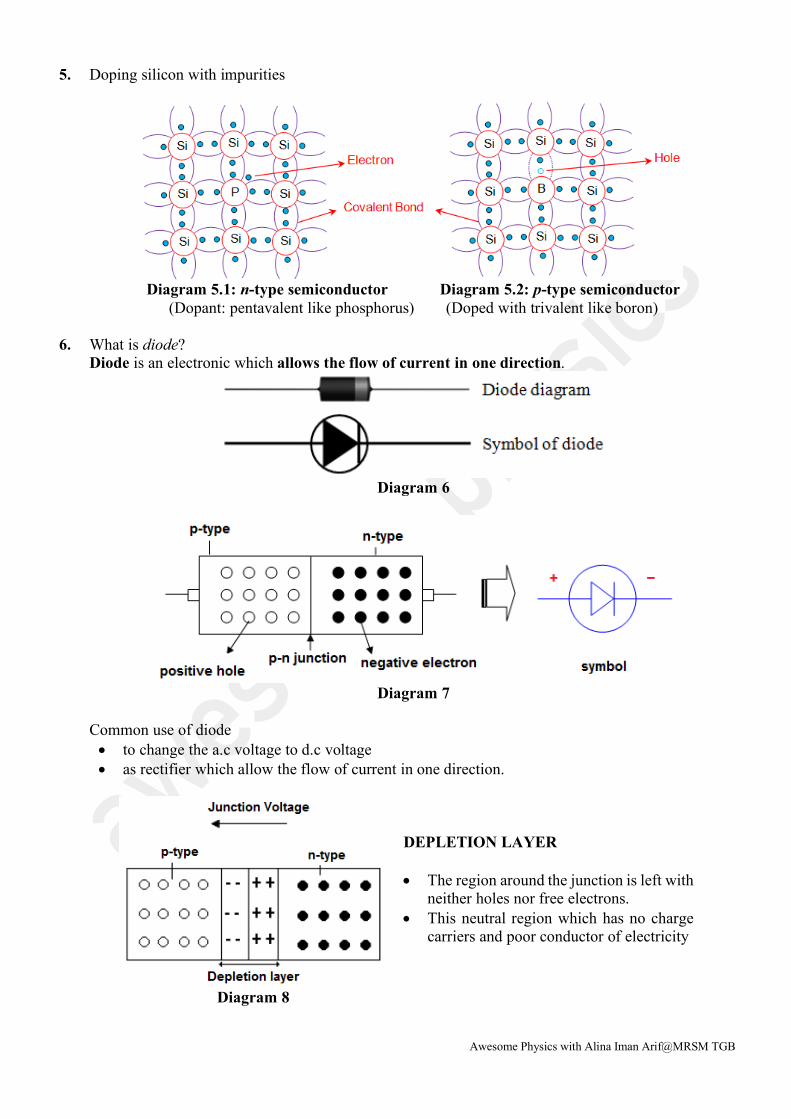
5. Doping silicon with impurities
Diagram 5.1: n-type semiconductor Diagram 5.2: p-type semiconductor
(Dopant: pentavalent like phosphorus) (Doped with trivalent like boron)
6. What is diode? Diode is an electronic which allows the flow of current in one direction.
Diagram 6
Diagram 7
Common use of diode • to change the a.c voltage to d.c voltage • as rectifier which allow the flow of current in one direction.
Diagram 8
DEPLETION LAYER • The region around the junction is left with
neither holes nor free electrons. • This neutral region which has no charge
carriers and poor conductor of electricity
Awesome Physics with Alina Iman Arif@MRSM TGB
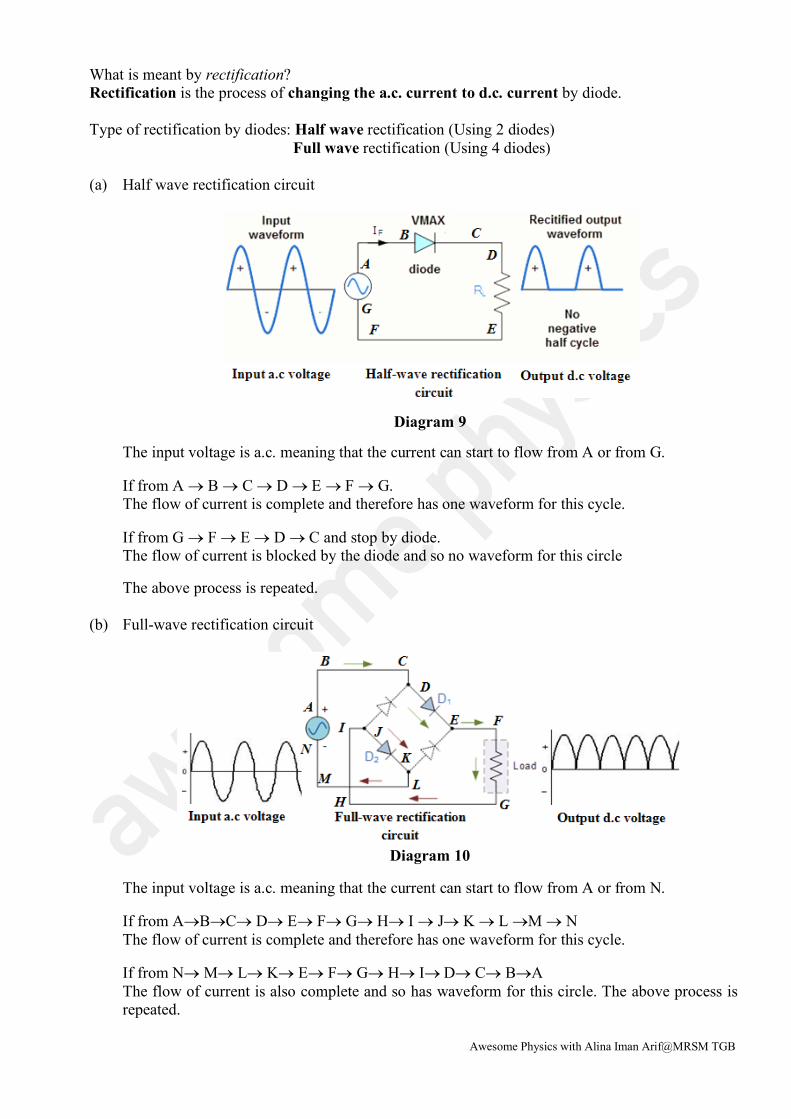
What is meant by rectification? Rectification is the process of changing the a.c. current to d.c. current by diode. Type of rectification by diodes: Half wave rectification (Using 2 diodes) Full wave rectification (Using 4 diodes)
(a) Half wave rectification circuit
Diagram 9
The input voltage is a.c. meaning that the current can start to flow from A or from G. If from A ® B ® C ® D ® E ® F ® G. The flow of current is complete and therefore has one waveform for this cycle. If from G ® F ® E ® D ® C and stop by diode. The flow of current is blocked by the diode and so no waveform for this circle The above process is repeated.
(b) Full-wave rectification circuit
Diagram 10
The input voltage is a.c. meaning that the current can start to flow from A or from N. If from A®B®C® D® E® F® G® H® I ® J® K ® L ®M ® N The flow of current is complete and therefore has one waveform for this cycle. If from N® M® L® K® E® F® G® H® I® D® C® B®A The flow of current is also complete and so has waveform for this circle. The above process is repeated.
Awesome Physics with Alina Iman Arif@MRSM TGB
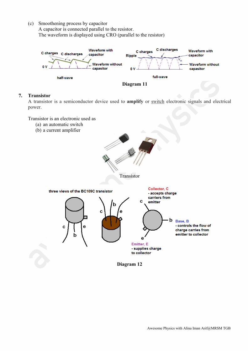
(c) Smoothening process by capacitor A capacitor is connected parallel to the resistor. The waveform is displayed using CRO (parallel to the resistor)
Diagram 11
7. Transistor
A transistor is a semiconductor device used to amplify or switch electronic signals and electrical power. Transistor is an electronic used as
(a) an automatic switch (b) a current amplifier
Transistor
Diagram 12
Awesome Physics with Alina Iman Arif@MRSM TGB
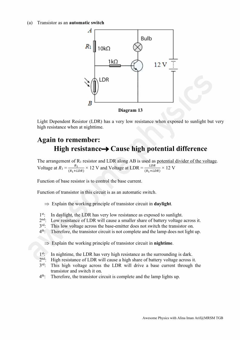
(a)
Transistor as an automatic switch
Diagram 13
Light Dependent Resistor (LDR) has a very low resistance when exposed to sunlight but very high resistance when at nighttime. Again to remember:
High resistance® Cause high potential difference The arrangement of R1 resistor and LDR along AB is used as potential divider of the voltage. Voltage at R1 = 01
(012340) × 12 V and Voltage at LDR = 340
(012340) × 12 V
Function of base resistor is to control the base current. Function of transistor in this circuit is as an automatic switch.
Þ Explain the working principle of transistor circuit in daylight. 1st: In daylight, the LDR has very low resistance as exposed to sunlight. 2nd: Low resistance of LDR will cause a smaller share of battery voltage across it. 3rd: This low voltage across the base-emitter does not switch the transistor on. 4th: Therefore, the transistor circuit is not complete and the lamp does not light up.
Þ Explain the working principle of transistor circuit in nightime.
1st: In nightime, the LDR has very high resistance as the surrounding is dark. 2nd: High resistance of LDR will cause a high share of battery voltage across it. 3rd: This high voltage across the LDR will drive a base current through the
transistor and switch it on. 4th: Therefore, the transistor circuit is complete and the lamp lights up.

Awesome Physics with Alina Iman Arif@MRSM TGB
(b)
Transistor as current amplifier
Diagram 14
1st: The microphone is to convert the sound energy into electrical energy. This
electrical energy will be sent to capacity. 2nd: The capacitor will block the steady current and allow the a.c current to pass
through it. 3rd: The small a.c current will pass to the base of transistor will cause a big
amplification to the output current. Here, the transistor is act as current amplifier.
4th: The loudspeaker now converts the electrical signal back to sound energy again.
Loudspeaker
Capacitor R
S Z
Y Q
P
E
BC
X
6 V dc
Microphone 10 kΩ
40 kΩ

Awesome Physics with Alina Iman Arif@MRSM TGB
8. What are logic gates? Logic gates are the decision makers in electronic systems. They are called gates because they can have many inputs to a device but only give a single output.
GATES SYMBOL BOOLEAN EXPRESSION TRUTH TABLE
AND gate
INPUT OUTPUT A B X 0 0 0 0 1 0 1 0 0 1 1 1
OR gate
INPUT OUTPUT A B X 0 0 0 0 1 1 1 0 1 1 1 1
NOT gate
NOT gate is different from other logic gate as it has only one input with one output.
INPUT OUTPUT A X 0 1 1 0
NAND
gate
INPUT OUTPUT A B X 0 0 1 0 1 1 1 0 1 1 1 0
NOR gate
INPUT OUTPUT A B X 0 0 1 0 1 0 1 0 0 1 1 0
X=A•B
X=A+B
X=A
X=A • B
X=A + B
Awesome Physics with Alina Iman Arif@MRSM TGB
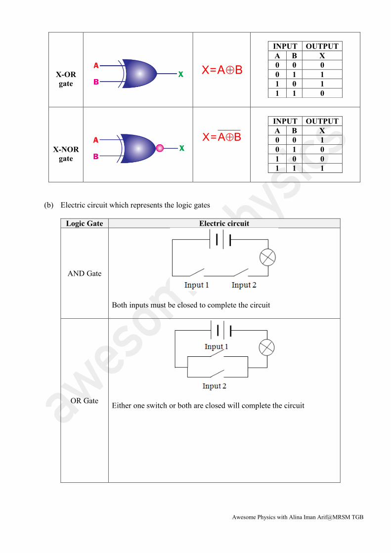
X-OR gate
INPUT OUTPUT A B X 0 0 0 0 1 1 1 0 1 1 1 0
X-NOR gate
INPUT OUTPUT A B X 0 0 1 0 1 0 1 0 0 1 1 1
(b) Electric circuit which represents the logic gates
Logic Gate Electric circuit
AND Gate
Both inputs must be closed to complete the circuit
OR Gate
Either one switch or both are closed will complete the circuit
ÅX=A B
ÅX=A B
Awesome Physics with Alina Iman Arif@MRSM TGB
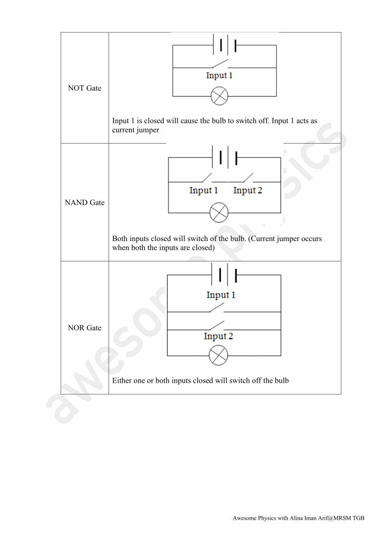
NOT Gate
Input 1 is closed will cause the bulb to switch off. Input 1 acts as current jumper
NAND Gate
Both inputs closed will switch of the bulb. (Current jumper occurs when both the inputs are closed)
NOR Gate
Either one or both inputs closed will switch off the bulb