chapter 3 carrier concentrations in semiconductorsbgonul/dersnotlari/sc/chapter_3.pdf ·...
TRANSCRIPT

CHAPTER 3CHAPTER 3CARRIER CONCENTRATIONS IN CARRIER CONCENTRATIONS IN
CHAPTER 3CHAPTER 3CARRIER CONCENTRATIONS IN CARRIER CONCENTRATIONS IN CARRIER CONCENTRATIONS IN CARRIER CONCENTRATIONS IN
SEMICONDUCTORSSEMICONDUCTORSCARRIER CONCENTRATIONS IN CARRIER CONCENTRATIONS IN
SEMICONDUCTORSSEMICONDUCTORS
Prof. Dr. Beşire GÖNÜL
CARRIER CONCENTRATIONS IN CARRIER CONCENTRATIONS IN SEMICONDUCTORSSEMICONDUCTORS
• Donors and Acceptors
• Fermi level , Ef
• Carrier concentration equations • Carrier concentration equations
• Donors and acceptors both present

Donors and AcceptorsDonors and Acceptors
�� TheThe conductivityconductivity ofof aa purepure(intrinsic)(intrinsic) s/cs/c isis lowlow duedue totothethe lowlow numbernumber ofof freefreecarrierscarriers..
� For an intrinsic semiconductor
� The number of carriers aregenerated by thermally orelectromagnetic radiationfor a pure s/c.
� For an intrinsic semiconductor
n = p = ni
n = concentration of electrons per unit volume
p = concentration of holes per unit volume
ni = the intrinsic carrier concentration of the semiconductor under consideration.

n.p = nn.p = nii22
n = pn = p
number of enumber of e--’s in CB = number of holes in VB’s in CB = number of holes in VB
� This is due to the fact that when an e- makesa transition to the CB, it leaves a hole behindin VB. We have a bipolar (two carrier)in VB. We have a bipolar (two carrier)conduction and the number of holes and e- ‘sare equal.
n.p = ni2
This equation is called as mass-action
law.

TheThe intrinsicintrinsic carriercarrier concentrationconcentration nnii dependsdepends onon;;
�� thethe semiconductorsemiconductor materialmaterial,, andand
�� thethe temperaturetemperature..
n.p = nn.p = nii22
� For silicon at 300 K, ni has a value of 1.4 x 1010 cm-3.
Clearly , equation (n = p = n) can be written as� Clearly , equation (n = p = ni) can be written as
n.p = nn.p = nii22
� This equation is valid for extrinsic as well asintrinsic material.
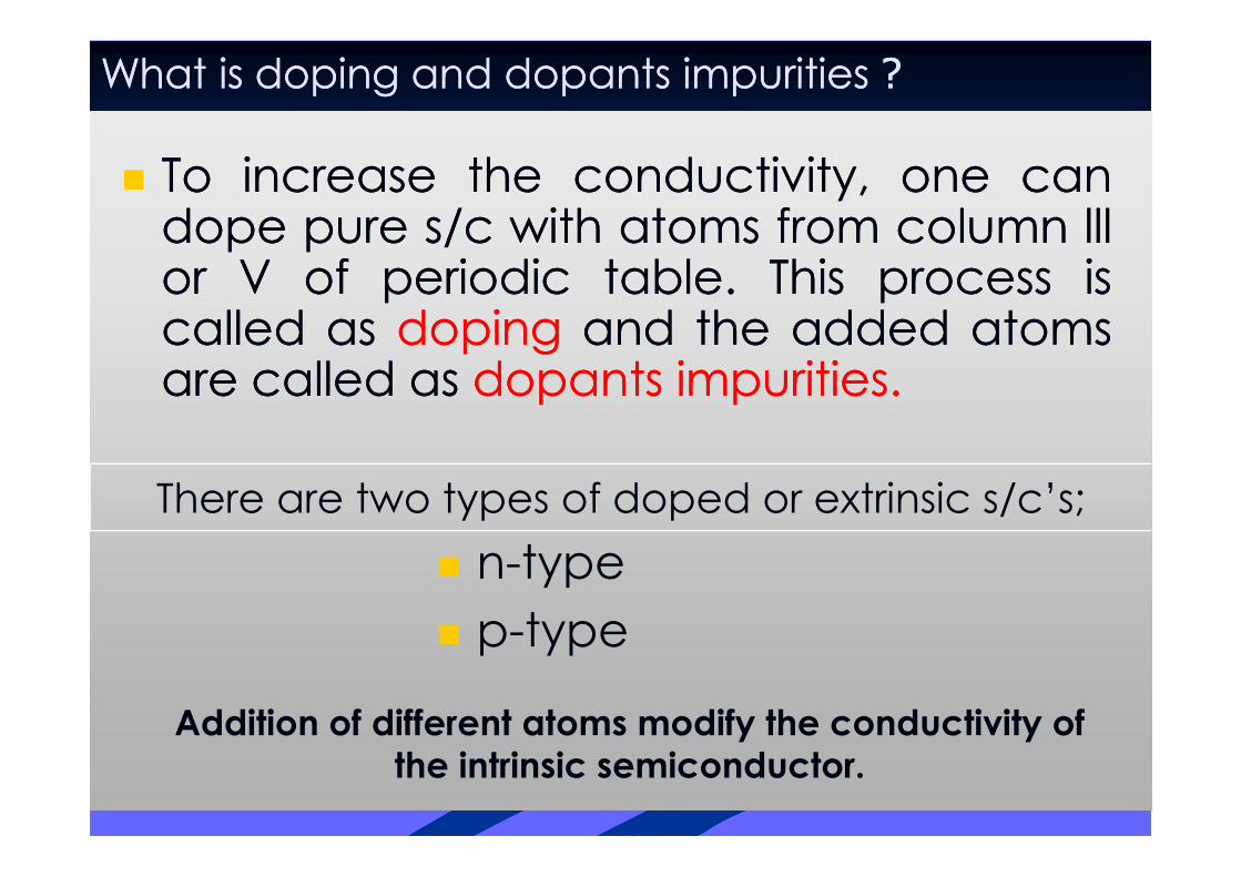
�� ToTo increaseincrease thethe conductivity,conductivity, oneone cancandopedope purepure s/cs/c withwith atomsatoms fromfrom columncolumn lllllloror VV ofof periodicperiodic tabletable.. ThisThis processprocess isiscalledcalled asas dopingdoping andand thethe addedadded atomsatomsareare calledcalled asas dopantsdopants impuritiesimpurities..
What is doping and dopants impurities What is doping and dopants impurities ??
There are two types of doped or extrinsic s/c’s;
� n-type
� p-type
Addition of different atoms modify the conductivity of
the intrinsic semiconductor.

�� pp--type doped semiconductortype doped semiconductor
� Si + Column lll impurity atoms
Boron (B)has three valance
e-’ s
Have four
valance e-’s
Si
Electron
Hole
Bond with missingelectron
Si Si
Si
B
electron
Normal bond with two electrons
� Boron bonding in Silicon
� Boron sits on a lattice side
� p >> n
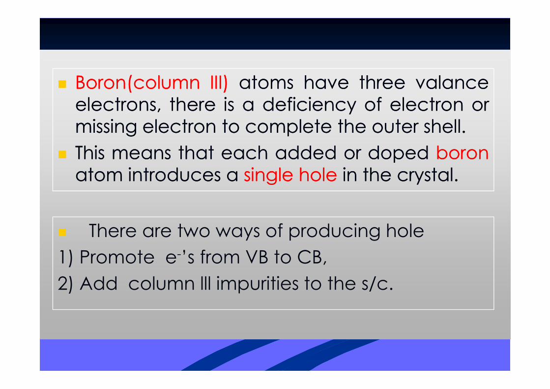
�� Boron(columnBoron(column III)III) atomsatoms havehave threethree valancevalanceelectrons,electrons, therethere isis aa deficiencydeficiency ofof electronelectron orormissingmissing electronelectron toto completecomplete thethe outerouter shellshell..
�� ThisThis meansmeans thatthat eacheach addedadded oror dopeddoped boronboronatomatom introducesintroduces aa singlesingle holehole inin thethe crystalcrystal..
� There are two ways of producing hole
1) Promote e-’s from VB to CB,
2) Add column lll impurities to the s/c.
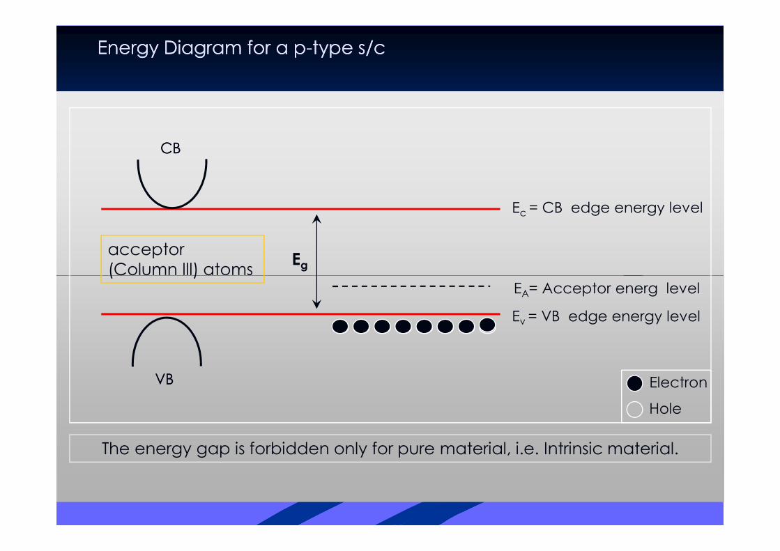
Energy Diagram for a pEnergy Diagram for a p--type s/ctype s/c
Ec = CB edge energy level
Eg
CBCB
acceptor(Column lll) atoms
Ev = VB edge energy level
EA= Acceptor energ level
VBVB
(Column lll) atoms
The energy gap is forbidden only for pure material, i.e. Intrinsic material.
Electron
Hole

�� TheThe impurityimpurity atomsatoms fromfrom columncolumn llllll occupyoccupy atat anan energyenergy levellevel
withinwithin EEgg .. TheseThese levelslevels cancan bebe
1.1. ShallowShallow levelslevels whichwhich isis closeclose toto thethe bandband edge,edge,
2.2. DeepDeep levelslevels whichwhich lieslies almostalmost atat thethe midmid ofof thethe bandband gapgap..
� If the EA level is shallow i.e. close to the VB edge, each addedboron atom accepts an e- from VB and have a full
p-type semiconductor
boron atom accepts an e from VB and have a fullconfiguration of e-’s at the outer shell.
� These atoms are called as acceptor atoms since they acceptan e- from VB to complete its bonding. So each acceptoratom gives rise a hole in VB.
� The current is mostly due to holes since the number of holes aremade greater than e-’s.

Holes Holes = = pp = majority carriers= majority carriers
Electrons Electrons = = nn = minority carriers= minority carriers
Majority and minority carriers in a pMajority and minority carriers in a p--type semiconductortype semiconductor
t2
t1
Electric field direction
Holes movement as a t2
t3
Holes movement as a function of applied electric field
Hole movement direction
Electron movement direction
Ec
Ev
Ea
Eg
Si
Electron
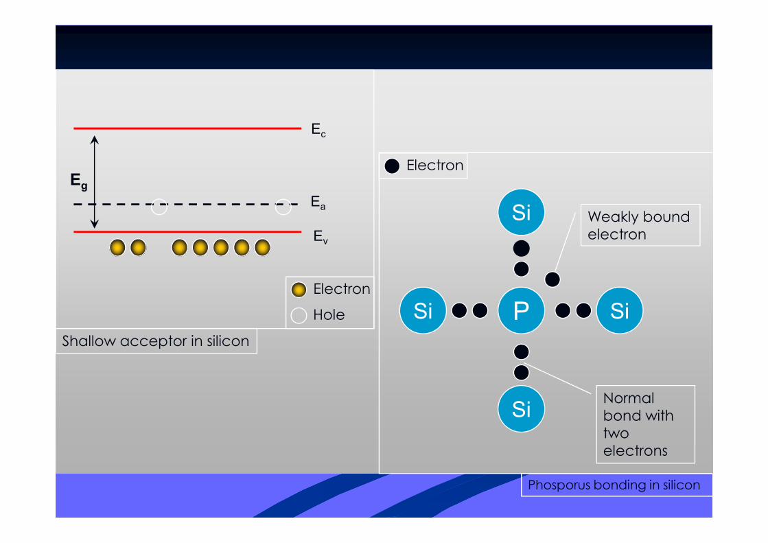
Weakly bound electron
Electron
Hole
Shallow acceptor in silicon
Si Si
Si
P
Normal bond with two electrons
Phosporus bonding in silicon
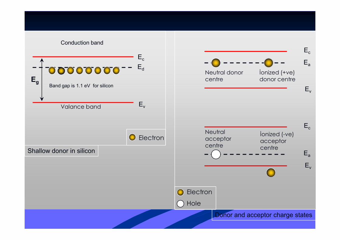
Ec
Ev
Ed
Eg
Valance band
Conduction band
Band gap is 1.1 eV for silicon
Neutral donor centre
Đonized (+ve)donor centre
Ec
Ev
Ea
Electron
Shallow donor in silicon
Donor and acceptor charge states
Electron
Hole
Neutral acceptor centre
Đonized (-ve)acceptor centre
Ec
Ev
Ea
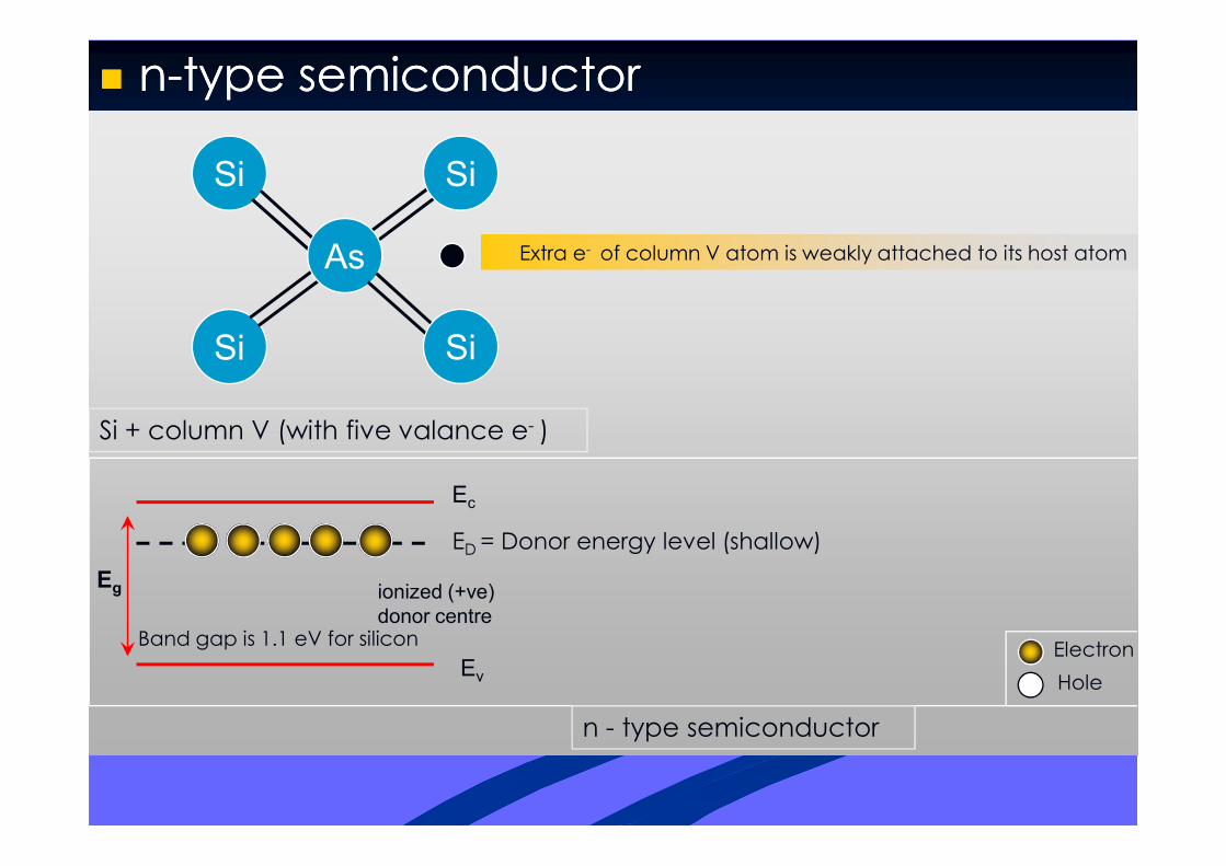
Extra e- of column V atom is weakly attached to its host atom
�� nn--type semiconductortype semiconductor
Si
Si
Si
As
Si
Si + column V (with five valance e- )Si + column V (with five valance e- )
ionized (+ve)
donor centre
Ec
Ev
ED = Donor energy level (shallow)
Band gap is 1.1 eV for silicon
Hole
Electron
Eg
n - type semiconductor
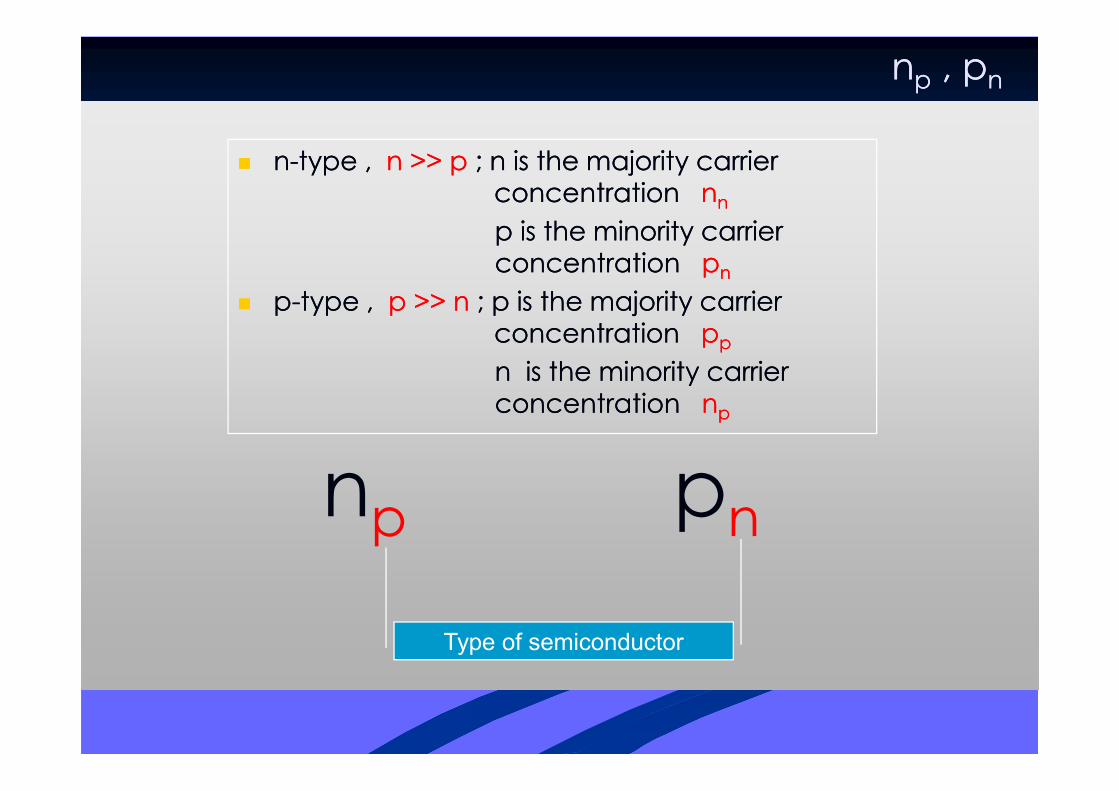
nnpp , p, pnn
�� nn--type , type , n >> pn >> p ; n is the majority carrier ; n is the majority carrier concentration concentration nnnn
p is the minority carrier p is the minority carrier concentration concentration ppnn
�� pp--type , type , p >> np >> n ; p is the majority carrier ; p is the majority carrier concentration concentration pppp
n is the minority carrier n is the minority carrier concentration concentration nnconcentration concentration nnpp
np pn
Type of semiconductor
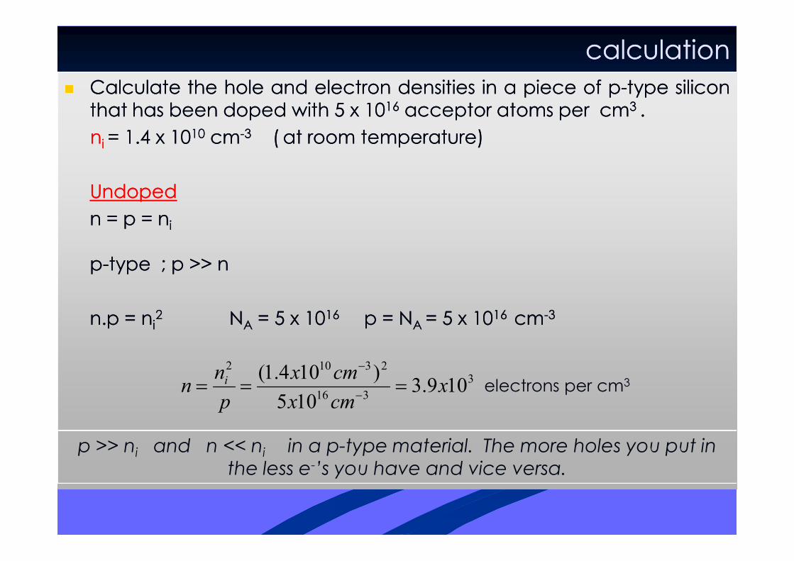
calculationcalculation�� CalculateCalculate thethe holehole andand electronelectron densitiesdensities inin aa piecepiece ofof pp--typetype siliconsilicon
thatthat hashas beenbeen dopeddoped withwith 55 xx 10101616 acceptoracceptor atomsatoms perper cmcm33 ..
nnii == 11..44 xx 10101010 cmcm--33 (( atat roomroom temperature)temperature)
UndopedUndoped
nn == pp == nnii
pp--typetype ;; pp >>>> nn
nn..pp == nnii22 NNAA == 55 xx 10101616 pp == NNAA == 55 xx 10101616 cmcm--33
3
316
23102
109.3105
)104.1(x
cmx
cmx
p
nn i === −
−
electrons per cm3
p >> ni and n << ni in a p-type material. The more holes you put in
the less e-’s you have and vice versa.

Fermi level , EFermi level , EFF
�� ThisThis isis aa referencereference energyenergy levellevel atat whichwhich thethe probabilityprobability ofof occupationoccupationbyby anan electronelectron isis ½½..
�� SinceSince EEff isis aa referencereference levellevel thereforetherefore itit cancan appearappear anywhereanywhere inin thetheenergyenergy levellevel diagramdiagram ofof aa S/CS/C ..
�� FermiFermi energyenergy levellevel isis notnot fixedfixed..�� OccupationOccupation probabilityprobability ofof anan electronelectron andand holehole cancan bebe determineddetermined
byby FermiFermi--DiracDirac distributiondistribution function,function, FFFDFD ;;
EEFF == FermiFermi energyenergy levellevelkkBB == BoltzmanBoltzman constantconstantTT == TemperatureTemperature
)exp(1
1
Tk
EEF
B
FFD −
+=

�� EE isis thethe energyenergy levellevel underunder investigationinvestigation..
�� FFFDFD determinesdetermines thethe probabilityprobability ofof thethe energyenergy levellevel EE beingbeingoccupiedoccupied byby electronelectron..
)exp(1
1
Tk
EEF
B
FFD −
+=
11
Fermi level , EFermi level , EFF
�� determinesdetermines thethe probabilityprobability ofof notnot findingfinding ananelectronelectron atat anan energyenergy levellevel EE;; thethe probabilityprobability ofof findingfinding aaholehole ..
FD
FDF
f
fEEif
−
=+
=→=
1
2
1
0exp1
1

Carrier concentration equationsCarrier concentration equations
TheThe numbernumber density,density, ii..ee..,, thethe numbernumber ofof electronselectronsavailableavailable forfor conductionconduction inin CBCB isis
3 / 2*
2
22 exp ( )
exp ( ) exp( )
n C F
C F F iC i
m kT E En
h kT
E E E En N n n
kT kT
π −= −
− −
= − =
3 / 2*
2
22 exp ( )
exp ( ) exp( )
p F V
F V i FV i
m kT E Ep
h kT
E E E Ep N p n
kT kT
π −= −
− −
= − =
exp ( ) exp( )C in N n nkT kT
= − =
TheThe numbernumber density,density, ii..ee..,, thethe numbernumber ofof holesholes availableavailableforfor conductionconduction inin VBVB isis

Donors and acceptors both presentDonors and acceptors both present
�� BothBoth donorsdonors andand acceptorsacceptors presentpresent inin aa s/cs/c iningeneralgeneral.. HoweverHowever oneone willwill outnumberoutnumber thethe otherotheroneone..
�� InIn anan nn--typetype materialmaterial thethe numbernumber ofof donordonorconcentrationconcentration isis significantlysignificantly greatergreater thanthan thatthatofof thethe acceptoracceptor concentrationconcentration..Similarly,Similarly, inin aa pp--typetype materialmaterial thethe numbernumber ofof�� Similarly,Similarly, inin aa pp--typetype materialmaterial thethe numbernumber ofofacceptoracceptor concentrationconcentration isis significantlysignificantly greatergreaterthanthan thatthat ofof thethe donordonor concentrationconcentration..
�� AA pp--typetype materialmaterial cancan bebe convertedconverted toto anan nn--typetype materialmaterial oror vicevice versaversa byby meansmeans ofof addingaddingproperproper typetype ofof dopantdopant atomsatoms.. ThisThis isis inin factfact howhowpp--nn junctionjunction diodesdiodes areare actuallyactually fabricatedfabricated..

�� How does the position of the Fermi Level change withHow does the position of the Fermi Level change with
(a)(a) increasing increasing donor concentrationdonor concentration, and, and
(b)(b) increasing increasing acceptor concentrationacceptor concentration ??
Worked exampleWorked example
(a) We shall use equation
E E−
Đf n is increasing then the quantity EC-EF must be decreasingi.e. as the donor concentration goes up the Fermi level movestowards the conduction band edge Ec.
exp ( )C FC
E En N
kT
−= −
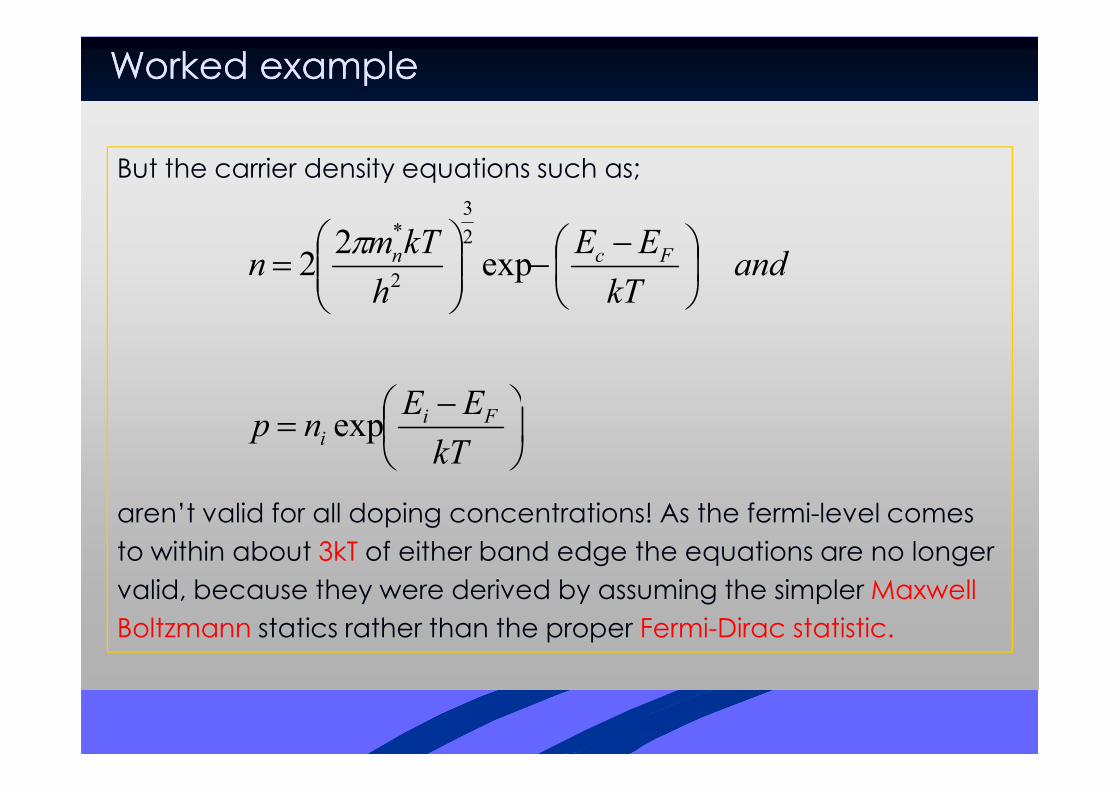
Worked exampleWorked example
But the carrier density equations such as;
−
−−
=
EE
andkT
EE
h
kTmn Fcn exp
22
2
3
2
*π
aren’t valid for all doping concentrations! As the fermi-level comes
to within about 3kT of either band edge the equations are no longer
valid, because they were derived by assuming the simpler Maxwell
Boltzmann statics rather than the proper Fermi-Dirac statistic.
−=
kT
EEnp Fii exp

Worked example Worked example
EEgg/2/2 EEgg/2/2EEgg/2/2
EECC
EEVV
EEF1F1
EEF2F2 EEF3F3
n3n1 n2
n3 > n2 > n1
EEgg/2/2 EEgg/2/2 EEgg/2/2
EECC
EEVV
EEF1F1
EEF2F2EEF3F3
p1 p3p2
p3 > p2 > p1

Worked exampleWorked example
(b) Considering the density of holes in valence band;
It is seen that as the acceptor concentration increases, Fermi-level
moves towards the valance band edge. These results will be used in
−−=
kT
EENp VFv exp
moves towards the valance band edge. These results will be used in
the construction of device (energy) band diagrams.
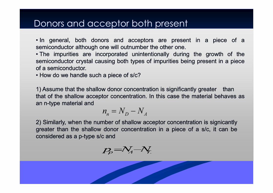
Donors and acceptor both presentDonors and acceptor both present
•• InIn general,general, bothboth donorsdonors andand acceptorsacceptors areare presentpresent inin aa piecepiece ofof aa
semiconductorsemiconductor althoughalthough oneone willwill outnumberoutnumber thethe otherother oneone..
•• TheThe impuritiesimpurities areare incorporatedincorporated unintentionallyunintentionally duringduring thethe growthgrowth ofof thethe
semiconductorsemiconductor crystalcrystal causingcausing bothboth typestypes ofof impuritiesimpurities beingbeing presentpresent inin aa piecepiece
ofof aa semiconductorsemiconductor..
•• How do we handle such a piece of s/c?How do we handle such a piece of s/c?
11)) AssumeAssume thatthat thethe shallowshallow donordonor concentrationconcentration isis significantlysignificantly greatergreater thanthan
thatthat ofof thethe shallowshallow acceptoracceptor concentrationconcentration.. InIn thisthis casecase thethe materialmaterial behavesbehaves asas
n D An N N= −22)) Similarly,Similarly, whenwhen thethe numbernumber ofof shallowshallow acceptoracceptor concentrationconcentration isis signicantlysignicantly
greatergreater thanthan thethe shallowshallow donordonor concentrationconcentration inin aa piecepiece ofof aa s/c,s/c, itit cancan bebe
consideredconsidered asas aa pp--typetype s/cs/c andand
thatthat ofof thethe shallowshallow acceptoracceptor concentrationconcentration.. InIn thisthis casecase thethe materialmaterial behavesbehaves asas
anan nn--typetype materialmaterial andand

�� For the case For the case NNAA>N>ND D , i.e. , i.e. for pfor p--type materialtype material
Donors and acceptor both present Donors and acceptor both present
2.
0
p p i
p A D P p D p A
n p n
n N N p p N n N− +
=
+ = + ⇒ + − − =
22 20 ( ) 0i
p p D A p D A p i
p
np p N N p N N p n
p
⋅ + − − = ⇒ + − − =

Donors and acceptor both presentDonors and acceptor both present
( )
22 2
1,2
12 22
4( ) 0 , solving for ;
2
14
2
p D A p i p
p A D A D i
b b acp N N p n p x
a
p N N N N n
− −+ − − = =
= − + − +
m
majority( )
2
2p A D A D i
ip
p
nn
p
= minority

Donors and acceptor both presentDonors and acceptor both present�� For the case For the case NNDD>N>NAA , , i.e. ni.e. n--type materialtype material
22
22 2
.
0
0 ( ) 0
in n i n
n
n A D n n A n D
in n A D n A D n i
n
nn p n p
n
n N N P n N p N
nn n N N n N N n n
n
= ⇒ =
+ = + ⇒ + − − =
⋅ + − − = ⇒ + − − =
( )
2
1 , 2
12 22
2
4so lv in g fo r n ;
2
14
2
n
n
n D A D A i
in
n
n
b b a cx
a
n N N N N n
np
n
− −=
= − + − +
=
m