chapter 29 transistor amplifiers. 2 use of capacitors in amplifier circuits capacitor review...
TRANSCRIPT

Chapter 29
Transistor Amplifiers

2
Use of Capacitors in Amplifier Circuits
• Capacitor review– Store electrical charge– Impedance:
– ∞ impedance at dc– Impedance decreases at higher frequencies
1[ ]
2CXfCπ
= Ω

3
Use of Capacitors in Amplifier Circuits
• Capacitors– Block dc between stages– Can be designed to readily pass ac

4
Use of Capacitors in Amplifier Circuits
• Coupling capacitors– At “high” frequencies
– For R = Rin + RS, select capacitor so XC ≤ 0.1 R– Referred to as “stiff coupling”
inin S
in S
RV V
R R
⎛ ⎞=⎜ ⎟+⎝ ⎠

5
Use of Capacitors in Amplifier Circuits
• Bypass capacitors– Emitter resistor, Re used for biasing
– Ce is a short circuit at high frequencies
– Re has no effect on amplification when Ce is present
– Select XC ≤ 0.1R

6
Use of Capacitors in Amplifier Circuits

7
Use of Capacitors in Amplifier Circuits
• Capacitors– Couple desired ac signals between stages– Bypass unwanted ac signals to ground

8
Use of Capacitors in Amplifier Circuits
• Circuit analysis– If XC ≤ 0.1R
– Replace C with O.C. to determine dc I and V– Replace C with S.C. to determine ac i and v

9
BJT Small-Signal Models
• T-Equivalent Model– ie = ib + ic
– ie = (β + 1)ib –
– Simple– Good enough for most applications
2625oe
EQ
mvr at C
I=

10
BJT Small-Signal Models
B
E
rc
iCie
ib βacib

11
BJT Small-Signal Models• Models
– T-equivalent model simpler– h-parameter model more accurate
– hfe (h-model) = βac (T-model) [βac ≈ βdc]
– h-parameters dependent on Q-point– BJT is a current amplifier (current source in
both models)

12
BJT Small-Signal Models• h-parameter model
– More complex– Better for ac operation– Common Emitter model
• hie = input impedance (Ω)
• hre = reverse voltage transfer ratio (unitless)
• hfe = forward current transfer ratio (unitless)
• hoe = output admittance (S)
hfeib
B
E
hie
iC
ie
ib
hreVce
1/hoe

13
Calculating Av, zin, zout, and Ai of a Transistor Amplifier
• Voltage Gain, Av
– Output voltage divided by input voltage
• Input Impedance, zin
– Input voltage divided by input current in
inin
in
outv
i
vz
v
vA
=
=

14
Calculating Av, zin, zout, and Ai of a Transistor Amplifier
• Output Impedance, zout
• Current Gain, Ai
• Power Gain, Ap
out(SC)
out(OC)out i
vz =
in
outi i
iA =
in
outp P
PA =

15
Common-Emitter Amplifier
• General BJT circuit analysis– Find operating point– Determine ac parameters (T- or h- models)– Remove dc V sources & replace with S.C.’s– Replace coupling & bypass C’s with S.C.’s– Replace BJT with circuit model– Solve resulting circuit

16
Common-Emitter Amplifier• ac equivalent of fixed-bias CE amplifier
using h-parameter model

17
Common-Emitter Amplifier• Equations for h-parameter model for
fixed-bias CE amplifier– Circuit voltage gain a function of
• Model forward current transfer ratio, hfe • Model input impedance, hie • Circuit collector resistance, RC • Circuit load resistance, RL
( )ie
LCfev h
RRhA −=

18
Common-Emitter Amplifier
• Circuit current gain a function of– Same parameters, plus– Fixed bias resistance, RB
( )( )ieBLC
CBfei hRRR
RRhA
++=

19
Common-Emitter Amplifier
• Equations for h-parameter model for fixed-bias CE amplifier– Circuit input impedance a function of
• Model forward current transfer ratio, hfe
• Model input impedance, hie
ieBin hRz =

20
Common-Emitter Amplifier
• Circuit output impedance a function of
– Collector resistance (model output admittance), hoe very low Cout Rz =

21
ac Load Line• Q-point is on dc load line
• ac load line determines maximum undistorted output
• Can calculate maximum power
• Q-point also on ac load line
• ac load line has different slope

22
ac Load Line
• CE amplifier circuit
23
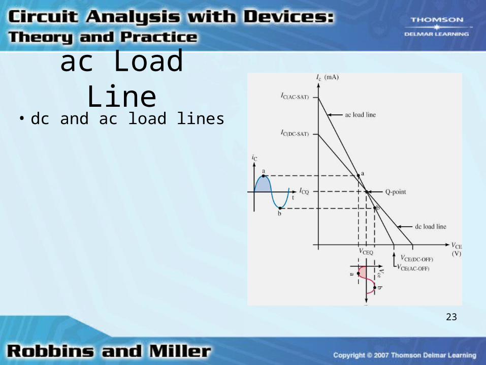
ac Load Line• dc and ac load lines

24
ac Load Line
• Equations of ac load line
• Consider– CE amplifier circuit– dc load line
( )CE C C E
CEC
C E
C CQ c
CE CEQ ce
v i r r
VI
r r
i O i
v V v
=− +
=+
= +
= +

25
Common-Collector Amplifier• Important characteristics
– High input impedance– Low output impedance
– vout in-phase with vin
– vout ≈ vin

26
Common-Collector Amplifier• Important characteristics
– Large current gain – Input voltage measured at base– Output voltage measured at emitter

27
Common-Collector Amplifier
• Common-Collector circuit

28
Common-Collector Amplifier
• Circuit gains and impedances– Av ≈ 1
– zin = RB||zin(Q)
– close to hfe
– very small( )
||
1
V ini
L
S Bout Q e
fe
A zA
R
R Rz r
h
=−
= =+

29
FET Small-Signal Model
• Voltage controlled amplifier
• Small-signal model same for JFETs & MOSFETs
• High input impedance
• is = id
gmvgs
G
S
∞
id
is
ig=0
Vgs rd
D
+-

30
FET Small-Signal Model
• gm is transconductance
• gm is slope of transfer curve

31
FET Small-Signal Model• Equations
– Definition
– Maximum
– Measured
( )
( )
2
1
Dm
GS
DSSmo
Gs OFF
GSQm mo
GS OFF
Ig
V
Ig
V
Vg g
V
Δ=
Δ
=
⎛ ⎞= −⎜ ⎟⎜ ⎟
⎝ ⎠

32
Common-Source Amplifier• Analysis
– Similar to BJT using h-parameter model– First determine bias– Find dc operating point (Q-point)
– Determine gm

33
Common-Source Amplifier
• A common-source circuit

34
Common-Source Amplifier• Equations
– No current input– Voltage gain dependent on
gm and RD
– Input impedance is RG || ∞
– Output impedance approximately drain resistance
V m D
in G
out D
A g R
z R
z R
≈−=≈

35
Common-Source Amplifier
• D-MOSFETs– Analysis same as JFETs – Except operation in enhancement region

36
Common-Source Amplifier
• E-MOSFETs– Find IDSQ, VGSQ, and VDSQ at Q-point
– Solve for gm of amplifier
– Sketch ac equivalent circuit
– Determine Av, zin, and zout of amplifier

37
Common-Drain (Source Follower) Amplifier
• Av < 1
• vout in phase with vin
• Input impedance very high
• Output impedance low
• Main application: Buffer

38
Troubleshooting a Transistor Amplifier Circuit
• Incorrect placement of electrolytic capacitors– Noisy output signal– Capacitor as an antenna– Generally 60 Hz added

39
Troubleshooting a Transistor Amplifier Circuit
• Correct placement– Check proper polarity– Replace faulty capacitors

40
Troubleshooting a Transistor Amplifier Circuit
• Faulty or incorrectly placed capacitor– Measured Av different from theoretical Av
– Faulty capacitor behaves like an open circuit– Faulty capacitor can develop internal short

41
Troubleshooting a Transistor Amplifier Circuit
• Troubleshooting steps– Remove ac signal sources from circuit– Calculate theoretical Q-point– Measure to determine actual Q-point– Verify capacitors are correctly placed– Ensure connections, especially ground wires,
as short as possible

42
Troubleshooting a Transistor Amplifier Circuit
• Distorted output signal usually the result of too large an input signal