chapter 11: system design methodology digital system designs and practices using verilog hdl and...
TRANSCRIPT

Chapter 11: System Design Methodology
11-1Digital System Designs and Practices Using Verilog HDL and FPGAs @ 2008, John Wiley
Ders 9: RTL Design
Chapter 11: System Design Methodology
11-2Digital System Designs and Practices Using Verilog HDL and FPGAs @ 2008, John Wiley2
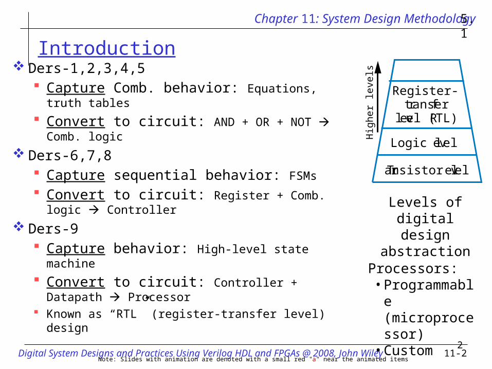
Introduction Ders-1,2,3,4,5
Capture Comb. behavior: Equations, truth tables
Convert to circuit: AND + OR + NOT Comb. logic
Ders-6,7,8 Capture sequential behavior: FSMs
Convert to circuit: Register + Comb. logic Controller
Ders-9 Capture behavior: High-level state machine
Convert to circuit: Controller + Datapath Processor
Known as “RTL” (register-transfer level) design
Note: Slides with animation are denoted with a small red "a" near the animated items
Transistor level
Logic level
Register-transfer
level (RTL)
Levels of digital design abstraction
Hig
her
leve
ls
Processors:• Programmable
(microprocessor)• Custom
5.1
Chapter 11: System Design Methodology
11-3Digital System Designs and Practices Using Verilog HDL and FPGAs @ 2008, John Wiley
Register-Transfer-Level Design
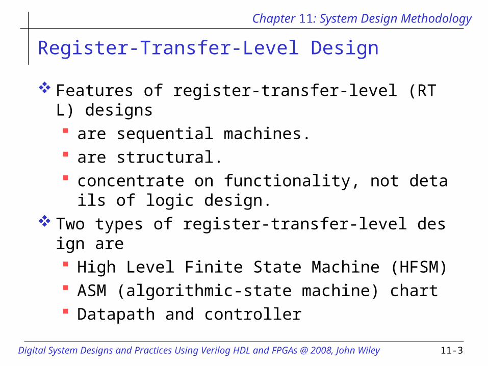
Features of register-transfer-level (RTL) designs are sequential machines. are structural. concentrate on functionality, not details of logic design.
Two types of register-transfer-level design are High Level Finite State Machine (HFSM) ASM (algorithmic-state machine) chart Datapath and controller

Chapter 11: System Design Methodology
11-4Digital System Designs and Practices Using Verilog HDL and FPGAs @ 2008, John Wiley
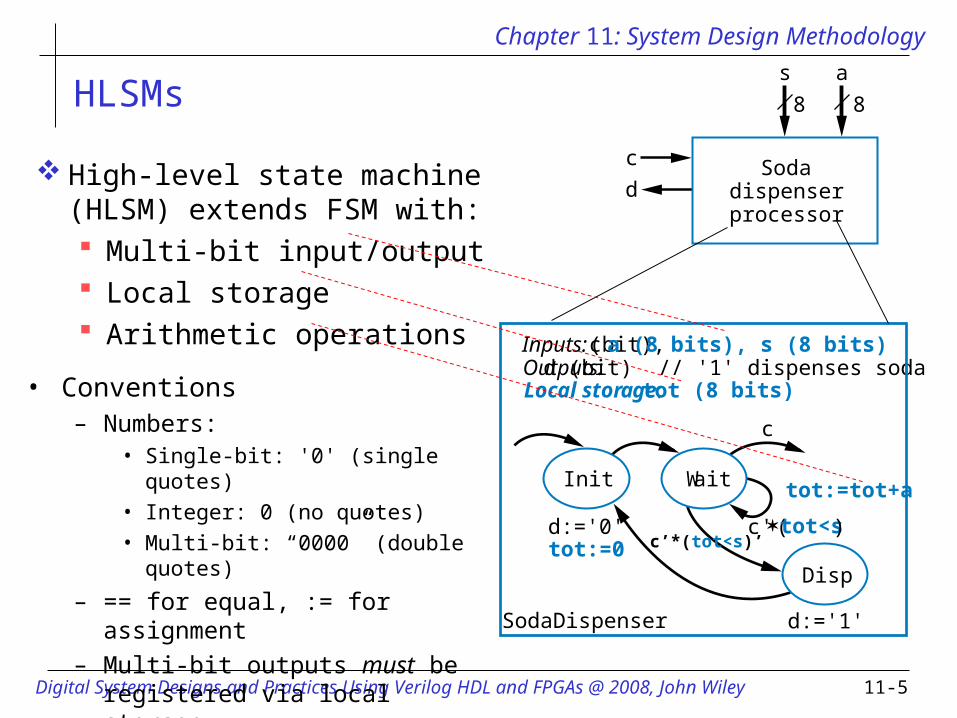
High-Level State Machines (HLSMs) Some behaviors too complex for
equations, truth tables, or FSMs Ex: Soda dispenser
c: bit input, 1 when coin deposited a: 8-bit input having value of
deposited coin s: 8-bit input having cost of a soda d: bit output, processor sets to 1
when total value of deposited coins equals or exceeds cost of a soda
FSM can’t represent… 8-bit input/output Storage of current total Addition (e.g., 25 + 10)
as
cd
Sodadispenserprocessor
25
1 025
1
1
500
0
0
0
tot: 25tot: 50
a
as
cd
Sodadispenserprocessor
Chapter 11: System Design Methodology
11-5Digital System Designs and Practices Using Verilog HDL and FPGAs @ 2008, John Wiley
HLSMs
High-level state machine (HLSM) extends FSM with: Multi-bit input/output Local storage Arithmetic operations Inputs: c (bit),a (8 bits), s (8 bits)
Outputs: d (bit) // '1' dispenses sodaLocal storage: tot (8 bits)
Wait
Disp
Init
d:='0'tot:=0 c’*(tot<s)’
c'(tot<s)
d:='1'
c
tot:=tot+a
SodaDispenser
8 8
as
c
dSoda
dispenserprocessor
• Conventions– Numbers:
• Single-bit: '0' (single quotes)• Integer: 0 (no quotes)• Multi-bit: “0000” (double quotes)
– == for equal, := for assignment
– Multi-bit outputs must be registered via local storage
– // precedes a comment
Chapter 11: System Design Methodology
11-6Digital System Designs and Practices Using Verilog HDL and FPGAs @ 2008, John Wiley
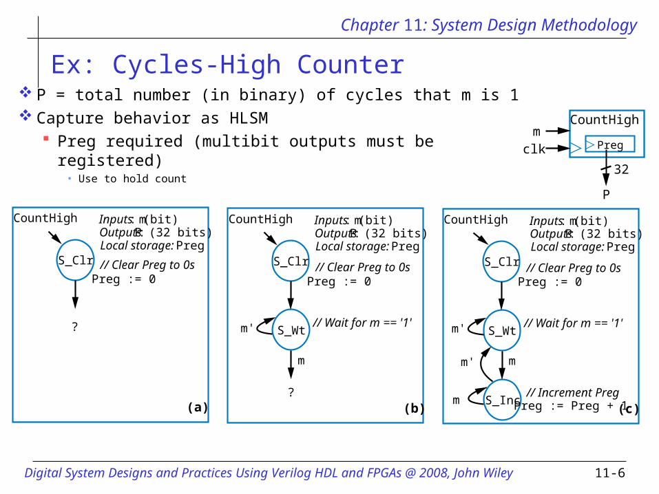
Ex: Cycles-High Counter P = total number (in binary) of cycles that m is 1 Capture behavior as HLSM
Preg required (multibit outputs must be registered)• Use to hold count P
mCountHigh
clk
32
S_Clr
S_Wtm'
S_Incm
mm'
Preg := 0
Preg := Preg + 1
// Clear Preg to 0s
// Wait for m == '1'
// Increment Preg
CountHigh Inputs: m (bit)Outputs: P (32 bits)Local storage: Preg
(c)
S_Clr
Preg := 0// Clear Preg to 0s
CountHigh Inputs: m (bit)Outputs: P (32 bits)Local storage: Preg
(a)
?
S_Clr
S_Wtm'
m
Preg := 0// Clear Preg to 0s
// Wait for m == '1'
CountHigh Inputs: m (bit)Outputs: P (32 bits)Local storage: Preg
(b)?
Preg

Chapter 11: System Design Methodology
11-7Digital System Designs and Practices Using Verilog HDL and FPGAs @ 2008, John Wiley
Example: Laser-Based Distance Measurer
Laser-based distance measurement – pulse laser, measure time T to sense reflection Laser light travels at speed of light, 3*108 m/sec Distance is thus D = (T sec * 3*108 m/sec) / 2
Object ofinterest
D
2D = T sec * 3*108 m/sec
sensor
laser
T (in seconds)
Chapter 11: System Design Methodology
11-8Digital System Designs and Practices Using Verilog HDL and FPGAs @ 2008, John Wiley
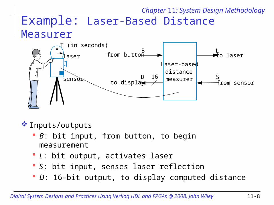
Example: Laser-Based Distance Measurer
Inputs/outputs B: bit input, from button, to begin measurement L: bit output, activates laser S: bit input, senses laser reflection D: 16-bit output, to display computed distance
sensor
laser
T (in seconds)
Laser-baseddistancemeasurer16
from button
to displayS
L
D
Bto laser
from sensor
Chapter 11: System Design Methodology
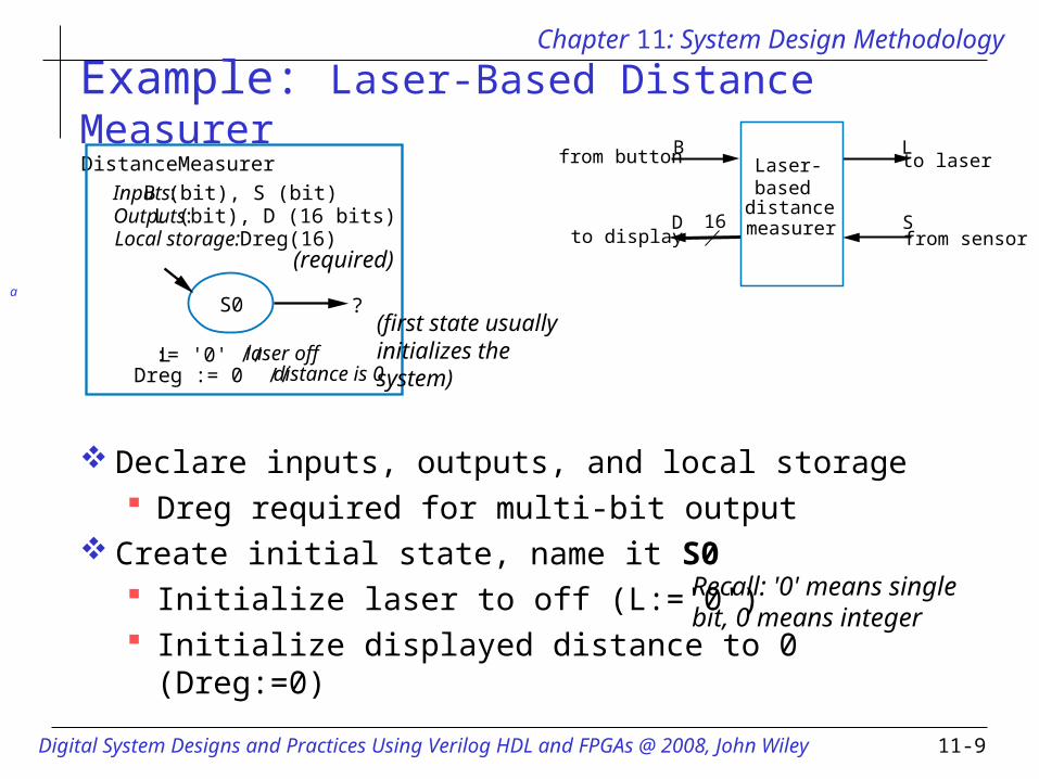
11-9Digital System Designs and Practices Using Verilog HDL and FPGAs @ 2008, John Wiley
Example: Laser-Based Distance Measurer
Declare inputs, outputs, and local storage Dreg required for multi-bit output
Create initial state, name it S0 Initialize laser to off (L:='0') Initialize displayed distance to 0 (Dreg:=0)
Laser-based
distancemeasurer16
from button
to displayS
L
D
Bto laser
from sensor
a
Inputs: B (bit), S (bit)Outputs: L (bit), D (16 bits)Local storage: Dreg(16)
S0 ?
L := '0' // laser offDreg := 0 // distance is 0
DistanceMeasurer
(required)
(first state usually initializes the system)
Recall: '0' means single bit, 0 means integer

Chapter 11: System Design Methodology
11-10Digital System Designs and Practices Using Verilog HDL and FPGAs @ 2008, John Wiley
Example: Laser-Based Distance Measurer
Add another state, S1, that waits for a button press B' – stay in S1, keep waiting B – go to a new state S2
Q: What should S2 do? A: Turn on the lasera
Laser-based
distancemeasurer16
from button
to displayS
L
D
Bto laser
from sensor
S0
L := '0'Dreg := 0
S1 ?
B' // button not pressed
B// buttonpressed
S0
DistanceMeasurer ...
Chapter 11: System Design Methodology
11-11Digital System Designs and Practices Using Verilog HDL and FPGAs @ 2008, John Wiley
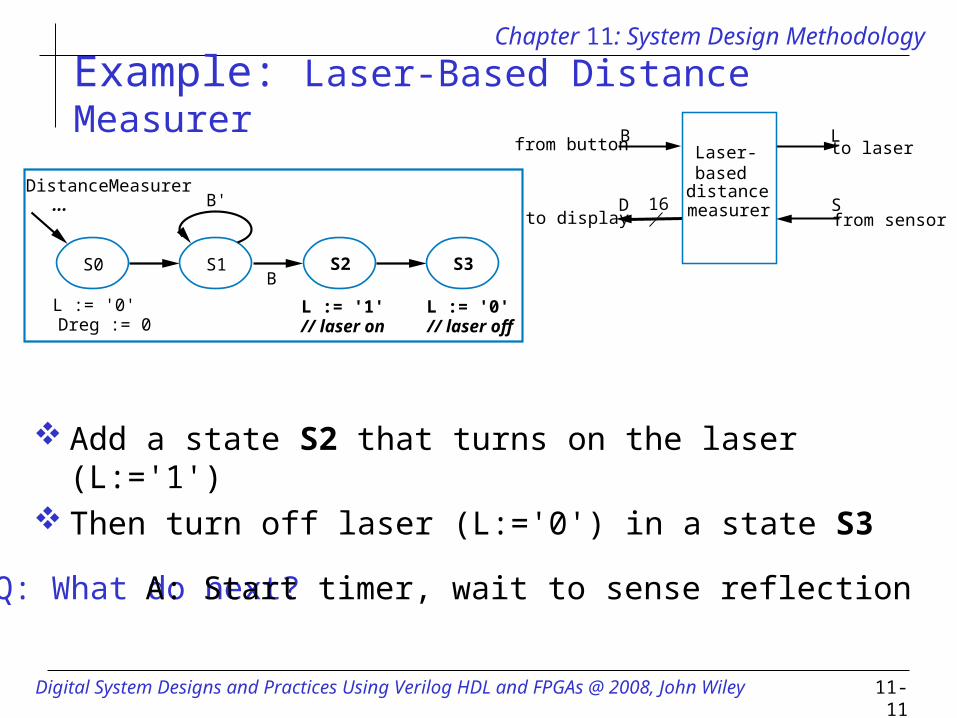
Example: Laser-Based Distance Measurer
Add a state S2 that turns on the laser (L:='1') Then turn off laser (L:='0') in a state S3
Q: What do next? A: Start timer, wait to sense reflection
Laser-based
distancemeasurer16
from button
to displayS
L
D
Bto laser
from sensor
DistanceMeasurer ...
S0 S1
L := '0'Dreg := 0
S2
L := '1'// laser on
S3
L := '0'// laser off
B'
B
Chapter 11: System Design Methodology
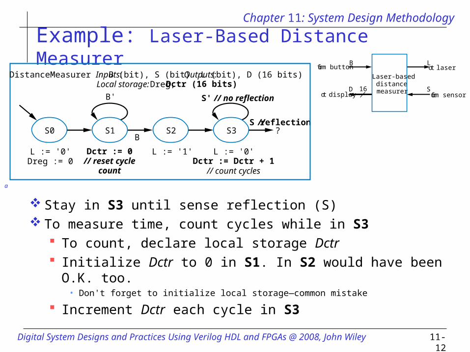
11-12Digital System Designs and Practices Using Verilog HDL and FPGAs @ 2008, John Wiley
Example: Laser-Based Distance Measurer
Stay in S3 until sense reflection (S) To measure time, count cycles while in S3
To count, declare local storage Dctr Initialize Dctr to 0 in S1. In S2 would have been O.K. too.
• Don't forget to initialize local storage—common mistake
Increment Dctr each cycle in S3
Laser-baseddistancemeasurer16
from button
to displayS
L
D
Bto laser
from sensor
a
S0 S1 S2 S3
L := '0'Dreg := 0
L := '1' L := '0'Dctr := Dctr + 1// count cycles
Dctr := 0// reset cycle
count
B' S' // no reflection
B
S // reflection?
Inputs: B (bit), S (bit) Outputs: L (bit), D (16 bits)Local storage: Dreg, Dctr (16 bits)
DistanceMeasurer
Chapter 11: System Design Methodology
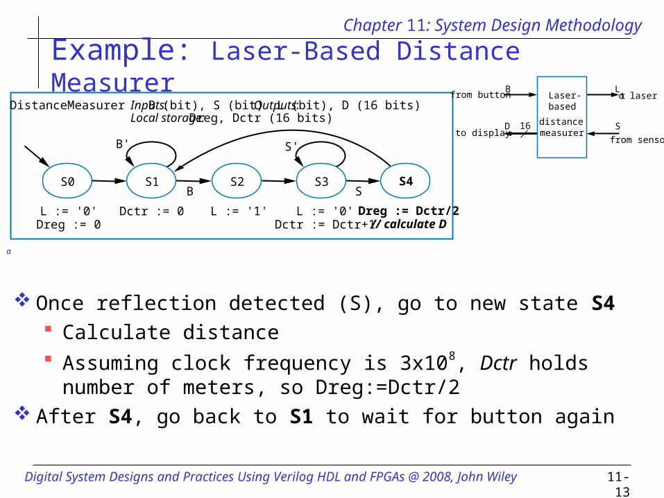
11-13Digital System Designs and Practices Using Verilog HDL and FPGAs @ 2008, John Wiley
Example: Laser-Based Distance Measurer
Once reflection detected (S), go to new state S4 Calculate distance Assuming clock frequency is 3x10⁸, Dctr holds number of
meters, so Dreg:=Dctr/2 After S4, go back to S1 to wait for button again
a
S0 S1 S2 S3
L := '0'Dreg := 0
L := '1' L := '0'Dctr := Dctr+1
Dreg := Dctr/2// calculate D
Dctr := 0
B' S'
B SS4
Inputs: B (bit), S (bit) Outputs: L (bit), D (16 bits)DistanceMeasurerLocal storage: Dreg, Dctr (16 bits)
Laser-based
distancemeasurer
16
from button
to displayS
L
D
Bto laser
from sensor

Chapter 11: System Design Methodology
11-14Digital System Designs and Practices Using Verilog HDL and FPGAs @ 2008, John Wiley
ASM Charts
ASM (algorithmic state machine) charts specify RTL operations on the per-cycle basis. show clearly the flow of control from state to state. are very suitable for data path-controller architectures.
An ASM chart is composed of State block Decision block Conditional output block
Chapter 11: System Design Methodology
11-15Digital System Designs and Practices Using Verilog HDL and FPGAs @ 2008, John Wiley
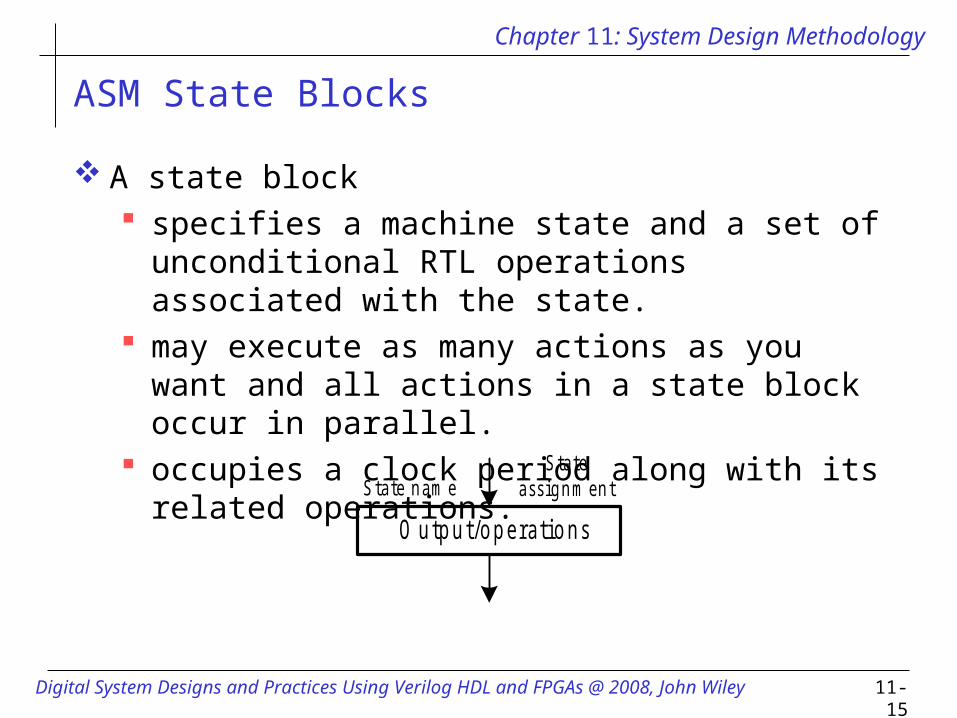
ASM State Blocks
A state block specifies a machine state and a set of unconditional RTL
operations associated with the state. may execute as many actions as you want and all actions
in a state block occur in parallel. occupies a clock period along with its related operations.
O u tp u t/o p e ra tio n s
S ta tea ssign m en tS ta te n am e
Chapter 11: System Design Methodology
11-16Digital System Designs and Practices Using Verilog HDL and FPGAs @ 2008, John Wiley
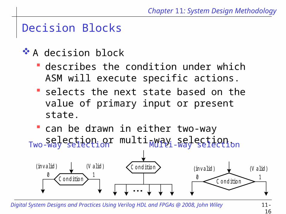
Decision Blocks
A decision block describes the condition under which ASM will execute
specific actions. selects the next state based on the value of primary input
or present state. can be drawn in either two-way selection or multi-way
selection.
Two-way selection Multi-way selection
C o n d itio n10
(V a lid )( in v a lid ) C o n d itio n
C o n d itio n10
(V a lid )( in v a lid )
Chapter 11: System Design Methodology
11-17Digital System Designs and Practices Using Verilog HDL and FPGAs @ 2008, John Wiley
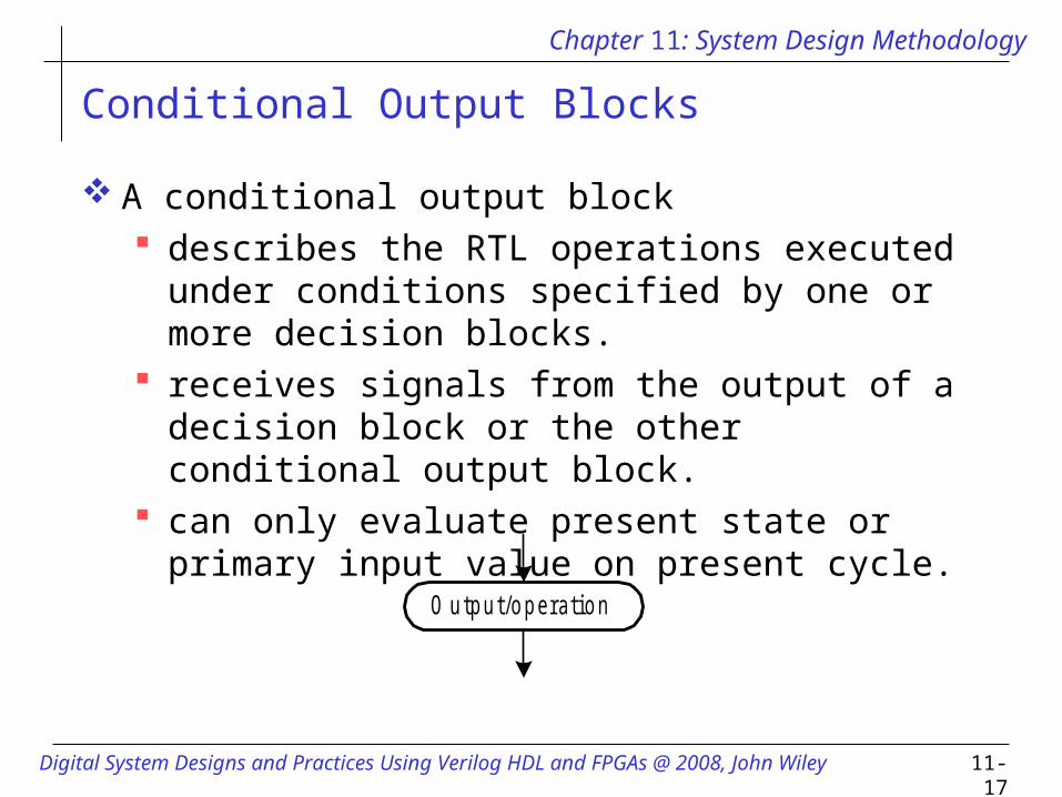
Conditional Output Blocks
A conditional output block describes the RTL operations executed under conditions
specified by one or more decision blocks. receives signals from the output of a decision block or the
other conditional output block. can only evaluate present state or primary input value on
present cycle.
O u tp u t/o p e ra tio n
Chapter 11: System Design Methodology
11-18Digital System Designs and Practices Using Verilog HDL and FPGAs @ 2008, John Wiley
ASM Blocks
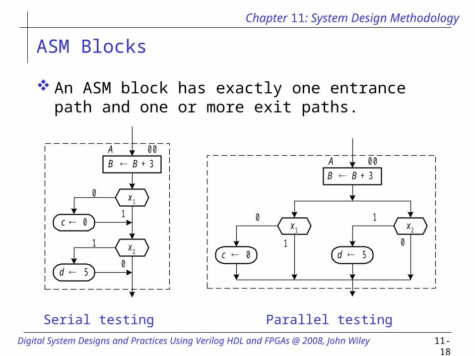
An ASM block has exactly one entrance path and one or more exit paths.
Serial testing Parallel testing
B
0 0A B + 3
x 1 x 2
c 0 d 5
0
1
1
0
B
x 1
1
0 0A
x 2
c
0
0
B + 3
d 5
1
0
Chapter 11: System Design Methodology
11-19Digital System Designs and Practices Using Verilog HDL and FPGAs @ 2008, John Wiley
ASM Charts --- ASM Blocks
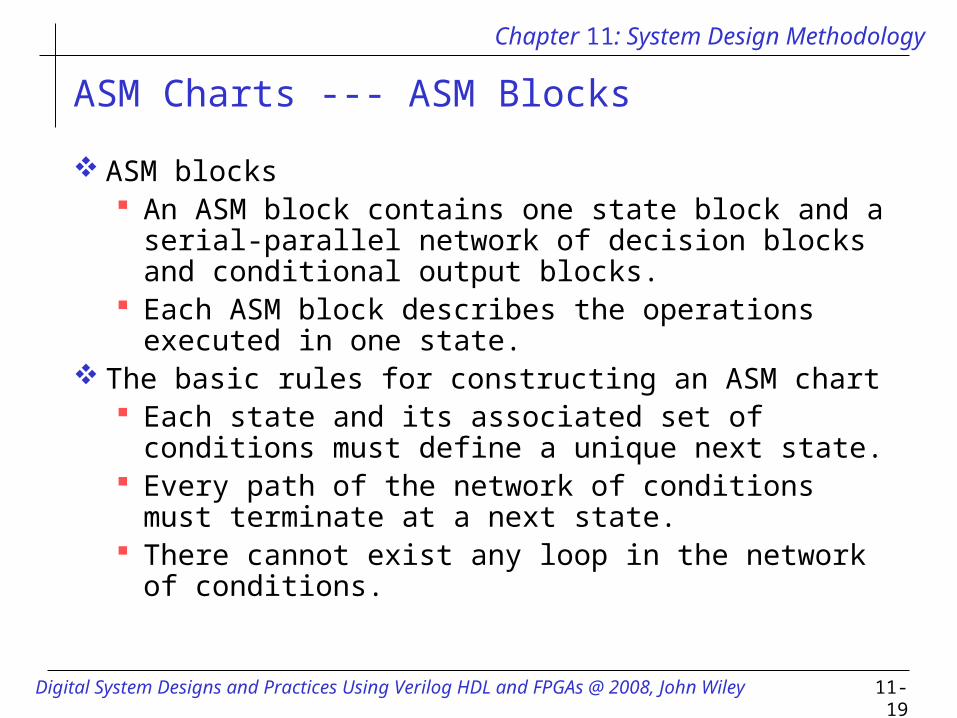
ASM blocks An ASM block contains one state block and a serial-
parallel network of decision blocks and conditional output blocks.
Each ASM block describes the operations executed in one state.
The basic rules for constructing an ASM chart Each state and its associated set of conditions must define
a unique next state. Every path of the network of conditions must terminate at
a next state. There cannot exist any loop in the network of conditions.
Chapter 11: System Design Methodology
11-20Digital System Designs and Practices Using Verilog HDL and FPGAs @ 2008, John Wiley
Invalid ASM Blocks
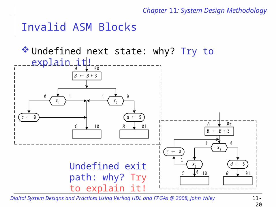
Undefined next state: why? Try to explain it!
Undefined exit path: why? Try to explain it!
B
0 0A B + 3
x 1
x 2c 0
d 5
0
1
1 0
0 1B1 0C
B
0 0A B + 3
x 1 x 2
c 0 d 5
0 1 1 0
0 1B1 0C
Chapter 11: System Design Methodology
11-21Digital System Designs and Practices Using Verilog HDL and FPGAs @ 2008, John Wiley
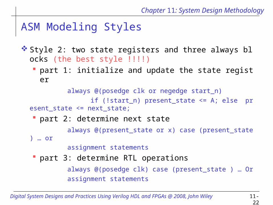
ASM Modeling Styles
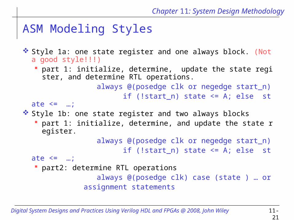
Style 1a: one state register and one always block. (Not a good style!!!) part 1: initialize, determine, update the state register, and deter
mine RTL operations. always @(posedge clk or negedge start_n) if (!start_n) state <= A; else state <= …; Style 1b: one state register and two always blocks
part 1: initialize, determine, and update the state register. always @(posedge clk or negedge start_n) if (!start_n) state <= A; else state <= …;
part2: determine RTL operations always @(posedge clk) case (state ) … or assignment statements
Chapter 11: System Design Methodology
11-22Digital System Designs and Practices Using Verilog HDL and FPGAs @ 2008, John Wiley
ASM Modeling Styles
Style 2: two state registers and three always blocks (the best style !!!!) part 1: initialize and update the state register
always @(posedge clk or negedge start_n)
if (!start_n) present_state <= A; else present_state <= next_state;
part 2: determine next state
always @(present_state or x) case (present_state ) … or
assignment statements
part 3: determine RTL operations
always @(posedge clk) case (present_state ) … Or
assignment statements

Chapter 11: System Design Methodology
11-23Digital System Designs and Practices Using Verilog HDL and FPGAs @ 2008, John Wiley
dp+cu Architecture Design
A digital system can be considered as a system composed of three major parts: data path performs all operations that are required in the
system. Memory temporarily stores the data used and generated
by data path unit. control unit controls and schedules all operations
performed by the data path unit.
c lk
D a ta o u tp u t
D a taR e a d /w r ite
D a ta p a th
C o n tro lle r
C o n tro l s ig n a ls S ta tu s
D a ta in p u t
M e m o ry
Chapter 11: System Design Methodology
11-24Digital System Designs and Practices Using Verilog HDL and FPGAs @ 2008, John Wiley
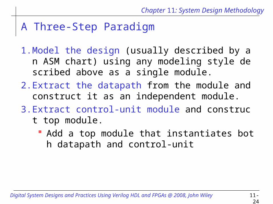
A Three-Step Paradigm
1. Model the design (usually described by an ASM chart) using any modeling style described above as a single module.
2. Extract the datapath from the module and construct it as an independent module.
3. Extract control-unit module and construct top module. Add a top module that instantiates both datapath and con
trol-unit
Chapter 11: System Design Methodology
11-25Digital System Designs and Practices Using Verilog HDL and FPGAs @ 2008, John Wiley
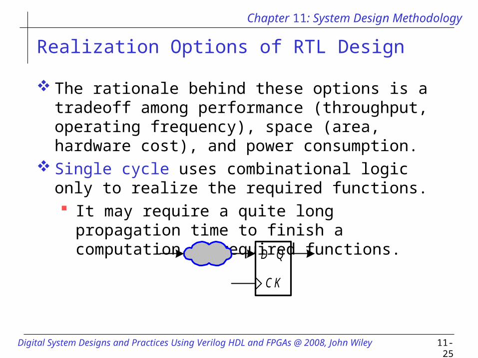
Realization Options of RTL Design
The rationale behind these options is a tradeoff among performance (throughput, operating frequency), space (area, hardware cost), and power consumption.
Single cycle uses combinational logic only to realize the required functions. It may require a quite long propagation time to finish a
computation of required functions.
D Q
C K
Chapter 11: System Design Methodology
11-26Digital System Designs and Practices Using Verilog HDL and FPGAs @ 2008, John Wiley
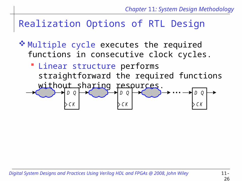
Realization Options of RTL Design
Multiple cycle executes the required functions in consecutive clock cycles. Linear structure performs straightforward the required
functions without sharing resources.
D Q
C K
D Q
C K
D Q
C K

Chapter 11: System Design Methodology
11-27Digital System Designs and Practices Using Verilog HDL and FPGAs @ 2008, John Wiley
Realization Options of RTL Design
Nonlinear (feedback or feed-forward) structure performs the required functions with sharing resources by using feedback or feed-forward connection.
D Q
C K
D Q
C K
D Q
C K
D Q
C K
Single-stage nonlinear structure
Multiple-stage nonlinear structure
Chapter 11: System Design Methodology
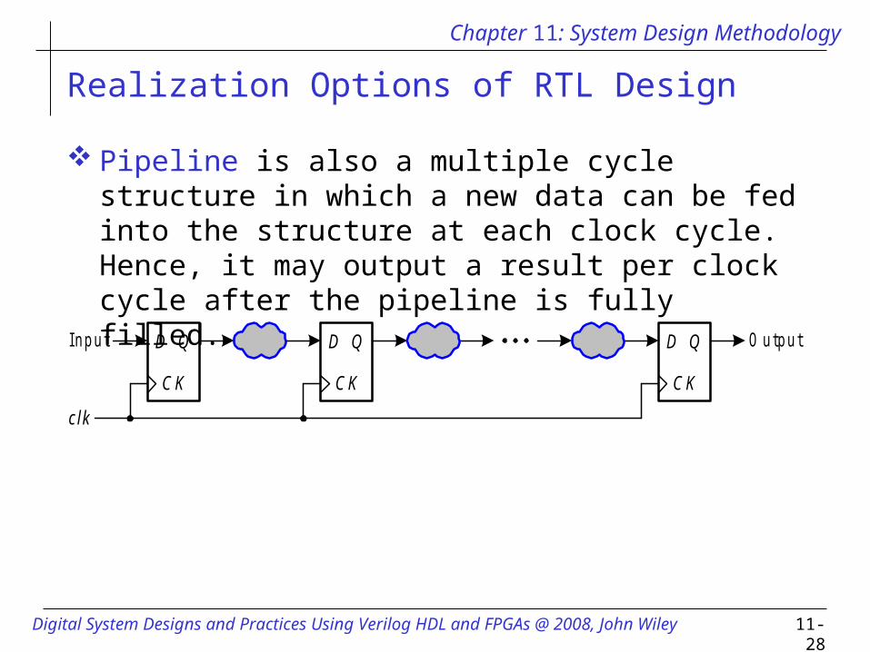
11-28Digital System Designs and Practices Using Verilog HDL and FPGAs @ 2008, John Wiley
Realization Options of RTL Design
Pipeline is also a multiple cycle structure in which a new data can be fed into the structure at each clock cycle. Hence, it may output a result per clock cycle after the pipeline is fully filled.
c lk
In p u t O u tp u tD Q
C K
D Q
C K
D Q
C K
Chapter 11: System Design Methodology
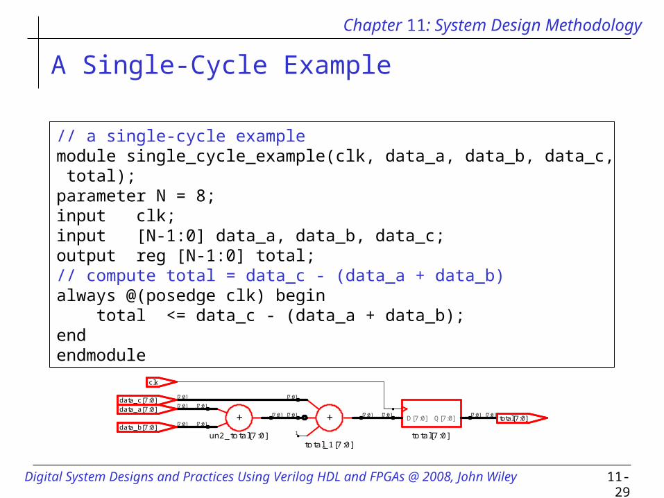
11-29Digital System Designs and Practices Using Verilog HDL and FPGAs @ 2008, John Wiley
A Single-Cycle Example
un2_total[7:0]
+
total_1[7:0]
+ total[7:0]
[7:0]
[7:0]
[7:0]
[7:0]
[7:0][7:0]
1
[7:0]Q[7:0][7:0] D[7:0] total[7:0][7:0]
data_c[7:0] [7:0]
data_b[7:0] [7:0]
data_a[7:0] [7:0]
clk
// a single-cycle examplemodule single_cycle_example(clk, data_a, data_b, data_c, total);parameter N = 8;input clk;input [N-1:0] data_a, data_b, data_c;output reg [N-1:0] total;// compute total = data_c - (data_a + data_b)always @(posedge clk) begin total <= data_c - (data_a + data_b); endendmodule
Chapter 11: System Design Methodology
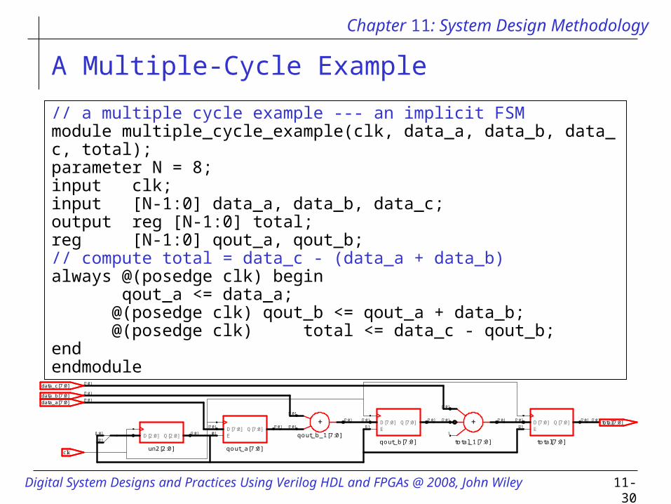
11-30Digital System Designs and Practices Using Verilog HDL and FPGAs @ 2008, John Wiley
A Multiple-Cycle Example
[1:0]
[2]
un2[2:0] qout_a[7:0]
qout_b_1[7:0]
+
qout_b[7:0] total_1[7:0]
+
total[7:0] [2:0]Q[2:0]D[2:0]
[7:0]Q[7:0][7:0] D[7:0][0] E
[7:0]
[7:0]
[7:0]
[7:0]Q[7:0][7:0] D[7:0][1] E
[7:0]
[7:0][7:0]
1
[7:0]Q[7:0][7:0] D[7:0][2] E
total[7:0][7:0]
data_c[7:0] [7:0]
data_b[7:0] [7:0]
data_a[7:0] [7:0]
clk
// a multiple cycle example --- an implicit FSMmodule multiple_cycle_example(clk, data_a, data_b, data_c, total);parameter N = 8;input clk;input [N-1:0] data_a, data_b, data_c;output reg [N-1:0] total;reg [N-1:0] qout_a, qout_b;// compute total = data_c - (data_a + data_b)always @(posedge clk) begin qout_a <= data_a; @(posedge clk) qout_b <= qout_a + data_b; @(posedge clk) total <= data_c - qout_b;endendmodule
Chapter 11: System Design Methodology
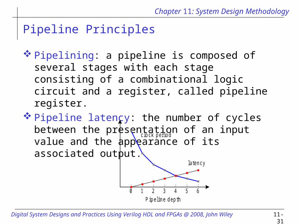
11-31Digital System Designs and Practices Using Verilog HDL and FPGAs @ 2008, John Wiley
Pipeline Principles
Pipelining: a pipeline is composed of several stages with each stage consisting of a combinational logic circuit and a register, called pipeline register.
Pipeline latency: the number of cycles between the presentation of an input value and the appearance of its associated output.
P ip e lin e d e p th0 5 64321
c lo c k p e r io d
la te n c y
Chapter 11: System Design Methodology
11-32Digital System Designs and Practices Using Verilog HDL and FPGAs @ 2008, John Wiley
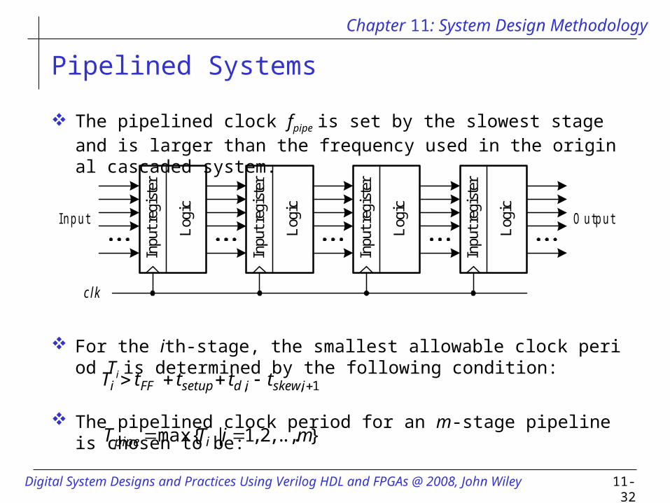
Pipelined Systems
The pipelined clock fpipe is set by the slowest stage and is larger than the frequency used in the original cascaded system.
For the ith-stage, the smallest allowable clock period Ti is determined by the following condition:
The pipelined clock period for an m-stage pipeline is chosen to be:
c lk
In p u t O u tp u t
Inpu
t reg
iste
r
Log
ic
Inpu
t reg
iste
r
Log
ic
Inpu
t reg
iste
r
Log
ic
Inpu
t reg
iste
r
Log
ic
1,, iskewidsetupFFi ttttT
} ,... ,2 ,1|max{ miTT ipipe
Chapter 11: System Design Methodology
11-33Digital System Designs and Practices Using Verilog HDL and FPGAs @ 2008, John Wiley
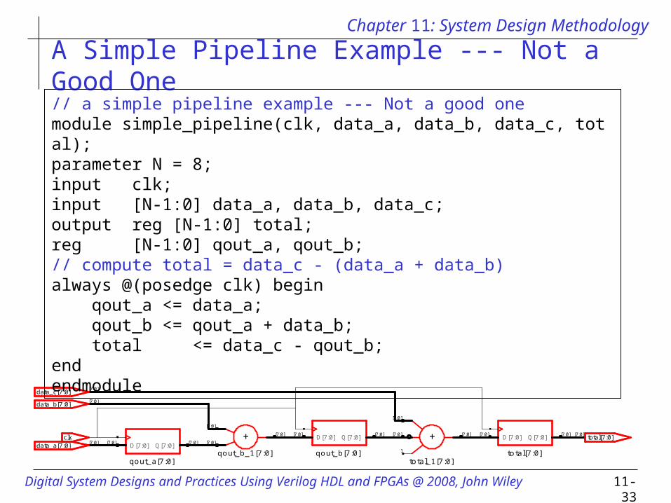
A Simple Pipeline Example --- Not a Good One
qout_a[7:0] qout_b_1[7:0]
+ qout_b[7:0]
total_1[7:0]
+ total[7:0]
[7:0]Q[7:0][7:0] D[7:0]
[7:0]
[7:0]
[7:0]
[7:0]Q[7:0][7:0] D[7:0]
[7:0]
[7:0][7:0]
1
[7:0]Q[7:0][7:0] D[7:0] total[7:0][7:0]
data_c[7:0] [7:0]
data_b[7:0] [7:0]
data_a[7:0] [7:0]clk
// a simple pipeline example --- Not a good onemodule simple_pipeline(clk, data_a, data_b, data_c, total);parameter N = 8;input clk;input [N-1:0] data_a, data_b, data_c;output reg [N-1:0] total;reg [N-1:0] qout_a, qout_b;// compute total = data_c - (data_a + data_b)always @(posedge clk) begin qout_a <= data_a; qout_b <= qout_a + data_b; total <= data_c - qout_b;endendmodule
Chapter 11: System Design Methodology
11-34Digital System Designs and Practices Using Verilog HDL and FPGAs @ 2008, John Wiley
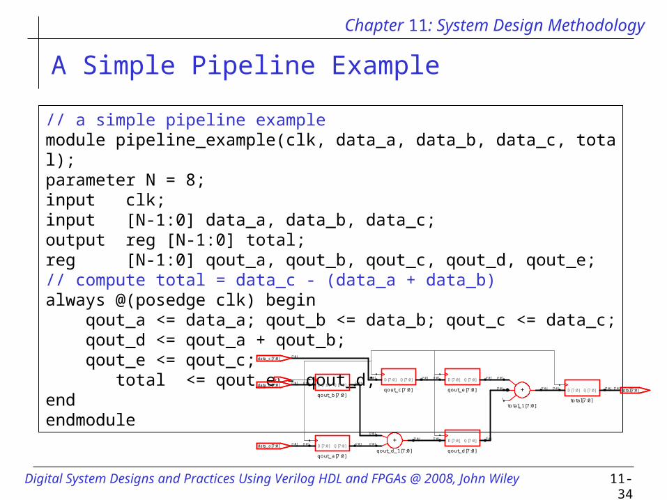
A Simple Pipeline Example
// a simple pipeline examplemodule pipeline_example(clk, data_a, data_b, data_c, total);parameter N = 8;input clk;input [N-1:0] data_a, data_b, data_c;output reg [N-1:0] total;reg [N-1:0] qout_a, qout_b, qout_c, qout_d, qout_e;// compute total = data_c - (data_a + data_b)always @(posedge clk) begin qout_a <= data_a; qout_b <= data_b; qout_c <= data_c; qout_d <= qout_a + qout_b; qout_e <= qout_c; total <= qout_e - qout_d;endendmodule
qout_a[7:0]
qout_b[7:0] qout_c[7:0] qout_e[7:0]
qout_d_1[7:0]
+ qout_d[7:0]
total_1[7:0]
+ total[7:0]
[7:0]Q[7:0][7:0] D[7:0]
[7:0]Q[7:0][7:0] D[7:0]
[7:0]Q[7:0][7:0] D[7:0] [7:0]Q[7:0][7:0] D[7:0]
[7:0]
[7:0]
[7:0]
[7:0]Q[7:0][7:0] D[7:0]
[7:0]
[7:0][7:0]
1
[7:0]Q[7:0][7:0] D[7:0] total[7:0][7:0]
data_c[7:0] [7:0]
data_b[7:0] [7:0]
data_a[7:0] [7:0]
clk