chapter 11: foundations of combinational circuits guy...
TRANSCRIPT
Digital Logic Design: a rigorous approach c©Chapter 11: Foundations of combinational circuits
Guy Even Moti Medina
School of Electrical Engineering Tel-Aviv Univ.
November 23, 2015
Book Homepage:http://www.eng.tau.ac.il/~guy/Even-Medina
1 / 61

Combinational Circuit
Representation of Boolean functions:
Truth tables can be implemented by a ROM (e.g., lookuptables, FPGAs)
SOP Boolean formulas can be implemented by PLA circuits.
Boolean formulas can be implemented by rooted trees withcombinational gates.
The general case: combinational circuits - topic of thischapter!
2 / 61
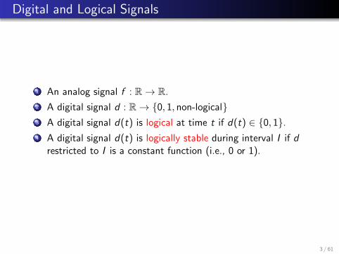
Digital and Logical Signals
1 An analog signal f : R→ R.
2 A digital signal d : R→ {0, 1, non-logical}
3 A digital signal d(t) is logical at time t if d(t) ∈ {0, 1}.
4 A digital signal d(t) is logically stable during interval I if drestricted to I is a constant function (i.e., 0 or 1).
3 / 61

Digital Approach to Combinational Circuits
interested only in value(output) when the inputs are logical.
logical inputs imply logical outputs (eventually).
how long does it take?
4 / 61

Digital view of combinational circuits
Setting and notation:
Combinational gate g
Inputs: x1 and x2Output: y .
We refer only to digital signals.
Terminal means input or output.
Digital signal at terminal z is denoted by z(t).
Our goals are to:
specify the functionality of combinational gate g by a Booleanfunction,
define when a combinational gate g is consistent, and
define the propagation delay of g .
5 / 61
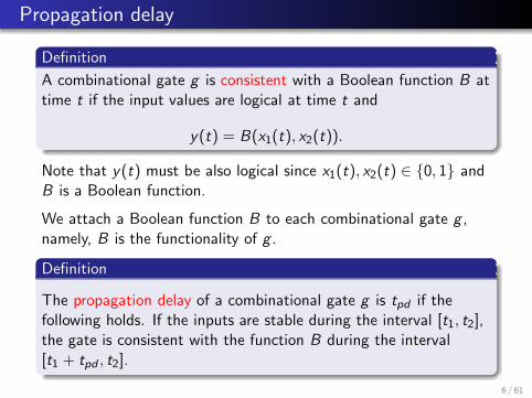
Propagation delay
Definition
A combinational gate g is consistent with a Boolean function B attime t if the input values are logical at time t and
y(t) = B(x1(t), x2(t)).
Note that y(t) must be also logical since x1(t), x2(t) ∈ {0, 1} andB is a Boolean function.
We attach a Boolean function B to each combinational gate g ,namely, B is the functionality of g .
Definition
The propagation delay of a combinational gate g is tpd if thefollowing holds. If the inputs are stable during the interval [t1, t2],the gate is consistent with the function B during the interval[t1 + tpd , t2].
6 / 61

Propagation delay - remarks
What if t2 < t1 + tpd? Periods of steady state must be longerthan the propagation delays. Otherwise, the combinationalgate may not reach consistency.
tpd is an upper bound on the amount of time that elapses tilla combinational gate becomes consistent (provided that itsinputs are stable). The actual time depends on:
x(t) during the interval (−∞, t) (i.e., how fast does the inputchange?),noise, andmanufacturing variance.
pessimistic assumptions should not render a circuit incorrect(if t ′ ≥ tpd , then t ′ is also a prop. delay).
Timing analysis of circuits composed of many gates dependson the upper bounds we use; the tighter the bounds, the moreaccurate the timing analysis is.
7 / 61
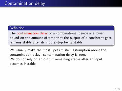
Contamination delay
Definition
The contamination delay of a combinational device is a lowerbound on the amount of time that the output of a consistent gateremains stable after its inputs stop being stable.
We usually make the most “pessimistic” assumption about thecontamination delay: contamination delay is zero.We do not rely on an output remaining stable after an inputbecomes instable.
8 / 61

propagation delay and contamination delay
The outputs become stable at most tpd time units after the inputsbecome stable. The outputs remain stable at least tcont time unitsafter the inputs become instable.
inputs
tpdoutputs
tcont
Figure: The x-axis corresponds to time. The red segments signify thatthe signal is not guaranteed to be logical; the green segments signify thatthe signal is guaranteed to be stable.
9 / 61

Example
Consider an and-gate with inputs x1(t) and x2(t) and an outputy(t). Suppose that the propagation delay of the gate is tpd = 2seconds. (All time units are in seconds in this example, so unitswill not be mentioned anymore in this example).
the inputs equal 1 during the interval [100, 109] . When is thegate consistent?
x1(t) = 1 during the interval (109, 115], x2(t) = non-logicalduring the interval (109, 110), and x2(t) = 0 during theinterval [110, 115]. What can we say about y(t)?
x2(t) remains stable during the interval [110, 120], x1(t)becomes non-logical during the interval (115, 116), and x1(t)equals 1 again during the interval [116, 120]. What can we sayabout y(t)?
10 / 61

and(0, non− logical) = 0?
We cannot determine that and(0, non − logical) = 0. This istechnology dependent. Our formalism does not imply this at all!For example, in a CMOS nand-gate, one can determine that theoutput is zero if one of the outputs is one (even if the other inputis non-logical).Another drawback of assuming that and(0, non − logical) = 0 isthat timing depends on the values of the signals (timing analysisbecomes a very hard computational problem). In particular,instead of a task that can be computed in linear time, timinganalysis (of general combinational circuits) becomes an NP-hardtask (i.e., a task that is unlikely to be solvable in polynomial time).
11 / 61

Building Blocks
The building blocks of combinational circuits:
Combinational gates (e.g., inverter, or-gate, nor-gate, etc.)
Wires and nets
12 / 61

combinational gates - terminology
The basic gates that we consider are: inverter (not-gate),or-gate, nor-gate, and-gate, nand-gate, xor-gate,nxor-gate, multiplexer (mux). All this gates have a singleoutput.
inputs and outputs of a gate are often referred to asterminals, ports, or even pins.
fan-in of a gate g = number of input terminals of g (i.e., thenumber of bits in the domain of the Boolean function thatspecifies the functionality of g).
basic gates have constant fan-in (2-3).
fan-out 6= the number of output ports.
13 / 61

combinational gates - terminology
{in(g)i}ni=1 = the input ports of a gate g , where n
=fan-in(g).
{out(g)i}ki=1 = the output ports of a gate g , where
k=number of output ports of g .
terminals(g)△
= {in(g)i}in(g)i=1 ∪ {out(g)i}
out(g)i=1 .
14 / 61

Input/Output gates
Definition (input and output gates)
An input gate is a gate with zero inputs and a single output. Anoutput gate is a gate with one input and zero outputs.
Output GateInput Gate
Inputs from the “external world” are fed to a circuit via inputgates.
Outputs to the “external world” are fed by the circuit viaoutput gates.
an input gate is labeled (in, xi), where xi is the name of thesignal along the wire that emanates from it.
an output gate is labeled (out, yi ), where yi is the name ofthe signal along the wire that enters it.
15 / 61

Wires and nets
A wire is a connection between two terminals (e.g., an output ofone gate and an input of another gate). In the zero-noise model,the signals at both ends of a wire are identical.Very often we need to connect several terminals (i.e., inputs andoutputs of gates) together. We could, of course, use any set ofedges (i.e., wires) that connects these terminals together. Insteadof specifying how the terminals are physically connected together,we use nets.
Definition
A net is a subset of terminals that are connected by wires. Thefan-out of a net N is the number of input terminals that arecontained in N.
16 / 61
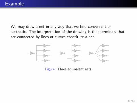
Example
We may draw a net in any way that we find convenient oraesthetic. The interpretation of the drawing is that terminals thatare connected by lines or curves constitute a net.
Figure: Three equivalent nets.
17 / 61
Digital Signal in A Net
How do we define the digital signal N(t) for the whole net?
Many terminals, perhaps far away, why should they “agree”?
We solve this problem by defining N(t) as logical only if thereis a consensus among all the digital interpretations of theanalog signals at all the terminals of the net.
If there is no consensus, then N(t) is non-logical.
18 / 61

Direction in nets
We say that a net N feeds an input terminal t if the input terminalt is in N.We say that a net N is fed by an output terminal t if t is in N.Direction of signals along nets is obtained in “pure” CMOS gatesas follows. Output terminals are connected (via low resistance) tothe ground or to the power (but not both!). Input terminals, onthe other hand, are connected only to capacitors.
G
a net fed by Ga net that feeds G
19 / 61

Simple nets
Definition
A net N is simple if (i) N is fed by exactly one output terminal,and (ii) N feeds at least one input terminal.
Consider a simple net N = {t, t1, t2, . . . , tk}, where:
t is an output terminal
each ti is an input terminal.
The simple net N can be modeled by a “star” of edges (or wires):
t → t1, t → t2, . . . , t → tk
(Directed edges because information flows in one direction.)
take home message
Simple nets make life simpler...
20 / 61

full specification of a wire
A full description of a wire is of the form
(g1, t) −→ (g2, t′),
where
t is an output terminal of gate g1, and
t ′ is an input terminal of gate g2.
21 / 61

Wire notation
Often, we abbreviate and describe the wire (g1, t1) −→ (g2, t2) byg1 −→ g2. This abbreviation is not ambiguous if the followingholds:
The gate g1 has a single output terminal. Since there is onlyone output terminal, we need not specify to which outputterminal the wire is connected.
(i) Only two wires are directed toward g2, (ii) g2 has twoinput terminals, and (iii) the Boolean function of g2 iscommutative. In this case, we connect each wire to a differentinput terminal.
22 / 61

Library of gates
Let Γ denote a library of combinational gates that containsstandard combinational gates such as an inverter, or-gate,and-gate, et cetera.The library Γ contains a sub-library IO that contains two specialtypes of gates: input-gates (in, xi ) and output-gates (out, yj).
23 / 61

How to define a combinational circuit? (1)
Suppose we want to design a circuit that contains two and gates,three inputs, x1, x2, x3, and two outputs y1, y2, wherey1 = and(x1, x2) and y2 = and(x2, x3). One way to describe thecircuit is to draw a schematic. We would like to describe thecircuit formally (a schematic is perhaps easy to “read”, but hard toargue about).
(in, x3)
(in, x1)
(in, x2)
(out, y1)
(out, y2)
and
and
Figure: A combinational circuit.
24 / 61

How to define a combinational circuit? (2)
(in, x3)
(in, x1)
(in, x2)
(out, y1)
(out, y2)
and
and
We define a set V△
= {vi}7i=1 of nodes. Now, we need to assign a
gate type to each node. We do this by defining a functionπ : V → Γ.
π(v1) = (in, x1), π(v2) = (in, x2), π(v3) = (in, x3),
π(v4) = π(v5) = and,
π(v6) = (out, y1), π(v7) = (out, y2).
25 / 61

How to name terminals?
(in, x3)
(in, x1)
(in, x2)
(out, y1)
(out, y2)
and
and
Both v4 and v5 are assigned and-gates.
How can we distinguish between the input ports of v4 and theinput ports of v5?
An and-gate has two input ports, called in(and)1 andin(and)2, and one output terminal called out(and).
Use “family” names to terminals. For example, the first inputport of v4 is called (v4, in(and)1). This is a bit cumbersomebut unambiguous.
26 / 61

How to name terminals?
(in, x3)
(in, x1)
(in, x2)
(out, y1)
(out, y2)
and
and
In the case of input and output gates, we abbreviate.
Write (in, xi ), instead of, out((in, xi )).
Similarly, we write (out, yj), instead of, in((out, yj )).
27 / 61

Definition of Terminals
Consider a set of nodes V and a function π : V → Γ assigns a gatetype to each node.
Definition
The set of terminals of V with respect to π is defined as follows
terminals(V , π)△
= {(v , t) : v ∈ V , t ∈ terminals(π(v))}.
28 / 61

Netlist
A netlist is a way to describe how gates are connected to eachother.
Definition
A netlist is a tuple H = (V ,N, π), where V is a set of nodes,π : V → Γ assigns a gate type to each node, and N is a set of netsover terminals(V , π). We require that the nets in N are pairwisedisjoint.
29 / 61

Netlist
(in, x3)
(in, x1)
(in, x2)
(out, y1)
(out, y2)
and
and
The set N of nets consists of the following nets.
{(v1, (in, x1)), (v4, in(and)1)} ,
{(v2, (in, x2)), (v4, in(and)2), (v5, in(and)1)} ,
{(v3, (in, x3)), (v5, in(and)2)} ,
{(v4, out(and)), (v6, (out, y1))} ,
{(v5, out(and)), (v7, (out, y2))} .
30 / 61

Graph Representation of a Netlist with Simple Nets
A netlist H = (V ,N, π) in which all nets are simple can berepresented by a directed graph DG (H) = (V , N).
For each net n = {t, t1, . . . , tk} with an output terminal t andinput terminals t1, . . . , tk . Suppose that t is a terminal ofnode v , and ti is a terminal of node vi .
This net n is represented in N by the set of directed edges{(v , vi )}
ki=1.
31 / 61

Graph Representation of a Netlist with Simple Nets
(in, x3)
(in, x1)
(in, x2)
(out, y1)
(out, y2)
and
and
Set V = {v1, . . . , v7} and
N = {(v1, v4), (v2, v4), (v2, v5), (v3, v5), (v4, v6), (v5, v7)} .
32 / 61

Graph representation of a netlist
DG (H) may have directed edges of the form (v , v); suchedges are called self-loops. Self-loops can be obtained bygates that their output is connected to their input.
DG (H) may have parallel edges.
33 / 61

Definition of Combinational Circuits.
Definition
A netlist H = (V ,N, π) is a combinational circuit if it satisfies thefollowing conditions.
1 Every net in N is simple.
2 Every terminal in terminals(V , π) belongs to exactly one netin N.
3 The directed graph DG (H) is acyclic.
Question
Can you check if a netlist is a combinational circuit?
34 / 61

Gate Symbols
Instead of writing the label π(v) in the vertex v , one sometimesdepicts the vertex by a symbol that represents π(v).
XOR−gate OR−gate NOR−gate
inverter AND−gate NAND−gate
35 / 61

Example : Half Adder
The combinational circuit C = (G , π) is called a Half-Adder.
(in, b)
(in, a)
(out, s)
(out, cout) v1
v2
v3
v4
v5
v6
Figure: A Half-Adder combinational circuit and its matching DAG.
The set of the combinational gates in this example isΓ = {and,xor}. The labeling function π : V → Γ ∪ IO is asfollows.
π(1) = (in, a), π(2) = (in, b),
π(3) = and, π(4) = xor,
π(5) = (out, cout), π(6) = (out, s) .
36 / 61

Bad Circuits
Can you explain why these are not valid combinational circuits?
Figure: Two examples of non-combinational circuits.
37 / 61

Important properties of combinational circuits
Completeness: For every Boolean function B , there exists acombinational circuit that implements B .
Soundness: Every combinational circuit implements a Booleanfunction.
Simulation: Given the digital values of the inputs of acombinational circuit, one can simulate the circuitefficiently (the running time is linear in the size ofthe circuit). Namely, one can compute the digitalvalues of the outputs of the circuit that are output bythe circuit once the circuit becomes consistent.
Delay analysis: Given the propagation delays of all the gates in acombinational circuit, one can compute in linear timean upper bound on the propagation delay of thecircuit.
38 / 61

Plan
algorithm for simulation and delay analysis.
algorithm implies soundness.
prove completeness by implementing Boolean formulas.
39 / 61
Assumptions
To simplify matters, assume that every combinational gate:
has a single output terminal
has at most two input terminals (fan-in ≤ 2)
implements a commutative Boolean function.
Reason: port information of each wire can be easily deduced...
40 / 61

Notation
Consider a combinational circuit C = (G , π).
We identify a vertex v with its output terminal, and denotethe digital signal at the output terminal of v simply by v(t).
For an output-gate v , we denote the digital signal at the inputterminal of v also by v(t).
We assume that C has k input gates named them x1, . . . , xk .
To simplify notation, we use ~x(t) to denote the vectorx1(t), . . . , xk(t).
41 / 61

Simulation theorem of combinational circuits
Theorem
Assume that the digital signals {xi (t)}ki=1 are stable during the
interval [t1, t2]. Then, for every vertex v ∈ V there exist:
1 a Boolean function fv : {0, 1}k → {0, 1}, and
2 a propagation delay tpd (v)
such that v(t) = fv (~x(t)), for every t ∈ [t1 + tpd (v), t2].
Note that tpd (v) 6= tpd (π(v)). The propagation delay tpd (π(v))refers to the delay of a single gate of type π(v). This delay ismeasured with respect to the input of the gate. On the otherhand, the propagation delay tpd (v) refers to the delay of theoutput of v with respect to the input gates of the circuit C .
42 / 61

Proof by Algorithm
Simulation algorithm:
Similar to EVAL algorithm.
Sorts vertices in topological order.
Given ~x evaluates value of every output terminal (andtherefore, wire).
Computes accumulated delay along longest paths.
43 / 61

Algorithm 1 SIM(C , ~x) - An algorithm for simulating the combina-tional circuit C = (G , π) with respect an input vector ~x .
(v1, v2, . . . , vn)← TS(G ) {topological sorting of G}
For i = 1 to n doswitch degin(vi )
case degin(vi ) = 0: {π(vi ) = (in, xj)}
Set fvi (~x)△
= xj and tpd(vi )△
= 0.

Algorithm 2 SIM(C , ~x) - An algorithm for simulating the combina-tional circuit C = (G , π) with respect an input vector ~x .
(v1, v2, . . . , vn)← TS(G ) {topological sorting of G}
For i = 1 to n doswitch degin(vi )
case degin(vi ) = 1:If {π(vi ) = not}, then
Let vj −→ vi denote the arc that enters vi .Set fvi (~x) = not(fvj (~x)) andtpd(vi ) = tpd(vj ) + tpd(not).
If {π(vi ) = (out, y)}, then
Let vj −→ vi denote the arc that enters vi .Set fvi (~x) = fvj (~x) and tpd(vi ) = tpd(vj).

Algorithm 3 SIM(C , ~x) - An algorithm for simulating the combina-tional circuit C = (G , π) with respect an input vector ~x .
(v1, v2, . . . , vn)← TS(G ) {topological sorting of G}
For i = 1 to n doswitch degin(vi )
case degin(vi ) = 2:
Let vj −→ vi and vk −→ vi denote the arcs thatenter vi .Set fvi (~x) = B
π(vi )(fvj (~x), fvk (~x)), andtpd(vi ) = max{tpd(vj), tpd(vk )}+ tpd(π(vi )).

Algorithm Correctness
∀i ∈ [1..n] ∀~x ∈ {0, 1}k ∀t ∈ [t1 + tpd (vi), t2] : vi(t) = fvi (~x).
The proof is by complete induction on i , the index of a vertex aftertopological sorting takes place.
induction basis: v1 is a source, and hence π(v1) = (in, xj).
induction step: three cases...
47 / 61

Multiple topological orderings?!
Recall that a DAG may have more than one topological ordering.
Lemma
The output of SIM(C , ~x) does not depend on the topological
ordering computed by TS(G ).
48 / 61

Soundness
The simulation Theorem enables us to regard a combinationalcircuit as a “macro-gate”.
This macro-gate computes a Boolean functionB : {0, 1}k → {0, 1}ℓ, where k denotes the number of inputgates and ℓ denotes the number of output gates.
All instances of the same combinational circuit implement thesame Boolean function and have the same propagation delay.
Corollary (Soundness)
Every combinational circuit implements a Boolean function.
49 / 61

Remarks
Simulation algorithm generalizes EVAL from trees to DAGs.
The computation of the propagation delays is, in fact, acomputation of longest paths in DAGs with non-unit delaysδ : V → R
≥0.
Algorithm 4 weighted-longest-path-lengths(V ,E , δ) - An algorithmfor computing the longest delays of paths in a DAG. Returns a delayfunction d(v).
1 topological sort: (v0, . . . , vn−1)← TS(V ,E ).2 For j = 0 to (n − 1) do
1 If vj is a source then d(vj)← δ(vj).2 Else
d(vj ) = δ(vj) + max{
d(vi ) | i < j and (vi , vj) ∈ E}
.
50 / 61

What about constant inputs?
We do not rule out the usage of constants as inputs.
In this case we add the possibility for input-gates labeled(in, 0) and (in, 1). Such an input gate feeds a constant to thecircuit.
Algorithm SIM needs to be modified to handle constantinputs. Namely, the case that vi is a source has to be split toa constant input and a variable input.
51 / 61

Completeness
Want to prove that every Boolean function can beimplemented by a combinational circuit.
{¬,or,and} is a complete set of logical connectives.
Given a Boolean function B : {0, 1}n → {0, 1}, represent it bya Boolean formula ϕ.
We need to show how to implement ϕ by a combinationalcircuit.
52 / 61

From formulas to circuits
Demonstrate by example (full proof in book).
X1X1 X2
or
and
not
and
X1 X2 X1
notor
or
and
(in, X1) (in, X2)
(out, y)
not
Figure: (a) the parse tree of ϕ, (G , π), (b) merge sources labeled bysame variable, (c) combinational circuit that implements ϕ.
53 / 61
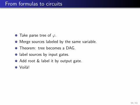
From formulas to circuits
Take parse tree of ϕ.
Merge sources labeled by the same variable.
Theorem: tree becomes a DAG.
label sources by input gates.
Add root & label it by output gate.
Voila!
54 / 61

Cost
Let C = (G , π) denote a combinational circuit whereG = (V ,E ) is a directed graph and π : V → Γ ∪ IO is alabeling.
Let c : Γ ∪ IO → R≥0 denote a cost function. Usually,
input-gates and output-gates have zero cost.
Definition
The cost of C is defined by
c(C )△
=∑
v∈V
c(π(v)).
55 / 61

Propagation delay
The propagation delays tpd (v) are computed by AlgorithmSIM(C , ~x).
Definition
The propagation delay of C is defined by
tpd (C )△
= maxv∈V
tpd (v).
We often refer to the propagation delay of a combinational circuitas its depth or simply its delay.
Definition
The propagation delay of a path p in G is defined as
tpd (p)△
=∑
v∈p
tpd (π(v)).
56 / 61

Critical paths
Algorithm SIM(C , ~x) computes the largest delay of a path in G .
Claim
tpd (C ) = max {tpd (p) | p is a path in G}
Definition
Let G = (G , π) denote a combinational circuit. A path p in G iscritical if tpd (p) = tpd (C ).
We focus on critical paths that are maximal (i.e., cannot be furtheraugmented). This means that maximal critical paths begin in aninput-gate and end in an output-gate.
57 / 61

Semantics and Syntax
semantics - the function that a circuit implements(functionality, behavior). In non-combinational circuits, theoutput depends not only on the current inputs, so semanticscannot be described simply by a Boolean function.
syntax - a formal set of rules that govern how “grammaticallycorrect” circuits are constructed from smaller circuits (just assentences are built by combining words).
the functionality (or gate-type) of each gate is not important.rules for connecting gates together must be followed.syntax does not guarantee that the resulting circuit is useful.syntax is a restriction that brings many benefits: well definedfunctionality, simple simulation, and simple timing analysis.
58 / 61

Design Rules
In this chapter we defined design rules for building combinationalcircuits. These design rules define syntactically correct circuits.Our main result is that syntactically correct circuits, calledcombinational circuits, can implement any Boolean function.
We are now left with the following design task: Given a Booleanfunction B , design a combinational circuit C that implements Bsuch that the delay and cost of C is as small as possible.
59 / 61

Summary
Combinational circuits: formal definition.
Bottom-up approach: basic building blocks: gates and wires.Each gate has a simple specification: functionality and tpd .
Syntactic definition of combinational circuits: only depends onthe topology of the circuit, namely, how the terminals of thegates are connected.One can check in linear time whether a given circuit is indeeda combinational circuit.
Easy simulation: one can compute in linear time the digitalsignals of every wire in the circuit. Moreover, one can alsocompute in linear time the propagation delay of every wire.
Two quality measures: cost and propagation delay. The costof a combinational circuit is the sum of the costs of the gatesin the circuit. The propagation delay of a combinational is themaximum delay of a path in the circuit.
60 / 61