challenges of contacting lead-free devices
TRANSCRIPT

Challenges of Contacting Lead-Free Devices
2005 Burn-in and Test Socket WorkshopMarch 6 - 9, 2005
Burn-in & TestSocket
Workshop
TM
Brian William Sheposh Johnstech International

Challenges of Contacting Lead-Free Devices 2
Discussion Topics
• Defining Interconnect Success• Lead-free Material Trends and
Applications• Specifics of Lead-Free Alloys• The Impact on Interconnect Success• Conclusion: Achieving Interconnect
Success

Challenges of Contacting Lead-Free Devices 3
Interconnect Success
• Goal: Minimize and sustain the junction resistance between the device lead and contact.
Rtotal = Rc + Rfilm
ConstrictionRc ∝ F-1/2 (force) ; Rc ∝ ρtip (plating)
FilmRfilm >> RC (oxide, debris)

Challenges of Contacting Lead-Free Devices 4
Challenges to Interconnect Success
• Maintaining bias throughout product life.
• Rfilm develops on the surface of the contact over insertion (debris and oxide).
• Wear of the contact tip can compromise the interconnect integrity:– Plating (contact under-plate metallic oxidizes)– Function (wipe, piercing, etc.)
Rc ∝ F-1/2
Rfilm >> RC
Rc ∝
ρtip
Rc ∝ F-1/2

Challenges of Contacting Lead-Free Devices 5
Industry Lead-Free Trends
• Leaded and Pad Packages– Matte Sn– NiPd ; NiPdAu– SnBi– Au
• Ball Grid Array Packages (BGA)– SnAg3.0-4.0Cu0.5

Challenges of Contacting Lead-Free Devices 6
Challenges in the Field• Matte Sn
– Customers see faster rise in resistance which leads to more frequent cleaning when compared to SnPb.
– Reduced contact life has been observed vs. SnPb, but not as great as with NiPdAu.
• NiPdAu– Customers observe good contact resistance until
the contact plating wears, which promotes a drastic drop in 1st pass yields.
– Contact life is much less when testing NiPdAu vs. Sn Pb.

Challenges of Contacting Lead-Free Devices 7
Qualification of Interconnect Success
• Contactor Designs• BGA Contactor
– Sn63Pb37 eutectic – Sn95.5Ag4.0Cu0.5
• Pad Contactor : ROL200 Design– Sn90Pb10
– Matte Sn100
– NiPdAu

Challenges of Contacting Lead-Free Devices 8
Qualification of Interconnect Success
• Contacts were populated into a contactor and mounted to a test board.
• Force Testing: Contact force was measured in real-time as devices were inserted into the contactor.
• Resistance Testing: The test board and devices were designed so that four-point Kelvin resistance measurements were made across pairs of contacts throughout the contactor.

Challenges of Contacting Lead-Free Devices 9
Qualification of Interconnect Success
• Resistance Testing cont.: Packaged devices were cycled through the contactor and Kelvin resistance measurements were recorded:– BGA Devices: Each device was cycled ten times
with resistance readings at the first and sixth insertion (reduce cost)
– Pad Devices: Each device was cycled only once, insuring virgin plating material on each insertion.

Challenges of Contacting Lead-Free Devices 10
SnAgCu BallsPhysical Appearance
• A dull, grainy, matte finish on the SnAgCu balls due to the formation of pure Sn dendrites on the surface of the ball.
SnPb SnAgCu200 µm 100 µm

Challenges of Contacting Lead-Free Devices 11
EDS Spectrum of Dendrite Rich Regions - SnAgCu Balls
Average composition in non-dendritic regionSn 96.1%Cu 2.3%Ag 1.6%
Average composition in dendritic rich regionSn 99.8%Cu 0.2%Ag <0.1%
100 µm
20 µm

Challenges of Contacting Lead-Free Devices 12
XPS Analysis of SnPb and SnAgCu Balls
• XPS: X-Ray Photoelectron Spectroscopy• A beam of x-rays was focused on the sample
surface, which generates photoelectrons that are energy analyzed and counted.
• The atomic composition and chemistry of the sample surface can be determined from the emitted photoelectrons.
• Oxide thickness was defined as the depth at which the oxygen concentration fell to 50% of its peak value.

Challenges of Contacting Lead-Free Devices 13
XPS Analysis of SnAgCu Balls
Oxide Depth ≈ 29ÅÅ = 10-10
angstrom
Composition vs. Sputter Depth for SnAgCu Ball
0102030405060708090
0 10 20 30 40 50 60 70 80 90 100Sputter Depth (Å, SiO2)
Com
posi
tion
(Ato
mic
%)
COCuAgSnPb

Challenges of Contacting Lead-Free Devices 14
XPS/SEM Analysis of SnPb and SnAgCu Balls
• Conclusions From XPS and SEM:– Both SnPb and SnAgCu had Sn oxide
dominated layers of approx. 29Å.– Surface roughness of the SnAgCu was
much greater than that of SnPb and caused by pure Sn dendrites.
– No Sn dendritic growth was observed with SnPb balls.

Challenges of Contacting Lead-Free Devices 15
Matte Sn PadPhysical Appearance
• Matte Sn pad surfaces were observed having large, Sn-rich grains.
100 µm 100 µm
10 µm10 µm
SnPb Matte Sn

Challenges of Contacting Lead-Free Devices 16
NiPdAu PadProperties
• NiPdAu plating is approximately 20x harder than standard solder alloys.
0100200300400500600700
Matte S
nSn-3
7Pb
Sn-3.5A
gSn-5
Bi
Hard A
u Ove
r Cu
PdAg
Hard A
u/Ni O
ver B
eCu
NiPd
JTI P
reciou
s Meta
lPdC
o
Har
dnes
s (V
icke
rs)
Solders or
Platings
Contact Mat’ls

Challenges of Contacting Lead-Free Devices 17
SnPb vs. SnAgCu BGAResistance Performance
Approximate
Force = 17gm
0100200300400500600700800900
1000
0 1000 2000 3000 4000 5000Insertion
Ave
rage
Res
ista
nce
(mO
hms/
cont
act)
SnPb SnAgCu
SnPbAvg = 118mΩStdev = 43mΩ
SnAgCuAvg = 389mΩStdev = 490mΩ

Challenges of Contacting Lead-Free Devices 18
Increased Force BGASnAgCu Resistance Performance
0100200300400500600700800900
1000
0 2,000 4,000 6,000 8,000Insertion
Ave
rage
(mO
hms/
cont
act)
Approximate
Force = 50gm
SnAgCu
Avg = 91mΩStdev = 47mΩ

Challenges of Contacting Lead-Free Devices 19
Matte Sn and NiPdAu Qualification Pad ROL200 Design
• Utilizes non-plated contact of hardness >350 Vickers, with two elastomers to create device and load board bias.
• Tangential scrub action on the device. Contact rolling action on the load board.
• Manufactured for testing with:– 48QFN07-0.50
*Data from this design will be discussed within this presentation

Challenges of Contacting Lead-Free Devices 20
SnPb vs. Matte Sn Pad ROL200Resistance Performance
Sn: No CleanAvg = 92mΩ
Stdev = 43mΩ
0
25
50
75
100
125
150
0 100,000 200,000 300,000Insertion
Res
ista
nce
(mO
hms/
cont
act)
SnPb Matte Sn
No cleaning
Cleaning every 20K
Sn: Clean @ 20KAvg = 48mΩ
Stdev = 35mΩ
SnPb - No Clean Avg = 28mΩStdev = 5mΩ
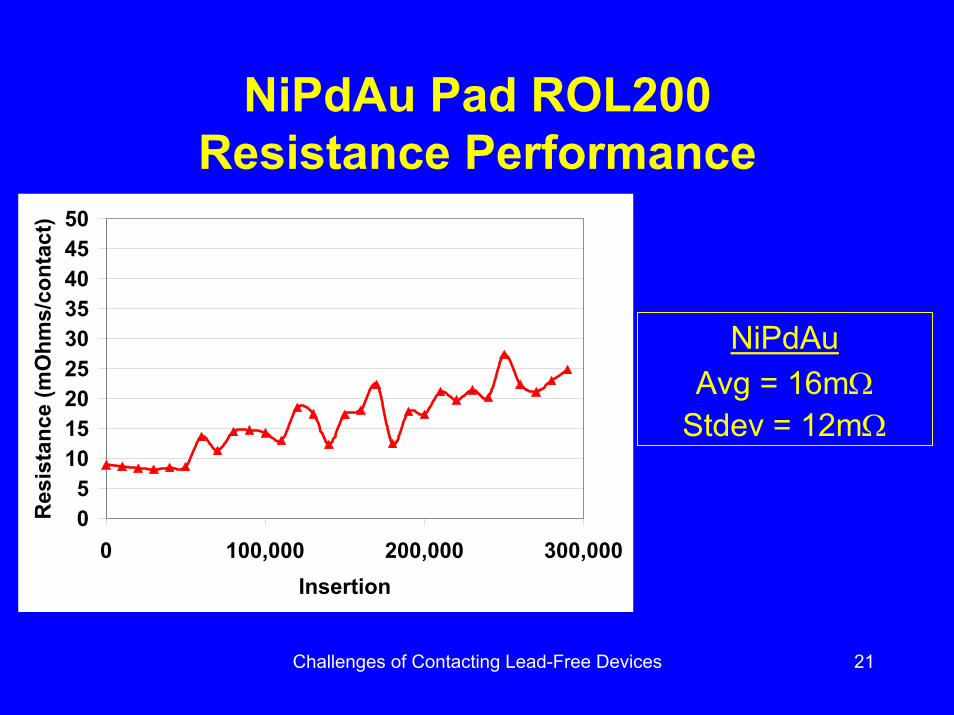
Challenges of Contacting Lead-Free Devices 21
NiPdAu Pad ROL200Resistance Performance
05
101520253035404550
0 100,000 200,000 300,000Insertion
Res
ista
nce
(mO
hms/
cont
act)
NiPdAuAvg = 16mΩ
Stdev = 12mΩ
Challenges of Contacting Lead-Free Devices 22
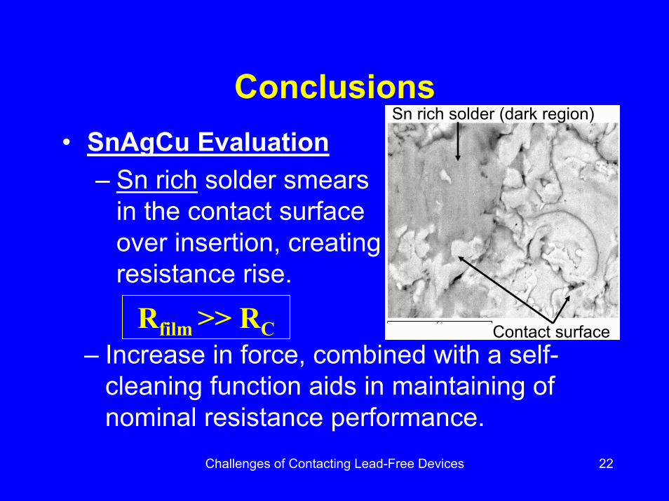
Conclusions• SnAgCu Evaluation
– Sn rich solder smears in the contact surface over insertion, creating resistance rise.
– Increase in force, combined with a self-cleaning function aids in maintaining of nominal resistance performance.
Rfilm >> RC Contact surface
Sn rich solder (dark region)

Challenges of Contacting Lead-Free Devices 23
Conclusions
• Matte Sn Evaluation– Pure Sn tend to smear
and cover the contact surface.
– A prescribed cleaning cycle aids in maintaining low resistance values, while promoting long contact life.
Rfilm >> RC

Challenges of Contacting Lead-Free Devices 24
Conclusions• NiPdAu Evaluation
– Debris/oxide presence was not detected and does not pose a problem to resistance performance. Cleaning wasn’t necessary during this test.
– Wear on un-plated contacts will reduce the force over insertion, thus increasing the variation in contact resistance.
Rc ∝ F-1/2
Challenges of Contacting Lead-Free Devices 25
Proposition for Interconnect Success
• SnAgCu and Matte Sn (Maintain Low R)– The right combination of force and self-
cleaning scrub eliminate Sn build-up on the contacts which will reduce cleaning frequency. (Reduce down time)
• NiPdAu (Promoting Long Life)– Un-plated contacts with material hardness
of >350 (Vickers) to ensure improved contact life.

Challenges of Contacting Lead-Free Devices 26
Future WorkUnderstanding Sn
• The mechanism for the increase in resistance due to the matte Sn pads and SnAgCu balls needs to be understood.
• An increase in force may reduce the need to clean as frequently, but also may reduce contact life.