challenges in achieving low cost, spectrally broad … · challenges in achieving low cost,...
TRANSCRIPT

Challenges in Achieving Low Cost, Spectrally Broad OLED
Outcoupling
Steve Forrest
Departments of Electrical Engineering and
Computer Science, and Physics
University of Michigan
Ann Arbor, MI 48109

OLEDs: Major Remaining Challenges for Lighting
• Getting the Light Out
• Blue PHOLED Lifetime
• Cost & Yield
– Patterning & Deposition
– Throughput

80% of Light is Trapped in the OLED
ηEQE = ηIQE (~100%) × ηExt ≈ 20%
Total internal reflection at the air substrate interface —substrate modes
Higher refractive indices of organic materials and ITO – waveguide modes
Organic metal interface –surface plasmon modes
3

Cathode metal (mirror)
Organics
ITO
Glass substrate
k||
k
θ
• Air modes: EQE first increases, then decreases with ETL thickness
• Waveguide modes: Only one waveguide mode TE0 due to thin ETL (<30nm). TM0 appears when >50nm.
• Surface plasmon polariton modes: Reduced with ETL thickness • Both waveguide and SPP modes are quantized • Total energy is the integral of Power Intensity cos(θ), so SPP
not as small as it looks
Where do all the photons go?
0 0.2 0.4 0.6 0.8 1 1.20
0.5
1
1.5
2
2.5
3
3.5x 10
-3
k||/k
pow
er
inte
nsity
10nm
30nm
50nm
70nm
90nm
ETL thickness
(20%) (20%)
(15%) (45%)

• Good solutions
Inexpensive
Viewing angle independent
Independent of OLED structure
• Among those things that have been tried
Optical gratings or photonic crystals1
Corrugations or grids embedded in OLED2
Nano-scale scattering centers3
Dipole orientation management
5
1Y .R. Do, et al, Adv. Mater. 15, 1214 (2003). 2Y. Sun and S.R. Forrest, Nat Phot. 2, 483 (2008). 3Chang, H.-W. et al. J. Appl. Phys. 113, - (2013).
Getting all the photons out

Substrate Modes: ~2X Improvement
ηext~40%
Microlens arrays Polymer hemispheres Much smaller than pixel
Möller, S. & Forrest, S. R. 2001. J. Appl. Phys., 91, 3324.
Several adequate solutions exist today

7
Metal electrode pixel
Organics
Low-index grid
ITO
Glass substrate
Side view
wLIG
worg
Waveguide Modes Embedded Low Index Grid
ηext~60% (incl. substrate modes)
Sun, Y. & Forrest, S. R. 2008. Nature Photon., 2, 483.
8
2mm
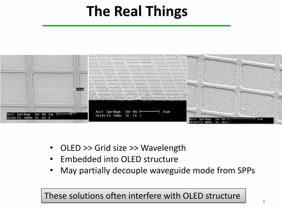
The Real Things
• OLED >> Grid size >> Wavelength • Embedded into OLED structure • May partially decouple waveguide mode from SPPs
These solutions often interfere with OLED structure

9
400 600 800
0.0
0.5
1.0
Norm
. E
L (
a.u
.)
Wavelength (nm)
Dev. 1
Dev. 4
10-6
1x10⁻⁵
1x10⁻⁴
10-3
10-2
10-1
0
10
20
30
Po
we
r E
ffic
ien
cy (
lm/W
)
Exte
rna
l Q
ua
ntu
m E
ffic
ien
cy (
%)
Current Density (mA/cm2)
Dev. 4
Dev. 3
Dev. 2
Dev. 1
0
10
20
30
40
50
60
70
80
Dev. 1 x 1.32
Dev.1x1.68
Dev. 1 x 2.3
10-3 10-2 10-1 100 101 102 10-3 10-2 10-1 100 101 102
Device Performance Using Embedded Grids + Microlens
Device 1: Conventional Device 2: LIG only Device 3: Microlenses only Device 4: LIG + Microlenses
Method is Wavelength Independent
Sun, Y. & Forrest, S. R. 2008. Nature Photon., 2, 483.

A better approach: Sub-Anode Grid
10
Cathode
nglass=1.5
nhost
norg=1.7, nITO=1.8
ngrid ngrid waveguided power + dissipation
Collect substrate mode power
Qu,Slootsky, Forrest, Nature Photonics (2015)
Multi-wavelength scale dielectric grid between glass and transparent anode (sub-anode grid)
The grid is outside of the OLED active region
Waveguided light is scattered into substrate and air modes

Emission fields
11
WITH GRID
WITHOUT GRID
VERTICAL DIPOLE
HORIZONTAL DIPOLE
Mostly in-plane (Waveguided)
Mostly out-of-plane (Glass + air)
450 500 550 600 650 700 750 8000.0
0.5
1.0
Inte
nsity (
No
rm.)
Wavelength (nm)
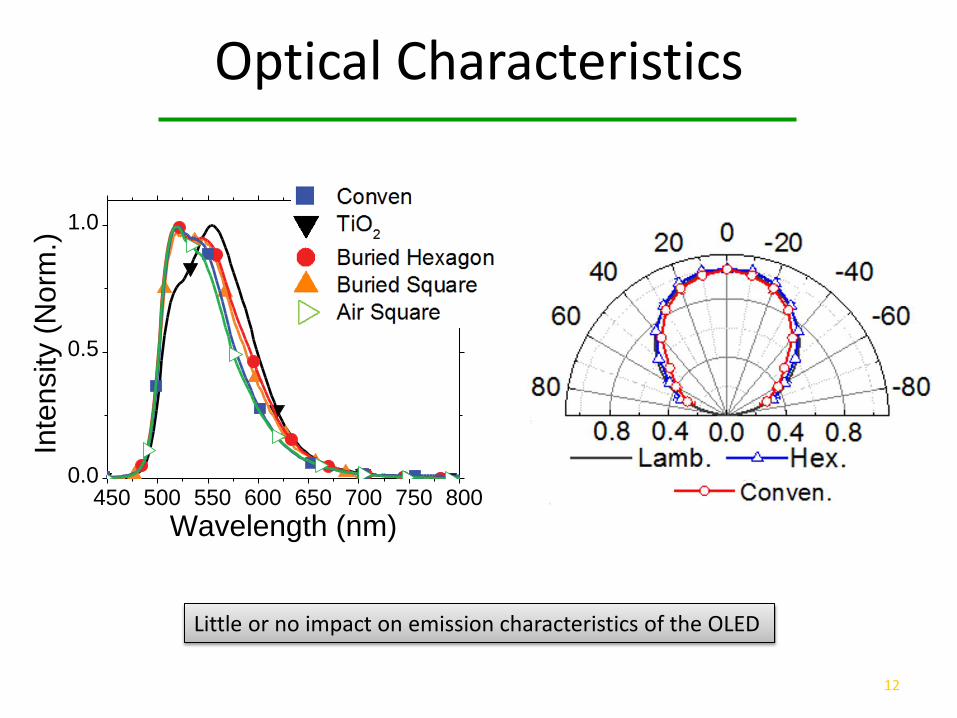
Optical Characteristics
12
Little or no impact on emission characteristics of the OLED
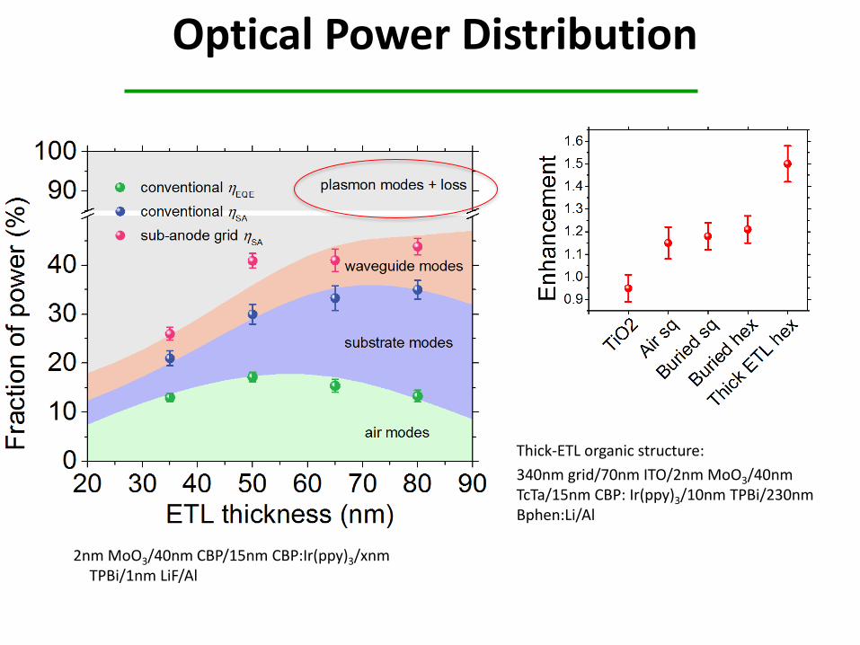
Optical Power Distribution
Thick-ETL organic structure:
340nm grid/70nm ITO/2nm MoO3/40nm TcTa/15nm CBP: Ir(ppy)3/10nm TPBi/230nm Bphen:Li/Al
2nm MoO3/40nm CBP/15nm CBP:Ir(ppy)3/xnm TPBi/1nm LiF/Al

The Last Frontier: Surface Plasmon Polariton (SPP) Modes
ηext > 80% (incl. substrate + waveguide modes)
• Waveguided light excites lossy SPPs in metal cathode • Major loss channel partially eliminated by rapid outcoupling of waveguide modes • Most difficult to eliminate cost-effectively without impacting device structure

• Simple design that does not interfere with OLED structure • Only substrate processing • Extracts all wavelengths approximately equally • 80-90% extraction within reach!
0 50 100 150
0
10
20
30
40
50
60
70
80
90
100
Power at:
460 nm
510 nm
600 nm
Air modes
Waveguide modes
Fra
cti
on
of
Po
we
r (%
)
ETL Thickness (nm)
Surface plasmon
+ Loss
SubstrateMetalmirror
ITO70nmOrganic120nm
ITO50nm
SiO2xnm
SiO2
How Much Light Can We Realistically Hope to Extract?

One possible solution: Surface corrugations
• Waveguide thickness varies due to the corrugation.
• As the thickness changes, the mode distribution changes.
• When the waveguided power travels from thin to thick areas, k|| needs to change direction to keep “being trapped”.
• Otherwise, the light is extracted.
0.8 0.85 0.9 0.95 10
0.5
1
1.5
2
2.5
3
3.5x 10
-3
k||/k
pow
er
inte
nsity
10nm
30nm
50nm
70nm
90nm
TM0
TE0
ETL thickness
Waveguide
nsub/norg=0.88
W. H. Koo, et al, Nat. Photonics 2010, 4, 222.
A possible approach: Surface buckling?
FFT
Al on resin

Substrate Au Ag Mirror on Grid Surface
SiO2 IZO Organic Anti-reflection layer
Getting Rid of SPPs Using Sub-Anode Grid + Mirror
Top Emitting OLED
3 Lift-off
Substrate Fabrication Qu
, et
al. A
CS
Ph
oto
nic
s, 2
01
7

-100 0 100 200 3000.0
0.2
0.4
0.6
0.8
1.0OrganicIZO/MoO3Dielectric
(n)
|HS
PP|2
Thickness (nm)
n=1.5,mm
n=1.8,mm
n=2.0,mm
n=2.2,mm
Metal
-100 0 100 200 3000.0
0.2
0.4
0.6
0.8
1.0
|HS
PP|2
Thickness (nm)
Ag Dielectric (n=1.5)IZO
/MoO3
a.
50 100 150 200 250 3000
20
40
60
80
100
SPPs and loss
Waveguide
modes
Po
we
r D
istr
ibu
tio
n (
%)
Dielectric thickness (nm)
air modes
Decoupling SPPs with Grid + Mirror
Thin grid regions
Thick spacer regions
Qu, et al. ACS Photonics, 2017

a. Ag
IZO/MoO3 80nm
ETL 60 nm
Substrate
EML 20 nm
HTL 40 nm
IZO/MoO3 80nm
SiO2 65 nm
Ag
IZO/MoO3 80nm
ETL 60 nm
Substrate
EML 20 nm
HTL 40 nm
IZO/MoO3 80nm
SiO2 245 nm
a. Ag
ETL 35 nm
Substrate
EML 15 nm
HTL 30 nm
Ag 15nm
Sub-electrode grid modeling
Variable Waveguide Widths Prevent Mode Propagation

0 2 4 6 8 10 12 1410
-5
10-4
10-3
10-2
10-1
100
101
102
Voltage (V)
Curr
ent D
ensity (
mA
/cm
2)
1
10
100
1000
10000
Lum
inance (
Cd/m
2)
0
20
40
60
80100
120
140
160
180
Con
Grid
0.1 1 10 1000
5
10
15
20
25
30
E
QE (
%)
Current Density (mA/cm2)
Performance with and without grid + mirror
Grid
No Grid
Qu, et al. ACS Photonics, 2017

Top emission spectra
450 500 550 600 650 7000.0
0.2
0.4
0.6
0.8
1.0
Inte
nsity
Wavelength
0o
30o
60o
450 500 550 600 650 7000.0
0.2
0.4
0.6
0.8
1.0
Inte
nsity
Wavelength (nm)
MgF2 AR Coating + Grid No AR Coating + Grid
All top emitting OLEDs show microcavity effects Effects minimized by AR coatings, diffusers, µlenses, etc.

Pt(dbq)(acac)
Isotropic Orientation
Horizontal Orientation
Manipulating Molecular Orientation
Ir(ppy)3
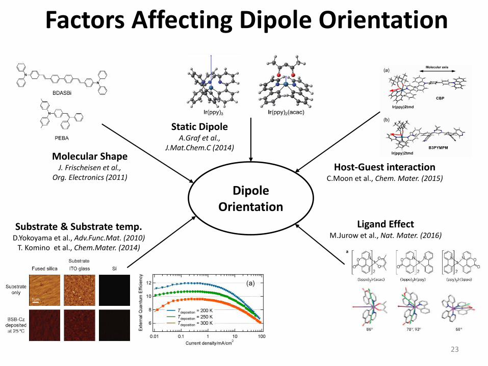
Factors Affecting Dipole Orientation
23
Dipole Orientation
Host-Guest interaction C.Moon et al., Chem. Mater. (2015)
Ligand Effect M.Jurow et al., Nat. Mater. (2016)
Molecular Shape J. Frischeisen et al.,
Org. Electronics (2011)
Substrate & Substrate temp. D.Yokoyama et al., Adv.Func.Mat. (2010)
T. Komino et al., Chem.Mater. (2014)
Static Dipole A.Graf et al.,
J.Mat.Chem.C (2014)

Use Templating to Force TDM
Orientation Thermodynamically
Driven Organization
(Amorphous)
Organization via
Molecular Anisotropy
Self-Templated Host
Pre-deposited Molecular Template
Organization via
Polycrystalline host
Dopant Molecule
(Random Alignment)
Host Molecule
(Random Alignment)
Dopant Molecule
(Anisotropic Alignment) Host Molecule
(Self-Template)
Advantage: Structure driven by growth process, not molecular design Disadvantage: Finding appropriate growth conditions to obtain structure

400 450 500 550 600 650 700 7500.0
0.5
1.0
1.5
2.0
2.5
3.0
P
L In
ten
sit
y (
No
rmalized
)
Wavelength [nm]
1vol.% PtD in PMMA
Neat PtD
Neat PtD
hor
= 0.91 0.01
Templated
hor
= 0.33 0.01
0 10 20 30 40 50 60 70 80 900.0
0.5
1.0
1.5
2.0
2.5
No
rma
lize
d I
nte
ns
ity
Detector Angle [Degree]
hor= 0.67
hor= 1.00
5 10 15 20 25 300
5x10³
1x10⁴
2[Degree]
Inte
ns
ity
[C
ou
nts
]
Neat PtD(200)
Top View
φ =
Ψ =100
Examples of Alignment via Templating
Collaborators: M. Thompson, M. Omari, J. Li

0.01 0.1 1 10 1000
2
4
6
8
10
12
EQ
E [
%]
JOLED [mA/cm2]
PtOO8:PtOEP
PtD:PtOEP
High Efficiency Devices via Self Templating
0 10 20 30 40 50 60 70 80 900.0
0.5
1.0
1.5
2.0
hor= 0.67
hor= 1.00No
rma
lize
d I
nte
ns
ity
Detector Angle [Degree]
PtD:PtOEP
hor
= 0.54 0.01
PtOO8:PtOEP
hor
= 0.73 0.01

Conclusions
• Outcoupling solutions should have these properties – Low cost
– Angle and wavelength independent
– Minimal impact on established OLED and materials designs
• Sub-anode grid outcouples all waveguide modes
• With top emission, SPP and waveguide modes not excited – No impact on electrical characteristics
– No significant optical effect
27

Thanks!
• OCM Group
– Yue Qu
– Jonchang Kim
– Michael Slootsky
• Mark Thompson
• Mohammed Omari
• Jian Li