cha4217l.pdf
TRANSCRIPT

COLOR MONITORCHA4217LCHA4227LCHA5807LCHA5227L
ManualSERVICECOLOR MONITOR CONTENTS
1. Precautions
2. Reference Information
3. Product Specifications
4. Operating Instructions
5. Disassembly & Reassembly
6. Alignment & Adjustments
7. Troubleshooting
8. Exploded View & Parts List
9. Electrical Parts List
10. Block Diagram
11. PCB Diagrams
12. Wiring Diagram
13. Schematic Diagrams

Samsung Electronics Co., Ltd. August 1998Printed in KoreaCode No.: BH68-61127A

WARNINGS1. For continued safety, do not attempt to modify the
circuit board.
2. Disconnect the AC power before servicing.
3. When the chassis is operating, semiconductorheatsinks are potential shock hazards.
1-1-1 Servicing the High Voltage VR and CRT :
WARNING:Damaged IC202 may cause excessive
x-ray emissions.
1. When servicing the high voltage system, removethe static charge by connecting a 10 kohm resistorin series with an insulated wire (such as a testprobe) between the chassis and the anode lead.
2. If the HV VR requires adjustment:This monitor does not need to adjust high voltage,high voltage step is saved at IC202, adjusting thishigh voltage to 24.5±0.5 kV - 14Ó, 25.0±0.5 kV - 15Ó.
3. When troubleshooting a monitor with excessivelyHV, avoid being unnecessarily close to the monitor.Do not operate the monitor for longer than isnecessary to locate the cause of excessive voltage.
4. High voltage should always be kept at the ratedvalue, no higher. Only when high voltage isexcessive are X-rays capable of penetrating the shellof the CRT, including the lead in glass material.Operation at high voltages may also cause failure ofthe CRT or high voltage circuitry.
5. When the HV regulator is operating properly, thereis no possibility of an X-ray problem. Make sure theHV does not exceed its specified value and that it isregulating correctly.
6. The CRT is especially designed to prohibit X-ray emissions. To ensure continued X-rayprotection, replace the CRT only with one that isthe same or equivalent type as the original.
7. Handle the CRT only when wearing shatterproofgoggles and after completely discharging the highvoltage anode.
8. Do not lift the CRT by the neck.
1-1-2 Fire and Shock Hazard :Before returning the monitor to the user, perform thefollowing safety checks:
1. Inspect each lead dress to make certain that theleads are not pinched or that hardware is notlodged between the chassis and other metal parts inthe monitor.
2. Inspect all protective devices such as nonmetalliccontrol knobs, insulating materials, cabinet backs,adjustment and compartment covers or shields,isolation resistor-capacitor networks, mechanicalinsulators, etc.
3. Leakage Current Hot Check (Figure 1-1): WARNING: Do not use an isolation transformer during
this test.Use a leakage current tester or a metering systemthat complies with American National StandardsInstitute (ANSI C101.1, Leakage Current forAppliances), and Underwriters Laboratories (ULPublication UL1410, 59.7).
4. With the unit completely reassembled, plug the ACline cord directly into a 120V AC outlet. With theunitÕs AC switch first in the ON position and thenOFF, measure the current between a known earthground (metal water pipe, conduit, etc.) and allexposed metal parts, including: metal cabinets,screwheads and control shafts. The currentmeasured should not exceed 0.5 milliamp. Reversethe power-plug prongs in the AC outlet and repeatthe test.
Figure 1-1. Leakage Current Test Circuit
1-1-4 Product Safety NoticesSome electrical and mechanical parts have specialsafety-related characteristics which are often notevident from visual inspection. The protection they givemay not be obtained by replacing them withcomponents rated for higher voltage, wattage, etc. Partsthat have special safety characteristics are identified by
on schematics and parts lists. A substitutereplacement that does not have the same safetycharacteristics as the recommended replacement partmight create shock, fire and / or other hazards. Productsafety is under review continuously and newinstructions are issued whenever appropriate.
Components identified by on schematics and partslists must be sealed by a soldering iron afterreplacement and adjustment.
CHA42*7L/5**7L 1-1
1 Precautions
1-1 Safety Precautions
!
DEVICEUNDERTEST
TEST ALLEXPOSED METAL
SURFACES
(READING SHOULDNOT BE ABOVE 0.5mA)
LEAKAGECURRENTTESTER
2-WIRE CORD
ALSO TEST WITHPLUG REVERSED
(USING AC ADAPTERPLUG AS REQUIRED) EARTH
GROUND
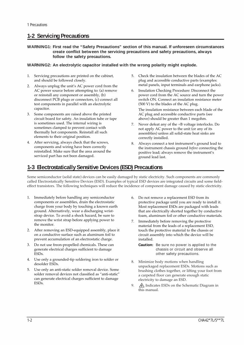
1. Servicing precautions are printed on the cabinet,and should be followed closely.
2. Always unplug the unitÕs AC power cord from theAC power source before attempting to: (a) removeor reinstall any component or assembly, (b)disconnect PCB plugs or connectors, (c) connect alltest components in parallel with an electrolyticcapacitor.
3. Some components are raised above the printedcircuit board for safety. An insulation tube or tapeis sometimes used. The internal wiring issometimes clamped to prevent contact withthermally hot components. Reinstall all suchelements to their original position.
4. After servicing, always check that the screws,components and wiring have been correctlyreinstalled. Make sure that the area around theserviced part has not been damaged.
1. Immediately before handling any semiconductorcomponents or assemblies, drain the electrostaticcharge from your body by touching a known earthground. Alternatively, wear a discharging wrist-strap device. To avoid a shock hazard, be sure toremove the wrist strap before applying power tothe monitor.
2. After removing an ESD-equipped assembly, place iton a conductive surface such as aluminum foil toprevent accumulation of an electrostatic charge.
3. Do not use freon-propelled chemicals. These cangenerate electrical charges sufficient to damageESDs.
4. Use only a grounded-tip soldering iron to solder ordesolder ESDs.
5. Use only an anti-static solder removal device. Somesolder removal devices not classified as Òanti-staticÓcan generate electrical charges sufficient to damageESDs.
5. Check the insulation between the blades of the ACplug and accessible conductive parts (examples:metal panels, input terminals and earphone jacks).
6. Insulation Checking Procedure: Disconnect thepower cord from the AC source and turn the powerswitch ON. Connect an insulation resistance meter(500 V) to the blades of the AC plug.
The insulation resistance between each blade of theAC plug and accessible conductive parts (seeabove) should be greater than 1 megohm.
7. Never defeat any of the +B voltage interlocks. Donot apply AC power to the unit (or any of itsassemblies) unless all solid-state heat sinks arecorrectly installed.
8. Always connect a test instrumentÕs ground lead tothe instrument chassis ground before connecting thepositive lead; always remove the instrumentÕsground lead last.
6. Do not remove a replacement ESD from itsprotective package until you are ready to install it.Most replacement ESDs are packaged with leadsthat are electrically shorted together by conductivefoam, aluminum foil or other conductive materials.
7. Immediately before removing the protectivematerial from the leads of a replacement ESD,touch the protective material to the chassis orcircuit assembly into which the device will beinstalled.
Caution: Be sure no power is applied to the chassis or circuit and observe all other safety precautions.
8. Minimize body motions when handlingunpackaged replacement ESDs. Motions such asbrushing clothes together, or lifting your foot froma carpeted floor can generate enough staticelectricity to damage an ESD.
9. Indicates ESDs on the Schematic Diagram inthis manual.
1 Precautions
1-2 CHA42*7L/5**7L
1-3 Electrostatically Sensitive Devices (ESD) Precautions
Some semiconductor (solid state) devices can be easily damaged by static electricity. Such components are commonlycalled Electrostatically Sensitive Devices (ESD). Examples of typical ESD devices are integrated circuits and some field-effect transistors. The following techniques will reduce the incidence of component damage caused by static electricity.
1-2 Servicing Precautions
WARNING1: First read the “Safety Precautions” section of this manual. If unforeseen circumstances
create conflict between the servicing precautions and safety precautions, always
follow the safety precautions.
WARNING2: An electrolytic capacitor installed with the wrong polarity might explode.

CHA42*7L/5**7L 2-1
2 Reference Information
2-1 List of Abbreviations, Symbols and Acronyms
2-1-1 Abbreviations
Abbreviation Definition Abbreviation Definition
ASS’Y AssemblyB BlueB+ ADJ B+ AdjustmentB-CUT Blue-CutoffB-GAIN Blue GainBRIGHT BrightnessC R-CompositionC-MIC Condenser MicrophoneCLK ClockCM R-CementCN ConnectorCONT ContrastD-SUB D-SubminiatureEEP-CLK Electrically Erasable and
Programmable ClockEXT ExternalEXT-MIC External MicrophoneFreq. FrequencyFU FusibleG GreenG-CUT Green-CutoffG-GAIN Green GainGND GroundH HorizontalH HeaterH-DRV Horizontal DriveH-DY Horizontal Deflection YorkH-FLB Horizontal FlybackH-FV Horizontal-Feedback VoltageH-LIN Horizontal LinearityH-POSI Horizontal PositionH-SIZE Horizontal SizeH/PHONE HeadphoneHz HertzI-SENSE Current-Senselb PoundMAX MaximumMIC MicrophoneMIN MinimumMP C-Metalized PolyesterMPP Metal PolypropyleneMO R-Metal Oxide
OSC OscillatorP C-PolyesterPARA ParabolaPARALL ParallelogramPIN-BAL Pincushion BalancePRE-AMP Pre-AmplifierPS1 Power Saving1 (suspend)PS2 Power Saving2 (off)PWR PowerR RedR-CUT Red-CutoffR-GAIN Red GainRST ResetS-PIN Side PincushionS-RASTER Self RasterS/W SwitchSCAP S Correction CapacitorSPK SpeakerSYNC SynchronizationT C-TantalumTR TransistorTRAP TrapezoidU-COM MicroprocessorV VerticalV-DY Vertical Deflection YorkV-FLB Vertical FlybackV-LIN Vertical LinearityV-MUTE Video MuteV-OUT Vertical OutputV-PARA Vertical ParabolaV-POL V-PolarityV-POSI Vertical PositionV-SENSE Voltage-SenseV-SIZE Vertical SizeWW R-Wire WoundX-TAL CrystalΩ ohmKΩ 1000 ohmMΩ 1000 KΩuF microfarad (10-6F)nF nanofarad (10-9F)pF picofarad (10-12F)

2 Reference Information
2-2 CHA42*7L/5**7L
Acronym Definition Acronym Definition
ABL Automatic Brightness Limits
AC Alternating Current
ACL Automatic Contrast Limit
AFC Automatic Frequency Control
ANSI American National Standards Institute
CMOS Complementary Metal Oxide Semiconductor
CRT Cathode Ray Tube
DC Direct Current
DDC Data Display Channel
DF Dynamic Focus
DMM Digital Multimeter
DPMS Display Power Management Signaling
DVM Digital Voltmeter
DY Deflection York
EEPROM Electrically Erasable andProgrammable Read only Memory
ESD Electrostatically Sensitive Device
ESF Electronic Static Field
FBT Flyback Transformer
FET Field Effect Transistor
FH Horizontal Frequency
FS Fail Safe
FV Vertical Frequency
GD Geometric Distortion
H/V Horizontal/Vertical
HV High Voltage
I/O Input/Output
IC Integrated Circuit
LED Light Emitting Diode
MAC Macintosh
MOFA Mask Outside Frame Assemble
OCP Over Current Protection
OP AMP Operational Amplifier
OSD On Screen Display
P-P Peak to Peak
PCB Printed Circuit Board
PLL Phase Locked Loop
PWM Pulse Width Modulation
SMPS Switch Mode Power Supply
SVGA Super Video Graphics Array
SWEDAC
TP Test Point
UL Underwriters Laboratories
USB Universal Serial Bus
VESA Video Electronics Standard Association
VGA Video Graphics Array
VR Variable Registor
W/B White Balance
2-1-2 Acronyms
2-1-2 Symbols
Can emit X-radiation
Hot Ground
Cold Ground
Electrostatically Sensitive Device (ESD)
Provides special safety considerations!

CHA42*7L/5**7L 3-1
3 Product Specifications
3-1 Specifications
Picture Tube: CHA42*7L: 14-Inch (36 cm); 13.2-Inch (33.5 cm) viewable, 90° Deflection,CHA5**7L: 15-Inch (38 cm); 13.8-Inch (35 cm) viewable, flat-face tube, 90° Deflection, 0.28 mm Dot pitch, Semi-tint, Non-glare, Antistatic silica coating, Invar shadow mask
Scanning Frequency Horizontal: 30 kHz to 55 kHz (Automatic) - 14” / 30 kHz to 61 kHz (Automatic) - 15”Vertical: 50 Hz to 125 Hz (Automatic)
Display Colors Unlimited colors
Maximum Resolution Horizontal : 1024 Dots Vertical : 768 Lines
Input Video Signal Analog, 0.714 Vp-p positive at 75 Ω, internally terminated
Input Sync Signal Separate Sync : TTL level positive/negative
Maximum Pixel Clock 14” : 65 MHz, 15” : 85 MHz
Active Display 14” 15”
Horizontal 255 mm ± 3 mm (4:3 ratio) 267 mm ± 3 mm (4:3 ratio) Vertical 191 mm ± 3 mm 200 mm ± 3 mm
Input Voltage AC 90 to 264 Volts, 60 Hz/50 Hz ± 3 Hz
Power Consumption 73 Watt
Dimensions 14” 15”
Unit (W x D x H) 13.7 x 15.2 x 14.3 Inches (348 x 385 x 362.5 mm) 14.6 x 15.6 x 14.8 Inches (370 x 395 x 377 mm)Carton (W x D x H) 16.6 x 18.1 x 15.4 Inches (422 x 460 x 390 mm) 17.9 x 19.6 x 17.0 Inches (454 x 497 x 433 mm)
Weight (Net/Gross) CHA42*7L : 23.1 lbs (10.5 kg) / 27.3 lbs (12.4 kg)CHA5**7L : 27.6 lbs (12.5 kg) / 30.9 lbs (14.0 kg)
Environmental Considerations Operating Temperature : 32°F to 104°F (0°C to 40°C)Humidity : 10 % to 80 %
Storage Temperature : -4°F to 113°F (-20°C to 45°C)Humidity : 5 % to 95 %
CRT Code No.
• CHA42*7L/5**7L complies with SWEDAC (MPR II) recommendations for reduced electromagnetic fields.• Designs and specifications are subject to change without prior notice.
Item Description

3 Product Specifications
3-2 CHA42*7L/5**7L
3-2 Pin Assignments
SyncType
Pin No.
15-Pin Signal Cable Connector (Figure 3-1)
Separate
1
2
3
4
5
6
7
8
9
10
11
12
13
14
15
Red
Green
Blue
GND
DDC Return
GND-R
GND-G
GND-B
Reserved
GND-Sync/Self-raster
GND
DDC Data
H-Sync
V-Sync
DDC Clock
5
15
Figure 3-1. Male Type

3 Product Specifications
CHA42*7L/5**7L 3-3
fH (kHz)
A µsec
B µsec
C µsec
D µsec
E µsec
fV (Hz)
O msec
P msec
Q msec
R msec
S msec
ClockFrequency(MHz)
PolarityH.Sync
V.Sync
Remark
IBM VESA
800/85 Hz800 x 600
1024/60 Hz1024 x 768
(14”)
1024/75 Hz1024 x 768
(15”)
640/60 Hz640 x 480
720/70 Hz720 x 400
31.469
31.777
3.813
1.907
25.422
0.636
70.087
14.268
0.064
1.080
12.711
0.413
28.322
Negative
Positive
Separate
31.469
31.778
3.813
1.907
25.422
0.636
59.940
16.683
0.064
1.048
15.253
0.318
25.175
Negative
Negative
Separate
37.500
26.667
2.032
3.810
20.317
0.508
75.000
13.333
0.080
0.427
12.800
0.027
31.500
Negative
Negative
Separate
43.269
23.111
1.556
2.222
17.778
1.556
85.008
11.764
0.069
0.578
11.093
0.023
36.000
Negative
Negative
Separate
46.875
21.333
1.616
3.232
16.162
0.323
75.000
13.333
0.064
0.448
12.800
0.021
49.500
Positive
Positive
Separate
53.674
18.631
1.138
2.702
14.222
0.569
85.061
11.756
0.056
0.503
11.179
0.019
56.250
Positive
Positive
Separate
48.363
20.677
2.092
2.462
15.754
0.369
60.004
16.666
0.124
0.600
15.880
0.062
65.000
Negative
Negative
Separate
60.023
16.660
13.003
3.658
13.206
3.454
75.029
13.328
12.795
0.533
12.812
0.516
78.750
Positive
Positive
Separate
800/75 Hz800 x 600
640/75 Hz640 x 480
640/85 Hz640 x 480
3-3 Timing Chart
This section of the service manual describes the timing that the computer industry recognizes as standardfor computer-generated video signals.
Q R S
P
O
Video
Sync Sync
Horizontal Vertical
C D E
P
O
B
A
Video
Sync Sync
Separate Sync
Table 3-1. Timing Chart
Mode
Timing
C D
A O
E
B P
Video
Sync Sync
Video
Q R S
A : Line time total B : Horizontal sync width O : Frame time total P : Vertical sync width
C : Back porch D : Active time Q : Back porch R : Active time
E : Front porch S : Front porch
VIDEOA
B OP
Q R S
Horizontal Vertical
H/V Composite Sync

Memo
3 Product Specifications
3-4 CHA42*7L/5**7L

CHA42*7L/5**7L 4-1
Location Symbol Description
1 Power Button
Power Indicator LED
Adjustment Buttons
Side Pincushion Button
Horizontal Position Button
Trapezoid Button
Brightness Control
Contrast Control
Parallelogram
V-Linearity
Pinbalance Button
Degauss
Recall
User Delete
Tilt (Option: 15”)
V-Moire
Vertical Size Button
Vertical Position Button
Horizontal Size Button
3
4
8
9
10
11
12
13
14
15
16
17
18
19
5
6
7
2
3
1213
14 1716
15
4 5
18
6 7 8 9 10 11
12
19
Table 4-1. Front Panel Controls
Figure 4-1. Front Control Panel
+
+
+
+
+
+
+
+
4 Operating Instructions
4-1 Front View and Control
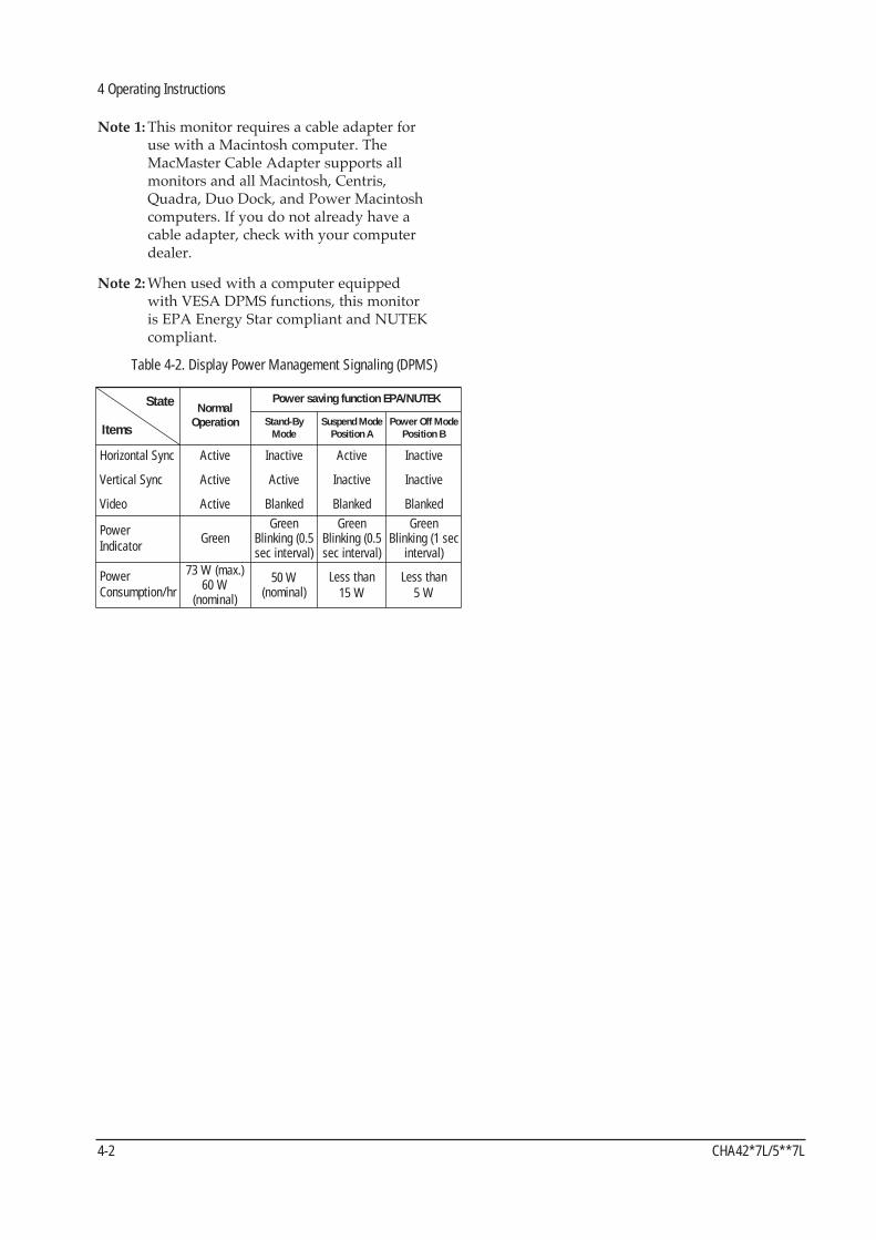
Note 1: This monitor requires a cable adapter foruse with a Macintosh computer. TheMacMaster Cable Adapter supports allmonitors and all Macintosh, Centris,Quadra, Duo Dock, and Power Macintoshcomputers. If you do not already have acable adapter, check with your computerdealer.
Note 2: When used with a computer equippedwith VESA DPMS functions, this monitoris EPA Energy Star compliant and NUTEKcompliant.
4 Operating Instructions
4-2 CHA42*7L/5**7L
State
Items
NormalOperation
Horizontal Sync
Vertical Sync
Video
PowerIndicator
PowerConsumption/hr
Active
Active
Active
GreenGreen
Blinking (0.5sec interval)
GreenBlinking (0.5sec interval)
GreenBlinking (1 sec
interval)73 W (max.)
60 W(nominal)
Less than15 W
50 W (nominal)
Less than5 W
Inactive
Active
Blanked
Active
Inactive
Blanked
Power saving function EPA/NUTEK
Stand-ByMode
Suspend ModePosition A
Power Off ModePosition B
Inactive
Inactive
Blanked
Table 4-2. Display Power Management Signaling (DPMS)

5-1-1 Cabinet Disassembly
1. With a pad beneath it, stand the monitor on itsfront with the screen facing downward andthe base closest to you. Make sure nothing willdamage the screen.
2. Working from the back of the monitor, removethe four screws and remove the Rear Cover.
3. Using pinch-nose pliers or long-nose pliers,carefully disconnect the Anode Cap from theCRT.
Caution: Do not touch the anode contact onthe CRT.
5-1-2 Removing the CRT Socket PCB
1. Complete all previous steps.2. Disconnect CRT and Main PCB ground wires
on CRT Socket PCB and Shield Cover.3. Desolder the 5 tabs on the underside of the
CRT Socket PCB shield and remove the CRTSocket PCB Shield.
4. Using a knife, cut through the silicone bondand lift off the CRT Socket PCB.
5. Disconnect connectors CN102 and CN103 onthe CRT Socket PCB.
6. Using a solder iron, disconnect CN202_2.7. Disconnect CRT Socket and Focus (G3) wires
on CRT Socket PCB.8. Place Video PCB on a flat, level surface that is
protected from static electricity.
5-1-3 Removing the Main PCB
1. Complete all previous steps.2. Disconnect Degaussing Coil at the CN601
connector on the Main PCB.3. Disconnect all easily accessible ground wires
on the Main PCB and Chassis Bottom.4. Disconnect the DY connector between the DY
and the CN301, CN302, CN502 and CN503connector on the Main PCB.
5. Remove the screws on the back and alongeach side of the Chassis Bottom.
6. Carefully lift the Main PCB AssÕy.7. Remove all other ground wires.
5-1-4 CRT Ass’y Disassembly
1. Complete all previous steps.2. Straighten the Degaussing Coil Assembly
coated metal ties and lift Coil AssÕy from theCRT.
3. Remove the four corner screws and lift theCRT up and away from the Front CoverAssembly and place it on a padded surface.
Caution: Do not lift the CRT by the neck.If you will be returning this CRT tothe monitor, be sure to place the CRTface downward on a protective pad.
CHA42*7L/5**7L 5-1
5 Disassembly and ReassemblyThis section of the service manual describes the disassembly and reassembly procedures for theCHA42*7L/5**7L monitors.
WARNING: This monitor contains electrostatically sensitive devices. Use caution when handling
these components.
5-1 Disassembly
Cautions:1. Disconnect the monitor from the power source before disassembly.2. Follow these directions carefully; never use metal instruments to pry apart the cabinet.

5 Disassembly and Reassembly
5-2 CHA42*7L/5**7L
Memo

6-1-1 Before Making Adjustments
6-1-1 (a) ORIENTATIONWhen servicing, always face the monitor to theeast.
6-1-1 (b) MAGNETIC FIELDSWhenever possible, use magnetic field isolationequipment such as a Helmholtz field to surroundthe monitor. If a Helmholtz field is not available,frequently degauss the unit under test.
Caution: Other electrical equipment may causeexternal magnetic fields which mayinterfere with monitor performance.
Use an external degaussing coil to limit magneticbuild up on the monitor. If an external degaussingcoil is not available, use the internal degaussingcircuit. However, do not use the internaldegaussing circuit more than once per 30 minutes.
6-1-1 (c) WARM-UP TIMEThe monitor must be on for 30 minutes beforestarting alignment procedures. Warm-up time isespecially critical in Color Temperature and WhiteBalance adjustments.
6-1-1 (d) SIGNALAnalog, 0.714 Vp-p positive at 75 ohm, internalterminationSync: Separate (TTL level negative/positive)
6-1-1 (e) SCANNING FREQUENCYHorizontal: 30 kHz to 55 kHz (automatic)-14Ó
30 kHz to 61 kHz (automatic)-15ÓVertical: 50 Hz to 120 Hz (automatic)Unless otherwise specified, adjust at the 800 x 600mode (H : 53.7 kHz, V: 85 Hz)-15Ó, the 640 x 480mode (H : 43.8 kHz, V: 85 Hz)-14Ó signals. Refer to Table on page 3-3.
6-1-1 (f) +B 13 V LINE CHECKNo beam Contrast: Maximum Brightness: Maximum Check the DC 13 V ± 0.2 V at Cathode of D616Point and GND.
6-1-1 (g) HIGH VOLTAGE CHECKNo beamContrast: Maximum Brightness: MaximumCheck the high voltage to 24.5 ± 0.5 kV - 14Ó, 25 ± 0.5 kV - 15Ó at anode and GND.
6-1-1 (i) CENTER RASTERAdjust VR502 so that the back raster comes to thecenter when you apply a signal of 53.7 kHz/85 Hz - 14Ó, 60 kHz/75 Hz - 15Ó .
6-1-1 (j) BRIGHTNESS AND CONTRASTUnless otherwise specified, adjust brightness andcontrast buttons:Brightness: Maximum
(press ⊕ button until the LED is blink)Contrast: Maximum
(press ⊕ button until the LED is blink)
CHA42*7L/5**7L 6-1
6 Alignment and AdjustmentsThis section of the service manual explains how to make permanent adjustments to the monitor. Directionsare given for adjustments using the monitor Interface Board Ver. 2.0 and software (SoftJig).
6-1 Adjustment Conditions
Caution: Changes made without the SoftJig are saved only to the user mode settings. As such, thesettings are not permanently stored and may be inadvertently deleted by the user.

6-1-2 Required Equipment
The following equipment may be necessary foradjustment procedures:
6-1-2 (a) DISPLAY CONTROL ADJUSTMENT1. Non-metallic (Ð) screwdriver: 1.5 mm
Non-metallic (Ð) screwdriver: 3 mm2. Philips (+) screwdriver: 1.5 mm3. Non-metallic hexkey: 2.5 mm4. Digital Multimeter (DMM), or
Digital Voltmeter (DVM)5. Signal generator, or
Computer with a video board that uses theET-4000 chipset (strongly recommended ifusing Samsung DM 200 software) and thatdisplays: 800 x 600 @ 85 Hz, or 800 x 600 @ 75 Hz (minimum).
6. Personal computer7. Required software: Softjig.exe from Samsung,
Samsung DM200, or DisplayMate forWindows from Sonera Technologies
8. Interface Board Ver. 2.0 Code No. BH81-90001K
9. Parallel communications cable (25-pin to 25-pin); Code No. BH81-90001H
10. Signal cable (15-pin to 15-pin cable withadditional 3-pin connector); Code No. BH81-90001J
11. 5 V DC adapter, not supplied
Note: SoftJig Assembly (includes items 8, 9 and 10Code No. BH81-90001L
6-1-2 (b) COLOR ADJUSTMENTS1. All equipment listed in 6-1-2 (a), above2. Color analyzer, or any luminance
measurement equipment
6-1-3 Connecting the SoftJigConnect the monitor to the signal generator and/or PC as illustrated in Figures 6-1 and 6-2.Note: The signal cable connector which includes
the 3-wire cable must connect to themonitor. If you use Setup 2 (PC only, nosignal generator) you can only makeadjustments to the signal timing availableon that computer system. To makecorrections to all factory timings requiresthe use of an additional signal generator.
6-1-4 After Making Adjustments
After finishing all adjustments, test the monitor inall directions. If, for example, the monitor does notmeet adjustment specifications when facing north,reposition the monitor to face east and readjust.This time, try for an adjustment closer to the idealsetting within the tolerance range. Test the unitagain in all directions. If the monitor again fails tomeet specifications in every direction, contactyour Regional After Service Center for possibleCRT replacement.
6 Alignment and Adjustments
6-2 CHA42*7L/5**7L
MONITOR
INTERFACEBOARD VER. 2.0
PCSIGNALGENERATOR
7 PIN MINI DINCONNECTOR
SIGNAL CABLE
5V DCADAPTOR
PARALLEL CABLE
Figure 6-1. Setup 1, With Signal Generator
MONITOR
INTERFACEBOARD VER. 2.0
PC
7 PIN MINI DINCONNECTOR
SIGNAL CABLEPARALLEL CABLE
D-SUBCONNECTOR
5V DCADAPTOR
Figure 6-2. Setup 2, Without Signal Generator

6-2-1 Centering
Centering means to position the center point ofthe display in the middle of the display area.Horizontal size and position and vertical size andposition control the centering of the display.
Adjust the horizontal size and vertical size to theiroptimal settings: 267 mm (H) x 200 mm (V) for15Ó, 255 mm (H) x 191 mm (V) for 14Ó
Adjust the horizontal position and verticalposition to within 4.0 mm of the center point ofthe screen.
l A - B l ² 5.0 mm.l C - D l ² 5.0 mm.
6-2-1 (a) HORIZONTAL MINIMUM SIZE ADJUSTMENT
CONDITIONSScanning frequency: 53.7 kHz/85 Hz (15Ó)
43.3 kHz/85 Hz (14Ó)Display image: Crosshatch patternBrightness: MaximumContrast: Maximum
PROCEDUREHorizontal minimum size can be adjusted asfollows using Softjig.1. Display the timing 800 x 600/85 Hz (15Ó),
640 x 480/85 Hz (14Ó).2. Adjust horizontal size to minimum size using
H_SIZE.3. Adjust horizontal minimum size to 250 mm
(15Ó) or 242 mm (14Ó) using H_SIZE MIN.4. Adjust horizontal size to 267 mm (15Ó) or
255 mm (14Ó) using H_SIZE.5. Press the ALL MODE SAVE horizontal
minimum size for each timing is savedautomatically.
If horizontal minimum size range cannot meet thespec, horiontal maximum size of 640 x 480/75 Hzincluding 800 x 600/60 Hz, 56 Hz, may besaturated or cannot overscan the bezel.
6-2-1 (b) VERTICAL SIZE ADJUSTMENT
CONDITIONSScanning frequency: 53.7 kHz/85 Hz (15Ó)
43.3 kHz/85 Hz (14Ó)Display image: Crosshatch patternBrightness: MaximumContrast: Maximum
Adjust the vertical size of the display pattern to200 mm (15Ó) and 191 mm (14Ó). (Tolerance: ± 3 mm.)
6-2-1 (c) HORIZONTAL POSITION ADJUSTMENT
CONDITIONSScanning frequency: 53.7 kHz/85 Hz (15Ó)
43.3 kHz/85 Hz (14Ó)Display image: Crosshatch pattern
PROCEDURECenter the test pattern on the raster.
6-2-1 (d) VERTICAL POSITION ADJUSTMENT
CONDITIONSScanning frequency: 53.7 kHz/85 Hz (15Ó)
43.3 kHz/85 Hz (14Ó)Display image: Crosshatch pattern
Center the test pattern on the raster.
6-2-2 LinearityLinearity affects the symmetry of images as theyappear on the screen. Unless each row or columnof blocks in a crosshatch pattern is of equal size,or within the tolerances shown in Tables 6-1 and6-2, an image appears distorted, elongated orsquashed.
The formular of linearity (%)
Table 6-1. Standard Modes Linearity: 800 x 600/85Hz - 15”640 x 480/85 Hz - 14”
Table 6-2. Other Modes Linearity: VGA, SVGA, XGA, MAC, etc.
6 Alignment and Adjustments
CHA42*7L/5**7L 6-3
6-2 Display Control Adjustments
C
A
DISPLAY AREA
EDGE OF BEZELB
D
Figure 6-3. Centering
Supported Timing Mode
Each block (14 %) Difference betweenadjacent blocks (5 %)
Standard Timing Modes
Each block (10 %) Difference betweenadjacent blocks (4 %)
2 x (Max – Min)= x 100
Max + Min

6-2-3 Trapezoid Adjustment
CONDITIONSScanning frequency: 53.7 kHz/85 Hz (15Ó)
43.3 kHz/85 Hz (14Ó)Display image: Crosshatch patternMake the the test pattern rectangular.
Figure 6-4. Trapezoid
6-2-4 Parallelogram Adjustment
CONDITIONSScanning frequency: 53.7 kHz/85 Hz (15Ó)
43.3 kHz/85 Hz (14Ó)Display image: Crosshatch patternTo activate the Parallelogram Adjustmentfunction, push both the Horizontal Position andVertical Position buttons and hold them in forlonger than 3 seconds, or until the power indicatorLED changes from green to blink and back togreen. Use the Increase (+) and Decrease (Ð) buttons tocorrect the display shape.
Figure 6-5. Parallelogram
6-2-5 Side Pincushion Adjustment
CONDITIONSScanning frequency: 53.7 kHz/85 Hz (15Ó)
43.3 kHz/85 Hz (14Ó)Display image: Crosshatch patternAfter pushing the Side Pincushion button once,push the Increase (+) and Decrease (Ð) buttons tostraighten the sides of the test pattern.
6-2-6 CRT Tilt Adjustment
TILT ADJUSTMENT (CHA5807L With Tilt)Push the V-Posi and H-Size simultaneously untilLed blinks and back on again. Push the Increase(+) and Decrease (Ð) buttons to correct the Tilt.
6-2-7 Vertical Linearity Adjustment
To activate the vertical linearity adjustment, pushboth the horizontal position and horizontal sizebuttons and hold then in for longer than 3seconds, or until the power indicator LED changesfrom green to blink and back to green. Use the Increase (+) and Decrease (Ð) buttons tocorrect the display shape.
6-2-8 Pin Balance Adjustments
To activate the pin balacne function, push both thehorizontal position and vertical Size buttons andhold then in for longer than 3 seconds, or until thepower indicator LED changes from green to blinkand back to green. Use the Increase (+) and Decrease (Ð) buttons tocorrect the display shape.
6-2-9 Degauss
Push the contrast and brightness buttonssimultaneously. The degaussing circuit caneffectively function only once per 30 minutes. Ifavailable, use an external degaussing coil duringservicing.
6-2-10 Delete User Mode Data
To delete the picture data from the user modes,push the contrast button and side pincushionbutton for 5 or more seconds simultaneously.
6-2-11 Recall
To delete the picture data from current user mode,push the contrast button and trapzoid button for 5or more seconds simultaneoulsy.
6 Alignment and Adjustments
6-4 CHA42*7L/5**7L
2.2 mm 2.2 mm
| C1 |, | C2 | ≤ 2.0 mm, | D1 |, | D2 | ≤ 2.2 mm.
Figure 6-6. Pincushion
A B
C
D
FRONT BEZEL
BACK RASTER
Figure 6-7. CRT Tilt Adjustment
2.2 mm 2.2 mm
C2
D2D1
C1
2.2 mm

Note 1: Color adjustment of this mode is controledby Micom Jig or software.
Note 2: To make color adjustments you must havea color analyzer and one of the followingconfigurations:
1. Signal Generatoror
2. Computer with Samsung DM 200 software orDisplayMate for Windows software fromSonera Technologies
3. In case of CHA5**7L, use 800 x 600 modesignal (53.7 kHz/85 Hz) for adjustments, incase of CHA42*7L, use 640 x 480 mode signal(43.3 kHz/85 Hz).
Before making adjustments, check that the videosignals are as follows:
Video : Analog, 0.714 Vp-p (at 75 ½ termination)Sync : Separate TTL level
Unless otherwise specified, use 800 x 600 mode signal (53.7 kHz/85 Hz) for adjustments.
6-3-1 Color Coordinates (Temperature)
Color temperature is a measurement of theradiant energy transmitted by a color. Forcomputer monitors, the color temperature refersto the radiant energy transmitted by white. Colorcoordinates are the X and Y coordinates on thechromaticity diagram of wavelengths for thevisible spectrum.
CONDITIONSMeasurement instrument: Color analyzerScanning frequency: 53.7 kHz/85 Hz (15Ó)
43.3 kHz/85 Hz (14Ó)Display image: White flat field at
center of display areaLuminance: Maximum
PROCEDUREUsing the directions in sections 6-3-2 through 6-3-5, adjust the Color Coordinates for 9300K to x = 0.283 ± 0.02 and y = 0.298 ± 0.02
6-3-2 Back Raster Color Adjustment
CONDITIONSMeasurement instrument: Color analyzerScanning frequency: 53.7 kHz/85 Hz (15Ó)
43.3 kHz/85 Hz (14Ó)Display image: Back raster patternBrightness: MaximumContrast: Maximum
PROCEDURE1. Adjust the Screen VR on the FBT so that the
brightness of the Back Raster is 0.3 to 0.5 ft-L(typically 0.4 ft-L).
2. Adjust the G_CUT to center.3. Adjust the B_CUT to set the ÒyÓ coordinate to
0.298 ± 0.02.4. Adjust the R_CUT to set the ÒxÓ coordinate to
0.283 ± 0.02.
Note: If the above adjustments cannot be done toeach coordinate, adjust G_CUT to increaseor decrease the green cutoff and repeatprocedures 3 and 4.
6-3-3 Video Gain Adjustment
Figure 6-8. Green Box Pattern
CONDITIONSMeasurement instrument: Color analyzerScanning frequency: 53.7 kHz/85 Hz (15Ó)
43.3 kHz/85 Hz (14Ó)Display image: Green box pattern
within range for which the ABL circuit is not active (1/3 to 1/2H and1/3 to 1/2V).
Brightness: MaximumContrast: Maximum
PROCEDURE1. Adjust G-Gain so that the brightness of the
green gain is 40 ± 1 ft-L (typically 40 ft-L).
6-3-4 White Balance Adjustment
Figure 6-9. Full White Pattern
6 Alignment and Adjustments
CHA42*7L/5**7L 6-5
6-3 Color Adjustments
1/3H-1/2H
1/3V-1/2V
FRONT BEZEL OPENING
BACK RASTER
GREEN WINDOW
FRONT BEZEL OPENING
BACK RASTER
WHITE WINDOW

CONDITIONSMeasurement instrument: Color analyzerScanning frequency: 53.7 kHz/85 Hz (15Ó)
43.3 kHz/85 Hz (14Ó)Display image: Full white patternBrightness: MaximumContrast: Maximum
PROCEDURE1. Display the full white pattern.2. Adjust R-Gain and B-Gain so that the video is
white. (x = 0.283 ± 0.02 and y = 0.298 ± 0.02)
6-3-5 White Balance Fine Adjustment
CONDITIONSMeasurement instrument: Color analyzerScanning frequency: 53.7 kHz/85 Hz (15Ó)
43.3 kHz/85 Hz (14Ó)Display image: Full white patternX-Y coordinates: x = 0.283 ± 0.02
y = 0.298 ± 0.02
PROCEDURE1. Adjust the Contrast control so that the
brightness of the video is about 5 ft-L.2. Check whether the white coordinates of the
video meet the specification above. If they donot, adjust them so that they do.
3. Adjust the Contrast to maximum luminance.4. Check whether the white coordinates still
meet the specification above. If they do not,adjust them so that they do.
6-3-6 ABL Point Adjustment
CONDITIONSMeasurement instrument: Color analyzerScanning frequency: 53.7 kHz/85 Hz (15Ó)
43.3 kHz/85 Hz (14Ó)Display image: Full white patternBrightness: MaximumContrast: Maximum
PROCEDUREAdjust ABL so that the brightness level is 35 ± 1 ft-L.
6-3-7 Focus Adjustment
CONDITIONSMeasurement instrument: Color analyzerScanning frequency: 53.7 kHz/85 Hz (15Ó)
43.3 kHz/85 Hz (14Ó)Display image: ÒHÓ character patternBrightness: MaximumContrast: Maximum
PROCEDURE1. Adjust the Focus VR on the FBT to display the
sharpest image possible.2. Use Locktite to seal the Focus VR in position.
6-3-8 Luminance Uniformity Check
CONDITIONSMeasurement instrument: Color analyzerScanning frequency: 53.7 kHz/85 Hz (15Ó)
43.3 kHz/85 Hz (14Ó)Display image: White flat fieldBrightness: Cut off point at 30 ft-L
PROCEDUREMeasure luminance at nine points on the displayscreen: top left corner, top center, top right corner,center row left side, center, center row right side,bottom left corner, bottom center, and bottomright corner.
6 Alignment and Adjustments
6-6 CHA42*7L/5**7L

6-3-9 Color Purity Adjustment
Color purity is the absence of undesired color.Conspicuous mislanding (unexpected color in auniform field) within the display area shall not bevisible at a distance of 50 cm from the CRTsurface.
CONDITIONSOrientation: Monitor facing eastScanning frequency: 53.7 kHz/85 Hz (15Ó)
43.3 kHz/85 Hz (14Ó)Display image: White flat fieldLuminance: Cutoff point at the center
of the display area
Caution: Color purity adjustments should onlybe attempted by qualified personnel.
PROCEDUREFor trained and experienced service techniciansonly.
Use the following procedure to correct minorcolor purity problems:
1. Make sure the display is not affected byexternal magnetic fields. Use an externaldegaussing coil to neutralize magnetic fieldswhich may be affecting color purity.
2. Very carefully break the glue seal between the2-pole purity convergence magnets (PCM), theband and the spacer (see Figure 6-9).
3. Make sure the spacing between the PCMassembly and the CRT stem is 22.5 mm ± 1 mm.
4. Display a red pattern over the entire displayarea.
5. Adjust the Purity Magnet Rings on the PCMassembly to display a pure green pattern.(Optimal setting: x = x = 0.310 ± 0.015, y = 0.592 ± 0.015)
6. Repeat steps 4 and 5 using a red pattern andthen again, using a blue pattern.
Table 6-3. Color Purity Tolerances
(For 9300K white color adjustment: x = 0.283 ± 0.02, y = 0.298 ± 0.02)
7. When you have the PCMs properly adjusted,carefully gule them together with Locktite toprevent their movement during shipping.
6 Alignment and Adjustments
CHA42*7L/5**7L 6-7
Red: x = 0.625 ± 0.015 y = 0.340 ± 0.015
Green: x = 0.310 ± 0.015 y = 0.592 ± 0.015
Blue: x = 0.150 ± 0.015 y = 0.063 ± 0.015

Misconvergence occurs when one or more of theelectron beams in a multibeam CRT fail to meetthe other beams at a specified point.
Table 6-4. Misconvergence Tolerances
Figure 6-10. Convergence Measurement Areas
Figure 6-11. Magnet Configuration
6 Alignment and Adjustments
6-8 CHA42*7L/5**7L
6-4 Convergence Adjustments
Position Error in mm CRT Dot Pitch
Center (A) 0.30 0.28Edge (B) 0.40 0.28
CRT FRONT
1
234
8
5
9
67
10
11
Toshiba CRT1 Setup Bolt 2 Bow Magnet 3 Spacer 4 2-Pole Magnet
5 Band 6 6-Pole Magnet 7 Spacer 8 4-Pole Magnet
9 Holder 10 Band 11 Tabs
A
B
200 MM
267 MM
Red and Blue Alignment(4-pole magnet movement)
Red, Blue and Green Alignment(6-pole magnet movement)
RB
BR
RB
M G
G
RB
M G
G
M
G
G
M
RB
BR
RB
BR
O-MagneticField
Motion (1)
Motion (2)
(1) SPREAD
TABMAGNET
VERTICALMISALIGNMENT
HORIZONTALMISALIGNMENT
SHIFT DIRECTION OFCROSSHATCH PATTERN
SHIFT DIRECTION OFCROSSHATCH PATTERN
OR
MOVETOGETHER
Figure 6-12. Magnet Movements

6-4-1 Static (Center) Convergence
Static convergence involves alignment of the red,blue and green lines in the center area of thedisplay. See ÒDynamic ConvergenceÓ for alignment ofcolor fields around the edges of the display.
CONDITIONSDirection: Monitor facing eastWarm-up: 30 minutesDisplay image: Crosshatch patternTolerances: See Table 6-5
PROCEDUREAs shown in Figure 6-11, the CRT used in thismonitor has the magnet configuration as shown inTable 6-6.
Table 6-5. Magnet Configurations
Use the following steps to correct any staticmisconvergence:
1. Locate the pair of 4-pole magnet rings.2. Unlock the rings and rotate the individual
rings (change the spacing between tabs) toconverge the vertical red and blue lines.
3. Rotate the pair of rings (maintaining spacingbetween tabs) to converge the horizontal redand blue lines.
4. After completing the red and blue centerconvergence adjustment, locate the pair of 6-pole magnet rings.
5. Rotate the individual rings (change thespacing between tabs) to converge the verticalred and blue (magenta) and green lines.
6. Rotate the pair of rings (maintaining thespacing between tabs) to converge thehorizontal red and blue (magenta) and greenlines. DonÕt rotate the 2-pole magnets as theyadjust for color purity.
7. Mark the correct position for the magnets andapply a small line of glue to hold the magnetsin place. Lock the rings in place.
6-4-2 Dynamic (Edge) Convergence
CONDITIONSDirection: Monitor facing eastWarm-up: 30 minutesDisplay image: Crosshatch patternTolerances: See Table 6-5
PROCEDUREUse the following procedure to correct minordynamic (edge) misconvergence. If, after usingthis procedure, dynamic misconvergence is stillgreater than the tolerance around the periphery ofthe display area, contact the Regional AfterService Center for possible CRT replacement.
1. Make sure the display is not affected byexternal magnetic fields.
2. Make sure the static convergence is properlyadjusted.
3. Strategically place small magnet rubbers onthe back of the CRT to correct themisconvergence. Be careful not to remove thepaper protecting the adhesive on the magnetrubbers until you are satisfied with theirplacement and the dynamic convergence.
4. When you are satisfied with the convergencearound the edge of the CRT, permanently gluethe magnet rubbers to the back of the CRT.
WARNING: Do not remove or change the
position of the factory installed
wedges. These wedges were
installed by the CRT manufacturer
and are properly placed for this
CRT; their removal may result in
damage to the CRT.
6 Alignment and Adjustments
CHA42*7L/5**7L 6-9
CRT Manufacturer Magnet Order from Front of CRT
Toshiba Convergence bow, 2-pole,6-pole, 4-pole
!

6-4-3 Bow Convergence Adjustments
CONDITIONSOrientation: Monitor facing east.Display Image: Crosshatch pattern with mixed
RGB colors.Required tools: Philips (+) screwdriver, 1.5 mm
Hexkey, 2.5 mm
PROCEDUREBow convergence adjustments are not availablefor the CRTs used in the CHA42*7L/5**7Lmonitors. While all CRTs have bow convergencemagnets, they are sealed in the CRT factory andare not user or service technician adjustable. Donot touch these magnets (see Figure 6-11). If bowconvergence adjustment is out of alignment,replace the CRT.
Bow misconvergence should not exceed the valueslisted in Table 6-5: Misconvergence Tolerances.
6-4-4 Balance Convergence Adjustments
Balance Convergence involves alignment of redand blue lines when they are misaligned at oneend more so than at the other end. The DeflectionYoke holds the balance coils which can correctbalance misconvergences.
6-4-4 (a) HORIZONTAL LINE RED AND BLUE BALANCE CONVERGENCE
Figure 6-14. Horizontal Line Balance Misconvergence
PROCEDUREUse a 2.5 mm hexkey at the Horizontal BalanceCoil (Xv). Turning it right raises the right end ofthe blue line and lowers the left end. Turning theVR to the left lowers the right end of the blue lineand raises the left end.
6-4-4 (b) VERTICAL RED AND BLUE BALANCECONVERGENCE
Figure 6-15. Vertical Line BalanceMisconvergence
PROCEDUREUse a 1.5 mm phillips (+) screwdriver at the YHvariable resistor. Turning the VR to the left tiltsthe blue line to the right. Turning it right tilts theblue line to the left.
6-4-4 (c) UPPER AND LOWER HORIZONTAL LINECONVERGENCE
Figure 6-16. Upper and Lower BalanceMisconvergence
PROCEDUREUse a 1.5 mm phillips (+) screwdriver at theYvvariable resistor. Turning the VR to the left movesthe blue line at the top upward and at the bottom,the line moves downward. Turning it right movesthe blue line at the top downward and at thebottom the line moves upward.
6 Alignment and Adjustments
6-10 CHA42*7L/5**7L
BLUE
RED
REDBLUE
REDBLUE
REDBLUE
Yh
Yv
Xv
YH
YV
XV
Figure 6-13. Deflection Yoke Caps

CHA42*7L/5**7L 7-1
7 Troubleshooting
7-1 General Troubleshooting
Notes: 1. If a picture does not appear, fully rotate the brightness and contrast controls clockwise and reinspect.2. Check the following circuits.
• No raster appears: Power circuit, Horizontal output circuit, H/V control circuit, and H/V output circuit.• High voltage develops but no raster appears: Video output circuits.• High voltage does not develop: Horizontal output circuits.
7-1-1 No Picture
Check signal cable connection, H/V Sync input.Check Timing mode (14”: 30~55kHz, 15”: 30~61kHz).Check Cont, Brit key (all Max) and Screen VR (G2).
Check key components of secondary part. : Q402, Q508, D515, D403, D408, D409, Q410, Rectifier
diodes (D615, D611, D608, D616, D617), IC101 (Vcc~GND)
Check key components of primary part. : FH601, TH602, D604 ~ D607, IC602, OP601
Check SW211 (Power key) : Does IC202’s #2 voltage varyvary from 5V to 0V, when pressing SW211?
Refer to 7-2-16 No Video.
Refer to 7-2-1 No Power.
Refer to 7-2-3 No Raster and 7-2-12 High Voltage Failure.
Refer to 7-2-17 Micom Failure.
Refer to 7-2-13 I2C Failure.

7 Troubleshooting
7-2 CHA42*7L/5**7L
7-1-2 Shut Down
Check X-ray protection circuit. : D519, D505, R506, R503, D503
Check key components of secondary part. : Q402, Q508, D408, D403, D409, Q410, Rectifier diodes
(D615, D611, D608, D616, D617), IC101 (Vcc ~ GND)
Check and replace IC602, OP601.
Refer to 7-2-1 No Power.
Refer to 7-2-3 No Raster and 7-2-12 High Voltage Failure.
Refer to 7-2-17 Micom Failure.
Refer to 7-2-13 I2C Failure.

7 Troubleshooting
CHA42*7L/5**7L 7-3
7-1-3 No Video or Missing Colors
Are 0.7Vp-p video input on CN201 R, G, B? Check signal cable and generator.
Yes
No
Are proper waveform on SK103’s R, G, B cathode? Refer to 7-2-16 No Video.
Yes
No
Is G2 and heater voltage OK? Check and replace SK103 and some parts around it.
Yes
No
Change CRT and replace it.
Check white balance adjustment.
WAVEFORMS
22
19
19 46.4 V (SK103, G)
CH1 P-P = 46.4 V CH1 RMS = 38.16 V
22 1.016 V (CN202_2, #3)
CH1 P-P = 1.016 V CH1 RMS = 174.4 mV
WAVEFORMS
17 35.2 V (SK103, G1)
CH1 P-P = 35.2 V CH1 RMS = 80.84 V
25 4.96 V (IC202, #30)
CH1 P-P = 4.96 V CH1 RMS = 350 mV
Check signal cable connection, H/V Sync input.Check Timing mode (14”: 30~55kHz, 15”: 30~61kHz).Check Cont, Brit key (all Max) and Screen VR (G2).
7-1-4 Visible Retrace
Is G2 voltage (Screen VR) OK? Adjust Screen VR to 0.4~0.6F/L (backraster) at cont, bright all max.
Yes
No
Is V_sync input on Q301 base? Check V_sync input line.
Yes
No
Is proper G1 pulse on SK103’s G1 pin?
Check Q301, C304, C301, D510, Q504 and around parts.
Yes
No
Check and replace CRT.
25
17

7 Troubleshooting
7-4 CHA42*7L/5**7L
7-1-5 Unsynchronized image
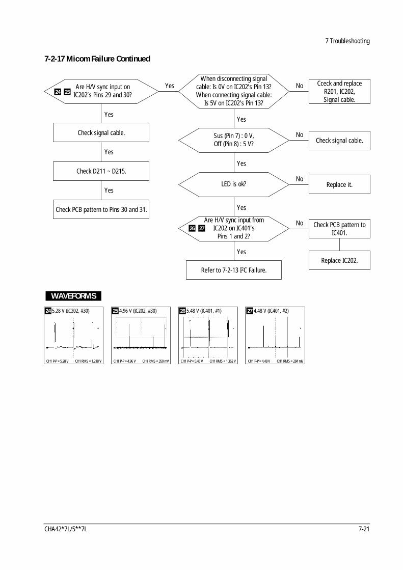
Are H/V sync input on IC202’s Pins 29 and 30?
Check the connection of signal cable.
Refer to 7-2-12 High Voltage Failure.
Yes
Check H/V sync input line.No
7-1-6 Misconvergence
Spec in?(Center : 0.3 mm, Cornor : 0.4 mm)
Readjust Misconvergence.
Done
Yes
Change CRT and readjustMiconvergence and color.
No
Refer to 7-2-17 MicomFailure.
No
Are H/V sync input on IC401’s Pins 1 and 2?
Yes
Check and replace IC401.
Yes
Check H/V sync input line.No
Check and replace IC202.No
WAVEFORMS
24
26
25
27
24 5.28 V (IC202, #30)
CH1 P-P = 5.28 V CH1 RMS = 1.218 V
25 4.96 V (IC202, #30)
CH1 P-P = 4.96 V CH1 RMS = 350 mV
26 5.48 V (IC401, #1)
CH1 P-P = 5.48 V CH1 RMS = 1.362 V
27 4.48 V (IC401, #2)
CH1 P-P = 4.48 V CH1 RMS = 284 mV

7 Troubleshooting
CHA42*7L/5**7L 7-5
7-1-7 Poor Focus
Improved Focus? Aging monitor and check focuschange for 1~2 hours.
Check Focus lead from FBT to CRT Socket.
Adjust Focus VR.
No
Yes
Are the CRT Socket and connection OK? Replace and connect it.
Check and replace CRT.
Yes
Yes
No
7-1-8 Purity Failure
Degaussing
Is purity OK? Done
No
Yes
IS degaussing circuit OK? Refer to 7-2-19 Degaussing Failure.
Yes
No
Check if there is strong electric or magnetic fields near
user’s circumstance?
Recommend free electric or magnetic field.
No
Yes
Change CRT and readjustmisconvergence and color.
7 Troubleshooting
7-6 CHA42*7L/5**7L
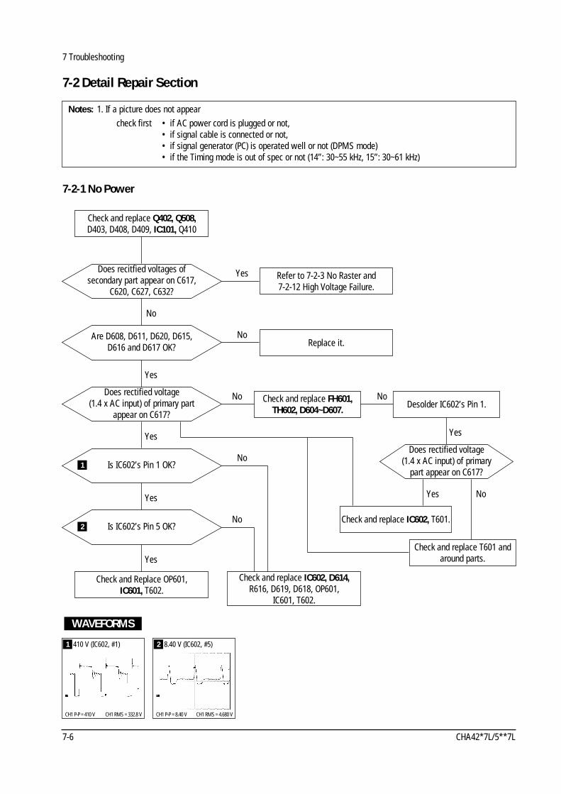
7-2 Detail Repair Section
Notes: 1. If a picture does not appearcheck first • if AC power cord is plugged or not,
• if signal cable is connected or not,• if signal generator (PC) is operated well or not (DPMS mode)• if the Timing mode is out of spec or not (14”: 30~55 kHz, 15”: 30~61 kHz)
Does recitfied voltages ofsecondary part appear on C617,
C620, C627, C632?
Refer to 7-2-3 No Raster and 7-2-12 High Voltage Failure.
Check and replace Q402, Q508, D403, D408, D409, IC101, Q410
Yes
Are D608, D611, D620, D615, D616 and D617 OK? Replace it.
Check and Replace OP601, IC601, T602.
Check and replace IC602, D614,R616, D619, D618, OP601,
IC601, T602.
No
No
Does rectified voltage (1.4 x AC input) of primary part
appear on C617?
Check and replace FH601, TH602, D604~D607.
Yes
Yes
No
Is IC602’s Pin 1 OK?No
Yes
Yes
Is IC602’s Pin 5 OK?
Yes
NoYes
Does rectified voltage (1.4 x AC input) of primary
part appear on C617?
No
7-2-1 No Power
Desolder IC602’s Pin 1.
Check and replace IC602, T601.
Check and replace T601 andaround parts.
No
WAVEFORMS
1
2
1 410 V (IC602, #1)
CH1 P-P = 410 V CH1 RMS = 332.8 V
2 8.40 V (IC602, #5)
CH1 P-P = 8.40 V CH1 RMS = 4.680 V

7 Troubleshooting
CHA42*7L/5**7L 7-7
Is LED blinking? (1 sec toggle) Check and replaceOP201, Q201.
Make sure that there is No H/V sync from signal generator. (Signal cable
should be connected)
Yes
Are there 5V on IC202’s Pin 7 (sus)and 0V on IC202’s Pin 8 (off)? Check and replace IC202.
Check and replace IC202.
No
Is OP201 OK?Yes
No
No
Yes
+12 V Off? Check and replace Q602, Q605, Q606.No
Yes
+6.3 V line Off? Check and replace Q603, Q604.
Done
No
Yes
7-2-2 DPMS Failure
7-2-2 (a) Off Mode (No H/V sync)

7 Troubleshooting
7-8 CHA42*7L/5**7L
7-2-2 (b) Suspend Mode (H sync: OK, V sync: No)
Is LED blinking? (0.5 sec toggle) Check and replaceOP201, Q201.
Make sure that H sync is OK and V sync isnot. (Signal cable should be connected)
Yes
Are there 5V on IC202’s Pin 7 (sus)and 5V on IC202’s Pin 8 (off)? Check and replace IC202.
Check and replace IC202.
No
Is OP201 OK?Yes
No
No
Yes
+12 V Off? Check and replace Q602, Q605, Q606.No
Yes
Done
7-2-2 (c) Stand-by Mode (H sync: No, V sync: OK)
Is LED blinking? (0.5 sec toggle) Check and replaceOP201, Q201.
Make sure that H sync is not and V sync isOK. (Signal cable should be connected)
Yes
Are there 0V on IC202’s Pin 7 (sus)and 5V on IC202’s Pin 8 (off)? Check and replace IC202.
Check and replace IC202.
No
Is OP201 OK?Yes
No
No
Yes
Is high voltage On? Refer to 7-2-3 No Raster and 7-2-12 High Voltage Failure.
No
Yes
Video Mute? Refer to 7-2-16 No Video and 7-2-13 I2C Failure.
No
Yes
Done

7 Troubleshooting
CHA42*7L/5**7L 7-9
7-2-3 No Raster : No Raster means (Power: OK, High Voltage: No)
Is 12 V on C629?Check and replaceQ605, Q602, Q606,
IC101, IC401.
Yes
Check signal cable and pattern.
No
Is 0 V on IC202’s Pin 7 (sus)?Yes
No
Check and replaceIC202.
Are H/V sync on IC202’s Pins 29 and 30?
Yes
No
Is 56 V on C517? Refer to 7-2-1 No Power.No
Yes
Does oscillation waveform appear on IC401’s Pin 6?
Check and replace C409, IC401, R406.
No
Yes
WAVEFORMS3
Does horizontal output waveformappear on IC401’s Pin 26?
Check and replace Q403, T401, Q402, T501, Q508.
No
Yes
4
Is Q402 OK? Replace it.No
Yes
Is Q508 OK? Replace it.
Check and replace D409, D408,D403, D515.
Check and replace IC401, Q403,T401, D503, D505, D519, C440, C407,
D216, Q203, T501, CRT.
No
Yes
Operating?
Yes
3 5.12 V (IC401, #6)
CH1 P-P = 5.12 V CH1 RMS = 4.256 V
4 4.60 V (IC401, #26)
CH1 P-P = 4.60 V CH1 RMS = 3.054 V
7 Troubleshooting
7-10 CHA42*7L/5**7L
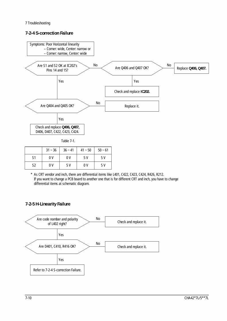
7-2-4 S-correction Failure
7-2-5 H-Linearity Failure
Are S1 and S2 OK at IC202’s Pins 14 and 15? Replace Q406, Q407.
Symptoms: Poor Horizontal linearity– Corner: wide, Center: narrow or– Corner: narrow, Center: wide
No
Are Q404 and Q405 OK? Replace it.
Check and replace Q406, Q407,D406, D407, C422, C423, C424.
Check and replace IC202.
Yes
Are Q406 and Q407 OK?No
Yes
No
Yes
31 ~ 36 36 ~ 41 41 ~ 50 50 ~ 61
S1 0 V 0 V 5 V 5 V
S2 0 V 5 V 0 V 5 V
Table 7-1.
* As CRT vendor and inch, there are differential items like L401, C422, C423, C424, R426, R212.If you want to change a PCB board to another one that is for different CRT and inch, you have to change differential items at schematic diagram.
Are code nomber and polarity of L402 right? Check and replace it.
No
Yes
Are D401, C410, R416 OK? Check and replace it.
Refer to 7-2-4 S-correction Failure.
No
Yes

7 Troubleshooting
CHA42*7L/5**7L 7-11
7-2-6 Invariable H_Size
Does the PWM duty of IC202’s Pin18 vary, pressing H_Size button?
Check and replaceQ409.
Yes
Is paravola waveform on IC401’s Pin 24? Replace IC401.
Replace IC202.
No
Is Q409 OK?No
No
No
Yes
Are Q410 and D408 OK? Replace it.No
Yes
Check and replace Q408, Q409, L402.
WAVEFORMS
8 8 1.12 V (IC401, #24)
CH1 P-P = 1.12 V CH1 RMS = 3.094 V
Does PWM duty of IC202’s Pin 22 vary with different timings?
(Low freq. : narrow duty High freq. : wide duty)
Check and replace IC202 and someparts around it.
Check if R444 and R434 are right as CRT differential items?
Adjust horizontal minium size withsoftjig. (Refer to 6-2-1)
No
Does the FBT B+ voltage on T501’sPin 2 vary with different timings? Refer to 7-2-12 High Voltage Failure.
Yes
No
Yes
7-2-7 Abnormal H_Size

7 Troubleshooting
7-12 CHA42*7L/5**7L
7-2-8 S_Pin, Trap, Para, V_Lin, Pin_Bal Failure
Is IC401’s Pin 24 OK?
Yes
Check and replace IC401.No
Does the PWM duty of IC202’s Pin 17 vary, pressing tilt
and + or – key?Check and replace IC302, IC202.
No
No
Does the output voltage of IC302’s Pin 1 vary, pressing tilt and
+ or – key?
Check and replace IC302, +13 V and –12 V line.
Check and replace CRT.
Yes
Refer to 7-2-13 I2C Failure.
No
Key check (7-2-19)
7-2-9 Tilt Failure
Check tilt connector. (CN303)
Key check (7-2-19)
WAVEFORMS
8
8 1.12 V (IC401, #24)
CH1 P-P = 1.12 V CH1 RMS = 3.094 V

7 Troubleshooting
CHA42*7L/5**7L 7-13
7-2-10 Vertical Deflection Failure
Are +13 V, –12 V line OK?
Is V_out waveform on IC401’s Pin 23?
Yes
Check and replace D616, D608,IC301, IC302.
No
Symptoms: – One horizontal line– Rainbow color, No Video
Check and replaceR314, R315, IC401.
No
Is V_deflection waveform onIC301’s Pin 5?
Check and replace IC301, R312, R310,and some parts around it.
Check and replace IC401.
Yes
Is 8 V on IC401’s Pin 21?No
Yes
No
Yes
Refer to 7-2-13 I2C Failure.
10
9
7-2-11 Invariable V_Size or V_Position
Key check (7-2-18)
Refer to 7-2-13 I2C Failure.
Does V_Out (IC401’s Pin 23) vary,pressing V_Size or V_Posi key?
Check and replace IC301 and someparts around it.
No
Yes
WAVEFORMS
10 50.8 V (IC301, #5)
CH1 P-P = 50.8 V CH1 RMS = 7.04 V
9 3.16 V (IC401, #23)
CH1 P-P = 3.16 V CH1 RMS = 3.686 V
9
WAVEFORMS
9 3.16 V (IC401, #23)
CH1 P-P = 3.16 V CH1 RMS = 3.686 V

7 Troubleshooting
7-14 CHA42*7L/5**7L
7-2-12 High Voltage Failure
Is Q508’s drain waveform ok? Check and replace it.No
Check and replace AFC input linefrom T501 to IC401’s Pin 12. :
D412, D413, C441, R401.
Yes
Are Q508, D515, L501 ok?No
Yes
Check and replace it.Are Q402, D409, D408, D403
and Q410 ok?No
Yes
Is 56 V on C617? Refer to 7-2-1 No Power.No
Yes
Does the PWM duty of IC202’s Pin16 vary with different H_freq.?
Check and replace IC202, Q203, D216.
No
Yes
WAVEFORMS
13
11
Are D503, D505, D519, R508, R506,R530, Q203, D216 and D415 ok? Check and replace it.
No
Yes
Does B_Out duty of IC401’s Pin 28 vary with different
H_frequency and image load (Full White or No Video)?
Check and replace IC401, Q507,Q509, T501 and REG_IN line to
IC401’s Pin 15.
No
Yes
Check and replace Q507, Q509,IC401, T501.
11
CH1 P-P = 5.12 V CH1 RMS = 4.256 V
12 14.0 V (IC401, #28)
CH1 P-P = 14.0 V CH1 RMS = 7.34 V
13 136 V (Q508, Drain)
CH1 P-P = 136 V CH1 RMS = 78.3 V
Symptoms 1: – No Power– No Raster – Unstable operation (Fixed FBT B+ voltage with different H_frequency,
Over 31 kHz: whistle sound, Narrow H_Size, Unsynchronized image, 31 kHz: OK)
12

7 Troubleshooting
CHA42*7L/5**7L 7-15
Are D505, C502, R506, R503 andC445 ok?
Yes
Check and replace it.No
Symptoms 2: – X-ray protection– One vertical line and then high voltage shut down.
Check and replace Q402, Q508,D409, D408, D403, IC401.
Check and replace Q203, IC202.
Is 5 V on IC401’s Pin 32 and IC203’s Pin 8? Check and replace it.
No
Yes
Is there data communication onIC401’s Pins 30 and 31?
No
Yes
Is there data communication on IC401’s Pins 30 and 31 duringI2C function? (H/V Posi, V_Size,
S_Pin, Trap, Cont, Brit)
Check I2C data and clock line.
Check and replace I2C devices. (IC101, IC401, IC203)
No
Yes
Done
14
14
7-2-13 I2C Failure
– Almost data (Horizontal drive duty, FBT B+ duty, display image data, color data) is transferred from IC203 to IC101 and IC401 through I2C data line during power on.
– After user adjusts display image data, contrast and brightness data, these are saved to IC203.
Key check (7-2-18)WAVEFORMS
14 5.92 V (IC203, #5, 6)
CH1 P-P = 5.92 V CH1 RMS = 3.812 V
CH1 : IC401’s Pin 31CH2 : IC401’s Pin 30

7 Troubleshooting
7-16 CHA42*7L/5**7L
Are full white and whitesquare luminance almost
same?
No
No
Does full white luminance vary,adjusting ABL step with Softjig?
Yes
Is R121 right as CRT’sdifferential items?
Yes
No
Yes
Does the voltage of IC101’s Pin 8 vary between full
white and No Video?
Yes
No
Does the PWM duty of IC202’s Pin 21 vary adjusting
ABL step?
Yes
No
Display the full white pattern.
Replace it.
Check and replace IC101.
Does T501’s Pin 8 voltage vary between full white
and No Video?
Yes
No
Check and replace D518, IC101.
Are 12 V line, R504, L504, Q501and Q518 ok?
No
Yes
Replace it.
Are C509, D514, Q502 and Q506ok?
No
Yes
Replace it.
Check and replace T501 and CRT.
Check and replace IC202 andaround parts.
Replace R121 to higher or lowerone that meets the spec.
Check connections betweenCN202 and CN202_2.
7-2-14 ABL Failure
Symptoms : – Full white luminance is too bright. (ABL minium is over 35 F/L)– Full white luminance is too dark. (ABL maximum is under 35 F/L)– The luminance of full white and No Video are almost same.
F/W: 4.1~4.3VNo Video: 5.3~6.0V
F/W: 1.5~3.0VNo Video: 5.5~7.0V

7 Troubleshooting
CHA42*7L/5**7L 7-17
Does IC101’s output (Pins 18, 21 and 23) vary, pressing
cont, brit key?Replace IC101.
Yes
Yes
No
Does IC102’s output (Pins 1, 3 and 5) vary, pressing
cont, brit key?Replace IC102.
Yes
No
Check and replace Q101R, Q101G,Q101B, Q102R, Q102G, Q102B,
Q103R, Q103G, Q103B.
Refer to 7-2-18 Key Check.(Contrast, Brightness)
I2C check (7-2-13)
7-2-15 Invariable Contrast, Brightness Control
15
16
WAVEFORMS
15 3.16 V (IC101, #21)
CH1 P-P = 3.16 V CH1 RMS = 1.008 V
16 43.2 V (IC102, #3)
CH1 P-P = 43.2 V CH1 RMS = 63.56 V

7 Troubleshooting
7-18 CHA42*7L/5**7L
7-2-16 No Video
Is heater voltage (5.9~6.3V) onSK103’s heater Pin? Replace it.
No
Check and replace Q604, R621.
Yes
Are D617, Q603 and R631 ok?No
Yes
Check and replaceQ603, R624, R625.
Is 0V on Q604’s collector?No
Yes
Check and replaceIC202.
Is 5V on IC202’s Pin 8No
Yes
Replace IC101.
Refer to 7-2-1 No Power.
Opening BD102, is it short between IC101’s Vcc and
ground?
No
Yes
Check signal cable connection.Check Cont, Brit key (All max).
Is G1 voltage OK at SK103’s G1 Pin?
Check and replace SK102, C119,Q504, D510, R513, R521, R520,
D513, T501.
Check CN103’s connection (G2).
No
Yes
WAVEFORMS17
Desoldering SK101 and C118, is G2 voltage ok?
Check and replace SK101, C118and then T501.
No
Yes
Is 12 V on IC101’s Pins 1 and 7?No
Check and replaceIC202 and around it.
Is clamp signal on IC101’s Pin 12?
NoIs IC101’s output on Pins 18, 21 and 23?
No
Yes
17 35.2 V (SK103, G1)
CH1 P-P = 35.2 V CH1 RMS = 80.84 V
15 18

7 Troubleshooting
CHA42*7L/5**7L 7-19
Check and replaceIC202 and around it.
Is clamp signal on IC101’s Pin 12?
NoIs IC101’s output on Pins 18, 21 and 23?
No15 18
Refer to 7-2-15 ABL Failure.
YesYes
Check 75 V line.Is 75 V on IC102’s Pin 6?NoIs IC102’s output on Pins 1,
3 and 5?No
16
Replace IC102.
YesYes
Check again cont, brit key.6.3 V line, G1, G2 line.
Is it ok?
Are there waveforms on SK103’sR, G, B?
Yes
Disconnect Video PCB from CRT neck.
YesNo
Replace IC101.
7-2-16 No Video Continued
Are ther waveforms on SK103’s R, G, B? Check and replace SK103 and CRT.
No
Yes
Check and replace Q101R, Q101G,Q101B, Q102R, Q102G, Q102B,
D103R, D103G, D103B and PCB pattern.
19
WAVEFORMS
15 3.16 V (IC101, #21)
CH1 P-P = 3.16 V CH1 RMS = 1.008 V
16 43.2 V (IC102, #3)
CH1 P-P = 43.2 V CH1 RMS = 63.56 V
18 5.60 V (IC101, #12)
CH1 P-P = 5.60 V CH1 RMS = 4.908 V
19 46.4 V (SK103, G)
CH1 P-P = 46.4 V CH1 RMS = 38.16 V

7 Troubleshooting
7-20 CHA42*7L/5**7L
Check if timing is out of spec or not.
Key check (all key) : Refer to 7-2-19.
Check the connection of signal cable. If signal cable is disconnected, self raster (No Video, Bright Raster) appears.
If there is no H/V sync, monitor is operated as DPMS mode.
If out of sepc, monitor is operated as stand-by mode. (No Video, LED: 0.5 sec toggle)14”: Horizontal 30 ~ 55 kHz, Vertical 50 ~ 125 Hz15”: Horizontal 30 ~ 61 kHz, Vertical 50 ~ 125 Hz
Check H/V sync from PC or signalgenerator.
Are oscillation (8 MHz) on IC202’s Pins 34 and 35? Check and replace X201, C205 ,C206.
Yes
No
7-2-17 Micom Failure
Refer to 7-2-1 No Power.
Is 13 V on C627?No
Is 5V on IC202’s Pins 9 and 35?No
Cceck and replaceR201, IC202, Signal cable.
When disconnecting signal cable: Is 0V on IC202’s Pin 13?When connecting signal cable:
Is 5V on IC202’s Pin 13?
NoAre H/V sync input on IC202’s Pins 29 and 30?
Yes
20
Check reset part.Are Q204, C223 and R210 ok? Replace it.
Yes
No
Check power key (IC202’s Pin 2).Normal : 5 V, Pressing key : 0 V Check and replace SW211, IC202.
Yes
No
Check and replace IC603.
YesYes
24 25
WAVEFORMS
20 4.92 V (IC202, #33)
CH1 P-P = 4.92 V CH1 RMS = 2.912 V
7 Troubleshooting
CHA42*7L/5**7L 7-21
Cceck and replaceR201, IC202, Signal cable.
When disconnecting signal cable: Is 0V on IC202’s Pin 13?When connecting signal cable:
Is 5V on IC202’s Pin 13?
NoAre H/V sync input on IC202’s Pins 29 and 30?
Yes24 25
7-2-17 Micom Failure Continued
Check signal cable. Sus (Pin 7) : 0 V, Off (Pin 8) : 5 V?
No
Refer to 7-2-13 I2C Failure.
Check signal cable.
Replace it.
Yes
LED is ok?No
Yes
Check PCB pattern toIC401.
Replace IC202.
Are H/V sync input from IC202 on IC401’s
Pins 1 and 2?
No
Yes
Yes
Yes
Check D211 ~ D215.
Check PCB pattern to Pins 30 and 31.
Yes
Yes
WAVEFORMS
24 5.28 V (IC202, #30)
CH1 P-P = 5.28 V CH1 RMS = 1.218 V
25 4.96 V (IC202, #30)
CH1 P-P = 4.96 V CH1 RMS = 350 mV
26 5.48 V (IC401, #1)
CH1 P-P = 5.48 V CH1 RMS = 1.362 V
27 4.48 V (IC401, #2)
CH1 P-P = 4.48 V CH1 RMS = 284 mV
26 27

CH1 of Picture Pin 21
Pressed RMS voltage
0.7 ~ 0.9 V
0.7 ~ 0.9 VCH2 of Picture Pin 21
Keyout
Normal
5 V
0 VKeyin
7 Troubleshooting
7-22 CHA42*7L/5**7L
7-2-18 Key Check
1) Key Map
R241 R242 R243 R244 R245 R246 R247
SW204(V-Size)
SW203(H-Size)
SW202(V-Posi)
SW201(H-Posi)
SW208(Cont)
SW207(Brit)
SW206(Trap)
SW209(Up)
SW210(Down)
SW205(S-Pin)
Keyout3(#5)
Keyout2(#4)
Keyout1(#3)
Keyin4(#39)
Keyin3(#40)
Keyin2(#42)
Keyin1(#1)
2) Voltage Check of Keyin and Keyout– Press the key what you want to check.– At that moment, the voltage of keyin and keyout that is connected with together should be changed as follows.
3) LED Check– Pressing key, LED should be blinked.
4) How to Repair?– If only one key has a key problem, replace that key.– But if some keys that are connected with same keyin or keyout line have problems,
check and replace PCB pattern and IC202.
WAVEFORMS
21 5.52 V (IC203, Keyout)
CH1 P-P = 5.52 V CH1 RMS = 3.696 V
21 5.44 V (IC203, Keyin)
CH1 P-P = 5.44 V CH1 RMS = 1.436 V
7 Troubleshooting
CHA42*7L/5**7L 7-23
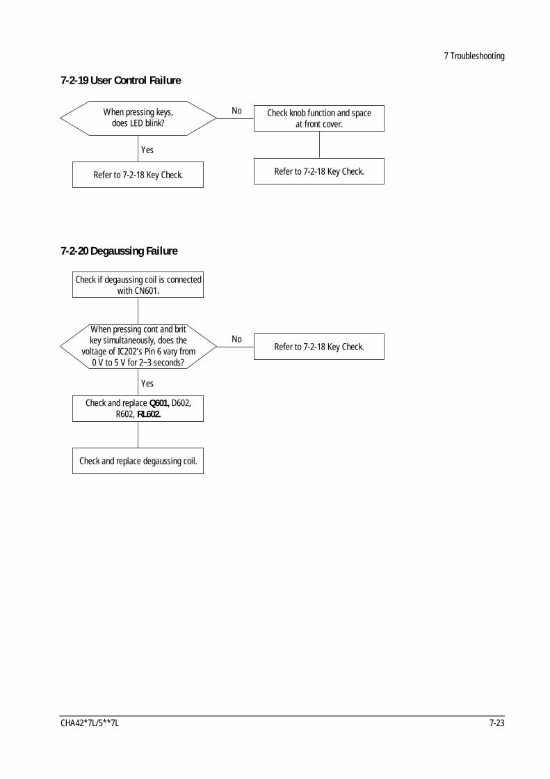
7-2-19 User Control Failure
When pressing keys, does LED blink?
Check knob function and space at front cover.
Refer to 7-2-18 Key Check.Refer to 7-2-18 Key Check.
Yes
No
When pressing cont and brit key simultaneously, does the
voltage of IC202’s Pin 6 vary from0 V to 5 V for 2~3 seconds?
Refer to 7-2-18 Key Check.
Check if degaussing coil is connectedwith CN601.
Check and replace Q601, D602, R602, RL602.
No
Yes
Check and replace degaussing coil.
7-2-20 Degaussing Failure

7 Troubleshooting
7-24 CHA42*7L/5**7L
7-2-21 Horizontal Blank Failure
7-2-23 Spot at Center During Power Off
7-2-22 Whistle Sound
Check trans coil (L401, T501, T601, CRT)
Is H_Blank waveform on Q510’s collector? Check CN202 and CN202_2.
Check and replace IC101.
Check and replace C503, C516, R540, C515.
No
Yes
Are Q504 and D517 ok? Replace it.
Yes
No
Symptoms: – Dark image and if shifting image to left or right side, image is rolled.– Raster left or right side is rolled.
Does G1 voltage vary from –60~80 Vrms to –200 Vrms during
power off time? (After falling down to –200V, G1 voltage is
slowly increased to 0V).
Check and replace CRT.
No
Yes32
31
Are 12 V line and Q504 ok? Replace it.
Check and replace D510, R513, R521, R520, C518.
Yes
No
WAVEFORMS
31 5.36 V (Q510, Collector)
CH1 P-P = 5.36 V CH1 RMS = 4.210 V
WAVEFORMS
32 158 V (CN202, G1)
CH1 P-P = 158 V CH1 RMS = 151.1 V

BD101 3301-000011 CORE-FERRITE BEAD AA,3.5x1.0x5.7mm,1500BD102 3301-000011 CORE-FERRITE BEAD AA,3.5x1.0x5.7mm,1500BD104 3301-000011 CORE-FERRITE BEAD AA,3.5x1.0x5.7mm,1500BD105 3301-000011 CORE-FERRITE BEAD AA,3.5x1.0x5.7mm,1500BD401 3301-000011 CORE-FERRITE BEAD AA,3.5x1.0x5.7mm,1500BD403 3301-000011 CORE-FERRITE BEAD AA,3.5x1.0x5.7mm,1500BD404 3301-000011 CORE-FERRITE BEAD AA,3.5x1.0x5.7mm,1500BD405 3301-000012 CORE-FERRITE BEAD AA,3.5x1x9mm,1000,3000BD406 3301-000012 CORE-FERRITE BEAD AA,3.5x1x9mm,1000,3000BD407 3301-000011 CORE-FERRITE BEAD AA,3.5x1.0x5.7mm,1500BD502 3301-000011 CORE-FERRITE BEAD AA,3.5x1.0x5.7mm,1500BD603 3301-000011 CORE-FERRITE BEAD AA,3.5x1.0x5.7mm,1500BD604 3301-000011 CORE-FERRITE BEAD AA,3.5x1.0x5.7mm,1500BD605 3301-000011 CORE-FERRITE BEAD AA,3.5x1.0x5.7mm,1500BD608 3301-000011 CORE-FERRITE BEAD AA,3.5x1.0x5.7mm,1500BD610 3301-000011 CORE-FERRITE BEAD AA,3.5x1.0x5.7mm,1500BD611 3301-000012 CORE-FERRITE BEAD AA,3.5x1x9mm,1000,3000C101B 287.3 134.5 2401-000028 C-AL 10uF,20%,50V,GP,5x11mm,5mm,TPC101G 281.0 134.5 2401-000028 C-AL 10uF,20%,50V,GP,5x11mm,5mm,TPC101R 277.5 137.0 2401-000028 C-AL 10uF,20%,50V,GP,5x11mm,5mm,TPC103B 295.3 200.0 2301-000010 C-FILM,PEF 100nF,5%,100V,11.5x12.5mm,5mmC103G 277.0 204.0 2301-000010 C-FILM,PEF 100nF,5%,100V,11.5x12.5mm,5mmC103R 295.3 236.3 2301-000010 C-FILM,PEF 100nF,5%,100V,11.5x12.5mm,5mmC104B 318.5 193.0 2202-002009 C-CERAMIC,MLC-AXIAL 100nF,+80-20%,50V,Y5V,2.3X3.0C104G 323.8 216.0 2202-002009 C-CERAMIC,MLC-AXIAL 100nF,+80-20%,50V,Y5V,2.3X3.0C104R 323.8 228.3 2202-002009 C-CERAMIC,MLC-AXIAL 100nF,+80-20%,50V,Y5V,2.3X3.0C106B 323.5 141.3 2401-000043 C-AL 1uF,20%,160V,GP,6.3x11mm,5mm,TC106G 324.0 187.3 2401-000043 C-AL 1uF,20%,160V,GP,6.3x11mm,5mm,TC106R 315.0 186.8 2401-000043 C-AL 1uF,20%,160V,GP,6.3x11mm,5mm,TC107 258.0 229.8 2305-000004 C-FILM,MPEF 220nF,10%,100V,TP,12.7x16,5mC110 266.3 236.5 2202-002009 C-CERAMIC,MLC-AXIAL 100nF,+80-20%,50V,Y5V,2.3X3.0C111 252.5 239.0 2401-000042 C-AL 100uF,20%,16V,GP,6.3x7mm,2.5mmC112 266.3 204.5 2202-002009 C-CERAMIC,MLC-AXIAL 100nF,+80-20%,50V,Y5V,2.3X3.0C113 249.5 226.5 2401-000033 C-AL 100uF,20%,100V,GP,13x20mm,5mmC114 305.8 236.8 2401-000043 C-AL 1uF,20%,160V,GP,6.3x11mm,5mm,TC115 280.5 153.0 2202-002009 C-CERAMIC,MLC-AXIAL 100nF,+80-20%,50V,Y5V,2.3X3.0C116 284.5 157.0 2401-000042 C-AL 100uF,20%,16V,GP,6.3x7mm,2.5mmC117 269.5 153.0 2202-002009 C-CERAMIC,MLC-AXIAL 100nF,+80-20%,50V,Y5V,2.3X3.0C118 316.8 167.3 2201-000154 C-CERAMIC,DISC 10nF,+80-20%,2KV,Y5P,20x5,10,TC119 265.0 166.5 2201-000019 CAP-CERAMIC,103Z,2H,DISC 10NF,500V,80-20%,Y5V,RADIALC120 292.8 153.0 2202-002009 C-CERAMIC,MLC-AXIAL 100nF,+80-20%,50V,Y5V,2.3X3.0C121 275.0 153.0 2202-002009 C-CERAMIC,MLC-AXIAL 100nF,+80-20%,50V,Y5V,2.3X3.0C122 269.0 226.0 2201-000502 C-CERAMIC,DISC 39pF,5%,50V,NPO,5x3.5,5,TPC123 288.0 137.8 2202-002009 C-CERAMIC,MLC-AXIAL 100nF,+80-20%,50V,Y5V,2.3X3.0C124 293.5 134.5 2401-000042 C-AL 100uF,20%,16V,GP,6.3x7mm,2.5mm
!
CHA42*7L/5**7L 9-1
Loc. No. Coordinates (X,Y) Code No. Description Specification Remarks
9 Electrical Parts List9-1 Main PCB Parts

C125 253.3 188.3 2201-000021 C-CERAMIC,DISC 100nF,+80-20%,50V,Y5V,8x3,5,TPC126 323.5 174.0 2202-002009 C-CERAMIC,MLC-AXIAL 100nF,+80-20%,50V,Y5V,2.3X3.0C127 304.8 137.3 2401-000027 C-AL 4.7uF,20%,50V,GP,5x11mm,5mm,TPC201 44.3 93.3 2401-000023 (T)50V 1M CAP-AL.ELEC,105M,1HC203 51.3 75.5 2201-000017 C-CERAMIC,DISC 1nF,10%,50V,Y5P,4x3.5,5,TPC204 47.8 75.5 2201-000146 C-CERAMIC,DISC 100pF,5%,50V,SL,5x3.5,5,TPC205 44.3 75.5 2201-000009 C-CERAMIC,DISC 22pF,5%,50V,NPO,4x3.5,5,TPC206 40.5 75.5 2201-000397 C-CERAMIC,DISC 24pF,5%,50V,CH,TP,5.0x3.0C207 70.5 31.0 2401-000050 C-AL 10uF,20%,16V,GP,5x11mm,2mm,TPC208 2202-002009 C-CERAMIC,MLC-AXIAL 100nF,+80-20%,50V,Y5C210 58.0 43.0 2202-002009 C-CERAMIC,MLC-AXIAL 100nF,+80-20%,50V,Y5V,2.3X3.0C211 55.3 43.0 2202-002009 C-CERAMIC,MLC-AXIAL 100nF,+80-20%,50V,Y5V,2.3X3.0C212 2401-000023 (T)50V 1M CAP-AL.ELEC,105M,1H TILT OPTIONC219 210.5 102.3 2201-000011 C-CERAMIC,DISC 47pF,5%,50V,NPO,6.5x3.0,5,TPC220 77.8 85.8 2401-000050 C-AL 10uF,20%,16V,GP,5x11mm,2mm,TPC221 33.8 42.0 2202-002009 C-CERAMIC,MLC-AXIAL 100nF,+80-20%,50V,Y5V,2.3X3.0C222 68.8 13.5 2401-000023 (T)50V 1M CAP-AL.ELEC,105M,1HC223 33.8 109.5 2401-000027 C-AL 4.7uF,20%,50V,GP,5x11mm,5mm,TPC301 110.0 91.3 2305-001009 C-FILM,MPEF 39nF,5%,250V,13x9x4.5mm,7.5mmC304 107.0 73.5 2401-000023 (T)50V 1M CAP-AL.ELEC,105M,1HC305 106.5 41.8 2305-000280 (T)63V 224K CAP-MPETP,224K,1J,5PC306 140.8 41.3 2401-000039 C-AL 1000uF,20%,16V,GP,10x16mm,5mmC307 106.0 66.3 2401-000849 (T)35V 220M CAP-AL.ELEC,227M,1VC309 102.5 54.0 2201-000013 C-CERAMIC,DISC 470pF,10%,50V,Y5P,4x3.5,5,TPC310 106.5 56.5 2301-000012 (T)100V 222J CAP-MYLAR,222J,2A,5PC311 101.5 50.1 2301-000015 C-FILM,PEF 10nF,5%,100V,7x3.2x7mm,5mm,TPC312 2305-000001 C-FILM,MPEF 470nF,10%,63V,TP,6.0X15.5X7 TILT OPTIONC401 49.0 142.3 2401-000027 C-AL 4.7uF,20%,50V,GP,5x11mm,5mm,TPC402 54.0 143.3 2305-000280 C-FILM,MPEF 220nF,10%,63V,TP,7.5x13.5mmC403 52.3 134.3 2301-000174 C-FILM,PEF 15nF,5%,100V,7.2x4.0x7.5mm,5mmC404 63.0 142.3 2401-000031 C-AL 47uF,20%,16V,GP,6.3x11mm,5mm,TC405 63.5 134.3 2202-002009 C-CERAMIC,MLC-AXIAL 100nF,+80-20%,50V,Y5V,2.3X3.0C406 57.8 137.3 2301-000257 C-FILM,PEF 4.7nF,10%,100V,5.8x12.5mm,5mmC407 69.0 142.5 2201-000471 C-CERAMIC,DISC 330pF,10%,50V,Y5P,4x3.5,5,TPC408 48.0 130.8 2301-000016 C-FILM,PEF 22nF,5%,100V,7.2x4.5x9.0mm,5mmC409 42.8 136.5 2202-002021 C-CERAMIC,MLC-RADIAL 1nF,5%,50V,NPO,TP,5.1x6.4x3.2C410 76.5 208.5 2201-000291 C-CERAMIC,DISC 1nF,10%,500V,Y5P,8.5x5MM,5,TPC411 100.0 228.5 2401-000876 (T)50V 220M CAP-AL.ELEC,227M,1HC412 82.0 199.3 2401-000048 (T)25V 47M CAP-AL.ELEC,476M,1EC413 71.8 179.0 2301-000012 (T)100V 222J CAP-MYLAR,222J,2A,5PC414 111.8 237.8 2301-001207 C-FILM,PPF 5.2nF,5%,2.5KV,BK,29x21.5x13. 15” C414 2303-000282 C-FILM,PPF 6nF,5%,1.6KV,TP,29*23*8.5,20m 14” C415 36.5 143.8 2201-000011 C-CERAMIC,DISC 47pF,5%,50V,NPO,6.5x3.0,5,TPC416 162.5 241.0 2401-000028 C-AL 10uF,20%,50V,GP,5x11mm,5mm,TPC417 132.8 229.0 2301-000133 C-FILM,PEF 10nF,10%,100V,6.5x12.5mm,5mm,TC418 177.0 241.0 2401-000028 C-AL 10uF,20%,50V,GP,5x11mm,5mm,TPC420 48.0 180.5 2401-000023 (T)50V 1M CAP-AL.ELEC,105M,1H
!
!
!
9 Electrical Parts List
9-2 CHA42*7L/5**7L
Loc. No. Coordinates (X,Y) Code No. Description Specification Remarks

C421 75.0 137.5 2201-000643 C-CERAMIC,DISC 680pF,10%,50V,Y5P,4x3.5,5,TPC422 43.8 218.3 2306-000137 C-FILM,MPPF 180nF,5%,250V,TP,19x16.5x8,7 15”C422 2306-000171 C-FILM,MPPF 270nF,5%,250V,TP,21.5x12.5mm 14”C423 55.5 218.0 2301-001162 C-FILM,MPPF 370nF,5%,250V,TP,19x18.5x12.5 15”C423 2301-001125 C-FILM,MPPF 600nF,5%,250V,TP,26x20x11.5, 14”C424 33.5 211.0 2301-001125 C-FILM,MPPF 600nF,5%,250V,TP,26x20x11.5,20 15”C424 2306-000249 C-FILM,MPPF 680nF,5%,250V,TP,26x20.5x12 14”C425 36.3 161.3 2401-000042 C-AL 100uF,20%,16V,GP,6.3x7mm,2.5mmC427 60.0 167.3 2301-000168 C-FILM,PEF 150nF,5%,100V,11.5x19mm,7.5mmC428 26.0 222.5 2401-000023 (T)50V 1M CAP-AL.ELEC,105M,1HC429 15.5 222.5 2401-000023 (T)50V 1M CAP-AL.ELEC,105M,1HC430 61.5 161.0 2305-000001 C-FILM,MPEF 470nF,10%,63V,6.0X15.5X7.5,5mmC431 36.3 168.5 2401-000042 C-AL 100uF,20%,16V,GP,6.3x7mm,2.5mmC434 72.8 168.5 2401-001509 C-AL 47uF,20%,16V,GP,6.3x7mm,2.5mmC435 151.8 122.0 2401-001012 C-ALUMINUM 3.3UF,20%,50V,BP,16+26.7,7.5mm,TC436 129.0 188.0 2303-001029 C-FILM,PPF 5.2nF,5%,630V,19x7x13,7.5,TPC437 155.5 147.0 2301-000012 (T)100V 222J CAP-MYLAR,222J,2A,5PC439 158.8 137.8 2201-000010 CAP-CERAMIC,330J,1H,NPO 33PF,50V,5%,NPOPPM,NPO,DISC-RADC440 77.5 132.3 2301-000016 C-FILM,PEF 22nF,5%,100V,7.2x4.5x9.0mm,5mmC441 185.0 135.5 2301-000012 (T)100V 222J CAP-MYLAR,222J,2A,5PC442 81.0 115.0 2201-000326 C-CERAMIC,DISC 2.2nF,10%,50V,Y5P,6.3X3.0,5,TPC443 37.5 137.3 2301-000016 C-FILM,PEF 22nF,5%,100V,7.2x4.5x9.0mm,5mmC445 50.5 172.3 2202-002009 C-CERAMIC,MLC-AXIAL 100nF,+80-20%,50V,Y5V,2.3X3.0C501 92.5 167.0 2202-002009 C-CERAMIC,MLC-AXIAL 100nF,+80-20%,50V,Y5V,2.3X3.0C502 103.0 147.3 2401-000966 C-AL 22uF,20%,50V,GP,6.3x11mm,5mm,TC503 191.0 136.3 2201-000017 C-CERAMIC,DISC 1nF,10%,50V,Y5P,4x3.5,5,TPC504 85.5 174.5 2202-002009 C-CERAMIC,MLC-AXIAL 100nF,+80-20%,50V,Y5V,2.3X3.0C505 110.8 159.3 2305-000004 C-FILM,MPEF 220nF,10%,100V,12.7x16,5mm,TPC506 77.3 31.0 2401-000050 C-AL 10uF,20%,16V,GP,5x11mm,2mm,TPC507 219.0 205.3 2201-000017 C-CERAMIC,DISC 1nF,10%,50V,Y5P,4x3.5,5,TPC508 207.5 144.5 2401-000046 (T)250V 10M CAP-AL.ELEC,106M,2EC509 194.8 241.0 2401-001334 C-AL 470nF,20%,50V,GP,5x11mm,2mm,TPC511 118.5 149.3 2201-000469 C-CERAMIC,DISC 330pF,10%,500V,Y5P,6x3.5,5,TPC512 130.0 137.5 2306-000007 C-FILM,MPPF 470nF,5%,250V,26.5x14mm,22.5mmC515 186.8 125.8 2201-000017 C-CERAMIC,DISC 1nF,10%,50V,Y5P,4x3.5,5,TPC516 186.8 129.5 2201-000471 C-CERAMIC,DISC 330pF,10%,50V,Y5P,4x3.5,5,TPC517 155.5 87.5 2401-000373 C-AL 100uF,20%,63V,GP,10x20mm,5mm,TC518 174.8 137.5 2401-000027 C-AL 4.7uF,20%,50V,GP,5x11mm,5mm,TPC519 234.3 165.3 2401-000010 C-AL 220uF,20%,16V,GP,6.3x11mm,2.5mC520 214.3 224.5 2202-002008 C-CERAMIC,MLC-AXIAL 10nF,+80-20%,50V,Y5V,2.3X3.0C601 34.0 13.5 2401-000039 C-AL 1000uF,20%,16V,GP,10x16mm,5mmC604 263.5 62.8 2201-000023 C-CERAMIC,DISC 2.2nF,20%,125V,Y5U,11x7,5,TPC605 269.0 45.3 2201-000023 C-CERAMIC,DISC 2.2nF,20%,125V,Y5U,11x7,5,TPC606 267.5 36.5 2301-001156 C-FILM,MPEF 220nF,10%,275V,BK,26x18x8.5,22C610 168.0 14.0 2301-000012 (T)100V 222J CAP-MYLAR,222J,2A,5PC611 176.3 23.3 2301-000287 (T)100V 562J CAP-MYLAR,562J,2A,5PC612 138.0 87.5 2401-000887 C-AL 220uF,20%,63V,GP,10x20mm,5mm,T !
!
!
!
9 Electrical Parts List
CHA42*7L/5**7L 9-3
Loc. No. Coordinates (X,Y) Code No. Description Specification Remarks
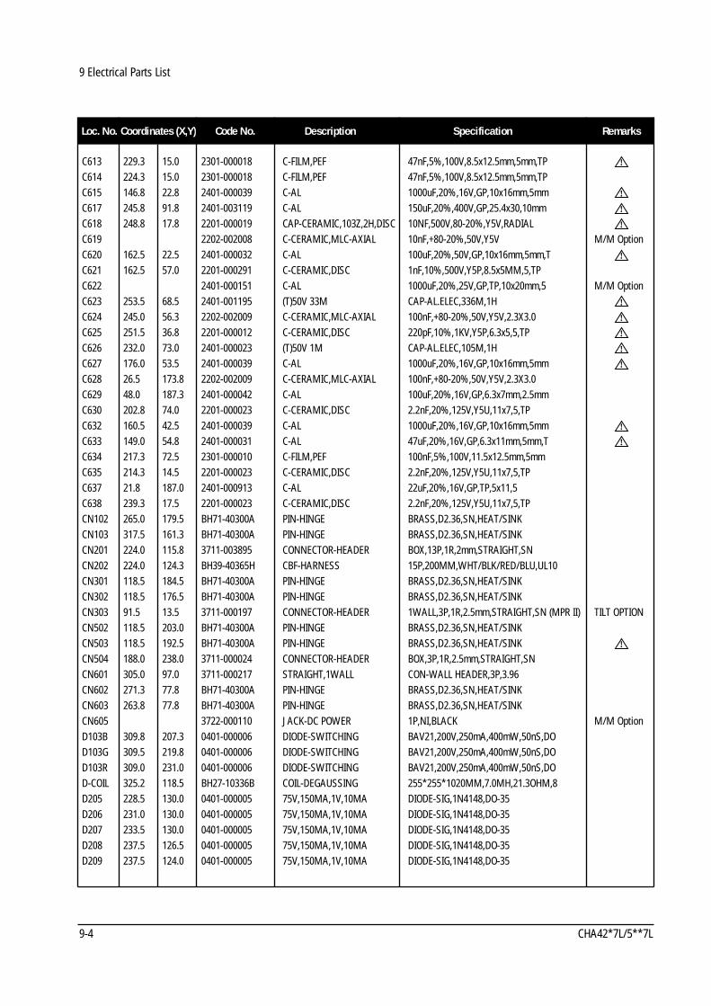
C613 229.3 15.0 2301-000018 C-FILM,PEF 47nF,5%,100V,8.5x12.5mm,5mm,TPC614 224.3 15.0 2301-000018 C-FILM,PEF 47nF,5%,100V,8.5x12.5mm,5mm,TPC615 146.8 22.8 2401-000039 C-AL 1000uF,20%,16V,GP,10x16mm,5mmC617 245.8 91.8 2401-003119 C-AL 150uF,20%,400V,GP,25.4x30,10mmC618 248.8 17.8 2201-000019 CAP-CERAMIC,103Z,2H,DISC 10NF,500V,80-20%,Y5V,RADIALC619 2202-002008 C-CERAMIC,MLC-AXIAL 10nF,+80-20%,50V,Y5V M/M OptionC620 162.5 22.5 2401-000032 C-AL 100uF,20%,50V,GP,10x16mm,5mm,TC621 162.5 57.0 2201-000291 C-CERAMIC,DISC 1nF,10%,500V,Y5P,8.5x5MM,5,TPC622 2401-000151 C-AL 1000uF,20%,25V,GP,TP,10x20mm,5 M/M OptionC623 253.5 68.5 2401-001195 (T)50V 33M CAP-AL.ELEC,336M,1HC624 245.0 56.3 2202-002009 C-CERAMIC,MLC-AXIAL 100nF,+80-20%,50V,Y5V,2.3X3.0C625 251.5 36.8 2201-000012 C-CERAMIC,DISC 220pF,10%,1KV,Y5P,6.3x5,5,TPC626 232.0 73.0 2401-000023 (T)50V 1M CAP-AL.ELEC,105M,1HC627 176.0 53.5 2401-000039 C-AL 1000uF,20%,16V,GP,10x16mm,5mmC628 26.5 173.8 2202-002009 C-CERAMIC,MLC-AXIAL 100nF,+80-20%,50V,Y5V,2.3X3.0C629 48.0 187.3 2401-000042 C-AL 100uF,20%,16V,GP,6.3x7mm,2.5mmC630 202.8 74.0 2201-000023 C-CERAMIC,DISC 2.2nF,20%,125V,Y5U,11x7,5,TPC632 160.5 42.5 2401-000039 C-AL 1000uF,20%,16V,GP,10x16mm,5mmC633 149.0 54.8 2401-000031 C-AL 47uF,20%,16V,GP,6.3x11mm,5mm,TC634 217.3 72.5 2301-000010 C-FILM,PEF 100nF,5%,100V,11.5x12.5mm,5mmC635 214.3 14.5 2201-000023 C-CERAMIC,DISC 2.2nF,20%,125V,Y5U,11x7,5,TPC637 21.8 187.0 2401-000913 C-AL 22uF,20%,16V,GP,TP,5x11,5C638 239.3 17.5 2201-000023 C-CERAMIC,DISC 2.2nF,20%,125V,Y5U,11x7,5,TPCN102 265.0 179.5 BH71-40300A PIN-HINGE BRASS,D2.36,SN,HEAT/SINKCN103 317.5 161.3 BH71-40300A PIN-HINGE BRASS,D2.36,SN,HEAT/SINKCN201 224.0 115.8 3711-003895 CONNECTOR-HEADER BOX,13P,1R,2mm,STRAIGHT,SNCN202 224.0 124.3 BH39-40365H CBF-HARNESS 15P,200MM,WHT/BLK/RED/BLU,UL10CN301 118.5 184.5 BH71-40300A PIN-HINGE BRASS,D2.36,SN,HEAT/SINKCN302 118.5 176.5 BH71-40300A PIN-HINGE BRASS,D2.36,SN,HEAT/SINKCN303 91.5 13.5 3711-000197 CONNECTOR-HEADER 1WALL,3P,1R,2.5mm,STRAIGHT,SN (MPR II) TILT OPTIONCN502 118.5 203.0 BH71-40300A PIN-HINGE BRASS,D2.36,SN,HEAT/SINKCN503 118.5 192.5 BH71-40300A PIN-HINGE BRASS,D2.36,SN,HEAT/SINKCN504 188.0 238.0 3711-000024 CONNECTOR-HEADER BOX,3P,1R,2.5mm,STRAIGHT,SNCN601 305.0 97.0 3711-000217 STRAIGHT,1WALL CON-WALL HEADER,3P,3.96CN602 271.3 77.8 BH71-40300A PIN-HINGE BRASS,D2.36,SN,HEAT/SINKCN603 263.8 77.8 BH71-40300A PIN-HINGE BRASS,D2.36,SN,HEAT/SINKCN605 3722-000110 JACK-DC POWER 1P,NI,BLACK M/M OptionD103B 309.8 207.3 0401-000006 DIODE-SWITCHING BAV21,200V,250mA,400mW,50nS,DOD103G 309.5 219.8 0401-000006 DIODE-SWITCHING BAV21,200V,250mA,400mW,50nS,DOD103R 309.0 231.0 0401-000006 DIODE-SWITCHING BAV21,200V,250mA,400mW,50nS,DOD-COIL 325.2 118.5 BH27-10336B COIL-DEGAUSSING 255*255*1020MM,7.0MH,21.3OHM,8D205 228.5 130.0 0401-000005 75V,150MA,1V,10MA DIODE-SIG,1N4148,DO-35D206 231.0 130.0 0401-000005 75V,150MA,1V,10MA DIODE-SIG,1N4148,DO-35D207 233.5 130.0 0401-000005 75V,150MA,1V,10MA DIODE-SIG,1N4148,DO-35D208 237.5 126.5 0401-000005 75V,150MA,1V,10MA DIODE-SIG,1N4148,DO-35D209 237.5 124.0 0401-000005 75V,150MA,1V,10MA DIODE-SIG,1N4148,DO-35
!
!
!
!
!
!
!
!
!
!
!
!
!
9 Electrical Parts List
9-4 CHA42*7L/5**7L
Loc. No. Coordinates (X,Y) Code No. Description Specification Remarks

D210 237.5 121.5 0401-000005 75V,150MA,1V,10MA DIODE-SIG,1N4148,DO-35D211 214.5 108.0 0403-000005 0.5W,10MA DIODE-ZEN,UZ-5.1B,DO-35D212 227.5 109.6 0403-000005 0.5W,10MA DIODE-ZEN,UZ-5.1B,DO-35D213 227.5 107.0 0403-000005 0.5W,10MA DIODE-ZEN,UZ-5.1B,DO-35D214 259.5 117.3 0403-000005 0.5W,10MA DIODE-ZEN,UZ-5.1B,DO-35D215 259.5 114.8 0403-000005 0.5W,10MA DIODE-ZEN,UZ-5.1B,DO-35D216 69.0 134.3 0401-000005 75V,150MA,1V,10MA DIODE-SIG,1N4148,DO-35D301 130.5 41.0 0402-000128 70V,1A,1.1V,1A,2000NS,0.5A DIODE-REC,1N4002,DO-41D401 81.5 212.8 0402-000007 420V,1A,1.2V,1A,200NS,1A DIODE-REC,1N4937,DO-41D402 172.3 230.3 0401-000006 DIODE-SWITCHING BAV21,200V,250mA,400mW,50nS,DOD403 135.5 207.8 0402-001200 DIODE-RECTIFIER SDS04U150S,1500V,4A,TO-220F,STD404 162.3 220.8 0401-000006 DIODE-SWITCHING BAV21,200V,250mA,400mW,50nS,DOD405 75.3 178.5 0402-000128 70V,1A,1.1V,1A,2000NS,0.5A DIODE-REC,1N4002,DO-41D406 27.8 206.1 0402-000006 DIODE-RECTIFIER 1N4007GP,1000V,1A,DO-41D407 16.0 206.0 0402-000006 DIODE-RECTIFIER 1N4007GP,1000V,1A,DO-41D408 121.0 234.3 0402-001112 DIODE-RECTIFIER MDV04-600,600V,4A,DO-201D409 127.3 234.3 0402-001025 DIODE-RECTIFIER ERD07-15,1500V,1.5AD411 61.0 188.5 0401-000005 75V,150MA,1V,10MA DIODE-SIG,1N4148,DO-35D412 60.8 134.3 0401-000005 75V,150MA,1V,10MA DIODE-SIG,1N4148,DO-35D413 58.3 126.3 0401-000005 75V,150MA,1V,10MA DIODE-SIG,1N4148,DO-35D414 135.5 186.0 0402-001118 DIODE-RECTIFIER UF1G,400V,1.2A,DO-204AL,TPD415 66.5 134.3 0401-000005 75V,150MA,1V,10MA DIODE-SIG,1N4148,DO-35D501 116.5 134.3 0401-000005 75V,150MA,1V,10MA DIODE-SIG,1N4148,DO-35D503 96.3 150.8 0401-000006 DIODE-SWITCHING BAV21,200V,250mA,400mW,50nS,DOD505 96.3 156.3 0401-000006 DIODE-SWITCHING BAV21,200V,250mA,400mW,50nS,DOD507 213.0 156.5 0401-000005 75V,150MA,1V,10MA DIODE-SIG,1N4148,DO-35D509 210.5 156.5 0401-000005 75V,150MA,1V,10MA DIODE-SIG,1N4148,DO-35D510 217.5 183.0 0402-000006 DIODE-RECTIFIER 1N4007GP,1000V,1A,DO-41D513 212.8 137.8 0401-000006 DIODE-SWITCHING BAV21,200V,250mA,400mW,50nS,DOD514 181.8 233.5 0401-000005 75V,150MA,1V,10MA DIODE-SIG,1N4148,DO-35D515 118.5 152.5 0402-000014 DIODE-RECTIFIER RG2,400V,1.2A,DO-201D517 190.0 125.0 0401-000005 75V,150MA,1V,10MA DIODE-SIG,1N4148,DO-35D518 202.0 235.3 0401-000005 75V,150MA,1V,10MA DIODE-SIG,1N4148,DO-35D519 96.3 158.8 0403-000753 DIODE-ZENER MTZJ27D,27V,26.29-27.64V,500mWD602 277.3 117.0 0401-000005 75V,150MA,1V,10MA DIODE-SIG,1N4148,DO-35D604 293.5 79.0 0402-001111 DIODE-RECTIFIER 1N5397GP,600V,1.5A,DO-204AC,TPD605 260.0 58.0 0402-001111 DIODE-RECTIFIER 1N5397GP,600V,1.5A,DO-204AC,TPD606 260.0 51.3 0402-001111 DIODE-RECTIFIER 1N5397GP,600V,1.5A,DO-204AC,TPD607 286.5 75.3 0402-001111 DIODE-RECTIFIER 1N5397GP,600V,1.5A,DO-204AC,TPD608 173.0 27.5 0402-000007 420V,1A,1.2V,1A,200NS,1A DIODE-REC,1N4937,DO-41D609 220.5 20.0 0403-000351 DIODE-ZENER UZ4.7B,4.7V,4.4-5.0V,500mW,DO-D611 185.0 31.0 0402-000007 420V,1A,1.2V,1A,200NS,1A DIODE-REC,1N4937,DO-41D612 0402-000016 DIODE-RECTIFIER UF5404,400V,3A,DO-201AD M/M OptionD613 222.5 33.3 0402-000012 DIODE-RECTIFIER UF4007,1KV,1A,DO-41D614 222.5 54.3 0402-000546 DIODE-RECTIFIER TVR10G,400V,1.0A,DO-41D615 186.0 61.5 0402-000005 DIODE-RECTIFIER 31DF4,400V,3A,DO-201ADD616 185.0 38.3 0402-001118 DIODE-RECTIFIER UF1G,400V,1.2A,DO-204AL,TP
!
!
!
!
!
9 Electrical Parts List
CHA42*7L/5**7L 9-5
Loc. No. Coordinates (X,Y) Code No. Description Specification Remarks

D617 185.0 42.5 0402-001190 DIODE-RECTIFIER RG10Z,200V,1.2A,DO-15,TPD618 231.2 80.0 0401-000005 75V,150MA,1V,10MA DIODE-SIG,1N4148,DO-35D619 256.8 44.8 0402-000017 DIODE-RECTIFIER RGP02-12,1200V,0.5A,DO-204ALD620 170.0 58.0 0402-000007 420V,1A,1.2V,1A,200NS,1A DIODE-REC,1N4937,DO-41D621 29.3 184.3 0401-000005 75V,150MA,1V,10MA DIODE-SIG,1N4148,DO-35D622 33.0 184.3 0403-000007 DIODE-ZENER UZ6.2BM,6.2V,6.0-6.4V,500mW,DOD623 35.5 176.3 0403-000007 DIODE-ZENER UZ6.2BM,6.2V,6.0-6.4V,500mW,DOF602 3601-001092 FUSE-FERRULE 125V,2.5A,SLOW-BLOW,EPOXY,7 M/M OptionFG601 295.0 10.0 3601-000004 FUSE-FERRULE 250V,3.15A,SLOW BLOW,CERAMIC,5FH601 305.3 9.8 3602-000001 800GF,400-800GF FUSE-CLIP,5.2X20,30MOHMHS102 280.5 221.0 BH62-30410A HEAT/SINK A6063S,T2.5,-,CGH7609HS301 120.0 47.0 BH62-30411A HEAT/SINK A6063S,T2.0,CGH7609HS501 138.0 237.0 BH62-30417A HEAT/SINK-FBT A1050S,T1.0,CKA4227/CAK5227HS508 113.3 147.5 BH62-30015A HEAT/SINK-TR SCP-1,T1,SN,CVM4967,3111HS602 237.6 44.0 BH62-30411A HEAT/SINK A6063S,T2.0,CGH7609IC101 273.5 141.0 1201-001315 IC-VIDEO AMP 2504,DIP,24P,300MIL,SINGLE,PIC102 289.0 241.0 BH13-10335W IC-HYBRID CHA5807,LM2409,SIP,11P,CRT DRIIC201 3704-001071 SOCKET-IC 42P,DIP,SN,1.778mm SOCKETIC202 34.0 48.5 0903-001112 IC-MICROCONTROLLER 88P6116,8BIT,DIP,42P,600MIL,12IC203 62.5 13.3 1103-001104 IC-EEPROM 24C020,256x8BIT,DIP,8P,300MILIC204 63.5 121.8 1103-001009 IC-EEPROM 24LC21,128X8BIT,DIP,8P,300MILIC301 112.0 50.8 1204-000013 IC-VERTICAL PROCESSO TDA9302H,TO-220,9P,PLASTIC,3IC302 1201-001323 IC-OP AMP 334,DIP,8P,300MIL,DUAL,PLAST TILT OPTIONIC401 40.0 146.8 1204-001231 IC-DEF. PROCESSOR TDA9109,DIP,32P,300MIL,PLASTICIC601 181.8 9.5 1203-000002 TO-92,3,36V(T)-SIMPLE IC-LIN,431,REGULATORIC602 246.0 38.0 BH13-10335J IC-HYBRID CKA5227,KA2S0680,SIP,5P,FET+COIC603 46.8 8.3 1203-000001 IC-POSI.ADJUST REG. 7805,TO-220,3P,PLASTIC,4.8/5IS601 303.3 29.0 3721-001006 PLUG-AC POWER 3P,10/24mm,SNL101B 285.3 205.3 2701-001036 INDUCTOR-AXIAL 1.2uH,10%,9.8x4.2mmL101G 268.8 213.0 2701-001036 INDUCTOR-AXIAL 1.2uH,10%,9.8x4.2mmL101R 302.8 230.0 2701-001036 INDUCTOR-AXIAL 1.2uH,10%,9.8x4.2mmL401 104.3 212.0 BH27-20344K COIL-HOR LINEARITY 6.2UH,20%,DR14*15,BULKL401 BH27-20344A COIL-HOR LINEARITY 5.7UH,20%,DR14*15,BUL DeleteL402 137.5 133.0 BH27-20344Y COIL-CHOKE 170UH,10%,DR12*15,BULKL403 36.5 126.3 2701-000154 INDUCTOR-AXIAL 220uH,10%,4.2x9.8mmL501 110.5 117.3 BH27-20342V COIL-CHOKE 200UH,15%,DR14*20,BULKL502 85.3 225.5 BH27-20342U COIL-CHOKE 7.1MH,10%,DR8*11,BULKL503 194.3 119.8 2701-000154 INDUCTOR-AXIAL 220uH,10%,4.2x9.8mmL504 196.8 225.0 2701-001036 INDUCTOR-AXIAL 1.2uH,10%,9.8x4.2mm 15”, DeleteL504 BH39-40305U CBF-HARNESS 52MM,AWG22(0.6PI) 14”L601 279.8 55.8 BH27-20022A COIL-LINE FILTER 0.3OHM,B,1UEW0.40,5T,3L602 264.3 27.0 BH26-30008A TRANS-LINE FILTER 15MH,8P,EE,SB-5S,15MH,EE-222OP201 14.3 31.8 0601-001147 LED ROUND,GRN,4.75mm,565nmOP601 199.5 17.5 0604-001018 PHOTO-COUPLER DAR-TR,63-125%,200mW,DIP-4,STPCB1415 325.0 105.3 BH41-10345A PCB-MAIN HA-CHASSIS,FR-1,1L,247*330mm,1Q101B 324.8 177.5 0501-000412 TR-SMALL SIGNAL KSP42,NPN,625mW,TO-92,40Q101G 320.5 177.0 0501-000412 TR-SMALL SIGNAL KSP42,NPN,625mW,TO-92,40
!
!
!
!
!
!
!
!
9 Electrical Parts List
9-6 CHA42*7L/5**7L
Loc. No. Coordinates (X,Y) Code No. Description Specification Remarks

Q101R 316.3 177.5 0501-000412 TR-SMALL SIGNAL KSP42,NPN,625mW,TO-92,40Q102B 319.5 205.3 0501-000416 TR-SMALL SIGNAL KSP92,PNP,625mW,TO-92,25Q102G 319.5 218.8 0501-000416 TR-SMALL SIGNAL KSP92,PNP,625mW,TO-92,25Q102R 319.5 231.0 0501-000416 TR-SMALL SIGNAL KSP92,PNP,625mW,TO-92,25Q201 16.0 12.0 0501-000586 0.25W,60V,50V,5V,0.15A TR-NPN,KSC945,TO-92,EBCQ203 71.3 18.5 0501-000303 TR-SMALL SIGNAL KSA733-Y,PNP,250mW,TO-92,120Q204 35.3 88.3 0501-000586 0.25W,60V,50V,5V,0.15A TR-NPN,KSC945,TO-92,EBCQ301 104.5 84.3 0501-000586 0.25W,60V,50V,5V,0.15A TR-NPN,KSC945,TO-92,EBCQ402 134.3 174.3 0502-001129 TR-POWER KSC5802,NPN,70W,TO-3PF,ST,5-Q403 68.5 198.0 0501-000369 TR-SMALL SIGNAL TR-NPN,KSC2331-Y,TO-92L,ECBQ404 23.0 229.5 0505-001129 FET-SILICON IRF630A,N,200V,10uA,400mohm,72Q405 15.0 228.8 0505-001102 FET-SILICON IRFR/U230A,N,200V,7.5A,400mohmQ406 44.5 198.5 0501-000586 0.25W,60V,50V,5V,0.15A TR-NPN,KSC945,TO-92,EBCQ407 55.5 200.3 0501-000586 0.25W,60V,50V,5V,0.15A TR-NPN,KSC945,TO-92,EBCQ408 154.5 132.8 0501-000303 TR-SMALL SIGNAL KSA733-Y,PNP,250mW,TO-92,120Q409 163.0 132.8 0501-000303 TR-SMALL SIGNAL KSA733-Y,PNP,250mW,TO-92,120Q410 171.8 148.8 0503-000001 TR-DARLINGTON KSE800, NPN,60V,60V,4A,40W,TO-126Q411 158.5 228.5 0501-000586 0.25W,60V,50V,5V,0.15A TR-NPN,KSC945,TO-92,EBCQ412 153.3 228.5 0501-000303 TR-SMALL SIGNAL KSA733-Y,PNP,250mW,TO-92,120Q501 209.5 232.0 0501-000586 0.25W,60V,50V,5V,0.15A TR-NPN,KSC945,TO-92,EBCQ502 214.0 227.5 0501-000586 0.25W,60V,50V,5V,0.15A TR-NPN,KSC945,TO-92,EBCQ504 169.5 132.8 0501-000143 TR-SMALL SIGNAL 2N6520,PNP,625mW,TO-92,30-20Q506 219.0 221.5 0501-000303 TR-SMALL SIGNAL KSA733-Y,PNP,250mW,TO-92,120Q507 101.5 177.8 0501-000586 0.25W,60V,50V,5V,0.15A TR-NPN,KSC945,TO-92,EBCQ508 109.3 150.0 0505-000011 FET-SILICON IRF630,N,200V,9A,0.4ohm,75WQ509 101.5 173.0 0501-000303 TR-SMALL SIGNAL KSA733-Y,PNP,250mW,TO-92,120Q510 201.5 132.5 0501-000122 TR-SMALL SIGNAL 2N3904,NPN,625mW,TO-92,100-3Q601 267.3 117.5 0501-000586 0.25W,60V,50V,5V,0.15A TR-NPN,KSC945,TO-92,EBCQ602 32.8 198.0 0501-000586 0.25W,60V,50V,5V,0.15A TR-NPN,KSC945,TO-92,EBCQ603 144.8 63.5 0501-000321 TR-SMALL SIGNAL KSB1116-Y,PNP,0.75W,TO-92,13Q604 149.8 74.3 0501-000586 0.25W,60V,50V,5V,0.15A TR-NPN,KSC945,TO-92,EBCQ605 31.3 187.3 0501-000321 TR-SMALL SIGNAL KSB1116-Y,PNP,0.75W,TO-92,13Q606 32.8 193.3 0501-000586 0.25W,60V,50V,5V,0.15A TR-NPN,KSC945,TO-92,EBCQ607 0502-000249 KSB772-Y M/M OptionQ608 0501-000586 TR-SMALL SIGNAL KSC945,NPN,250mW,TO-92,T M/M OptionR102B 260.5 134.0 2001-000665 R-CARBON 33ohm,5%,1/6W,AA,TP,1.8x3.2mmR102G 260.5 131.5 2001-000665 R-CARBON 33ohm,5%,1/6W,AA,TP,1.8x3.2mmR102R 260.5 129.0 2001-000665 R-CARBON 33ohm,5%,1/6W,AA,TP,1.8x3.2mmR103B 256.8 138.5 2001-000025 R-CARBON 75ohm,5%,1/4W,AA,TP,2.4x6.4mmR103G 254.0 138.5 2001-000025 R-CARBON 75ohm,5%,1/4W,AA,TP,2.4x6.4mmR103R 251.3 138.5 2001-000025 R-CARBON 75ohm,5%,1/4W,AA,TP,2.4x6.4mmR104B 285.3 227.0 2001-000021 R-CARBON 27ohm,5%,1/4W,AA,TP,2.4x6.4mmR104G 282.3 227.0 2001-000021 R-CARBON 27ohm,5%,1/4W,AA,TP,2.4x6.4mmR104R 288.3 227.0 2001-000021 R-CARBON 27ohm,5%,1/4W,AA,TP,2.4x6.4mmR105B 320.5 196.5 2001-000962 R-CARBON 75Kohm,5%,1/4W,AA,TP,2.4x6.4mmR105G 320.5 216.3 2001-000962 R-CARBON 75Kohm,5%,1/4W,AA,TP,2.4x6.4mmR105R 320.5 233.8 2001-000962 R-CARBON 75Kohm,5%,1/4W,AA,TP,2.4x6.4mm
9 Electrical Parts List
CHA42*7L/5**7L 9-7
Loc. No. Coordinates (X,Y) Code No. Description Specification Remarks

R106 251.5 198.8 2001-000042 R-CARBON 1Kohm,5%,1/4W,AA,TP,2.4x6.4mmR107B 303.3 204.0 2001-000028 R-CARBON(S) 100ohm,5%,1/2W,AA,TP,2.4x6.4mmR107G 262.8 175.0 2001-000028 R-CARBON(S) 100ohm,5%,1/2W,AA,TP,2.4x6.4mmR107R 310.0 183.0 2001-000028 R-CARBON(S) 100ohm,5%,1/2W,AA,TP,2.4x6.4mmR108B 309.5 201.8 2001-000530 R-CARBON 240Kohm,5%,1/4W,AA,TP,2.4x6.4mR108G 309.5 222.3 2001-000530 R-CARBON 240Kohm,5%,1/4W,AA,TP,2.4x6.4mR108R 309.5 236.5 2001-000530 R-CARBON 240Kohm,5%,1/4W,AA,TP,2.4x6.4mR110 262.8 149.3 2001-000868 R-CARBON 56ohm,5%,1/6W,AA,TP,1.8x3.2mmR110B 309.5 210.0 2001-000047 R-CARBON 2.2Kohm,5%,1/4W,AA,TP,2.4x6.4mR110G 309.5 212.8 2001-000047 R-CARBON 2.2Kohm,5%,1/4W,AA,TP,2.4x6.4mR110R 309.5 225.3 2001-000047 R-CARBON 2.2Kohm,5%,1/4W,AA,TP,2.4x6.4mR111 265.3 149.3 2001-000868 R-CARBON 56ohm,5%,1/6W,AA,TP,1.8x3.2mmR112 249.3 219.3 2001-000835 R-CARBON 51Kohm,5%,1/4W,AA,TP,2.4x6.4mmR113 269.0 240.0 2001-000317 R-CARBON 120Kohm,5%,1/4W,AA,TP,2.4x6.4mR113B 297.5 151.3 2001-000029 R-CARBON 100ohm,5%,1/6W,AA,TP,1.8x3.2mmR113G 296.5 153.8 2001-000029 R-CARBON 100ohm,5%,1/6W,AA,TP,1.8x3.2mmR113R 296.5 156.3 2001-000029 R-CARBON 100ohm,5%,1/6W,AA,TP,1.8x3.2mmR114 285.0 167.3 2001-000511 R-CARBON 220ohm,5%,1/2W,AA,TP,3.3x9mmR115 256.3 165.0 2001-000029 R-CARBON 100ohm,5%,1/6W,AA,TP,1.8x3.2mmR116 267.0 153.0 2001-000029 R-CARBON 100ohm,5%,1/6W,AA,TP,1.8x3.2mmR117 277.8 153.0 2001-000039 R-CARBON 390ohm,5%,1/6W,AA,TP,1.8x3.2mmR118 272.3 153.0 2001-000039 R-CARBON 390ohm,5%,1/6W,AA,TP,1.8x3.2mmR119 290.3 153.0 2001-000039 R-CARBON 390ohm,5%,1/6W,AA,TP,1.8x3.2mmR121 315.5 135.4 2001-000108 R-CARBON 18Kohm,5%,1/8W,AA,TP,1.8x3.2mmR201 52.0 32.0 2001-000067 REF-CF,10K,5%,1/6W 150V,-1300 TO +350PPM/C,R-AXIALR202 40.3 72.0 2001-000097 R-CARBON 1Mohm,5%,1/6W,AA,TP,1.8x3.2mmR210 39.5 104.3 2001-001070 R-CARBON(S) 120ohm,5%,1/2W,AA,TP,2.4x6.4mmR211 35.5 101.8 2001-000051 R-CARBON 2.7Kohm,5%,1/6W,AA,TP,1.8x3.2mR212 49.5 31.5 2001-000562 R-CARBON 27Kohm,5%,1/6W,AA,TP,1.8x3.2mm DeleteR213 56.5 70.0 2001-000856 R-CARBON 560ohm,5%,1/6W,AA,TP,1.8x3.2mmR214 54.0 70.0 2001-000029 R-CARBON 100ohm,5%,1/6W,AA,TP,1.8x3.2mmR215 65.5 32.0 2001-000108 R-CARBON 18Kohm,5%,1/6W,AA,TP,1.8x3.2mmR216 2001-000067 R-CARBON 10Kohm,5%,1/8W(1/6W),AA,TP,1.8 TILT OPTIONR219 169.3 107.0 2001-000043 REF-CF,1K,5%,1/6W 150V,-1300 TO +350PPM,R-AXIALR221 34.8 73.5 2001-000868 R-CARBON 56ohm,5%,1/6W,AA,TP,1.8x3.2mmR222 29.5 60.0 2001-000868 R-CARBON 56ohm,5%,1/6W,AA,TP,1.8x3.2mmR223 65.0 68.5 2001-000868 R-CARBON 56ohm,5%,1/6W,AA,TP,1.8x3.2mmR224 67.5 68.5 2001-000868 R-CARBON 56ohm,5%,1/6W,AA,TP,1.8x3.2mmR226 51.3 93.3 2001-000040 R-CARBON 470ohm,5%,1/6W,AA,TP,1.8x3.2mmR227 43.0 101.3 2001-000077 R-CARBON 47Kohm,5%,1/6W,AA,TP,1.8x3.2mmR228 45.5 101.3 2001-000077 R-CARBON 47Kohm,5%,1/6W,AA,TP,1.8x3.2mmR229 21.8 8.0 2001-000042 R-CARBON 1Kohm,5%,1/4W,AA,TP,2.4x6.4mmR230 60.0 109.3 2001-000868 R-CARBON 56ohm,5%,1/6W,AA,TP,1.8x3.2mmR231 45.0 42.0 2001-000053 R-CARBON 3.3Kohm,5%,1/6W,AA,TP,1.8x3.2mR232 38.5 18.0 2001-000053 R-CARBON 3.3Kohm,5%,1/6W,AA,TP,1.8x3.2mR233 51.3 25.3 2001-000029 R-CARBON 100ohm,5%,1/6W,AA,TP,1.8x3.2mmR234 54.0 109.3 2001-000868 R-CARBON 56ohm,5%,1/6W,AA,TP,1.8x3.2mm
9 Electrical Parts List
9-8 CHA42*7L/5**7L
Loc. No. Coordinates (X,Y) Code No. Description Specification Remarks

R235 41.0 18.0 2001-000868 R-CARBON 56ohm,5%,1/6W,AA,TP,1.8x3.2mmR236 56.5 109.3 2001-000868 R-CARBON 56ohm,5%,1/6W,AA,TP,1.8x3.2mmR237 29.5 63.5 2001-000067 REF-CF,10K,5%,1/6W 150V,-1300 TO +350PPM/C,R-AXIALR238 43.5 18.0 2001-000868 R-CARBON 56ohm,5%,1/6W,AA,TP,1.8x3.2mmR240 62.5 109.3 2001-000056 REF-CF,4.7K,5%,1/6W 150V,-1300 TO +350PPM/C,R-AXIALR241 29.5 43.5 2001-000035 R-CARBON 220ohm,5%,1/6W,AA,TP,1.8x3.2mmR242 29.5 46.0 2001-000035 R-CARBON 220ohm,5%,1/6W,AA,TP,1.8x3.2mmR243 29.5 52.0 2001-000035 R-CARBON 220ohm,5%,1/6W,AA,TP,1.8x3.2mmR244 30.5 73.3 2001-000035 R-CARBON 220ohm,5%,1/6W,AA,TP,1.8x3.2mmR245 30.5 70.5 2001-000035 R-CARBON 220ohm,5%,1/6W,AA,TP,1.8x3.2mmR246 30.5 76.0 2001-000035 R-CARBON 220ohm,5%,1/6W,AA,TP,1.8x3.2mmR247 29.5 49.5 2001-000035 R-CARBON 220ohm,5%,1/6W,AA,TP,1.8x3.2mmR256 89.0 47.0 2001-000868 R-CARBON 56ohm,5%,1/6W,AA,TP,1.8x3.2mmR257 222.5 104.5 2001-000553 R-CARBON 270ohm,5%,1/6W,AA,TP,1.8x3.2mmR258 93.0 101.0 2001-000553 R-CARBON 270ohm,5%,1/6W,AA,TP,1.8x3.2mmR259 93.0 96.0 2001-000868 R-CARBON 56ohm,5%,1/6W,AA,TP,1.8x3.2mmR260 247.3 109.5 2001-000868 R-CARBON 56ohm,5%,1/6W,AA,TP,1.8x3.2mmR262 74.8 67.0 2001-000067 REF-CF,10K,5%,1/6W 150V,-1300 TO +350PPM/C,R-AXIALR264 38.8 32.0 2001-000652 R-CARBON 330ohm,5%,1/6W,AA,TP,1.8x3.2mmR266 40.3 114.5 2001-000053 R-CARBON 3.3Kohm,5%,1/6W,AA,TP,1.8x3.2mR270 60.5 43.0 2001-000067 REF-CF,10K,5%,1/6W 150V,-1300 TO +350PPM/C,R-AXIALR301 141.8 91.3 2001-000056 REF-CF,4.7K,5%,1/6W 150V,-1300 TO +350PPM/C,R-AXIALR302 93.0 89.5 2001-000056 REF-CF,4.7K,5%,1/6W 150V,-1300 TO +350PPM/C,R-AXIALR305 92.3 68.0 2001-000059 REF-CF,5.6K,5%,1/6W 150V,-1300 TO +350PPM/C,R-AXIALR306 92.3 70.5 2001-000067 REF-CF,10K,5%,1/6W 150V,-1300 TO +350PPM/C,R-AXIALR309 125.5 35.5 2001-000245 REF-CF,1.5,5%,1/2W 350V,-350 TO +350PPM/C,R-AXIALR310 131.8 62.8 2001-000037 R-CARBON(S) 330ohm,5%,1/2W,AA,TP,2.4x6.4mmR311 120.8 55.0 2004-001022 REF-MF,5.6K,1%,1/4W 250V,-100 TO +100PPM/C,R-AXIALR312 123.5 73.8 2004-004230 R-METAL 0.9ohm,5%,1/2W,AA,TP,3.3x9mmR313 101.5 59.5 2004-000284 R-METAL 12Kohm,1%,1/4W,AA,TP,2.4x6.4mmR314 102.5 42.8 2004-000679 R-METAL 2Kohm,1%,1/4W,AA,TP,2.4x6.4mmR315 102.5 46.3 2004-000284 R-METAL 12Kohm,1%,1/4W,AA,TP,2.4x6.4mmR316 2001-000075 R-CARBON 39Kohm,5%,1/8W,AA,TP,1.8x3.2mm TILT OPTIONR317 2001-000067 R-CARBON 10Kohm,5%,1/8W(1/6W),AA,TP,1.8 TILT OPTIONR318 2001-000043 R-CARBON 1Kohm,5%,1/8W,AA,TP,1.8x3.2mm TILT OPTIONR319 2001-000064 R-CARBON 7.5Kohm,5%,1/8W,AA,TP,1.8x3.2m TILT OPTIONR320 101.0 17.0 BH39-40305U CBF-HARNESS 52MM,AWG22(0.6PI),MPR-II TILT OPTIONR321 2001-000083 R-CARBON 82Kohm,5%,1/8W,AA,TP,1.8x3.2mm TILT OPTIONR322 114.5 92.0 2001-000066 R-CARBON(S) 10Kohm,5%,1/2W,AA,TP,2.4x6.4mmR401 185.5 132.8 2001-000072 R-CARBON 22Kohm,5%,1/6W,AA,TP,1.8x3.2mmR403 30.0 140.5 2001-000043 REF-CF,1K,5%,1/6W 150V,-1300 TO +350PPM,R-AXIALR404 30.0 147.0 2001-000043 REF-CF,1K,5%,1/6W 150V,-1300 TO +350PPM,R-AXIALR405 72.0 143.0 2001-000097 R-CARBON 1Mohm,5%,1/6W,AA,TP,1.8x3.2mmR406 46.0 134.3 2004-001137 R-METAL 6.8Kohm,1%,1/8W,AA,TP,1.8x3.2mR407 81.0 137.5 2001-000106 R-CARBON 1.5Kohm,5%,1/6W,AA,TP,1.8x3.2mR408 55.3 134.3 2001-000048 REF-CF,2.2K,5%,1/6W 150V,-1300 TO +350PPM/C,R-AXIALR409 44.5 161.0 2001-000043 REF-CF,1K,5%,1/6W 150V,-1300 TO +350PPM,R-AXIAL
!
9 Electrical Parts List
CHA42*7L/5**7L 9-9
Loc. No. Coordinates (X,Y) Code No. Description Specification Remarks

R410 78.5 178.5 2001-001072 R-CARBON(S) 12ohm,5%,1/2W,AA,TP,2.4x6.4mmR411 154.5 224.8 2001-000211 R-CARBON 1ohm,5%,1/4W,AA,TP,2.4x6.4mmR412 172.3 232.8 2001-000043 REF-CF,1K,5%,1/6W 150V,-1300 TO +350PPM,R-AXIALR413 162.3 224.3 2001-000029 R-CARBON 100ohm,5%,1/6W,AA,TP,1.8x3.2mmR414 106.0 221.0 2001-000016 R-CARBON(S) 1ohm,5%,1/2W,AA,TP,2.4x6.4mmR415 135.5 218.0 2001-000525 R-CARBON 22ohm,5%,1/4W,AA,TP,2.4x6.4mmR416 66.5 218.0 2003-000009 R-METAL OXIDE(S) 220ohm,5%,1W,AA,TP,3.3x9mmR417 68.3 178.5 2003-000009 REF-CF,220,5%,1/2W(S) 220ohm,5%,1W,AA,TP,3.3xR418 58.5 183.5 2001-000404 R-CARBON 180ohm,5%,1/6W,AA,TP,1.8x3.2mmR419 63.5 198.5 2001-000043 REF-CF,1K,5%,1/6W 150V,-1300 TO +350PPM,R-AXIALR420 28.0 191.0 2001-000048 REF-CF,2.2K,5%,1/6W 150V,-1300 TO +350PPM/C,R-AXIALR421 25.3 191.0 2001-000067 REF-CF,10K,5%,1/6W 150V,-1300 TO +350PPM/C,R-AXIALR422 21.5 217.0 2001-000097 R-CARBON 1Mohm,5%,1/6W,AA,TP,1.8x3.2mmR423 9.5 217.0 2001-000097 R-CARBON 1Mohm,5%,1/6W,AA,TP,1.8x3.2mmR424 51.0 179.3 2001-000067 REF-CF,10K,5%,1/6W 150V,-1300 TO +350PPM/C,R-AXIALR425 53.5 179.3 2001-000067 REF-CF,10K,5%,1/6W 150V,-1300 TO +350PPM/C,R-AXIALR427 24.3 217.0 2001-000076 REF-CF,47K,5%,1/4W 250V,-600 TO -150PPM/C,R-AXIALR428 12.5 217.0 2001-000076 REF-CF,47K,5%,1/4W 250V,-600 TO -150PPM/C,R-AXIALR430 162.8 114.0 2001-000721 R-CARBON 4.3Kohm,5%,1/4W,AA,TP,2.4x6.4mR431 167.8 151.5 2004-000327 R-METAL 150Kohm,1%,1/4W,AA,TP,2.4x6.4mR432 77.5 120.8 2001-000089 R-CARBON 150Kohm,5%,1/6W,AA,TP,1.8x3.2mR434 165.5 101.8 2001-000496 R-CARBON 20Kohm,5%,1/6W,AA,TP,1.8x3.2mm 15”R434 2001-000367 R-CARBON 15Kohm,5%,1/8W,AA,TP,1.8x3.2mm 14”R435 160.8 141.5 2001-000053 R-CARBON 3.3Kohm,5%,1/6W,AA,TP,1.8x3.2mR437 55.5 161.0 2001-000067 REF-CF,10K,5%,1/6W 150V,-1300 TO +350PPM/C,R-AXIALR438 74.0 114.3 2001-000083 R-CARBON 82Kohm,5%,1/6W,AA,TP,1.8x3.2mmR439 16.5 88.8 2001-000868 R-CARBON 56ohm,5%,1/6W,AA,TP,1.8x3.2mmR440 16.5 91.3 2001-000868 R-CARBON 56ohm,5%,1/6W,AA,TP,1.8x3.2mmR442 78.0 143.0 2001-000086 R-CARBON 100Kohm,5%,1/6W,AA,TP,1.8x3.2mR443 74.0 154.8 2001-000547 R-CARBON 270Kohm,5%,1/6W,AA,TP,1.8x3.2mR444 165.3 141.5 2001-000836 R-CARBON 51Kohm,5%,1/6W,AA,TP,1.8x3.2mmR445 96.0 131.3 2001-000106 R-CARBON 1.5Kohm,5%,1/6W,AA,TP,1.8x3.2mR502 92.5 164.3 2001-000056 REF-CF,4.7K,5%,1/6W 150V,-1300 TO +350PPM/C,R-AXIALR503 81.5 160.0 2001-000644 R-CARBON 330Kohm,5%,1/6W,AA,TP,1.8x3.2mR504 204.5 235.3 2001-000496 R-CARBON 20Kohm,5%,1/6W,AA,TP,1.8x3.2mmR505 207.0 227.3 2001-000034 R-CARBON 220ohm,5%,1/4W,AA,TP,2.4x6.4mmR506 96.3 161.5 2001-000688 R-CARBON 390Kohm,5%,1/6W,AA,TP,1.8x3.2mR507 81.0 140.0 2001-000075 R-CARBON 39Kohm,5%,1/6W,AA,TP,1.8x3.2mmR508 96.3 153.5 2004-000284 R-METAL 12Kohm,1%,1/4W,AA,TP,2.4x6.4mmR509 82.5 177.5 2004-004095 R-METAL 2.36Kohm,1%,1/4W,AA,TP,2.4x6.4 15” R509 2004-004233 R-METAL 2.46Kohm,1%,1/4W,AA,TP,2.4x6.4 14” R510 191.8 231.0 2001-000836 R-CARBON 51Kohm,5%,1/6W,AA,TP,1.8x3.2mmR511 219.3 209.0 2001-000057 REF-CF,5.1K,5%,1/6W 150V,-1300 TO +350PPM/C,R-AXIALR512 180.3 144.0 2001-003116 R-CARBON 360Kohm,5%,1/6W,AA,TP,1.8x3.2m 15”R512 2001-000094 R-CARBON 560Kohm,5%,1/8W,AA,TP,1.8x3.2m 14”R513 217.5 180.0 2001-000016 R-CARBON(S) 1ohm,5%,1/2W,AA,TP,2.4x6.4mmR514 199.5 235.3 2001-000106 R-CARBON 1.5Kohm,5%,1/6W,AA,TP,1.8x3.2m
!
!
!
!
!
!
!
9 Electrical Parts List
9-10 CHA42*7L/5**7L
Loc. No. Coordinates (X,Y) Code No. Description Specification Remarks

R515 142.5 107.5 2001-000889 REF-CF,6.8K,5%,1/6W 150V,-1300 TO +350PPM/C,R-AXIALR516 225.8 174.8 2001-000644 R-CARBON 330Kohm,5%,1/6W,AA,TP,1.8x3.2m 15”R516 2001-000090 R-CARBON 180Kohm,5%,1/8W,AA,TP,1.8x3.2m 14”R517 85.0 39.0 2001-000104 R-CARBON 1.2Kohm,5%,1/6W,AA,TP,1.8x3.2mR518 212.8 211.5 2001-000090 R-CARBON 180Kohm,5%,1/6W,AA,TP,1.8x3.2mR519 77.0 42.0 2001-000106 R-CARBON 1.5Kohm,5%,1/6W,AA,TP,1.8x3.2mR520 180.3 141.5 2001-000084 R-CARBON 100Kohm,5%,1/4W,AA,TP,2.4x6.4mR521 207.5 156.5 2001-000107 R-CARBON(S) 150Kohm,5%,1/2W,AA,TP,2.4x6.4mR522 206.5 160.8 2001-000096 R-CARBON(S) 1Mohm,5%,1/2W,AA,TP,2.4x6.4mmR523 216.0 218.0 2001-000688 R-CARBON 390Kohm,5%,1/6W,AA,TP,1.8x3.2mR524 216.0 215.5 2001-000106 R-CARBON 1.5Kohm,5%,1/6W,AA,TP,1.8x3.2mR525 212.8 135.3 2001-000100 R-CARBON 2.2Mohm,5%,1/6W,AA,TP,1.8x3.2mR527 105.0 178.3 2001-001099 REF-CF,2.7K,5%,1/2W(S) 300V,-200 TO +200PPM/C,R-AXIALR529 109.5 178.3 2001-000110 REF-CF,10,5%,1/4W 250V,-350 TO +350PPM/C,R-AXIALR530 98.5 131.3 2001-003135 R-CARBON(S) 0.47ohm,5%,1/2W,AA,TP,2.4x6.4mR531 125.5 147.5 2001-001197 R-CARBON(S) 910ohm,5%,1/2W,AA,TP,2.4x6.4mmR532 223.3 174.8 2001-000531 R-CARBON 240Kohm,5%,1/8W,AA,TP,1.8x3.2m 15”R532 2001-000093 R-CARBON 470Kohm,5%,1/8W,AA,TP,1.8x3.2m 14”R534 74.0 157.3 2001-000097 R-CARBON 1Mohm,5%,1/6W,AA,TP,1.8x3.2mmR536 190.0 130.0 2001-000048 REF-CF,2.2K,5%,1/6W 150V,-1300 TO +350PPM/C,R-AXIALR537 190.0 127.5 2001-000053 R-CARBON 3.3Kohm,5%,1/6W,AA,TP,1.8x3.2mR539 201.3 122.5 2001-000069 R-CARBON 12Kohm,5%,1/6W,AA,TP,1.8x3.2mmR540 190.0 132.5 2001-000069 R-CARBON 12Kohm,5%,1/6W,AA,TP,1.8x3.2mmR542 219.8 144.8 2001-000064 R-CARBON 7.5Kohm,5%,1/6W,AA,TP,1.8x3.2mR543 178.5 138.5 2001-000074 R-CARBON 33Kohm,5%,1/6W,AA,TP,1.8x3.2mmR544 102.5 102.0 2001-000051 R-CARBON 2.7Kohm,5%,1/6W,AA,TP,1.8x3.2mR546 181.8 228.5 2001-000067 REF-CF,10K,5%,1/6W 150V,-1300 TO +350PPM/C,R-AXIALR602 277.3 114.5 2001-000027 R-CARBON 100ohm,5%,1/4W,AA,TP,2.4x6.4mmR603 267.3 114.3 2001-000056 REF-CF,4.7K,5%,1/6W 150V,-1300 TO +350PPM/C,R-AXIALR604 184.8 18.3 2001-000111 R-CARBON 150ohm,5%,1/4W,AA,TP,2.4x6.4mmR605 172.0 9.0 2004-001060 R-METAL 51Kohm,1%,1/4W,AA,TP,2.4x6.4mmR606 195.8 12.5 2001-000106 R-CARBON 1.5Kohm,5%,1/6W,AA,TP,1.8x3.2mR607 175.0 9.0 2001-000889 REF-CF,6.8K,5%,1/6W 150V,-1300 TO +350PPM/C,R-AXIALR609 178.0 9.0 2004-004095 R-METAL 2.36Kohm,1%,1/4W,AA,TP,2.4x6.4R611 174.5 87.0 2001-000790 R-CARBON 47ohm,5%,1/2W,AA,TP,3.3x9mmR612 253.0 13.8 2003-000704 R-METAL OXIDE(S) 47Kohm,5%,1W,AA,TP,3.3x9mmR613 167.8 53.8 2001-000432 R-CARBON 1Mohm,5%,1/4W,AA,TP,2.4x6.4mmR614 284.8 13.8 2001-000642 REF-CF,330K,5%,1/2W 350V,-600 TO -150PPM/C,R-AXIALR615 247.5 53.3 2001-000374 R-CARBON 15ohm,5%,1/4W,AA,TP,2.4x6.4mmR616 271.5 68.3 2003-000738 R-METAL OXIDE(S) 56Kohm,5%,2W,AA,TP,4x12mmR617 26.5 176.3 2001-000105 R-CARBON 1.5Kohm,5%,1/4W,AA,TP,2.4x6.4mR618 257.5 40.8 2003-000010 REF-MO,8.2K,5%,3W(S) 350V,-350 TO +350PPM/C,R-AXIALR619 39.3 187.5 2001-000056 REF-CF,4.7K,5%,1/6W 150V,-1300 TO +350PPM/C,R-AXIALR620 198.8 92.5 2003-000428 R-METAL OXIDE(S) 1.5Kohm,5%,1W,AA,TP,3.3x9mmR621 147.3 78.0 2001-000056 REF-CF,4.7K,5%,1/6W 150V,-1300 TO +350PPM/C,R-AXIALR622 220.3 77.3 2001-001163 R-CARBON(S) 560ohm,5%,1/2W,AA,TP,2.4x6.4mmR623 142.8 60.3 2001-000856 R-CARBON 560ohm,5%,1/6W,AA,TP,1.8x3.2mm
!
!
!
9 Electrical Parts List
CHA42*7L/5**7L 9-11
Loc. No. Coordinates (X,Y) Code No. Description Specification Remarks

R624 142.8 67.5 2001-000077 R-CARBON 47Kohm,5%,1/6W,AA,TP,1.8x3.2mmR625 149.8 70.0 2001-000856 R-CARBON 560ohm,5%,1/6W,AA,TP,1.8x3.2mmR626 195.8 15.0 2001-000106 R-CARBON 1.5Kohm,5%,1/6W,AA,TP,1.8x3.2mR627 264.5 153.0 2001-000054 R-CARBON 3.9Kohm,5%,1/6W,AA,TP,1.8x3.2mR628 2001-000043 R-CARBON 1Kohm,5%,1/8W,AA,TP,1.8x3.2mm M/M OptionR629 2001-000043 R-CARBON 1Kohm,5%,1/8W,AA,TP,1.8x3.2mm M/M OptionR630 2001-000067 R-CARBON 10Kohm,5%,1/8W(1/6W),AA,TP,1.8 M/M OptionR631 2001-003135 R-CARBON(S) 0.47ohm,5%,1/2W,AA,TP,2.4x6.RL601 286.3 85.0 3501-000266 RELAY-POWER 12V,720m/W,5A,2FormA,3mSRL602 290.0 106.3 3501-001111 RELAY-POWER 12Vdc,250mW,5A,1FormA,15mS,5mSSK101 304.8 159.0 4715-000001 SURGE ABSORBER 1KV,+50-10%SK102 281.5 171.3 4715-000106 SURGE ABSORBER 300V,CHIPSK103 295.0 178.5 3704-001014 SOCKET-CRT 12P,22.5PI,26.5PI,SNSW201 7.0 189.5 3404-000244 SWITCH-TACT,7.3X7.1X4 12V,50MA,SPST,160G,MECHANICSW202 7.0 175.5 3404-000244 SWITCH-TACT,7.3X7.1X4 12V,50MA,SPST,160G,MECHANICSW203 7.0 161.5 3404-000244 SWITCH-TACT,7.3X7.1X4 12V,50MA,SPST,160G,MECHANICSW204 7.0 147.5 3404-000244 SWITCH-TACT,7.3X7.1X4 12V,50MA,SPST,160G,MECHANICSW205 7.0 104.4 3404-000244 SWITCH-TACT,7.3X7.1X4 12V,50MA,SPST,160G,MECHANICSW206 7.0 90.4 3404-000244 SWITCH-TACT,7.3X7.1X4 12V,50MA,SPST,160G,MECHANICSW207 7.0 76.4 3404-000244 SWITCH-TACT,7.3X7.1X4 12V,50MA,SPST,160G,MECHANICSW208 7.0 62.4 3404-000244 SWITCH-TACT,7.3X7.1X4 12V,50MA,SPST,160G,MECHANICSW209 7.0 120.2 3404-000244 SWITCH-TACT,7.3X7.1X4 12V,50MA,SPST,160G,MECHANICSW210 7.0 131.7 3404-000244 SWITCH-TACT,7.3X7.1X4 12V,50MA,SPST,160G,MECHANICSW211 7.0 20.0 3404-000244 SWITCH-TACT,7.3X7.1X4 12V,50MA,SPST,160G,MECHANICT401 91.8 183.3 BH26-30336A TRANS-HOR.DRIVE 9.6MH,6P,EE2017,SB-5S,9.6MH/10T501 188.0 181.0 BH26-10335Y TRANS-FBT flyback transformerT601 217.5 26.5 BH26-20336E TRANS-POWER (S/W) 430uH/130uH,16P,EER3541,PL3,7.T602 210.8 79.5 BH26-30302S TRANS-SYNC. 3-1(250UH),SB-5S,UU1116,3-TH601 263.5 95.5 1404-000002 THERMISTOR-NTC NTC,9OHM,20%TH602 271.3 77.8 1404-001020 THERMISTOR-NTC 8ohm,15%,17mW/C,BKVR502 167.0 237.5 2103-000493 VR-SEMI 5Kohm,30%,1/10W,SIDEX201 47.5 68.8 2801-000005 CRYSTAL-UNIT 8MHz,50ppm,28-AAM,S,35ohm,TP
!
!
9 Electrical Parts List
CHA42*7L/5**7L 9-12
Loc. No. Coordinates (X,Y) Code No. Description Specification Remarks

9 Electrical Parts List
CHA42*7L/5**7L 9-13
CRT BH03-10338J CRT-COLOR 14,0.28,M34QBH351X122,SINGLEBH03-10338P CRT-COLOR 14,0.28,M34QBH351X122(M)BH03-10341L CRT-COLOR 14,0.28,M34QBH351X122(R/LP)BH03-10337W CRT-COLOR 15,0.28,M36KUK35X02(E/LP)BH03-10338S CRT-COLOR 15,0.28,M36KUK35X02(R/E/LP)BH03-10338R CRT-COLOR 15,0.28,M36KUK35X02(M/E/LP)BH03-10337X CRT-COLOR 15,0.28,M36KUK35X02(T4/LP)
D-COIL BH27-10336B COIL-DEGAUSSING 360*240*1060MM,7.2MH,22.5OHMBH27-10336C COIL-DEGAUSSING 290*200*980MM,6.5MH,20.3OHM,85
PROCESS-PBA UNIT BH94-30016L ASSY,PCB CHA4217BR2/BRD,SEDA,BRAZILBH94-30016M ASSY,PCB CHA4217KR1/KRS,KOREABH94-30014X ASSY,PCB CHA4217L1B,SEASA,ARGENTINABH94-30016S ASSY,PCB CHA4217L,SEAO,KAZAKHSTANBH94-30017M ASSY,PCB CHA4227L,EDC,EUROPEBH94-30016Q ASSY,PCB CHA5807BR2/BRD,SEDA,BRAZILBH94-30016P ASSY,PCB CHA5807KR1/KRS,KOREABH94-30017N ASSY,PCB CHA5227L1A,EDC,EUROPEBH94-30017T ASSY,PCB CHA5227T,EDC,EUROPEBH94-30014Y ASSY,PCB CHA5807L1B,SEASA,ARGENTINABH94-30016T ASSY,PCB CHA5807L,SEAO,KAZAKHSTAN
B/D ASS’Y CODE BH98-10014L ASSY,PCB/MAIN CHA4217L1B,SEASA,ARGENTINABH98-10015Y ASSY,PCB/MAIN CHA4217L,SEAO,KAZAKHSTANBH98-10016R ASSY,PCB/MAIN CHA4227L,EDC,EUROPEBH98-10016S ASSY,PCB/MAIN CHA5227L1A,EDC,EUROPEBH98-10016W ASSY,PCB/MAIN CHA5227T,EDC,EUROPEBH98-10014M ASSY,PCB/MAIN CHA5807L1B,SEASA,ARGENTINABH98-10015Z ASSY,PCB/MAIN CHA5807L1A,SEAO,KZAZKHSTAN
P/CORD BH39-10007A CBF-POWER/CORD DET,H05VV-F,250V/6A,IVY,1830MMBH39-10339E CBF-POWER/CORD DET,SVT,125V 7A/10A,IVORY,1830MM
SIGNAL CABLE BH39-20337S CBF-SIGNAL ATT,1200MM,15P/13P,IVORY,UL296
Loc. No. Code No. Description Specification Remarks
Others
!

9 Electrical Parts List
9-14 CHA42*7L/5**7L
Memo

10 Block Diagram
CHA42*7L/5**7L 10-1
CR
T
FB
TT
501
RG
B
HO
R F
LYB
AC
K
(FR
OM
M
icom
)
FR
OM
Mic
om
12V
HE
AT
ER
FO
CU
S
SC
RE
EN
HO
R. F
EE
DB
AC
K
V-B
LAN
KIN
G
H/V
SY
NC
RG
B
VID
EO
B
OA
RD
H/V
AB
L P
re-A
mp
IC10
1 (K
A25
04)
TR
AP,
PA
RA
,
S/P
IN, H
-PO
SI,
V-S
IZE
, V-P
OS
I
VE
RT,
OU
TP
UT
IC
301
(TD
A93
02H
) V
-DY
CN
301
CN
302
V
-BLK
CIR
CU
IT
Q30
1 (K
SC
945)
HO
R-D
EF
LEC
TIO
NS
TE
P-U
P C
ON
VE
RT
ER
Q50
8 (I
RF
630A
)
H-O
UT
Q
402
(KS
C50
88)
CR
T H
EAT
ER
6.3V
S
WIT
CH
ING
TR
AN
SF
OR
ME
R
T60
1R
EC
TIF
IER
D60
4~D
607
(IN
5397
)
PW
MC
ON
TR
OL
IC60
2(K
A2H
0680
)
LIN
E F
ILT
ER
L602
DE
GA
US
SIN
G
BLO
CK
RL6
01, Q
601
(
KS
C94
5)
AC
-IN
LET
SO
CK
ET
IS
601
FE
ED
BA
CK
OP
601
(LT
V81
7),
IC60
1 (T
L431
)
PO
WE
R O
FF
CO
NT
RO
LQ
603
(KS
B11
16),
Q
604
(KS
C94
5)
H-O
SC
& V
-OS
C
IC40
1 (T
DA
9109
) H
-DR
IVE
Q40
3, T
401
(KS
C23
31)
TO
D -
CO
ILO
N T
HE
CR
T
M
/DE
GA
US
S(F
RO
M M
icom
)
MA
IN B
OA
RD
SU
SP
EN
D C
ON
TR
OL
Q60
2 (K
SC
945)
45V
H/V
SC
RE
EN
FO
CU
S
H/V
SY
NC
Mic
om
IC20
2(K
S88
9611
6N)
SIZ
E, P
OS
ITIO
N
G
D, D
EG
AU
SS
,
R
EC
ALL
D -
SU
B
RG
B
VID
EO
M
AIN
AM
P
LM24
09
VID
EO
OU
TP
UT
RG
BC
UT
OF
F C
ON
TR
OL
13V
5V R
EG
ULA
TIO
N IC
603
(KIA
7805
)5V 12
V12
V R
EG
ULA
TIO
NQ
605,
Q60
6, C
637,
D62
1, D
622,
D62
3-1
2V
76V
for
Vid
eo
56V
1150
V P
ulse
56V
Q1
01
R,G
,BQ
10
2R
,G,B
BR
IGH
TN
ES
SC
ON
TR
AS
T C
ON
TR
OL
Hor
izon
tal
Bla
nkin
g (Q
510)
AB
L C
IRC
UIT
D51
8, Q
501
(KS
C94
5)
CR
T D
RIV
EH
EA
TE
R G
1
AB
L C
ON
TR
OL
Fro
m IC
101
G1
Con
trol
(Q50
4.R
520,
R52
1)
G1
–210
V
To IC
101
To IC
101
AF
C

Memo
10 Block Diagrams
10-2 CHA42*7L/5**7L

CHA42*7L/5**7L 12-1
CN202_2
MAIN PCB CRT Socket PCB
123456789
10111213
R_Video
G_VideoGND
GND
GNDB_Video
ClampACL
IICCLKIICDATA
H_BLKG1
14 6.3 V12 V
CN202123456789
10111213
R_Video
G_VideoGND
GND
GNDB_Video
ClampACL
IICCLKIICDATA
H_BLKG1
146.3 V12 V
CN201123456789
10111213
R_Video
G_VideoGND
GND
GNDB_Video
Self-RasterGND
GNDHsync1
Vsync1SDASCL
1516
1516GND
75 VGND75 V
FBT
CN103
CRT SOCKET
GND(CN102)
GND(14" only)
GND(14" only)
CRT
NCAC
AC
GNDAC INPUT
AC INPUT
123
NCAC
AC
12
3
12
3
@@@@@@@@@@@@@@@@@@@@@@@@@@@@@@@@@@@@@@@@@@@@@@@@@@@@@@@@@@@@@@@@@@@@@@
ÀÀÀÀÀÀÀÀÀÀÀÀÀÀÀÀÀÀÀÀÀÀÀÀÀÀÀÀÀÀÀÀÀÀÀÀÀÀÀÀÀÀÀÀÀÀÀÀÀÀÀÀÀÀÀÀÀÀÀÀÀÀÀÀÀÀÀÀÀÀ
@@@@@@@@@@@@@@@@@@@@@@@@@@@@@@@@@@@@@@@@@@@@@@@@@@@@@@@@@@@@@@@@@@@@@@
ÀÀÀÀÀÀÀÀÀÀÀÀÀÀÀÀÀÀÀÀÀÀÀÀÀÀÀÀÀÀÀÀÀÀÀÀÀÀÀÀÀÀÀÀÀÀÀÀÀÀÀÀÀÀÀÀÀÀÀÀÀÀÀÀÀÀÀÀÀÀ
@@@@@@@@@@@@@@@@@@@@@@@@@@@@@@@@@@@@@@@@@@@@@@@@@@@@@@@@@@@@@@@@@@@@@@
ÀÀÀÀÀÀÀÀÀÀÀÀÀÀÀÀÀÀÀÀÀÀÀÀÀÀÀÀÀÀÀÀÀÀÀÀÀÀÀÀÀÀÀÀÀÀÀÀÀÀÀÀÀÀÀÀÀÀÀÀÀÀÀÀÀÀÀÀÀÀ
QQQQQQQQQQQQQQQQQQQQQQQQQQQQQQQQQQQQQQQQQQQQQQQQQQQQQQQQQQQQQQQQQQQQQQ
¢¢¢¢¢¢¢¢¢¢¢¢¢¢¢¢¢¢¢¢¢¢¢¢¢¢¢¢¢¢¢¢¢¢¢¢¢¢¢¢¢¢¢¢¢¢¢¢¢¢¢¢¢¢¢¢¢¢¢¢¢¢¢¢¢¢¢¢¢¢
@@@@@@@@@@@@@@@@@@@@
ÀÀÀÀÀÀÀÀÀÀÀÀÀÀÀÀÀÀÀÀ
@@@@@@@@@@@@@@@@@@@@
ÀÀÀÀÀÀÀÀÀÀÀÀÀÀÀÀÀÀÀÀ
@@@@@@@@@@@@@@@@@@@@
ÀÀÀÀÀÀÀÀÀÀÀÀÀÀÀÀÀÀÀÀ
QQQQQQQQQQQQQQQQQQQQ
¢¢¢¢¢¢¢¢¢¢¢¢¢¢¢¢¢¢¢¢
CN601
Signal Cable
IS601(POWER INPUT)
DEGAUSSING COIL
12 Wiring Diagram