ch201 - mouser.com
TRANSCRIPT

CH201 Long-Range Ultrasonic Time-of-Flight Range Sensor
Chirp Microsystems reserves the right to change specifications and information herein without notice.
Chirp Microsystems 2560 Ninth Street, Ste 200, Berkeley, CA 94710 U.S.A
+1(510) 640–8155 www.chirpmicro.com
Document Number: DS-000379 Revision: 1.1 Release Date: 09/22/2020
CH201 HIGHLIGHTS CH201 is a miniature, ultra-low power, long-range ultrasonic Time-of-Flight (ToF) range sensor. Based on Chirp’s patented MEMS technology, the CH201 is a system-in-package that integrates a PMUT (Piezoelectric Micromachined Ultrasonic Transducer) together with an ultra-low power SoC (System on Chip) in a miniature, reflowable package. The SoC runs Chirp’s advanced ultrasonic DSP algorithms and includes an integrated microcontroller that provides digital range readings over I2C.
Complementing Chirp’s CH101 ultrasonic ToF sensor product, CH201 provides accurate range measurements to targets at distances up to 5m. Based on ultrasonic pulse-echo measurements, the sensor works in any lighting condition, including full sunlight, and provides millimeter-accurate range measurements independent of the target’s color and optical transparency. The sensor’s Field-Of-View (FOV) can be customized and enables simultaneous range measurements to multiple objects in the FOV. Many algorithms can further process the range information for a variety of usage cases in a wide range of applications.
DEVICE INFORMATION PART NUMBER PACKAGE LID OPENING
CH201-00ABR 3.5 x 3.5 x 1.26 mm LGA 1-Hole RoHS and Green-Compliant Package
APPLICATIONS
• User presence in Home/Building Automation and Personal Electronics
• Obstacle avoidance • Robotics and Drones • Ultra-low power remote presence-sensing nodes • Augmented/Virtual Reality and Gaming • Gesture control • Liquid level sensing & shelf inventory monitoring
FEATURES
• Fast, accurate range-finding • Operating range from 20 cm to 5m • Programmable modes optimized for long or
short-range sensing applications • Customizable field of view (FoV) up to 180° • Multi-object detection • Works in any lighting condition, including full
sunlight to complete darkness • Insensitive to object color, detects optically
transparent surfaces (glass, clear plastics etc.) • Easy to integrate
• Single sensor for receive and transmit • Single 1.8V supply • I2C Fast Mode compatible interface, data-rates
up to 400 kHz • Dedicated programmable range interrupt pin • Platform-independent software driver enables
turnkey range-finding • Miniature integrated package
• 3.5 mmx 3.5mm x 1.26mm, 8-pin LGA package • Compatible with standard SMD reflow • Low-power SoC running advanced ultrasound
firmware • Operating temperature range: -40°C to 85°C
• Ultra-low supply current • 1 sample/s:
o 7.5 µA (1 m max range) o 13.5 µA (5 m max range)
• 25 samples/s: o 63 µA (1 m max range) o 247 µA (5 m max range)

CH201
Page 2 of 18 Document Number: DS-000379 Revision: 1.1
Table of Contents CH201 HIGHLIGHTS .................................................................................................................................................................................... 1 DEVICE INFORMATION ................................................................................................................................................................................. 1 APPLICATIONS ............................................................................................................................................................................................ 1 FEATURES .................................................................................................................................................................................................. 1
1 Simplified Block Diagram ....................................................................................................................................................... 3
1.1 ABSOLUTE MAXIMUM RATINGS ......................................................................................................................................................... 3
2 Package Information .............................................................................................................................................................. 4
2.1 8-PIN LGA .................................................................................................................................................................................... 4 2.2 PIN CONFIGURATION ....................................................................................................................................................................... 4 2.3 PIN DESCRIPTION ............................................................................................................................................................................ 4 2.4 PACKAGE DIMENSIONS ..................................................................................................................................................................... 5
3 Electrical Characteristics ........................................................................................................................................................ 6
3.1 ELECTRICAL CHARACTERISTICS (CONT’D) .............................................................................................................................................. 7
4 Typical Operating Characteristics ........................................................................................................................................... 8
5 Detailed Description .............................................................................................................................................................. 9
5.1 THEORY OF OPERATION .................................................................................................................................................................... 9 5.2 DEVICE CONFIGURATION .................................................................................................................................................................. 9
6 Applications ......................................................................................................................................................................... 10
6.1 CHIRP CH201 DRIVER ................................................................................................................................................................... 10 6.2 OBJECT DETECTION ....................................................................................................................................................................... 10 6.3 INTERFACING TO THE CH201 ULTRASONIC SENSOR ........................................................................................................................... 10 6.4 DEVICE MODES OF OPERATION ....................................................................................................................................................... 11
Free-Running Mode ............................................................................................................................................................................................... 11 Hardware-Triggered Mode .................................................................................................................................................................................... 11 CH201 Beam Patterns ............................................................................................................................................................................................ 11
6.5 LAYOUT RECOMMENDATIONS .......................................................................................................................................................... 12 Recommended PCB Footprint................................................................................................................................................................................ 12
6.6 PCB REFLOW RECOMMENDATIONS: ................................................................................................................................................. 13 Use of Level Shifters ............................................................................................................................................................................................... 13
6.7 TYPICAL OPERATING CIRCUITS ......................................................................................................................................................... 13
7 Ordering Information ........................................................................................................................................................... 15
7.1 PART NUMBER DESIGNATION .......................................................................................................................................................... 15 7.2 PACKAGE MARKING ....................................................................................................................................................................... 15 7.3 TAPE & REEL SPECIFICATION ........................................................................................................................................................... 16 7.4 SHIPPING LABEL ............................................................................................................................................................................ 16
8 Revision History ................................................................................................................................................................... 17

CH201
Page 3 of 18 Document Number: DS-000379 Revision: 1.1
1 SIMPLIFIED BLOCK DIAGRAM
Figure 1. Simplified Block Diagram
1.1 ABSOLUTE MAXIMUM RATINGS PARAMETER MIN. TYP. MAX. UNIT
AVDD to VSS -0.3 2.2 V
VDD to VSS -0.3 2.2 V
SDA, SCL, PROG, RST_N to VSS -0.3 2.2 V
Electrostatic Discharge (ESD)
Human Body Model (HBM)(1)
Charge Device Model (CDM)(2)
-2
-500
2
500
kV
V
Latchup -100 100 mA
Temperature, Operating -40 85 °C
Relative Humidity, Storage 90 %RH
Continuous Input Current (Any Pin) -20 20 mA
Soldering Temperature (reflow) 260 °C
1. HBM Tests conducted in compliance with ANSI/ESDA/JEDEC JS-001-2014 Or JESD22-A114E 2. CDM Tests conducted in compliance with JESD22-C101.

CH201
Page 4 of 18 Document Number: DS-000379 Revision: 1.1
2 PACKAGE INFORMATION 2.1 8-PIN LGA
DESCRIPTION DOCUMENT NUMBER CH101 and CH201 Ultrasonic Transceiver Handling and Assembly Guidelines
AN-000159
2.2 PIN CONFIGURATION
Figure 2. CH201 Package Top View
2.3 PIN DESCRIPTION PIN NAME DESCRIPTION
1 INT Interrupt output. Can be switched to input for triggering and calibration functions 2 SCL SCL Input. I2C clock input. This pin must be pulled up externally. 3 SDA SDA Input/Output. I2C data I/O. This pin must be pulled up externally. 4 PROG Program Enable. Cannot be floating. 5 VSS Power return. 6 VDD Digital Logic Supply. Connect to externally regulated 1.8V supply. Suggest common
connection to AVDD. If not connected locally to AVDD, bypass with a 0.1μF capacitor as close as possible to VDD I/O pad.
7 AVDD Analog Power Supply. Connect to externally regulated supply. Bypass with a 0.1μF capacitor as close as possible to AVDD I/O pad.
8 RESET_N Active-low reset. Cannot be floating.
Table 1. Pin Descriptions
CH201
Page 5 of 18 Document Number: DS-000379 Revision: 1.1
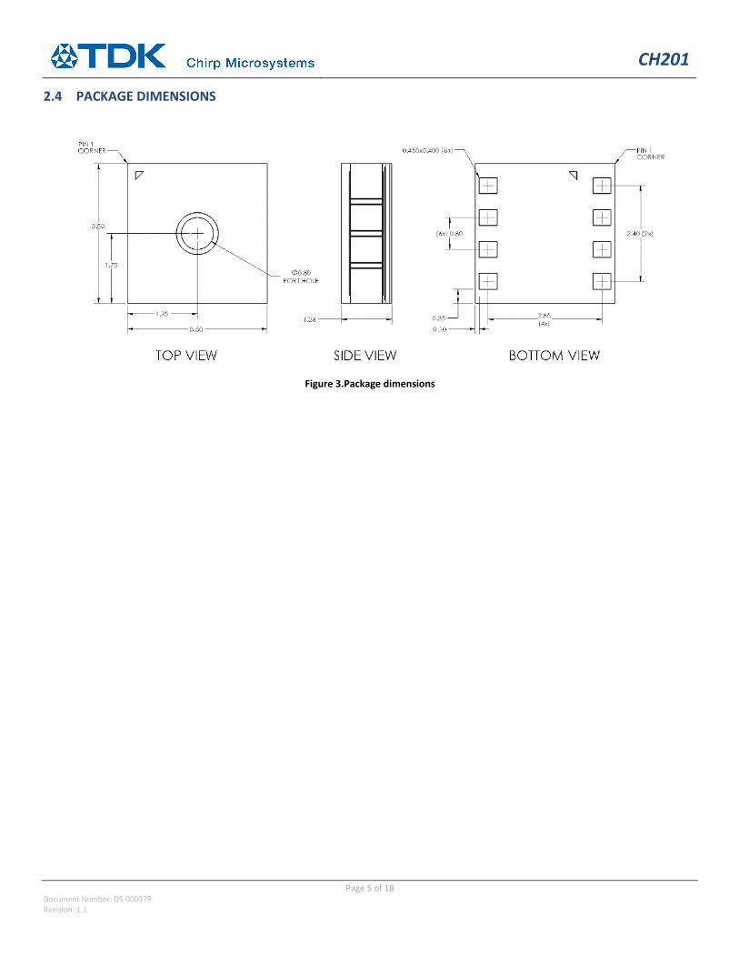
2.4 PACKAGE DIMENSIONS
Figure 3.Package dimensions

CH201
Page 6 of 18 Document Number: DS-000379 Revision: 1.1
3 ELECTRICAL CHARACTERISTICS AVDD = VDD = 1.8VDC, VSS = 0V, TA = +25°C, MIN/MAX ARE
FROM TA = -40°C TO +85°C, UNLESS OTHERWISE
SPECIFIED. PARAMETER
SYMBOL CONDITIONS MIN TYP MAX UNITS
POWER SUPPLY Analog Power Supply AVDD 1.62 1.8 1.98 V Digital Power Supply VDD 1.62 1.8 1.98 V
ULTRASONIC TRANSMIT CHANNEL Operating Frequency 85 kHz
TxRx OPERATION (GPR FIRMWARE LOADED)
Maximum Range Max Range Wall Target 58mm Diameter Post
5(1) 2.7(1)
m m
Minimum Range Min Range 0.2(2) m
Measuring Rate (Sample/sec) SR 5m 1m
25 100
Sample/s Sample/s
Field of View FoV Configurable up to 180º deg
Current Consumption (AVDD + VDD) IS
SR=1S/s, Range=1m SR=1S/s, Range=5m SR=25S/s, Range=1m SR=25S/s, Range=5m
8 14 63
247
μA μA μA μA
Measurement Time 5m max range 36 ms Programming Time 60 ms
Table 2.
Notes:
1. Measurement tested using 45° FoV acoustic housing. 2. Tested with a stationary target. While objects closer than 20 cm can be detected, the range measurement is not ensured.

CH201
Page 7 of 18 Document Number: DS-000379 Revision: 1.1
3.1 ELECTRICAL CHARACTERISTICS (CONT’D) AVDD = VDD = 1.8VDC, VSS = 0V, TA = +25°C, unless otherwise specified.
PARAMETER SYMBOL CONDITIONS MIN TYP MAX UNITS DIGITAL I/O CHARACTERISTICS
Output Low Voltage VOL SDA, INT, ISINK=XmA 0.4 V Output High Voltage VOH INT 0.9*VVDD V I2C Input Voltage Low VIL_I2C SDA, SCL 0.3*VVDD V I2C Input Voltage High VIH_I2C SDA, SCL 0.7*VVDD V Pin Leakage Current IL SDA,SCL, INT(Inactive),
TA=25°C ±1 μA
DIGITAL/I2C TIMING CHARACTERISTICS
SCL Clock Frequency fSCL I2C Fast Mode 400 kHz
Table 3. Electrical Characteristics Cont’d

CH201
Page 8 of 18 Document Number: DS-000379 Revision: 1.1
4 TYPICAL OPERATING CHARACTERISTICS AVDD = VDD = 1.8VDC, VSS = 0V, TA = +25°C, unless otherwise specified.
Figure 4. Typical Beam Pattern – MOD-CH201-00-01 45 deg FoV module
(Measured with a 1 m2 flat plate target at a 1m range)

CH201
Page 9 of 18 Document Number: DS-000379 Revision: 1.1
5 DETAILED DESCRIPTION 5.1 THEORY OF OPERATION The CH201 is an autonomous, digital output ultrasonic rangefinder. The Simplified Block Diagram in Figure 1 shows the main components at the package-level. The package includes a piezoelectric micro-machined ultrasonic transducer (PMUT) and system-on-chip (SoC). The SoC controls the PMUT to produce pulses of ultrasound that reflect off targets in the sensor’s Field of View (FoV). The reflections are received by the same PMUT after a short time delay, amplified by sensitive electronics, digitized, and further processed to produce the range to the primary target. Many algorithms can further process the range information for a variety of usage cases in a wide range of applications.
The time it takes the ultrasound pulse to propagate from the PMUT to the target and back is called the time-of-flight (ToF). The distance to the target is found by multiplying the time-of-flight by the speed of sound and dividing by two (to account for the round-trip). The speed of sound in air is approximately 343 m/s. The speed of sound is not a constant but is generally stable enough to give measurement accuracies within a few percent error.
5.2 DEVICE CONFIGURATION A CH201 program file must be loaded into the on-chip memory at initial power-on. The program, or firmware, is loaded through a special I2C interface. Chirp provides a default general-purpose rangefinder (GPR) firmware that is suitable for a wide range of applications. This firmware enables autonomous range finding operation of the CH201. It also supports hardware-triggering of the CH201 for applications requiring multiple transceivers. Program files can also be tailored to the customer’s application. Contact Chirp for more information.
CH201 has several features that allow for low power operation. An ultra-low-power, on-chip real-time clock (RTC) sets the sample rate and provides the reference for the time-of-flight measurement. The host processor does not need to provide any stimulus to the CH201 during normal operation, allowing the host processor to be shut down into its lowest power mode until the CH201 generates a wake-up interrupt. There is also a general-purpose input/output (INT) pin that is optimized to be used as a system wake-up source. The interrupt pin can be configured to trigger on motion or proximity.

CH201
Page 10 of 18 Document Number: DS-000379 Revision: 1.1
6 APPLICATIONS 6.1 CHIRP CH201 DRIVER Chirp provides a compiler- and microcontroller-independent C driver for the CH201 which greatly simplifies integration. The CH201 driver implements high-level control of one or more CH201s attached to one or more I2C ports on the host processor. The CH201 driver allows the user to program, configure, trigger, and readout data from the CH201 through use of C function calls without direct interaction with the CH201 I2C registers. The CH201 driver only requires the customer to implement an I/O layer which communicates with the host processor’s I2C hardware and GPIO hardware. Chirp highly recommends that all designs use the CH201 driver.
6.2 OBJECT DETECTION Detecting the presence of objects or people can be optimized via software, by setting the sensor’s full-scale range (FSR), and via hardware, using an acoustic housing to narrow or widen the sensor’s field-of-view. The former means that the user may set the maximum distance at which the sensor will detect an object. FSR values refer to the one-way distance to a detected object.
In practice, the FSR setting controls the amount of time that the sensor spends in the listening (receiving) period during a measurement cycle. Therefore, the FSR setting affects the time required to complete a measurement. Longer full-scale range values will require more time for a measurement to complete.
Ultrasonic signal processing using the CH201’s General Purpose Rangefinder (GPR) Firmware will detect echoes that bounce off the first target in the Field-of-View. The size, position, and material composition of the target will affect the maximum range at which the sensor can detect the target. Large targets, such as walls, are much easier to detect than smaller targets. Thus, the associated operating range for smaller targets will be shorter. The range to detect people will be affected by a variety of factors such as a person’s size, clothing, orientation to the sensor and the sensor’s field-of-view. In general, given these factors, people can be detected at a maximum distance of 3-4m away from the CH201 sensor.
For additional information, please refer to AN-000214 Presence Detection Application Note and associated Presence Detection S/W.
6.3 INTERFACING TO THE CH201 ULTRASONIC SENSOR The CH201 communicates with a host processor over the 2-wire I2C protocol. The CH201 operates as an I2C slave and responds to commands issued by the I2C master.
The CH201 contains two separate I2C interfaces, running on two separate slave addresses. The first is for loading firmware into the on-chip program memory, and the second is for in-application communication with the CH201. The 7-bit programming address is 0x45, and the 7-bit application address default is 0x29. The application address can be reprogrammed to any valid 7-bit I2C address.
The CH201 uses clock stretching to allow for enough time to respond to the I2C master. The CH201 clock stretches before the acknowledge (ACK) bit on both transmit and receive. For example, when the CH201 transmits, it will hold SCL low after it transmits the 8th bit from the current byte while it loads the next byte into its internal transmit buffer. When the next byte is ready, it releases the SCL line, reads the master’s ACK bit, and proceeds accordingly. When the CH201 is receiving, it holds the SCL line low after it receives the 8th bit in a byte. The CH201 then chooses whether to ACK or NACK depending on the received data and releases the SCL line.
Figure 5 shows an overview of the I2C slave interface. In the diagram, ‘S’ indicates I2C start, ‘R/W’ is the read/write bit, ‘Sr’ is a repeated start, ‘A’ is acknowledge, ‘P’ is the stop condition. Gray boxes indicate the I2C master actions; white boxes indicate the I2C slave actions.

CH201
Page 11 of 18 Document Number: DS-000379 Revision: 1.1
Figure 5. CH201 I2C Slave Interface Diagram
6.4 DEVICE MODES OF OPERATION
Free-Running Mode In the free-running measurement mode, the CH201 runs autonomously at a user specified sample rate. In this mode, the INT pin is configured as an output. The CH201 pulses the INT pin high when a new range sample is available. At this point, the host processor may read the sample data from the CH201 over the I2C interface.
Hardware-Triggered Mode In the hardware triggered mode, the INT pin is used bi-directionally. The CH201 remains in an idle condition until triggered by pulsing the INT pin. The measurement will start with deterministic latency relative to the rising edge on INT. This mode is most useful for synchronizing several CH201 transceivers. The host controller can use the individual INT pins of several transceivers to coordinate the exact timing.
CH201 Beam Patterns The acoustic Field of View is easily customizable for the CH201 and is achieved by adding an acoustic housing to the transceiver that is profiled to realize the desired beam pattern. Symmetric, asymmetric, and omnidirectional (180° FoV) beam patterns are realizable.
An example beam pattern is shown in the Typical Operating Characteristics section of this document and several acoustic housing designs for various FoV’s are available from Chirp.

CH201
Page 12 of 18 Document Number: DS-000379 Revision: 1.1
6.5 LAYOUT RECOMMENDATIONS
Recommended PCB Footprint
Dimensions in mm
Figure 6. Recommended PCB Footprint

CH201
Page 13 of 18 Document Number: DS-000379 Revision: 1.1
6.6 PCB REFLOW RECOMMENDATIONS: See App Note AN-000159 CH101 and CH201 Ultrasonic Transceiver Handling and Assembly Guidelines.
Use of Level Shifters While the use of autosense level shifters for all the digital I/O signal signals is acceptable, special handling of the INT line while using a level shifter is required to ensure proper resetting of this line. As the circuit stage is neither a push-pull nor open-drain configuration (see representative circuit in Figure 7 below), it is recommended that level shifter with a manual direction control line be used. The TI SN74LVC2T45 Bus Transceiver is a recommended device for level shifting of the INT signal line.
Figure 7. INT Line I/O Circuit Stage
6.7 TYPICAL OPERATING CIRCUITS
Figure 8. Single Transceiver Operation
SDA (Master)SCL (Master)GPIOGPIOGPIO
GND
VDDMicrocontroller
SDASCL
PROGINTRESET_N
VSS
VDD
AVDD23
145
6
78CH-201
0.1µF
SDASCL
PROGINTRESET_N
VSS
VDD
AVDD23
145
6
78
0.1µF
2k2
2k2
10k
1.8V
1.8V

CH201
Page 14 of 18 Document Number: DS-000379 Revision: 1.1
Figure 9. Multi-Transceiver Operation
SDA (Master)SCL (Master)GPIOGPIOGPIO
GND
VDDMicrocontroller
SDASCL
PROGINTRESET_N
VSS
VDD
AVDD23
145
6
78CH-201
0.1µF
SDASCL
PROGINTRESET_N
VSS
VDD
AVDD23
145
6
78CH-201
0.1µF
SDASCL
PROGINTRESET_N
VSS
VDD
AVDD23
145
6
78CH-201
0.1µF
SDASCL
PROGINTRESET_N
VSS
VDD
AVDD23
145
6
78
0.1µFGPIOGPIOGPIOGPIO
2k2
2k2
10k
1.8V
1.8V
1.8V
1.8V

CH201
Page 15 of 18 Document Number: DS-000379 Revision: 1.1
7 ORDERING INFORMATION 7.1 PART NUMBER DESIGNATION
Figure 10. Part Number Designation
This datasheet specifies the following part numbers
PART NUMBER PACKAGE BODY QUANTITY PACKAGING CH201-00ABR 3.5 mm x 3.5 mm x 1.26 mm LGA-8L 1,000 7” Tape and Reel
Table 4. CH201 Part Number
7.2 PACKAGE MARKING
Figure 11. Packaging Marking
CH201-xxABx Product Family
Product Variant Shipping Carrier R = Tape & Reel 00AB = Product Variant
CH201 = Long-Range Ultrasonic ToF Sensor

CH201
Page 16 of 18 Document Number: DS-000379 Revision: 1.1
7.3 TAPE & REEL SPECIFICATION
Figure 12. Tape & Reel Specifications
7.4 SHIPPING LABEL A Shipping Label will be attached to the reel, bag and box. The information provided on the label is as follows:
Device: This is the full part number
Lot Number: Chirp manufacturing lot number
Date Code: Date the lot was sealed in the moisture proof bag
Quantity: Number of components on the reel
2D Barcode: Contains Lot No., quantity and reel/bag/box number
Figure 13. Shipping Label
Dimensions in mm
CH201
Page 17 of 18 Document Number: DS-000379 Revision: 1.1
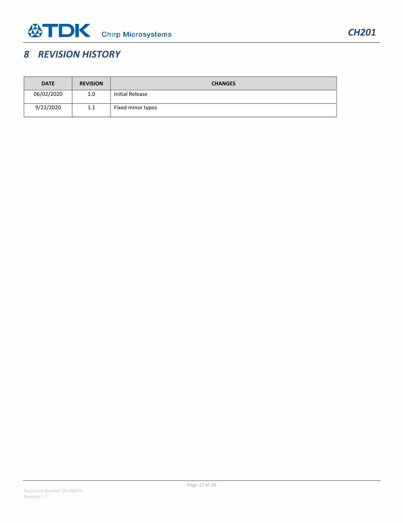
8 REVISION HISTORY
DATE REVISION CHANGES
06/02/2020 1.0 Initial Release
9/22/2020 1.1 Fixed minor typos

CH201
Page 18 of 18 Document Number: DS-000379 Revision: 1.1
This information furnished by Chirp Microsystems, Inc. (“Chirp Microsystems”) is believed to be accurate and reliable. However, no responsibility is assumed by Chirp Microsystems for its use, or for any infringements of patents or other rights of third parties that may result from its use. Specifications are subject to change without notice. Chirp Microsystems reserves the right to make changes to this product, including its circuits and software, in order to improve its design and/or performance, without prior notice. Chirp Microsystems makes no warranties, neither expressed nor implied, regarding the information and specifications contained in this document. Chirp Microsystems assumes no responsibility for any claims or damages arising from information contained in this document, or from the use of products and services detailed therein. This includes, but is not limited to, claims or damages based on the infringement of patents, copyrights, mask work and/or other intellectual property rights.
Certain intellectual property owned by Chirp Microsystems and described in this document is patent protected. No license is granted by implication or otherwise under any patent or patent rights of Chirp Microsystems. This publication supersedes and replaces all information previously supplied. Trademarks that are registered trademarks are the property of their respective companies. Chirp Microsystems sensors should not be used or sold in the development, storage, production or utilization of any conventional or mass-destructive weapons or for any other weapons or life threatening applications, as well as in any other life critical applications such as medical equipment, transportation, aerospace and nuclear instruments, undersea equipment, power plant equipment, disaster prevention and crime prevention equipment.
©2020 Chirp Microsystems. All rights reserved. Chirp Microsystems and the Chirp Microsystems logo are trademarks of Chirp Microsystems, Inc. The TDK logo is a trademark of TDK Corporation. Other company and product names may be trademarks of the respective companies with which they are associated.
©2020 Chirp Microsystems. All rights reserved.