ch06
DESCRIPTION
Design for testability lectureTRANSCRIPT

7/17/2019 ch06
http://slidepdf.com/reader/full/ch06563db960550346aa9a9cbebb 1/83
Chapter 6 VLSI Testing
Jin-Fu Li
Advanced Reliable Systems (ARES) Laboratory
Department of Electrical Engineering
National Central University
Jungli, Taiwan
7/17/2019 ch06
http://slidepdf.com/reader/full/ch06563db960550346aa9a9cbebb 2/83
Advanced Reliable Systems (ARES) Lab. Jin-Fu Li, EE, NCU 2
Basics
Fault Modeling
Design-for-Testability
Outline
7/17/2019 ch06
http://slidepdf.com/reader/full/ch06563db960550346aa9a9cbebb 3/83
Advanced Reliable Systems (ARES) Lab. Jin-Fu Li, EE, NCU 3
Basics
Fault Modeling
Design-for-Testability
Outline

7/17/2019 ch06
http://slidepdf.com/reader/full/ch06563db960550346aa9a9cbebb 4/83
Advanced Reliable Systems (ARES) Lab. Jin-Fu Li, EE, NCU 4
VLSI Realization Process
Determine requirements
Write specifications
Design synthesis and Verification
Fabrication
Manufacturing test
Chips to customer
Customer’s need
Test development
7/17/2019 ch06
http://slidepdf.com/reader/full/ch06563db960550346aa9a9cbebb 5/83
Advanced Reliable Systems (ARES) Lab. Jin-Fu Li, EE, NCU 5
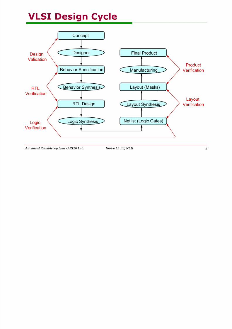
VLSI Design Cycle
Concept
Behavior Specification
Designer
Behavior Synthesis
RTL Design
Logic Synthesis Netlist (Logic Gates)
Layout Synthesis
Layout (Masks)
Manufacturing
Final ProductDesign
Validation
RTL
Verification
Layout
Verification
Logic
Verification
Product
Verification
7/17/2019 ch06
http://slidepdf.com/reader/full/ch06563db960550346aa9a9cbebb 6/83
Advanced Reliable Systems (ARES) Lab. Jin-Fu Li, EE, NCU 6
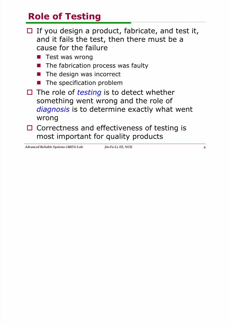
Role of Testing
If you design a product, fabricate, and test it,and it fails the test, then there must be acause for the failure
Test was wrong The fabrication process was faulty
The design was incorrect
The specification problem
The role of testing is to detect whethersomething went wrong and the role ofdiagnosis is to determine exactly what wentwrong
Correctness and effectiveness of testing ismost important for quality products
7/17/2019 ch06
http://slidepdf.com/reader/full/ch06563db960550346aa9a9cbebb 7/83
Advanced Reliable Systems (ARES) Lab. Jin-Fu Li, EE, NCU 7
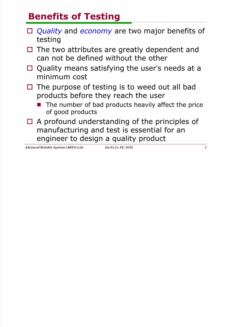
Benefits of Testing
Quality and economy are two major benefits oftesting
The two attributes are greatly dependent and
can not be defined without the other Quality means satisfying the user’s needs at a
minimum cost
The purpose of testing is to weed out all badproducts before they reach the user
The number of bad products heavily affect the price
of good products A profound understanding of the principles of
manufacturing and test is essential for anengineer to design a quality product

7/17/2019 ch06
http://slidepdf.com/reader/full/ch06563db960550346aa9a9cbebb 8/83
Advanced Reliable Systems (ARES) Lab. Jin-Fu Li, EE, NCU 8
Trends of Testing
Two key factors are changing the way of VLSIICs testing
The manufacturing test cost has been not scaling
The effort to generate tests has been growinggeometrically along with product complexity
1
0.1
0.01
0.001
0.0001
0.00001
0.000001
0.0000001
Cost: cents/transistor
1982 1985 1988 1991 1994 1997 2000 2003 2006 2009 2012
Si capital/transistor
Test capital/transistor
Source: SIA
7/17/2019 ch06
http://slidepdf.com/reader/full/ch06563db960550346aa9a9cbebb 9/83
Advanced Reliable Systems (ARES) Lab. Jin-Fu Li, EE, NCU 9
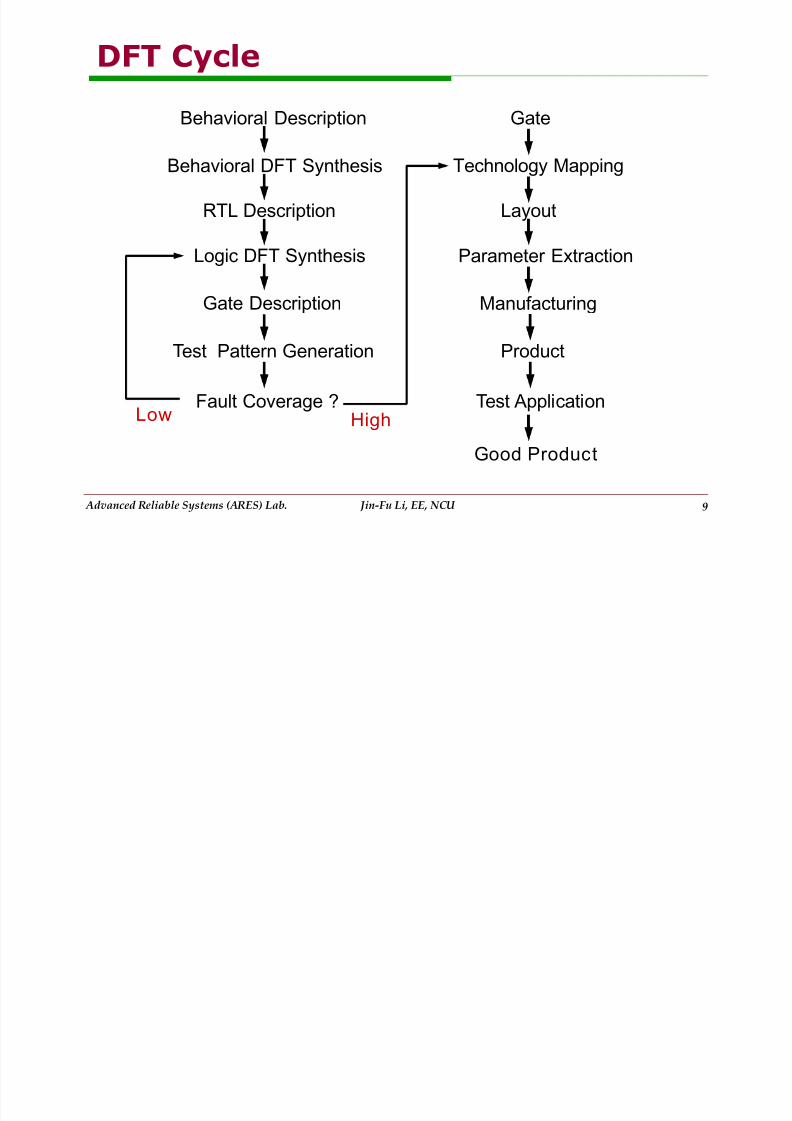
DFT Cycle
Behavioral Description
Behavioral DFT Synthesis
RTL Description
Logic DFT Synthesis
Gate Description
Test Pattern Generation
Fault Coverage ?
Gate
Technology Mapping
Layout
Parameter Extraction
Test Application
Good Product
Manufacturing
Product
HighLow
7/17/2019 ch06
http://slidepdf.com/reader/full/ch06563db960550346aa9a9cbebb 10/83
Advanced Reliable Systems (ARES) Lab. Jin-Fu Li, EE, NCU 10
As Technology Scales Continuously
Die size, chip yield, and design productivityhave so far limited transistor integration in aVLSI design
Now the focus has shifted to energyconsumption, power dissipation, and powerdelivery
As technology scales further we will face newchallenges, such as variability, single-eventupsets (soft errors), and device (transistor
performance) degradation−
these effectsmanifesting as inherent u n r e l i a b i l i t y of thecomponents, posing design and test challenges
Source: S. Borkar (Intel Corp.), IEEE Micro, 2005
7/17/2019 ch06
http://slidepdf.com/reader/full/ch06563db960550346aa9a9cbebb 11/83
Advanced Reliable Systems (ARES) Lab. Jin-Fu Li, EE, NCU 11
Possible Solution to Conquer Unreliability
The key to the reliability problem might be to exploitthe abundance of transistors−use Moore’s low to
advantage. Instead of relying on higher and higher
frequency of operation to deliver higher performance, a shift toward parallelism to deliver higher performance
is in order, and thus multi might be the solution at all
levels− from multiplicity of functional blocks to multiple
processor cores in a system
Source: S. Borkar (Intel Corp.), IEEE Micro, 2005
7/17/2019 ch06
http://slidepdf.com/reader/full/ch06563db960550346aa9a9cbebb 12/83
Advanced Reliable Systems (ARES) Lab. Jin-Fu Li, EE, NCU 12
Possible Solution to Conquer Unreliability
We could distribute test functionality as a part of thehardware to dynamically detect errors, or to correct and
isolate aging and faulty hardware. Or a subset of cores
in the multicore design could perform this work. Thismicroarchitecture strategy, with multicores to assist in
redundancy, is called resilient microarchitecture. It
continuously detects errors, isolates faults, confines faults, reconfigures the hardware, and thus adapts. If we
can make such a strategy work, there is no need for on-
time factory testing, burn in, since the system is capableof testing and reconfiguring itself to make itself work
reliably throughout its lifetime.
Source: S. Borkar (Intel Corp.), IEEE Micro, 2005

7/17/2019 ch06
http://slidepdf.com/reader/full/ch06563db960550346aa9a9cbebb 13/83
Advanced Reliable Systems (ARES) Lab. Jin-Fu Li, EE, NCU 13
Itanium (JSSC, Jan. 2006)
7/17/2019 ch06
http://slidepdf.com/reader/full/ch06563db960550346aa9a9cbebb 14/83
Advanced Reliable Systems (ARES) Lab. Jin-Fu Li, EE, NCU 14
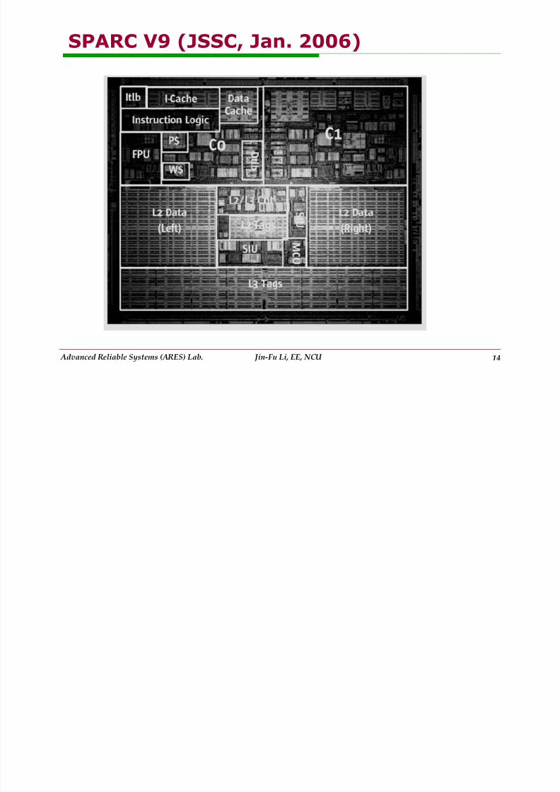
SPARC V9 (JSSC, Jan. 2006)

7/17/2019 ch06
http://slidepdf.com/reader/full/ch06563db960550346aa9a9cbebb 15/83
Advanced Reliable Systems (ARES) Lab. Jin-Fu Li, EE, NCU 15
Cell Processor (JSSC, Jan. 2006)

7/17/2019 ch06
http://slidepdf.com/reader/full/ch06563db960550346aa9a9cbebb 16/83
Advanced Reliable Systems (ARES) Lab. Jin-Fu Li, EE, NCU 16
Verification & Test
Verification
Verifies correctness of design
Performed by simulation, hardware emulation, or
formal methods
Perform once before manufacturing
Responsible for quality of design
Test
Verifies correctness of manufactured hardware
Two-part process Test generation: software process executed
once during design
Test application: electrical tests applied to
hardware Test application performed on every manufactured
device
Responsible for quality of device

7/17/2019 ch06
http://slidepdf.com/reader/full/ch06563db960550346aa9a9cbebb 17/83
Advanced Reliable Systems (ARES) Lab. Jin-Fu Li, EE, NCU 17
Verification & Test
Specification
Netlist
Silicon
Verification
Test
Hardware design
Manufacturing
Reconvergent path model
7/17/2019 ch06
http://slidepdf.com/reader/full/ch06563db960550346aa9a9cbebb 18/83
Advanced Reliable Systems (ARES) Lab. Jin-Fu Li, EE, NCU 18
Defect, Fault, and Error
Defect A defect is the unintended difference between the
implemented hardware and its intended design
Defects occur either during manufacture or duringthe use of devices
Fault
A representation of a defect at the abstractedfunction level
Error
A wrong output signal produced by a defective
system An error is caused by a Fault or a design error

7/17/2019 ch06
http://slidepdf.com/reader/full/ch06563db960550346aa9a9cbebb 19/83
Advanced Reliable Systems (ARES) Lab. Jin-Fu Li, EE, NCU 19
Typical Types of Defects
Extra and missing material Primarily caused by dust particles on the mask or
wafer surface, or in the processing chemicals
Oxide breakdown Primarily caused by insufficient oxygen at the
interface of silicon (Si) and silicon dioxide (SiO2),chemical contamination, and crystal defects
Electromigration
Primarily caused by the transport of metal atomswhen a current flows through the wire
Because of a low melting point, aluminum has largeself-diffusion properties, which increase itselectromigration liability

7/17/2019 ch06
http://slidepdf.com/reader/full/ch06563db960550346aa9a9cbebb 20/83
Advanced Reliable Systems (ARES) Lab. Jin-Fu Li, EE, NCU 20
Example
Consider one two-input AND gate
Defect: a short to ground
Fault: signal b stuck at logic 0
Error: a=1, b=1, c=0 (correct output c=1)
Note that the error is not permanent. As longas at least one input is 0, there is no error in
the output
ab
c
ab
cab
Gnd

7/17/2019 ch06
http://slidepdf.com/reader/full/ch06563db960550346aa9a9cbebb 21/83
Advanced Reliable Systems (ARES) Lab. Jin-Fu Li, EE, NCU 21
Defect, Fault, and Error
Different types of defects may cause the samefault
Different types of faults may cause the same
error E.g., A stuck-at-0, Y=1; C stuck-at-1, Y=1
bca
bca
CD
AB Y
S/0
S/1
7/17/2019 ch06
http://slidepdf.com/reader/full/ch06563db960550346aa9a9cbebb 22/83
Advanced Reliable Systems (ARES) Lab. Jin-Fu Li, EE, NCU 22
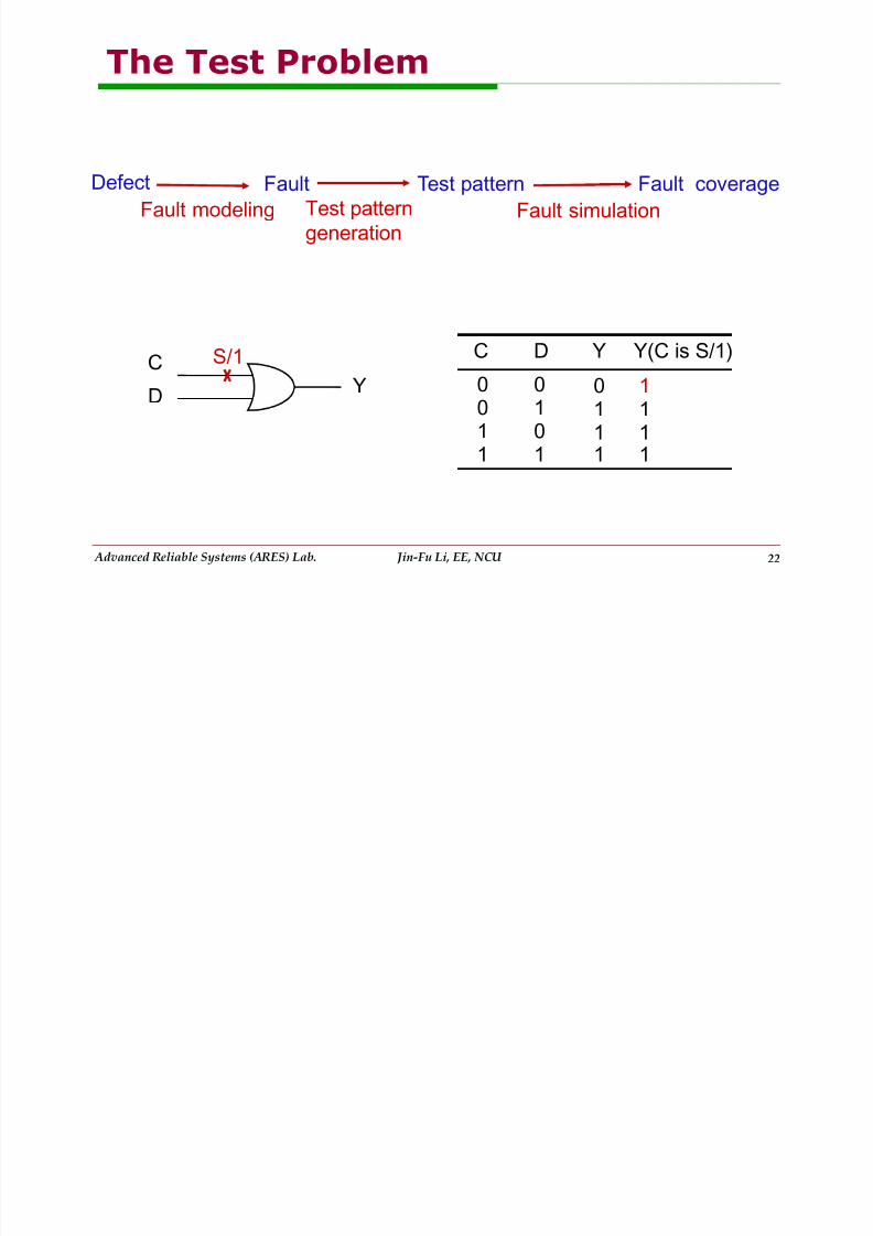
The Test Problem
Defect Fault Test pattern Fault coverage
Fault modelingTest pattern
generation Fault simulation
C
D
S/1
Y
C D
0 00 1
1 01 1
Y Y(C is S/1)
0 11 1
1 11 1
7/17/2019 ch06
http://slidepdf.com/reader/full/ch06563db960550346aa9a9cbebb 23/83
Advanced Reliable Systems (ARES) Lab. Jin-Fu Li, EE, NCU 23
Ideal Tests & Real Tests
The problems of ideal tests Ideal tests detect all defects produced in the
manufacturing process
Ideal tests pass all functionally good devices
Very large numbers and varieties of possible defectsneed to be tested
Difficult to generate tests for some real defects
Real tests Based on analyzable fault models, which may not map on
real defects
Incomplete coverage of modeled faults due to highcomplexity
Some good chips are rejected. The fraction (orpercentage) of such chips is called the yield loss
Some bad chips pass tests. The fraction (or percentage)of bad chips among all passing chips is called the defectlevel
7/17/2019 ch06
http://slidepdf.com/reader/full/ch06563db960550346aa9a9cbebb 24/83
Advanced Reliable Systems (ARES) Lab. Jin-Fu Li, EE, NCU 24
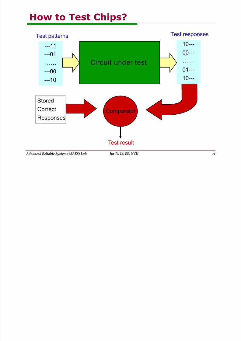
How to Test Chips?
Circuit under test
---11
---01
……
---00
---10
10---
00---
……01---
10---
Stored
Correct
Responses
Comparator
Test result
Test patterns Test responses

7/17/2019 ch06
http://slidepdf.com/reader/full/ch06563db960550346aa9a9cbebb 25/83
Advanced Reliable Systems (ARES) Lab. Jin-Fu Li, EE, NCU 25
Cost of Test
Design for testability (DFT) Chip area overhead and yield reduction
Performance overhead
Software processes of test Test generation and fault simulation
Test programming and debugging
Manufacturing test Automatic test equipment (ATE) capital cost
Test center operational cost

7/17/2019 ch06
http://slidepdf.com/reader/full/ch06563db960550346aa9a9cbebb 26/83
Advanced Reliable Systems (ARES) Lab. Jin-Fu Li, EE, NCU 26
ADVENTEST Model T6682 ATE
Consists of
Powerful computer
Powerful 32-bit digital
signal processor (DSP)for analog testing
Probe head: actually
touches the bare diesor packaged chips toperform fault detectionexperiments
Probe card: containselectronics to measurechip pin or pad
7/17/2019 ch06
http://slidepdf.com/reader/full/ch06563db960550346aa9a9cbebb 27/83
Advanced Reliable Systems (ARES) Lab. Jin-Fu Li, EE, NCU 27
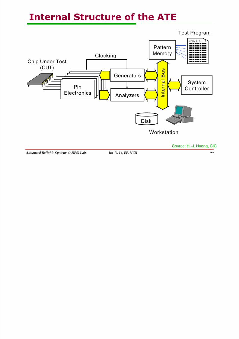
Internal Structure of the ATE
Chip Under Test(CUT)
Pin
ElectronicsPin
ElectronicsPin
ElectronicsPin
Electronics
Pin
Electronics
Pin
ElectronicsPin
Electronics
STIL 1.0;
Test Program
Pattern
Memory
I n t e
r n a l B u s
Workstation
Disk
Generators
Analyzers
Clocking
System
Controller
Source: H.-J. Huang, CIC
7/17/2019 ch06
http://slidepdf.com/reader/full/ch06563db960550346aa9a9cbebb 28/83
Advanced Reliable Systems (ARES) Lab. Jin-Fu Li, EE, NCU 28
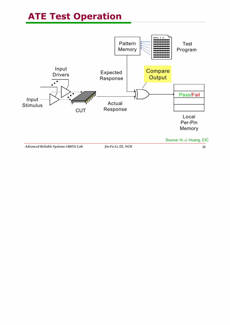
ATE Test Operation
Source: H.-J. Huang, CIC
Expected
Response
Actual
Response
Compare
Output
Compare
Output
STIL 1.0;
Test
Program
Pattern
Memory
CUT
Input
Stimulus
Input
Drivers
Pass/Fail
LocalPer-Pin
Memory
7/17/2019 ch06
http://slidepdf.com/reader/full/ch06563db960550346aa9a9cbebb 29/83
Advanced Reliable Systems (ARES) Lab. Jin-Fu Li, EE, NCU 29
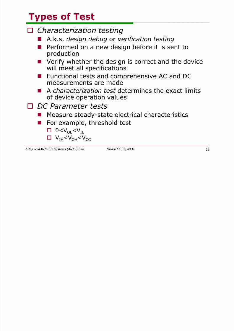
Types of Test
Characterization testing A.k.s. design debug or verification testing
Performed on a new design before it is sent toproduction
Verify whether the design is correct and the devicewill meet all specifications
Functional tests and comprehensive AC and DCmeasurements are made
A characterization test determines the exact limitsof device operation values
DC Parameter tests
Measure steady-state electrical characteristics For example, threshold test
0<VOL<VIL
VIH<VOH<VCC

7/17/2019 ch06
http://slidepdf.com/reader/full/ch06563db960550346aa9a9cbebb 30/83
Advanced Reliable Systems (ARES) Lab. Jin-Fu Li, EE, NCU 30
Types of Test
AC parametric tests Measure transient electronic characteristics
For example:
Rise time & fall time tests
7/17/2019 ch06
http://slidepdf.com/reader/full/ch06563db960550346aa9a9cbebb 31/83
Advanced Reliable Systems (ARES) Lab. Jin-Fu Li, EE, NCU 31
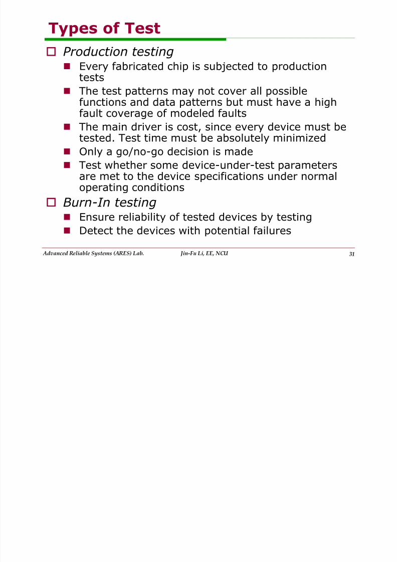
Types of Test
Production testing Every fabricated chip is subjected to production
tests
The test patterns may not cover all possible
functions and data patterns but must have a highfault coverage of modeled faults
The main driver is cost, since every device must betested. Test time must be absolutely minimized
Only a go/no-go decision is made Test whether some device-under-test parameters
are met to the device specifications under normaloperating conditions
Burn-In testing Ensure reliability of tested devices by testing
Detect the devices with potential failures

7/17/2019 ch06
http://slidepdf.com/reader/full/ch06563db960550346aa9a9cbebb 32/83
Advanced Reliable Systems (ARES) Lab. Jin-Fu Li, EE, NCU 32
Types of Test
The potential failures can be accelerated at elevatedtemperatures
The devices with infant mortality failures may bescreened out by a short-term burn-in test in anaccelerate
Failure rate versus product lifetime (bathtubcurve)
Time
F ai l ur
er a t e
Infant
mortality
Working lifetime Wear out
7/17/2019 ch06
http://slidepdf.com/reader/full/ch06563db960550346aa9a9cbebb 33/83
Advanced Reliable Systems (ARES) Lab. Jin-Fu Li, EE, NCU 33
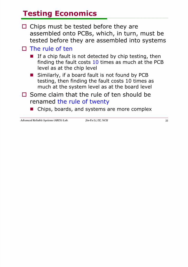
Testing Economics
Chips must be tested before they areassembled onto PCBs, which, in turn, must betested before they are assembled into systems
The rule of ten If a chip fault is not detected by chip testing, then
finding the fault costs 10 times as much at the PCBlevel as at the chip level
Similarly, if a board fault is not found by PCBtesting, then finding the fault costs 10 times asmuch at the system level as at the board level
Some claim that the rule of ten should berenamed the rule of twenty
Chips, boards, and systems are more complex
S Chi i ld
7/17/2019 ch06
http://slidepdf.com/reader/full/ch06563db960550346aa9a9cbebb 34/83
Advanced Reliable Systems (ARES) Lab. Jin-Fu Li, EE, NCU 34
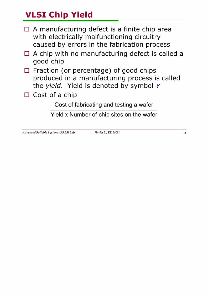
VLSI Chip Yield
A manufacturing defect is a finite chip areawith electrically malfunctioning circuitrycaused by errors in the fabrication process
A chip with no manufacturing defect is called agood chip
Fraction (or percentage) of good chips
produced in a manufacturing process is calledthe yield . Yield is denoted by symbol Y
Cost of a chip
Cost of fabricating and testing a wafer
Yield x Number of chip sites on the wafer
VLSI Chi Yi ld
7/17/2019 ch06
http://slidepdf.com/reader/full/ch06563db960550346aa9a9cbebb 35/83
Advanced Reliable Systems (ARES) Lab. Jin-Fu Li, EE, NCU 35
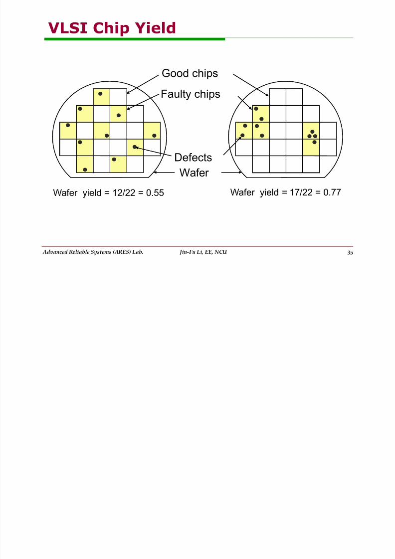
VLSI Chip Yield
Wafer
Defects
Faulty chips
Good chips
Wafer yield = 12/22 = 0.55 Wafer yield = 17/22 = 0.77
F lt C & D f t L l

7/17/2019 ch06
http://slidepdf.com/reader/full/ch06563db960550346aa9a9cbebb 36/83
Advanced Reliable Systems (ARES) Lab. Jin-Fu Li, EE, NCU 36
Fault Coverage & Defect Level
Fault coverage (FC) The measure of the ability of a test (a collection of
test patterns) to detect a given faults that mayoccur on the device under test
FC=#(detected faults)/#(possible faults)
Defect level (DL) The ratio of faulty chips among the chips that pass
tests DL is measured as defects per million (DPM)
DL is a measure of the effectiveness of tests
DL is a quantitative measure of the manufactured
product quality. For commercial VLSI chips a DLgreater than 500 DPM is considered unacceptable
and)1(1 FC Y DL
Y DL 10
D f t L l & Q lit L l
7/17/2019 ch06
http://slidepdf.com/reader/full/ch06563db960550346aa9a9cbebb 37/83
Advanced Reliable Systems (ARES) Lab. Jin-Fu Li, EE, NCU 37
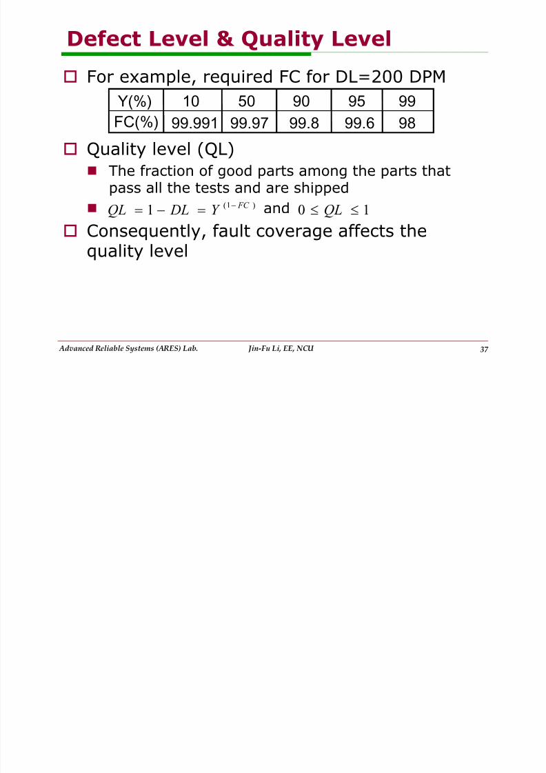
Defect Level & Quality Level
For example, required FC for DL=200 DPM
Quality level (QL)
The fraction of good parts among the parts thatpass all the tests and are shipped
and
Consequently, fault coverage affects thequality level
)1(1 FC Y DLQL 10 QL
Y(%)
FC(%)
10
99.991
50
99.97
90
99.8
95
99.6
99
98
Outline
7/17/2019 ch06
http://slidepdf.com/reader/full/ch06563db960550346aa9a9cbebb 38/83
Advanced Reliable Systems (ARES) Lab. Jin-Fu Li, EE, NCU 38
Basics
Fault Modeling
Design-for-Testability
Outline
Test Process
7/17/2019 ch06
http://slidepdf.com/reader/full/ch06563db960550346aa9a9cbebb 39/83
Advanced Reliable Systems (ARES) Lab. Jin-Fu Li, EE, NCU 39
Test Process
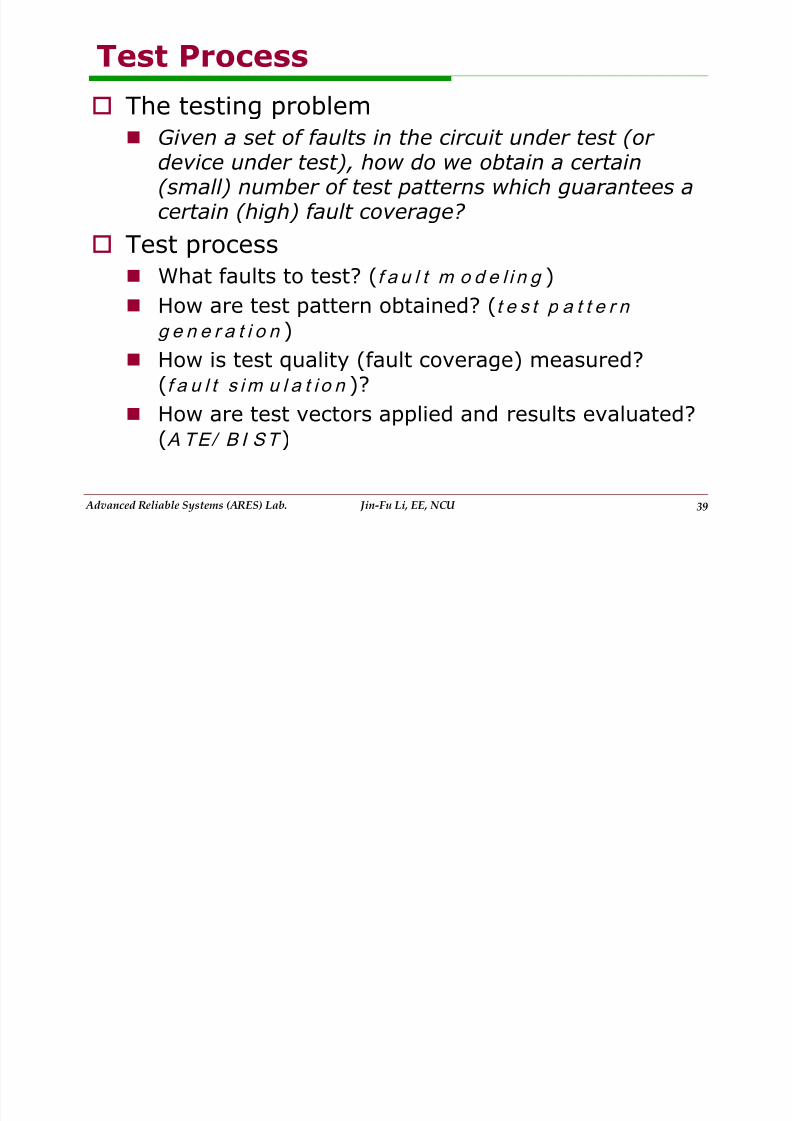
The testing problem Given a set of faults in the circuit under test (or
device under test), how do we obtain a certain(small) number of test patterns which guarantees a
certain (high) fault coverage?
Test process
What faults to test? (f a u l t m o d e l i n g )
How are test pattern obtained? (t e s t p a t t e r ng e n e r a t i o n )
How is test quality (fault coverage) measured?(f a u l t s im u l a t i o n )?
How are test vectors applied and results evaluated?(A TE/ B I ST )
Defect Categories

7/17/2019 ch06
http://slidepdf.com/reader/full/ch06563db960550346aa9a9cbebb 40/83
Advanced Reliable Systems (ARES) Lab. Jin-Fu Li, EE, NCU 40
Defect Categories
Defect categories Random defects, which are independent of designs
and processes
Systematic defects, which depend on designs andprocesses used for manufacturing
For example, random defects might be caused byrandom particles scattered on a wafer during
manufacturing
A resistive open defect [Source: Cadence]
Logical Fault Models

7/17/2019 ch06
http://slidepdf.com/reader/full/ch06563db960550346aa9a9cbebb 41/83
Advanced Reliable Systems (ARES) Lab. Jin-Fu Li, EE, NCU 41
Logical Fault Models
Systematic defects might be caused by processvariations, signal integrity, and design integrityissues.
It is possible both random and systematic defectscould happen on a single die
With the continuous shrinking of feature sizes,somewhere below the 180nm technology node,
system defects have a larger impact on yield thanrandom defects
Logical faults
Logical faults represent the physical defects on thebehaviors of the systems
Why Model Faults
7/17/2019 ch06
http://slidepdf.com/reader/full/ch06563db960550346aa9a9cbebb 42/83
Advanced Reliable Systems (ARES) Lab. Jin-Fu Li, EE, NCU 42
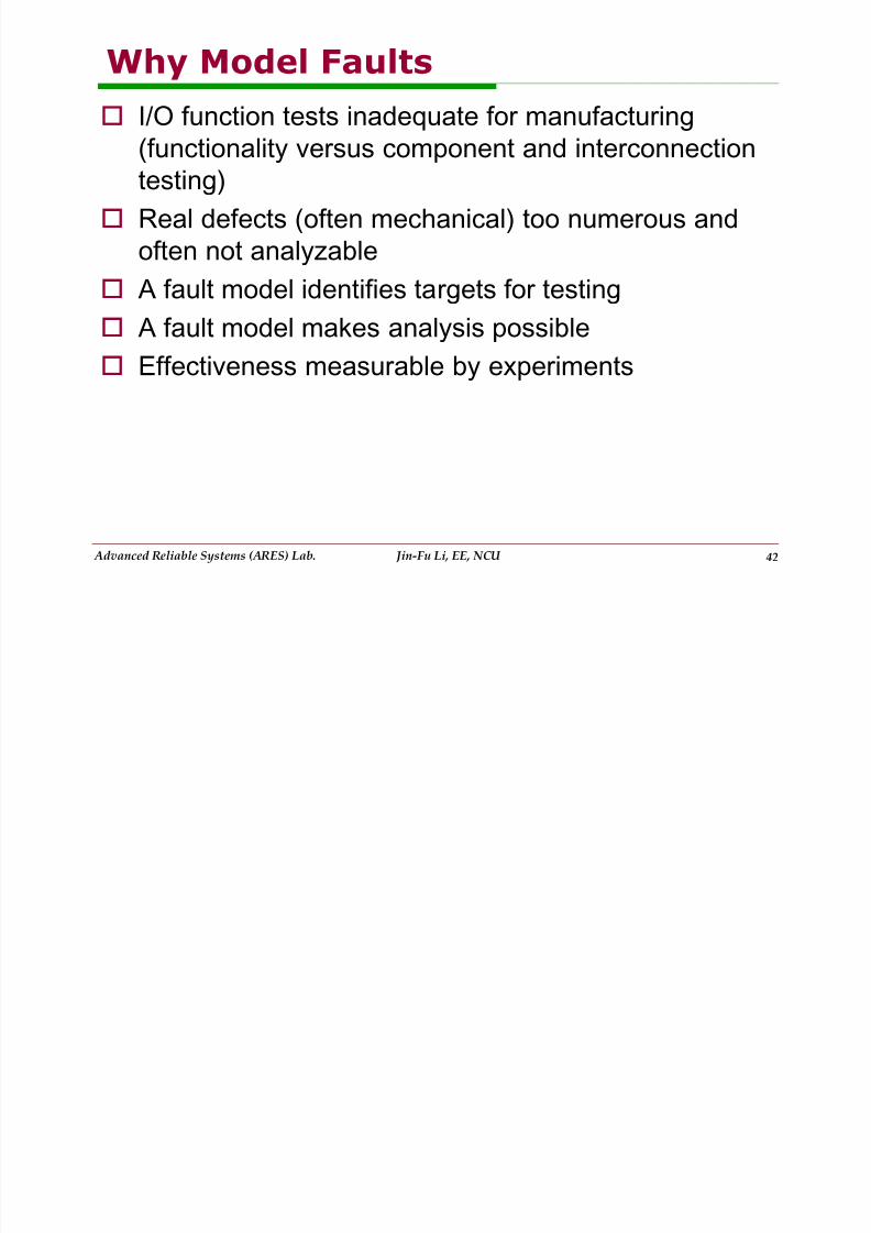
Why Model Faults
I/O function tests inadequate for manufacturing(functionality versus component and interconnection
testing)
Real defects (often mechanical) too numerous andoften not analyzable
A fault model identifies targets for testing
A fault model makes analysis possible Effectiveness measurable by experiments
Single Stuck-At Fault

7/17/2019 ch06
http://slidepdf.com/reader/full/ch06563db960550346aa9a9cbebb 43/83
Advanced Reliable Systems (ARES) Lab. Jin-Fu Li, EE, NCU 43
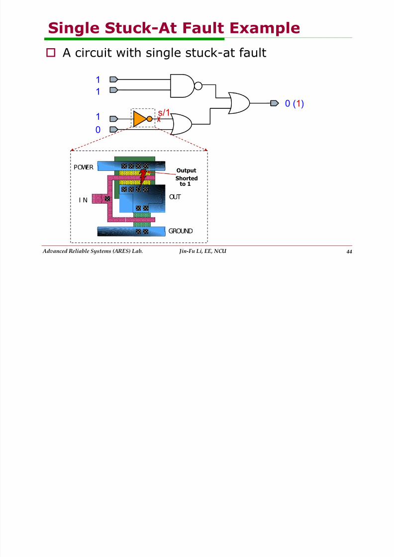
Single Stuck-At Fault
Single (line) stuck-at fault The given line has a constant value (0/1)
independent of other signal values in the circuit
Properties Only one line is faulty
The faulty line is permanently set to 0 or 1
The fault can be at an input or output of a gate
Simple logical model is independent of technologydetails
It reduces the complexity of fault-detection
algorithms One stuck-at fault can model more than one
kind of defect
Single Stuck-At Fault Example
7/17/2019 ch06
http://slidepdf.com/reader/full/ch06563db960550346aa9a9cbebb 44/83
Advanced Reliable Systems (ARES) Lab. Jin-Fu Li, EE, NCU 44
A circuit with single stuck-at fault
Single Stuck-At Fault Example
Output
Shortedto 1
I N OUT
GROUND
POWER
s/1
1
1
1
0
0 (1)
Number of Single Stuck-At Faults
7/17/2019 ch06
http://slidepdf.com/reader/full/ch06563db960550346aa9a9cbebb 45/83
Advanced Reliable Systems (ARES) Lab. Jin-Fu Li, EE, NCU 45
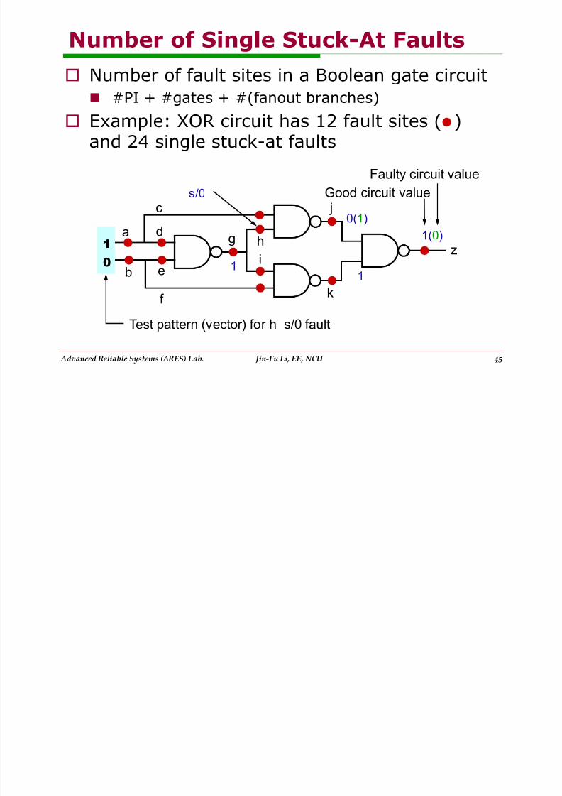
Number of Single Stuck At Faults
Number of fault sites in a Boolean gate circuit #PI + #gates + #(fanout branches)
Example: XOR circuit has 12 fault sites ( )
and 24 single stuck-at faults
a
b
c
d
e
f
1
0
g h
i1
s/0
j
k
z
0(1)
1(0)
1
Test pattern (vector) for h s/0 fault
Good circuit value
Faulty circuit value
Transistor Faults

7/17/2019 ch06
http://slidepdf.com/reader/full/ch06563db960550346aa9a9cbebb 46/83
Advanced Reliable Systems (ARES) Lab. Jin-Fu Li, EE, NCU 46
Transistor Faults
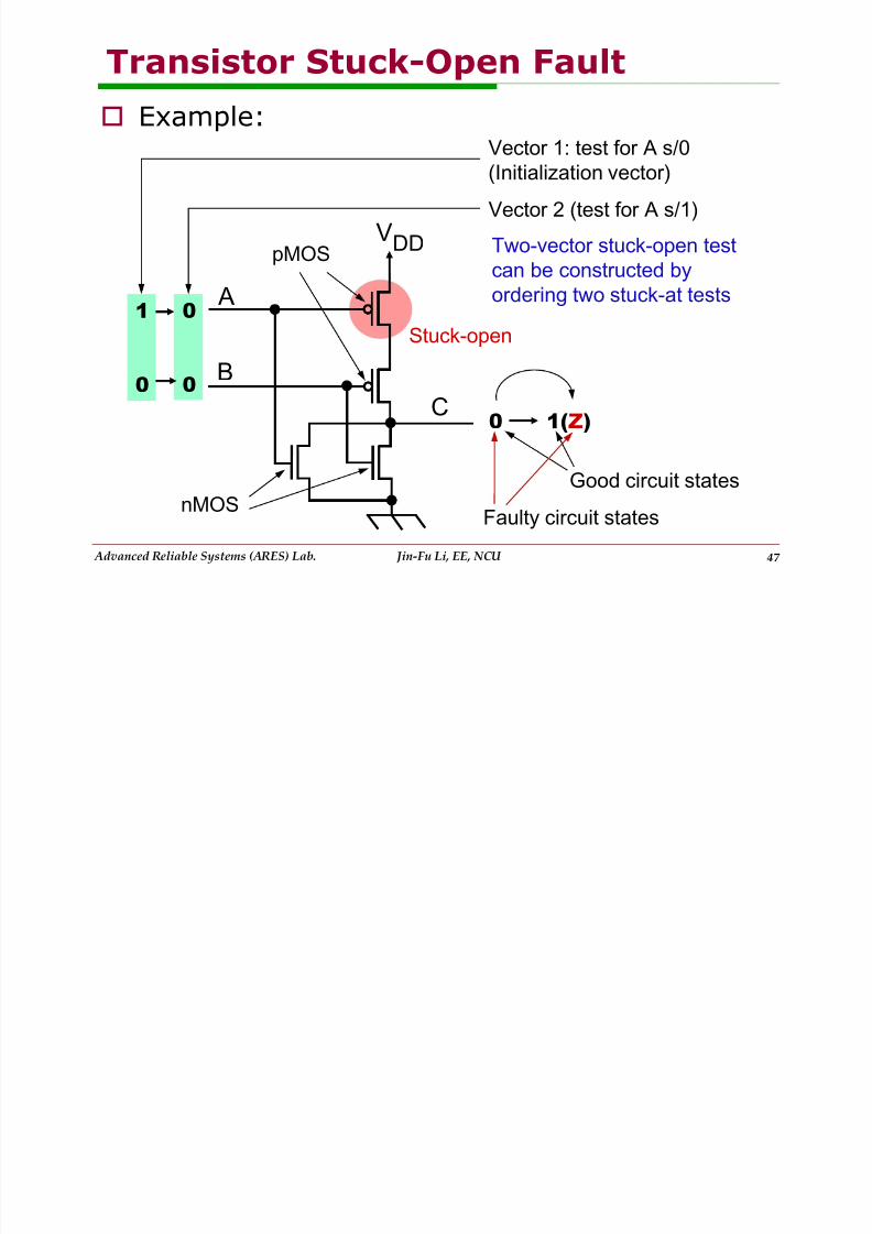
MOS transistor is considered an ideal switchand two types of faults are modeled
S t u c k - o p e n -- a single transistor is permanentlystuck in the open state
Turn the circuit into a sequential one
Need a sequence of at least 2 tests to detect a singlefault
Unique to CMOS circuits
S t u c k - o n -- a single transistor is permanentlyshorted irrespective of its gate voltage
Detection of a stuck-open fault requires two
vectors
Detection of a stuck-short fault requires themeasurement of quiescent current (IDDQ)
Transistor Stuck-Open Fault
7/17/2019 ch06
http://slidepdf.com/reader/full/ch06563db960550346aa9a9cbebb 47/83
Advanced Reliable Systems (ARES) Lab. Jin-Fu Li, EE, NCU 47
Transistor Stuck Open Fault
Example:
Two-vector stuck-open test
can be constructed by
ordering two stuck-at tests A
B
VDD
C
pMOS
nMOS
Stuck-open
1
0
0
0
0 1(Z)
Good circuit states
Faulty circuit states
Vector 1: test for A s/0
(Initialization vector)
Vector 2 (test for A s/1)
Test Stuck-On Fault Using IDDQ
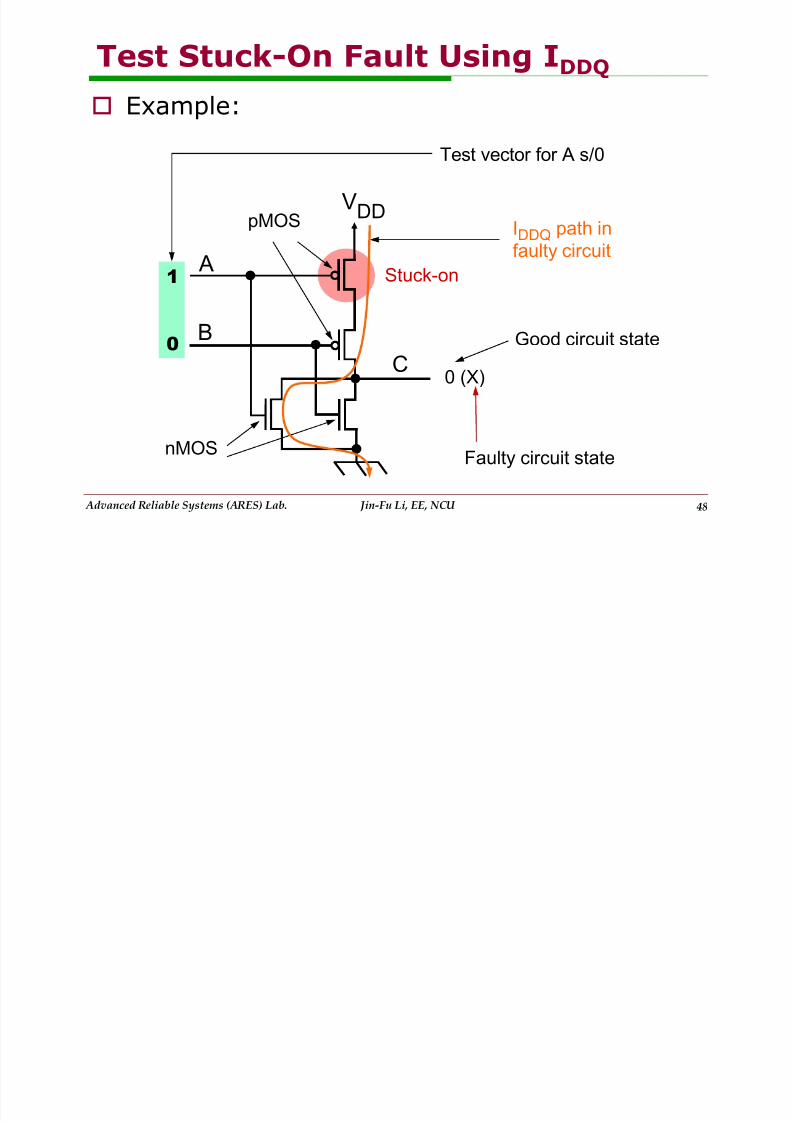
7/17/2019 ch06
http://slidepdf.com/reader/full/ch06563db960550346aa9a9cbebb 48/83
Advanced Reliable Systems (ARES) Lab. Jin-Fu Li, EE, NCU 48
Test Stuck On Fault Using IDDQ
Example:
A
B
VDD
C
pMOS
nMOS
Stuck-on1
0
0 (X)
Good circuit state
Faulty circuit state
Test vector for A s/0
IDDQ path in
faulty circuit
IDDQ Test in Nano-scale Era
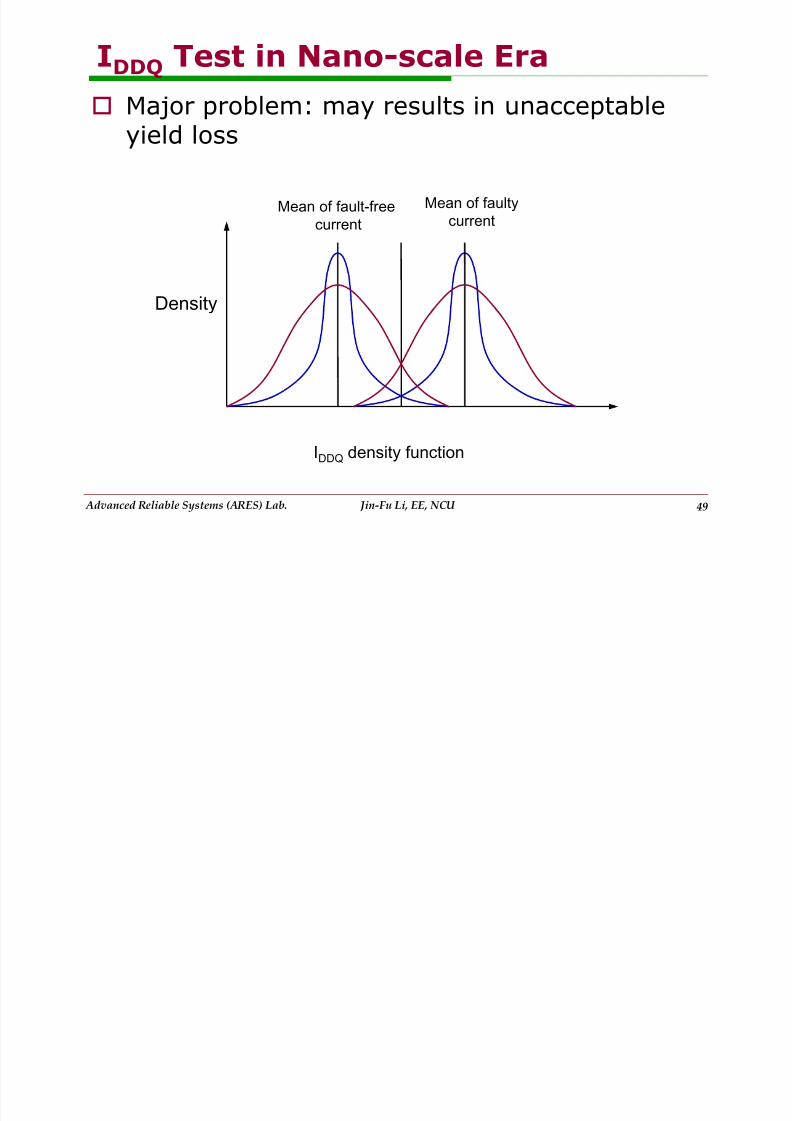
7/17/2019 ch06
http://slidepdf.com/reader/full/ch06563db960550346aa9a9cbebb 49/83
Advanced Reliable Systems (ARES) Lab. Jin-Fu Li, EE, NCU 49
IDDQ Test in Nano scale Era
Major problem: may results in unacceptableyield loss
IDDQ density function
Density
Mean of fault-freecurrent
Mean of faultycurrent
Test & Test Set
7/17/2019 ch06
http://slidepdf.com/reader/full/ch06563db960550346aa9a9cbebb 50/83
Advanced Reliable Systems (ARES) Lab. Jin-Fu Li, EE, NCU 50
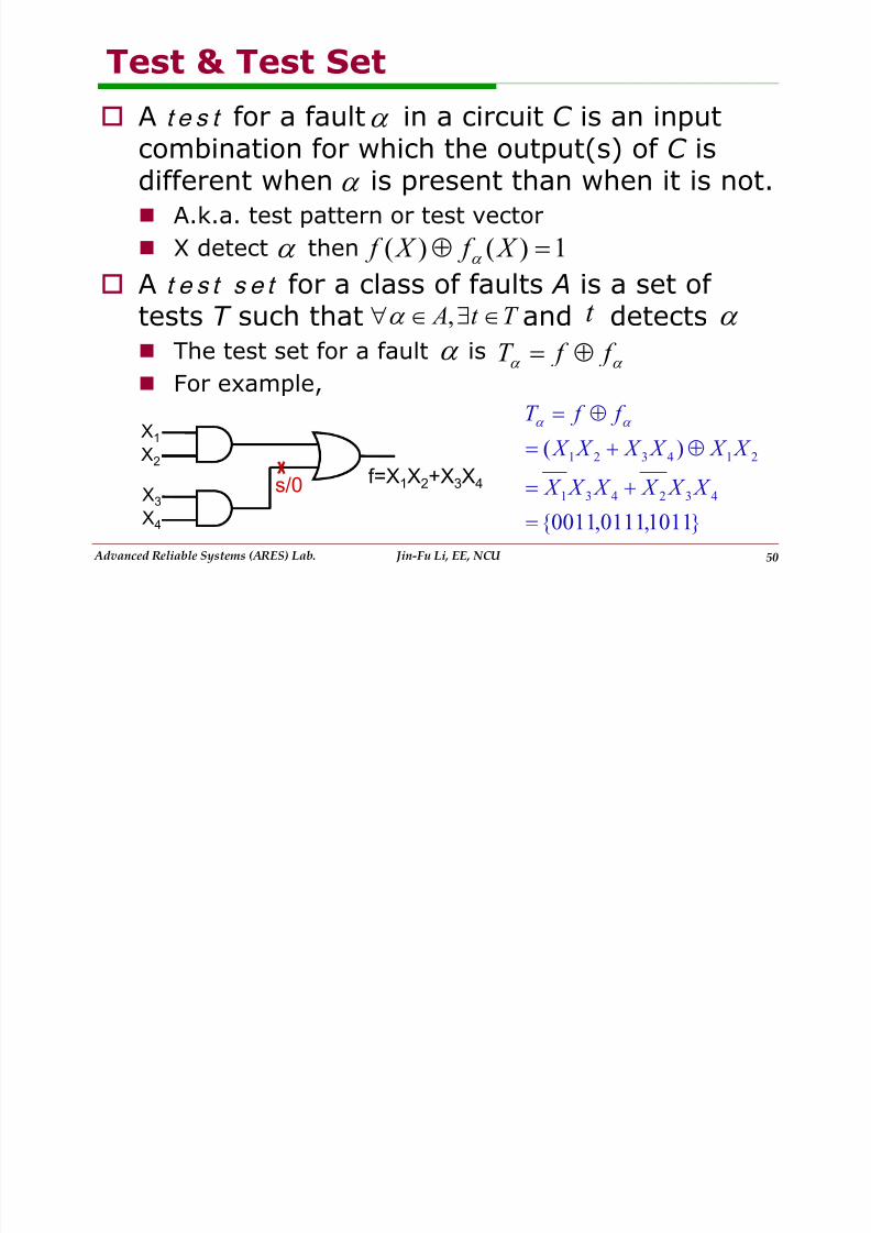
A t e s t for a fault in a circuit C is an inputcombination for which the output(s) of C isdifferent when is present than when it is not.
A.k.a. test pattern or test vector X detect then
A t e s t s e t for a class of faults A is a set oftests T such that and detects
The test set for a fault is
For example,
1)()( X f X f
T t A , t
f f T
X1
X2
X3
X4
f=X1X2+X3X4s/0
}1011,0111,0011{
)(
432431
214321
X X X X X X
X X X X X X
f f T
Testing & Diagnosis
7/17/2019 ch06
http://slidepdf.com/reader/full/ch06563db960550346aa9a9cbebb 51/83
Advanced Reliable Systems (ARES) Lab. Jin-Fu Li, EE, NCU 51
g g
T e s t i n g is a process which includes testpattern generation, test pattern application,and output evaluation.
Fa u l t d e t e c t i o n tells whether a circuit isfault-free or not
Fa u l t l o c a t i o n provides the location of the
detected fault Fa u l t d i a g n o s i s provides the location and the
type of the detected fault
The input X distinguishes a fault from anotherfault iff , i.e.,
1)()( X f X f )()( X f X f
Testing & Diagnosis

7/17/2019 ch06
http://slidepdf.com/reader/full/ch06563db960550346aa9a9cbebb 52/83
Advanced Reliable Systems (ARES) Lab. Jin-Fu Li, EE, NCU 52
g g
Example:
Ca/0 and Cc/0 are detected by the test pattern(1,0)
If we apply two test patterns: (1,0) & (0, 1)
Two corresponding outputs are faultyCc/0
Only the output with respect to the input (1,0) isfaultyCa/0
ab c
ca/0a b c
0 0 00 1 11 0 11 1 1
ca/1 cb/0 cb/1 cc/0 cc/1
0101
11
1
0
10
1
0
010
011
11
11
11
7/17/2019 ch06
http://slidepdf.com/reader/full/ch06563db960550346aa9a9cbebb 53/83
Stuck-At Faults
7/17/2019 ch06
http://slidepdf.com/reader/full/ch06563db960550346aa9a9cbebb 54/83
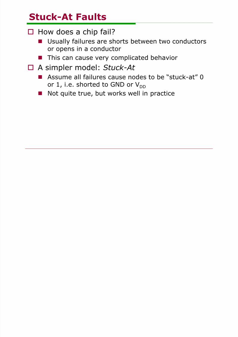
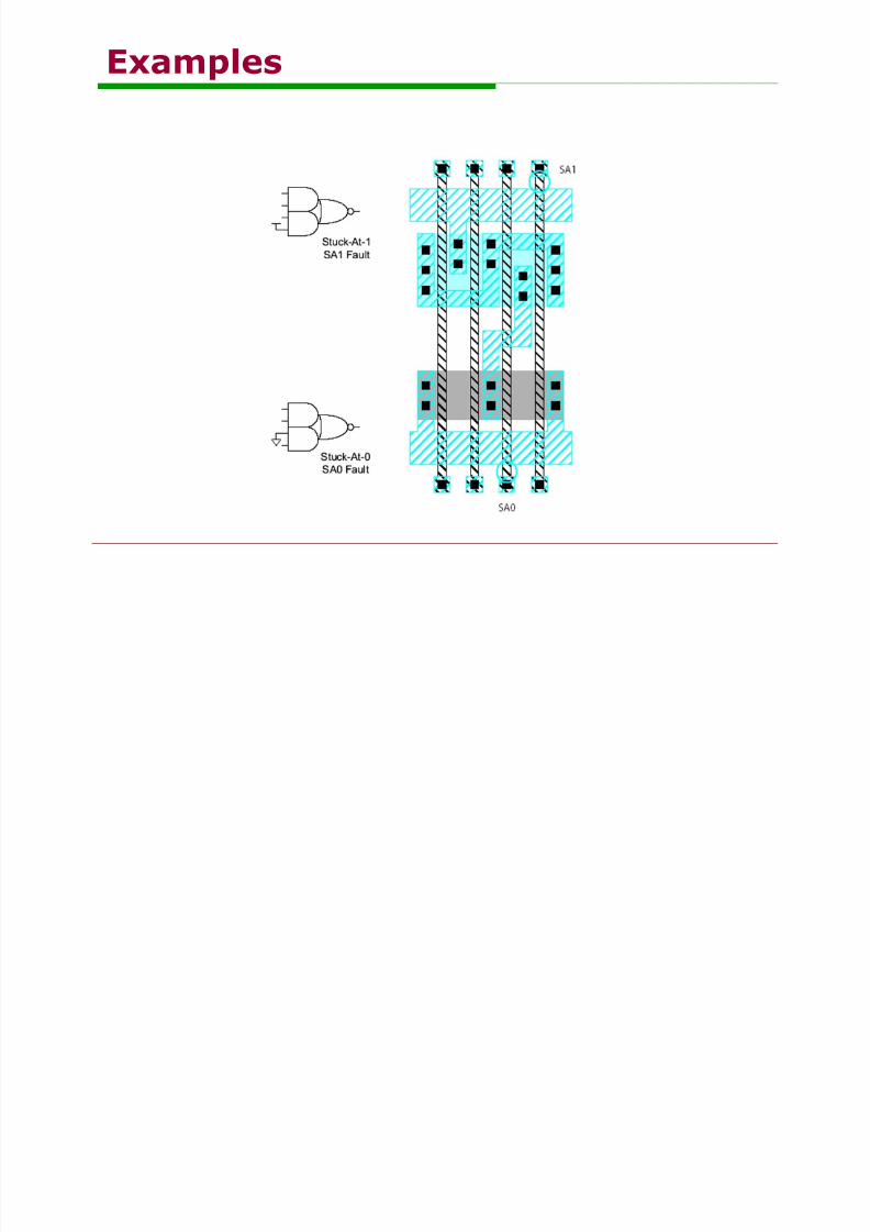
How does a chip fail? Usually failures are shorts between two conductors
or opens in a conductor
This can cause very complicated behavior
A simpler model: Stuck-At
Assume all failures cause nodes to be “stuck-at” 0or 1, i.e. shorted to GND or VDD
Not quite true, but works well in practice
Examples
7/17/2019 ch06
http://slidepdf.com/reader/full/ch06563db960550346aa9a9cbebb 55/83
Observability & Controllability

7/17/2019 ch06
http://slidepdf.com/reader/full/ch06563db960550346aa9a9cbebb 56/83
Observability : ease of observing a node bywatching external output pins of the chip
Controllability : ease of forcing a node to 0 or 1
by driving input pins of the chip
Combinational logic is usually easy to observe
and control Finite state machines can be very difficult,
requiring many cycles to enter desired state
Especially if state transition diagram is not known tothe test engineer

7/17/2019 ch06
http://slidepdf.com/reader/full/ch06563db960550346aa9a9cbebb 57/83
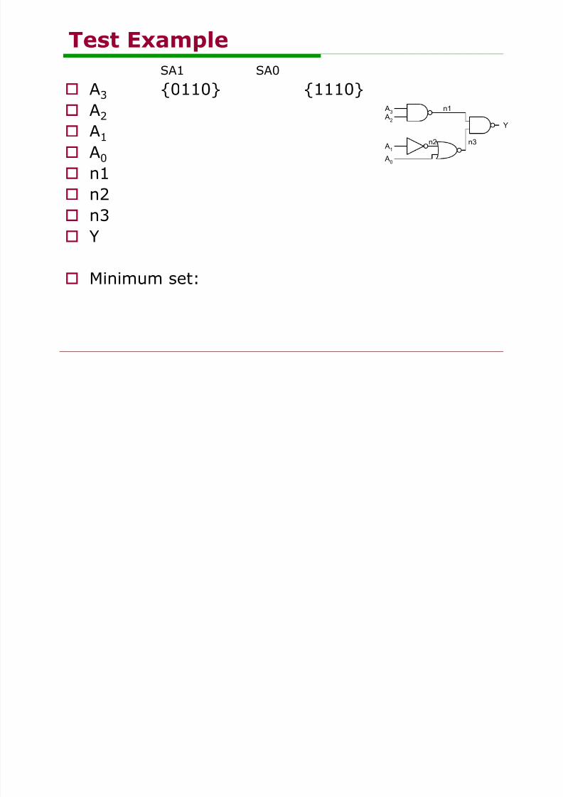
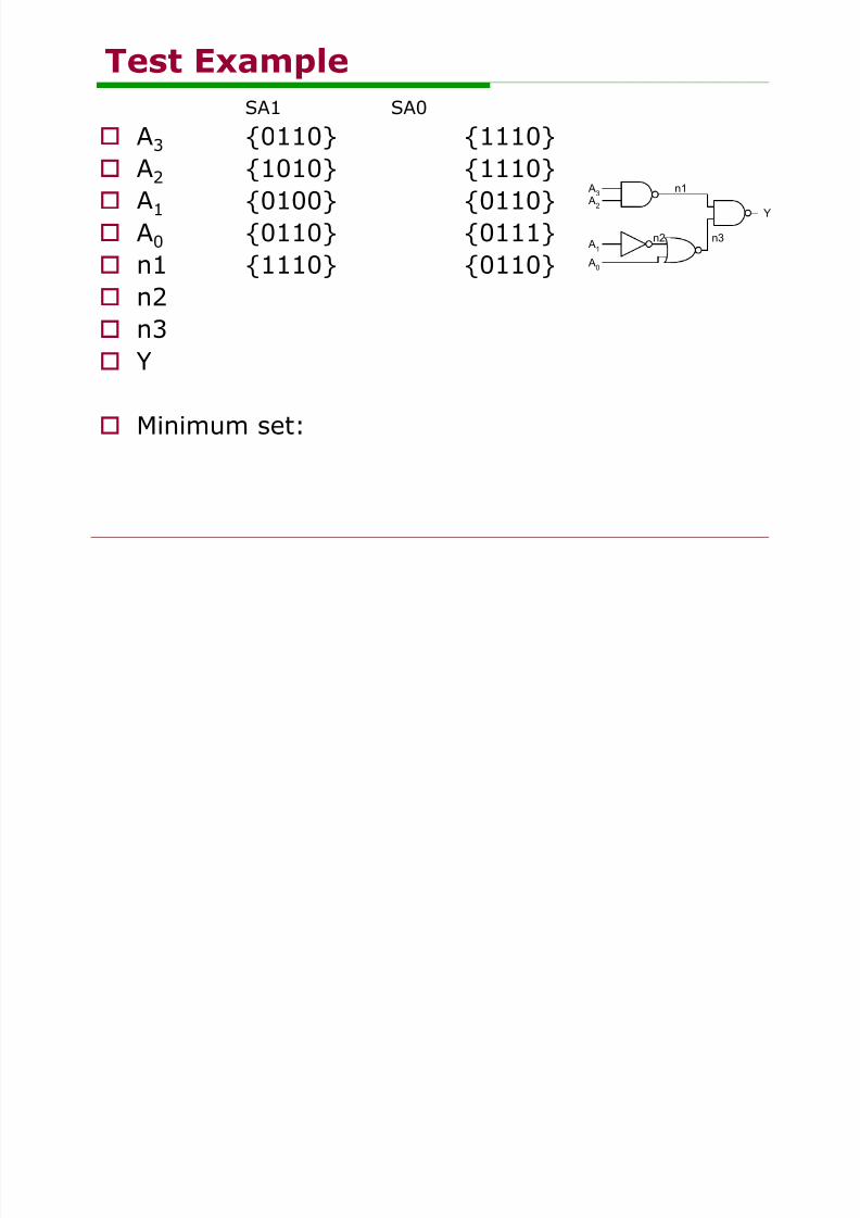
Test Example
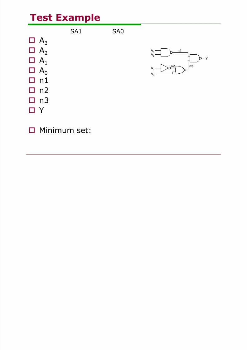
7/17/2019 ch06
http://slidepdf.com/reader/full/ch06563db960550346aa9a9cbebb 58/83
SA1 SA0
A3
A2
A1
A0
n1
n2
n3
Y
Minimum set:
A3
A2
A1
A0
Y
n1
n2 n3
Test Example
7/17/2019 ch06
http://slidepdf.com/reader/full/ch06563db960550346aa9a9cbebb 59/83
SA1 SA0
A3 {0110} {1110}
A2
A1
A0
n1
n2
n3 Y
Minimum set:
A3
A2
A1
A0
Y
n1
n2 n3
Test Example
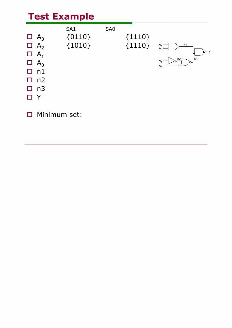
7/17/2019 ch06
http://slidepdf.com/reader/full/ch06563db960550346aa9a9cbebb 60/83
SA1 SA0
A3 {0110} {1110}
A2 {1010} {1110}
A1
A0
n1
n2
n3 Y
Minimum set:
A3
A2
A1
A0
Y
n1
n2 n3
Test Example
7/17/2019 ch06
http://slidepdf.com/reader/full/ch06563db960550346aa9a9cbebb 61/83
SA1 SA0
A3 {0110} {1110}
A2 {1010} {1110}
A1 {0100} {0110}
A0
n1
n2
n3 Y
Minimum set:
A3
A2
A1
A0
Y
n1
n2 n3
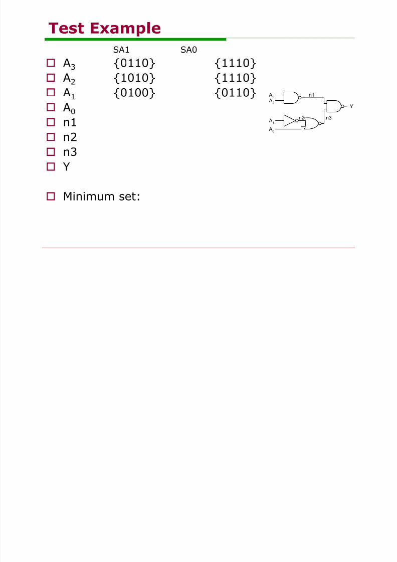
Test Example
7/17/2019 ch06
http://slidepdf.com/reader/full/ch06563db960550346aa9a9cbebb 62/83
SA1 SA0
A3 {0110} {1110}
A2 {1010} {1110}
A1 {0100} {0110}
A0 {0110} {0111} n1
n2
n3 Y
Minimum set:
A3
A2
A1
A0
Y
n1
n2 n3
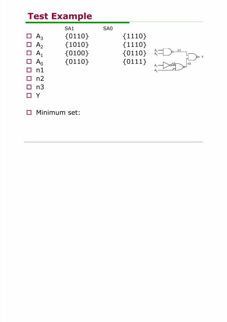
Test Example
7/17/2019 ch06
http://slidepdf.com/reader/full/ch06563db960550346aa9a9cbebb 63/83
SA1 SA0
A3 {0110} {1110}
A2 {1010} {1110}
A1 {0100} {0110}
A0 {0110} {0111} n1 {1110} {0110}
n2
n3 Y
Minimum set:
A3
A2
A1
A0
Y
n1
n2 n3
Test Example
7/17/2019 ch06
http://slidepdf.com/reader/full/ch06563db960550346aa9a9cbebb 64/83
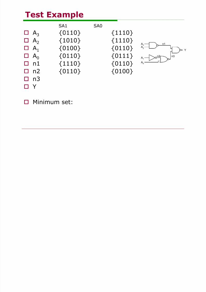
SA1 SA0
A3 {0110} {1110}
A2 {1010} {1110}
A1 {0100} {0110}
A0 {0110} {0111} n1 {1110} {0110}
n2 {0110} {0100}
n3 Y
Minimum set:
A3
A2
A1
A0
Y
n1
n2 n3
Test Example
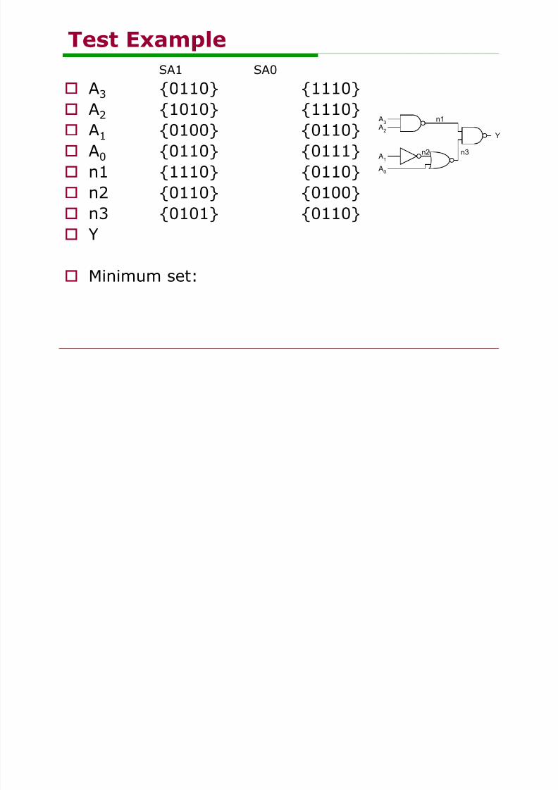
7/17/2019 ch06
http://slidepdf.com/reader/full/ch06563db960550346aa9a9cbebb 65/83
SA1 SA0
A3 {0110} {1110}
A2 {1010} {1110}
A1 {0100} {0110}
A0 {0110} {0111} n1 {1110} {0110}
n2 {0110} {0100}
n3 {0101} {0110} Y
Minimum set:
A3
A2
A1
A0
Y
n1
n2 n3
Test Example
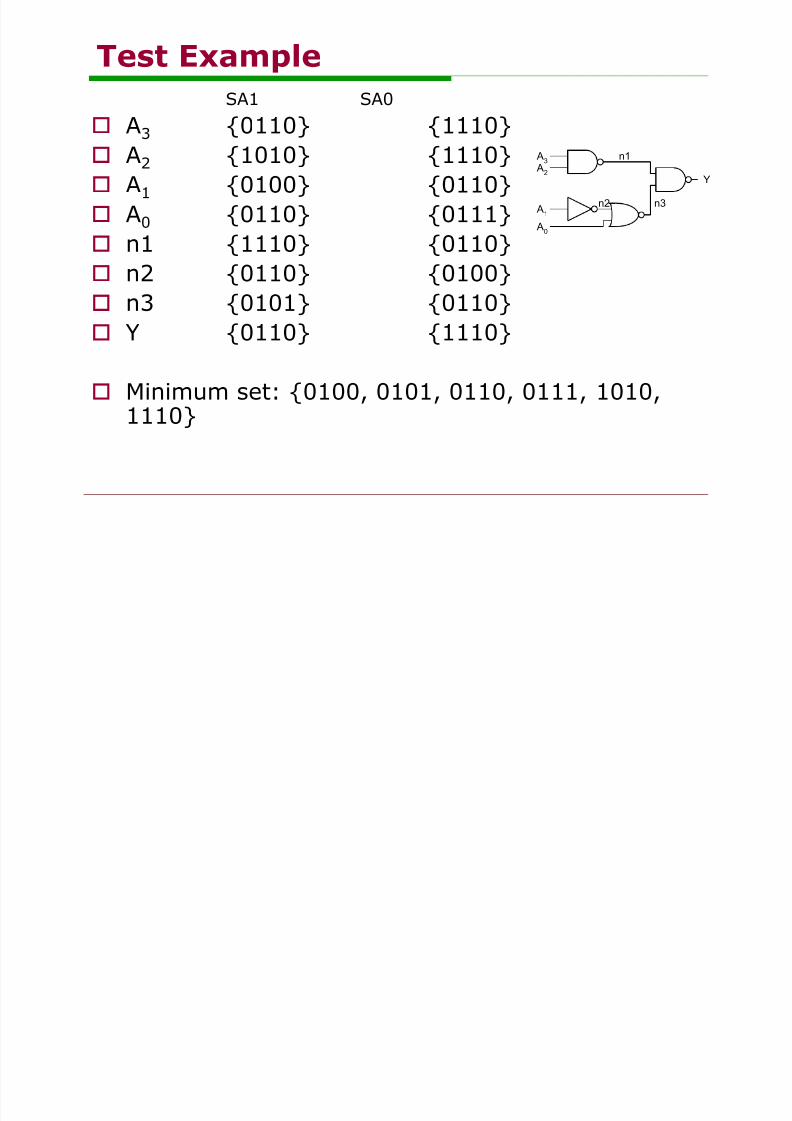
7/17/2019 ch06
http://slidepdf.com/reader/full/ch06563db960550346aa9a9cbebb 66/83
SA1 SA0
A3 {0110} {1110}
A2 {1010} {1110}
A1 {0100} {0110}
A0 {0110} {0111} n1 {1110} {0110}
n2 {0110} {0100}
n3 {0101} {0110} Y {0110} {1110}
Minimum set: {0100, 0101, 0110, 0111, 1010,1110}
A3
A2
A1
A0
Y
n1
n2 n3
Design for Test

7/17/2019 ch06
http://slidepdf.com/reader/full/ch06563db960550346aa9a9cbebb 67/83
Design the chip to increase observability andcontrollability
If each register could be observed andcontrolled, test problem reduces to testingcombinational logic between registers.
Better yet, logic blocks could enter test modewhere they generate test patterns and reportthe results automatically.
Scan
7/17/2019 ch06
http://slidepdf.com/reader/full/ch06563db960550346aa9a9cbebb 68/83
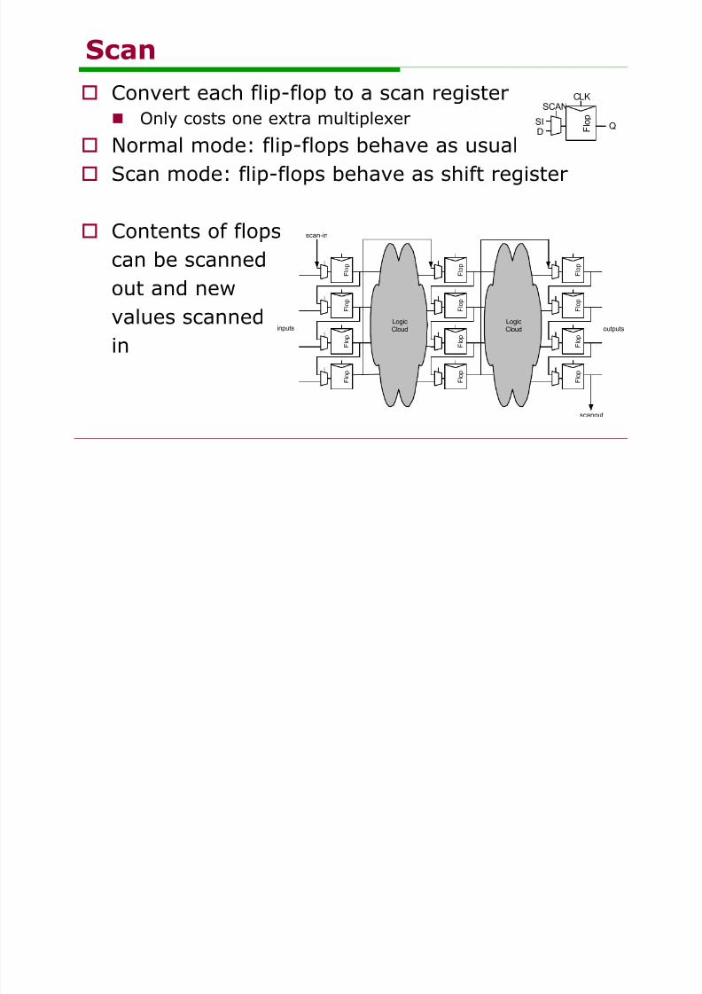
Convert each flip-flop to a scan register Only costs one extra multiplexer
Normal mode: flip-flops behave as usual
Scan mode: flip-flops behave as shift register
Contents of flops
can be scanned
out and new
values scanned
in
F l o p
QD
CLK
SI
SCAN
scanout
scan-in
inputs outputs
F
l o p
F l o p
F l o p
F l o p
F
l o p
F l o p
F l o p
F l o p
F
l o p
F l o p
F l o p
F l o p
LogicCloud
LogicCloud
Scannable Flip-flops
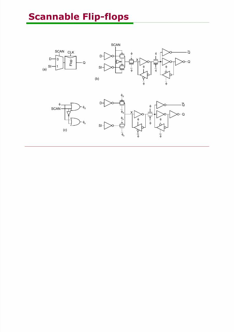
7/17/2019 ch06
http://slidepdf.com/reader/full/ch06563db960550346aa9a9cbebb 69/83
0
1 F l o
p
CLK
D
SI
SCAN
Q
D
X
Q
Q
(a)
(b)
SCAN
SI
D
X
Q
Q
SI
s
s
(c)
d
d
d
s
SCAN
Built-in Self-test

7/17/2019 ch06
http://slidepdf.com/reader/full/ch06563db960550346aa9a9cbebb 70/83
Built-in self-test lets blocks test themselves Generate pseudo-random inputs to comb. logic
Combine outputs into a syndrome
With high probability, block is fault-free if itproduces the expected syndrome
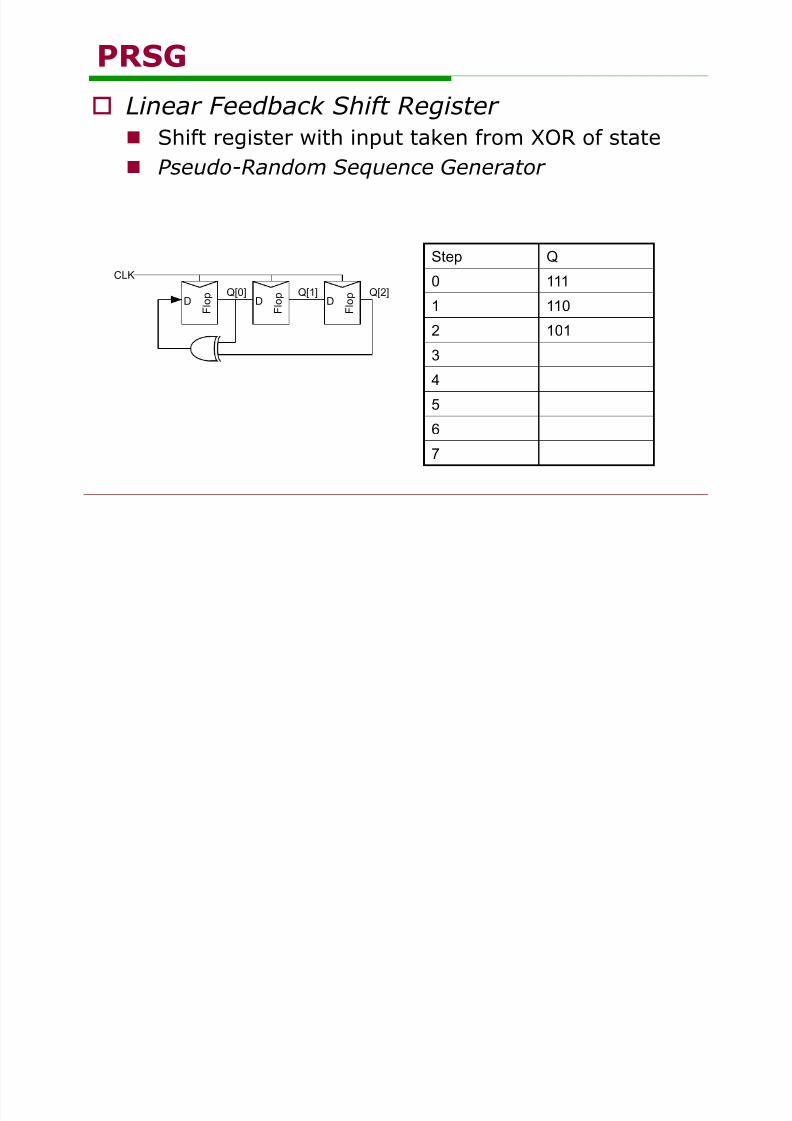
PRSG

7/17/2019 ch06
http://slidepdf.com/reader/full/ch06563db960550346aa9a9cbebb 71/83
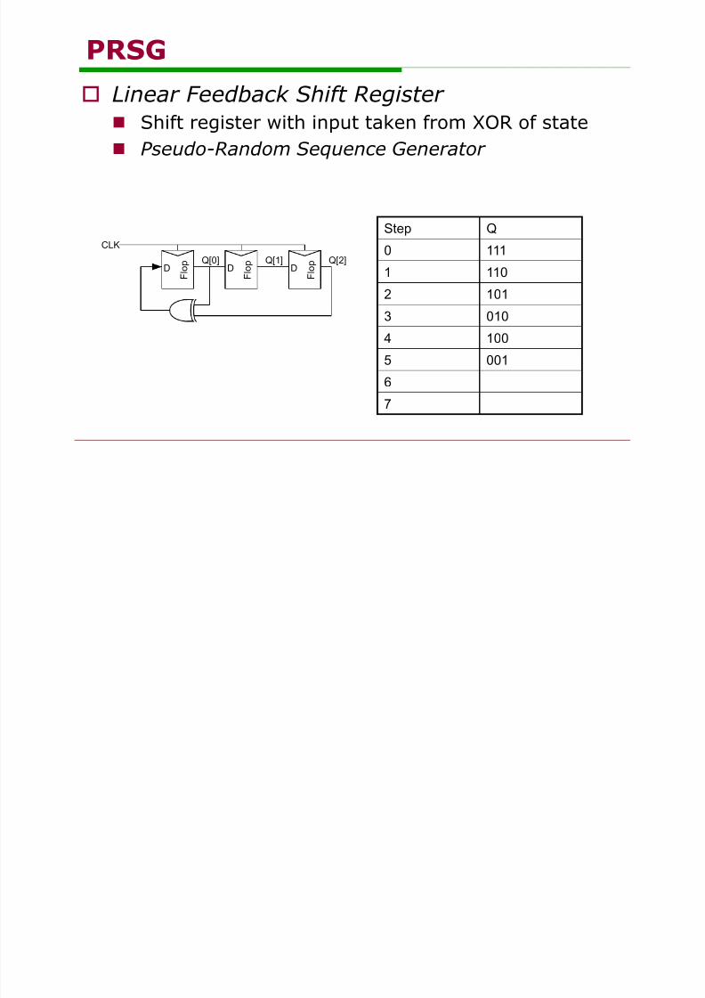
Linear Feedback Shift Register Shift register with input taken from XOR of state
Pseudo-Random Sequence Generator
F
l o p
F
l o p
F
l o pQ[0] Q[1] Q[2]
CLK
D D D
Step Q
0 111
12
3
4
56
7
PRSG

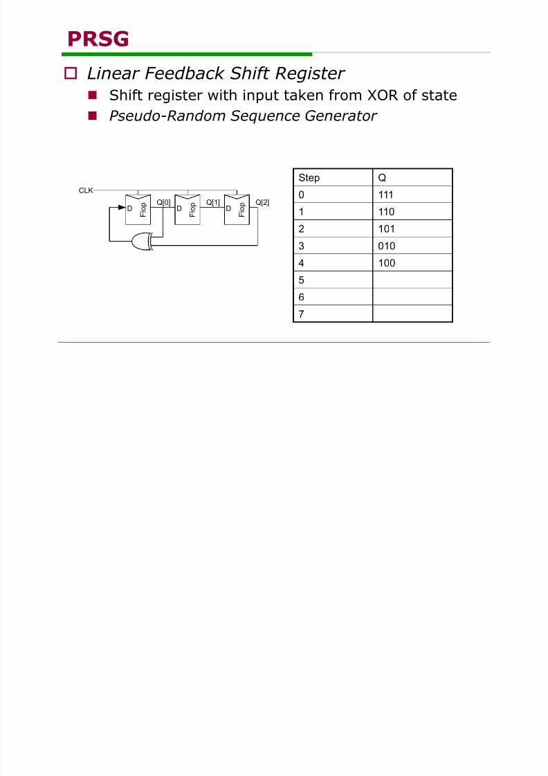
7/17/2019 ch06
http://slidepdf.com/reader/full/ch06563db960550346aa9a9cbebb 72/83
Linear Feedback Shift Register Shift register with input taken from XOR of state
Pseudo-Random Sequence Generator
F
l o p
F
l o p
F
l o pQ[0] Q[1] Q[2]
CLK
D D D
Step Q
0 111
1 1102
3
4
56
7
PRSG
7/17/2019 ch06
http://slidepdf.com/reader/full/ch06563db960550346aa9a9cbebb 73/83
Linear Feedback Shift Register Shift register with input taken from XOR of state
Pseudo-Random Sequence Generator
F
l o p
F
l o p
F
l o pQ[0] Q[1] Q[2]
CLK
D D D
Step Q
0 111
1 1102 101
3
4
56
7
PRSG

7/17/2019 ch06
http://slidepdf.com/reader/full/ch06563db960550346aa9a9cbebb 74/83
Linear Feedback Shift Register Shift register with input taken from XOR of state
Pseudo-Random Sequence Generator
F
l o p
F
l o p
F
l o pQ[0] Q[1] Q[2]
CLK
D D D
Step Q
0 111
1 1102 101
3 010
4
56
7
PRSG
7/17/2019 ch06
http://slidepdf.com/reader/full/ch06563db960550346aa9a9cbebb 75/83
Linear Feedback Shift Register Shift register with input taken from XOR of state
Pseudo-Random Sequence Generator
F
l o p
F
l o p
F
l o pQ[0] Q[1] Q[2]
CLK
D D D
Step Q
0 111
1 1102 101
3 010
4 100
56
7
PRSG
7/17/2019 ch06
http://slidepdf.com/reader/full/ch06563db960550346aa9a9cbebb 76/83
Linear Feedback Shift Register Shift register with input taken from XOR of state
Pseudo-Random Sequence Generator
F
l o p
F
l o p
F
l o pQ[0] Q[1] Q[2]
CLK
D D D
Step Q
0 111
1 1102 101
3 010
4 100
5 0016
7
PRSG

7/17/2019 ch06
http://slidepdf.com/reader/full/ch06563db960550346aa9a9cbebb 77/83
Linear Feedback Shift Register Shift register with input taken from XOR of state
Pseudo-Random Sequence Generator
F
l o p
F
l o p
F
l o pQ[0] Q[1] Q[2]
CLK
D D D
Step Q
0 111
1 1102 101
3 010
4 100
5 0016 011
7
PRSG

7/17/2019 ch06
http://slidepdf.com/reader/full/ch06563db960550346aa9a9cbebb 78/83
Linear Feedback Shift Register Shift register with input taken from XOR of state
Pseudo-Random Sequence Generator
F
l o p
F
l o p
F
l o pQ[0] Q[1] Q[2]
CLK
D D D
Step Q
0 111
1 1102 101
3 010
4 100
5 0016 011
7 111 (repeats)
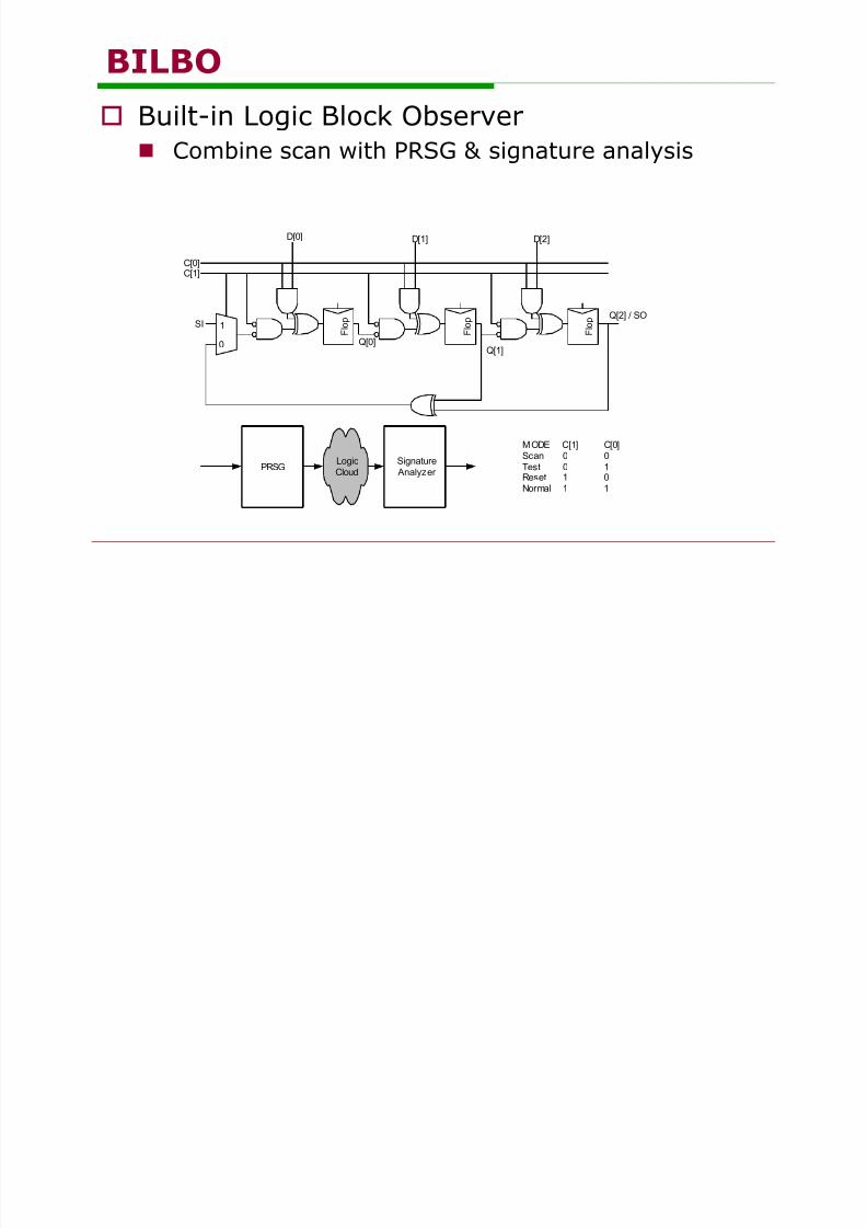
BILBO
7/17/2019 ch06
http://slidepdf.com/reader/full/ch06563db960550346aa9a9cbebb 79/83
Built-in Logic Block Observer Combine scan with PRSG & signature analysis
MODE C[1] C[0]Scan 0 0
Test 0 1Reset 1 0Normal 1 1
F l o p
F l o p
F l o p
1
0
D[0] D[1] D[2]
Q[0]Q[1]
Q[2] / SOSI
C[1]C[0]
PRSGLogic
Cloud
Signature
Analyzer
Boundary Scan

7/17/2019 ch06
http://slidepdf.com/reader/full/ch06563db960550346aa9a9cbebb 80/83
Testing boards is also difficult Need to verify solder joints are good
Drive a pin to 0, then to 1
Check that all connected pins get the values
Through-hold boards used “bed of nails”
SMT and BGA boards cannot easily contactpins
Build capability of observing and controllingpins into each chip to make board test easier
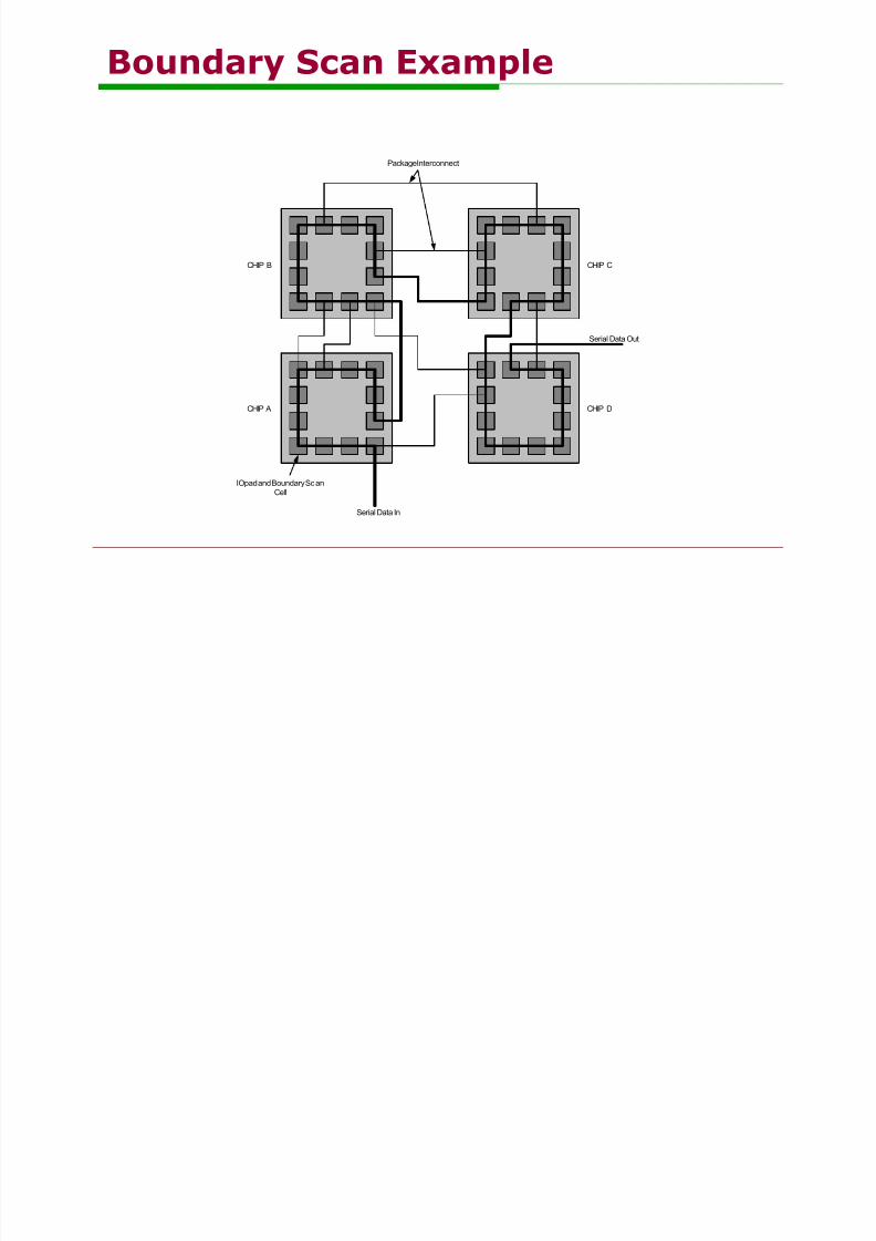
Boundary Scan Example
7/17/2019 ch06
http://slidepdf.com/reader/full/ch06563db960550346aa9a9cbebb 81/83
Serial Data In
Serial Data Out
PackageInterconnect
IO pad and Boundary ScanCell
CHIP A
CHIP B CHIP C
CHIP D
Boundary Scan Interface

7/17/2019 ch06
http://slidepdf.com/reader/full/ch06563db960550346aa9a9cbebb 82/83
Boundary scan is accessed through five pins TCK: test clock
TMS: test mode select
TDI: test data in
TDO: test data out
TRST*: test reset (optional)
Chips with internal scan chains can access thechains through boundary scan for unified teststrategy.
Summary

7/17/2019 ch06
http://slidepdf.com/reader/full/ch06563db960550346aa9a9cbebb 83/83
Think about testing from the beginning Simulate as you go
Plan for test after fabrication
“If you don’t test it, it won’t work!(Guaranteed)”