ccem strategic plan - bipm · pdf fileccem strategic plan . ... because of the distinct...
TRANSCRIPT

V5.3 26/03/2014
CCEM strategic plan This CCEM strategic plan was prepared by a small drafting team, including the WGLF and GT-RF chairmen. It was presented to the CCEM in March 2013 and this version includes comments arising from that discussion. 1. General Information on CC Body (CC or a CC WG): CC Name: Consultative Committee on Electricity and Magnetism (CCEM) CC Working Groups: Low Frequency Working Group (WGLF); Working Group on Radiofrequency Quantities (Groupe de Travail pour les grandeurs aux Radio-Fréquences, GT-RF), Working group on RMO coordination (WGRMO), Working group on electrical methods to monitor the stability of the kilogram (WGKG), Working group on the SI (WGSI) Date Established: 1927 Number of Members: 23 Number of Participants at last meeting: 36 delegates and experts from member NMIs Periodicity between Meetings: 2 years Date of last meeting: March 2013 WGLF Chair: Dr. Jonathan Williams, NPL, chair since 2008 GT-RF Chair: Dr. James Randa, NIST, chair 2002-2013 Dr. Markus Zeier, METAS, chair since March 2013 WGRMO Chair: Dr. François Piquemal, LNE, chair since 2013 WGKG Chair: Dr. Ian Robinson, NPL, chair since 2000 WGSI Chair: Dr. Barry Wood, NRC, chair since 2006 Number of KCs organized (from 1999 up to and including 2012):
15 distinct WGLF KCs completed 2 WGLF KCs are presently active 11 GT-RF KCs completed 6 GT-RF KCs are presently active
A total of 60 key and 2 supplementary CIPM comparisons (including pre-MRA comparisons “approved for provisional equivalence”) are listed in the KCDB for electricity and magnetism. The key and supplementary comparisons listed for the Regional Metrology Organisations in the KCDB at March 2013 are summarized in the following table:
Number of CMCs published in KCDB supported by CC body activities (up to and including 2012): 7062 individual CMCs from 52 countries are recorded in the area of electricity and magnetism (CCEM) as of October 2012. This includes contributions from both the low and high frequency regimes (determining the split between the two regimes is difficult), spanning 12 main categories, subdivided in 48 subcategories and 192 sub-subcategories. This is the largest number of CMCs and categories in any technical area, and is indicative of the extremely broad parameter space covered, and the wide interest in this area by most NMIs of the world.
Region Key Supplementary EURAMET 24 36 APMP 18 15 SIM 15 10 COOMET 5 16 AFRIMETS - -
1

V5.3 26/03/2014
The maintenance of this data is a significant and important task and is carried out very effectively by the BIPM. The CCEM supports the concept of improving the capabilities of the KCDB to reduce the effort required for CMC reviews. 2. Terms of Reference
The CCEM has two standing working groups that are each responsible for a different frequency range for electromagnetic measurements: the Working Group on Low Frequency Quantities (WGLF) and the Working Group on Radiofrequency Quantities (Groupe de Travail pour les grandeurs aux Radio-Fréquences, GT-RF). Splitting the frequency spectrum is necessary because of the vastly different technologies required for each range of measurements. No practical realization of the SI unit of current presently exists, so the WGLF and GT-RF are responsible for maintaining the equivalence of the SI base and the derived electrical units, and organizing, conducting, and approving key comparisons of the corresponding quantities over a wide range of magnitudes and frequencies. Because of the distinct planning differences between the two working groups in CCEM, much of the content of this document is split between the two frequency regimes.
The WGLF is the CCEM working group for low frequency electrical metrology, defined as dc to the MHz region. It essentially covers the seven “derived” electrical quantities of voltage, resistance, capacitance, inductance, power, voltage ratios, and ac/dc difference. It also advises the CCEM and its other working groups on metrology matters related to low frequency electrical metrology. While in practice the WGLF also supports the area of magnetism, this has not been an area of significant effort and has resulted in only a single key comparison.
The GT-RF is the CCEM working group for radiofrequency and microwave (RF/MW) frequencies, defined as the MHz region and above. It organizes, conducts, and approves key comparisons at these frequencies. It also advises the CCEM and other CCEM working groups on matters related to radiofrequency and microwave frequencies.
The CCEM also has a standing Working Group for RMO Coordination (WGRMO) and a number of focused working groups formed to foster international cooperation on particular technical topics that are of importance to the CCEM member economies. At present these are the Working Group on Electrical Methods to Monitor the Stability of the Kilogram (WGKG) and the Working Group on Proposed Modifications to the SI (WGSI). The WGKG and WGSI specifically address the topic of the proposed re-definition of the SI in which the electrical quantum effects play a central role. The CCEM previously commissioned a working group to coordinate research on the quantized Hall effect with alternating current (WGACQHR) with the aim of sharing devices, knowledge and techniques to gain a common understanding of the metrological issues. The research results were published in several scientific papers and the working group concluded with a final report to the CCEM in 2011.
3. Major issues/challenges for the CCEM The major technical challenges for the CCEM have been identified in the “Big Problems in Electromagnetics”, CCEM Strategic Planning Document (Appendix A), of which a few are highlighted here:
• Reducing the workload related to the CIPM MRA in a field with many derived quantities, often extending over a large range of values by the design of efficient Key Comparisons and delegation to the regions to run further Key and Supplementary Comparisons according to need. Further significant reduction of the workload can be achieved by increasing the efficiency of the CMC review and maintenance process, as already indicated at the end of the first section, for example by improving the capabilities of the KCDB, reduction of the number of (sub)subcategories, and the increased use of matrices.
2

V5.3 26/03/2014
• Support technological developments in electrical instrumentation by making quantum standards more versatile and more widely available, develop acJVS and acQHR standards, develop new generation of simpler QHR standards based on graphene samples, continue development of quantum current standards using SET devices.
• Support electrical measurement in the rapidly growing field of power and energy metrology and important new fields such as nanometrology and THz metrology
• Manage the expected change of magnitude of the electrical units, in particular the volt (potentially more than 1 part in 107), caused by the redefinition, which will be significant for some stakeholders.
4. Baseline (description status of activities and achievements up to and including 2012) A description of what the body has achieved since 1999 including the total number of comparisons and CMCs supported. Discussions of major changes in needs, technologies or areas of interest during the period and the effect on the activities of the body. Major challenges and difficulties encountered and issues that require resolution. Information on repeat frequencies of any comparisons to date.
Since 1999, the WGLF has essentially completed 15 key comparisons covering the electrical areas of voltage, resistance, capacitance, inductance, power, voltage ratios, ac/dc difference, and magnetism. The BIPM is organizing 5 ongoing comparisons, including two on-site comparisons of quantum standards. Electrical metrology naturally covers a large number of diverse technical areas with extraordinarily broad ranges of the parameter spaces. For example, resistance calibrations cover 20 orders of magnitude, and measurements of ac/dc difference range from Hz to 100 MHz, from mA to 100 A, from mV to 1000 V. Because of this nearly infinite parameter space, the WGLF evaluated the vast array of potential comparisons at low frequencies and carefully chose the ones that most effectively, efficiently, and responsibly demonstrate the capabilities of the participating NMIs. Thus, for example, two carefully chosen key comparisons for resistance demonstrate competence over most of the possible range of resistance. Five distinct comparisons adequately cover the multifaceted parameter space of ac/dc difference, and one comparison each at cardinal points cover capacitance, inductance, and electric power.
While there have been many advances in low frequency electrical metrology since 1999, none has impacted the international community sufficiently to merit serious consideration of additional comparisons in “new” areas. The one possible exception is the just beginning comparison (K13) of non-sinusoidal waveforms (at 120 V and 5 A) in response to the needs of smart metering. To date, no key comparison has been repeated by the WGLF. However, some of the results are approaching 15 years old, and incremental improvements in capabilities (mostly lower uncertainties) now make it necessary to repeat the comparisons of most (if not all) of these fundamental measurements. For example, the degrees of equivalence of a recent regional comparison had to be increased due to the larger uncertainties claimed by the linking NMIs in the CCEM key comparison completed many years ago. While there appears to be general agreement that low frequency electrical comparisons should be repeated on approximately a 10 year cycle, there are presently distinct barriers to the WGLF members enthusiastically starting the process of repeating key comparisons. The barriers include 1) a sense of lack of resources by the participating NMIs to fulfill the requirements, especially for pilot laboratories; 2) that the technical benefits of the key comparison are not universally accepted; and 3) the fear that bringing a comparison to completion will be extremely difficult (this is based upon the recollections of early key comparisons). Overcoming these barriers within the WGLF will require significant planning to ensure efficient performance of the comparisons with a careful sharing of responsibilities across several NMIs.
3

V5.3 26/03/2014
Since 1999, the GT-RF has completed 9 key comparisons that had been begun before 1999, and it has undertaken 12 new key comparisons and one new pilot study. The GT-RF identified seven ‘key quantities’ on which key comparisons will be conducted, and it adopted a policy of conducting no more than one key comparison at a time on each key quantity. The seven key quantities are: power, scattering parameters and impedance, noise power, voltage, attenuation, electromagnetic field strength, and antenna parameters. There has been more than one key comparison on several of the key quantities, but in such cases the different key comparisons have covered different frequency bands. To date, no key comparison has been repeated.
During the 1999 – 2012 time period, the GT-RF has seen a decrease in the need for further comparisons in the area of traditional voltage measurements, due to the maturity of the field and the absence of new technologies. However, there has been increased interest and activity in waveform measurements, particularly on-wafer measurements and measurements at higher frequencies (extending above 100 GHz). The interest in waveform measurements is driven in large part by demand for traceable measurements of digital signal properties. This interest is evidenced, for example, by the current EMRP project “Metrology for Ultrafast Electronics and High-Speed Communications,” which focuses on this topic and includes seven European NMIs. There has also been increased interest in measurement of the electromagnetic properties of materials, and the GT-RF recently began a pilot study in EM properties of materials. 5. Stakeholders (who they are and their level of involvement) A list and/or description of who are the end-user beneficiaries and whether (and if so how) they are involved in identifying measurement needs, and in prioritization, particularly for comparisons.
The immediate beneficiaries are the CCEM-member NMIs that participate in international metrology activities such as key comparisons. They gain confirmation of the soundness of their standards and measurements, or identify weaknesses in them. Based on the ever evolving traceability needs from industry, the member NMIs identify and prioritize measurement and comparison needs in the regular official and informal WGLF and GT-RF meetings. The CCEM key comparisons underpin the key and supplementary comparison programs conducted by the Regional Metrology Organisations, which in turn provide the basis for a coherent and proven international system of measurement. This enables the regions to build their industrial calibration capabilities on a solid infrastructure and ultimately benefits the industries and economies of all member States.
In 2008, a specially formed Working Group of the CCEM for Strategic Planning produced a document summarizing the “Big” Problems in Electromagnetics (see Appendix A), which was updated in May 2011. The Working Group was formed to both identify the major future problems challenging the National Metrology Institutes in electromagnetic metrology and to provide input to the CCEM on the BIPM’s technical program on electrical metrology. The document considers topics relevant to the medium (5-10 year) term such as the practical realization of a quantum current standard based on single electron transport, the measurement of the kilogram in terms of the Planck constant following the planned redefinition of the SI and the realization of ac as well as dc quantities using the Josephson effect. It also gives a perspective on longer term scientific topics and their bearing on the CCEM. These include quantum computing with superconducting Qubits, nano-bioelectronics, molecular electronics, electromagnetic metrology at the nanoscale and spintronics, nanomagnetism and THz metrology. The emerging technology of single photonics is also discussed where there is overlap with the CCPR.
As the scope of electromagnetic measurements, in terms of frequency, spatial resolution and sensitivity, continues to evolve, the CCEM will need to engage with new technical communities requiring metrology support.
4

V5.3 26/03/2014
6. Future Scan (2013-2023) A future vision of the landscape and consequent requirements and measurement challenges, identifying: likely ongoing requirements; requirements that will appear or develop in the next 10 years, particularly identifying potential major/disruptive step changes.
The importance of key comparisons will not diminish in the coming decade. They ensure ongoing consistent realization of the SI, they demonstrate continued competence in the NMIs, and they support improved measurement uncertainties as the demand for better measurements increases over time. Thus, it appears likely that activity and comparisons in the seven key quantities identified by each working group will continue to be the most important areas of concern. This is not surprising since these quantities were chosen initially because they underpin virtually all electromagnetic measurements and link these measurements to the SI. It is expected that the primary focus of the WGLF and the GT-RF will continue to be the organization of key comparisons for these quantities. Even if the methods of realizing or measuring these quantities were to change significantly, the measurement protocols most likely will not evolve significantly.
The importance of the development of quantum standards cannot be overstated in the area of electrical measurements in the low frequency regime. In fact, the deployment of such standards offers the possibility of eliminating the need for certain key comparisons. For example, the capability for direct comparisons for Josephson voltage systems, offered by BIPM and some NMIs within their regions, essentially eliminates the need for a CCEM key comparison of Zener voltage standards. (The BIPM, however, proposes an ongoing key comparison of Zener voltage standards for NMIs which do not possess a Josephson voltage standard and as a first step before an on-site Josephson voltage comparison). In a similar way, the need for a 100 Ω resistance key comparison is significantly diminished by the now widespread use of quantized Hall resistance standards. The development of higher temperature quantum Hall standards based upon graphene technologies, opens the possibility of less complex QHR systems and a more widespread use of the QHR in the future. On the request of the CCEM, the BIPM is resuming the ongoing on-site key comparison of quantized Hall resistance standards to support this development and wider use. There continues to be the excellent potential for a quantum current standard based upon some version of single electron tunneling effects. There are also continued advances being made in developing new applications of Josephson voltage standards, particularly in the areas of ac power and ac voltage. New comparisons in these two areas might be required of the WGLF if they become the new standard of realization within the NMIs.
A rapidly growing area that may require metrological support at the CCEM level is transmission and distribution of electrical energy. Smart Grids and new ultra-high voltage transmission, both dc and ac, are some of the factors contributing to the growth for metrology research. The corresponding quantities for which comparisons may be necessary are harmonic power, voltage and current phasors (synchrophasor measurements), current ratios up to 20 kA, voltage ratios up to 1000 kV (dc and ac), and characteristics of switching and lightning impulses. Some of these comparisons are presently organized by RMOs and individual labs. However, extension of this work to the CCEM may be necessary to ensure world-wide traceability.
Dynamic measurements based on digital sampling where parameters are changing rapidly in time are, generally, a potential area of increased activity. Precision measurement of rapidly varying quantities is of growing interest to industry where real time measurements are required for process control and for in-line testing. Thus in the future it is conceivable that comparisons for voltage or current waveforms, or for rapidly varying values of resistance or capacitance as found in sensors for dynamic quantities, may become an important issue for CCEM consideration.
While the proposed redefinition of the SI does not directly suggest any significant technological challenges in the area of electromagnetic measurements, the anticipated need for the development of “routine operation” watt balances will require the development of more economical and reliable electrical standards with the lowest possible uncertainties. The need for precision electromagnetic measurements to realize mass will necessarily demand a continuing CCEM role. Additionally, the potential development of a true quantum current standard opens up exciting new
5

V5.3 26/03/2014
possibilities for realization of the SI, and the CCEM will play a significant role in this arena as well.
In the RF/MW regime, new comparisons in each of the seven key quantities will be required at higher frequencies as the importance of higher frequencies increases and more labs acquire measurement capabilities at higher frequencies. Already completed comparisons will not be repeated unless new techniques or problems emerge.
One possible exception for continuing key quantities is RF voltage. Although there is still demand for voltage calibrations at the lower RF/MW frequencies, these frequencies have been covered by completed comparisons, and there does not seem to be much need for comparisons of traditional voltage measurements at higher frequencies. Instead, the interest and activity has shifted to waveform measurements. Over the next ten years, it is reasonable to expect that “voltage” comparisons will morph into waveform measurement comparisons at higher frequencies.
Another area in which increased activity may be needed is in the electromagnetic properties of materials. The GT-RF is currently conducting a pilot study in this area, and it is possible that subsequent activity may be needed. Other emerging areas include RF/MW measurements on nano-materials, nonlinear and multifunctional devices, on-wafer measurements, and brightness-temperature (RF/MW spectral radiance) measurements. The area of terahertz measurements will also see increased activity, but that is included in the move to higher frequencies.
It is expected that BIPM will continue to have no RF/MW activity, and consequently all the emerging requirements will have to be met by the NMIs and by private industry. 7. Rationale for various activities (2013-2023) A rationale for the research and development activities, measurement services and the selection basis for comparisons (including statements on ‘how far the light shines’) that are foreseen over the period, indicating the time periods when these different activities will be required.
As in every area of metrology, the rationale for research and development activities and measurements services is set by the individual NMIs, based on requests from industry for particular quantities and on general information regarding emerging metrology requirements. As sufficient worldwide interest develops in a particular electromagnetic area that has international metrology implications, the area of research will be discussed in the appropriate CCEM working group. If a more orchestrated effort is called for across many NMIs, a special ad hoc working group may be formed to foster collaboration, develop standard measurement procedures, or recommend new key comparisons. Any of the developing areas mentioned in Section 6 of this report might rise to this level, but that is unpredictable at this time.
As mentioned earlier, the extremely broad range of parameters within the electromagnetic area requires careful evaluation and selection of key comparisons to place a limit on the total number of required comparisons. Thus, by necessity, the “light shines” very far in the CCEM. This philosophy was discussed early on by the WGLF and the GT-RF after the signing of the MRA, and it is still generally agreed that the comparisons completed to date provide a sufficient infrastructure for the NMIs of the world to demonstrate basic competence across the entire ranges of the key electromagnetic quantities. Regional supplementary comparisons on non-key quantities play a crucial role in extending the proof of this basic competence towards a wider range of derived electrical quantities.
Clearly the details of future key comparisons will evolve with improving uncertainty capabilities, the proliferation of quantum standards, changing industrial needs, and the evolution of the metrology regions. The WGLF and GT-RF consistently consider these influences as they determine the importance and priority of key comparisons, and strive to ensure the continuing usefulness and relevance of the MRA. It should be noted that in RF/MW, there are two additional salient aspects to the question of “how far the light shines.” It is generally accepted that key comparison results can be used to support CMCs in different connectors within the same frequency band, allowing of course for the effect of adapter characterization. (Note that this effect can result in a CMC having smaller uncertainties than those reported in the key comparison, if an NMI had to use an adapter in the key comparison, but does not do so in the service covered by the CMC. In
6

V5.3 26/03/2014
such cases, a clear description of the adapter and the resultant additional uncertainties should be provided.) Regarding frequency coverage, key comparison results can be used to support CMCs for frequencies within the same frequency band, even though those specific frequencies may not have been measured in the comparison. However, key comparison results cannot be used to support CMCs for frequencies in frequency bands that were not measured in the key comparison.
7.1 Rational for a BIPM activity in the field of electricity and magnetism
Unlike in several of the other technical areas represented by the Consultative Committees, the BIPM provides low frequency electrical comparison and calibration services to NMIs of Member States for voltage, resistance, and capacitance standards. Electrical metrology is a fundamental area of modern physical metrology, which is core to many other fields of metrology, since almost all other measuring systems produce electrical signals. The comparison of NMIs’ primary electrical quantum standards with the lowest possible uncertainty requires dedicated travelling quantum standards, which are provided by the BIPM. The BIPM’s commitment to the long-term maintenance of these facilities allows these comparisons to be offered to NMIs on an ongoing basis. Comparing quantum standards at the highest level of accuracy also requires special expertise, which the BIPM staff has developed as a consequence of its specialization in this task. For NMIs which do not possess quantum standards, the BIPM organizes ongoing bilateral comparisons using Zener voltage standards and conventional resistance and capacitance standards. In some cases, for NMIs having acquired quantum standards very recently, these comparisons are a first step before an on-site comparison. To make optimal use of its quantum standards, the BIPM also provides calibrations, typically for smaller NMIs not possessing primary standards. This range of services both provides traceability to the SI for many smaller NMIs, and allows larger NMIs to demonstrate the equivalence of their own primary standards and to support their CMCs.
These activities are considered by the CCEM to be a useful and beneficial component of the BIPM work plan, although the usage of these services should be continually evaluated as the technology of quantum standards evolves to allow more direct dissemination.
The BIPM also makes use of its specialized equipment and expertise for targeted studies on improving the realization of electrical SI units, e.g. by measuring the von Klitzing constant with its calculable capacitor and its quantum Hall system. The Electricity Department is also involved in the development of the BIPM watt balance, which requires Josephson voltage standards and a quantum Hall resistance standard. As already noted, the BIPM is not active in RF/MW, except for a coordinating role. 8. Required Key comparisons and pilot studies 2013-2023 with indicative repeat frequency A list and proposed dates of key comparisons (and pilot studies) established by applying the above rationale, taking into account the listed indicative repeat frequencies, and statements on ‘how far the light shines’. Include an evaluation of the impact of lengthening the repeat frequency or stopping the comparison.
Generally, the plan for the WGLF is to repeat each of the existing key comparisons during the next ten years with some minor modifications to the parameters of each comparison. Two such repeats are presently being initiated (high resistance and electric power). Given the already mentioned increasing importance of the power and energy area, the WGLF also initiated a comparison on power harmonics, as a follow-up of a successful pilot study.
The new GT-RF comparisons anticipated for 2013 – 2023 are shown in the table below. In addition, the GT-RF will complete the comparisons (five key comparisons and one pilot study) currently in progress. The GT-RF typically does not repeat key comparisons on a regular basis. The reason for this policy is that finite resources prevent the GT-RF from doing everything, and they must prioritize their efforts. A higher priority has been assigned to performing comparisons in frequency bands that have not yet been covered, rather than
7

V5.3 26/03/2014
repeating earlier comparisons at previously covered frequencies, unless there are good reasons for doing so. This prioritization, along with the large number of separate frequency bands, results in there being little opportunity for repeating key comparisons on a regular basis. Of course, if problems emerge, or if methods or instrumentation change, key comparisons can be repeated.
Quantity Number and Type
Power 2 KCs Power 1 Pilot Study
(on-wafer) S parameters 2 KCs Noise 2 KCs Attenuation 2 KCs Voltage 1 Pilot Study
(waveform) EM Field Strength 1 KC Antenna Parameters 1 KC 9. Resource implications for laboratories for piloting comparisons Overview of the resources required to pilot each comparison and any links to regions, including equipment resources required, validation studies, transport, data analysis, and report writing, travel, meetings with total man-day estimate.
Even though solid information is not generally available, it is safe to say that resources required to pilot a comparison vary greatly from one comparison to another depending on the quantity to be measured, the number of participants, the need to purchase travelling artifacts, failure of travelling artifacts, etc. Expenses for purchase of equipment can range from negligible (equipment and artifacts are often available at the pilot NMI) to roughly 20k euros. Shipping costs are typically in the 10k – 20k euros. Staff time is the largest resource requirement and the most difficult to estimate. Very approximately, it can be expected to fall between 2 person months and somewhat less than 1 person year, in addition to the measurements and analysis required for simple participation in the comparison. The approximate time commitment specifically expected for each comparison is listed in the table in Section 9.
For comparisons involving quantum standards, the traveling (or portable) quantum standards are very specialized instruments, and are therefore provided by the BIPM as international reference facilities for voltage and resistance. Much progress has been made since the early days of MRA key comparisons regarding protocol development, data analysis, report preparation, and the review. Therefore, the general amount of work required for repeating a key comparison should be substantially less (but still significant).
8

V5.3 26/03/2014
10. Summary table of comparisons, dates, required resources and the laboratories already having institutional agreement to pilot particular comparisons
Reference number Description Repeat
cycle Potential start date
Estimate of resources* How far does the light shine
CCEM-K1 Resistance, 1 Ohm and 10 kOhm 10 yr 2015 (12 labs x 1) +5 Covers resistance metrology <1 Mohm including realization of QHR primary standard
CCEM-K2 Resistance, 10 Mohm and 1GOhm 10 yr 2012 (12 labs x 1) +5 Covers resistance metrology >1Mohm
CCEM-K10 resistance, 100 Ohm None BIPM QHR comparisons and local QHR realisations have reduced the need for this
CCEM-K3 Inductance, 10 mH 10 yr 2020 (12 labs x 1) +5 Covers all inductance
CCEM-K4 Capacitance, 10 pF 10 yr 2015 (12 labs x 1) +5 Covers all capacitance, last comparison 1998
CCEM-K5 ac power at 50/60 Hz 10 yr 2013 (11 labs x 1) +5 Covers all electric power at 50/60 Hz
CCEM-K13 ac power harmonics unkn 2013 (7 labs x 1.5) +6 Covers all measurement of harmonics in power systems
CCEM-K6.a ac/dc voltage transfer, 3 V Frequency: 1 kHz, 20 kHz, 100 kHz and 1 MHz
10 yr 2016 (12 labs x 1) +5
Covers measurement of ac/dc voltage transfer difference and ac voltage at low frequency
CCEM-K6 c Ac/dc voltage transfer Voltage: 3 V and 4 V Frequency: 0.5 MHz, 1 MHz, 10 MHz, 30 MHz, 50 MHz, 70 MHz and 100 MHz
10 yr 2014? (12 labs x 1) +5
Covers measurement of ac/dc voltage transfer difference and ac voltage at high frequency
CCEM-K9 High voltage ac/dc converters Voltage: 1000 V, 500 V and 200 V Frequency: 1 kHz, 10 kHz, 20 kHz, 50 kHz and 100 kHz
10 yr 2014 (12 labs x 1) +5
Covers measurement of ac/dc voltage transfer difference and ac voltage at low frequency and high voltage
CCEM-K11 ac/dc voltage transfer difference at low voltages 10 yr 2018 (12 labs x 1) +5
Covers measurement of ac/dc voltage transfer difference and ac voltage at low frequency and low voltage
CCEM-K12 ac/dc current transfer 10 yr 2020 (12 labs x 1) +5
Covers measurement of ac/dc current transfer difference and ac current at low frequency
CCEM-K7 ac voltage ratio 20 yr CCEM-K8 dc voltage ratio 20 yr
CCEM.M-K1 Low frequency magnetic flux density 20 yr According to needs (2021 ?)
(10 labs x 1) +6
Covers measurement of dc magnetic flux density and ac magnetic flux density at low frequency
BIPM.EM-K10.a/b
Josephson voltage, 1.018V and 10 V, on-site
20 yr ongoing All of dc voltage metrology, incl. operation of Josephson voltage standard
BIPM.EM-K11.a/b
Zener voltage, 1.018 V and 10 V 10 yr Ongoing Covers all of dc voltage
BIPM.EM-K12 Quantized Hall resistance, on-site 20yr Ongoing QHR standard and resistance scaling to 100 Ohm
9

V5.3 26/03/2014
BIPM.EM-K13.a/b
Resistance, 1 Ohm and 10 kOhm 10 yr ongoing Covers resistance metrology <1 Mohm including realization of QHR primary standard
BIPM.EM-K14.a/b
Capacitance, 10 pF and 100 pF 10 yr ongoing Covers all capacitance
KC-P-1+ Power, 50 – 75 GHz, waveguide - 2017 (8 labs × 1.5)+6 Covers power measurements, 50 – 75 GHz
KC-P-2+ Power, 75 – 110 GHz, waveguide - 2022 (7 labs × 1.5)+6 Covers power measurements, 75 – 110 GHz
PS-P-1+ Pilot Study, On-Wafer Power - 2015 (5 labs × 2) + 8
KC-S-1+ S parameters, 2.4 mm, up to 50 GHz - 2017 (10 labs ×1.5)+8 Covers S parameters to 50 GHz
KC-S-2+ S parameters, 1.85 mm, up to 67 GHz - 2022 (10 labs ×1.5)+8 Covers S parameters to 67
GHz
KC-Atn-1+ Attenuation, Type N, up to 18 GHz - 2014 (20 labs × 1)+5 Covers attenuation up to 18 GHz
KC-Atn-2+ Attenuation, 2.4 mm, up to 40 GHz - 2018 (20 labs × 1)+5 Covers attenuation up to 40 GHz
PS-WF-1+ Pilot Study, Waveform Characterization - 2016 (5 labs × 2)+8
KC-N-1+ Noise, 26.5 – 40 GHz, waveguide - 2014 (6 labs × 1.5)+6 Covers noise-temperature measurements, 26.5 – 40 GHz
KC-N-2+ Noise, 50 – 75 GHz, waveguide - 2018 (6 labs × 1.5)+6 Covers noise-temperature measurements, 50 - 75 GHz
KC-FS-1+ Field Strength, 30 MHz – 1 GHz - 2015 (15 labs × 1)+6 Covers Electric Field Strength, 30 MHz – 1 GHz
KC-Ant-1+ Antenna param, Gain 18 – 26.5 GHz - 2016 (12 labs × 1)+6 Covers antenna Gain, 18 – 26.5 GHz
*In person months (PM). Participating (per participant) + coordinating laboratory +Reference number is for this document; KCDB reference number will be assigned at beginning of comparison. 11. Document Revision Schedule As needed.
10

V5.3 26/03/2014
Appendix A
“Big” Problems in Electromagnetics
CCEM Strategic Planning Document
Revision 1.2
May 2011
William Anderson, Chair CCEM Working Group on Strategic Planning
11

V5.3 26/03/2014
This document is a product of the Consultative Committee for Electricity and Magnetism’s (CCEM) Working Group on Strategic Planning. The Working Group was formed to both identify the major future problems challenging the National Metrology Institutes in electromagnetic metrology and to provide input to the CCEM on the BIPM’s technical program on electrical metrology. It is in its former role that this document was created. Identifying the major challenges in electromagnetic metrology serves many purposes. One is as input to the strategic planning occurring at the world’s NMIs and also being undertaken by some of the Regional Metrology Organizations. As resources are being directed to nanometrology, chemical metrology, and biometrology, it is important that electrometrology continues apace as many of the measurements in the new areas will depend upon accurate measurements of electromagnetic properties under challenging conditions. Many of the problems identified in this document are large in scope and demanding on resources. By their nature they will require many of the world’s NMIs working together to achieve success. This document then identifies areas where international collaborations should be focused.
The document outlines first specific technical measurement challenges facing the
electromagnetic metrology community. It ends with societal problems that require the attention of this community for solution.
The Working Group included all major electromagnetic measurement challenges not just those
traditionally considered by the CCEM. It is understood that this document is a work in progress. The Working Group attempted to look
in the future to identify the important problems on the 5 to 10 year horizon. Undoubtedly, the Group missed some and in the next several months and years the document will need to evolve to capture the reality of the day.
We hope the CIPM, the CCEM, the RMOs, and the NMIs find value in this document, Bill Anderson Alan Steele Shravan Singh Uwe Siegner Gert Rietveld Jonathan Williams Michael Stock Yashuhiro Nakamura Nobu-hisa Kaneko Barry Inglis Technical Challenges Single Electronics While much progress has been made, it remains a significant challenge to extend our
fundamental understanding of single electron tunneling (SET) physics and to realize the goal of building novel integrated circuits that precisely manipulate and detect individual electrons. Single
12

V5.3 26/03/2014
electronics is a “big problem” due to 1) extreme sensitivity of single electrons to environmental perturbations, and 2) difficulties in controlling and eliminating electrically active defects introduced during device fabrication. The worldwide electrical metrology community needs reproducible fabrication and reliable operation of multi-junction electrons pumps with sufficient metrological accuracy for use in electron-counting-based capacitance standards and at higher currents for use in potential current standards. New measurement techniques are needed to study single electron tunneling dynamics at high speed and to explicitly characterize where and when error events occur.
Advances in single electronics will have an impact on a wide variety of application areas, from
fundamental electrical metrology to nanoelectronics. For example, various classes of future nanoelectronics beyond CMOS are projected to work with one or a few electrons. These include molecular electronics, semiconductor-based integrated circuits using single-electron memory or logic, and quantum computing (QC). As another example, one endemic problem in any circuit which depends on small numbers of electrons is the "charge offset" phenomenon, which makes it difficult or impossible to integrate multiple single-electron tunneling (SET)-based devices together; this problem gets more difficult as the device gets smaller. The table below provides additional information on application areas and requirements for improvements in single electronics.
Application Area
Examples Key Requirements Competing Technologies
Fundamental Metrology
Quantum metrology triangle and other consistency checks.
Accuracy is paramount; affordability and usability are secondary.
None, since there is no substitute for current based on the charge of the electron, e
Applied Metrology
Calibration of electrometers and picoammeters for dosimetry, etc. Calibration of capacitors.
Combination of accuracy, affordability, and usability is important
Current obtained via Josephson voltage standard (JVS) plus quantum Hall resistance (QHR) or I = C(dV/dt) Calculable capacitor or ac QHR plus quadrature bridge.
Novel Measurements
Local probe of charge transport in nanostructures. (including CMOS), studies of quasiparticles in qubits, characterization of charge-based single-photon sources, particle detectors, electric field mapping, ...
Sensitivity (and in some cases accuracy) is paramount; affordability and usability are secondary.
CMOS and other semiconductor devices; various mesoscopic systems (quantum dots, nanotubes, cantilevers, etc.)
Information Processing
Quantum-dot cellular automata (QCA) cells, spintronics, etc. (classical bits) Qubits with charge-
Surpassing CMOS in terms of speed, usability, reliability, and affordability is difficult. It will probably require
Anything else mentioned in the semiconductor industry (ITRS) roadmap. Anything else mentioned in the quantum computing
13

V5.3 26/03/2014
based readout, quantum-limited amplifier for qubit readout.
mastery of “bottom-up” fabrication. Long coherence time, controlled back-action.
roadmap.
Single Photonics The photon is one of the fundamental particles in modern physics and is the basic quantum of
electromagnetic radiation. The quantized nature of photon states suggests momentous opportunities for metrology based on photonics, yet this potential has barely been exploited. Recent advances in solid-state photonics, optical detectors, and optoelectronics have yielded new techniques for the production, manipulation, and detection of single photons. The technology to take advantage of the quantum nature of the photon is becoming available, and the goal of providing radiometric measurements based on photon count is becoming realistic.
Creation and detection of single photons is difficult because of the challenges in achieving the
unity quantum efficiency that is required to ensure that the photon number is accurate. Furthermore, the ability to generate and detect photons in the numbers needed to match picowatt and nanowatt powers requires significant advances in single photon generator emission rate and photon detector count rate. New measurement methods are needed to exhaustively characterize the state of photons with high sensitivity to small photon numbers.
Advances can be applied to a wide variety of technology areas. High-flux single photon sources
and detectors could provide new, improved methods for optical radiometry and the calibration of optical power meters. Fock state sources could be used to demonstrate interferometry and lithography with resolutions beyond that of classical limits (1/N rather than 1/√N for N photons). In the non-classical photon states, the phase noise can be considerably reduced because it is inversely proportional to the photon number. This will lead to a new length scale with lower uncertainty. High-rate single-photon sources and detectors could enable secure quantum key distribution systems over optical fibers or free space.
Many NMIs began to work on the development of non-classical light sources such as single
photon sources or correlated photon pairs. Photon measurement techniques are also being developed; such as a single photon detector (SPD) and photon number resolving detectors (PNRD). Especially PNRDs can reveal the nature of the photon distribution in non-classical light. In industry, these techniques are going to be used in the quantum key distribution, which is based on using single photons to ensure truly secure communication.
Therefore, the technology of creation and measurement of photons will definitely play an
important role in metrology. International collaboration in this field is indispensable to boost the research and development.
Application Area
Examples Key Requirements Competing Technologies
Fundamental Metrology
Detection and creating of single photons.
Non-Poisson generation of photons. Accurate detection.
Avalanche photodiodes have high dark counts.
14
V5.3 26/03/2014
Affordability and usability are secondary.
Parametric conversion is Poisson-like.
Applied Metrology
Calibration of cryogenic radiometers, detectors.
Ability to measure or generate high photon flux at near single photon precision.
none
Novel Measurements
Heisenberg-limited interferometry.
Creation of indistinguishable photon Fock states.
none
Information Processing
Quantum key distribution (QKD).
High rate single-photon-on-demand sources; high-bandwidth single photon detectors.
Attenuated lasers and avalanche photodiodes (APDs), but QKD is not provably secure with these devices.
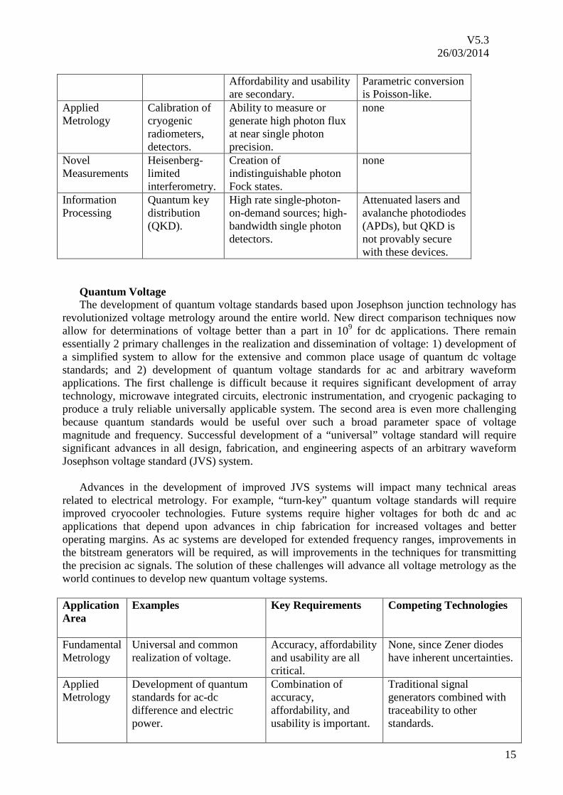
Quantum Voltage The development of quantum voltage standards based upon Josephson junction technology has
revolutionized voltage metrology around the entire world. New direct comparison techniques now allow for determinations of voltage better than a part in 109 for dc applications. There remain essentially 2 primary challenges in the realization and dissemination of voltage: 1) development of a simplified system to allow for the extensive and common place usage of quantum dc voltage standards; and 2) development of quantum voltage standards for ac and arbitrary waveform applications. The first challenge is difficult because it requires significant development of array technology, microwave integrated circuits, electronic instrumentation, and cryogenic packaging to produce a truly reliable universally applicable system. The second area is even more challenging because quantum standards would be useful over such a broad parameter space of voltage magnitude and frequency. Successful development of a “universal” voltage standard will require significant advances in all design, fabrication, and engineering aspects of an arbitrary waveform Josephson voltage standard (JVS) system.
Advances in the development of improved JVS systems will impact many technical areas
related to electrical metrology. For example, “turn-key” quantum voltage standards will require improved cryocooler technologies. Future systems require higher voltages for both dc and ac applications that depend upon advances in chip fabrication for increased voltages and better operating margins. As ac systems are developed for extended frequency ranges, improvements in the bitstream generators will be required, as will improvements in the techniques for transmitting the precision ac signals. The solution of these challenges will advance all voltage metrology as the world continues to develop new quantum voltage systems.
Application Area
Examples Key Requirements Competing Technologies
Fundamental Metrology
Universal and common realization of voltage.
Accuracy, affordability and usability are all critical.
None, since Zener diodes have inherent uncertainties.
Applied Metrology
Development of quantum standards for ac-dc difference and electric power.
Combination of accuracy, affordability, and usability is important.
Traditional signal generators combined with traceability to other standards.
15

V5.3 26/03/2014
Applications as calibrators for oscilloscopes, samplers, and sources.
Electronic Kilogram The goal is to develop a synthesis of mechanical, material, electromagnetic, computational, and
quantum technologies that will become the national kilogram mass standard reference for the foreseeable future. To create a standard reference, all these technologies must be incorporated with absolute traceability to references for the second, meter, volt, and ohm. This traceability, along with stability and reproducibility, must be maintained at better than the part in 108 level in order to accommodate the commercial and scientific needs of the world. With the likely redefinition of the kilogram and assignment of the Planck constant, the volt and ohm will become fixed and independent of the kilogram, but all commerce and scientific measurements related to mass, pressure, and force will be impacted by the electronic kilogram standard.
The challenge is to achieve electronic kilogram systems that can be flawlessly, efficiently, and
continuously operated in several locations around the world. The difficulty in this problem arises in the long-term reproducibility at the high precision required for establishing kilogram that is constant over the next decades. At the part in 108 level, many external environmental effects and internal mechanical or electrical properties are not negligible. Since the resulting standard is an absolute measurement as opposed to a relative measurement, these effects must be characterized (e.g. alignment corrections, gravity acceleration), reduced (e.g. vibrations and radio-frequency interference), or measured such that the effect cancels with the proper experimental procedure (e.g., both the magnitude and drift in the magnetic field, and also heat energy and friction energy losses are eliminated in the dual mode method of the watt balance technique). Some examples of advances needed to make the electronic kilogram a reliable national standard include: a stable magnetic field source less costly in use of liquid helium; more stable, lower noise, and lower leakage electronics and electrical components; laser interferometry electronics that are both fast, very high precision, and accurately timed; and mass standards of materials with surfaces stable under vacuum and mechanical wear.
Application Area
Examples Key Requirements Competing Technologies
Fundamental Metrology
Redefinition of the SI and determination of Planck’s constant.
Accuracy is paramount. Si-sphere Avogadro experiment (still an artifact).
Applied Metrology
Realization of the kilogram. Combination of accuracy, affordability, and usability is important.
Present physical artifacts.
Novel Measurements
Application of the most precise representation of length, time, voltage, resistance, and gravity in an experimental apparatus.
Low uncertainty, repeatability, and reliability are essential.
16

V5.3 26/03/2014
Quantum Computing with Superconducting Qubits Quantum Computing is one of the most exciting and dynamic fields of modern physics with
potential “paradigm shifting” impact in areas as diverse as communication security, digital signatures, computation related to scheduling problems, and simulation of complex systems such as drug synthesis. Numerous implementations of quantum computing are being pursued each using a different physical entity for the quantum bit or qubit. Examples are atoms, ions, isolated spins in solids, and superconducting integrated circuits. The latter approach is particularly challenging, because of the difficulty in isolating the qubit from external perturbations but holds great promise because, once a single long-lived qubit is realized, integration of multiple qubits into complex circuits can be done using well-known techniques from silicon integrated circuits.
To realize a useful qubit one must 1) initialize its quantum state, 2) isolate the qubit sufficiently
from external perturbations such that the quantum state can evolve undisturbed, 3) couple the qubit in a controlled way to neighboring qubits, and finally 4) read out the qubit state with high fidelity. The work addressing each of these needs has profound metrological impact as electrical (and physical) metrology evolves ever more quickly to quantum-based standards and measurements. The sensitivity of a qubit to external perturbations makes it an exquisite detector for other quantum phenomena such as single charge transport and even quantized mechanical motion. The need for isolation has spurred very fundamental research into the role of “quasiparticle poisoning” on the operation of superconducting circuits and the requirement for readout provides impetus for the development of quantum limited high speed amplifiers. Given the profound difficulty of building a quantum computer, it is highly likely that the technology developed pursuing this goal may, in fact, have its first application not in Quantum Information but in quantum-based standards and measurements.
Nano Bioelectronics Research in the biological and medical sciences is evolving from the traditional top-down
observational-based efforts on animal or cell cultures to include methods where measurements of the most fundamental processes enable the understanding of more complex processes. This change has been enabled by the development of new technologies and driven by the need to diagnose and treat disease faster, cheaper, and better for affordable healthcare.
Current optical-based fluorescence methods have high sensitivity for biological and medical
research but instrument miniaturization for portable diagnostics has not yet been achieved. Electronic-based methods have the advantage of enabling portable diagnostic systems but suffer from low sensitivity for measurements of biologically relevant concentrations of analytes. With the advent of microfluidics and nanopore technologies, electronic-based methods can achieve single molecule sensitivity because of the confinement (or packing) of samples into small spaces, which results in measurable concentrations.
A major measurement challenge is to develop measurement methods that can characterize the
response of single cells or small cell populations with single molecule sensitivity, and to do this for multiple analytes. To achieve this, new electronic sensors and methods must be developed. Furthermore, these new methods must be validated with the accepted fluorescence-based methods.
Advances can be applied to a wide variety of technology areas. Nanopore technology can be
used to measure the structure of DNA, but it is not yet clear what detail can be resolved and if DNA can be electronically sequenced. Conductance, pH, and electrochemical sensors can also be developed and integrated amplifiers could also increase sensitivity and performance. Other new
17

V5.3 26/03/2014
technologies include nanowires, single electron devices, and microwave transmission line technology for temperature control and detection.
Application Area
Examples Key Requirements Competing Technologies
Single molecule electronic detection and sequencing
Structure/function measurement of DNA and other stranded molecules: electronic sequencing.
Low current measurement, integration of biological and/or solid-state nanopores in microfludic networks.
Optical fluorescence technologies.
Cellular Biometrology
Drug discovery and approval, determination of cytotoxicity of drugs and toxins.
Ability to control the cellular microenvironment; new electronic sensors; integration of electronics with microfluidics technology.
Robotic-based technologies, optical-based measurement technologies, RNA chips, polymerase chain reaction (PCR), others.
Information Processing
Bio-inspired computing
Methods to extract information stored on DNA.
Semiconductor electronics.
Molecular Electronics The molecule is the single smallest thing that may ever have completely engineered electronic
and optical properties. Therefore, molecular-based electronics, which can be viewed as the ultimate possible miniaturization, is a field that many predict will have important technological impacts on the computational and communication systems of the future. The goal for molecular electronics is to supplement or replace conventional Si-based technologies to extend electronic device performance improvements beyond the incremental scaling of Complementary Metal Oxide Semiconductor (CMOS) devices.
The small size of molecules is the source of their great promise for electronic scaling and
functionalization. However, making reliable, reproducible electrical contacts to sub-lithographic nanoelectronic materials, such as molecules, is a great challenge. Test structures that typically contain ensembles of molecules and characterization techniques are required that enable the intrinsic properties of the molecules to be determined. These measurement methods must separate contact effects and test platform artifacts from the intrinsic molecular conductivity. Physical characterization of the molecules within a molecular electronic device (another metrology challenge) is critical to verify that observed electrical behavior is arising from a change in the molecules in the device. In addition, three-dimensional electromagnetic models incorporating quantum mechanical effects in the device materials are needed to fully understand and interpret measurements of molecular electronic behavior.
While the chemistry of self-assembly enables contact to one side of a properly designed
molecule to be well-controlled and relatively easily formed, making good electrical contact to the other side of molecule is the greatest challenge (and the greatest road-block) to the implementation
18

V5.3 26/03/2014
of a molecular-based electronic technology. This challenge is amplified for single-molecule measurements.
In spite of these challenges, molecular electronics holds great promise as a technology to
improve the performance of information processing technologies beyond the capabilities of the CMOS FET (Field Effect Transistor), the current basis of ULSI (Ultra-Large-Scale Integration) circuits, which is beginning to show fundamental limits associated with the laws of quantum mechanics and the limitations of fabrication techniques.
Application Area
Examples Key Requirements Competing Technologies
Applied Metrology
Self-assembled dielectric film thickness standards
Repeatable self-assembly to form uniform, high-density molecular monolayers.
Atomic layer deposition (ALD), thermal oxidation.
Novel Measurements
Single molecule measurements
Electrical contact to single, isolated molecules. Separation of contact effects from intrinsic behavior.
None.
Novel Measurements
Intrinsic molecular effects
Reliable molecular electronic test structures. Correlation of physical properties with final device performance.
None.
Information Processing
Molecular electronic switches for advanced logic and memory
Electrically active molecules. Uniform, ultra-dense device fabrication. Reliable, long-term performance.
Si-CMOS, other proposed “beyond CMOS” technologies such as spintronics or phase-based circuitry.
Nanoscale microwave metrology and spintronics There is a need to develop fundamental measurement techniques to allow the continued
temporal and spatial scaling of present electronic devices, and to facilitate the development of emergent high-speed nanoelectronic device architectures. Present scaling laws predict that within the next decade the critical dimensions of charge- and spin-based electronic devices will approach only a few tens of nanometers and will operate at gigahertz frequencies. Few measurements have been performed in this regime. Furthermore, below 5 nm dimensions, CMOS devices are not expected to function reliably, and alternative device architectures, such as nanotube FETs and spintronic devices, are being explored as potential replacements.
While significant progress has been made in gaining a rudimentary understanding of these
devices, it has largely been confined to low-frequency and dc operation. Presently, there is a lack of understanding of how such systems behave and couple to one another at frequencies from 100 MHz to above 100 GHz. In order for their potential to be realized, measurements methods in the gigahertz regime must be developed and understood. Such measurements are a “big” problem because: (1) the standard measurement techniques implemented at low frequencies cannot be applied or extrapolated to the microwave regime; (2) combining high spatial resolution with high
19
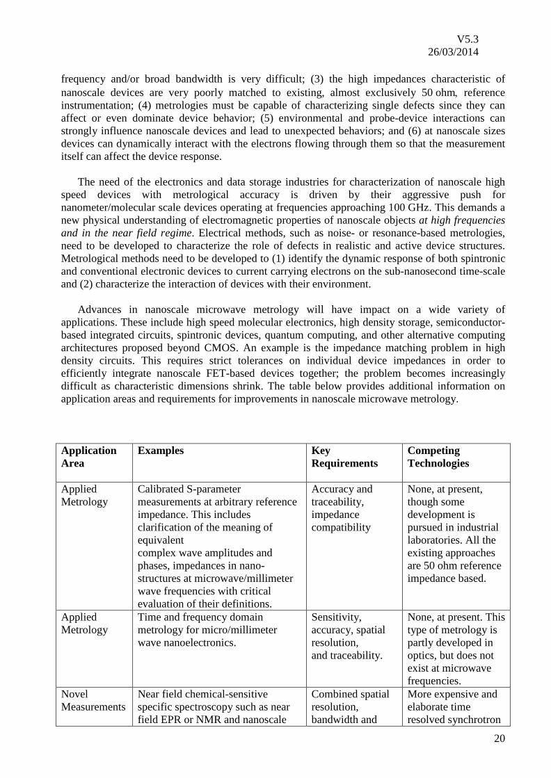
V5.3 26/03/2014
frequency and/or broad bandwidth is very difficult; (3) the high impedances characteristic of nanoscale devices are very poorly matched to existing, almost exclusively 50 ohm, reference instrumentation; (4) metrologies must be capable of characterizing single defects since they can affect or even dominate device behavior; (5) environmental and probe-device interactions can strongly influence nanoscale devices and lead to unexpected behaviors; and (6) at nanoscale sizes devices can dynamically interact with the electrons flowing through them so that the measurement itself can affect the device response.
The need of the electronics and data storage industries for characterization of nanoscale high
speed devices with metrological accuracy is driven by their aggressive push for nanometer/molecular scale devices operating at frequencies approaching 100 GHz. This demands a new physical understanding of electromagnetic properties of nanoscale objects at high frequencies and in the near field regime. Electrical methods, such as noise- or resonance-based metrologies, need to be developed to characterize the role of defects in realistic and active device structures. Metrological methods need to be developed to (1) identify the dynamic response of both spintronic and conventional electronic devices to current carrying electrons on the sub-nanosecond time-scale and (2) characterize the interaction of devices with their environment.
Advances in nanoscale microwave metrology will have impact on a wide variety of
applications. These include high speed molecular electronics, high density storage, semiconductor-based integrated circuits, spintronic devices, quantum computing, and other alternative computing architectures proposed beyond CMOS. An example is the impedance matching problem in high density circuits. This requires strict tolerances on individual device impedances in order to efficiently integrate nanoscale FET-based devices together; the problem becomes increasingly difficult as characteristic dimensions shrink. The table below provides additional information on application areas and requirements for improvements in nanoscale microwave metrology.
Application Area
Examples Key Requirements
Competing Technologies
Applied Metrology
Calibrated S-parameter measurements at arbitrary reference impedance. This includes clarification of the meaning of equivalent complex wave amplitudes and phases, impedances in nano-structures at microwave/millimeter wave frequencies with critical evaluation of their definitions.
Accuracy and traceability, impedance compatibility
None, at present, though some development is pursued in industrial laboratories. All the existing approaches are 50 ohm reference impedance based.
Applied Metrology
Time and frequency domain metrology for micro/millimeter wave nanoelectronics.
Sensitivity, accuracy, spatial resolution, and traceability.
None, at present. This type of metrology is partly developed in optics, but does not exist at microwave frequencies.
Novel Measurements
Near field chemical-sensitive specific spectroscopy such as near field EPR or NMR and nanoscale
Combined spatial resolution, bandwidth and
More expensive and elaborate time resolved synchrotron
20

V5.3 26/03/2014
material characterization. High resolution spectroscopy of magnetic nanostructures, characterization of charge-based single-photon sources, particle detectors, electromagnetic field mapping, etc. Device control with electron spin.
chemical sensitivity.
and x- ray approaches
Information Processing
Active spintronic devices, nanoscale microwave sources and spectral analysis, magnetic random access memory, hard disk drives.
Improvements upon CMOS, microwave power output, ultra-high speed behavior, nanoscale spectroscopy.
Quantum computing, MEMS/NEMS, optical processing.
Nanomagnetism Nanomagnetic structures and devices are penetrating various sectors of today´s society ranging
from information and communication technology to health care. While a sound metrological basis including standards and traceability chains has been established for measuring the magnetic properties of macroscopic objects, metrology for nanomagnetism is still in its infancy. Outlined below are “big problems” of nanomagnetism, among them some that are common to nanotechnology in general (e.g., refer to the section above on nanoscale microwave metrology).
While traceable measurement techniques for the magnetic field and the magnetization have
limited spatial resolution, high-resolution microscopy techniques are lacking traceability (e.g., Lorentz microscopy, magnetic force microscopy, spin polarized scanning tunneling microscopy). Thus, efforts are required to trace back nanoscale measurements to the existing macroscopic standards. Along with this effort, the sensitivity and spatial resolution of magnetic field probes like nano-SQUID and nano-Hall sensors need to be increased. In some cases, the invasiveness of the measurements process, i.e., the change of the measured object in response to the probe, has also to be addressed.
Nanomagnetic structures often exhibit ultrafast dynamic behavior with bandwidths in the GHz
range and beyond. The large bandwidth is inherently linked to their small size, e.g., GHz precessional dynamics is based on a macrospin approximation, which is only valid for single-domain structures. Traceable methods for the measurement of ultrafast magnetization switching need to be developed along with standards for high-frequency test beds for ultrafast measurements (coplanar waveguides, microstrip lines).
Research in nanomagnetism has led to the discovery of qualitatively new device concepts and
devices such as, e.g., spin-torque memory cells and spin-torque oscillators, for which metrology is required. This development together with the effort to merge magnetism with semiconductor technology in the field of semiconductor spintronics has drawn the attention to physical quantities that were less important in magnetic metrology in the past. This includes, e.g., the degree of spin polarization of spin polarized currents or the efficiency of spin injection over an interface between different materials. Providing a sound metrological basis for the measurement of these quantities presents a considerable challenge.
21

V5.3 26/03/2014
Meeting the challenges outlined above will impact key information and communication technologies like high-density data storage or non-volatile computers memories. In medicine and life science solving the big problems of nanomagnetic metrology will bring substantial benefits to all technologies that rely on magnetic nanoparticles.
SI Traceable High-Frequency Electromagnetic Field Measurements Ideally, radio-frequency (audio to optical) electromagnetic field measurements (electric field in
V/m and magnetic field in A/m) would be directly linked to SI units with low intrusion, fast response, wide dynamic range (mV/m to kV/m and μA/m to A/m) and low uncertainty (less than 0.1 dB or less than 1%). The current state-of-the art is far short of this goal. At present, radio-frequency electromagnetic field measurements typically assume far-field conditions, measure the electric field only, use a small dipole with a diode based voltage detector, are only indirectly linked to the SI units, cannot accurately detect fields below 1 V/m, and have uncertainties on the order of 0.5 dB or greater than 5%. Presently used electromagnetic field probes were developed some 20 years ago and could be improved based on advances in materials and electronics. However, to achieve an order of magnitude improvement (or several orders) a new physical approach to electromagnetic field measurements is needed. No NMI has been able to improve on the diode probes to date. A true breakthrough improvement remains a difficult EM problem.
Optical modulators are a low intrusion alternative to dipoles; however, they cannot currently
achieve significant sensitivity or accuracy gains. Electromagnetic field probes based on Rabi oscillations could potentially achieve high sensitivity and low uncertainty, but no obvious way to go from this atomic scale effect to a usable field probe presently exists. The Stark effect couples field strength with line spectra of a gas and may present a possible approach; however, again it is not clear how to go from this quantum effect to a usable field probe.
Development of a more robust foundation for electromagnetic field measurements is extremely
unlikely except with the focused attention of the NMI community. Improved electromagnetic field probes would improve traceability worldwide and would also benefit high performance electromagnetic systems, such as radar, satellite, radiometer, and communication systems. Higher sensitivity and higher accuracy sensors and instrumentation would also enable new applications in electromagnetic imaging, in particular biomedical applications.
Quantized resistances of QHR arrays, newly fabricated materials, and related CCC
technique. Since 1990, a single bar QHR (Quantized Hall Resistance) is adopted as a primary standard of
DC resistance. Quantized Hall Array Resistance Standards (QHARS) have been studied extensively and in the future they could be working standards if the technique for the fabrication process of the arrays is finalized. And hopefully QHARS could be recognized as a primary standard after sufficient evaluation. Crystal growth of GaAs/AlGaAs heterostructures has been well developed, high quality substrates are utilized for many applications. The newest techniques of fabrication of high quality ohmic contacts and insulation layers could be applied to the integration of QHR bars. High quality substrates could reduce the required magnetic fields. Arrays of value 100 Ω or 10 kΩ could be very useful for traveling standards first of all, and as working standards in many NMIs.
Recently various new heterostructure materials have been fabricated with the state-of-the-art
combinatorial method, and surveyed for various purposes and in some cases in quest of a high-mobility electron gas. For example, in ZnO/MgxZn1-xO heterostructures Shubnikov-de Haas
22
V5.3 26/03/2014
oscillation and quantized Hall resistance were reported. And a LaAlO3/SrTiO3 heterostructure was confirmed to have very high mobility and showed Shubnikov-de Haas oscillation. It is important to monitor the material fabrication research in that field, and, if necessary, we have to evaluate such materials from the metrology point of view.
In March 2007, graphene (single layer graphite) was reported to show quantized Hall resistance
at 300 K. Electrically or chemically doped carriers of graphene have sub-micrometer-scale ballistic transport properties. And it also acts as weak link between superconducting electrodes and demonstrates the Josephson effect. It is reported that nanometer ribbons and quantum dot structures carved in graphene have a SET-like behavior. This incredible material could be a candidate to replace current GaAs/AlGaAs heterostructure-based QHR standard devices. Because its Landau levels split largely with several hundred to several thousand kelvins, we might have a possibility to operate the QHR at an elevated temperature and/or at lower magnetic field. The universality of the quantum Hall effect of graphene in comparison with that of a GaAs/AlGaAs heterostructure has been confirmed recently. If in addition to this the operation in moderate conditions will become possible after enough evaluation, a QHR system might be utilized at various laboratories, not only at expert NMIs.
It is believed that the electronics of CCC is well matured. But CCC cores are still handcrafted.
If it would be possible to fabricate such CCC cores in a superconducting process, as it is widely utilized in Josephson junction fabrication technique (i.e. Nb-Al process), CCCs could then be cooled by compact liquid helium-free cryostats. In this case, CCC bridges could be utilized in many NMIs and replace conventional DCCs in some cases. For this purpose, the thickness and quality of the Nb and insulation layers are important.
Traceable THz Metrology Terahertz (THz) technology is a rapidly growing field with a wide range of exciting early
applications that take advantage of unique material properties at these frequencies. Applications include medical imaging systems, spectroscopy of molecular and biological systems, remote sensing and standoff detection for homeland security, atmospheric monitoring for pollutants and climate change science and cosmic microwave background (CMB) measurement to research the origin of the Universe and the physical laws governing the Universe. All of these efforts are for the development of components or measurement systems aimed at specific applications, with no concerted effort to address the underlying metrology infrastructure. NMIs will be needed to develop and deliver the essential measurement techniques and standards required to provide reliable and robust traceability for key measurement parameters in the terahertz frequency range. At present the THz community attempts to meet its metrology needs in an ad hoc fashion, generally using microwave or IR components far beyond their specified frequency range, even though basic physics considerations suggest they would be inaccurate. Microwave measurements currently reach up to ~100 GHz, while IR techniques extend to below ~10 THz. For the THz frequencies in between, this has left even the most basic of metrological tools, such as power meters, with serious gaps in capabilities over the needed power and frequency ranges, and without traceability. Immediate critical needs of the THz community are calibrated power measurements and the instrumentation and techniques to make quantifiable THz measurements of material properties and the interactions between THz radiation and measurement systems. As for CMB measurement it is believed since recently that the information of CMB polarization, which is measured by superconducting detectors, will play an important role to disclose the true figure of the Universe in the time shortly before the Big Bang. Quick and accurate calibration technique for such detectors will contribute to this scientific activity.
23

V5.3 26/03/2014
High-speed Communications and associated metrology The NMIs must continue to develop next generation measurement methods and services for
high-speed waveform measurements and other metrologies to support advanced high-speed communications. Such measurements include traceable measurements of ultra-fast pulses, combining time and frequency domain techniques, as well as new systems level measurements for both optical and wireless. For example, to economically meet growing demand for capacity, networks must optimize use of infrastructure and spectrum. This requires more efficient use of bandwidth and extensive reconfigurability of network elements, including routing of paths and channels. These advances require development of completely new paradigms to support physical layer measurements for both fiber optic and wireless systems. The measurement needs for next-generation networks far exceed today’s capabilities and demand a multidisciplinary approach that accurately quantifies the physical-layer performance of frequency-, waveform-, and path-agile networks.
Physiological effects of ac and dc magnetic fields The highest magnetic fields to which the human body is normally exposed occur during
magnetic resonance imaging (MRI). Clinical MRI systems create static magnetic flux densities of typically 1.5 to 3 T and smaller superimposed radio frequency (RF) fields.
Regulations exist or are in preparation to limit the exposure to the risks arising from
electromagnetic fields. These risks include effects on nervous system functions in the body, and the recent EU Directive 2004/40/EC defines exposure limits for workers in the frequency range from 1 Hz to 10 MHz with respect to the induced maximum current densities in the human body. The link between these induced current densities and the related, more directly accessible electric and magnetic field strengths is based on numerical modelling, but no experimental verification exists. Also, the knowledge of physiological reference data, as for example tissue conductivities in the human body, is very limited. Motion of workers in the stray field of MRI scanners or other large dc magnets also leads to induced currents, which can become significantly large. At present, these current densities are determined by numerical modelling but also in this case no experimental verification exists.
A possible field of contribution of metrology would be the measurement of physiological
properties needed as input for the calculations. It might also be useful that the CCEM or NMIs active in this field establish contact with ICNIRP, the International Commission on Non-Ionizing Radiation Protection, which is recognized by the WHO, ILO and other bodies as the international independent advisory body for this field.
Other specific technical metrology challenges Communication with nanosystems (acoustical, optical, electromagnetic, nano-micro interface) Nanomeasurements (CNT properties) Fermi surface measurement Societal, Economic, and Cross-cutting Areas
24

V5.3 26/03/2014
Energy Smart Grid (intelligent electric grid) Transformer and other power equipment efficiency
Fuel cell Solar
Environment Climate change Detectors for monitoring
Health Bioelectronic (mentioned above) Toxicity Electronic Implants Imaging EMF effects (cellular telephones) Homeland Security Challenges facing the NMIs and RMOs Interactions with national SDOs, international standards bodies, and accreditation bodies.
Efficiently and effectively supporting the CIPM MRA with a well-designed key comparison process using stable and appropriate transfer.
Mutual agreement among regional NMIs which would enable the termination of some services
offered elsewhere in the region.
25