catalogue spring 2018 xilinx-based products - … · catalogue spring 2018 mercury+ xu1....
TRANSCRIPT

Catalogue Spring 2018
Mercury+ XU1. Unprecedented CPU performance, with Zynq® UltraScale+™.
Xilinx-based Products
Everything FPGA.
Everything FPGA.
At Enclustra, everything is FPGA.
Our products are used by more than a thousand customers in more than 50 countries worldwide, and our customer base is still growing quickly. But we don’t just stick to hardware and IP – we do customer design projects too; every stage of development, from conception through to bring-up at the customer site. We have 14 years of FPGA system design under our belt; break it down a little further and our team of engineers has far in excess of 200 person years of FPGA experience.
That experience and expertise enables us to create the best experience for our customers: we pride ourselves on the quickest, highest possible quality of service and delivery from the moment you get in touch, to the moment your system starts up in the field for the first time.
As with our product range and our customer base, our list of completed projects is growing – to keep up with developments, and not miss any of our upcoming innovations, subscribe to our newsletter at www.enclustra.com/subscribe
This catalogue presents our current product and service range; if anything piques your interest, don’t hesitate to get in touch.
Thanks and happy reading!
The Enclustra Team.

» Contents
Hardware Products Our Hardware Products 4
Modules Module Overview 5
Mercury+ XU1 6
Mercury XU5 7
Mercury+ XU6 8
Mercury XU7 9
Mercury ZX1 10
Mercury ZX5 11
Mercury KX1 12
Mercury+ KX2 13
Mars XU3 14
Mars ZX2 15
Mars ZX3 16
Mars AX3 17
Selection Guides Mars FPGA Modules Selection Guide 18
Mercury FPGA Modules Selection Guide 22
Mercury SoC Modules Selection Guide 24
Base Boards & Other Mercury+ PE1 32
Mercury+ PE3 33
Mars EB1 34
Mars PM3 35
FMC DR2 36
Cosmos XZQ10 37
Tools & Design Support Linux Build Environment 38
Module Configuration Toolkit 39
Design Support 40
IP Solutions Our IP Solutions 41
Universal Drive Controller 42
FPGA Manager 44
Stream Buffer Controller 46
Display Controller 47
UDP/IP Ethernet 48
Further Information 49

4FPGA DESIGN Center
Enclustra hardwareDelivered fast; made to last
Our modules all come with a minimum expected lifetime of 10+ years; seeing as we also design our hardware with forward-looking availability and performance in mind, this means you can depend on our products to deliver over the long term.
Our modules are also largely pin-compatible within their module family, meaning you can also plan a clear upgrade path. A full selection guide and roadmap can be found after the individual module info pages.
In the case that you wish to manufacture our products by yourself, we also offer a hardware production licence. Get in touch for more details.

5FPGA DESIGN Center
Mars Form FactorA family of modules in the compact and popular SO-DIMM form factor.
Mercury Form FactorA family of modules optimized for demanding, high-bandwidth applications.
Mercury+ Form FactorThe raw computing power of the Mercury family, with an even higher I/O count.
» Module Overview
Module FPGA/SoC Device User I/Os System Logic Cells
Mars AX3 Artix-7 108 Up to 101k
Mars MX1 Spartan-6 108 44k
Mars MX2 Spartan-6 LX 108 44k
Mars XU3 Zynq UltraScale+ 108 Up to 154k
Mars ZX2/ZX3 Zynq-7000 108 Up to 85k
Module FPGA/SoC Device User I/Os System Logic Cells
Mercury KX1 Kintex-7 178 Up to 407k
Mercury XU5 Zynq UltraScale+ 178 Up to 256k
Mercury XU7 Zynq UltraScale+ 178 Up to 747k
Mercury ZX1 Zynq-7000 Up to 178 Up to 350k
Mercury ZX5 Zynq-7000 178 Up to 125k
Module FPGA/SoC Device User I/Os System Logic Cells
Mercury+ KX2 Kintex-7 256 Up to 407k
Mercury+ XU1 Zynq UltraScale+ 294 Up to 747k
Mercury+ XU6 Zynq UltraScale+ 270 Up to 256k

OS support:
� Xilinx® Zynq UltraScale+ MPSoC� Quad-core ARM® Cortex™-A53� Dual-core ARM Cortex-R5� Up to 8 GB DDR4 SDRAM� 64 MB QSPI flash� 16 GB eMMC flash� PCIe® Gen2 ×4� 16 × 6/12.5/15 Gbps MGT� 2 × Gigabit Ethernet� 2 × USB 2.0/3.0� Up to 747,000 system logic cells� 294 user I/Os� 5–15 V supply� 74 × 54 mm
4 MGTs (PCIe Gen2 ×4)
4 MGTs 72 I/Os (1.8V)
72-bit
8-bit
I2C | JTAG | Configuration
1.8V3.3V
5-15V
2.5V
PS | PL
14 I/Os(3.3V)
52 I/Os(3.3V)
76 I/Os (1.8V)
8 MGTs
PLPS PL
PS
PS
PS
PS
PL
PL
PSPL
UltraSCALE+ZYNQ ®
168-pin Hirose FX10 Connector
168-pin Hirose FX10 Connector
Mercury+ XU1
Quad SPI Flash
eMMC Flash
DDR4ECC
SDRAM
Gigabit Ethernet PHY (x2)
168-
pin
Hiro
se F
X10
Conn
ecto
r
USB 2.0/3.0 PHY (x2)
Power Supply
6
MERCURY+ XU1Zynq® UltraScale+™ SoC Module
ME-XU1-6EG-1I-D11E
1+ €904
100+ €798
10000+ €588
Mercury+ PE1 Kit €1318
ME-XU1-15EG-2I-D12E
1+ €1601
100+ €1415
10000+ €1071
Mercury+ PE1 Kit €2015

MERCURY XU5Zynq® UltraScale+™ SoC Module
� Xilinx® Zynq UltraScale+ MPSoC� Quad-core ARM® Cortex™-A53� Dual-core ARM Cortex-R5� H.264 / H.265 Video Codec � Up to 8 GB DDR4 SDRAM� 16 GB eMMC flash� 64 MB QSPI flash� PCIe® Gen3 ×4, PCIe® Gen2 ×4� 8 × 6/12.5/15 Gbps MGT� 2 × Gigabit Ethernet� 2 × USB 2.0/3.0� Up to 256,000 system logic cells� 178 user I/Os� 5–15 V supply� 56 × 54 mm
In development – please contact us for availability.
ME-XU5-2EG-1I-D11E
1+ €319
100+ €279
10000+ €201
Mercury PE1 Kit €603
ME-XU5-5EV-2I-D12E
1+ €784
100+ €691
10000+ €511
Mercury PE1 Kit €1068OS support:
72-bitPS | PL
DDR4 ECC
SDRAMUltraSCALE+
ZYNQ ®
4 MGTs (PCIe Gen2 ×4)
4 MGTs (PCIe Gen3 ×4)or 20 I/Os (1.8V)
72 I/Os (1.8V)
1.8V3.3V2.5V
I2C | JTAG | Configuration
14 I/Os(3.3V)
5-15V 52 I/Os(3.3V)
PL
PL PLPS
PS
PS
PSPL
Mercury XU5
Quad SPI Flash
168-pin Hirose FX10 Connector
168-pin Hirose FX10 Connector
Gigabit Ethernet
PHY
Gigabit Ethernet
PHY
USB 2.0/3.0 PHY (x2)
8-bit
Power Supply
eMMC Flash
16-bitPLDDR4 SDRAM
PS
7

� Xilinx® Zynq UltraScale+ MPSoC� Quad-core ARM® Cortex™-A53� Dual-core ARM Cortex-R5� Up to 8 GB DDR4 ECC SDRAM� 16 GB eMMC flash� PCIe® Gen3 ×4� Up to 8 × 6/12.5 Gbps MGT� 2 × Gigabit Ethernet, USB 2.0/3.0� Up to 256,000 system logic cells� 270 user I/Os� 5–15 V supply� 74 × 54 mm
MERCURY+ XU6Zynq® UltraScale+™ SoC Module
ME-XU6-2EG-1I-D11E
1+ €391
100+ €343
10000+ €228
Mercury+ PE1 Kit €805
ME-XU6-5EV-2I-D12E
1+ €853
100+ €753
10000+ €537
Mercury+ PE1 Kit €1267
Preliminary product information – please contact us for availability.
OS support:
UltraSCALE+ZYNQ ®
4 MGTs (PCIe Gen2 ×4)
4 MGTs 72 I/Os (1.8V)
72-bit
48 I/Os (1.8V)
44 I/Os (3.3V)
I2C | JTAG | Configuration
1.8V3.3V
5-15V
2.5V
PS | PL
14 I/Os(3.3V)
52 I/Os(3.3V)
PLPL
PL
PL
PSPL
PS
PS
PS
PL
168-pin Hirose FX10 Connector
168-pin Hirose FX10 Connector
Mercury+ XU6
Quad SPI Flash
eMMC Flash
Cypress FX3 USB 3.0
DDR4ECC
SDRAM
Gigabit Ethernet PHY (x2)
168-
pin
Hiro
se F
X10
Conn
ecto
r
USB 2. PHY (x2)
Power Supply
8

OS support:
� Xilinx® Zynq UltraScale+ MPSoC� Quad-core ARM® Cortex™-A53� Dual-core ARM Cortex-R5� Up to 8 GB DDR4 ECC SDRAM� 16 GB eMMC flash� 64 MB QSPI flash� PCIe® Gen3 ×4� Up to 12 × 6/12.5/15 Gbps MGT� 2 × Gigabit Ethernet� USB 2.0/3.0� Up to 747,000 system logic cells� 178 user I/Os� 5–15 V supply� 74 × 54 mm
Preliminary product information – please contact us for availability.
MERCURY XU7Zynq® UltraScale+™ SoC Module
ME-XU7-6EG-1I-D11E
1+ €954
100+ €824
10000+ €600
Mercury PE1 Kit €1238
ME-XU7-15EG-2I-D12E
1+ €1667
100+ €1456
10000+ €1096
Mercury PE1 Kit €1951
UltraSCALE+ZYNQ ®
8 MGTs48 I/Os 4 MGTs (PCIe Gen3 ×4)
4 MGTs (PCIe Gen2 ×4)
32-bit
8-bit
1.8V3.3V2.5V
I2C | JTAG | Configuration
14 I/Os5-15V 52 I/Os
PS | PL
72-bit
PL
PS
PS
PS
PS
PL PS
PL
PL
PL
168-pin Hirose FX10 Connector
168-pin Hirose FX10 Connector
Mercury XU7
eMMC Flash
DDR4 SDRAM
USB 2.0 PHY
Quad SPI Flash
DDR4 ECC SDRAM
Gigabit Ethernet PHY (x2)
Power Supply
9

� Xilinx® Zynq-7030/7035/7045 SoC FPGA� Dual-core ARM® Cortex™-A9� 1 GB + 256 MB DDR3L SDRAM� 64 MB QSPI flash� 512 MB NAND flash� PCIe® Gen2 ×4/×8� Up to 8 × 6.6/10.3125 Gbps MGT� Gigabit Ethernet� 2 × Fast Ethernet� USB 2.0 OTG� Up to 350,000 system logic cells� Up to 178 user I/Os� 5–15 V supply� 64 × 54 mm
OS support:
ZYNQ ®
PS | PL
PS | PL
8/4 MGTs (PCIe Gen2 ×8/×4)
32-bit
16-bit
1.8V3.3V2.5V
I2C | JTAG | Configuration
66 I/Os(3.3V)5-15V
PL
PS
PS
PL
PL
84/72 I/Os(1.8V)
PL
PS
168-pin Hirose FX10 Connector
168-pin Hirose FX10 Connector
Mercury ZX1
NAND Flash
USB 2.0 PHY
Fast Ethernet PHY (x2)
Gigabit Ethernet PHY
200 MHz SDRAM
33 MHz SDRAM
DDR3 SDRAM
DDR3 SDRAM
Real-time Clock
Quad SPI FlashPower Supply
10
MERCURY ZX1Zynq®-7030/7035/7045 SoC Module
ME-ZX1-30-2I-D10
1+ €429
100+ €359
10000+ €226
Mercury PE1 Kit €713
ME-ZX1-45-2I-D10-P
1+ €995
100+ €819
10000+ €496
Mercury PE1 Kit €1279

OS support:
� Xilinx® Zynq-7015/7030 SoC FPGA� Dual-core ARM® Cortex™-A9� 1 GB DDR3L SDRAM� 64 MB QSPI flash� 512 MB NAND flash� PCIe® Gen2 ×4� 4 × 6.25/6.6 Gbps MGT� Gigabit Ethernet� USB 2.0 OTG� Up to 125,000 system logic cells� 178 user I/Os� 5–15 V supply� 56 × 54 mm
MERCURY ZX5Zynq®-7015/7030 SoC Module
ME-ZX5-15-2I-D10
1+ €275
100+ €256
10000+ €157
Mercury PE1 Kit €559
ME-ZX5-30-1I-D10
1+ €323
100+ €290
10000+ €184
Mercury PE1 Kit €607
UltraSCALE+ZYNQ ®
PS | PL
4 MGTs (PCIe Gen2 ×4)
92 I/Os (1.8V/3.3V)
32-bit
1.8V3.3V2.5V
I2C | JTAG | Configuration
12 I/Os(3.3V)
5-15V 54 I/Os(3.3V)
PS
PSPL
PL PS
PS
PS
168-pin Hirose FX10 Connector
168-pin Hirose FX10 Connector
Mercury ZX5
NAND FlashReal-time Clock
USB 2.0 PHY33 MHz Clock
Quad SPI Flash
DDR3L SDRAM
Gigabit Ethernet
PHY
Power Supply
11
5-15V
4 MGTs (PCIe Gen2 ×4)
92 I/Os (3.3V)
32-bit
1.8V3.3V2.5V
8-bit
I2C | JTAG | Configuration
66 I/Os(3.3V)
32-bit
KINTEX ®7
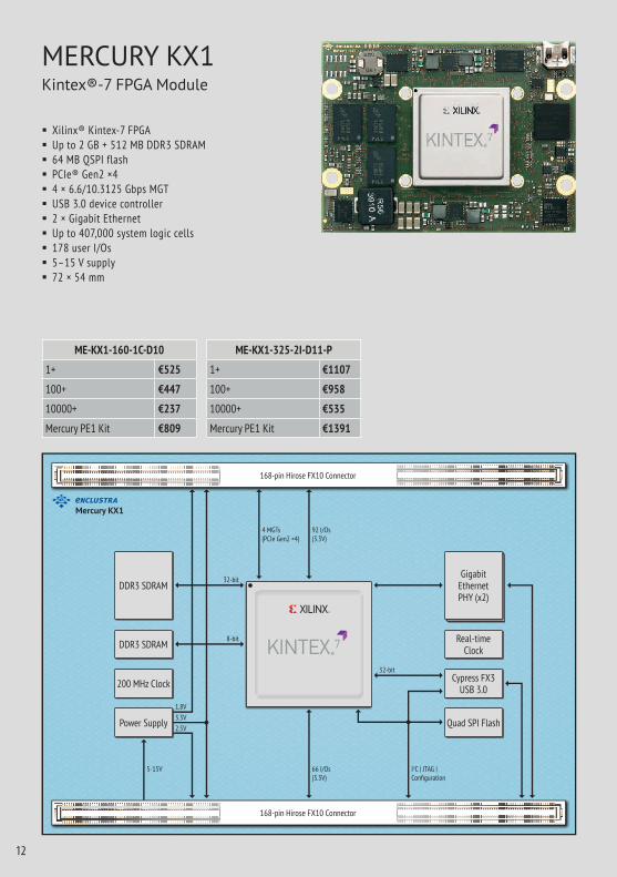
Mercury KX1
Power Supply
200 MHz Clock Cypress FX3 USB 3.0
DDR3 SDRAM Real-time Clock
Quad SPI Flash
DDR3 SDRAMGigabit
Ethernet PHY (x2)
168-pin Hirose FX10 Connector
168-pin Hirose FX10 Connector
12
MERCURY KX1Kintex®-7 FPGA Module
� Xilinx® Kintex-7 FPGA� Up to 2 GB + 512 MB DDR3 SDRAM� 64 MB QSPI flash� PCIe® Gen2 ×4� 4 × 6.6/10.3125 Gbps MGT� USB 3.0 device controller� 2 × Gigabit Ethernet� Up to 407,000 system logic cells� 178 user I/Os� 5–15 V supply� 72 × 54 mm
ME-KX1-160-1C-D10
1+ €525
100+ €447
10000+ €237
Mercury PE1 Kit €809
ME-KX1-325-2I-D11-P
1+ €1107
100+ €958
10000+ €535
Mercury PE1 Kit €1391

� Xilinx® Kintex-7 FPGA� Up to 4 GB DDR3L SDRAM� 64 MB QSPI flash� PCIe® Gen2 ×8� 8 × 6.6/10.3125 Gbps MGT� USB 2.0 device controller� 2 × Gigabit Ethernet� Up to 407,000 system logic cells� 256 user I/Os� 5-15 V single supply� 74 × 54 mm
MERCURY+ KX2Kintex®-7 FPGA Module
ME-KX2-160-2I-D11-P
1+ €581
100+ €492
10000+ €296
Mercury+ PE1 Kit €995
ME-KX2-325-2I-D11-P
1+ €1196
100+ €945
10000+ €513
Mercury+ PE1 Kit €1610
8 MGTs (PCIe Gen2 ×8)
72 I/Os(3.3V)
64-bit
8-bit
I2C | JTAG | Configuration
66 I/Os(3.3V)
1.8V3.3V
5-15V
2.5V
78 I/Os (3.3V)
KINTEX ®7
168-pin Hirose FX10 Connector
168-pin Hirose FX10 Connector
Mercury+ KX2
FTDI USB 2.0
Quad SPI Flash
200 MHz Clock
DDR3 SDRAM
Gigabit Ethernet PHY (x2)
168-
pin
Hiro
se F
X10
Conn
ecto
r
Power Supply
13

OS support:
MARS XU3Zynq® UltraScale+™ SoC Module
� Xilinx® Zynq UltraScale+ MPSoC� Quad/dual-core ARM® Cortex™-A53� Dual-core ARM Cortex-R5� Up to 4 GB DDR4 SDRAM� 16 GB eMMC flash� 64 MB QSPI flash� PCIe® Gen2 ×4� 4 × 6 Gbps MGT� Gigabit Ethernet� USB 3.0� USB 2.0 OTG� Up to 154,000 system logic cells� 108 user I/Os� 67.6 × 30 mm SO-DIMM
MA-XU3-2CG-1E-D10
1+ €196
100+ €173
10000+ €126
Mars EB1 Kit €425
MA-XU3-3EG-2I-D11
1+ €367
100+ €326
10000+ €233
Mars EB1 Kit €596
14
PS | PL
3.3V 1.8V
32-bit
4 MGTs (PCIe Gen2 ×4)
8-bit
24 I/Os (3.3V)
52 I/Os (1.8V)
12 I/Os (3.3V)
I2C | JTAG | Configuration
PS
PS
PL PL PS
PS
PS
UltraSCALE+ZYNQ ®
Gigabit Ethernet
PHYDDR4 SDRAM
Quad SPI Flash
USB 2.0/3.0 PHY
eMMC Flash
Mars XU3
Power Supply

OS support:
MA-ZX2-10-2I-D9
1+ €135
100+ €118
10000+ €83
Mars EB1 Kit €383
MA-ZX2-20-2I-D9
1+ €169
100+ €148
10000+ €106
Mars EB1 Kit €417
MARS ZX2Zynq®-7010/7020 SoC Module
� Xilinx® Zynq-7010/7020 SoC FPGA� Dual-core ARM® Cortex™-A9� Up to 1 GB DDR3L SDRAM� 64 MB QSPI flash� USB 2.0 OTG� Gigabit Ethernet� Up to 85,000 system logic cells� 108 user I/Os� 3.3 V single supply� 67.6 × 30 mm SO-DIMM
15
ZYNQ ®PS | PL
I2C | JTAG | Configuration
3.3V 1.8V
16-bit
96 I/Os (3.3V)
12 I/Os (3.3V)
PS
PS
PL PS
Gigabit Ethernet
PHY
4 LEDs
33 MHz Clock
Real-time Clock
Quad SPI Flash
USB 2.0 PHY
DDR3L SDRAM
Mars ZX2
Power Supply

OS support:
16
MARS ZX3Zynq®-7020 SoC Module
� Xilinx® Zynq-7020 SoC FPGA� Dual-core ARM® Cortex™-A9� Up to 1 GB DDR3L SDRAM� 64 MB QSPI flash� 512 MB NAND flash� USB 2.0 OTG� Gigabit Ethernet� Up to 85,000 system logic cells� 108 user I/Os� 3.3 V single supply� 67.6 × 30 mm SO-DIMM
MA-ZX3-20-1C-D9
1+ €201
100+ €177
10000+ €102
Mars EB1 Kit €430
MA-ZX3-20-2I-D10
1+ €257
100+ €225
10000+ €132
Mars EB1 Kit €505
ZYNQ ®
PS | PL
32-bit PS | PL
I2C | JTAG | Configuration
3.3V 1.8V 108 I/Os (3.3V)
PS
PS
PL
4 LEDs
50 MHz Clock
Real-time Clock
Gigabit Ethernet
PHY
Quad SPI Flash
NAND Flash
DDR3 SDRAM
USB 2.0 PHY
Mars ZX3
Power Supply

MA-AX3-35-1I-D8
1+ €128
100+ €118
10000+ €78
Mars PM3 Kit €387
MA-AX3-100-2I-D8
1+ €242
100+ €208
10000+ €133
Mars PM3 Kit €501
MARS AX3Artix®-7 FPGA Module
� Xilinx® Artix-7 FPGA� Up to 512 MB DDR3L SDRAM� 64 MB QSPI flash� Gigabit Ethernet� Up to 101,440 system logic cells� 108 user I/Os� 3.3 V single supply� 67.6 × 30 mm SO-DIMM
17
ARTIX ®7
3.3V 1.8V
16-bit
I2C | JTAG | Configuration
108 I/Os (3.3V)
Gigabit Ethernet
PHY
4 LEDs
50 MHz Clock
Quad SPI Flash
DDR3 SDRAM
Mars AX3
Power Supply

18
Mars FPGA Modules Selection Guide
Valid as of 26th February 2018
FPGA Family
FPGA Device Name
FPGA Speed Grade*2
FPGA Part Number*2
CPU Cores
CPU Frequency @ MHz
PS Cores & Peripherals
PS Ethernet | USB
PS SDRAM Size (MByte)
PS SDRAM Type | Bandwidth (MByte/s)
PL System Logic Elements
PL Block RAM (kbit)
PL DSP Systolic FIR (MMAC/s)
PL MGT Transceivers @ Gbps*6
PL Peripherals
PL Ethernet | USB*5
PL SDRAM Size (MByte)
PL SDRAM Type | Bandwidth (MByte/s)
Flash Memory
Connector Pins | IO Pins
PL 3.3V | PL 1.8V Pins | PS Pins
Module Dimensions (mm)
Temperature Range*2
Boot Modes
Product Status
Estimated Product Lifetime*3
Preferred Configuration | MOQ*4
Module Order Code
Budgetary Price 1+ (EUR)
Budgetary Price 30+ (EUR)
Budgetary Price 100+ (EUR)
Budgetary Price 1000+ (EUR)
Budgetary Price 10000+ (EUR)
Mars™ ZX2 Mars™ ZX3 Mars™ XU3
Zynq®-7000 Zynq®-7000 Zynq® UltraScale+™
Z-7010 Z-7020 Z-7020 ZU2CG ZU2EG ZU3EG
1 2 1 2 1 2 1 1 2
XC7Z010- 1CLG400C
XC7Z010- 2CLG400I
XC7Z020- 1CLG400C
XC7Z020- 2CLG400I
XC7Z020-1CLG484C
XC7Z020-2CLG484I
XCZU2CG-1SBVA484E
XCZU2EG-1SBVA484I
XCZU3EG-2SBVA484I
2 x ARM® Cortex™-A9 2 x ARM® Cortex™-A9 2 x A53 | 2 x R5 4 x ARM® Cortex™-A53 | 2 x Cortex™-R5
667 766 667 766 667 766 1,200 | 500 1,333 | 533
2 x CAN 2 x CAN DP | PCIe® Gen2 x4SATA | EMAC | CAN
Mali™ | DisplayPort | PCIe® Gen2 x4SATA 3.1 | EMAC | CAN
1 Gbps | USB 2.0 OTG 1 Gbps | USB 2.0 OTG 1 Gbps | USB 3.0
512 512 1,024 1,024 2,048
DDR3L | 2,132 DDR3L | 4,264 DDR4 | 4,264
28’160 85’120 85’120 103’000 154’000
2’160 5’040 5’040 5’400 7’776
74 88 204 242 204 242 310 558
- - -
- - -
- 1 Gbps -
- - -
- - -
64M QSPI 64M QSPI | 512M NAND 64M QSPI | 16G eMMC
200 | 108 200 | 108 200 | 108
96 | - | 12 108 | - | 12 108 | - | 12 24 | 52 | 12
67.6 x 30 67.6 x 30 67.6 x 30
0..+70°C -40..+85°C 0..+70°C -40..+85°C 0..+70°C -40..+85°C 0..+85°C -40..+85°C
QSPI | SD Card QSPI | SD Card QSPI | SD Card | eMMC
Mass Production Mass Production Mass Production
2030+ 2030+ 2030+
No | 150 Yes No | 120 Yes Yes Yes Yes No | 70 Yes
MA-ZX2-10- 1C-D9
MA-ZX2-10- 2I-D9
MA-ZX2-20- 1C-D9
MA-ZX2-20- 2I-D9
MA-ZX3-20-1C-D9
MA-ZX3-20-2I-D10
MA-XU3-2CG-1E-D10
MA-XU3-2EG-1I-D10
MA-XU3-3EG-2I-D11
126 135 158 169 201 257 196 357 367
119 126 149 158 189 241 184 279 346
111 118 140 148 177 225 173 233 326
97 102 123 130 141 182 154 192 294
78 83 100 106 102 132 126 152 233
* Notes1. We are actively looking for customers interested in this or a similar module. Please contact us with your detailed requirements.2. The module is also available in different speed and temperature grades. Visit the product web page for more information.3. Please contact us about production data backup and module production licence options.4. For non-preferred configurations, the minimum order quantity (MOQ) only applies if the modules are not in stock – pleaseget in touch for more details.5. Our FPGA Manager™ IP Solution offers simple data streaming to/from Windows/Linux/Embedded Linux hosts.6. Adequate signal integrity over the full signal path must be ensured when using MGTs at high performance rates

19
Zynq UltraScale+ and Zynq-7000 modules
Mars™ ZX2 Mars™ ZX3 Mars™ XU3
Zynq®-7000 Zynq®-7000 Zynq® UltraScale+™
Z-7010 Z-7020 Z-7020 ZU2CG ZU2EG ZU3EG
1 2 1 2 1 2 1 1 2
XC7Z010-1CLG400C
XC7Z010-2CLG400I
XC7Z020-1CLG400C
XC7Z020-2CLG400I
XC7Z020- 1CLG484C
XC7Z020- 2CLG484I
XCZU2CG- 1SBVA484E
XCZU2EG- 1SBVA484I
XCZU3EG- 2SBVA484I
2 x ARM® Cortex™-A9 2 x ARM® Cortex™-A9 2 x A53 | 2 x R5 4 x ARM® Cortex™-A53 | 2 x Cortex™-R5
667 766 667 766 667 766 1,200 | 500 1,333 | 533
2 x CAN 2 x CAN DP | PCIe® Gen2 x4 SATA | EMAC | CAN
Mali™ | DisplayPort | PCIe® Gen2 x4 SATA 3.1 | EMAC | CAN
1 Gbps | USB 2.0 OTG 1 Gbps | USB 2.0 OTG 1 Gbps | USB 3.0
512 512 1,024 1,024 2,048
DDR3L | 2,132 DDR3L | 4,264 DDR4 | 4,264
28’160 85’120 85’120 103’000 154’000
2’160 5’040 5’040 5’400 7’776
74 88 204 242 204 242 310 558
- - -
- - -
- 1 Gbps -
- - -
- - -
64M QSPI 64M QSPI | 512M NAND 64M QSPI | 16G eMMC
200 | 108 200 | 108 200 | 108
96 | - | 12 108 | - | 12 108 | - | 12 24 | 52 | 12
67.6 x 30 67.6 x 30 67.6 x 30
0..+70°C -40..+85°C 0..+70°C -40..+85°C 0..+70°C -40..+85°C 0..+85°C -40..+85°C
QSPI | SD Card QSPI | SD Card QSPI | SD Card | eMMC
Mass Production Mass Production Mass Production
2030+ 2030+ 2030+
No | 150 Yes No | 120 Yes Yes Yes Yes No | 70 Yes
MA-ZX2-10-1C-D9
MA-ZX2-10-2I-D9
MA-ZX2-20-1C-D9
MA-ZX2-20-2I-D9
MA-ZX3-20- 1C-D9
MA-ZX3-20- 2I-D10
MA-XU3-2CG- 1E-D10
MA-XU3-2EG- 1I-D10
MA-XU3-3EG- 2I-D11
126 135 158 169 201 257 196 357 367
119 126 149 158 189 241 184 279 346
111 118 140 148 177 225 173 233 326
97 102 123 130 141 182 154 192 294
78 83 100 106 102 132 126 152 233
General notes• Not all features are available simultaneously – please check the documentation for any applicable constraints.• All specifications and release dates are subject to change without notice. Please verify component specifications with vendor’s datasheets.• Enclustra maintains an errata and revision history document for each product. Please also check the errata of the FPGA device and other components.• All prices are non-binding estimates – please contact us for definitive pricing and lead-time information.• Pricing during sampling starts significantly higher and decreases with time. Budgetary pricing typically starts 12 months after production FPGAs are available.• All trademarks are the property of their respective owners. All prices do not include shipping, taxes and duties.

20
Mars FPGA Modules Selection Guide
Mars™ MX1 Mars™ MX2 Mars™ AX2 Mars™ AX3
Spartan®-6 LX Spartan®-6 LXT Artix®-7 Artix®-7
45 45 100 200 35 50 100
3 3 3 3 2 2 1 1 1 2
XC6SLX45- 3CSG324C
XC6SLX45- 3CSG324I
XC6SLX45T- 3CSG324C
XC6SLX45T- 3CSG324I
XC7A100T-2FGG484E
XC7A200T-2FBG484I
XC7A35T-1CSG324I
XC7A50T-1CSG324C
XC7A100T-1CSG324C
XC7A100T-2CSG324I
- - - -
- - - -
- - - -
- - - -
- - - -
- - - -
43’661 43’661 101’440 215’360 33’280 52’160 101’440
2’088 2’088 4’860 13’140 1’800 2’700 4’860
45 45 264 814 84 111 223 264
- 2 @ 3.2 4 @ 6.25 -
- PCIe® Gen1 x1 PCIe® Gen2 x4 -
2 x 100 Mbps 1 Gbps 1 Gbps 1 Gbps
128 128 256 512 + 512 256
DDR2 | 1,600 DDR2 | 1,600 2 x DDR3 | 3,200 DDR3 | 1,600
16M QSPI 16M QSPI 16M QSPI 64M QSPI
200 | 108 200 | 108 200 | 108 200 | 108
108 | - | - 96 | - | - 88 | - | - 108 | - | -
67.6 x 30 67.6 x 30 67.6 x 40 67.6 x 30
0..+70°C -40..+85°C 0..+70°C -40..+85°C 0..+70°C -40..+85°C -40..+85°C 0..+70°C -40..+85°C
Slave Serial | QSPI Slave Serial | QSPI Slave Serial | QSPI Slave Serial | QSPI
Not Recommended Not Recommended Advance*1 Mass Production
2020 2020 TBD 2030+
Yes No | 90 Yes No | 80 TBD Yes No | 120 No | 100 Yes
MA-MX1-45- 3C-D7
MA-MX1-45- 3I-D7
MA-MX2-45- 3C-D7
MA-MX2-45- 3I-D8
MA-AX2-100-2E-D10
MA-AX2-200-2I-D10
MA-AX3-35-1I-D8
MA-AX3-50-1C-D8
MA-AX3-100-1C-D8
MA-AX3-100-2I-D8
181 218 211 250 356 429 128 150 191 242
163 195 194 231 325 390 123 143 178 224
145 173 178 211 297 354 118 135 166 208
109 130 141 168 233 270 99 103 136 170
76 91 101 123 159 196 78 77 106 133
Valid as of 26th February 2018
FPGA Family
FPGA Device Name
FPGA Speed Grade*2
FPGA Part Number*2
CPU Cores
CPU Frequency @ MHz
PS Cores & Peripherals
PS Ethernet | USB
PS SDRAM Size (MByte)
PS SDRAM Type | Bandwidth (MByte/s)
PL System Logic Elements
PL Block RAM (kbit)
PL DSP Systolic FIR (MMAC/s)
PL MGT Transceivers @ Gbps*6
PL Peripherals
PL Ethernet | USB*5
PL SDRAM Size (MByte)
PL SDRAM Type | Bandwidth (MByte/s)
Flash Memory
Connector Pins | IO Pins
PL 3.3V | PL 1.8V Pins | PS Pins
Module Dimensions (mm)
Temperature Range*2
Boot Modes
Product Status
Estimated Product Lifetime*3
Preferred Configuration | MOQ*4
Module Order Code
Budgetary Price 1+ (EUR)
Budgetary Price 30+ (EUR)
Budgetary Price 100+ (EUR)
Budgetary Price 1000+ (EUR)
Budgetary Price 10000+ (EUR)
* Notes1. We are actively looking for customers interested in this or a similar module. Please contact us with your detailed requirements.2. The module is also available in different speed and temperature grades. Visit the product web page for more information.3. Please contact us about production data backup and module production licence options.4. For non-preferred configurations, the minimum order quantity (MOQ) only applies if the modules are not in stock – pleaseget in touch for more details.5. Our FPGA Manager™ IP Solution offers simple data streaming to/from Windows/Linux/Embedded Linux hosts.6. Adequate signal integrity over the full signal path must be ensured when using MGTs at high performance rates

21
Artix-7 and Spartan-6 modules
Mars™ MX1 Mars™ MX2 Mars™ AX2 Mars™ AX3
Spartan®-6 LX Spartan®-6 LXT Artix®-7 Artix®-7
45 45 100 200 35 50 100
3 3 3 3 2 2 1 1 1 2
XC6SLX45-3CSG324C
XC6SLX45-3CSG324I
XC6SLX45T-3CSG324C
XC6SLX45T-3CSG324I
XC7A100T- 2FGG484E
XC7A200T- 2FBG484I
XC7A35T- 1CSG324I
XC7A50T- 1CSG324C
XC7A100T- 1CSG324C
XC7A100T- 2CSG324I
- - - -
- - - -
- - - -
- - - -
- - - -
- - - -
43’661 43’661 101’440 215’360 33’280 52’160 101’440
2’088 2’088 4’860 13’140 1’800 2’700 4’860
45 45 264 814 84 111 223 264
- 2 @ 3.2 4 @ 6.25 -
- PCIe® Gen1 x1 PCIe® Gen2 x4 -
2 x 100 Mbps 1 Gbps 1 Gbps 1 Gbps
128 128 256 512 + 512 256
DDR2 | 1,600 DDR2 | 1,600 2 x DDR3 | 3,200 DDR3 | 1,600
16M QSPI 16M QSPI 16M QSPI 64M QSPI
200 | 108 200 | 108 200 | 108 200 | 108
108 | - | - 96 | - | - 88 | - | - 108 | - | -
67.6 x 30 67.6 x 30 67.6 x 40 67.6 x 30
0..+70°C -40..+85°C 0..+70°C -40..+85°C 0..+70°C -40..+85°C -40..+85°C 0..+70°C -40..+85°C
Slave Serial | QSPI Slave Serial | QSPI Slave Serial | QSPI Slave Serial | QSPI
Not Recommended Not Recommended Advance*1 Mass Production
2020 2020 TBD 2030+
Yes No | 90 Yes No | 80 TBD Yes No | 120 No | 100 Yes
MA-MX1-45-3C-D7
MA-MX1-45-3I-D7
MA-MX2-45-3C-D7
MA-MX2-45-3I-D8
MA-AX2-100- 2E-D10
MA-AX2-200- 2I-D10
MA-AX3-35- 1I-D8
MA-AX3-50- 1C-D8
MA-AX3-100- 1C-D8
MA-AX3-100- 2I-D8
181 218 211 250 356 429 128 150 191 242
163 195 194 231 325 390 123 143 178 224
145 173 178 211 297 354 118 135 166 208
109 130 141 168 233 270 99 103 136 170
76 91 101 123 159 196 78 77 106 133
General notes• Not all features are available simultaneously – please check the documentation for any applicable constraints.• All specifications and release dates are subject to change without notice. Please verify component specifications with vendor’s datasheets.• Enclustra maintains an errata and revision history document for each product. Please also check the errata of the FPGA device and other components.• All prices are non-binding estimates – please contact us for definitive pricing and lead-time information.• Pricing during sampling starts significantly higher and decreases with time. Budgetary pricing typically starts 12 months after production FPGAs are available.• All trademarks are the property of their respective owners. All prices do not include shipping, taxes and duties.

Mercury FPGA Modules Selection Guide
* Notes1. We are actively looking for customers interested in this or a similar module. Please contact us with your detailed requirements.2. The module is also available in different speed and temperature grades. Visit the product web page for more information.3. Please contact us about production data backup and module production licence options.4. For non-preferred configurations, the minimum order quantity (MOQ) only applies if the modules are not in stock – pleaseget in touch for more details.5. Our FPGA Manager™ IP Solution offers simple data streaming to/from Windows/Linux/Embedded Linux hosts.6. Adequate signal integrity over the full signal path must be ensured when using MGTs at high performance rates22
Mercury™ KX1 Mercury+™ KX2
Kintex®-7 Kintex®-7
160T 325T 410T 160T 160T 325T 410T
1 2 2 1 2 2 2
XC7K160T- 1FBG676C
XC7K325T- 2FFG676I
XC7K410T- 2FFG676I
XC7K160T-1FBG676C
XC7K160T-2FFG676I
XC7K325T-2FFG676I
XC7K410T-2FFG676I
- -
- -
- -
- -
- -
- -
162’240 326’080 406’720 162’240 326’080 406’720
11’700 16’020 28’620 11’700 11’700 16’020 28’620
656 1’092 2’002 656 780 1’092 2’002
4 @ 6.6 4 @ 10.3125 8 @ 6.6 8 @ 10.3125
PCIe® Gen2 x4 PCIe® Gen2 x8
2 x 1 Gbps | Cypress FX3™ USB 3.0 2 x 1 Gbps | FTDI USB 2.0
1,024 + 256 2,048 + 512 2’048
DDR3L | 4,000 DDR3L | 8,000 DDR3L | 6,400 DDR3L | 12,800
64M QSPI 64M QSPI
334 | 178 504 | 256
158 | - | - 216 | - | -
72 x 54 74 x 54
0..+70°C -40..+85°C 0..+70°C -40..+85°C
Slave Serial | QSPI | USB3 Slave Serial | QSPI | USB2
Mass Production Mass Production
2030+ 2030+
Yes Yes No | 20 No | 40 Yes No | 20 No | 20
ME-KX1-160- 1C-D10
ME-KX1-325- 2I-D11-P
ME-KX1-410- 2I-D11-P
ME-KX2-160-1C-D10
ME-KX2-160-2I-D11-P
ME-KX2-325-2I-D11-P
ME-KX2-410-2I-D11-P
525 1107 1553 615 581 1196 1523
485 1030 1382 506 535 1046 1354
447 958 1261 439 492 945 1235
312 692 1061 294 370 669 1037
237 535 825 220 296 513 802
Valid as of 26th February 2018
FPGA Family
FPGA Device Name
FPGA Speed Grade*2
FPGA Part Number*2
CPU Cores
CPU Frequency @ MHz
PS Cores & Peripherals
PS Ethernet | USB
PS SDRAM Size (MByte)
PS SDRAM Type | Bandwidth (MByte/s)
PL System Logic Elements
PL Block RAM (kbit)
PL DSP Systolic FIR (MMAC/s)
PL MGT Transceivers @ Gbps*6
PL Peripherals
PL Ethernet | USB*5
PL SDRAM Size (MByte)
PL SDRAM Type | Bandwidth (MByte/s)
Flash Memory
Connector Pins | IO Pins
PL 3.3V | PL 1.8V Pins | PS Pins
Module Dimensions (mm)
Temperature Range*2
Boot Modes
Product Status
Estimated Product Lifetime*3
Preferred Configuration | MOQ*4
Module Order Code
Budgetary Price 1+ (EUR)
Budgetary Price 30+ (EUR)
Budgetary Price 100+ (EUR)
Budgetary Price 1000+ (EUR)
Budgetary Price 10000+ (EUR)

Kintex-7 modules
General notes• Not all features are available simultaneously – please check the documentation for any applicable constraints.• All specifications and release dates are subject to change without notice. Please verify component specifications with vendor’s datasheets.• Enclustra maintains an errata and revision history document for each product. Please also check the errata of the FPGA device and other components.• All prices are non-binding estimates – please contact us for definitive pricing and lead-time information.• Pricing during sampling starts significantly higher and decreases with time. Budgetary pricing typically starts 12 months after production FPGAs are available.• All trademarks are the property of their respective owners. All prices do not include shipping, taxes and duties. 23
Mercury™ KX1 Mercury+™ KX2
Kintex®-7 Kintex®-7
160T 325T 410T 160T 160T 325T 410T
1 2 2 1 2 2 2
XC7K160T-1FBG676C
XC7K325T-2FFG676I
XC7K410T-2FFG676I
XC7K160T- 1FBG676C
XC7K160T- 2FFG676I
XC7K325T- 2FFG676I
XC7K410T- 2FFG676I
- -
- -
- -
- -
- -
- -
162’240 326’080 406’720 162’240 326’080 406’720
11’700 16’020 28’620 11’700 11’700 16’020 28’620
656 1’092 2’002 656 780 1’092 2’002
4 @ 6.6 4 @ 10.3125 8 @ 6.6 8 @ 10.3125
PCIe® Gen2 x4 PCIe® Gen2 x8
2 x 1 Gbps | Cypress FX3™ USB 3.0 2 x 1 Gbps | FTDI USB 2.0
1,024 + 256 2,048 + 512 2’048
DDR3L | 4,000 DDR3L | 8,000 DDR3L | 6,400 DDR3L | 12,800
64M QSPI 64M QSPI
334 | 178 504 | 256
158 | - | - 216 | - | -
72 x 54 74 x 54
0..+70°C -40..+85°C 0..+70°C -40..+85°C
Slave Serial | QSPI | USB3 Slave Serial | QSPI | USB2
Mass Production Mass Production
2030+ 2030+
Yes Yes No | 20 No | 40 Yes No | 20 No | 20
ME-KX1-160-1C-D10
ME-KX1-325-2I-D11-P
ME-KX1-410-2I-D11-P
ME-KX2-160- 1C-D10
ME-KX2-160- 2I-D11-P
ME-KX2-325- 2I-D11-P
ME-KX2-410- 2I-D11-P
525 1107 1553 615 581 1196 1523
485 1030 1382 506 535 1046 1354
447 958 1261 439 492 945 1235
312 692 1061 294 370 669 1037
237 535 825 220 296 513 802
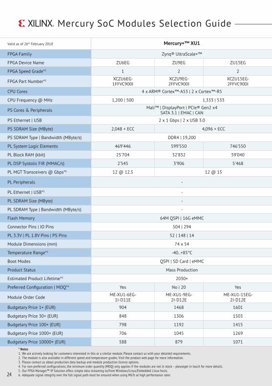
Mercury SoC Modules Selection Guide
24
* Notes1. We are actively looking for customers interested in this or a similar module. Please contact us with your detailed requirements.2. The module is also available in different speed and temperature grades. Visit the product web page for more information.3. Please contact us about production data backup and module production licence options.4. For non-preferred configurations, the minimum order quantity (MOQ) only applies if the modules are not in stock – pleaseget in touch for more details.5. Our FPGA Manager™ IP Solution offers simple data streaming to/from Windows/Linux/Embedded Linux hosts.6. Adequate signal integrity over the full signal path must be ensured when using MGTs at high performance rates
Valid as of 26th February 2018
FPGA Family
FPGA Device Name
FPGA Speed Grade*2
FPGA Part Number*2
CPU Cores
CPU Frequency @ MHz
PS Cores & Peripherals
PS Ethernet | USB
PS SDRAM Size (MByte)
PS SDRAM Type | Bandwidth (MByte/s)
PL System Logic Elements
PL Block RAM (kbit)
PL DSP Systolic FIR (MMAC/s)
PL MGT Transceivers @ Gbps*6
PL Peripherals
PL Ethernet | USB*5
PL SDRAM Size (MByte)
PL SDRAM Type | Bandwidth (MByte/s)
Flash Memory
Connector Pins | IO Pins
PL 3.3V | PL 1.8V Pins | PS Pins
Module Dimensions (mm)
Temperature Range*2
Boot Modes
Product Status
Estimated Product Lifetime*3
Preferred Configuration | MOQ*4
Module Order Code
Budgetary Price 1+ (EUR)
Budgetary Price 30+ (EUR)
Budgetary Price 100+ (EUR)
Budgetary Price 1000+ (EUR)
Budgetary Price 10000+ (EUR)
Mercury+™ XU1 Mercury+™ XU2
Zynq® UltraScale+™ Zynq® UltraScale+™
ZU6EG ZU9EG ZU15EG ZU4CG ZU5EV ZU7EV
1 2 2 1 1 2
XCZU6EG- 1FFVC900I
XCZU9EG- 2FFVC900I
XCZU15EG- 2FFVC900I
XCZU4CG-1FBVB900I
XCZU5EV-1FBVB900I
XCZU7EV-2FBVB900I
4 x ARM® Cortex™-A53 | 2 x Cortex™-R5 2 x A53 | 2 x R5 4 x ARM® Cortex™-A53 | 2 x Cortex™-R5
1,200 | 500 1,333 | 533 1,200 | 500 1,333 | 533
Mali™ | DisplayPort | PCIe® Gen2 x4 SATA 3.1 | EMAC | CAN
DP | PCIe® Gen2 x4SATA | EMAC | CAN
Mali™ | DisplayPort | PCIe® Gen2 x4SATA 3.1 | EMAC | CAN
2 x 1 Gbps | 2 x USB 3.0 2 x 1 Gbps | 2 x USB 3.0
2,048 + ECC 4,096 + ECC 2,048 + ECC 4,096 + ECC
DDR4 | 19,200 DDR4 | 19,200
469’446 599’550 746’550 192’150 256’200 504’000
25’704 32’832 59’040 18’432 23’616 38’880
2’545 3’906 5’468 939 1’362 2’678
12 @ 12.5 12 @ 15 12 @ 12.5 12 @ 15
- 2 x PCIe® Gen3 x8 H.265 Codec2 x PCIe® Gen3 x8
- -
- -
- -
64M QSPI | 16G eMMC 64M QSPI | 16G eMMC
504 | 294 504 | 294
52 | 148 | 14 52 | 148 | 14
74 x 54 74 x 54
-40..+85°C -40..+85°C
QSPI | SD Card | eMMC QSPI | SD Card | eMMC
Mass Production Advance*1
2030+ TBD
Yes No | 20 Yes TBD
ME-XU1-6EG- 1I-D11E
ME-XU1-9EG- 2I-D12E
ME-XU1-15EG- 2I-D12E
ME-XU2-4CG-1I-D11E
ME-XU2-5EV-1I-D12E
ME-XU2-7EV-2I-D12E
904 1468 1601 501 875 1184
848 1306 1503 470 821 1112
798 1192 1415 441 772 1046
706 1045 1269 380 682 932
588 879 1071 321 569 783

Zynq UltraScale+ modules
25
General notes• Not all features are available simultaneously – please check the documentation for any applicable constraints.• All specifications and release dates are subject to change without notice. Please verify component specifications with vendor’s datasheets.• Enclustra maintains an errata and revision history document for each product. Please also check the errata of the FPGA device and other components.• All prices are non-binding estimates – please contact us for definitive pricing and lead-time information.• Pricing during sampling starts significantly higher and decreases with time. Budgetary pricing typically starts 12 months after production FPGAs are available.• All trademarks are the property of their respective owners. All prices do not include shipping, taxes and duties.
Mercury+™ XU1 Mercury+™ XU2
Zynq® UltraScale+™ Zynq® UltraScale+™
ZU6EG ZU9EG ZU15EG ZU4CG ZU5EV ZU7EV
1 2 2 1 1 2
XCZU6EG-1FFVC900I
XCZU9EG-2FFVC900I
XCZU15EG-2FFVC900I
XCZU4CG- 1FBVB900I
XCZU5EV- 1FBVB900I
XCZU7EV- 2FBVB900I
4 x ARM® Cortex™-A53 | 2 x Cortex™-R5 2 x A53 | 2 x R5 4 x ARM® Cortex™-A53 | 2 x Cortex™-R5
1,200 | 500 1,333 | 533 1,200 | 500 1,333 | 533
Mali™ | DisplayPort | PCIe® Gen2 x4SATA 3.1 | EMAC | CAN
DP | PCIe® Gen2 x4 SATA | EMAC | CAN
Mali™ | DisplayPort | PCIe® Gen2 x4 SATA 3.1 | EMAC | CAN
2 x 1 Gbps | 2 x USB 3.0 2 x 1 Gbps | 2 x USB 3.0
2,048 + ECC 4,096 + ECC 2,048 + ECC 4,096 + ECC
DDR4 | 19,200 DDR4 | 19,200
469’446 599’550 746’550 192’150 256’200 504’000
25’704 32’832 59’040 18’432 23’616 38’880
2’545 3’906 5’468 939 1’362 2’678
12 @ 12.5 12 @ 15 12 @ 12.5 12 @ 15
- 2 x PCIe® Gen3 x8 H.265 Codec 2 x PCIe® Gen3 x8
- -
- -
- -
64M QSPI | 16G eMMC 64M QSPI | 16G eMMC
504 | 294 504 | 294
52 | 148 | 14 52 | 148 | 14
74 x 54 74 x 54
-40..+85°C -40..+85°C
QSPI | SD Card | eMMC QSPI | SD Card | eMMC
Mass Production Advance*1
2030+ TBD
Yes No | 20 Yes TBD
ME-XU1-6EG-1I-D11E
ME-XU1-9EG-2I-D12E
ME-XU1-15EG-2I-D12E
ME-XU2-4CG- 1I-D11E
ME-XU2-5EV- 1I-D12E
ME-XU2-7EV- 2I-D12E
904 1468 1601 501 875 1184
848 1306 1503 470 821 1112
798 1192 1415 441 772 1046
706 1045 1269 380 682 932
588 879 1071 321 569 783

Mercury SoC Modules Selection Guide
26
* Notes1. We are actively looking for customers interested in this or a similar module. Please contact us with your detailed requirements.2. The module is also available in different speed and temperature grades. Visit the product web page for more information.3. Please contact us about production data backup and module production licence options.4. For non-preferred configurations, the minimum order quantity (MOQ) only applies if the modules are not in stock – pleaseget in touch for more details.5. Our FPGA Manager™ IP Solution offers simple data streaming to/from Windows/Linux/Embedded Linux hosts.6. Adequate signal integrity over the full signal path must be ensured when using MGTs at high performance rates
Mercury+™ XK1
Kintex® UltraScale+™
KU3P KU11P
1 2
XCKU3P- 1FBVD900E
XCKU11P- 2FFVD900I
-
-
-
-
-
-
356’000 653’000
25’920 43’560
1’765 4’538
16 @ 12.5 16 @ 15
PCIe® Gen3 x16 4 x PCIe® Gen3 x16 2 x 150G | 100G
1 Gbps | FTDI USB 2.0
2,048 4,096
DDR4 | 9,600 DDR4 | 19,200
64M QSPI
504 | 246 504 | 294
66 | 100 | - 66 | 148 | -
74 x 54
0..+85°C -40..+85°C
Slave Serial | QSPI | USB2
Advance*1
TBD
TBD
ME-XK1-3P- 1E-D11
ME-XK1-11P- 2I-D12
TBD TBD
TBD TBD
TBD TBD
TBD TBD
TBD TBD
Valid as of 26th February 2018
FPGA Family
FPGA Device Name
FPGA Speed Grade*2
FPGA Part Number*2
CPU Cores
CPU Frequency @ MHz
PS Cores & Peripherals
PS Ethernet | USB
PS SDRAM Size (MByte)
PS SDRAM Type | Bandwidth (MByte/s)
PL System Logic Elements
PL Block RAM (kbit)
PL DSP Systolic FIR (MMAC/s)
PL MGT Transceivers @ Gbps*6
PL Peripherals
PL Ethernet | USB*5
PL SDRAM Size (MByte)
PL SDRAM Type | Bandwidth (MByte/s)
Flash Memory
Connector Pins | IO Pins
PL 3.3V | PL 1.8V Pins | PS Pins
Module Dimensions (mm)
Temperature Range*2
Boot Modes
Product Status
Estimated Product Lifetime*3
Preferred Configuration | MOQ*4
Module Order Code
Budgetary Price 1+ (EUR)
Budgetary Price 30+ (EUR)
Budgetary Price 100+ (EUR)
Budgetary Price 1000+ (EUR)
Budgetary Price 10000+ (EUR)

Kintex UltraScale+ and Zynq UltraScale+ modules
27
General notes• Not all features are available simultaneously – please check the documentation for any applicable constraints.• All specifications and release dates are subject to change without notice. Please verify component specifications with vendor’s datasheets.• Enclustra maintains an errata and revision history document for each product. Please also check the errata of the FPGA device and other components.• All prices are non-binding estimates – please contact us for definitive pricing and lead-time information.• Pricing during sampling starts significantly higher and decreases with time. Budgetary pricing typically starts 12 months after production FPGAs are available.• All trademarks are the property of their respective owners. All prices do not include shipping, taxes and duties.
Mercury+™ XK1
Kintex® UltraScale+™
KU3P KU11P
1 2
XCKU3P-1FBVD900E
XCKU11P-2FFVD900I
-
-
-
-
-
-
356’000 653’000
25’920 43’560
1’765 4’538
16 @ 12.5 16 @ 15
PCIe® Gen3 x16 4 x PCIe® Gen3 x162 x 150G | 100G
1 Gbps | FTDI USB 2.0
2,048 4,096
DDR4 | 9,600 DDR4 | 19,200
64M QSPI
504 | 246 504 | 294
66 | 100 | - 66 | 148 | -
74 x 54
0..+85°C -40..+85°C
Slave Serial | QSPI | USB2
Advance*1
TBD
TBD
ME-XK1-3P-1E-D11
ME-XK1-11P-2I-D12
TBD TBD
TBD TBD
TBD TBD
TBD TBD
TBD TBD
Mercury™ XU5
Zynq® UltraScale+™
ZU2EG ZU3EG ZU4EV ZU5EV ZU5EV
1 2 1 2 3
XCZU2EG- 1SFVC784I
XCZU3EG- 2SFVC784I
XCZU4EV- 1SFVC784I
XCZU5EV- 2SFVC784I
XCZU5EV- 3SFVC784E
4 x ARM® Cortex™-A53 | 2 x Cortex™-R5
1,200 | 500 1,333 | 533 1,200 | 500 1,333 | 533 1,500 | 600
Mali™ | DisplayPort | PCIe® Gen2 x4 SATA 3.1 | EMAC | CAN
1 Gbps | 2 x USB 3.0
2,048 + ECC 4,096 + ECC 8,192 + ECC
DDR4 | 19,200
103’320 154’350 192’150 256’200
5’400 7’776 18’432 23’616
310 558 939 1’637 1’882
- 4 @ 12.5
- H.265 Codec PCIe® Gen3 x4
1 Gbps
512 1,024 2,048
DDR4 | 4,266 DDR4 | 4,800 DDR4 | 4,266 DDR4 | 4,800
64M QSPI | 16G eMMC
336 | 178
52 | 92 | 14 52 | 72 | 14
56 x 54
-40..+85°C 0..+85°C
QSPI | SD Card | eMMC
Sampling
2030+
Yes No | 40 No | 40 Yes No | 20
ME-XU5-2EG- 1I-D11E
ME-XU5-3EG- 2I-D11E
ME-XU5-4EV- 1I-D11E
ME-XU5-5EV- 2I-D12E
ME-XU5-5EV- 3E-D13E
319 613 541 784 1162
298 509 507 735 1025
279 444 476 691 931248 380 428 624 825201 300 360 511 708

Mercury SoC Modules Selection Guide
* Notes1. We are actively looking for customers interested in this or a similar module. Please contact us with your detailed requirements.2. The module is also available in different speed and temperature grades. Visit the product web page for more information.3. Please contact us about production data backup and module production licence options.4. For non-preferred configurations, the minimum order quantity (MOQ) only applies if the modules are not in stock – pleaseget in touch for more details.5. Our FPGA Manager™ IP Solution offers simple data streaming to/from Windows/Linux/Embedded Linux hosts.6. Adequate signal integrity over the full signal path must be ensured when using MGTs at high performance rates
Mercury™ XU7
Zynq® UltraScale+™
ZU6EG ZU9EG ZU15EG
1 2 2
XCZU6EG- 1FFVC900I
XCZU9EG- 2FFVC900I
XCZU15EG- 2FFVC900I
4 x ARM® Cortex™-A53 | 2 x Cortex™-R5
1,200 | 500 1,333 | 533
Mali™ | DisplayPort | PCIe® Gen2 x4 SATA 3.1 | EMAC | CAN
2 x 1 Gbps | USB 3.0
2,048 + ECC 4,096 + ECC
DDR4 | 19,200
469’446 599’550 746’550
25’704 32’832 59’040
2’545 3’906 5’468
12 @ 12.5 12 @ 15
-
-
2’048 4’096
DDR4 | 8,532 DDR4 | 9,600
64M QSPI | 16G eMMC
336 | 178
52 | 52 | 14
74 x 54
-40..+85°C
QSPI | SD Card | eMMC
Advance*1
2030+
TBD
ME-XU7-6EG- 1I-D11E
ME-XU7-9EG- 2I-D12E
ME-XU7-15EG- 2I-D12E
954 1502 1667
886 1337 1556
824 1221 1456
720 1071 1296
600 904 1096
28
Valid as of 26th February 2018
FPGA Family
FPGA Device Name
FPGA Speed Grade*2
FPGA Part Number*2
CPU Cores
CPU Frequency @ MHz
PS Cores & Peripherals
PS Ethernet | USB
PS SDRAM Size (MByte)
PS SDRAM Type | Bandwidth (MByte/s)
PL System Logic Elements
PL Block RAM (kbit)
PL DSP Systolic FIR (MMAC/s)
PL MGT Transceivers @ Gbps*6
PL Peripherals
PL Ethernet | USB*5
PL SDRAM Size (MByte)
PL SDRAM Type | Bandwidth (MByte/s)
Flash Memory
Connector Pins | IO Pins
PL 3.3V | PL 1.8V Pins | PS Pins
Module Dimensions (mm)
Temperature Range*2
Boot Modes
Product Status
Estimated Product Lifetime*3
Preferred Configuration | MOQ*4
Module Order Code
Budgetary Price 1+ (EUR)
Budgetary Price 30+ (EUR)
Budgetary Price 100+ (EUR)
Budgetary Price 1000+ (EUR)
Budgetary Price 10000+ (EUR)

Zynq UltraScale+ modules
General notes• Not all features are available simultaneously – please check the documentation for any applicable constraints.• All specifications and release dates are subject to change without notice. Please verify component specifications with vendor’s datasheets.• Enclustra maintains an errata and revision history document for each product. Please also check the errata of the FPGA device and other components.• All prices are non-binding estimates – please contact us for definitive pricing and lead-time information.• Pricing during sampling starts significantly higher and decreases with time. Budgetary pricing typically starts 12 months after production FPGAs are available.• All trademarks are the property of their respective owners. All prices do not include shipping, taxes and duties.
Mercury™ XU7
Zynq® UltraScale+™
ZU6EG ZU9EG ZU15EG
1 2 2
XCZU6EG- 1FFVC900I
XCZU9EG- 2FFVC900I
XCZU15EG- 2FFVC900I
4 x ARM® Cortex™-A53 | 2 x Cortex™-R5
1,200 | 500 1,333 | 533
Mali™ | DisplayPort | PCIe® Gen2 x4 SATA 3.1 | EMAC | CAN
2 x 1 Gbps | USB 3.0
2,048 + ECC 4,096 + ECC
DDR4 | 19,200
469’446 599’550 746’550
25’704 32’832 59’040
2’545 3’906 5’468
12 @ 12.5 12 @ 15
-
-
2’048 4’096
DDR4 | 8,532 DDR4 | 9,600
64M QSPI | 16G eMMC
336 | 178
52 | 52 | 14
74 x 54
-40..+85°C
QSPI | SD Card | eMMC
Advance*1
2030+
TBD
ME-XU7-6EG- 1I-D11E
ME-XU7-9EG- 2I-D12E
ME-XU7-15EG- 2I-D12E
954 1502 1667
886 1337 1556
824 1221 1456
720 1071 1296
600 904 1096
Mercury+™ XU6
Zynq® UltraScale+™
ZU2EG ZU3EG ZU4EV ZU5EV ZU5EV
1 2 1 2 3
XCZU2EG- 1SFVC784I
XCZU3EG- 2SFVC784I
XCZU4EV- 1SFVC784I
XCZU5EV- 2SFVC784I
XCZU5EV- 3SFVC784E
4 x ARM® Cortex™-A53 | 2 x Cortex™-R5
1,200 | 500 1,333 | 533 1,200 | 500 1,333 | 533 1,500 | 600
Mali™ | DisplayPort | PCIe® Gen2 x4 SATA 3.1 | EMAC | CAN
2 x 1 Gbps | USB 3.0
2,048 + ECC 4,096 + ECC 8,192 + ECC
DDR4 | 19,200
103’320 154’350 192’150 256’200
5’400 7’776 18’432 23’616
310 558 939 1’637 1’882
- 4 @ 12.5
- PCIe® Gen3 x4 | H.265 Codec
2 x 1 Gbps | Cypress FX3™ USB 3.0
-
-
64M QSPI | 16G eMMC
504 | 270
96 | 120 | 14
74 x 54
-40..+85°C 0..+85°C
QSPI | SD Card | eMMC
Advance*1
2030+
TBD
ME-XU6-2EG- 1I-D11E
ME-XU6-3EG- 2I-D11E
ME-XU6-4EV- 1I-D12E
ME-XU6-5EV- 2I-D12E
ME-XU6-5EV- 3E-D13E
391 699 787 853 1295
366 583 665 800 1143
343 510 588 753 1038
291 423 494 664 905
228 328 408 537 771
29

Mercury SoC Modules Selection Guide
* Notes1. We are actively looking for customers interested in this or a similar module. Please contact us with your detailed requirements.2. The module is also available in different speed and temperature grades. Visit the product web page for more information.3. Please contact us about production data backup and module production licence options.4. For non-preferred configurations, the minimum order quantity (MOQ) only applies if the modules are not in stock – pleaseget in touch for more details.5. Our FPGA Manager™ IP Solution offers simple data streaming to/from Windows/Linux/Embedded Linux hosts.6. Adequate signal integrity over the full signal path must be ensured when using MGTs at high performance rates
Mercury™ ZX1 Mercury™ ZX5
Zynq®-7000 Zynq®-7000
Z-7030 Z-7035 Z-7045 Z-7015 Z-7030
2 1 2 2 1 3
XC7Z030- 2FBG676I
XC7Z035- 1FBG676I
XC7Z045- 2FFG676I
XC7Z015- 2CLG485I
XC7Z030- 1SBG485I
XC7Z030- 3SBG485E
2 x ARM® Cortex™-A9 2 x ARM® Cortex™-A9
800 667 800 766 667 1’000
2 x CAN 2 x CAN
1 Gbps | USB 2.0 OTG 1 Gbps | USB 2.0 OTG
1,024 1,024
DDR3L | 4,264 DDR3L | 4,264 DDR3L | 5,333
125’000 275’000 350’000 73’920 125’000
9’540 18’000 19’620 3’420 9’540
520 981 1’170 176 438 593
4 @ 6.6 8 @ 6.6 8 @ 10.3125 4 @ 6.25 4 @ 6.6
PCIe® Gen2 x4 PCIe® Gen2 x8 PCIe® Gen2 x4
2 x 100 Mbps -
256 -
DDR3L | 2,133 DDR3L | 1,600 DDR3L | 3,200 -
64M QSPI | 512M NAND 64M QSPI | 512M NAND
334 | 170 334 | 178 334 | 178
66 | 84 | 12 66 | 72 | 12 146 | - | 12 54 | 92 | 12
64 x 54 56 x 54
-40..+85°C -40..+85°C 0..+70°C
QSPI | SD Card | NAND QSPI | SD Card | NAND
Mass Production Mass Production
2030+ 2030+
Yes Yes Yes Yes Yes No | 40
ME-ZX1-30- 2I-D10
ME-ZX1-35- 1I-D10
ME-ZX1-45- 2I-D10-P
ME-ZX5-15- 2I-D10
ME-ZX5-30- 1I-D10
ME-ZX5-30- 3C-D10
429 752 995 275 323 483
393 697 926 265 306 441
359 602 819 256 290 404
297 483 647 204 246 288
226 347 496 157 184 201
30
Valid as of 26th February 2018
FPGA Family
FPGA Device Name
FPGA Speed Grade*2
FPGA Part Number*2
CPU Cores
CPU Frequency @ MHz
PS Cores & Peripherals
PS Ethernet | USB
PS SDRAM Size (MByte)
PS SDRAM Type | Bandwidth (MByte/s)
PL System Logic Elements
PL Block RAM (kbit)
PL DSP Systolic FIR (MMAC/s)
PL MGT Transceivers @ Gbps*6
PL Peripherals
PL Ethernet | USB*5
PL SDRAM Size (MByte)
PL SDRAM Type | Bandwidth (MByte/s)
Flash Memory
Connector Pins | IO Pins
PL 3.3V | PL 1.8V Pins | PS Pins
Module Dimensions (mm)
Temperature Range*2
Boot Modes
Product Status
Estimated Product Lifetime*3
Preferred Configuration | MOQ*4
Module Order Code
Budgetary Price 1+ (EUR)
Budgetary Price 30+ (EUR)
Budgetary Price 100+ (EUR)
Budgetary Price 1000+ (EUR)
Budgetary Price 10000+ (EUR)

Zynq-7000 modules
General notes• Not all features are available simultaneously – please check the documentation for any applicable constraints.• All specifications and release dates are subject to change without notice. Please verify component specifications with vendor’s datasheets.• Enclustra maintains an errata and revision history document for each product. Please also check the errata of the FPGA device and other components.• All prices are non-binding estimates – please contact us for definitive pricing and lead-time information.• Pricing during sampling starts significantly higher and decreases with time. Budgetary pricing typically starts 12 months after production FPGAs are available.• All trademarks are the property of their respective owners. All prices do not include shipping, taxes and duties.
Mercury™ ZX1 Mercury™ ZX5
Zynq®-7000 Zynq®-7000
Z-7030 Z-7035 Z-7045 Z-7015 Z-7030
2 1 2 2 1 3
XC7Z030- 2FBG676I
XC7Z035- 1FBG676I
XC7Z045- 2FFG676I
XC7Z015- 2CLG485I
XC7Z030- 1SBG485I
XC7Z030- 3SBG485E
2 x ARM® Cortex™-A9 2 x ARM® Cortex™-A9
800 667 800 766 667 1’000
2 x CAN 2 x CAN
1 Gbps | USB 2.0 OTG 1 Gbps | USB 2.0 OTG
1,024 1,024
DDR3L | 4,264 DDR3L | 4,264 DDR3L | 5,333
125’000 275’000 350’000 73’920 125’000
9’540 18’000 19’620 3’420 9’540
520 981 1’170 176 438 593
4 @ 6.6 8 @ 6.6 8 @ 10.3125 4 @ 6.25 4 @ 6.6
PCIe® Gen2 x4 PCIe® Gen2 x8 PCIe® Gen2 x4
2 x 100 Mbps -
256 -
DDR3L | 2,133 DDR3L | 1,600 DDR3L | 3,200 -
64M QSPI | 512M NAND 64M QSPI | 512M NAND
334 | 170 334 | 178 334 | 178
66 | 84 | 12 66 | 72 | 12 146 | - | 12 54 | 92 | 12
64 x 54 56 x 54
-40..+85°C -40..+85°C 0..+70°C
QSPI | SD Card | NAND QSPI | SD Card | NAND
Mass Production Mass Production
2030+ 2030+
Yes Yes Yes Yes Yes No | 40
ME-ZX1-30- 2I-D10
ME-ZX1-35- 1I-D10
ME-ZX1-45- 2I-D10-P
ME-ZX5-15- 2I-D10
ME-ZX5-30- 1I-D10
ME-ZX5-30- 3C-D10
429 752 995 275 323 483
393 697 926 265 306 441
359 602 819 256 290 404
297 483 647 204 246 288
226 347 496 157 184 201
31

MERCURY+ PE1PCIe® Base Board
� Mercury module connectors � Low-jitter clock generator � PCIe ×4 interface � USB 3.0 device � Up to 4 × USB 2.0 � FTDI USB 2.0 High-speed device controller � 2 × Gigabit Ethernet � Up to 2 FMC LPC/HPC connectors � mPCIe/mSATA card holder � microSD card holder � 12 V single supply � 160 × 111.2 mm (PCB only) � Standalone or PCIe operation � Available in three configurations (PE1-200/300/400)
ME-PE1-200-C
1+ €269
100+ €248
1000+ €218
10000+ €193
Mercury+ PE1
microSD Card Holder
SMA MGT + Clocks
mSATA/ mPCIe
Card Holder
SIM Card Holder
USB 3.0 Device
eMMC Flash JTAG Connector
System Controller
Clock Generator
USB Hub
Pin HeaderPin Header Micro USB Power Control
System Monitor
Battery Holder
FMC LPC Connector
FMC HPC Connector
Pin Headers
DC Input Connector
Current Sense
Buttons & LEDs
Mod
ule
Conn
ecto
r A
Module Connector C
Mod
ule
Conn
ecto
r B
Gigabit Ethernet
(x2)
USB 2.0 Host (x2)
32

MERCURY+ PE3PCIe® Base Board
� Mercury module connectors � PCIe Gen3 ×8 interface � QSFP+ slot, optional 4 × SFP+ slots � Low-jitter clock generator � USB-C interface � 3 × USB 2.0 host � 3 × Gigabit Ethernet � Up to 2 FMC HPC connectors � microSD card holder � System controller with USB JTAG/UART � Standalone or PCIe operation � 12V single supply or USB-C powered � Preliminary product information – please contact us for availability.
Preliminary product information – please contact us for availability.
Mercury+ PE3
96 I/Os
72 I/Os
8 MGTs
8 MGTs
76I/Os
4 MGTs
4 MGTs
PCIe Gen2 ×8
4 MGTs8 MGTs
26 I/Os
PL
PL
PL
PL
PL
PL
HA/HB
LA
LA
DP DP
Key Variant-dependent I/O options Optional features
Note that this diagram shows a reduced feature set.
Gigabit Ethernet
(x2)
MGT Multiplexers
Power Control
SFP+ Slots (x4)
FMC HPC Connectors
Top Bottom
QSFP+ Slot
microSD Holder
Gigabit Ethernet
USB C
USB AUSB Mux & Hub
Gigabit PHY
FMC HPC Connectors (x2)
Top Bottom
System MonitorMicro USB DC Input
Connector
Mod
ule
Conn
ecto
r B
Module Connector C
Mod
ule
Conn
ecto
r A
System Controller
Clock Generator
CIk/Trig I/O
Pin Header
Battery Holder
JTAG Connector
33

Mars EB1
HDMI Connector
DC Input Connectors
Power Control
Buttons & LEDs
System Monitor
Mini Camera Link Connector
Mini Camera Link Connector
Gigabit Ethernet Connector
System Controller
200-pin Mars Module SO-DIMM Connector
USB 2.0 A Connector (Host) Micro USB
Micro USB
microSD Card Holder
JTAG Connector
Pmod™ I/O Pin Headers
Anios™ I/O Pin Header
34
MARS EB1Mars Base Board
� Mars module connector � FTDI USB 2.0 High-Speed device � 2 × Mini Camera Link � HDMI 1.3 connector � Micro USB 2.0 device � microSD card slot � 42 user I/O pins � 40-pin Anios headers � 2 user buttons, 1 user LED � 12 V single supply � 120 × 80 mm
MA-EB1-C
1+ €214
100+ €190
1000+ €160
10000+ €136

MARS PM3Mars Base Board
� Mars module connector� FMC LPC connector� Mini HDMI connector� Cypress FX3 USB 3.0 device controllerw� USB 2.0 UART� Gigabit Ethernet� microSD card slot� 12 V single supply� p-ITX format (100 × 72 mm)
MA-PM3-C
1+ €210
100+ €185
1000+ €136
10000+ €116
JTAG | GPIO
USB 3.0
16/32-bit
USB 2.0
UART MDI 4 +1 pairsUSB
JTAG
24 I/Os
36 pairs
Mars PM3
USB 3.0 B Connector (Device)
Cypress FX3 USB 3.0 Device Controller
System Monitor
User EEPROM
Power Supply
Fan Connector
Power Connectors
200-pin Mars Module SO-DIMM Connector
Bottons & LEDs
HDMI Connector
(LVDS/PCIe)
USB 2.0 A Connector (Host)
RJ45 GigE Connector
USB 2.0 Micro-B Connector (Device)
USB 2.0 UART Controller
FX3 ConnectorFPGA JTAG Connector
160-pin FMC LPC Connector
Extension Connector
35

� FMC LPC connector � 6 MOSFET half-bridges � 42 V 18 A power capability � CAN � 30 V sensor input and actor outputs � An ideal platform to evaluate the Enclustra Universal Drive Controller IP Core
SPI
PWM
I2C
LVCMOS
LVCMOS
LVCMOS
30V
Enc/Hall
CAN
30 V I/O Connectors
Motor Connectors 1-3
Supply Connector
Encoder Connector 1-3
CAN ConnectorCAN Transceiver
A/D Converters
MOSFET Drivers
Temperature Sensors
Encoder | Hall Sensor Signal Conditioning
30 V I/O Signal Conditioning
Current Sense Amplifiers
Brake Chopper
FMC LPC Connector
Half Bridges 1- 6
36
FMC DR2Drive Control Card
FMC-DR2
1+ €682
100+ €520
1000+ €197
10000+ €154

OS support:
� Xilinx® Zynq®-7030/7035/7045 SoC FPGA � PCIe or standalone operation � 1 GB DDR3L SDRAM (PS) � 256 MB DDR3L SDRAM (PL) � 16 GB eMMC flash � 64 MB QSPI flash � 8 × 6.6/10.3125 Gbps MGT � PCIe Gen2 ×8 interface � QSFP+ slot, optional 4 × SFP+ slots � Up to 2 × FMC HPC connectors, 168 User I/Os � 4 × USB 2.0 host, USB-C interface � Gigabit Ethernet, 2 × Fast Ethernet � System controller with USB JTAG/UART � Low-jitter clock generator � 12V single supply or USB-C powered � 166.4 × 111.2 mm CO-XZQ10-740-I
1+ €1343
100+ €1118
1000+ €851
10000+ €679
COSMOS XZQ10PCIe® System Board
37
PS
PS
96 I/Os
72 I/Os
4-8 MGTs4 MGTs
4 MGTs
PCIe Gen2 ×8
4 MGTs8 MGTs
16-bit
24 I/Os
PL
PS
PLPLPS
PL
PL
HA/HB
LA
LA
DP DP
Key Variant-dependent I/O options Optional features
Note that this diagram shows a reduced feature set.
Fast Ethernet
(x2)
System Controller
eMMC Flash
Clock Generator
Pin Header
USB Pin Header
MGT Multiplexers
Power Control
FMC HPC Connectors
Top Bottom
System Monitor
Battery Holder
CIk/Trig I/O
JTAG Connector
QSFP+ Slot
Micro USB DC Input Connector
microSD HolderQSPI Flash
Gigabit Ethernet
32-bitPS | PL
DDR3 SDRAM
USB C
DDR3 SDRAM
USB AUSB Hub
USB Mux
FMC HPC Connectors (x2)
Top Bottom
SFP+ Slots (x4)

A huge logo, for a tool that saves a huge amount of time.
Our Linux Build Environment is a free tool which users can use to build their own Linux for Enclustra modules – at the push of a button.
Select a target module and base board, let the tool do its thing, and all required binaries, such as the FPGA bitstream and boot loader, will be
downloaded. It also downloads and compiles software such as U-Boot, Linux, and the BusyBox based root file system. Find out more
via our website.
38
L inux Build Environment
FPGA DESIGN Center

An applicationThe Module Configuration Tool (MCT) is a free application which allows the user to configure our modules and base boards via USB, without additional hardware. No break-out boxes, no funky connectors – all you need is a USB cable.
A libraryThe library used by the MCT, MctLib, is also available free of charge in binary form; it allows users to integrate module enumeration, FPGA and SPI flash configuration, and I2C communication functionality in their own applications.
MctLib is available for both Windows and Linux, and consists of a flexible library with a C-style interface, allowing use of the library from almost any programming language. For C++ applications, a C++ wrapper is also provided for ease of use.
A flexible codebaseIf you’d like to integrate or customize the Module Configuration Tool to your needs, we also offer a source code license for both the GUI and the MctLib library. Contact us for more information.
» Module Configuration Toolkit
39FPGA DESIGN Center
In order to make integrating our products to customer designs as easy as possible, we provide a number of design support files to make
the process as pain-free as possible.
» Design Suppor t
3D ModelsFor all of our modules and base boards, 3D models are available to aid in the design of compatible custom hardware and enclosures.
User SchematicsHow the components on our hardware talk to each other.
Master PinoutsCheck the pinout of a module or base board, and compare it with other pin-compatible modules, even future modules that haven’t been released yet.
User ManualsEverything you always wanted to know about a module, but were afraid to ask: an A-Z of a module’s hardware, features, and configuration options.
Reference designsOur reference designs are lovingly created to get your design off the ground as quickly, in both HDL and software.
Net Length TablesHigh-speed design is tricky; net length tables give you exactly what you need to best plan for signal routing and integrity.
Online SupportFor anything that isn’t covered in the information above, our support staff are always on hand to help, even before purchase.
FPGA DESIGN Center40

We offer a range of flexible IP solutions, covering a range of applications areas; here are a couple
of things worth knowing:
They’re royalty freeAfter you purchase an IP licence, that’s it; no recurring fees, no royalties, nada. The IP can be used perpetually, according to the licence terms.
We offer different licence modelsThe licence itself can also be tailored to your requirements. We offer project and site-based licences.
Evaluation is also freeYou can evaluate our IP solutions, with full functionality, before committing to buy. Just drop us a mail.
» Our IP Solutions
41

High-performance FPGA/SoC motion control – without writing a line of VHDL. A highly optimized IP solution, featuring implementations of commonly-used motor control algorithms for position, velocity and current control, as well as all required interfaces to the power electronics. A simple and portable C programming API allows easy access to all features from software.
Features and benefits � Control up to 8 motors simultaneously
� Control loop update rates of up to 200kHz
� Fully autonomous event handling
� Supports BLDC, DC and stepper motors
� Features field-oriented control for BLDC motors
Flexibility is key � Full support for custom circuits for current,
position and velocity measurement
� Specify which controls loops are autonomous
and which are implemented in software
UNIVERSAL DRIVE CONTROLLERIP Solution
Integration and ease of use � C programming API to access all features
� Full integration with Xilinx® tools
� Reference designs available for all motor types
Evaluation � A free IP evaluation licence including reference
design and example application is available
� Start with a spinning motor using a quick-start
kit including an SoC module, base board, power
electronics and motor. For more information
see next page.
42
IP Core
Starting from €3000
Controller Core
Encorder | Resolver Interface
Encorder | Resolver Interface
Encorder | Resolver Interface
Drive Hardware
Error Handler
Avalon/AXI Interface
Galvanic Isolation (optional)
Encorder | Resolver Interface
Encorder | Resolver Interface
ENC
RES
DC
BLDC
Stepper
DA
Universal Drive Controller IP Core

Get started with the Universal Drive Controller, right out of the box. The Universal Drive Controller Evaluation Kit provides an out-of-the box hardware platform with reference design to both speed your development time and enhance your productivity.
The kit contains: � Universal Drive Controller Evaluation Licence,
with support for up to 2 DC, BLDC or stepper motors
� Mars ZX3 SoC module
� Mars PM3 base board
UNIVERSAL DRIVE CONTROLLEREvaluation Kit
� FMC-DR2 drive control card
� BLDC (Maxon), DC or stepper motor
� Reference design
� 2 hours of support
43
Evaluation Kit
€1490

One tool for all FPGA communications. Transparently stream up to 16 data streams from FPGA to host, and vice versa, without needing to know the underlying protocols. PCIe® (Gen1-3, ×1-×8), USB 2.0, USB 3.0, and 10/100/1000 Mbps Ethernet links – all with one single API. Also supported are FPGA-in-the-loop applications, and memory-mapped access.
Software library � Simple API with intuitive read/write functions
� Supports C | C++, C# | .NET and MATLAB
� Supports Windows and Linux
FPGA IP core � Supports standard bus interfaces
� Integrates into FPGA vendor tools for simple drag
and drop instantiation
� Also available as a software implementation
for PCs (FPGA modelling) or SoC FPGAs
(co-processing)
FPGA MANAGERIP Solution
44
IP Solution
Starting from €6750
Matlab®
Base licence � PCIe, USB 3.0, USB 2.0 or Gigabit Ethernet
� 2 streams
� C | C++ and C# | .NET
� Windows or Linux
Evaluation � Quick Start Kits, including support,
are available
FPGA Manager™
FPGAHost/Embedded PC
PCIe
Ethernet
USB 2.0 / 3.0
–or–
–or–FPGA
Manager Library
(DLL/SO)
FPGA Manager IP Core
User Application
C | C++, C# | .NET and
MATLAB®
User Logic

Get started with the FPGA Manager, right out of the box. The FPGA Manager™ Evaluation Kit provides a full featured design platform to build communication centric applications for PCIe®, Ethernet and USB 3.0. The kit provides an out- of-the box hardware platform with reference design to both speed your development time and enhance your productivity. It contains following components.
The kit contains: � FPGA Manager IP Solution, Evaluation License
� Reference design
� Mercury KX1 FPGA module
FPGA MANAGEREvaluation Kit
� Mercury+ PE1-200 base board
� Power supply
� 2 hours support included
45
Evaluation Kit
€990

Large, multi-stream FIFO handling. A versatile IP core that implements a stream to memory mapped DMA bridge with up to 16 independent streams. The IP core allows data buffering in an external memory device to provide virtual FIFO capability, with up to 4 GB of memory. A simple C programming API is provided, as is the option to easily integrate with FPGA Manager™.
Features and benefits � Standalone solution A CPU can be easily replaced
by a stream configuration controller that is
provided in VHDL
� Flexible data width conversion Conversion
to/from any byte-multiple width for the write and
read data streams
� Highly configurable Operation mode, buffer
size and buffer address can be set independently
for each stream
� Vendor independent The core is optimized for
use in current Xilinx® FPGA architectures. Xilinx
Vivado IPI components are also provided.
STREAM BUFFER CONTROLLERIP Core
Evaluation � FIFO mode Writes and reads are done over the
AXI4-Stream interfaces
�Write mode Writes are done over the AXI4-Stream,
reads are done by a CPU
� Read mode Writes are done by a CPU, reads are
done over the AXI4-Stream interface
� ROM mode Reads are done over the AXI4-Stream
interface (the memory must be initially written
by a CPU)
46
IP Core
Starting from €3750
Stream Buffer Controller IP Core
Host/Embedded PC
Status | IRQ
Data
Config
External Memory
CPU
Memory Controller
Stream Buffer Controller
IP Core
Data Sources
Data Sinks
AXI |
Ava
lon
Inte
rconn
ect

Low-resource display control, with support for different display interfaces. The Display Controller IP Core enables the easy addition of a display to existing or future FPGA designs, allowing the system designer to focus on the main application instead of dealing with display control issues. In addition, there is no need for an external display controller device that would consume precious PCB space and unnecessarily extend the project’s BOM. With its modular design and strong scalability, the Display Controller IP Core perfectly fits the system requirements without wasting any FPGA resources. These unique features will also simplify the reuse of the Display Controller IP Core in future projects. Selecting our Display Controller IP Core for the display control needs of present or future projects will significantly reduce time to market as well as the overall system cost.
Features and benefits � Support for parallel, LVDS and HDMI/DVI displays without
external display controller device
� Support for unlimited video pages
� Built-in PWM generator for display brightness control
� Optional 2D accelerator unit (draw/copy rectangles, supports transparent color)
� AXI bus interface for both register bank and frame buffer memory access
DISPLAY CONTROLLERIP Core
47
IP Core
Starting from €2250
Display Controller IP Core
FPGA/SoC Device
2D DataLVDS | HDMI |
Parallel
Touch
Video Data
External Memory
Display Hardware
CPU
Memory Controller Stream
Controller IP Core
I2C Controller
AXI |
Ava
lon
Bus
Config

Simple Ethernet communication, without a CPU. A highly configurable IP core, optmised for use in current Xilinx® FPGA architectures. It provides a simple to use interface to the user logic, and supports the common media independent interfaces MII, RMII, GMII and RGMII. With its 8-bit wide transmit and receive interfaces running at 125 MHz, the IP core is able to operate at full 1 Gbit/sec wire speed. 100 Mbit/sec and 10 Mbit/sec operation is also supported.
Features and benefits � Operates at full 1 GBit/sec wire speed
� Complete UDP, IPv4 and Ethernet layer processing
� Automatic ARP reply generation
� Header pass-through mode
� 1 Gbit/sec, 100 Mbit/sec and 10 Mbit/sec
operation
� MII, RMII, GMII, RGMII and SGMII media indepen-
dent interfaces (full-duplex only)
UDP/IP ETHERNETIP Core
� Destination UDP port, destination IP address
and destination MAC address filtering
� UDP checksum calculation and check
� Ethernet frame check
� Multiple UDP ports with dedicated receive
and transmit interfaces for each port
� Optional receive data buffers
� Raw Ethernet port for non-UDP communication
48
IP Core
Starting from €3600
Key User clock domain Ethernet PHY clock domain
Dual Fast Ethernet
Dual Fast Ethernet
Quad SFP+ Slots
(optional)
Quad SFP+ Slots
(optional)
Quad SFP+ Slots
(optional)
Quad SFP+ Slots
(optional)
DC Input Connector
ARP Protocol Engine
microSD Holder
Gigabit Ethernet
Dual USB ARGMII
GMII
RMII
Mii
User Transmit Header
Interface
User Transmit Data Interface
User Receive Data Interface
User Configuration Interface
UDP/IP Ethernet IP Core

PricingPricing is shown for specific module variants and quantities – for a complete list of module variants, and volume pricing for quantities of 1+, 30+, 100+, 300+, 1000+, 3000+ and 10000+, visit www.enclustra.com
Custom configurations All hardware products can be tailored to specific applications in custom configurations (different FPGA part numbers, different memory sizes, etc.).
Custom hardware design We often work together with customers to develop a brand new, application-specific hardware product. This can be a module, base board, or entire system; development costs and production rights are shared, leaving both parties to benefit.
FAQ More information and frequently asked questions can be found at www.enclustra.com/faq
Disclaimer All prices are non-binding estimates – please contact us for definitive pricing and lead-time information. Information contained in this flyer is correct as of 26th February 2018, but is subject to change without notice. Trademarks used are property of their respective owners.
» Fur ther Information
49

Catalogue Spring 2018
Development and design services
FPGA DESIGN Center

2
About Enclustra
We currently have 33 people in our team, of 10 different nationalities, and we’re growing.
The company was founded in 2004 by Martin Heimlicher, with the aim of providing comprehensive FPGA solutions, from design through to production.
Our headquarters are located in the thriving Binz quarter in Zürich, Switzerland – an ideal location in one of the world’s leading cities for technology and innovation.
In addition to our main office, we have sales and support offices in Germany, the USA and China.
Demand for our design services, FPGA modules and base boards is growing – our current customer base stands at over 1000 customers in over 50 countries, and continues to expand.
2

CERTIFIED MEMBER — BASE
We’re vendor-independent, and we’re design service partners of Xilinx® – this close communication allows us to be forward-looking in our design process, and remain on
the cutting edge of the most advanced FPGA technology.
3
Everything from the drawing board.
FPGA Design Center
Our design center offers design and support in all areas of FPGA-based system development, in a wide number of applications.
High-speed hardware, HDL firmware, embedded software, real-time operating systems – our expertise covers every stage of the design process, from specification up to industrialization and manufacturing.
Everything off the shelf.
FPGA Solution Center
We develop and sell our own FPGA and system-on-chip modules, based on Xilinx® devices, for our customers to integrate into their own systems.
19 different modules, in 3 different families, compatible with 3 different base boards – the diversity of our products allows the customer to select exactly the features and they need, down to a fine grain.
W
W
O
H
E
F
A
F
T
E R

4
» Our Core Competencies
FPGA Hardware Development
• Multi-layer PCB design• Multi-gigabit serial links• High-speed data converters• RF front ends
Digital Signal Processing
• Bit-true MATLAB®/Simulink® to VHDL conversion• Resource-optimized implementation• Software defined radio (channel filtering, sample rate
conversion, modulation/demodulation, etc.)
Software Development
• Embedded software for SoC and soft core processors• Real-time control loops• Linux BSPs and device drivers• Host computer software as user interface to FPGA-based systems
FPGA HDL Development
• Systems at the technical limits (complexity, bandwidth, processing power, latency)
• Integration of microcontrollers and peripherals• Thorough verification and continuous integration• HLS or HDL design entry
FPGA DESIGN Center

We carry out customer projects in a wide array of application fields – below are some of the areas we’re particularly
experienced in.
Wired Networks and Switching (Ethernet)
Industrial Communication (CAN)
Wireless Communication (Software Defined Radio)
Embedded Interfaces (PCIE, USB, AXI, etc.)
Drive and Motion Control
Computer Vision and Smart Cameras
Test and Measurement / Data Acquisition
Waveform Synthesis
FPGA DESIGN Center
» Main Applicat ion Areas
5

» Digital Signal Processing
Manual, bit-true HDL implementation.
Do you have a MATLAB® implementation of a signal processing algorithm and need a best performance, lowest resource usage and lowest power FPGA implementation? Our engineering team has successfully completed a significant number of such projects with the help of our fixed-point arithmetics library.
Our cl_fix library implements basic to medium-complexity fixed-point arithmetic functions in MATLAB and VHDL. The implementations of the same function in MATLAB and VHDL show exactly the same, bit-accurate behavior. The functions operate on the native data types of the individual languages; i.e. double for MATLAB and std_logic_vector for VHDL, and are thus easy to use. The bit-true behavior is enabled by associating a fixed-point format to every operand and result.
We take care of the algorithm’s FPGA-optimization, and work with you to ensure that the FPGA-optimized MATLAB algorithm still meets your requirements. After that, it’s a straightforward path to a bit-true FPGA implementation, without any lengthy and costly iterations back through the algorithm design and optimization phases.
Model-based design and automated HDL code generation.
If traceability or time to market is the main concern for the FPGA implementation of your MATLAB/Simulink® signal processing algorithm, model-based design and automated HDL code generation might also be a useful option.
We’re a member of MathWorks’ partner program, and our engineering team has the relevant expertise to efficiently employ automated code generation tools like MathWorks® HDL Coder™, Xilinx® System Generator (Simulink) and alike.
As an additional benefit, your application specialists – who not necessarily are FPGA experts – are able to develop your FPGA’s signal processing units in their known environment and programming language, while we take care of the communication infrastructure and interfaces.
FPGA DESIGN Center6

» Perspective through stereo
What was once only possible in crime series is now a reality (get your CSI
Miami one-liners at the ready): 3D scans of forensic evidence found at
crime scenes, recording minute details to be later analyzed from all angles.
One of the main elements of the system is an Enclustra-developed
platform which enables the projection of interference patterns and
simultaneous recording of stereo video: a compact, cost-effective Mars
AX3 module captures the images via two cameras connected to the new
Mars EB1 base board via Camera Link. The FPGA firmware running on
the Mars AX3 then streams the data to a host PC via Enclustra’s FPGA
Manager Ethernet IP solution.
The development took place as part of the 3D-Forensics project funded
by the EU’s Seventh Framework Programme for Research (FP7).
Xilinx® Artix™-7 | DDR3 SDRAM | Camera Link | Gigabit Ethernet |
Xilinx MicroBlaze™ | VHDL | C | C#
FPGA System Design | FPGA Hardware | FPGA HDL | Embedded Software |
Host Computer Software
Mars AX3 | Mars EB1 | FPGA Manager™ Ethernet
Abstract
Employed Technologies
Involved Enclustra Services
Involved Enclustra Products
FPGA DESIGN Center
Example project #1
7

Example project #2
» FPGA to Satell i te: Please Respond
A reliable data connection between satellite and ground station is
essential to the success of any satellite mission – to this end, we recently
implemented a system for a customer based on our Mercury KX1
module and using FPGA Manager™ PCI Express.
The Mercury KX1, mounted on custom PCIe®-capable base board we also
developed for the application, acts as the main communication
controller for a test system that is used to verify the communication
between individual satellite components as well as the communication
between the satellite and the ground station.
The host computer software, providing a GUI for setting up, running
and analyzing communication tests, was also developed by our engineering
team.
Xilinx® Kintex®-7 | WizardLink | VHDL | C# | C++
FPGA System Design | FPGA Hardware | FPGA HDL | Host Computer
Software
Mercury KX1 | FPGA Manager PCIe
Abstract
Employed Technologies
Involved Enclustra Services
Involved Enclustra Products
FPGA DESIGN Center8
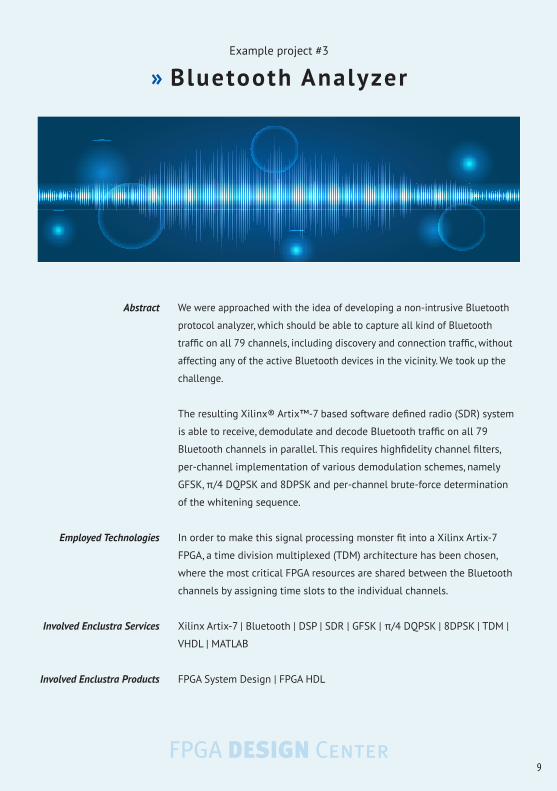
Example project #3
» Bluetooth Analyzer
We were approached with the idea of developing a non-intrusive Bluetooth
protocol analyzer, which should be able to capture all kind of Bluetooth
traffic on all 79 channels, including discovery and connection traffic, without
affecting any of the active Bluetooth devices in the vicinity. We took up the
challenge.
The resulting Xilinx® Artix™-7 based software defined radio (SDR) system
is able to receive, demodulate and decode Bluetooth traffic on all 79
Bluetooth channels in parallel. This requires highfidelity channel filters,
per-channel implementation of various demodulation schemes, namely
GFSK, π/4 DQPSK and 8DPSK and per-channel brute-force determination
of the whitening sequence.
In order to make this signal processing monster fit into a Xilinx Artix-7
FPGA, a time division multiplexed (TDM) architecture has been chosen,
where the most critical FPGA resources are shared between the Bluetooth
channels by assigning time slots to the individual channels.
Xilinx Artix-7 | Bluetooth | DSP | SDR | GFSK | π/4 DQPSK | 8DPSK | TDM |
VHDL | MATLAB
FPGA System Design | FPGA HDL
Abstract
Employed Technologies
Involved Enclustra Services
Involved Enclustra Products
FPGA DESIGN Center9

Requirements definition | Use cases
Customer Enquiry
Free Commercial Offer Creation
Hardware Production HDL Implementation System Software Implementation
System Deployment
Concept Engineering
Detailed Hardware Design Detailed HDL Design Detailed Software Design
System Integration & Test
Requirements Engineering
Project Preparation
System Maintenance
Hardware Bringup & Test HDL Integration & Test Software Integration & Test
» Our Development Process
FPGA DESIGN Center
Project team setup | Project management setup | Kick-off
Purchase Order
Maintenance | Support | Follow-up projects
Customer Acceptance
Integration of building blocks | Top-level tests and simulation Design documentation update | Peer reviews
Rough concept | Feasibility evaluation | Risk analysis Rough effort/cost estimation
Detailed design of building blocks | Design documentation Peer reviews
System integration (HW, HDL and SW) | System-level tests Design documentation update
Project scope | Project schedule | Binding effort/cost estimation
Implementation of building blocks | Block-level tests and simulation | Design documentation update | Peer reviews
Release creation and delivery | Customer training Customer acceptance tests
10

» Contact
USAKevin McCluskeyUSA Representative+1 978 835 3941
Asia聂崇岭 | Chongling Nie 中国区代表 | China Representative+86 138 1116 3451
GermanyKlaus Schwan Sales Representative Germany+49 (0) 8095 870977
Germany/FranceGuy EschemannSales and Engineering Representative Germany+49 (0) 7851 6366305
Enclustra GmbHRäffelstrasse 28
8045 ZürichSwitzerland
+41 43 343 39 43 [email protected]
11Copyright © 2018 Enclustra GmbH. All rights reserved.