carbon material growth, characterization, and device
TRANSCRIPT

Carbon Material Growth, Characterization, and
Device Fabrication
by
Solomon Mikael
A dissertation submitted in partial fulfillment
of the requirement for the degree of
Doctor of Philosophy
(Electrical Engineering)
at the
University of Wisconsin Madison
2015
Date of final oral examination: 12/14/2015
The dissertation is approved by the following members of the Final Oral Committee:
Zhenqiang “Jack” Ma (Advisor), Professor, Electrical Engineering
Shaoqin “Sarah” Gong, Professor, Biomedical Engineering
Michael Corradini, Professor, Engineering Physics
Mikhail Kats, Professor, Electrical Engineering
Zongfu Yu, Professor, Electrical Engineering

© Copyright by Solomon Mikael 2015
All Rights Reserved

i
To Anyone Taking The Less Traveled Path

ii
Acknowledgements
I would never have been able to finish this dissertation without the guidance of my
committee, professors, and help from my colleagues and friends.
I would like to express my sincere gratitude to my advisor Professor Zhenqiang (Jack)
Ma for offering me a position in his group at the University of Wisconsin Madison. His constant
support and input helped guide many of the projects I worked on through my Ph.D. study. I
would also like to thank Professor Shaoqin (Sarah) Gong, Professor Douglass Henderson,
Professor Michael Corradini, Professor Mikhail Kats, and Professor Zongfu Yu, for their
insightful comments and valuable suggestions on the research I worked on.
I would also like to thank Mr. Winslow Sargent for his generous support during my Ph.D
studies and The Graduate Engineering Research Students program (GERS) at the University of
Wisconsin Madison. Both of these programs provided support and encouragement throughout
my Ph.D studies. Both helped me reach goals I could have not reached on my own. Thank you.
I am thankful for the opportunity to work in Prof Ma’s research group and participate in
many research topics. I had the chance to meet many intelligent and thoughtful people during my
stay and wish them the best of luck in their lives and careers. Last but not least I’d like to thank
my family for their support over the years. Thank you.

iii
Abstract
The research of using different carbon allotropes has steadily developed over the years.
One of the allotropes of interest is graphene because of its unique optical and electronic
properties. Bilayer graphene unlike monolayer graphene has the potential to have the bandgap
modified. To date the largest bandgap opening for bilayer graphene is 250meV, but was done
locally (~10um) with very large bias voltages. A critical step to see materials like bilayer
graphene leave the lab is introducing wafer scale methods for electronic band modification. This
work will present the use of straining films to apply wafer scale stress to sheets of bilayer
graphene to modify the electrical properties of bilayer graphene. Using FTIR and raman
spectroscopy a bandgap of ~40meV was observed in large areas (~100umx100um).
The use of transparent neural electrode arrays with ultra-flexibility and biocompatibility
would provide an optimal platform for various applications, including optogenetics and neural
imaging. Neural electrode arrays with broad-wavelength transparency from the ultraviolet (UV)
to infrared (IR) spectrums are especially desirable, and provide unique opportunities to advance
these techniques that would otherwise be impossible with conventional opaque metal electrodes.
Also, the transparent neural electrode allows for simultaneous observation of tissue response
during optical or electrical stimulation. Graphene, a novel two dimensional carbon-based
material, is one of the most promising candidates because the material has a UV to IR
transparency of over 90 % in addition to its high electrical and thermal conductivity, flexibility,
and biocompatibility. Here we present a protocol for the fabrication of the transparent graphene

iv
neural electrode array and its operation for electrophysiology, fluorescent microscopy, optical
coherence tomography (OCT), and optogenetics
Finding appropriate measurement techniques in high temperature high radiation
environments present several challenges. This work will also introduce the development of a
temperature sensor for high radiation environments. Currently the most sensitive high
temperature thermocouples have sensitivities in the uV/C range. Next generation nuclear reactors
will have temperature ramps and power densities that will exceed the capabilities of current
thermocouples. I propose using single crystal boron doped diamond diode as a replacement for
next generation reactor temperature sensing. Due to its large bangap the sensitivity of the device
can be as high as mV/C allowing for detailed recording of quick temperature changes. In
addition to the high sensitivity the carbon in diamond and boron are two materials that are highly
radiation resistant allowing reliable operation over large fluxes and durations. I will show the
current progress on this project and the future plans for in-pile testing.
Replicating the human eye using conventional semiconductor materials and devices has
been a goal of photodetector arrays for many years. Artificial Eyes using silicon nanomembranes
on flexible polyimide substrates have been demonstrated. The device in conjuncture with the
collection setup and software allow for many of the unique capabilities of the human eye to be
realized in a process that is compatible with current semiconductor tools and methods.

v
TABLE OF CONTENTS
Acknowledgements……………….…………………….…………………………………….ii
Abstract………………………………………...………………………………………………iii
List of Figures…………………………………………………………………………….…viii
List of Tables……………………………………………………………………………..…xxii
List of Equations…………………………………………………………………….…….xxiii
CHAPTER 1 Introduction………………………………………………………………………1
1.1 Introduction and Motivation…………………………………………………….….…………1
1.2 Graphene’s Properties…………………………………………………………………………2
1.2.1 Graphene lattice and Band Structure……………………………...………………...2
1.2.2 Electronic Properties…………………………………………………………...……5
1.2.3 Optical Properties……………………………………………………………………9
1.3 Motivation and Objectives……………………………………………………...……………14
1.4 Synthesis of Monolayer and Bilayer Graphene………………………………………...……15
1.5 Dissertation Outline……………………………………………………………….…………22
Chapter 2 Bandgap Modification of AB Stacked Bilayer Graphene……………………..…23
2.1 Introduction and Motivation…………………………………………………………………24

vi
2.2 Strain Engineering of Graphene………………………………………………...……………26
2.3 Experimental Techniques & Results…………………………………………………………32
2.4 Discussion & Future Work………………………………………………………..…………68
2.5 Summary………………………………………………………………………………..……70
Chapter 3 Transparent Electrodes for Brain Implants………………………………………71
3.1 Introduction and Motivation…………………………………………………………………71
3.2 Current Methods for Brain Signal Recording…………………………………..……………72
3.3 Carbon Layered Electrode Array (CLEAR) Brain Electrode……………………..…………73
3.4 Future Work & Summary……………………………………………………………………82
Chapter 4 High Sensitivity Diamond Temperature Sensor………………….………………83
4.1 Introduction and Motivation…………………………………………………………………83
4.2 Diamond Properties………………………………………………………………….………84
4.3 Growth of Single Crystal Diamond………………………………………….………………92
4.4 Fabrication of PI Diodes for high sensitivity Temperature Sensors……………………..…111
4.5 Future Work & Summary……………………………………………………………..……118
Chapter 5 Electrical Artificial Human Eye Photo-detector Array……………...…………119
5.1 Introduction…………………………………………………………………………………119

vii
5.2 Background of Artificial Human Eye………………………………………………………120
5.3 Electrical Characterization and Image Acquisition…………………………………...……122
5.4 Summary……………………………………………………………………………………123
Chapter 6 Conclusion and Future Work……………………………………….……………125
6.1 Conclusions…………………………………………………………………………………125
6.2 Future Work……………………………………………………………………...…………125
6.3 References…………………………………………………………………………..………126

viii
List of Figures
Figure 1.1 Graphene in 0 dimensions (buckyball), 1 dimension (carbon nanotube), 2 dimensions
(graphene), and 3 dimension (graphite)…………………………………………………………...3
Figure 1.2 Graphene’s structure [1] and unit cell for both mono layer and bilayer graphene. The
unit cell for monolayer graphene has 2 atoms in it while bilayer unit cell has 4 atoms. The
rhombus is the conventional unit cell, The γ terms represent the energy of the bonding between
the respective atoms in graphene………………………………………………………………….4
Figure 1.3 Reciprocal lattice of monolayer and bilayer graphene with lattice points shown as
black dots, b1 and b2 are primitive reciprocal lattice vectors. The shaded hexagon is the first
Brillouin zone with Γ indicating the centre, and K + and K − showing two non-equivalent
corners……………………………………………………………………………………………..6
Figure 1.4 H = transfer integral matrix = describes the hopping of the π electrons between the
different carbon atoms, S = overlap integral matrix = gives us the strength of the overlap of the π
orbital's on different atoms, f (k) describes nearest-neighbor hopping. The respective gamma (γ)
terms describe interatomic hopping parameter between different combinations of atoms in the
unit cell………………………………………………………………………………………….…7
Figure 1.5 The energy dispersion for bilayer and monolayer graphene. The expression for the
energy is calculated by solving the determinate mentioned earlier in Equation 1.3. (a) shows the
monolayer dispersion where E(k) = ± kvF and for (b) bilayer graphene *2
22
m
kE
.(Michael S.
Fuhrer, University of Maryland) = planks constant, Fv = Fermi velocity, m* = effective mass
of electron in bilayer graphene…………………………………………………………………....8

ix
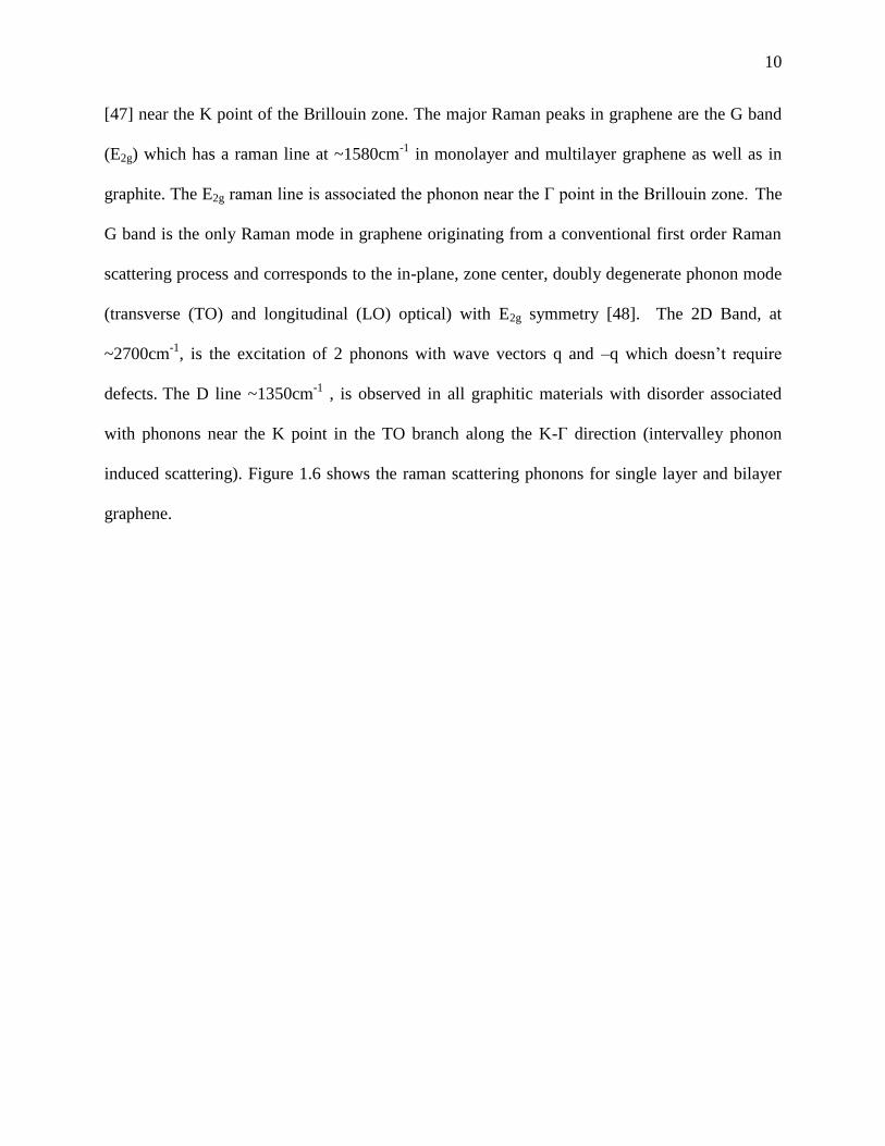
Figure 1.6 The types of raman bands in monolayer and bilayer graphene can be divided into (i)
defect inducted modes where the additional momentum to get total momentum transfer is almost
equal to zero is provided by elastic scattering from defects (ii) excitation of tow phonons with
wave vectors q and -q which doesn’t require any defect induced scattering for wave vector
compensation.[2]………………………………………………………………………………..11
Figure 1.7 The γ coupling terms have been observed in the Slonczewski-Weiss-McClure (SWM)
Tight binding model and been experimentally observed using Raman, FTIR, and photoemission.
For bulk bilayer graphene γ0=2.9eV, γ1=0.3eV, γ3=0.1eV, and γ4=0.12eV [3]…………..……13
Figure 1.8 The low pressure chemical deposition (LPCVD) growth system. Major components
include the furnace, label 1, flow meters, label 2, pressure sensors, label 3, and mechanical
pump, label 4. (b) The computer controls using for the LPCVD system, consisting of the
computer control system, label 5, flow controllers, label 6, and power supplies, label 7……….17
Figure 1.9 Show the growth recipies with both temperature and pressure plotted on the y-axis (a)
shows the entire growth process from start to fininsh (b) is a magnified version of the process
distinguishing the different steps in the growth process, anneal, monolayer growth, and bilayer
growth…………………………………………………………………………………………....20
Figure 2.1 (a) Top and bottom gated structure with exfoliated bilayer graphene [4] (b) Using
uniaxial strain the sample substrate is stretched while one of the layers is pinned down [5] (c)
Theoretical paper proposing using strain in bilayer graphene to open the bandgap and the
calculated change in the E(k) of the sample [6]…………………………………………...……25

x
Figure 2.2 Shows the process for growing the sample and the wet chemistry needed to get the
final graphene sample on a silicon substrate for further device processing…………………..…28
Figure 2.3 The graphene sample in different stages of processing (a) right after removal from the
LPCVD system (b) optical image of graphene on the copper foil (c) the graphene sample on Si
SiO2 (300nm) substrate (d) optical image of monolayer graphene on Si SiO2 (300nm) substrate
(e) optical image of bilayer graphene on Si SiO2 (300nm) substrate (f) scanning electron
microscope (SEM) of bilayer region on the monolayer graphene……………………………….29
Figure 2.4 The raman data for three types of graphene that are present in the LPCVD grown
material. The purple raman signal is for monolayer graphene. The green raman signal is for
bilayer graphene, and the red raman signal is for trilayer graphene…………………………..…30
Figure 2.5 The figure shows an atomic force microscopy (AFM) scan one of the bilayer regions.
The step between the stacked layers is visible in the AFM. The 0.5nm step between the layers is
close to the monolayer graphene thickness. Below a profile of the scan over the center of the
stack is shown………………………………………………………………………………...….31
Figure 2.6 (a) Schematic illustration of the layered structure of strained bilayer graphene with a
Si3N4 stressor layer. (b) Measured tensile (top)/compressive (bottom) stress values from the
layered structure which is described in Figure 1(a) with respect to the Si3N4 layer with various
thicknesses. Blue and red plots denote the stress value of a Si3N4 layer generated using a high
and medium stress Si3N4 recipe. (c) and (d) Microscopic images of the bilayer graphene layer
transferred on 4” SiO2/Si substrate before deposition of Si3N4 stressor layers. (e) Illustrations
showing the formation of wrinkles by tensile or compressive Si3N4 stressor layers (f) A

xi
microscopic image of the bilayer graphene layer after deposition of the tensile Si3N4 stressor
layer. (g) A microscopic image of the bilayer graphene layer after deposition of the compressive
Si3N4 stressor layer. The insets in Figure 1 (f) and (g) are the angled SEM images of the strained
bilayer graphene. Scale ………………………………………………..33
Figure 2.7 Microscopic images taken from (a) low compressively stressed and (b) highly
compressively stressed graphene. The images show different dimensions of wrinkles formed by a
low and high compressive Si3N4 stressor layer, respectively. The sample with a low compressive
Si3N4 stressor layer shows an average width of 2.96 μm, while the sample with a highly
compressive Si3N4 stressor layer shows an average width of 4.43 μm. Overall the wrinkles
formed by a high stressor layer have wider wrinkles. However, it is also noted that wrinkles
mostly formed around the bilayer graphene regions as indicated by white arrows……………...38
Figure 2.8 (a) A schematic cross section of the layered structure of the samples with different
degree of strains (Green: Low stress, Red: Medium stress, Blue: High stress). “Layer 1” and
“Layer 2” indicate the bottom and top graphene layer, respectively. (b) Raman shifts of the G
band (left) and 2D band (right) induced by the Si3N4 tensile stressor layer taken on the wrinkles
graphene region. (c) Raman shifts of the G band (left) and 2D band (right) induced by the Si3N4
tensile stressor layer taken on the bilayer graphene regions. (d) Raman shifts of the G band (left)
and 2D band (right) shifts induced by the Si3N4 compressive stressor layer taken on the wrinkles
graphene region. (e) Raman shifts of the G band (left) and 2D band (right) induced by the Si3N4
compressive stressor layer taken on the bilayer graphene regions……………………………....39

xii
Figure 2.9 (a) Illustration of the structures of the samples (left) without and (right) with the
Si3N4 stressor layer. Raman spectra compare the (b) G peak and (c) 2D peak without and with
the low stress Si3N4 layer. This shows that a low tensile stress (~15 MPa) does not change the G
peak position notably and only caused a minor blue-shift in the 2D peak position……………..41
Figure 2.10 (a) The measured sheet resistance under three different conditions, i.e. a bilayer
graphene (1) without any Si3N4 layer on top, (2) with a low stress Si3N4 layer, and (3) with a
highly compressive stress Si3N4 layer. (b) Microscopic images of the device used to measure the
sheet resistance. It should be noted that the result did not show any noticeable graphene sheet
resistances for case (1) and (2), whereas case (3) showed 70 % lower sheet resistance. It is
believed that the low sheet resistance is mostly caused by the high Si3N4 stressor layer, since the
effect by the deposition of Si3N4 layer or unwanted doping from the SiO2/Si substrate can be
ruled out. The average sheet resistance values for each case are 41 Ω, 48.6 Ω, and 27.3 Ω with
…………………………………..43
Figure 2.11 (a) A microscopic image of the wrinkles graphene. The arrows indicate the
measured spots and the colors of the arrows match each plot in Figure 2.11(b)-(c). (b) Raman
shifts of the G band and (c) 2D band measured by line scanning from the red region (body of the
wrinkle) to blue region (tail of the wrinkle), showing G band was spitted into two peaks (G+ and
G-) at the tail of the wrinkle. (d) A microscopic image of the wrinkles graphene indicating two
different spots with different degrees of compressive strains. The white arrows indicate the
bilayer graphene regions. (e) Raman shifts of the G band and (f) 2D band of the wrinkles

xiii
graphene taken at spot "a" and spot "b" shown in Figure 3(d). Red plots indicate the Raman
spectra taken from the “Low stress” Si3N4 layer as a reference…………………………………46
Figure 2.12 (a) Raman mapping of the highly compressive strained bilayer graphene (scan area:
100 μm2). Light blue and yellow indicate G band red-shifting. Yellow also indicates G band
splitting. Yellow indicates the location of G band splitting. (b) The overlay image of Raman
mapping and the microscopic image of the locations of splitting can be seen nearly all over the
sample……………………………………………………………………………………………48
Figure 2.13 The FTIR spectra and microscopic images of the strained bilayer graphene with a
red-arrow showing the line scanning direction. (a) high and (b) medium tensile stressed bilayer
graphene samples, respectively, (c) high and (d) medium compressive stressed bilayer graphene
samples, respectively. The band transitions that gave rise to the absorption spectra are shown for
the bilayer graphene (e) with Eg = 0 and (f) with Eg ≠ 0………………………………………...51
Figure 2.14 FTIR spectra taken over graphene with a low stress Si3N4 layer. For this particular
scan, the majority of the signal came from the Si/SiO2 substrate in the 1000 cm-1
to 200 cm-1
region. This shows that the Fabry Perot effect is difficult to completely remove from the
collected sample. The characteristic absorption peaks in the higher wavenumber values were not
observed. The absorption of single and bilayer graphene was very low resulting in the gold
standard distorting the final collected absorption………………………………………………..53
Figure 2.15 The FTIR spectra((a) and (c) and the respective Tauc’s method calculation of the
interband transitions((b) and (d) for the tensilely and compressively stressed measurements.(a)
and(b)for the high compressive-stressed sample,(c) and(d) for the high tensile-stressed sample.55

xiv
Figure 2.17 FTIR spectra of two monolayer samples stacked ontop of one another. The two
monolayers of graphene are placed one ontop of the other and a stressor layer of Si3N4 is applied
to the stack. The absorption spectrum shows minimal absorption (<1%) in the area relevant to
bilayer graphene……………………………………………………………………………….…57
Figure 2.18 Graphical illustration of the method of creating multiaxial strain by patterning
various number of spokes to generate (a) biaxial strain, (b) triaxial strain, (c) quadriaxial strain
and (d) quadriaxial axial strain, respectively, as examples……………………………………....59
Figure 2.19 Schematic illustrations and images of the fabrication process for creating triaxial
tensile strain in bilayer graphene. (i) Preparation of the CVD grown bilayer graphene. (ii) A
hexagonal shape patterning on a bilayer grpahene. (iii) Deposition of Cr claps to fix the patterned
graphene layer. (iv) Deposition of Si3N4 stressor layer on entire surface to apply a strain. (b) An
illustration to show the mechanism of the formation of tristar shape wrinkle. (c)-(e) Microscopic
images, corresponding to step (ii) – (iv). (f)-(g) Microscopic images after the deposition of low
and high Si3N4 stressor layers. Wrinkles are formed clearly. (h) A tilted SEM image taken at the
tristar shaped wrinkle…………………………………………………………………………….60
Figure 2.20 A measurement of the dimension of tristar wrinkle (Left) by SEM image and (Right)
calculation of its’ height……………………………………………………………………….....63
Figure 2.21 Raman shifts of the G band (a) and 2D band (b) on the tristar shape wrinkled
graphene induced by the Si3N4 tensile stressor with different degree of strains (Red: un-strained,
Green: low strained, Blue: high strained)………………………………………………………..65

xv
Figure 2.22 Raman shifts of the G band (a) and 2D band (b) on the tristar shape wrinkled
graphene induced by the Si3N4 tensile stressor with different degree of strains (Red: un-strained,
Green: low strained, Blue: high strained)………………………………………………………..66
Figure 2.23 (a) An AFM image to show the three dimensional surface profile of tristar shape
wrinkled bilayer graphene after the deposition of a Si3N4 tensile stressor layer. Inset show the top
view of the scanned region. (b) Simulated triaxial tensile strained graphene with high tensile
stressed Si3N4 layers by COMSOL Multiphysics………………………………………………..67
Figure 2.24 (A) shows a schematic of a bilayer RF graphene transistors without a straining gate
dielectric. (B) an optical image of the structure (C & D) Scanning electron microscope (SEM)
images of the bilayer RF transistor. The gate length of the transistor is 140 nm and source-to-
drain gap is 500 nm. The total gate width of two fingers is 12 μm……………………………...69
Figure 3.1 CLEAR device. a. Basic fabrication process: i. Metal patterning of traces and
connection pads on Parylene C/silicon wafer. The silicon wafer is the handling substrate. ii.
Transfer and stack four mono layers of graphene sequentially. iii. Graphene patterning to form
electrode sites. iv. Second Parylene C deposition and patterning to form device outline. v.
Removal of device from silicon wafer. b. Diagram of CLEAR device construction showing the
layered structures. c. Demonstration of CLEAR device flexibility. The device is wrapped around
of glass bar with a radius of 2.9 mm. d. Rat-sized CLEAR device: outlined by white dashed line.
e. Close-up of rat-sized device showing transparent graphene electrode sites and traces on a
Parylene C substrate. This side touches brain surface. Scale bar represents 500 µm. f. Mouse-
sized CLEAR device with ZIF PCB connector……………………………………………….…73

xvi
Figure 3.2 (a) shows the reduction of the sheet resistance as the number of layer stacked is
increased (b) compares the percentage of transmitted light since the laser light is 472nm it’s
critical that the transparent electrode has high transmission in that region of the spectrum (c)
compares the sheet resistance vs the transmission of a variety of metals and transparent
electrodes CLEAR aka graphene device is shown as a start and is comparable to many of the
materials but with much higher transmission capabilities……………………………………….76
Figure 3.3 In vivo recorded signal characterizations. a. Average longitudinal 1 kHz impedance
values for CLEAR and platinum micro-ECoG devices implanted in the same animal………….78
Figure 3.4 Optogenetic experiment (a) Schematic drawing of opto-experiment setup showing the
graphene/CLEAR device implanted on the cerebral cortex of a mouse with the light being
delivered by an optical fiber to stimulate the neural cells (b) Image of blue laser light stimulation
being delivered through the CLEAR/graphene device implanted on the cortex of a Thy1::ChR2
mouse. c. Optical evoked potentials recorded by the CLEAR device. d. Post-mortem control
data, with light impingent on electrode site 11, as is apparent by the stimulus artifact visible in
the signal for that channel. X-scale bars represent 50 ms, y-scale bars represent 100 µV……....79
Figure 3.5 In vivo imaging experiment. a. Bright-field image of CLEAR device implanted on the
cerebral cortex of a mouse beneath a cranial window. b. Fluorescence image of same device
shown in a. Mouse was given an intravenous injection of FITC-Dextran to fluorescently label the
vasculature. c. and d. Higher magnification bright-field and fluorescence images of same device
shown in a and b, respectively e. and f. Bright-field and fluorescence images of standard rat-

xvii
sized micro-ECoG array with platinum electrode sites, respectively. Scale bars in a-d represent
250 µm, while scale bars in e and f represent 750 µm…………………………………………..81
Figure 4.1 A comparison of the properties of Type IIa diamond and silicon………………...…84
Figure 4.2 Diamond unit cell with the cubic lattice structure, the lattice dimensions is about 0.36
nm and the interatomic distances are about 0.154 nm [7]………………………………….…85
Figure 4.3 The classification of different types of diamond, the different impurity levels, colors,
etc……………………………………………………………………………………………...…87
Figure 4.4 Band structure of diamond as calculated from the linear muffin tin orbital (LMTO)
method in the local-density approximation.[8]…………………………………………….….88
Figure 4.5 Comparison of diamond bandgap and dopant locations to other popular
semiconductor like Silicon, Germanium, and Gallium Nitride and the locations of the Fermi
levels for P type and N type doped materials. The bottom left plot [9] shows the resistivity and
type of conduction versus the concentration of boron acceptors at room temperature. The bottom
left image shows the conductivity in p-type diamond as a function of energy levels of boron
acceptors and temperature [10]………………………………………………………………....91
Figure 4.6 The compiled phase diagram for carbon [11]. There are two regions of interest CVD
and HPHT these two methods have allowed the creation of synthetic diamond at a much faster
rate that can be naturally mined………………………………………………………………….93
Figure 4.7 Rayleigh–Bénard convection occurs in a plane horizontal layer of fluid heated from
below, in which the fluid develops a regular pattern of convection cells known as Bénard cells.94

xviii
Figure 4.8 (a) shows the gas temperature T in Kelvin for a comparable PECVD reactor. (b)
shows the hydrogen atomic mole fraction as a percentage for substrate holder with a diameter of
9mm and power density ~120Wcm-3
(c) shows the C2 and (d) the CH3 mole fraction expressed as
a percentage [12]…………………………………………………………………………….….95
Figure 4.9 A simplified version of the Bachmann triangle showing the diamond growth region in
addition to regions where no growth and non-diamond growth occurs………………………….97
Figure 4.10 Illustration of the SiNM preparation and diffusion process for diffusion doping of
single crystal <100> Ib diamond. i. Heavy boron implantation on an SOI wafer and thermal
annealing to realize heavily doped top Si on SOI. ii. Heavily boron doped top Si layer released as
SiNM by selective etching of SiO2 . iii. Top Si picked up by an elastomeric stamp. iv. SiNM
transferred to a diamond plate. v. Bond forming between SiNM and diamond and thermal
diffusion with RTA. vi. SiNM removed by potassium hydroxide (KOH) etching………………98
Figure 4.11 Raman spectroscopy of three types of diamond, Green plot is natural Ib diamond,
Blue plot is synthetic high pressure high temperature (HPHT) diamond, and the red is synthetic
PECVD diamond. The blue dots are carbon while the white dots are hydrogen. If there is C-H
streaching the optical phonons will show up at ~3300cm-1
while if it’s only C-C stretching there
will be a strong peak at 1330cm-1
and another peak at 1550cm-1
……………………………..…99
Figure 4.12 Comparison of three types of synthetic diamond. The first left image is synthetic
PECVD diamond, the middle left is synthetic PECVD diamond with nitrogen incorporation, the
middle right is boron doped PECVD grown on a synthetic PECVD substrate, and the right image
is a heavily boron doped synthetic diamond sample……………………………………..…….101

xix
Figure 4.13 SIMS profile for boron for (a) PECVD grown samples (b) and diffusion doped
sample (c)shows the profile for additional materials that get incorporated into the film during
growth which include Si , N , O, and H………………………………………………………...103
Figure 4.14 Shows the effect on the XPS data as a reulst of the high conductively layer and a
fabricated device using the HCL as a diode at room temperature (green), 100oC (blue), and
200oC (red)………………………………………………………………………………...……104
Figure 4.15 Optical profilometry of the diamond samples showing very smooth (100) surfaces
with roughness RMS values <5nm……………………………………………………….…….107
Figure 4.16 FTIR spectra of several diamond samples. This compares the natural diamond to the
synthetic diamond spectra. For the natural diamonds the one phonon absorption peak as well as
the two phonon absorption peak is present. For the synthetic diamonds only the two phonon
absorption peak is present……………………………………………………………………....109
Figure 4.17 Diffusion doped diamond diode with XPS data. Shows the the SiNM also diffuses
nitrogen and silicon in addition to the boron. Great deal of leakage current as a result of this. The
smaller peaks to the right ~105eV and ~160eV correspond to Si incorporation into the to layers
of the lattice from diffusion ~4% in the lattice. Also nitrogen is also incorporated at ~408eV..117
Figure 4.18 Boron has two naturally occurring and stable isotopes, 11
B (80.1%) and 10
B (19.9%)
- 10
B is used in boron neutron capture therapy. The carbon in diamond is nearly all 12
C

xx
Lithium has two stable isotopes, 6Li (7.59%) and
7Li (92.4%) – the nuclear cross section of
6Li
940 barns while 7Li is 45mbarns [ 1 barn = 10
-28 m
2 ] making
7Li less affected by neutron
irradiation [KSU (P. Ugorowski) ]……………………………………………………………...112
Figure 4.19 The samples were irradiated with an average fast flux of ~ 2.63E+12 [n/cm2
s] and a
flux greater than 2.9eV of ~ 6.511E+11[n/cm2
s] for 15 minutes. This time attempts to replicate
the conditions the samples will experience during real operation……………………………...113
Figure 4.20 The left shows the ideal diode equation after some algebra extracting the sensitivity
which has the materials band gap in the exponent. The right plot shows how diamonds band gap
changes over a wide temperature range (<1%) meaning the sensitivity will stay the same even as
the environment changes [13]…………………………………………………………………115
Figure 4.21 The structure of the PECVD grown diamond and the respective IV curve from the
devices. The IV shows little leakage current while having ideality factors close to one……....116
Figure 4.22 The proposed design for the capillary for insertion into the reactor. The diode will
be inside the capillary and placed next to the fuel and the two connectors will be treaded through
an insulating material……………………………………………………………………..…….117
Figure 5.1 (a) Microscope picture of the doped membrane with etching holes. Different colors
indicate two types of doping. Shapes of each photodiode are marked out. (b), Microscope picture
for the finished silicon photodiode. Two metal layers clearly form interdigitated connection...121

xxi
Figure 5.2 (a) shows the optical setup for image creation (b) shows the convave photo detector
array (c) and (d) show the collected image using Labview and Matlab to extract and process the
collected IV data from the pixels……………………………………………………………….123

xxii
List of Tables
Table 1. Si3N4 film PECVD parameters and the measured stress on the layered samples
consisting of 25 nm Si3N4/20 nm SiO2/100 nm SiO2/ Si substrate…………………………...….35

xxiii
List of Equations
Equation 1.1 The lattice unit vectors/primitive lattice vectors for graphene……………………..4
Equation 1.2 The primitive lattice vectors which are related to the primitive lattice vectors by:
a1∙b1=a2∙b2=2π and a1∙b2=a2∙b1=0……………………………………………………………….....5
Equation 1.3 Solving the determinate will allow for the calculation of the energy levels (Ej) in
monolayer and bilayer graphene………………………………………………………………..…7
Equation 1.4 Expression for the boundary layer as a function of position on the sample……...18
Equation 1.5 The expression for the diffusion flux rate as a function of position……………..18
Equation 2.1 Expression for calculating the amount of strain in the graphene films using the
Raman data……………………………………………………………………………………….34
Equation 2.2 Expression for calculating the amount of strain in the graphene films using the
Raman data………………………………………………………………………………….……42
Equation 2.3 Equation for Tauc’s method for calculating the bandgap of a material based on the
optical absorption………………………………………………………………………………...54
Equation 2.4 Expression for the calculation of the Gruneisen parameter…………………..…..64
Equation 4.1 Position of second atom in the primitive unit cell in diamond lattice…………….86
Equation 4.2 Position of second atom in the primitive unit cell in diamond lattice…………….86
Equation 4.3 The reciprocal lattice basis vectors where V is the volume of the unit cell where i,
k , j = 1,2,3………………………………………………………………………………….…86

xxiv
Equation 4.4. Expression for the energy of electrons in the valence band maximum…………..89
Equation 4.5 Expression for the energy of an electron in the conduction band minima………..89
Equation 4.6 Expressions for the concentration of holes and the intrinsic charge carrier…...…89
Equation 4.7 The concentration of holes in the valence band due to boron…………………….90

1
CHAPTER 1 Introduction
The exponential growth of Si-based CMOS technology is rapidly approaching an end as
scaling down beyond the 10 nm node reaches fundamental physical limits [14]. The aggressive
scaling of CMOS devices has induced many drawbacks which include a dramatic increase in
fabrication costs, short-channel effects, high-field effect, quantum effect, gate leakage, process
variation, and heat dissipation issues. In the near future the cost of scaling of Si-based CMOS
will outweigh the benefits. One of the most promising candidates is graphene, which has
attracted a great deal of attention for electronic devices ever since its discovery in 2004 [15]. Its
material properties, such as intrinsic carrier mobility, saturation velocity, thermal conductivity,
and current carrying capacity, are far superior to those of silicon; moreover, its atomically thin 2-
D structure is naturally compatible with standard CMOS-based technologies. However graphene
is a gapless semimetal which is a large obstacle to overcome to be the next successor to silicon.
Thus, opening and tuning the band gap is the critical key for wider adoption of graphene for
electronic applications.
I will also introduce the development of a temperature sensor for high radiation
environments. Currently the most sensitive high temperature thermocouples have sensitivities in
the uV/C range. Next generation nuclear reactors will have temperature ramps and power
densities that will exceed the capabilities of current thermocouples. I propose using single crystal
boron doped diamond diode as a replacement for next generation reactor temperature sensing.
Due to its large bangap the sensitivity of the device can be as high as mV/C allowing for detailed
recording of quick temperature changes. In addition to the high sensitivity diamond and boron
are two materials that are highly radiation resistant allowing reliable operation over large fluxes

2
and durations. I will show the current progress on this project and the future plans for in-pile
testing.
In this dissertation the research work will focus on the growth, characterization and
straining of bilayer graphene. It will also include the growth, characterization and development
of a radiation hard temperature sensor. The thesis is organized as follows. Chapter 1 reviews the
electronic properties of graphene and reviews how others have modified the energy band
structure. Chapter 2 Will discuss the straining technique developed. Chapter 3 will look at
another application for graphene as a replacement for transparent electrodes for use in reading
brain signals in vivo. Chapter 4 will discuss the growth of single crystal diamond and the
development of the diamond diode. Chapter 5 will describe the artificial eye photo detector and
the image processing used to collect the data
1.2 Graphene’s Properties
1.2.1 Graphene lattice and Band Structure
Graphene has attracted a great deal of attention because of many unique optical and electrical
properties it has. Graphene has attracted widespread attention because of its superior properties
and enormous potential for various applications [16]. Graphene is the basis of all graphitic forms.
Graphene can be wrapped up into 0D buckyball, rolled into 1D nanotube, and stacked into 3D
graphite as shown in Figure 1.1 [17].

3
Figure 1.1 Graphene in 0 dimensions (buckyball), 1 dimension (carbon nanotube), 2
dimensions (graphene), and 3 dimension (graphite).
Monolayer graphene is a single atomic layer of sp2 bonded carbon atoms. The carbon atoms are
organized in a two dimensional hexagonal lattice structure as shown in Figure 1.2. The unit cell
of graphene has two carbon atoms with interatomic spacing of 0.1421nm [18]. The lattice unit
vectors are expressed as:

4
2
3,
2
3
2
3,
2
3
2
1
aa
aa
Equation 1.1 The lattice unit vectors/primitive
lattice vectors for graphene.
(a)
(b)
Figure 1.2 Graphene’s structure [1] and unit cell for both mono layer and bilayer graphene. The
unit cell for monolayer graphene has 2 atoms in it while bilayer unit cell has 4 atoms. The
rhombus is the conventional unit cell, The γ terms represent the energy of the bonding between
the respective atoms in graphene.
The sp2 hybridization between the s and both px and py orbital’s forms the covalent C-C bonds
between the carbon atoms. This bond is called the σ bond and forms the honeycomb lattice
structure in graphene material. The sp2 hybrids have three electrons for σ bonding. One electron
remains in a π-orbital which is known as pz. This pz orbital forms the valence π and conduction
band π* as a result of the hybridization. Bilayer graphene is made of two coupled monolayers

5
of carbon atoms, each with a honeycomb crystal structure. For both the monolayer and bilayer
samples the primitive lattice vectors are the same [19]. Next I will briefly go over the electronic
properties of graphene that make it a promising candidate for future electronic devices.
1.2.2 Electronic Properties
The valence band (π) and conduction band (π*) meet at Dirac points; K and K’ given by in the
first Brillouin zone as shown in Fig 1.3 [20]. The primitive reciprocal lattice vectors b1 and b2 of
monolayer and bilayer graphene are show in Equation 1.2:
aab
aab
3
2,
2
3
2,
2
2
1
Equation 1.2 The primitive lattice vectors
which are related to the primitive lattice
vectors by: a1∙b1=a2∙b2=2π and a1∙b2=a2∙b1=0

6
Figure 1.3 Reciprocal lattice of monolayer and bilayer graphene with lattice points shown as
black dots, b1 and b2 are primitive reciprocal lattice vectors. The shaded hexagon is the first
Brillouin zone with Γ indicating the centre, and K + and K − showing two non-equivalent
corners.
The charge carriers in graphene, which behave like massless Dirac fermion for monolayer
graphene and fermions with mass for bilayer graphene and a high mobility of up to 2×105 cm
2 V
-1 s
-1 for monolayer , make it an excellent candidate material for future generation electronic
applications [21-27]. Many of the interesting properties of graphene are a result o the carbon
based sp2 hybridized lattice structure which results in a linear band dispersion for monolayer
graphene and hyperbolic band dispersion for bilayer graphene. The band structure of these two
types of graphene can be calculated by solving the determinate of the transfer integral matrix H
subtracted from the overlap integral matrix S. The expression would appear as:

7
0)det( SEH j
Equation 1.3 Solving the determinate will
allow for the calculation of the energy levels
(Ej) in monolayer and bilayer graphene.
For monolayer graphene and bilayer graphene the respective matrix values are shown in Fig 1.4
[19]:
(a)
(b)
Figure 1.4 H = transfer integral matrix = describes the hopping of the π electrons between the
different carbon atoms, S = overlap integral matrix = gives us the strength of the overlap of the π
orbital's on different atoms, f (k) describes nearest-neighbor hopping. The respective gamma (γ)

8
terms describe interatomic hopping parameter between different combinations of atoms in the
unit cell.
Once the expression for in Fig 1.4 are solved the respective energy dispersions energy versus
momentum plot are each of the dispersions occurs in the first Brillouin zone at K + and K −
points. Fig 1.5 shows a basic illustration of the band diagrams for monolayer and bilayer
graphene.
(a)
(b)
Figure 1.5 The energy dispersion for bilayer and monolayer graphene. The expression for the
energy is calculated by solving the determinate mentioned earlier in Equation 1.3. (a) shows the
monolayer dispersion where E(k) = ± kvF and for (b) bilayer graphene *2
22
m
kE
.(Michael
S. Fuhrer, University of Maryland) = planks constant, Fv = Fermi velocity, m* = effective
mass of electron in bilayer graphene.
The main distinguishing feature between monolayer and bilayer graphene is monolayer graphene
has electrons that are massless. This is characteristic of most metallic/semi-metallic materials.

9
This results in Fermi velocities near the speed of light in ideal conditions [23]. This is also one of
the major draw backs of graphene since it implies that a bandgap doesn’t inherently exist. While
in bilayer graphene the electrons do have a mass. This implies that there is the potential for use
of bilayer graphene to be used as a semiconducting device material and flexible electronic
applications.
Creating a band gap in graphene becomes one of the most important and significant
research topics to realize graphene’s true potential. Several approaches have been proposed and
implemented that open the bandgap they include: lateral confinement of electrons using
nanomeshes or nanoribbons [28-35] or by chemical functionalization [36-38]. The issues with
these methods is the additional defects they introduce to the graphene. Many of the intrinsic
properties are lost as a result of the modification necessary to create the band gaps. Additionally
there are processing challenges that must be addressed to be able to scale the process steps
necessary to realize the bandgap/electronic modification on a larger scale.
1.2.3 Optical Properties
Graphene also has a unique set of optical properties. Each layer of graphene is able to
absorb ~2.3% of visible light [39] making it nearly transparent. This makes graphene and ideal
candidate for transparent electrodes [40, 41]. Using this property graphene can be visible to the
naked eye once it’s deposited onto SiO2/Si that’s of ~300nm of silicon dioxide. Many of the
electronic properties of graphene can be studied by optical spectroscopy [42-44]. The main
method used is Raman spectroscopy and Fourier transform infrared spectroscopy (FTIR). A
great deal of information can be obtained using these no contact methods. Raman spectroscopy
provides information about the number of layers[43], doping [45, 46], and phonon properties
10
[47] near the K point of the Brillouin zone. The major Raman peaks in graphene are the G band
(E2g) which has a raman line at ~1580cm-1
in monolayer and multilayer graphene as well as in
graphite. The E2g raman line is associated the phonon near the Γ point in the Brillouin zone. The
G band is the only Raman mode in graphene originating from a conventional first order Raman
scattering process and corresponds to the in-plane, zone center, doubly degenerate phonon mode
(transverse (TO) and longitudinal (LO) optical) with E2g symmetry [48]. The 2D Band, at
~2700cm-1
, is the excitation of 2 phonons with wave vectors q and –q which doesn’t require
defects. The D line ~1350cm
-1 , is observed in all graphitic materials with disorder associated
with phonons near the K point in the TO branch along the K-Γ direction (intervalley phonon
induced scattering). Figure 1.6 shows the raman scattering phonons for single layer and bilayer
graphene.

11
Figure 1.6 The types of raman bands in monolayer and bilayer graphene can be divided into (i)
defect inducted modes where the additional momentum to get total momentum transfer is almost
equal to zero is provided by elastic scattering from defects (ii) excitation of tow phonons with

12
wave vectors q and -q which doesn’t require any defect induced scattering for wave vector
compensation.[2].
Figure 1.6 shows that both monolayer graphene and bilayer graphene have raman phonons that
are similar and the spectrum obtained for the one material can be used to learn about the other.
This technique has be used extensively in research and will be used in this thesis to explain what
is happening to the different types of graphene.
Fourier transfer infrared spectroscopy is another technique that can used to understand
the electronic properties of graphene. The spectrum obtained for monolayer and bilayer graphene
is different as a result of the massless fermions (electrons) in monolayer and electrons with mass
in bilayer graphene [49]. During FTIR spectroscopy All the incident power is either reflected,
absorbed, or transmitted 1 = R + A + T. The fractional change in reflectance associated with the
presence of a thin-film sample is proportional to the real part of its optical sheet conductivity
σ(ℏω), or equivalently, to its absorbance A = (4π∕c)σ(ℏω). The massless fermionic character of
monolayer graphene gives a constant FTIR spectra while electrons in bilayer graphene have
finite masses and are described by a pair of hyperbolic bands and strong FTIR absorption at
~0.37eV [50]. This peak is assigned to the interband transition in undoped bilayer between the
two conduction bands or two valence bands and near the interlayer coupling energy γ1. Figure
1.7 shows the bilayer lattice structure and the interlayer coupling terms and their associated
atoms.

13
Figure 1.7 The γ coupling terms have been observed in the Slonczewski-Weiss-McClure (SWM)
Tight binding model and been experimentally observed using Raman, FTIR, and photoemission.
For bulk bilayer graphene γ0=2.9eV, γ1=0.3eV, γ3=0.1eV, and γ4=0.12eV [3].
Using the fact that the FTIR spectra of monolayer graphene is nearly constant from 0-0.5eV,
bilayer graphene has ~2% absorption of IR-Visable light, and bilayer graphene has a strong
absorption peak at ~0.3eV that is a reflection of the γ1 bonding energy one can use the FTIR
spectra as a direct indicator of modification of the electronic properties of bilayer graphene. This
powerful technique allows for measurement of the bangap over large areas by calculating the
spreading of the 0.3eV peak. As the E(k) of the bilayer graphene has additional transitions
between the conduction and valence bands additional absorption will occur as a restul. This
additional absorption can be used to calculate the introduced bandgap.

14
1.3 Motivation and Objectives
A great deal of effort is being dedicated to the band gap creation and control in graphene.
Some approaches have been proposed, such as graphene nanoribbons [31], graphene mesh [34],
and chemical functionalization [35, 51], but all above methods introduce additional serious
problems, including edge roughness, disorder, and impurities which greatly reduce the carrier
mobility in graphene. Strain engineering, because of its simple implementation and easy
fabrication process is a particularly promising approach. Previous work on straining monolayer
graphene indicates that no actual band gap opens when the lateral strain is below 20% [52]. A
perfect alternative to circumvent this problem is to use bilayer graphene, since it not only
preserves some of the exceptional electronic properties of the monolayer graphene but a band
gap can be opened easily under the right conditions. A sizable band gap opening in strained
bilayer graphene has been predicted theoretically [5]. Yet another approach is to bias bilayer
graphene, but this requires large displacement field between two layers up to an order of 2 or 3 V
per nm [4]. Thereby, straining bilayer graphene is a far better and more effective way to create a
band gap for graphene-based electronic applications.
Instead, bilayer graphene holds even more potential for electronic and digit logic
applications since it not only preserves the exceptional electronic properties as of monolayer
graphene but also can have a band gap if the symmetry between the layers is broken [4, 5]. It is a
result of the configuration of bilayer graphene which is not simply two coupled carbon layers.
Bilayer graphene is mostly found in so-called A-B or Bernal stacking [53]. In such an
arrangement, one layer does not lie directly on top of the other layer, which means only half of

15
the carbon atoms have a counterpart in the other layer and the other half are projected right into
the middle of the hexagon.
Up to now, a few approaches have been developed to overcome the above issues and some
devices have been made using complementary like graphene FETs [54-58]. Current graphene
complementary devices have low on-off ratios, low voltage gain, and gain mismatch between p-
and n-type transistors all of which are symptoms of a zero bad gap device. These methods rely
on shifting the charge neutrality point of graphene to modulate p-type and n-type behavior or
using elaborate gating configurations to open the band gap. Additionally most of the measured
data was done at cryogenic temperatures 77 K. For graphene-based CMOS to compete with
current Si electronics it must be able to operate at room temperature with high on-off ratios, have
enough voltage gain, and avoid additional processing steps.
In contrast to the existing approaches, our proposed graphene-based material using
strained bilayer graphene will meet all the requirements of conventional electronics and some
CMOS requirements. Our process will have many advantages over Si CMOS and other state-of-
art graphene devices, such as higher maximum gain, lower power consumption and better on-off
controllability.
1.4 Synthesis of Monolayer and Bilayer Graphene
Since graphene’s first isolation from bulk graphite in 2004, there have been three major
approaches developed for obtaining high quality mono- and few layer graphene sheets:

16
1. Micromechanical exfoliation of highly oriented pyrolytic graphite (HOPG) by
peeling with adhesive tape and then rubbing onto, e.g., SiO2/Si wafers [15, 59].
Graphene is first produced by this approach, but it is clearly not scalable.
2. Epitaxial growth on SiC substrate in ultrahigh vacuum and high temperature by
desorption of Si [60, 61]. It needs very high temperatures up to 1,400 oC, which is
not compatible with the CMOS process. Furthermore, ultrahigh vacuum
conditions and large SiC
3. Chemical vapor deposition (CVD) by catalytic decomposition of a gaseous
precursor on transitional metal substrates such as nickel [62], ruthenium [63],
iridium [64] and copper [65]. In the approach using CVD, graphene is grown by
chemisorption or dissolution of C from hydrocarbons such as ethylene, methane,
acetylene and benzene on the transitional metal substrates such as Ni, Ru, Ir and
Cu. It is followed by transfer of the graphene layer to another substrate for further
processing. The number of graphene layers varies with the hydrocarbon and
reaction parameters. This direct CVD synthesis provides high quality layers of
graphene without intensive mechanical or chemical treatments.
All the graphene grown in this these was grown using the CVD technique. The system
used to grow the graphene is shown in Figure 1.8 with the respective components of the low
pressure chemical vapor deposition system (LPCVD) labeled.

17
Figure 1.8 The low pressure chemical deposition (LPCVD) growth system. Major components
include the furnace, label 1, flow meters, label 2, pressure sensors, label 3, and mechanical
pump, label 4. (b) The computer controls using for the LPCVD system, consisting of the
computer control system, label 5, flow controllers, label 6, and power supplies, label 7.
The system relies on computer software to time the growth process. The software controls the
furnace and the mass flow controllers. Using a combination of the two the gases can be turned
on/off and adjusted at precise times. In addition feedback from the pressure sensor provides
additional safety by preventing over pressurizing the system during growths. Nearly all CVD
process growing graphene are performed in the mass transport diffusion controlled growth
regime. The growth temperatures typically range from 800 oC to 1400
oC depending on the metal
the graphene is grown on. At such high temperatures the growth is controlled by the mass
transport of reagents through the boundary layer to the growth surface.
CVD graphene has also been grown at a variety of pressures ranging from atmospheric
pressure to ~5mTorr. This variation causes significant changes in the growth process [66]. For
pressure 760 Torr -10 Torr there’s a large boundary layer and kinetics and mass transport

18
influence the deposition. For pressures less than 1Torr the growth is predominately controlled by
surface reactions. The rate that the precursor reaches the surface is proportional to the system
pressure indicating pressure plays a significant role in graphene growth. Our goal is to ensure
growth of large domains, for which low pressure and high temperatures were used [67].
Beyond the growth parameters variations in the Knundsen number (Kn =λ/L λ=mean free
path L=length normal to flow direction) make it difficult to distinguish growth effects from the
chamber vs. effects of different growth recipes. For the system used to grow graphene, Figure
1.8, in this paper Kn ~0.68 and the Reynolds number (Re =Ux/v, U=bulk velocity, x=position
over sample, v=kinematic velocity) is ~0.0411x. Using these values the boundary layer is:
Equation 1.4 Expression for the boundary
layer as a function of position on the sample.
and the diffusion flux rate is:
Equation 1.5 The expression for the diffusion
flux rate as a function of position
The use of the Knundsen and Reynolds number will allow an easier way to compare different
types of growths, considering the large number of growth techniques reported.
The growth recipe has two steps as shown in Figure 1.9. First the monolayer is allowed to
form on copper (Cu) surface. This is a result of the decomposition of methane onto the Cu
surface and the formation of nucleiation locations of supersaturation on the Cu surface. Once the

19
monolayer has formed the pressure inside the chamber is increased. The time required to form
the monolayer depends on hydrocarbon concentration and the pressure of the system (~5 minutes
for our configuration). The pressure change increase the Reynolds number resulting in the
boundary layer above the Cu substrate to become thinner. This modification results in restarting
the graphene growth and forming the bilayer regions which are most likely attributed to the
increased flux to the surface. The growths only appear at the initial nucleation sites formed
during the monolayer growth. Once the system reaches its equilibrium the growth of the bilayer
stops. The large single crystal domains avoid the issue faced with polycrystalline bilayer
graphene. Transistors or other type devices, potentially of multi gate fingers, can be readily
created using the very large single grains of bilayer graphene. The domain sizes can be readily
controlled by changing the step size of the pressure change. An interesting observation is the
nucleation points never overlap one another. The nucleation points always start a certain distance
away from other nucleation regions reminiscent of NW growth and their dependence on spacing
[68] . In fact, it might be more useful to understand that the bilayer regions form from the large
change in pressure. The window for monolayer graphene growth is large but the window for
large bilayer regions is much smaller. Too large of a pressure change and the Cu foil will burn
and too small there will be no formation of bilayer regions.

20
(a)
(b)
Figure 1.9 Show the growth recipies with both temperature and pressure plotted on the y-axis
(a) shows the entire growth process from start to fininsh (b) is a magnified version of the process
distinguishing the different steps in the growth process, anneal, monolayer growth, and bilayer
growth.
There are mainly three steps in graphene growth on Cu foil surfaces:
1. decomposition of hydrocarbon catalyzed by Cu,
2. nucleation of graphene from carbon atoms, and
3. lateral extension of graphene nucleus via carbon atom attachment.
The first step the hydrogen bonds are removed from the methane molecule. To break these bonds
roughly 4.8eV [69] is needed from the surrounding heat generated by the furnace. Typically the
temperatures used during graphene growth are close to 1000oC and at such high temperatures
many methane radicals will get created. During this process the Cu foil acts like a sink for theses
active methane species. [70]. The methane conversion rate at a typical growth temperature is
estimated to be on the order of magnitude of 1.0 s−1
[71]. Recalling the Renolds number for the

21
system this gives once can select a range of finance geometries, pump speeds that are ideal for
graphene growth based, and the placement of the Cu sample in the system. The effect of this is
there will be more methane and hydrogen radiacal at one end of the tube when compared to the
front end of the tube furnace show in Fig 1.8. On Cu(100) surface, there is also a large total
energy increase (2.75 eV) for methane dehydrogenation causing partially dehydrogenated
species, such as CHx , will combine with each other before going to the final hydrogen-free
product. Since the starting cooper foil is itself polycrystalline understanding how the methane
species interact with the different orientation of copper is relevant for growth control. The
different orientations (100), (110), and (111) have different adsorption energies with (100) at
6.54eV and (111) at 5.17eV [72]. Additionally since Cu (111)’s hexagonal surface lattice has
only a slight mismatch (∼3–4 %) with the graphene lattice only Cu(111) facets possess the
correct symmetry and low lattice mismatch for ideal growth. Despite this face graphene still
grows on all the facets of the polycrystalline but is most efficiently grown on samples that are
predominately (111).
Using the growth techniques mentioned above we are able to grow large quantities of monolayer
and bilayer graphene films that can be used in electronic applications. The regions of bilayer
have the potential to have their electronic properties modified and have semiconducting
properties while the monolayer graphene will continue to have its metallic properties. The
objectives of developing these growth techniques and characterization methods are to allow for
easy access to graphene materials for numerous applications such as transparent electrodes,
passive semiconductor material, and active semiconducting material.

22
1.5 Dissertation Outline
This dissertation consists of five chapters. The second chapter introduces bilayer
graphene band gap modification using straining films. First wafer scale straining is introduced
and later controlled tri axial strain application is demonstrated. The third chapter discusses using
graphene as a transparent electrode for reading brain signal in conjunction with ontogenetically
modified mice. The fourth chapter will introduce the growth of single crystal diamond for high
sensitivity temperature sensors in radiation hard environments. The fifth chapter will discuss the
development of an artificial eye and how the data from the device was collected to create images
from a hemispherical photo-detector array. The last chapter will discuss the conclusions of the
results from the different projects and future plans and ideas.

23
Chapter 2 Bandgap Modification of AB Stacked Bilayer Graphene
This chapter detail the implementation of a straining technique for bilayer graphene. The
modifications of the material and electronic structure are probed using a combination of
spectroscopic techniques to quantify the amount of strain and the effect on the band structure of
the AB stacked bilayer graphene. Strain has been applied on localized regions as well as over
large wafer scale areas. When substantial stress is applied modification of the bandgap is
observed and opening. Wafer-scale compressive and tensile strained bilayer graphene is
demonstrated by employing a silicon nitride (Si3N4) stressor layer. Different types (e.g.,
compressive vs. tensile) and magnitude of stress or strain can be engineered by adjusting the
Si3N4 deposition recipes. The strained graphene displayed significant G peak shifts and G peak
splitting when measured by Raman spectroscopy. Raman mapping of large regions of the
graphene films found that the largest shifts/splitting occurred near the bilayer regions of the
graphene films. Large area FTIR spectra showed asymmetric spectra indicating bandgap opening
in the bilayer graphene. Our unique method of graphene strain engineering can be performed
over large areas without sacrificing the desirable properties of monolayer and bilayer graphene.
Substantially large strains of up to 840 MPa were measured, corresponding to a bandgap opening
of about 40 meV on regions of bilayer graphene. Using this technique, bilayer graphene could
potentially be used to fabricate high performance graphene electronics including CMOS devices,
far infrared sensors, and terahertz sensors.

24
2.1 Introduction and Motivation
Graphene has attracted a great deal of attention for electronic devices ever since its
development in 2004 [15]. Some of its properties including intrinsic carrier mobility, saturation
velocity, thermal conductivity, and current carrying capacity, are far superior to those of silicon
[23]. Furthermore, graphene’s atomically thin 2-D structure is compatible with standard CMOS
(complementary metal-oxide semiconductor) processing technologies. However, intrinsic
graphene is a conductor, thus a band gap must be engineered into the graphene to make it
suitable for electronic devices [29]. A number of approaches have been investigated to creating
and controlling the size of the band gap in bilayer graphene including graphene nanoribbons
[31], graphene meshes [34] , and chemical functionalization [35, 51]; however, these methods
often introduce other undesirable characteristics to graphene, including additional edge
roughness, disorder, and impurities which greatly reduce the carrier mobility in graphene. Strain
engineering, due to its ease of implementation, is a particularly promising approach. Previous
reports on straining monolayer graphene indicates that no actual band gap opens when the lateral
strain is below 20 % [52]. A perfect alternative to circumvent this problem is to use bilayer
graphene, since it not only preserves the exceptional properties of the monolayer graphene
including excellent conductivity and mechanical strength, but also allows for the opening of a
band gap relatively easily under the right conditions. Additionally, previous theoretical work
predicted a sizable band gap opening in strained bilayer graphene [5] . An additional motivation
is trying to scale up the region where the band gap is forming. To date most of the work done on
bandgap engineering has been done using gated or flexible structures as shown in Figure 2.1.

25
Figure 2.1 (a) Top and bottom gated structure with exfoliated bilayer graphene [4] (b) Using
uniaxial strain the sample substrate is stretched while one of the layers is pinned down [5] (c)
Theoretical paper proposing using strain in bilayer graphene to open the bandgap and the
calculated change in the E(k) of the sample [6].
For the AB (Bernel) stacking of two graphene sheets the opening of the bandgap by pushing or
pulling the two graphene layers towards or away from each other is possible. Pulling and pushing
are inequivalent, the former is more effective in producing a band gap. For large strains a
bandgap of ~125eV has been calculated [6]. Potentially if large amount of strain is applied to
large regions of bilayer graphene a new platform for electronic devices can be made.

26
In this chapter, we report a strained bilayer graphene fabrication method capable of large
scale production without sacrificing its electrical/mechanical properties through direct deposition
of a silicon nitride (Si3N4) stressor layer on top of the bilayer graphene layer. Deposited Si3N4
layers have been shown to be able to induce different types (e.g., tensile or compressive) and
amounts (i.e., high or low) of strains by adjusting the various deposition parameters.
Additionally, it is widely used as a stressor layer in various microelectromechanical systems
(MEMS). The mechanical properties of the Si3N4 film are dependent on its chemical
composition. Both the tensile and compressive stresses are caused by the dissociation of the Si-H
and N-H bonds during the plasma deposition process. The rearrangement of the dangling bonds
on the target substrate form stable Si-N bonds during deposition. The compressive stress is
generated by a silicon rich Si3N4 layer deposited with a higher Si-N composition, while the
tensile stress is generated by a Si3N4 layer with a lower Si-N composition [73, 74]. The optical
and electrical characteristics of the strained bilayer graphene with different types and amounts of
strains were investigated using both Raman spectroscopy and Fourier transform infrared
spectroscopy (FTIR) spectroscopy. According to the Raman and FTIR analyses, a clear
relationship between the biaxial strains and the induced bandgap of the bilayer graphene is
successfully revealed.
2.2 Strain Engineering of Graphene

27
The first step in strain engineering graphene is growth and identification of large amounts
of bilayer graphene. Graphene was grown on copper foil, and then one size of the foil is spin
coated with PMMA. The sample with the PMMA protection layer floats in ferro chloride
solution to remove the copper and finally rinsed in water. The sample is then placed onto a SiO2
substrate and allowed to dry in nitrogen ambient for one day. The PMMA was then removed
through standard cleaning procedure by acetone, IPA, and DI water and annealed. Unsaturated
oxide was deposited as the straining material. With the sample completed Raman measurement
were performed over large regions. Figure 2.2 shows the process that was developed and
commonly used to transfer the graphene samples from the copper foil to the rigid silicon
substrates. The first step is growing the graphene samples in the earlier mentioned low pressure
chemical vapor deposition system with the mentioned conditions. After the growth the graphene
has formed on both the bottom and top of the copper sample. This is undesirable and the bottom
graphene is removed using a weak oxygen plasma etch. Following this step PMMA, either A2 or
A4, is spin coated onto the sample to serve as a carrier. Following a short anneal step to cure the
PMMA this stack is placed in iron chloride solution to allow the copper foil to be etched away.
What remains after the etch is a floating PMMA graphene stack. The sample is then scooped out
onto a silicon silicon dioxide (300nm thick) wafer. Once this is done the PMMA is removed
using acetone and diluted HF and the sample is annealed to ensure good adhesion to the substrate
wafer. Now the sample is read for measurement, further processing, and analysis.

28
Figure 2.2 Shows the process for growing the sample and the wet chemistry needed to get the
final graphene sample on a silicon substrate for further device processing.
Using this procedure both monolayer and bilayer graphene can be grown on large a scale. The
grown results are shown in Figure 2.3.

29
Figure 2.3 The graphene sample in different stages of processing (a) right after removal from
the LPCVD system (b) optical image of graphene on the copper foil (c) the graphene sample on
Si SiO2 (300nm) substrate (d) optical image of monolayer graphene on Si SiO2 (300nm)
substrate (e) optical image of bilayer graphene on Si SiO2 (300nm) substrate (f) scanning
electron microscope (SEM) of bilayer region on the monolayer graphene.
The samples after reaching Figure 2.3c are ready for analysis. The first property that is
characterized is the raman data for the graphene. In the image it’s clear that there are several
types of graphene present. There are monolayer regions, bilayer regions, and some trilayer
regions. Using the raman tool and the fact that the phonons in these materials is similar one can
collect and compare the raman data. The raman from these samples is shown in Figure 2.4.

30
Figure 2.4 The raman data for three types of graphene that are present in the LPCVD grown
material. The purple raman signal is for monolayer graphene. The green raman signal is for
bilayer graphene, and the red raman signal is for trilayer graphene.
A great deal of information about the quality of the film and the number of layers can be learned
from the raman specta of the graphene [45]. The identifying feature of the films is the intensity
ratio of the two peaks. It’s clear for monolayer that the 2D band is much larger. For the bilayer
the peaks are close to each other and there is a slight side lobe on the left of the 2D band. For the
trilayer the strong intensity of the G band relative to the 2D indicates strong multilayer evidence.
A Horiba micro-Raman spectroscopy (spectrometer resolution of 0.045 cm−1
) with a 50×

31
objective lens (a spot size of about 1 μm) and 18.5 mW of He-Ne (532 nm) laser light was used
to evaluate the biaxial in-plane tensile/compressive stresses in the bilayer graphene at room
temperature. The actual laser power directed to the sample is measured to be around 6.9 mW.
Using this information we can say we have quality graphene, but still don’t have any information
about the bilayer regions. To check the bilayer regions AFM scans were performed to verify the
structure and compare the known bond lengths to the measured data. Figure 2.5 shows a non
contact AFM scan over the bilayer/trilayer region.

32
Figure 2.5 The figure shows an atomic force microscopy (AFM) scan one of the bilayer regions.
The step between the stacked layers is visible in the AFM. The 0.5nm step between the layers is
close to the monolayer graphene thickness. Below a profile of the scan over the center of the
stack is shown.
In Figure 2.4 one of the stacked multilayer regions is scanned. This sample has monolayer which
is labeled 1st layer, bilayer which is labeled 2
nd layer, and trilayer which is labeled 3
rd. The
difference in high between the 2nd
and 3rd layer is shown in the plot in Figure 2.4. The 0.5nm
step between the layers is very close to the monolayer graphene thickness. Now we have optical,
Raman, and AFM data that are all saying the same thing about the LPCVD grown films.
2.3 Experimental Techniques & Results
To apply this strain we propose using compressive and tensile straining films to modify the
electronic structure of bilayer graphene. Then use Raman and FTIR to quantify the strain and
band modifications. Figure 2.6 shows the layered structure of the samples used .

33
Figure 2.6 (a) Schematic illustration of the layered structure of strained bilayer graphene with a
Si3N4 stressor layer. (b) Measured tensile (top)/compressive (bottom) stress values from the
layered structure which is described in Figure 1(a) with respect to the Si3N4 layer with various
thicknesses. Blue and red plots denote the stress value of a Si3N4 layer generated using a high
and medium stress Si3N4 recipe. (c) and (d) Microscopic images of the bilayer graphene layer
transferred on 4” SiO2/Si substrate before deposition of Si3N4 stressor layers. (e) Illustrations
showing the formation of wrinkles by tensile or compressive Si3N4 stressor layers (f) A
microscopic image of the bilayer graphene layer after deposition of the tensile Si3N4 stressor
layer. (g) A microscopic image of the bilayer graphene layer after deposition of the compressive
Si3N4 stressor layer. The insets in Figure 1 (f) and (g) are the angled SEM images of the strained
bilayer graphene. Scale bars in insets are 10 m.
The Si3N4 stressor layer was deposited on the entire surface of the SiO2/Si substrate (3 inch in
diameter) including the bilayer graphene (2” × 2”) using conventional PECVD (Plasma

34
Enhanced Chemical Vapor Deposition). As stated earlier, the type (e.g., tensile vs. compressive)
and the amount of stress generated in the bilayer graphene by the Si3N4 film can be easily
manipulated by changing the deposition conditions of the Si3N4 film. The film stress was
characterized using a stress measurement system (Tencor FleXus FLX-2320) after the
completion of the Si3N4 layer deposition. Table 1 shown below provides the detailed deposition
conditions as well as the stress types and values for the various Si3N4 films investigated during
this study.
A mixture of 2% silane (SiH4) in N2, 5% ammonia (NH3) in N2, and Nitrous oxide (N2O)
react to form silicon nitride with different amounts of stress. The detailed Si3N4 deposition
conditions are given in the supplementary section and each sample was post-annealed for 5
minutes in an N2 ambient followed by 3 minutes in high vacuum. In both cases, silicon nitride
films with a thickness of 25 nm were deposited and measured using an optical reflectometer
(Filmetrics F20). Changes in film stress were measured by using a stress measurement system
(Tencor FleXus FLX-2320). The stresses induced by the silicon nitride layer with and without
the bilayer graphene were determined by measuring the change in the curvature of the Si sample
substrate, and relating stress to curvature by the Stoney approximation Equation 2.1:
2
1 2
1 1
1 6
s
f
tE
v t R R
Equation 2.1 Expression for calculating the
amount of strain in the graphene films using
the Raman data.
where E is the Young’s modulus, ν is the Poisson ratio, R1 is the radius of the initial curvature of
the layered structure (i.e. the graphene film covered with a 20 nm SiO2 protection layer on the

35
SiO2/Si wafer), R2 is the curvature after the deposition of the Si3N4 stressor film, ts is the
thickness of the silicon substrate, and tf is the thickness of the thin film producing the stress (i.e.
the thickness of the Si3N4 layer in this experiment). Equation 2.1 is only valid when ts is larger
than tf. The Si3N4 films generate a maximum compressive stress of 745 MPa and a maximum
tensile stress of 840 MPa on the graphene for different deposition conditions.
2% SiH4
flow
(sccm)
NH3 flow
(sccm)
N2O flow
(sccm)
Pressu
re
(mTorr
)
RF
Power
(W)
Temp.
(C°)
Measured
stress (MPa)
Compress
ive stress
(High)
250 50 10 950 26 350 840
Compress
ive stress
(Medium)
175 125 10 950 46 350 530
Reference
low
stress
50 20 810 950 46 350 15
Tensile
stress
(Medium)
70 100 410 950 46 350 505
Tensile
stress
(High)
70 150 410 950 26 350 745
Table 1. Si3N4 film PECVD parameters and the measured stress on the layered samples
consisting of 25 nm Si3N4/20 nm SiO2/100 nm SiO2/ Si substrate.
It is important to note that these measurements were carried out using samples consisting of
25 nm Si3N4/20 nm SiO2/100 nm SiO2/Si substrate because wrinkles formed on the films in the

36
presence of the graphene layers, as elaborated in the next paragraph, which adversely affected
the accuracy of these measurements. Figure 1(b) shows the measured stress values with respect
to the thickness of the Si3N4 films. The tensile and compressive stress values generated by the
deposited Si3N4 layer increased as the thickness of the Si3N4 film increased. The Si3N4 film stress
reached a plateau as the thickness approached 25 nm. Thus, 25 nm thick Si3N4 films were chosen
to induce the maximum amount of tensile or compressive stress, as well as minimize the optical
interference for Raman and FTIR analyses. As shown in Table 1 and Figure 1(b), the maximum
tensile and compressive stress obtained was 745 and 840 MPa, respectively, which were
generated using the so-called high stress recipes and denoted as “high stress” in this chapter. The
medium tensile and compressive stress values were 505 and 530 MPa, respectively, which were
created medium stress recipes in this chapter. Lastly, the very low tensile stress of 15 MPa was
denoted as “low strain”. We believe that the types and amount of stress generated in the films
consisting of the 25 nm Si3N4/20 nm SiO2/bilayer graphene/100 nm SiO2/Si substrate would be
very similar to these data presented in Figure 1(b), because the atomically thin graphene layer is
not only extremely thin in comparison with the Si3N4 layer, but the Van der Waals forces also
make the graphene layer strongly adhere to the silicon substrate due to their intimate contact.
Intermolecular interactions vary in strength depending on the type of interaction. When
compared to other intermolecular forces the Van der Waals is the weakest with a strength from
0.4-4.0kJ/mol followed by hydrogen bonds at 12-30kJ/mol (1 kJ/mol = 1.04x10⁻²
eV per
particle). In hexagonal graphite each carbon aton in the basal plane is covalently bonded to three
nearest neighbors through 3 sp2 hybridized σ orbitals and an unhybridized 2pz orbital. Because of
these two different kinds of interactions i.e. covalent and van de Waals along different crystal
directions, the lattice structure of graphite is extremely anisotropic and is unusual in showing

37
both highest and lowest bond strengths in different directions in the same crystal. The weak
interplanar interaction between the π electrons in the adjacent planes has a spacing of 0.335nm
and the interaction is dominated by long range Van der Waals interactions. As a result of this
anisotropy the exfoliation energy has been reported to be 40-60 meV [75]. Other groups have
experimentally shown the interlayer shear strength of SiO2 graphite stack to be ~0.14 GPa[76].
This shows of the three interfaces the weakest bonding force is the interlayer force, and stress
applied to a graphite/graphene stack will modify this interaction. Annealing the samples at 350
oC during the Si3N4 deposition process further enhances the adhesion between the substrate and
graphene due to additional hydrogen bonding [77] . Figure 1(c)-(d) show the microscopic images
taken from the graphene layer transferred on a 3 inch SiO2/Si substrate before the deposition of
the Si3N4 stressor layer. Figure 1(f) and (g) were taken after the deposition of the highly tensile
(745 MPa) or compressive (840 MPa) Si3N4 layers, respectively. Irregular wrinkles with a width
of roughly 2 to 4 m were formed only at the areas where the monolayer graphene was present
for both tensile- and compressive-strained Si3N4 stressor layers. Notably, these irregular wrinkles
were typically formed along the boundary of the bilayer of the graphene at the single layer
graphene regions. Namely, the bilayer graphene regions remained flat and wrinkle free. We will
discuss a possible explanation for this phenomenon in a later section. Additionally, as shown in
Figure 2.7, larger stress led to the formation of larger wrinkles indicating that the stress was
transferred from the Si3N4 stressor layer to the graphene layer.

38
Figure 2.7 Microscopic images taken from (a) low compressively stressed and (b) highly
compressively stressed graphene. The images show different dimensions of wrinkles formed by a
low and high compressive Si3N4 stressor layer, respectively. The sample with a low compressive
Si3N4 stressor layer shows an average width of 2.96 μm, while the sample with a highly
compressive Si3N4 stressor layer shows an average width of 4.43 μm. Overall the wrinkles
formed by a high stressor layer have wider wrinkles. However, it is also noted that wrinkles
mostly formed around the bilayer graphene regions as indicated by white arrows.

39
Raman spectroscopy has been used to identify the number of layers of graphene in a sample
[43], study the edge characteristics [78] , determine the amount of doping and the disorder
related to it [46, 79], quantify thermal conductivity of the sheet [80], and most importantly,
quantify strain [47, 81-83]. The applied strain deforms the lattice which can be determined
through Raman analysis due to the Dirac point shifting from the K point. To monitor such
physical changes in the strained bilayer graphene, we carried out Raman spectroscopy analysis
on the samples with different strain conditions as illustrated in Figure 2.8(a).
Figure 2.8 (a) A schematic cross section of the layered structure of the samples with different
degree of strains (Green: Low stress, Red: Medium stress, Blue: High stress). “Layer 1” and
“Layer 2” indicate the bottom and top graphene layer, respectively. (b) Raman shifts of the G

40
band (left) and 2D band (right) induced by the Si3N4 tensile stressor layer taken on the wrinkles
graphene region. (c) Raman shifts of the G band (left) and 2D band (right) induced by the Si3N4
tensile stressor layer taken on the bilayer graphene regions. (d) Raman shifts of the G band (left)
and 2D band (right) shifts induced by the Si3N4 compressive stressor layer taken on the wrinkles
graphene region. (e) Raman shifts of the G band (left) and 2D band (right) induced by the Si3N4
compressive stressor layer taken on the bilayer graphene regions.
We first prepared the sample with a low tensile stress Si3N4 layer (~15 MPa) as a reference
sample (noted as a “low stress sample” in Figure 2.8(a)) and compared the positions of G band
peaks and 2D band peaks from samples with either a medium or high stress Si3N4 stressor layer.
It should be noted that the low stress Si3N4 layer did not affect the G band peaks and only caused
a slight blue-shift in the 2D band peaks as indicated in Figure 2.9 below.

41
Figure 2.9 (a) Illustration of the structures of the samples (left) without and (right) with the
Si3N4 stressor layer. Raman spectra compare the (b) G peak and (c) 2D peak without and with
the low stress Si3N4 layer. This shows that a low tensile stress (~15 MPa) does not change the G
peak position notably and only caused a minor blue-shift in the 2D peak position.
In general, tensile stress induces phonon softening (red shift) while compression stress causes
phonon hardening (blue shift). Figure 2.8(b) shows the G band peaks and the 2D band peaks red-
shifted by the tensile Si3N4 stressor layer on the wrinkled region. Both G band peaks and 2D
band peaks exhibited a red-shift as a higher tensile stress was applied. The amount of strain that
was directly applied to the graphene was extracted by the Equation 2.2 [84]:

42
0 0/ 2Bi graphene
Equation 2.2 Expression for calculating the
amount of strain in the graphene films using
the Raman data.
where is the Gruneisen parameter, and 0 is the unstrained peak position. Based on previous
biaxial strained graphene studies [85, 86], 1.8 was used as the value for this study. The biaxial
strain values for the medium and high tensile stressor layers were calculated to be 0.13 % and
0.18 %, respectively, with the peak shifting ratio of ~1.5 cm-1
/100 MPa. Figure 2.8(c) shows the
G band peaks and the 2D band peaks exhibited red-shift caused by the tensile Si3N4 stressor layer
on the bilayer graphene. The peak shifting ratio and biaxial strain value were calculated using the
same method described above and were 2.1 cm-1
/100 MPa and 0.26 % [86], respectively. The G
band and 2D band peak shifts (blue-shift) caused by the compressive Si3N4 stressor layer on the
wrinkled regions and bilayer graphene regions are shown in Figure 2.8(d) and (e), respectively.
The peak shifting ratios and biaxial strain values associated with the medium and high Si3N4
stressor layers were measured and calculated to be 1.52 cm-1
/100 MPa and 0.14 %, and 2.1 cm-
1/100 MPa and 0.19 %, respectively. G band peak splitting was also observed for both the
wrinkled areas and the bilayer graphene area with the high Si3N4 stressor layer. Roughly 1-1.5%
stain was reported for G band splitting for uniaxial strain [47, 85]. Since the width of the
wrinkles (i.e., ~4 m) in our film was bigger than the beam spot (1 m2), the calculated strain
values only reflect the local strain values. A higher strain at the bilayer graphene regions may
allow for significant modification of its intrinsic phonon properties thereby causing a larger

43
effect on the crystal lattice. Similarly, the sheet resistance of the bilayer graphene slightly
increased with the addition of the Si3N4 stressor layer as shown in Figure 2.10 below.
Figure 2.10 (a) The measured sheet resistance under three different conditions, i.e. a bilayer
graphene (1) without any Si3N4 layer on top, (2) with a low stress Si3N4 layer, and (3) with a
highly compressive stress Si3N4 layer. (b) Microscopic images of the device used to measure the
sheet resistance. It should be noted that the result did not show any noticeable graphene sheet
resistances for case (1) and (2), whereas case (3) showed 70 % lower sheet resistance. It is
believed that the low sheet resistance is mostly caused by the high Si3N4 stressor layer, since the
effect by the deposition of Si3N4 layer or unwanted doping from the SiO2/Si substrate can be
ruled out. The average sheet resistance values for each case are 41 Ω, 48.6 Ω, and 27.3 Ω with

44
Nevertheless, while G band peak splitting is known in mono layer graphene, G band peak
splitting in strained bilayer graphene has not been reported [6, 86, 87]. It will be shown that the
G band peak splitting is related to the position of the wrinkles. As mentioned earlier, wrinkles
tended to form around the boundary of the bilayer of graphene. As can be seen in Figure 2.8(c)
and (e), the G band peaks and 2D band peaks at the bilayer graphene regions were shifted in the
presence of tensile or compressive stresses, which agree with the previous findings of Raman
studies on biaxial graphene. This confirms the idea that the bilayer graphene regions were indeed
also strained by the Si3N4 stressor layer. Figure 2.6(e) is used to illustrate how tensile or
compressive strain is created and its effect on the graphene layers. The bottom graphene is
strongly bonded to the substrate. The graphene samples were transferred on to the SiO2/Si
substrate, and Van der Waals forces [88-91] and hydrogen bonding [77] hold this layer firmly in
place, which is typically much stronger than the interlayer bonding strength between the bottom
layer and the top layer of graphene. Due to the loosely bonded interlayer, only the top graphene
layer can be expanded or shrunk by tensile and compressive strains. For the tensile strained
graphene, the tensile Si3N4 stressor layer attempts to expand the top and the bottom graphene
layers. But, due to the tight bonding force between the bottom graphene layer and the SiO2/Si
substrate, only the top graphene layer was expanded. Because the Si3N4 stressor layer on the top
graphene layer keeps exerting to expand. However, the extents of the top graphene layer
expansion and the Si3N4 stressor layer on top of it were eventually limited by the graphene
interlayer bonding force which was estimated to be 1-7 GPa [92-94]. The force difference
mostly concentrated near the boundary of the top graphene layer. Therefore, wrinkles were
formed due to delamination of the Si3N4 layer. On the other hand, for the compressively strained

45
bilayer graphene, the compressive Si3N4 stressor layer applied compressive stress to both the top
and bottom graphene layers at the same time. However, similar to the tensile strain scenario, due
to the weak interlayer bonding force between the top and the bottom graphene layers, the top
graphene layer ended up experiencing less compression. The difference in force mostly
concentrated near the boundary between the top and the bottom graphene layers and caused
delamination of the Si3N4 stressor layer at the boundary of the top graphene layer to form the
wrinkles.
To understand the uniformity of the stress over the shape of the wrinkle, we conducted a
Raman line scan from the middle to the tip of the wrinkle on the highly compressive strained
graphene sample as shown in a Figure 2.11(a)-(c).

46
Figure 2.11 (a) A microscopic image of the wrinkles graphene. The arrows indicate the
measured spots and the colors of the arrows match each plot in Figure 2.11(b)-(c). (b) Raman
shifts of the G band and (c) 2D band measured by line scanning from the red region (body of the
wrinkle) to blue region (tail of the wrinkle), showing G band was spitted into two peaks (G+ and
G-) at the tail of the wrinkle. (d) A microscopic image of the wrinkles graphene indicating two
different spots with different degrees of compressive strains. The white arrows indicate the
bilayer graphene regions. (e) Raman shifts of the G band and (f) 2D band of the wrinkles
graphene taken at spot "a" and spot "b" shown in Figure 3(d). Red plots indicate the Raman
spectra taken from the “Low stress” Si3N4 layer as a reference.

47
The color in the arrow in Figure 2.11(a) corresponds to the plots in Figure 2.11(b) and (c).
Interestingly, as can be seen in Figure 2.11(b), the G band peak splitting was only observed near
the tail of the wrinkle (labeled with purple, blue, and green colors), which implies that the stress
becomes more concentrated at the tail of the wrinkle in comparison to its body area (labeled with
orange and red colors). It is likely due to the fact that the tail of the wrinkle was subjected to a
stress concentration effect. As shown in Figure 2.11(d)-(f), the location and the shapes of
wrinkles were mostly determined by the location and shapes of the bilayer graphene regions. The
stress values on the wrinkles were somewhat different (0.21% at a spot (a) and 0.26% at a spot
(b)) at different wrinkle locations. Therefore, narrow and curvy wrinkles were formed when two
neighboring bilayer graphene boundaries were very close. These wrinkles exhibited larger
Raman shift than the ones located at the less curved regions. Figures 2.11 (e)-(f) show the G
band peaks and 2D band peaks taken from the two different spots. By using a low stressed
graphene peaks as a reference point (i.e., red lines in Figure 2.11(e) and (f)), the G band shifts
and the 2D band peak shifts vary from 11.7cm-1
to 16.2 cm-1
and from 17.5cm-1
to 23.0 cm-1
,
respectively. Figure 2.12 shows the Raman map of the highly compressive strained bilayer
graphene on a 100 m2 area.

48
Figure 2.12 (a) Raman mapping of the highly compressive strained bilayer graphene (scan area:
100 μm2). Light blue and yellow indicate G band red-shifting. Yellow also indicates G band
splitting. Yellow indicates the location of G band splitting. (b) The overlay image of Raman
mapping and the microscopic image of the locations of splitting can be seen nearly all over the
sample
Light blue, orange and red indicate G band red-shifting. Particularly, red indicates G band
splitting (i.e., G peaks split into G- and G+ peaks as illustrated in Figure 2.11(b)). The light blue
in Figure 2.12 indicates the onset of G peak splitting and the orange and red color corresponded
to strong G band splitting and the start of G+ and G- peak formation.
Fourier transform infrared spectroscopy (FTIR) allows one to measure whether the grown
graphene’s band structure has been modified. A Thermo Scientific Nicolet iN 10 infrared
microscope with a Nicolet IZ10 FT-IR module was used to collect the FTIR spectra. The

49
microscope uses a DLaTGS detector for room temperature operation and is capable of measuring
samples as small as 25 μm with a special resolution of 16 cm-1
. The FTIR was able to measure
the absorption spectra in the frequency range of 400 cm-1
to 4000 cm-1
with the samples in a N2
ambient and at room temperature. A key characteristic to identifying modifications to the band
structure is to observe whether the symmetry of the band structure has been disrupted. Should
such a disruption occur, the FTIR spectra of the strained graphene will be shifted to higher
energies. The infrared absorption spectra were collected from 0.04 eV or 0.5 eV. The photon
energy in this region is within the energy range of the valence to conduction band transition in
bilayer graphene with and without a band gap. The opening of the band gap brings additional
features to the measured spectra. All four bilayer graphene bands in the considered energy range
are involved in the electronic transitions that affect the optical properties. The extra features are a
result of the flattening of the valance and conduction bands at the K point in reciprocal space.
According to previous reports [95, 96], around 0.4 eV is the region where the band gap will
influence the collected FTIR spectra. The flattening of the bands results in an increase in the
density of states of the bands in the measured energy range. A good indication of band gap
opening is the presence of asymmetry in the recorded spectra for samples subjected to different
amounts of strain. The electron-hole asymmetry results in a more pronounced broadening at
~0.35 eV when the bilayer graphene is hole-doped than when it is electron-doped. As with most
graphene, standard processing steps unintentionally dope the films; this results in the films being
slightly hole- or electron-doped. Natural doping as such leads to a higher absorption in the
graphene bands. The features most relevant to band gap opening are also stable in a large
temperature range. This allows for measurements conducted at room temperature to provide
relevant information of changes in the band structure.

50
Figure 2.13 shows the FTIR spectra of the compressively stressed and tensile stressed
graphene films.

51

52
Figure 2.13 The FTIR spectra and microscopic images of the strained bilayer graphene with a
red-arrow showing the line scanning direction. (a) high and (b) medium tensile stressed bilayer
graphene samples, respectively, (c) high and (d) medium compressive stressed bilayer graphene
samples, respectively. The band transitions that gave rise to the absorption spectra are shown
for the bilayer graphene (e) with Eg = 0 and (f) with Eg ≠ 0.
The strong peak near 0.15 eV (wavenumber of ~1209 cm-1
) is attributed to the Fabry Perot
effect in the SiO2 layer [95-97]. Previous studies have established that monolayer graphene
spectra are near constant and do not contribute to the collected spectra [49, 91, 97]. The absolute
absorption spectra of the subsrtrate+Si3N4, substrate+monolayer, and graphene+Si3N4 were taken
using a gold standard as a reference. The collected spectra in Figure 2.14 are a measurement of
the change in the absorption between these two positions.

53
Figure 2.14 FTIR spectra taken over graphene with a low stress Si3N4 layer. For this particular
scan, the majority of the signal came from the Si/SiO2 substrate in the 1000 cm-1
to 200 cm-1
region. This shows that the Fabry Perot effect is difficult to completely remove from the collected
sample. The characteristic absorption peaks in the higher wavenumber values were not
observed. The absorption of single and bilayer graphene was very low resulting in the gold
standard distorting the final collected absorption.
The FTIR absorption spectra of the samples with medium and high tensile and compressive
stress are also collected in this fashion. As shown in Figure 2.13 (a)-(d), the distinctive signals
near 0.3 eV and 0.4 eV (wavenumber of ~2400 – 3200 cm-1
) were present indicating the

54
transitions between the valance and conduction bands. The pronounced asymmetry in the
measured spectra for both tensilely and compressively stressed samples occurred as a result of
injection of electrons or holes in the bilayer graphene. Their absorption intensity also showed a
dependence on the amount of strain applied by the Si3N4 stressor layer. The most pronounced
FTIR spectrum from the highly compressive stressed bilayer graphene is shown in Figure
2.14(c). Despite taking measurements at room temperature, the characteristic asymmetries in the
bands are still visible [49]. The band transitions were calculated from the FTIR absorption
spectra using the following form of Tauc’s expression [98-100]:
2
2
gE
Equation 2.3 Equation for Tauc’s method for
calculating the bandgap of a material based on
the optical absorption.
,
where ε is the absorption intensity, ω is the angular frequency of incident radiation, and Eg is the
optical bandgap. Previous reports have plotted ε1/2
/λ against the energy h∙c/λ and extrapolated to
the linear regions of the curve to the x-axis to give the value of the optical transitions between
bands [98, 99]. Because of the Fabry Periot effect at the lower energy values, the bandgap was
not directly measured as a result of the two interfering signals. The Tauc’s method allowed for
the calculation of the band to band transitions that occurred in modified bilayer graphene under a
high stress.

55
Figure 2.15 The FTIR spectra ((a) and (c)) and the respective Tauc’s method calculation of the
interband transitions ((b) and (d)) for the tensilely and compressively stressed measurements. (a)
and (b) for the high compressive-stressed sample, (c) and (d) for the high tensile-stressed
sample.
Figure 2.15 shows the calculated expressions for the samples in Figure 2.13(a) and (c). Figure
2.15(b) and 2.15(d) show the Tauc plots for the sample shown in Figure 2.13(a) (high tensile-

56
stressed) and 2.13(c) (high compressive-stressed. The x-intercepts were in the range of 0.137 to
0.177 eV, and 0.495 to 0.619 eV for Figure 2.15(a) and (c), respectively. These values were too
large to be a measurement of the bandgap. Instead these values measure the transitions from the
lower to upper graphene bands and the intraband transitions as shown in Figure 2.13(e)-(f). For
bilayer graphene, the increased absorption in the ~0.45 eV range occurred as a result of the
transitions numbered “7” and “8” in Figure 2.13(f). These transitions are indications that the
bandgap has formed since they occurred with the absorption in the ~0.28 eV range. Bilayer
graphene that does not have a bandgap shows absorption as a result of the band to band
transitions of “2” and “3” as shown in Figure 2.13(e), but this is limited to the 0.35 to 0.41 eV
range. Using the γ1 peak the additional peak spreading is used to calculate the bandgap. A
satellite peak at roughly γ1 +∆g /2 shows up. In addition, a shoulder at about γ1 − ∆g /2 which
corresponds to interband transitions that cannot occur without the presence of a bandgap. Using
the data from the compressively stressed bilayer graphene a bandgap can be calculated using the
above expressions. The opening of the bandgap disrupts the symmetric nature of the absorption
spectra and causes additional optical transitions in the 0.5 to 0.28 eV range. In accordance with
previous published work [91], a bang gap opening of ~40 meV was estimated for the
compressively strained graphene. The absorption spectra of 2 monolayers stacked as was also
collected with a stressor layer and no additional absorption was observed in the FTIR spectra as
shown in Figure 2.17. The bandgap opening is supported by the FTIR data as well as the band
splitting observed in the Raman analysis. Using strained films allows for a transition to a wafer
scale band gap opening of bilayer graphene.

57
Figure 2.17 FTIR spectra of two monolayer samples stacked ontop of one another. The two
monolayers of graphene are placed one ontop of the other and a stressor layer of Si3N4 is
applied to the stack. The absorption spectrum shows minimal absorption (<1%) in the area
relevant to bilayer graphene.
At this point we have show how to apply strain wafer wide and quite randomly. This was
the first step in verifying that the straining method we developed is capable of modifying the
band structure of bilayer graphene. The next step was developing a technique that can viably

58
create the triaxial strained bilayer graphene on any desirable location by simple patterning was
developed. Unlike the conventional graphene strain engineering methods, the
photolithographically defined spoke patterns and tensile strained Si3N4 layer deposited by
plasma-enhanced chemical vapor deposition (PECVD) system enable to create the locally
confined triaxial strained bilayer graphene at the desire location by forming a unique tristar
shaped wrinkle. The tristar shaped wrinkle was investigated with high resolution micro-Raman
spectroscopy and atomic force microscopy (AFM) analyses, and confirmed that the 0.45% of
maximum triaxial tensile strain were created. The mechanical simulation was used to verify the
strain distribution and confirm the strain value which calculated from the Raman spectroscopy
and AFM profile. The technique presented here not only provides the practical route to create a
strained graphene at the desired location but also offers the potential of the creation of multiaxial
strain in the graphene for various types of graphene-based electronic and optoelectronic devices.
In this section we report a simple and viable method to generate triaxial strain in bilayer
graphene at the desire location by using a conventional patterning and deposition technique. The
location of the strain in the bilayer graphene was easily controlled by a spoke shaped pattern.
The use of Si3N4 stressor layer allows us to manipulate the desire intensity of the strain in the
bilayer graphene. Additionally, as proposed in a Figure 2.18, the various types of strains, namely
from biaxial to multiaxial strain, can be simply realized by changing the shape of the spoke
pattern.

59
Figure 2.18 Graphical illustration of the method of creating multiaxial strain by patterning
various number of spokes to generate (a) biaxial strain, (b) triaxial strain, (c) quadriaxial strain
and (d) quadriaxial axial strain, respectively, as examples.
As an example demonstration in this section, a pattern with three spokes was employed and
successfully created the tristar shaped wrinkle at the center of the spokes. The unique tristar
shape wrinkle formed at the center of spokes by the compressive strain enables to realize the
triaxial strain in bilayer graphene for the first time. The triaxial strain created using this
technique influences the optical phonon properties of bilayer graphene and such changes were
characterized by using high resolution micro-Raman spectroscopy and atomic force microscopy
(AFM). The mechanical simulation was used to reveal the strain distribution and the simulation
result agrees well with the strain values calculated from the Raman spectroscopy and AFM
surface profile analyses.
The schematic illustration of the device fabrication is shown in Figure 2.19

60
Figure 2.19 Schematic illustrations and images of the fabrication process for creating triaxial
tensile strain in bilayer graphene. (i) Preparation of the CVD grown bilayer graphene. (ii) A
hexagonal shape patterning on a bilayer grpahene. (iii) Deposition of Cr claps to fix the

61
patterned graphene layer. (iv) Deposition of Si3N4 stressor layer on entire surface to apply a
strain. (b) An illustration to show the mechanism of the formation of tristar shape wrinkle. (c)-(e)
Microscopic images, corresponding to step (ii) – (iv). (f)-(g) Microscopic images after the
deposition of low and high Si3N4 stressor layers. Wrinkles are formed clearly. (h) A tilted SEM
image taken at the tristar shaped wrinkle.
The process began with cleaning the 100 nm SiO2/Si substrate, followed by the layer
transfer of bilayer graphene. The growth and transfer processes of CVD bilayer graphene can be
found in section 1.4 of this thesis. The bilayer graphene was defined to hexagonal shaped with 20
nm thick SiO2 etching protection layer by photolithography. The hexagonal patterned bilayer
graphene was then firmly tied by using titanium clamps in order to prevent bilayer graphene
layer from sliding after the deposition of a stressor Si3N4 layer. The 25 nm thick Si3N4 stressor
layer was deposited on the entire surface including the patterned bilayer graphene by using
conventional PECVD (Plasma Enhanced Chemical Vapor Deposition). A mixture of 2% silane
(SiH4) in N2, 5% ammonia (NH3) in N2, and Nitrous oxide (N2O) react to form silicon nitride
with different amounts of stress. The detailed Si3N4 deposition conditions and the strain
mechanism of bilayer graphene via the Si3N4 deposition have been previously reported in Table
1. In both high and low tensile stresses, Si3N4 films with a thickness of 25 nm were deposited and
measured using an optical reflectometer (Filmetrics F20). Changes in film stress were measured
by using a stress measurement system (Tencor FleXus FLX-2320). The amount of stress
generated in the bilayer graphene by the Si3N4 film can be easily manipulated by changing the
deposition conditions of the Si3N4 film. In this experiment, two types of tensile stresses were
used; namely the 745 MPa and the 505 MPa for the high stress and low stress Si3N4 film,

62
respectively. It is important to note that these measurements were carried out using samples
consisting of 25 nm Si3N4/20 nm SiO2/100 nm SiO2/Si substrate because wrinkles formed on the
films in the presence of the graphene layers, as elaborated in the next paragraph, which adversely
affected the accuracy of these measurements. The illustration shown in Figure 2.19 (b) presents
the mechanism of the generation of strains showing the tristar shape wrinkle forms at the central
intersection of three strips. As a reference, the sample with the very low Si3N4 tensile stress of 15
MPa was prepared and denoted as “un-strain”. We believe that the types and amount of stress
generated in the films consisting of the 25 nm Si3N4/20 nm SiO2/bilayer graphene/100 nm
SiO2/Si substrate would be very similar to these data measured without the bilayer graphene
layer, because the graphene layer is not only extremely thin in comparison with the Si3N4 layer,
but the Van der Waals force also makes the graphene layer strongly adhere to the silicon substrate
due to their intimate contact. Annealing the samples at 350 oC during the Si3N4 deposition
process further enhances the adhesion between the substrate and graphene due to additional
hydrogen bonding [77]. Figure 2.19(c)-(e) show the microscopic images taken during the
fabrication process (Figure 1(c), (e) correspond to the step ii and iii in Figure 1(a), the more
process images can be found in Figure 2.18). Figure 1(f) and (g) were taken after the deposition
of the low (505 MPa) and high (745 MPa) tensile stressed Si3N4 layers, respectively. Figure
2.19(h) showed the angled scanning electron microscope (SEM) image which indicates the tristar
shape wrinkles with a height of ~70 nm. The detailed measurement and calculation are shown in
in Figure 2.20. Notably, the tristar shape wrinkle was formed at the central intersection region
where the tensile stresses from three strips were neutralized.

63
Figure 2.20 A measurement of the dimension of tristar wrinkle (Left) by SEM image and (Right)
calculation of its’ height.
The triaxial strain of the patterned bilayer graphene samples were investigated by using a
Horiba micro-Raman spectroscopy (spectrometer resolution of 0.045 cm−1
) with a 50× objective
lens (a spot size of about 1 μm) and 18.5 mW of He-Ne (633 nm). Raman spectroscopy has been
widely used to investigate the phonon vibration properties of graphene. The influence on phonon
vibration of graphene by mechanical strain can be correlated with the change in Raman
characteristic peaks of graphene. Therefore, the actual strain applied to the graphene layer can be
accurately calculated by the Gruneisen parameter and the measured Raman shifts [81, 101]. The
amount of tensile strain that was applied to the bilayer graphene at the center of tristar wrinkle
was extracted by the following equation [81, 101]:

64
0
1
h
Equation 2.4 Expression for the calculation of
the Gruneisen parameter.
where 0 is the Raman band frequency without strain, δω is the Raman band shift, γ is Grüneisen
parameter for corresponding band, and h is the hydrostatic strain in the graphene film. For
triaxial strain, h can be expressed as h =1 + 2 + 3 , i.e., the sum of the three directional strain
components of the strain, and these three components have the same value (1 =2 =3).
According to Equation 2.4, based on the previously reported Grüneisen parameter [81] and the
blue-shift in the G band peak, the calculated triaxial tensile strain was calculated to be 0.45 %.
This averaged triaxial strain value extracted from Raman shift agrees well with the value of 0.4
% derived from the angled SEM and AFM image as described in Figure 2.20.
Raman spectra taken from the sample with un-strained, low strained, and high strained
Si3N4 layer were shown in Figure 2.21. Both G band and 2D band peaks clearly show the blue-
shifting as the tensile strain value increases. G band peaks started to split when the low strained
Si3N4 stressor layer was applied, and the G band and G’ band splitting (namely, the G’ band is
the subband that is splitted from the original G band) became distinctive with the ~31 cm-1
of
shifting when the high strained Si3N4 stressor layer was applied. In the Raman spectrum of
graphene, the G band is related to the doubly degenerated E2g at the center of the Brillouin zone,
while the 2D band is related to the momentum conservation of the scattering of two phonons
with opposite waver vectors [81, 102]. Thus, strain can influence the phonon variation in the
crystal structure of graphene [103]. Specifically, the change in phonon vibration at the center-
zone

65
Figure 2.21 Raman shifts of the G band (a) and 2D band (b) on the tristar shape wrinkled
graphene induced by the Si3N4 tensile stressor with different degree of strains (Red: un-strained,
Green: low strained, Blue: high strained).
and the change in the double-resonance condition by the triaxial strain causes the G band and the
2D band shifts. As previously reported, the G band splits into G and G' bands and blue-shifts
under tensile strain. For uniaxial strain, the G band splits into two peaks and the G' band can
broaden [48, 104]. For biaxial or triaxial strain, in contrast, the widths of the G and G' bands are
unaffected by strain, but it is caused by the interaction of electrons, LO phonons, and interior
folded phonons at the intravalley [105]. Lu et al. revealed that the G′ peak is attributed to the
twisting between two graphene layers with a twist angle of 3–8o [106].
To further investigate the differences of triaxial strain on various spots near the center
region, the line scanning of Raman spectroscopy on the graphene was performed. The

66
microscopic image of the scanning direction near the center region is shown in an inset of Figure
2.22. Raman spectra shown in Figure 2.22(a) and (b) demonstrated that the graphene film
displayed significant blue-shifts in G band (2.4 cm-1
/%) and 2D band (4.4 cm-1
/%) with clear G
band splitting, which is undoubtedly attributed to the tri-directional compressions to the center.
The blue-shifts of G and 2D bands were measured from the other tristar wrinkled centers of the
graphene and showed consistent shifts.
Figure 2.22 Raman shifts of the G band (a) and 2D band (b) on the tristar shape wrinkled
graphene induced by the Si3N4 tensile stressor with different degree of strains (Red: un-strained,
Green: low strained, Blue: high strained).
As shown in Figure 2.23, the morphology of the wrinkled graphene was carefully measured
by a non-contact mode AFM over a 20 × 20 m2 area. The center part of the strained graphene
film clearly shows tristar shape triaxial strained graphene with about 70 nm in height. The small
wave-like wrinkles on each arm that is shown in the inserted 2D graphene surface profile in

67
Figure 2.23(a) suggested that the highest strain intensity was concentrated at the center of the
wrinkle, but the small strain was also existed on the arms where the Si3N4 stressor layer was
deposited. In order to analyze and evaluate the tristar shaped strain distribution at the center
region, a strain simulation was carried out by COMSOL Multiphysics with a solid stress strain
model of structure mechanics to. As shown in Figure 2.23(b), we incorporated the actual
dimensions, structure, and material parameters which were analyzed by AFM into the simulation
model. For graphene, we employed Young's modulus of 1 TPa, and Poisson's ratio of 0.3 [88,
107]. We simulated the high strain case as we experimented. As shown in Figure 2.23(b), the
simulated results correspond well with the calculated results based on the values from the Raman
spectroscopy and AFM surface profile analyses.
Figure 2.23 (a) An AFM image to show the three dimensional surface profile of tristar shape
wrinkled bilayer graphene after the deposition of a Si3N4 tensile stressor layer. Inset show the
top view of the scanned region. (b) Simulated triaxial tensile strained graphene with high tensile
stressed Si3N4 layers by COMSOL Multiphysics.

68
2.4 Discussion and Future Work
We have demonstrated the method which enables realization of both tensile and
compressive stress onto a CVD grown bilayer graphene. The method has been applied
successfully to large pieces of graphene, and has demonstrated that electrical and optical
properties of graphene can be modified with Si3N4 stressor layer. The significance of our
approach lies in the fact that it can be performed in a conventional microfabrication process, i.e.
the PECVD system, and thus easily implemented for large scale production. The large shift in
the G band peak over the bilayer regions as well as the asymmetry observed in the FTIR data
reveals that a band gap in bilayer graphene can be opened by applying the appropriate amount of
stress. We have taken this idea a step further and developed the technique that can viably create
the triaxial strained bilayer graphene by using tristar shaped patterning. Unlike the conventional
strain engineering method to graphene, our technique allows us to define the strain at the desire
location by the simple patterning, which, in other words, gives more flexibility and freedom to
apply strain at the local regions. Therefore, the technique presented here could be readily applied
a triaxial strain not only for various types of graphene-based electronic and optoelectronic
devices but also with other two dimensional materials.
Future work will include transitioning this concept to active devices like transistors. To
date the largest obstical for graphene adoption is creating a large enough bandgap. Figure 2.24
shows an example of a bilayer graphene transistor fabricated using the bilayer graphene grown in
our LPCVD system. Untailored graphene’s lack of a bandgap results in low current on/off ratios

69
in its transistors. Therefore, the majority of high speed applications using untailored graphene
have been concentrated on analog RF electronics.
Figure 2.24 (A) shows a schematic of a bilayer RF graphene transistors without a straining gate
dielectric. (B) an optical image of the structure (C & D) Scanning electron microscope (SEM)
images of the bilayer RF transistor. The gate length of the transistor is 140 nm and source-to-
drain gap is 500 nm. The total gate width of two fingers is 12 μm.
Future work would be to integrate the straining mechanism that was developed and detailed in
this chapter and integrating it with the transistor. Using a combination of the straining film and

70
patterned strain one can anticipate that a bilayer graphene transistor with switching capabilities
can be fabricated.
2.5 Summary
There are still many challenges awaiting graphene but this work has shown there is a path
to using graphene in digital applications and well and optoelectronic applications. Method to
reduce the extrinsic parasitics and properly increasing the graphene transistor size are still
needed in order to practically apply graphene transistors in RF applications. Nevertheless,
combination of electrical and physical properties [4] should ensure bilayer graphene to play an
important role in high speed RF devices and even beyond. Additional techniques in controlling
the placement of the bilayer regions have been developed by others using ion implantation [108-
111]. One could imagine using a combination of photolithography and ion implantation to
control where the bilayer regions formed then using a straining film on the graphene after it has
been transferred. In summary the method has been applied successfully to large pieces of
graphene, and has demonstrated that electrical and optical properties of graphene can be
modified with Si3N4 stressor layer. The significance of our approach lies in the fact that it can be
performed in a conventional microfabrication process, i.e. the PECVD system, and thus easily
implemented for large scale production. Ohters have using the material in combination with
block copolymers to allow for a host of strain engineering possibilities [112]. One can foresee
the feasibility of higher performance electronic applications by using a stressed bilayer graphene
such as CMOS devices, far infrared sensors, or terahertz sensors.

71
Chapter 3 Transparent Electrodes for Brain Implants
3.1 Introduction and Motivation
Neural interfaces allow an interface between the nervous tissue and the ex vivo external
environment. These tools provide an avenue for researchers to gain a better understanding of the
brain and provide therapy for patients with neuronal disorders. Optogenetics is a new technique
involving genetic modification of neural cells to make them respond to light stimulation. This
technique is stimulating a new wave of brain research allowing another degree control over the
brain [113]. It is now desired to optogenetically stimulate the cortex with light while
simultaneously recording the evoked response. Neural surface electrode arrays, such as micro-
electrocorticography (micro-ECoG) devices, strike a balance between invasiveness and recorded
signal quality [114-117]. One of the issues with these devices is they require the use of opaque
metallic conductive materials. If the conducting material is not opaque it is not possible to
stimulate the optogenetically modified brain cells since the metal contacts will block the
incoming stimulating light [118]. Also having transparent electrodes would allow simultaneous
imaging and brain stimulating and recording to occur. This could potentially allow correlations
to be made from the optical imaging and the brain responses [119]. The imaging under the
electrodes to date has been limited by the type of electrode materials used. We propose
development of a completely transparent micro-ECoG device to allow for simultaneous imaging

72
and brain signal recording from optical stimulation. This type of product would allow for further
insight into brain functions and advance developing therapeutic interfaces.
3.2 Current Methods for Brain Signal Recording
Transparent micro-ECoG arrays have been fabricated using indium-tin-oxide (ITO) a
transparent conductor typically used in solar cells [120]. ITO may work well in rigid devices but
is not ideal for micro-ECoG devices that are required to be flexible. This limitation prevents the
micro-ECoG from being used in many applications since intimate contact with the brain is
necessary for ideal signal recording. Also ITO deposition requires high-temperature processing
not suitable for use with the low-glass-transition-temperature Parylene substrate of the micro-
ECoG array [121, 122]. One of the biggest challenges is ITO has process dependent transparency
which limits the films ultra violet (UV) and infrared (IR) light transmission [123, 124]. Neural
imaging and optogenetics applications require the use of a wide range of wavelengths (from UV
to IR) for stimulating various opsin types and visualizing fluorescently tagged cells. Therefore,
for maximum versatility, neural interfaces that can allow light transmission with high
transparency over a broad spectrum are beneficial. Because of all these draw backs ITO based
transparent micro-ECoG devices have yet to see their full potential realized. Toward the creation
of a completely transparent, chronically stable device, useful over a broad light spectrum, we
propose a graphene-based transparent micro-ECoG array. Graphene has been widely researched
for a variety of applications due to its excellent conductivity, transferability, strength, and
tunable electronic properties [125]. In addition to its idea electrical and optical properties

73
graphene is also biocompatible and able to be produced in large scales making it an ideal
candidate for replacement of ITO for neural interfacing devices [39, 126, 127] .
3.3 Carbon Layered Electrode Array (CLEAR) Brain Electrode
Following graphene characterizations using Raman Spectroscopy, as described in Chapter 2 of
this thesis implantable graphene/CLEAR neural electrode arrays were fabricated on a 4-inch
silicon wafer. Figure 3.1 shows a simplified schematic of the fabrication process

74
Figure 3.1 CLEAR device. a. Basic fabrication process: i. Metal patterning of traces and
connection pads on Parylene C/silicon wafer. The silicon wafer is the handling substrate. ii.
Transfer and stack four mono layers of graphene sequentially. iii. Graphene patterning to form
electrode sites. iv. Second Parylene C deposition and patterning to form device outline. v.
Removal of device from silicon wafer. b. Diagram of CLEAR device construction showing the
layered structures. c. Demonstration of CLEAR device flexibility. The device is wrapped around
of glass bar with a radius of 2.9 mm. d. Rat-sized CLEAR device: outlined by white dashed line.
e. Close-up of rat-sized device showing transparent graphene electrode sites and traces on a
Parylene C substrate. This side touches brain surface. Scale bar represents 500 µm. f. Mouse-
sized CLEAR device with ZIF PCB connector.
First the wafers are coated with Parylene C films using a chemical vapor deposition
system. The connection pads and initial portions of the traces were patterened with gold via
electron beam evaporation and lift-off techniques. The use of gold for the traces and pads was to
ensure a good mechanical connection to the zero insertion force (ZIF) printed circuit board
(PCB) connectors used for reading the brain signals into the computer (Imagineering Inc, Elk
Grove Village, Illinois). The electrode sites and parts of the traces that are going to be in contact
with the brain were left for the following graphene transfer and patterning to allow the brain
contact are of the electrode to remain transparent. Four graphene monolayers were transferred
and stacked creating a four layer stack onto the wafer surface using the wet transfer technique. A
sacrificial layer of silicon dioxide was deposited to protect the graphene layers from being
damaged during layer reactive ion etching (RIE). The graphene was then patterned to form the
electrode sites and another layer of Parylene C was deposited. RIE was then used to expose the

75
electrode sites and pads and form the array outlines. The last step was peeling the device from
the wafer and the SiO2 protection layer was removed using a diluted HF etch and the array was
inserted into the PCB connectors.
To test the effectiveness of the device the impedances were evaluated at 30 different
frequencies ranging from 10 Hz to 30,937 Hz. If electrode sites had impedance values less than
600 kOhms at 1 kHz frequency, they were considered to be viable for implantation. 1 kHz
frequency was selected for evaluation because it is known to be a common benchmark for neural
impedance analysis [128, 129]. The phase angle is higher in the graphene device when compared
to a similar platinum device. This means that the value of the reactance is higher for the graphene
sites than for the platinum. The average magnitude of the impedance at 1 kHz frequency was
only slightly higher for the graphene device than for the platinum array (243.5 ± 5.9 kΩ for
graphene vs 188.8 ± 92.9 kΩ for platinum). This means that the graphene device is a viable
alternative and will allow comparable signals to be recorded. Cyclic voltammetry (CV) was also
performed on the devices to determine the amount of charge the devices can carry. When the
graphene device is compared to the platinum and gold devices it’s clear that the platinum device
is capable of moving the most charge. The graphene device was more similar to the gold device
and it’s well known that gold is also another viable material for brain recording electrodes
suggesting that the graphene device would perform as well as gold which is known to work [130,
131] . To test the artifact, the devices were placed face-down in saline solution and a 200 μm
optical fiber connected to a 100 mW, 473 nm diode LASER (Laserglow Technologies, Ontario,
Canada), was used to shine light onto the backs of the electrode sites. The light pulses were
delivered by applying 3 V to the LASER for 3 ms (up to 80 mW/mm2). Figure 3.2 compares the
graphene device to many other structures used as transparent electrodes. It’s clear that the

76
graphene device has a combination of properties that make it ideal as a transparent electrode
which moderate sheet resistance.
Figure 3.2 (a) shows the reduction of the sheet resistance as the number of layer stacked is
increased (b) compares the percentage of transmitted light since the laser light is 472nm it’s
critical that the transparent electrode has high transmission in that region of the spectrum (c)
compares the sheet resistance vs the transmission of a variety of metals and transparent
electrodes CLEAR aka graphene device is shown as a start and is comparable to many of the
materials but with much higher transmission capabilities.

77
For the graphene/CLEAR device, an average of about 90% of the light impinging on the
substrate is transmitted at the desired wavelengths (470 nm for excitation of channelrhodopsin
and 570 nm for halorhodopsin). This is similar to previously reported results, and is sufficient for
many optogenetic and imaging applications [41, 120]. To demonstrate in vivo performance of
the CLEAR/graphene devices, the arrays were implanted in four rats and five mice, one wild-
type for imaging and four Thy1::ChR2 (Jackson Labs, 012350) for imaging and optogenetic
testing. Surgical procedures and in vivo imaging sessions were performed under anesthesia, and
all efforts were made to minimize animal discomfort. Once the samples were implanted the
baseline signals for impedance were collected and the device was connected to a TDT PZ2
amplifier before being sent to the RZ2 system. In addition to baseline signal recording and
impedance measurements the animals were testing for electrical evoked potentials. This was
done by stimulating the hindlimbs of the animals with electrodes above and below the sciatic
nerve. The potentials were recorded with stimuli applied on the same and opposite sides to the
implanted device to verify the response was a somatosensory response to the electrical stimulus
signal. If this was true, evoked potentials would be seen only when the stimuli were applied
contralateral to the implanted electrode array, due to the crossing of the neural pathways in the
brainstem and spinal cord. The graphene electrode sites are capable of recording both
spontaneous baseline activity and evoked neural signals with the same level of clarity as the
platinum sites, and generally similar impedance behavior and stability over time as shown in
Figure 3.3.

78
Figure 3.3 In vivo recorded signal characterizations. a. Average longitudinal 1 kHz impedance
values for CLEAR and platinum micro-ECoG devices implanted in the same animal.
Three mice with the expressed Thy1::ChR2 gene were implanted with a
CLEAR/graphene device for the purpose of evaluating the viability of these devices. The mice
had neurons expressing the Channelrhodopsin-2 protein, making them susceptible to excitation
when in contact with blue (473 nm) light. The next step was implanting the graphene electrode
onto the surface of the cortex. In this experiment the brain was left open and an optical fiber
attached to the 473 nm laser was brought close to the opening as shown in Figure 3.4.

79
Figure 3.4 Optogenetic experiment (a) Schematic drawing of opto-experiment setup showing the
graphene/CLEAR device implanted on the cerebral cortex of a mouse with the light being
delivered by an optical fiber to stimulate the neural cells (b) Image of blue laser light stimulation
being delivered through the CLEAR/graphene device implanted on the cortex of a Thy1::ChR2
mouse. c. Optical evoked potentials recorded by the CLEAR device. d. Post-mortem control data,
with light impingent on electrode site 11, as is apparent by the stimulus artifact visible in the
signal for that channel. X-scale bars represent 50 ms, y-scale bars represent 100 µV.
Concentrated blue light, with a maximum power of 80 mW/mm2, was then directed onto various

80
regions of the brain, through the CLEAR device as shown in Figure 3.4b, while simultaneously
recording the neural response to the optical stimulation. The average evoked response is shown
for three different stimulation levels in Figure 3.4c. The initial peak is the stimulus artifact
resulting from the, and the second, longer peak is the evoked neural response. that the CLEAR
device is a suitable technology for optogenetic experiments.
Once experimentation was complete, the animal was euthanized with an intraperitoneal
injection of Fatal PLUS pentobarbitol solution, and a control experiment was conducted with the
electrode on the brain of the euthanized animal, to verify that the signals recorded were from
neurons affected by the light stimulation, and not solely due to the artifact. From Figure 4d we
can see that the signal magnitude is significantly lower for the recordings obtained from the post-
mortem control experiment than for the signals recorded from the living animal. Furthermore, for
the control, there was only an evoked signal on the channels which experienced direct light
stimulation, whereas Figure 4c shows a large spatial distribution of the signals from the live
animal. These results demonstrate that the signals in Figure 4c were evoked neural responses to
the light stimulation, while those in Figure 3.4d were a result of the artifact.
A subset of the implanted animals were imaged via the cranial window imaging method
previously described by Schendel et al [119]. Representative images of the cortical vasculature
through the CLEAR micro-ECoG device are shown in Figure 3.5a-d. Images in the left column
were taken in bright-field, while those on the right were taken under blue (470 nm) light with the
aid of a tail vein injection of FITC-Dextran to fluorescently label the vasculature. These images
demonstrate the clarity of the graphene electrode sites and the ability to view the underlying
cortex and cerebral vasculature through the CLEAR device

81
Figure 3.5 In vivo imaging experiment. a. Bright-field image of CLEAR device implanted on the
cerebral cortex of a mouse beneath a cranial window. b. Fluorescence image of same device
shown in a. Mouse was given an intravenous injection of FITC-Dextran to fluorescently label the
vasculature. c. and d. Higher magnification bright-field and fluorescence images of same device
shown in a and b, respectively e. and f. Bright-field and fluorescence images of standard rat-
sized micro-ECoG array with platinum electrode sites, respectively. Scale bars in a-d represent
250 µm, while scale bars in e and f represent 750 µm.

82
3.4 Future Work & Summary
The results of this study demonstrate that the CLEAR micro-ECoG device is capable of
recording neural signals with the same degree of clarity as the platinum array, and a comparable
longitudinal tissue response. Unlike the platinum array, the CLEAR device allows for
optogenetic stimulation and both fluorescence and OCT imaging directly through the electrode
sites, due to the broad spectrum transparency of graphene. Although future studies will be
necessary to determine the long-term stability of this device, both in terms of biocompatibility
and recorded signal quality, these findings, and previous studies reporting the biocompatibility of
CVD graphene, suggest that the CLEAR device is a viable micro-electrode array for neural
interfacing applications. This graphene device is superior to the present ITO-based transparent
electrode technology, for its dramatically increased mechanical flexibility and greatly enhanced
transparency in relevant spectral ranges. The tunable electrical properties of graphene could lead
to future integration of active electronic elements into these devices. Future directions for
transparent neural interfacing studies may include exploration and implementation of these
properties with CLEAR technology.

83
Chapter 4 High Sensitivity Diamond Temperature Sensor
4.1 Introduction and Motivation
We propose to improve upon conventional temperature sensors (improving
both lifetime and sensitivity) with thin film synthetic diamond semiconductors. The proposed
semiconductor films act as diodes (PN junctions) in which the intrinsic carrier concentration
changes with temperature. If a constant current is forced through the PN junction, the voltage
drop across the forward-biased junction will be a linear function of the junction temperature.
The most appropriate semiconductor material is diamond, due to its stable chemical properties,
large bandgap energy, and very low surface recombination velocity. Also, diamond has a high
thermal conductivity, which, given its small size will provide a superior response time (<< msec)
governed by the material with which it is in contact. Using a series of cleanroom processing
steps single crystal diamond diodes are fabricated. The primary tasks to be addressed by this
sensor development task will be evaluation of the concept (temperature range, sensitivity,
compatibility, etc.), assessment of thermal aging and radiation damage issues, and optimization
for test reactor applications. We propose to develop a new class of temperature sensors that will
outperform conventional sensors in terms of response time, sensitivity, linearity, stability, cost,
lifetime, operating range, and shock resistance. We propose to use PN junctions fabricated from
diamond films to realize these new sensors. Others have attempted to use other wide bandgap
material [132] but diamond still has the largest bandgap and is the most radiation resistant
making it ideal for use near or around nuclear fuel rods.

84
Figure 4.1 A comparison of the properties of Type IIa diamond and silicon.
4.2 Diamond Properties
Single crystal diamond has many unique electrical, thermal, and mechanical properties.
Diamond is simply one of the allotropes of carbon that can be formed the others include graphite,
fullerenes, and carbon nanotubes. Despite the same elemental composition the differences in

85
structure result in starkly different material properties. There are two stable isotopes of carbon in
natural diamond, 98.9% of the natural abundance is 12
C and the rest is 1.1% 13
C. Diamond
consists of tetrahedrally bonded (sp3 hybridized) carbon-12 atoms while materials like graphite
or graphene are made of layers of sp2 bonded carbon sheets. This difference results in a host of
different materials properties as shown in Figure 4.1 when compared to a well known material
like Silicon [133]. These unique properties are exploited in the development of heat sink
products, cutting tools, and electronic detection of high energy particles.
The cell strucutre of diamond is face centered cubic (FCC) lattice with a bases of two
atoms at (000) and (1/4,1/4,1/4) [134] as shown in Figure 4.2. Each carbon atom joins four other
carbon atoms in regular tetrahedrons:
Figure 4.2 Diamond unit cell with the cubic lattice structure, the lattice dimensions is about 0.36
nm and the interatomic distances are about 0.154 nm [7]
The position of one atom is at the origin 0, and the orthogonal coordinate system made up of the
unit vectors . The position of the second atom in the primitive cell is given by:

86
Equation 4.1 Position of second atom in the
primitive unit cell in diamond lattice.
Where a is the point base. The FCC lattice is described by a four point bases:
Equation 4.2 Position of second atom in the
primitive unit cell in diamond lattice.
These points help define the electrical properties of diamond through the reciprocal lattice bases
as defined as:
Equation 4.3 The reciprocal lattice basis
vectors where V is the volume of the unit cell
where i, k , j = 1,2,3
It’s this unique crystal structure that gives single crystal diamond high thermal
conductivity and low thermal expansion coefficient of making it ideal for uses where dissipation
of heat is critical for device performance, such as in the creation of x-ray lenses [135] or Raman
lasers [136]. Diamond finds use in optical windows [137] because of its lack of any significant
absorption of electro-magnetic radiation (ranging from the far infrared to deep UV ). Its high
resistance to radiation, high density and chemical stability to hydrogen plasmas also makes
diamond a promising material for use as shielding within fusion reactors [138]. It is also
possible to dope diamond and create a semiconductor. This combined with the chemical
inertness and bio-compatibility of diamond allows for a number of potential applications in the
production of bio-sensors [139] or bio-electronics, such as eye implants [140].

87
There are several different types of diamond available. Figure 4.3 give a brief over view
of the different types of diamond and their classification and names.
Figure 4.3 The classification of different types of diamond, the different impurity levels, colors,
etc.
There are four types of natural diamond (Ia, Ib, IIa, IIb), classified according to the presence of
nitrogen in the crystal and certain other properties. Type-IIb diamonds contain so little nitrogen
that the crystal is a p-type semiconductor due to trace amounts of boron. Unfortunately this
type is very rare and expensive. Therefore alternative sources must be developed but first the
electronic properties for diamond will be discussed.
The energy band structure of diamond comes from a superposition of wave function of
the electrons in the primitive cell. At the point near the band edge the maximum energy of the
valence bands touches the wave vector at k0. The ground state of the electron is in the carbon
structure corresponding to diamond is in the sp3 structure. The valence band is three fold
degenerated when there isn’t any spring orbit split. The conduction band has a spherical energy

88
surface orientated along a <100> crystal axis, with symmetry point at X1 , if the valence band
lies at center zone as shown in Figure 4.4 [8, 141, 142].
Figure 4.4 Band structure of diamond as calculated from the linear muffin tin orbital (LMTO)
method in the local-density approximation.[8]
The coordinates in Figure 4.4 describe the energy band structure of diamond along <100> and
<111> axis of the Brillouin zone at L, Γ, and X [143]. The band diagram indicates that diamond
is an indirect band gap material. The indication of ∆min shows the minimum location of the
valence band of diamond while the valence band maximum occurs at the Γ position giving
diamond and indirect bandgap of 5.4 ± 0.0005 eV at room temperature. If once looks at the
momentum point at Γ a direct gap can be measured of roughly 7.02 ± 0.02 eV at room
temperature. Since diamond is such a wide bandgap material it’s important a understand of the
electron energies is understood before implementing electronic devices. The energy of an
electron in the valence band maxima is given by Equation 4.4

89
Equation 4.4. Expression for the energy of
electrons in the valence band maximum.
In the above expression the terms are defined as with K = wave vector of holes in the valence
band, Ev is the energy of the valence band, h = planks constant, mhh and mlh are the mass of the
heavy holes and mass of the light holes respectively. So in type IIa diamond mhh = 1.1 me, where
me is the rest mass of a free electron, and mlh = 0.3 me. The energy of an electron in the
conduction band minimum is given by Equation 4.5 [134]
Equation 4.5 Expression for the energy of an
electron in the conduction band minima.
In the above expression the terms are defined as Ec is the energy in the conduction band, Eg is the
energy of the bandgap. The conduction band energy for diamond is spherical along the <100>
axis. Since the focus of this section will be pi diamond diodes expressions for the concentration
of holes and intrinsic carriers are given in Equation 4.6 [134].
Equation 4.6 Expressions for the
concentration of holes and the intrinsic
charge carrier

90
Figure 4.5 show diamond with negative and positive electron affinity compared to other
materials. Using the above expressions one can determine the types of carrier concentrations that
will be present in the diamond material. But the next issue that results is for the large band gap
materials is getting the activated dopants into the conduction or valence bands. For diamond the
donors and accpetors are extremely deep when compared to other semiconductors. For single
crystal diamond the most popular dopants are boron for p-type and phosphorus for n-type. For
the shallowest dopant in diamond the activation energies (Ea) at room temperature is 0.37 eV.
For comparison in silicon <100> the same dopants can be using in single crystal silicon but their
activation energies are much lower at room temperature for <0.03 eV [144]. The theoretical
result of about 0.41 eV [144] for the ground state is very close to the experimentally obtained
value of about 0.37 eV. The activation energies introduced by the impurity states in diamond
define the type of conduction regime of the material as a function of temperature and
concentration of the boron acceptor. The conduction types are classified as band, hopping [145]
[10] and metallic conductions. The band conduction describes the conductivity in the valence
band and the hopping conduction is made up of two types: nearest neighbor hopping (NNH) and
the variable range hopping (VRH). The conduction through NNH has transition of an electron to
a nearest unoccupied level, and for VRH the conduction happens between levels separated by a
hopping distance and has an associated probability [9]. The metallic conduction regime is
achieved at concentrations that are much larger than 1x10²⁰
cm-3
which is above the Mott
transition limit. Equation 4.7 expresses the hole concentration:
Equation 4.7 The concentration of holes in the
valence band due to boron

91
Figure 4.5 Comparison of diamond bandgap and dopant locations to other popular
semiconductor like Silicon, Germanium, and Gallium Nitride and the locations of the Fermi
levels for P type and N type doped materials. The bottom left plot [9] shows the resistivity and
type of conduction versus the concentration of boron acceptors at room temperature. The bottom
left image shows the conductivity in p-type diamond as a function of energy levels of boron

92
acceptors and temperature [10].
Despite this diamonds still has many properties that make it ideal for extreme environment
application including high breakdown field strength of 10 MVcm–1
, inertness to many chemicals
and radiation hardness, thermal conductivities >2000 Wm–1
K–1
, etc. Now we have discussed
many of the relevant electronic properties of diamond the next step is the growth of usable
material for the diode fabrication. The next section will discuss the growth techniques used in
this study.
4.3 Growth of Single Crystal Diamond
Over the years many methods have been developed for growing diamond. In the past
researchers had to rely on diamonds found in naturally occurring deposits in mines. The mail
issue with this is the inconsistent supply of diamond that is useful for semiconductor
applications. This all changed when a technique to grown diamond using a high pressure high
temperature method was developed [146]. This method was an attempt to copy the method of
natural diamond formation in the earth. The HPHT processing requires heating graphitic carbon
to over 2000 K while also compressing it to pressures greater than 5 GPa within the present of a
metal catalyst. This process allows for the creation of single crystal diamond up to a few
millimeters in size.

93
Figure 4.6 The compiled phase diagram for carbon [11]. There are two regions of interest CVD
and HPHT these two methods have allowed the creation of synthetic diamond at a much faster
rate that can be naturally mined.
An alternative technique to grown diamond synthetically is chemical vapor deposition
(CVD). The process involves starting with some diamond material initially, either in powder or
single crystal form and growing additional diamond using those seeds by maintaining an
appropriate growth environment. The growth process is carried out of a hot substrate ranging
from 700-1200oC [12]. Diamond can also be grown on metal surface [147] but this section will
focus on homoepitaxial growth of diamond. Addition of gas phase species (methane radicals) to
the surface of these crystals results in their growth. Depending on the gas-phase conditions and
the nucleation density either a large single crystal of diamond or a polycrystalline film (which
can have a large variety of grain sizes ranging from µm to nm) is grown. Using the CVD process
the growth can be divided into three phases: (1) the activation of the gas mixture and the
reactions between the gas phase species within the mixture (2) gas-phase reactions, and (3) gas
surface and surface reactions which incorporates the gas species into the bulk diamond

94
sample/substrate. Of the two method of hot filament and plasma chemical vapor deposition the
most popular is PECVD since the plasmas balls allow for larger deposition areas an more
uniform depositions. This section will focus on the plasma enhanced chemical vapor deposition
of single crystal diamonds. The PECVD reactors function by coupling the microwave power via
a waveguide and antenna through a quartz window. A rectangular waveguide is connected to a
cylindrical vessel. TE01 mode of microwave with a frequency of 2.45 GHz is excited at a cross
section of the waveguide[148]. Quartz is transparent to the microwave frequencies used there is
minimal interaction between the microwave power and the quartz window. The system used is
imaged in Figure 4.7 with the plasma ignited. Pressure ranges from 20 to 200 Torr depending on
the desired deposition conditions and the mixture of gases is typically CH4 in H2 with TMB used
as the boron dopant source.
Figure 4.7 Rayleigh–Bénard convection occurs in a plane horizontal layer of fluid heated from
below, in which the fluid develops a regular pattern of convection cells known as Bénard cells.
The plasma is made by electrons in the chamber absorbing the energy from the electric
component of the microwave field. These electrons then collide with gas phase species and

95
transfer their kinetic energy. The collisions result in the heating of the gas mixture and
dissociation, excitation, and ionization of gas phase species. Additional reactions that occur
between the various gas phase atoms, molecules, and ions results in a complex set of chemical
reactions occurring the chamber. In addition to all this diffusion of the gas phase species toward
the substrate occurs and they react with the surface allowing for growth of the diamond. A
detailed simulation of the gas chemistry and the plasmas temperature are shown in Figure 4.8.
Hence there there is a steep temperature gradient between the substrate and the region where
temperature is highest. The rise of the temperature causes the so-called Rayleigh–Benard
convection Figure 4.7. Rayleigh–Bénard convection is a type of natural convection, occurring in
a plane horizontal layer of fluid heated from below, in which the fluid develops a regular pattern
of convection cells known as Bénard cells.
Figure 4.8 (a) shows the gas temperature T in Kelvin for a comparable PECVD reactor. (b)
shows the hydrogen atomic mole fraction as a percentage for substrate holder with a diameter of
9mm and power density ~120Wcm-3
(c) shows the C2 and (d) the CH3 mole fraction expressed as
a percentage [12]
So inside the chamber the power density around the substrate edge is more intense than those in
the central region. This means that production rates of radical/excited species in the edges would

96
be higher than that in the central region. Flow direction points from the edges to the center above
the substrate. Hence, species are transferred from edges into the center. The temperature along
the edges on the top surface of the substrates is higher than that in the central region similar to
the power density. Hence, reactions of the surface with radical species on the edges are expected
to be more intense than that in the central region. Using the growth recipe of 400 sccm hydrogen
and 0.001-5% CH4 at 800oC at 40 Torr and 750 W [149, 150] a region where smooth boron
doped diamond can be repeatedly grown. These conductions allow a large number of hydrogen
atoms to form, these hydrogen atoms play an important role in the CVD process. In the most
ideal growth conditions methane concentration is kept to a minimum to ensure smooth surfaces
after the growth process. The gas chemistry is mostly made of various hydrocarbons as shown in
Figure 4.8. It’s these hydrocarbons that attach to the diamond seeds and cause the growth to
occur. In general the higher the temperature in the plasma more variety in hydrocarbon species
exits allowing for diamond growth, to low a temperature means the methane remains methane
and no growth happens as a result. Since it’s not possible to detail every growth recipie a general
environment that is favorable for growth has been established based on the ratios of hydrogen,
carbon, and oxygen known as the Bachmann triangle [151] shown in Figure 4.9. The ideal
conditions for growth require that the C:O ratio is as close to 1 as possible. During the growth
diamond surface is presented with a great deal of hydrogen atoms making the surface hydrogen
terminated. For the CH3 radical and other radicals to reach the surface the hydrogen bond must
be severed. Besides the gas chemistry an important factor in diamond growth is using the
appropriate orientation diamond substrate. Of the four possible orientations of (100), (110),
(311), and (111) the (100) surface is the most ideal for homoepitaxial growth and boron doping.

97
Figure 4.9 A simplified version of the Bachmann triangle showing the diamond growth region in
addition to regions where no growth and non-diamond growth occurs.
The (100) surface is ideal for growth as a result of its low defect density and because this surface
only requires one carbon atom on the surface to form part of a new layer [152]. The basic
incorporation process requires that a surface radical site be created, typically by the hydrogen
plasma, and methane radical CH3 is abstracted to the surface. This process of etching and adding
continues randomly on the surface until CH2 is incorporated into the crystal lattice.
An alternative to PECVD growth of diamond samples is to start off with naturally
occurring diamond and using heavily boron doped silicon nanomembranes and diffusion dope
the diamond samples. This process will be referred to diffusion doped natural diamond (DDND).
This process begins by using SOI and etching periodic holes through the box layer. Once this is

98
done the sample is placed in HF to allow the box layer to be wet etched. The etching allows the
top silicon in the SOI to separate. Once separated a PDMS stamp can be used to transfer the
silicon nanomembrane (SiNM) to the diamond. The SiNM diamond stack is them placed in a
rapid thermal annealing (RTA) furnace and diffusion annealed Figure 4.10 illustrates the process.
Both techniques have been developed and explored in the following sections.
Figure 4.10 Illustration of the SiNM preparation and diffusion process for diffusion doping of
single crystal <100> Ib diamond. i. Heavy boron implantation on an SOI wafer and thermal
annealing to realize heavily doped top Si on SOI. ii. Heavily boron doped top Si layer released
as SiNM by selective etching of SiO2 . iii. Top Si picked up by an elastomeric stamp. iv. SiNM
transferred to a diamond plate. v. Bond forming between SiNM and diamond and thermal
diffusion with RTA. vi. SiNM removed by potassium hydroxide (KOH) etching
Once the diamond has been grown several techniques were used to characterize the
quality of the diamond growth. Theses techniques include Raman, FTIR (Fourier transform

99
infrared spectroscopy), XPS (x-ray photoelectron spectroscopy), XRD (x-ray diffraction), and
SIMS (secondary ion mass spectroscopy). The quickest way to characterize the diamond samples
is by using Raman. Figure 4.11 shows raman data for three types of diamond samples.
Figure 4.11 Raman spectroscopy of three types of diamond, Green plot is natural Ib diamond,
Blue plot is synthetic high pressure high temperature (HPHT) diamond, and the red is synthetic
PECVD diamond. The blue dots are carbon while the white dots are hydrogen. If there is C-H
streaching the optical phonons will show up at ~3300cm-1
while if it’s only C-C stretching there
will be a strong peak at 1330cm-1
and another peak at 1550cm-1
.
Raman is also a great tool for determining if there is any damage done to the lattice. A
low energy region (400-1500 cm-1
) due to stretching of the C-C cage, and a high energy region
(2700-3100 cm-1
) due to C-H stretches and bends The fingerprint of diamond is a single sharp

100
Raman line at 1332 cm−1
. The more pure sp3 the sample is the sharper the peak (small full width
half maximum FWHM). Growing with large amounts of CH4 in the gas results in more sp2 bonds
forming at ~1550 cm-1
. PECVD synthetic diamond beyond the sp3 peak at 1330 you also see
peaks at 1550 and 3300. Both of these peaks are not ideal for device fabrication. The 1550 peak
is an indication of sp2 bonding in the diamond lattice, while the 3300 peak is from carbon
hydrogen bonds in the lattice. This happens because the sample is synthetic PECVD grown most
likely in a hydrogen dense environment. The HPHT synthetic diamond in blue shows only a
strong peak at 1330 and so does the NSCD (natural single crystal diamond) meaning the lattice is
nearly pure sp3 bonding. This makes the HPHT sample ideal for growth and electronic
applications which would be affected by the imperfect PECVD substrate. For boron doped
diamond boron concentration must exceed the Mott transition density and the raman signal will
begin to show weak signals around 610 cm−1
, 925 cm−1
, 1045 cm−1
, 1375 cm−1
, and 1470 cm−1
and a downshift zone bond center in the raman peak at wave numbers 500, 1225, 1230, 1320 cm
−1 and 1332 cm
−1 [153]. For the diamond samples grown the doping density was kept well below
the Mott transition therefore many of these mentioned changes in the raman signal do not appear.
The next characterization technique that is used is XRD (x-ray diffraction). With this
method one can learn about the crystal structure of the diamond substrates and characterize the
growth as well. The bulk is characterized by using transmission (Laue) geometry. The x-ray
diffractes in different directions and an image is formed from the wave fields interfering with
one another. The diffracted waves are observed on a position sensitive detector and the intensity
and shape of the diffracted spot is related to the quality of the crystal. In a perfect crystal
diffracted waves will produce Laue diffraction sports of uniform intensity. The position of the
Laue diffraction spot is given by the Bragg equation:
where d is the

101
spacing of the crystal planes and the angle theta is known as the Bragg angle. For single crystal
diamond the diffracted spot represents a spatial distribution of intensity due to the variation in
the lattice spacing. This allows for crystal defects such as dislocations, platelets, growth sections,
and stacking faults to be observed. There plane of interest is (100), excessive asymmetric shape
of the peak means that there are nitrogen platelets in the crystal. Diffusion streaks along the
along the 100 direction for 400 Bragg relation in boron doped crystal implies that boron atoms
likely precipitate on the 100 plane too [154]. Figure 4.12 compares the XRD patterns for
different types of diamond.
Figure 4.12 Comparison of three types of synthetic diamond. The first left image is synthetic
PECVD diamond, the middle left is synthetic PECVD diamond with nitrogen incorporation, the
middle right is boron doped PECVD grown on a synthetic PECVD substrate, and the right image
is a heavily boron doped synthetic diamond sample.

102
A figure of merit for the quality of the diamond is the FWHM of the 100 diffraction peak. For
the samples shown in Figure 4.12 FWHM were 0.0017deg and for the boron doped sample it was
0.0022deg. This means the crystal quality is good and close to the ideal lattice spacing for single
crystal diamond. One noticeable effect is once nitrogen or boron atoms are added to the diamond
films the XRD peak stretches along the 100 direction. It is most notable in the commercial
nitrogen doped sample. These results suggest that the boron atoms precipitate on the (100) plane
and expand the lattice planes. Overall samples were repeatedly grown and show consistency and
uniformity of the grown samples.
The next characterization technique that was used was SIMS. The principle behind SIMS
is high energy ions like Cs+ or O- are shot at the sample and the material gets sputtered of the
sample substrate. This then gets analyzed to determine the composition of the material. For these
experiments Cs beam was used to detect hydrogen, nitrogen, silicon, and carbon while an O2
beam was used to detect boron and molybdenum. Figure 4.13 shows several SIMS profiles.

103
Figure 4.13 SIMS profile for boron for (a) PECVD grown samples (b) and diffusion doped
sample (c)shows the profile for additional materials that get incorporated into the film during
growth which include Si , N , O, and H.
What is immediately observed is that the diffusion doping technique will only allow the boron to
diffuse ~50nm while the PECVD growth method can allow a variety of doping profiles and
depths. In addition to the boron incorporated into the diamond for hydrogen rich PECVD
growths a great deal of hydrogen is incorporated into the film. This results shows up as a Raman
peak at 3300 cm-1
and indicates that the film may have a high conductivity hydrogen layer on the
surface. This is significant because the holes that the boron is adding to the diamond film will be

104
compensated from the free electrons generate at the surface making the material seem metallic in
nature [155]. As deposited films prepared by chemical vapor deposition have a high conductivity
semiconducting layer near the surface which must be removed by oxidation in either
concentrated acid or oxygen ambient annealing. Hydrogen atoms terminate the dangling bonds
and passivate shallow and deep levels giving diamonds surface an negative electron affinity.
Looking at figure 4.5 one can see the band diagram for diamond with a negative electron affinity
(NEA) which is hydrogen surface terminated and a surface with positive electron affinity (PEA)
with is oxygen surface terminated. The behavior of the semiconductor is very different as a
result. For NEA the hydrogen makes the surface negatively charged and this induces a hole
accumulation layer near the surface causing band bending and high conductivity due to the hole
accumulation at the bent band. Another effect of the NEA is it exhibits little temperature
dependence of the hole concentration between 120K to 400K. If the diamond was oxidized
properly the film would have a strong temperature dependence with activation energies roughly
0.37eV.

105
Figure 4.14 Shows the effect on the XPS data as a reulst of the high conductively layer and a
fabricated device using the HCL as a diode at room temperature (green), 100oC (blue), and
200oC (red).
Figure 4.14 shows the results of a fabricated device using the HCL [156]. To verify that the
results were truly coming from the high conductivity layer XPS was performed on the surface of
the hydrogenated diamond. In this process x-rays interact with the surface material and ionize the
surface. Photoelectrons are generated from the core level and move through the surface. The
identification of chemical composition is done by measuring the energy of the photoelectron that
is released. This energy is called the binding energy as is the different between the initial and
final states of the atom at the surface. Depending on the material will deflect at a certain position
on a detector. The peak of interest is the 1s C peak at ~284 eV this is a good indicator of single
crystal diamond the broader the peak implies other forms of carbon like graphite may be present
in the grown film. This peak for natural diamond remains at ~284 eV but after the introduction of
the HCL the peak shifts to higher energies because of the negative electron affinity. Figure 4.14
shows the peak has shifted to ~287 eV. This verifies that the HCL layer is present and influences
the behavior at the surface of the diamond diode sample. This means that the rectification is
occurring in the top 20nm of the material and depleting this region and the minimal temperature
dependence also verifies this [157].
The next analysis technique used was determining if the growth recipes used produced
smooth usable surfaces. The ideal growth would leave the (100) surface with the 2x1
reconstruction. This type of surface termination has a crosshatch pattern on the surface as can be
seen in the profilomtery scanning images. Using a variety of growth conditions [149, 158-160]
that all have low methane concentrations of <0.15% and TMB concentrations <10000ppm

106
smooth boron doped diamond samples of growth rates ~100nm/hour can be repeatedly grown.
The profilometer scans are 0.5mm x 0.5mm with all of them having nearly 2nm RMS surface
roughness for samples that started off with RMS roughness >30nm. Not only were the samples
grown but they improved the final surface finish while doping. The growth process is a balance
between deposition and etching. Too low of a CH4 concentration etching will take over but to
high the surface will grow hillocks and other undesirable features. The key to smooth surface
growth (Rrms < 2nm ) a balance has to be found between the two competing processes. Further
introducing a dopant during the growth will influence where this ideal point is:
Acid Cleaning
1. Sodium Hydroxide [NaOH] : Hydrogen Peroxide[H2O2] (5:3) @ 60oC for
20min
2. Sulfuric Acid [H2SO4] :Nitric Acid [HNO3] : Perchloric Acid [HClO4]
(3:4:1) @ 250oC for 30min
3. Hydrochloric Acid [HCl]: Nitric Acid [HNO3] (6:1) @ 80oC for 30min
4. Ammonium Hydroxide [NH4OH]: Hydrogen Peroxide [H2O2]: H2O
(1:1:5) @ 75-85oC for 10min
5. Hydrofluoric acid [HF] : Nitric Acid [HNO3] (1:1) @ 20oC for 10min
6. Deionized Water (DI) 100oC for 10min
Surface Preparation in H2 plasma for 30 mins
Undoped Diamond Growth
Doped Diamond Growth (TMB, trimethylboron)
Post Undopded growth
Post H2 plamsa anneal

107
Anneal and Cool in H2 ambient.
Figure 4.15 Optical profilometry of the diamond samples showing very smooth (100) surfaces
with roughness RMS values <5nm.
Varying the concentration of CH4 and the TMB in the gas dramatically affects the smoothness of
the final surface. Another factor is doping efficiency, despite 1600ppm of TMB in the chamber
during the doped growth only a small fraction actually gets incorporated into the crystal. An
perfect tool to determine the doping efficiency in single crystal diamond is Fourier transform
infrared spectroscopy (FTIR) [161, 162]. The main peak observed in FTIR is the intrinsic 2-
phonon absorption bands at ~2000 cm-1
. Since the films being grown are very thin significant
color changes from the incorporation of boron is difficult to see by eye. For certain doping

108
ranges FTIR is an ideal tool to characterize the diamond and doping efficiency. Figure 4.16
shows the FTIR spectra from a variety of diamond samples. Besides the main peak at ~2000 cm-1
there is an additional peak at ~1290 cm-1
and on other at 3900-2650cm-1
known as the two
phonon absorption, one phonon absorption, and the three phonon absorption [163]. The
hydrogen-impurity-related absorptions are at 4495, 3107, 2786 and 1405 cm-1
while he weak
absorptions at 1330, 1172 and 1013 cm-1
are due to B-nitrogen complex [164-166]. Another
challenge is determine which of the incorporated atoms are electrically active and which are not
active. Uncompensated boron concentration is typically calculated using the area or the height of
the peak located around ~2800cm-1
when the concentration is low. For high concentration the
absorption in around 2800cm-1
it to high making measurement unreliable, to avoid this issue the
uncompensated boron concentration can be evaluated using another peak in the one phonon
region at 1290cm-1
using the following [162]:
where α is the absorption coefficient. For
the system being used the power densities of the plasma are ~40W/cm3 for such lower power
densities the doping efficiency was found to be very low [167]. Ideally higher power densities
>100W/cm3
are needed to increase the doping efficiency otherwise it remains <1%. What is clear
from the Figure 4.16 FTIR data is the starting FTIR spectra for different types of diamond is
different. The main feature different between the natural diamond and synthetic diamonds is the
lack of a strong one phonon absorption peak. This peak is also associated with nitrogen vacancy
complexes for synthetic diamonds this is not present until the nitrogen content in the diamond
films is much higher. For diamond films that don’t have an initial strong single phonon peak it’s
difficult to use the 1290 cm-1
to determine the doping concentration. Instead the SIMS technique
and other electrical characterization will be needed. This tells us a very interesting fact the rough

109
estimate of the vacancies present in the diamond films. Thie
Figure 4.16 FTIR spectra of several diamond samples. This compares the natural diamond to
the synthetic diamond spectra. For the natural diamonds the one phonon absorption peak as well
as the two phonon absorption peak is present. For the synthetic diamonds only the two phonon
absorption peak is present.

110
Using this knowledge of the presence of vacancies in the natural diamond lattice another
technique to develop diamond diodes was attempted. Using the SiNM technique as shown in
Figure 4.10 one can diffusion dope the natural diamond. The process can be described by
substitutional doping of boron atoms into the diamond surface. Boron atoms reside in Si lattice
sites and the SiNM is heavily boron doped across its entire thickness before thermal diffusion.
Boron atoms diffuse into diamond and replace some carbon atoms at the top region of diamond
after thermal diffusion. There is an exchence of the vacancies in the diamond with the dopant
SiNM that allows for the PI structure to form in the diamond. Figure 4.17 shows the results of
the diamond diode based on the SiNM doping technique. The XPS results show there is a
addition of Silicon and nitrogen into the top layer in significant amounts roughly ~4 atomic
percent. This means several materials have also diffused into the surface as well as the boron
which will affect the performance of diode devices. The IV data for the diode device is shown in
Figure 4.17 as well as shows large leakage current during reverse bias for very low voltages.
This implies that the rectification in the diamond sample is not ideal and the addition of Si and N
into the materials compensates and makes generation and recombination centers in the material
reducing its performance. It seems in the end the best method for diamond growth is growth in a
PECVD reactor using a doping gas on HPHT Ia substrates. The next section will detail the
growth of PECVD diamond for radiation hard applications.

111
Figure 4.17 Diffusion doped diamond diode with XPS data. Shows the the SiNM also diffuses
nitrogen and silicon in addition to the boron. Great deal of leakage current as a result of this.
The smaller peaks to the right ~105eV and ~160eV correspond to Si incorporation into the to
layers of the lattice from diffusion ~4% in the lattice. Also nitrogen is also incorporated at
~408eV.
4.4 Fabrication of PI Diodes for high sensitivity Temperature Sensors
Of the several methods available the PECVD growth technique has the most flexibility
for growing semiconducting diamond samples. The diffusion process though promising is
limited in the depth of doped material that can be grown also the addition of undesirable
elements in the films makes it non ideal for radiation applications where some materials are more

112
sensitive to irradiation. In Figure 4.18 the effect of radiation on Boron, the dopant in the diamond
behaves.
Figure 4.18 Boron has two naturally occurring and stable isotopes, 11
B (80.1%) and 10
B (19.9%)
- 10
B is used in boron neutron capture therapy. The carbon in diamond is nearly all 12
C
Lithium has two stable isotopes, 6Li (7.59%) and
7Li (92.4%) – the nuclear cross section of
6Li
940 barns while 7Li is 45mbarns [ 1 barn = 10
-28 m
2 ] making
7Li less affected by neutron
irradiation [KSU (P. Ugorowski) ]
Of all the materials in the periodic table two of the most radiation resistant are carbon 12 and
boron. Both these materials have a very large cross section meaning they are nearly transparent
to high energy radiation. If the diffusions process is used the addition of silicon and other
materials with smaller cross sections will introduce decay into other undesirable materials in the
region where rectification occurs degrading the long term performance of the device at high
radiation and high temperatures. In nature there are two isotopes of boron 11 and boron 10 and

113
they occur 80% and 20% respectively. For carbon there is carbon 12 and carbon 13 and in nature
nearly all carbon is carbon 12. So if the device can be made of pulley carbon 12 and boron atoms
the device will have a very minimal interaction with the irradiating source [168]. To test the
effect of irradiation on single crystal diamond samples two samples were placed into the UW
research reactor as shown is Figure 4.19 and irradiated for 15 minutes. One of the samples was
natural single crystal diamond and the second sample was chemical vapor deposited single
crystal diamond. The characteristic peak position of diamond is ~1300 cm-1
that has a full width
half maximum of ~2-3 cm-1
. The vibrational motion associated with this Raman signal involves
the stretching of the two atom basis with all unit cells moving in phase. The more pure sp3 the
sample is the sharper the peak. An illustration of this is shown in Figure 4.19.

114
Figure 4.19 The samples were irradiated with an average fast flux of ~ 2.63E+12 [n/cm2
s] and
a flux greater than 2.9eV of ~ 6.511E+11[n/cm2
s] for 15 minutes. This time attempts to replicate
the conditions the samples will experience during real operation
Figure 4.19 shows the Raman mapping results for the natural and single crystal diamond after
irradiation. Pre-irradiation Raman scans were also collected. The two maps show the peak
location for the characteristic C-C sp3 bond in diamond at ~1330 cm
-1. The magnitude of the full
width half maximum remains the same for both the samples. The two scale bars for Figure 4.19
are slightly different causing the difference in color. The constant color across the samples
indicates that the FWHM remains the same over very large regions of the diamond sample. The
width of the peak for the samples is ~6cm-1
making the FWHM ~3cm-1
, which is characteristic of
high quality single crystal diamond. The large neutron cross section of diamond and B10 helps
prevent significant interaction with the lattice after the 15 minutes of irradiation. No significant
changes in the structure of the single crystal diamond were observed. This is consistent with the
experimental data shown for diamond.
The next step for using the diamond as a temperature sensor is developing a reliable PI
junction. Schottky diodes have previously been demonstrated as viable temperature sensors but
are limited to lower temperatures up to 400oC [132]. The Schottky diodes suffer from reliability
issues as well as high leakage currents at elevated temperatures. PI junctions would eliminate
many of these issues and allow the junction to detect up to 800oC. Additionally using such a
wide band gap material like diamond allows for the device to be very sensitive. Sensitivity is a
figure of merit for temperature sensors. It determines how much of a voltage change occurs for a
change in degrees Celsius. The higher the sensitivity the quicker more detail temperature profiles

115
can be created. This will allow for more detail temperature measurement in extreme
environments. In Figure 4.20 the derivation of the sensitivity starting from the ideal diode
equation is shown and displays an exponential dependence. Even as the temperature increases
above 500oC diamond is able to maintain a high sensitivity while still being able to withstand the
high radiation in the environment.
2 lnln2
1 )1`(`
...
lnln
)ln()ln(
24`
`
1
C
1
0
0
0
2/3**
3
2
0
0
0
0
nifNNq
k
qWA
I
q
k
T
V
nifeq
TkBBTE
T
V
IIk
qVT
IIq
kTV
mmh
kB
eTBI
eII
Vea
kT
E
ga
a
a
he
kT
E
nkT
qV
g
g
a
Proc. Roy. Soc. (London) A277 (1964)
Figure 4.20 The left shows the ideal diode equation after some algebra extracting the sensitivity
which has the materials band gap in the exponent. The right plot shows how diamonds band gap
changes over a wide temperature range (<1%) meaning the sensitivity will stay the same even as
the environment changes [13].
To make the diamond samples a PECVD (Plasma Enhanced Chemical Deposition
System) system was used. The growth process is a balance between deposition and etching. Too
low of a CH4 concentration etching will take over but to high the surface will grow hillocks and

116
other undesirable features. The key to smooth surface growth (Rrms < 2nm ) a balance has to be
found between the two competing processes. The smooth surface is critical for additional device
processing. Further introducing a dopant during the growth will influence where this ideal point
is. Using this technique the diode structure can be grown repeatedly and reliably. In selecting a
design for the diode the effects of irradiation must be taken into account.
Figure 4.21 The structure of the PECVD grown diamond and the respective IV curve from the
devices. The IV shows little leakage current while having ideality factors close to one.
The energy required to produce one electron-hole pair is 13.2 eV, so the charge collected on the
electrodes will be increase as more energetic particles interact with it. To minimize this effect the
thickness of the diode is kept thin. The thinner the layer the less cross section is available for the
high energy photons to interact with the material, reducing the effect of irradiation creating extra
current. The current samples are <500nm in height which ensures that the effect is small enough

117
the measurement equipment tool will only be recording the effects of the temperature change and
not the changes in the flux of the reactor.
Figure 4.22 The proposed design for the capillary for insertion into the reactor. The diode will
be inside the capillary and placed next to the fuel and the two connectors will be treaded through
an insulating material.
One critical step in realizing this instrument is creating a holder to allow for reproducible
results. We plan on coordinating with the INL HTTL (Idaho National Lab High Temperature
Thermocouple Lab) group on developing a holder for the diamond sample. We are currently
working with the INL group to determine the most effective way to attach the lead wires and
package the device. Once this is completed out of pile test can continue at UW-Madison. By
using molybdenum wires and a capillary the device can be probed and remain small helping to

118
reduce the effects of irradiation and allowing for quick installation of the device into the out of
pile testing structure. Figure 4.22 shows the proposed plan.
4.5 Future Work & Summary
Future work includes characterizing the Current vs. Voltage (IV) properties of the
diamond diode samples post irradiation. This will provide another method for monitoring the
damage introduced to the lattice by the irradiation. The IV technique in addition to raman
mapping will be a convenient way to track the changes to the sample after irradiation and high
temperature measurements. Other future plans include refining the diode processing steps to
accommodate the test configurations for the UW and INL TREAT reactor. This may include
changing the metal pad size and increasing the doping levels to get stronger rectification from
the diodes.

119
Chapter 5 Electrical Artificial Human Eye Photo-detector Array
5.1 Introduction
The human eye is a remarkable feat of evolutionary engineering. This organ has inspired
many biomimicry projects for numerous applications and in a variety of areas [169]. Human eyes
can be conceptualized as single-lens optical system, and one planoconvex lens has a parabolic
focal plane, which means it cannot provide a large focus region on a planar array of light
detecting devices. Retina naturally adopts the curvilinear shape which approximates the focal
plane of lens such that human eyes have large view field and supreme capability of focusing,
which illuminates the shape design of photodetectors. Semiconductor photodiodes are common
optoelectronic devices used for commercial light detecting applications [170], but the concept of
human eyes is difficult to implement for photodiodes due to the intrinsically planar nature of
semiconductor fabrication techniques, such as patterning, etching, ion implantation, material
deposition and growth, and etc [171]. Here we report strategies to overcome these limitations and
implement them to fabricate a concave curvilinear photodiode array with single-crystalline
silicon. The approach fabricates photodiodes on semiconductor membrane transferred to a
designed planar flexible substrate, and then mechanically mounts the array onto a concave
fixture for final implementation. It simplifies the process flow of curvilinear semiconductor
devices by arranging the deformation mounting to the last step and thus preserving the feasibility
of most semiconductor fabrication techniques

120
5.2 Background of Artificial Human Eye
Electronic and optoelectronic semiconductor devices on complex curvilinear surfaces are
versatile in various areas due to their new degree of design freedom and biomimicry merits[172],
such as conformal flexible electronics [173-175], artificial eyes [176-179], and skins [180, 181].
However, fabricating devices on non-planar surfaces can be major challenge because of the
planar nature of most fabrication techniques when they were developed on planar wafer or plate
materials in semiconductor industry[182]. The available techniques for direct fabrication on non-
planar surface, such as soft lithography and mechanical molding[183-185] and lens-assisted
lithography[186], are consequently complicated and expensive, and imposing specific
requirements. Encouraged by the promising prosperity in non-planar devices, strategies are being
investigated to circumvent the limits set by non-planar surfaces and meanwhile utilize mature
semiconductor fabrication techniques as much as possible for economic consideration. One
straightforward strategy is to fabricate devices on planar substrate and then mechanically
transform them to required surfaces. Despite the simplicity of the concept, the implementation
requires comprehensive design and consideration to ensure acceptable yield. In this chapter, we
present our fabrication flow implementing this strategy.
The process flow of fabricating flexible silicon photodiode array is described next. The
flow starts from silicon-on-insulator (SOI) material on which ion-implantation and thermal
furnace annealing were performed to form p-n junction. Then an array of holes was made by
photolithography and reactive-ion etching (RIE) so that the buried oxide (BOX) can be etched
away by immersing the material in HF solution. Once the BOX was fully undercut, the top
silicon membrane sank to the handling silicon substrate. Membrane transfer was performed so

121
that the silicon membrane was attached to PI (polyimide) flexible substrate with SU-8 as
adhesive layer. Following active region pattern by RIE to isolate each pixel and metal (Ti/Au)
interconnection network conclude the fabrication. SU-8 was repeatedly used as dielectric and
passivation material due to its capability of insulation and absorbing stress. Microscope picture
of the doped membrane is shown in Figure 5.1. Because of the dopants, different colors are
observed in regions with different types of doping. Holes for undercutting are also in the picture.
Typical shapes of photodiode are marked in the picture, including regular hexagon and pentagon
and irregular pentagon. The idea of choosing these shapes in the design is from insect compound
eye that ensures array consisting of these shapes is able to cover a hemispherical surface without
any gap. Finished photodiodes are shown in Figure 5.1. Two metal layers were fabricated to
form interconnection and an SU-8/SiO2 layer was used as insulation.
Figure 5.1 (a) Microscope picture of the doped membrane with etching holes. Different colors
indicate two types of doping. Shapes of each photodiode are marked out. (b), Microscope picture
for the finished silicon photodiode. Two metal layers clearly form interdigitated connection.
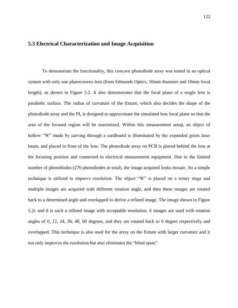
122
5.3 Electrical Characterization and Image Acquisition
To demonstrate the functionality, this concave photodiode array was tested in an optical
system with only one planoconvex lens (from Edmunds Optics, 10mm diameter and 10mm focal
length), as shown in Figure 5.2. It also demonstrates that the focal plane of a single lens is
parabolic surface. The radius of curvature of the fixture, which also decides the shape of the
photodiode array and the PI, is designed to approximate the simulated lens focal plane so that the
area of the focused region will be maximized. Within this measurement setup, an object of
hollow “W” made by carving through a cardboard is illuminated by the expanded green laser
beam, and placed in front of the lens. The photodiode array on PCB is placed behind the lens at
the focusing position and connected to electrical measurement equipment. Due to the limited
number of photodiodes (276 photodiodes in total), the image acquired looks mosaic. So a simple
technique is utilized to improve resolution. The object “W” is placed on a rotary stage and
multiple images are acquired with different rotation angle, and then these images are rotated
back to a determined angle and overlapped to derive a refined image. The image shown in Figure
5.2c and d is such a refined image with acceptable resolution. 6 images are used with rotation
angles of 0, 12, 24, 36, 48, 60 degrees, and they are rotated back to 0 degree respectively and
overlapped. This technique is also used for the array on the fixture with larger curvature and it
not only improves the resolution but also eliminates the “blind spots”.

123
Figure 5.2 (a) shows the optical setup for image creation (b) shows the convave photo detector
array (c) and (d) show the collected image using Labview and Matlab to extract and process the
collected IV data from the pixels.
5.4 Summary
In conclusion, we demonstrate the procedure to fabricate photodiode array on concave
curvilinear surface and verify its functionality within a single-lens image system that has
practical applications such as endoscope. This procedure is compatible with planar
semiconductor fabrication techniques, so that not only photodiodes but all other semiconductor
devices, such as MOSFETs, BJTs, LEDs, etc, are available to integrate onto curvilinear surfaces.

124
On the other hand, little requirement is imposed on the curvature of the surface since imaging
techniques are available to eliminates “blind spots” and improves resolution. With these merits
of this procedure, an artificial eye device with similar size of human eye is realizable with a
tunable lens and controllable fixture. Generally, this procedure enlarges the device design
freedom and will make numerous ideas practical in various areas.

125
Chapter 6 Conclusion and Future Work
6.1 Conclusions
In this these three main topics were covered the first was graphene syntheses and the
applications the material can be used in. Some of which include transparent electrodes, bang gap
modification in bilayer graphene, and transistor devices. As the processing challenges of current
silicon technology continues alternative like graphene will have to be considered to continue
gaining performance enhancements and lower power operation. Besides this the application of
transparent electrodes allows for graphene to be used in another unrelated area giving it the
opportunity to expand beyond the device section and into the energy harvesting and display
technologies. The next material was diamond this material has the potential to change the
capabilities of next generation power electronic devices. As the proliferation of electric vehicles
increases and the development of a new generation of nuclear reactor starts materials that have
properties that are sutitable for multiple fields are become very attractive. Current growth
technology has found ways to grow diamond in large quantities and with a variety of doping
concentrations for use in a variety of application ranging from temperature sensors to high power
rectifiers. As the demands on current wide bandgap materials continues alternative like diamond
will continue to gain popularity and find its place in the family of useful semiconductors.
6.2 Future Work
Future work will include developing additional straining techniques for graphene and
other two dimensional films. The development of controllable strain will allow for materials like
bilayer graphene to begin being using for active electronic devices. The main challenge will be

126
ensuring that the band gaps remain uniform in time and throughout the surfaces to ensure
consistent device performance. Additional project will be creating optoelectronic devices that
can utilize the unique optical and electronic properties of graphene on the FIR and terahertz
regimes.
Future work for diamond devices will include developing high power transistors using
the PECVD doped diamond samples. In the coming years as the world looks to green energy to
replace traditional coal and natural gas nuclear energy is an ideal candidate. New reactors are
being designed with more safety features and smaller in size. One issue is developing a new
generation of monitoring tools to accommodate the new reactors different and new operating
regimes. Sensors made of synthetic diamond can be used for countaig high energy particles as
well as creating diodes for use as temperature sensors Beyond the radiation environment
diamond host of promising properties make diamond an ideal material for many high
performance applications. The future demand and the ease of growth of diamond make the future
of diamond very promising.
6.3 References
1. Freitag, M., Graphene: Trilayers unravelled. Nature Physics, 2011. 7(8): p. 596-597.
2. Rao, C.N.R. and A.K. Sood, Graphene: synthesis, properties, and phenomena. 2013:
John Wiley & Sons.
3. Henriksen, E., et al., Cyclotron resonance in bilayer graphene. Physical review letters,
2008. 100(8): p. 087403.

127
4. Zhang, Y., et al., Direct observation of a widely tunable bandgap in bilayer graphene.
nature, 2009. 459(7248): p. 820-823.
5. Choi, S.-M., S.-H. Jhi, and Y.-W. Son, Controlling energy gap of bilayer graphene by
strain. Nano letters, 2010. 10(9): p. 3486-3489.
6. Verberck, B., et al., Strain-induced band gaps in bilayer graphene. Physical Review B,
2012. 85(12): p. 125403.
7. Spieler, H., Radiation detectors and signal processing. Introduction: Vertex Detection in
High Energy Physics.-2001, Univ. Heidelberg, 2001: p. 28-34.
8. Willatzen, M., M. Cardona, and N. Christensen, Linear muffin-tin-orbital and k⋅ p
calculations of effective masses and band structure of semiconducting diamond. Physical
Review B, 1994. 50(24): p. 18054.
9. Neves, A. and M.H. Nazaré, Properties, growth and applications of diamond. 2001: IET.
10. Massarani, B., J. Bourgoin, and R. Chrenko, Hopping conduction in semiconducting
diamond. Physical Review B, 1978. 17(4): p. 1758.
11. Bundy, F.P., The P, T phase and reaction diagram for elemental carbon, 1979. Journal of
Geophysical Research: Solid Earth (1978–2012), 1980. 85(B12): p. 6930-6936.
12. Mankelevich, Y.A. and P. May, New insights into the mechanism of CVD diamond
growth: Single crystal diamond in MW PECVD reactors. Diamond and Related
Materials, 2008. 17(7): p. 1021-1028.
13. Evans, T. and P. James. A study of the transformation of diamond to graphite. in
Proceedings of the Royal Society of London A: Mathematical, Physical and Engineering
Sciences. 1964: The Royal Society.
128
14. Ellinger, F., et al. Review of advanced and beyond CMOS FET technologies for radio
frequency circuit design. in Microwave & Optoelectronics Conference (IMOC), 2011
SBMO/IEEE MTT-S International. 2011: IEEE.
15. Novoselov, K.S., et al., Electric field effect in atomically thin carbon films. science, 2004.
306(5696): p. 666-669.
16. Katsnelson, M.I., Graphene: carbon in two dimensions. Materials today, 2007. 10(1): p.
20-27.
17. Aurich, H., J. Trbovic, and C. Schonenberger, Fabrication and Electrical
Characterization of Graphene. 2007, Master thesis by Hagen Aurich University of Basel
Department of Physics.
18. Lee, J., et al., Ab initio study of adsorption properties of hazardous organic molecules on
graphene: Phenol, phenyl azide, and phenylnitrene. Chemical Physics Letters, 2015. 618:
p. 57-62.
19. McCann, E. and M. Koshino, The electronic properties of bilayer graphene. Reports on
Progress in Physics, 2013. 76(5): p. 056503.
20. Neto, A.C., et al., The electronic properties of graphene. Reviews of modern physics,
2009. 81(1): p. 109.
21. Novoselov, K., et al., Two-dimensional gas of massless Dirac fermions in graphene.
nature, 2005. 438(7065): p. 197-200.
22. Zhang, Y., et al., Experimental observation of the quantum Hall effect and Berry's phase
in graphene. nature, 2005. 438(7065): p. 201-204.
23. Bolotin, K.I., et al., Ultrahigh electron mobility in suspended graphene. Solid State
Communications, 2008. 146(9): p. 351-355.

129
24. Du, X., et al., Approaching ballistic transport in suspended graphene. Nature
nanotechnology, 2008. 3(8): p. 491-495.
25. Dean, C., et al., Boron nitride substrates for high-quality graphene electronics. Nature
nanotechnology, 2010. 5(10): p. 722-726.
26. Elias, D., et al., Dirac cones reshaped by interaction effects in suspended graphene.
Nature Physics, 2011. 7(9): p. 701-704.
27. Mayorov, A., et al., Interaction-driven spectrum reconstruction in bilayer graphene.
science, 2011. 333(6044): p. 860-863.
28. Chen, Z., et al., Graphene nano-ribbon electronics. Physica E: Low-dimensional Systems
and Nanostructures, 2007. 40(2): p. 228-232.
29. Han, M.Y., et al., Energy band-gap engineering of graphene nanoribbons. Physical
review letters, 2007. 98(20): p. 206805.
30. Li, X., et al., Chemically derived, ultrasmooth graphene nanoribbon semiconductors.
science, 2008. 319(5867): p. 1229-1232.
31. Wang, X., et al., Room-temperature all-semiconducting sub-10-nm graphene nanoribbon
field-effect transistors. Physical review letters, 2008. 100(20): p. 206803.
32. Ritter, K.A. and J.W. Lyding, The influence of edge structure on the electronic properties
of graphene quantum dots and nanoribbons. Nature materials, 2009. 8(3): p. 235-242.
33. Pedersen, T.G., et al., Graphene antidot lattices: designed defects and spin qubits.
Physical review letters, 2008. 100(13): p. 136804.
34. Bai, J., et al., Graphene nanomesh. Nature nanotechnology, 2010. 5(3): p. 190-194.
35. Yan, J.-A., L. Xian, and M. Chou, Structural and electronic properties of oxidized
graphene. Physical review letters, 2009. 103(8): p. 086802.

130
36. Gilje, S., et al., A chemical route to graphene for device applications. Nano letters, 2007.
7(11): p. 3394-3398.
37. Sofo, J.O., A.S. Chaudhari, and G.D. Barber, Graphane: a two-dimensional
hydrocarbon. Physical Review B, 2007. 75(15): p. 153401.
38. Balog, R., et al., Bandgap opening in graphene induced by patterned hydrogen
adsorption. Nature materials, 2010. 9(4): p. 315-319.
39. Bonaccorso, F., et al., Graphene photonics and optoelectronics. Nature photonics, 2010.
4(9): p. 611-622.
40. Bae, S., et al., Roll-to-roll production of 30-inch graphene films for transparent
electrodes. Nature nanotechnology, 2010. 5(8): p. 574-578.
41. Kim, K.S., et al., Large-scale pattern growth of graphene films for stretchable
transparent electrodes. nature, 2009. 457(7230): p. 706-710.
42. Berciaud, S., et al., Probing the intrinsic properties of exfoliated graphene: Raman
spectroscopy of free-standing monolayers. Nano letters, 2008. 9(1): p. 346-352.
43. Ferrari, A., et al., Raman spectrum of graphene and graphene layers. Physical review
letters, 2006. 97(18): p. 187401.
44. Graf, D., et al., Spatially resolved Raman spectroscopy of single-and few-layer graphene.
Nano letters, 2007. 7(2): p. 238-242.
45. Ferrari, A.C., Raman spectroscopy of graphene and graphite: disorder, electron–phonon
coupling, doping and nonadiabatic effects. Solid State Communications, 2007. 143(1): p.
47-57.
46. Das, A., et al., Monitoring dopants by Raman scattering in an electrochemically top-
gated graphene transistor. Nature nanotechnology, 2008. 3(4): p. 210-215.

131
47. Huang, M., et al., Phonon softening and crystallographic orientation of strained
graphene studied by Raman spectroscopy. Proceedings of the National Academy of
Sciences, 2009. 106(18): p. 7304-7308.
48. Frank, O., et al., Raman 2D-band splitting in graphene: theory and experiment. Acs
Nano, 2011. 5(3): p. 2231-2239.
49. Li, Z., et al., Band structure asymmetry of bilayer graphene revealed by infrared
spectroscopy. Physical review letters, 2009. 102(3): p. 037403.
50. Mak, K.F., et al., Measurement of the optical conductivity of graphene. Physical review
letters, 2008. 101(19): p. 196405.
51. Elias, D., et al., Control of graphene's properties by reversible hydrogenation: evidence
for graphane. science, 2009. 323(5914): p. 610-613.
52. Pereira, V.M., A.C. Neto, and N. Peres, Tight-binding approach to uniaxial strain in
graphene. Physical Review B, 2009. 80(4): p. 045401.
53. McCann, E. and V.I. Fal’ko, Landau-level degeneracy and quantum Hall effect in a
graphite bilayer. Physical review letters, 2006. 96(8): p. 086805.
54. Traversi, F., V. Russo, and R. Sordan, Integrated complementary graphene inverter.
arXiv preprint arXiv:0904.2745, 2009.
55. Li, S.-L., et al., Enhanced logic performance with semiconducting bilayer graphene
channels. Acs Nano, 2010. 5(1): p. 500-506.
56. Li, S.-L., et al., Low operating bias and matched input− output characteristics in
graphene logic inverters. Nano letters, 2010. 10(7): p. 2357-2362.
57. Harada, N., et al., A polarity-controllable graphene inverter. Applied Physics Letters,
2010. 96(1): p. 012102.

132
58. Li, S.L., et al., Complementary‐Like Graphene Logic Gates Controlled by Electrostatic
Doping. Small, 2011. 7(11): p. 1552-1556.
59. Geim, A.K. and K.S. Novoselov, The rise of graphene. Nature materials, 2007. 6(3): p.
183-191.
60. Berger, C., et al., Ultrathin epitaxial graphite: 2D electron gas properties and a route
toward graphene-based nanoelectronics. The Journal of Physical Chemistry B, 2004.
108(52): p. 19912-19916.
61. Berger, C., et al., Electronic confinement and coherence in patterned epitaxial graphene.
science, 2006. 312(5777): p. 1191-1196.
62. Reina, A., et al., Large area, few-layer graphene films on arbitrary substrates by
chemical vapor deposition. Nano letters, 2008. 9(1): p. 30-35.
63. Sutter, P.W., J.-I. Flege, and E.A. Sutter, Epitaxial graphene on ruthenium. Nature
materials, 2008. 7(5): p. 406-411.
64. Coraux, J., et al., Structural coherency of graphene on Ir (111). Nano letters, 2008. 8(2):
p. 565-570.
65. Li, X., et al., Large-area synthesis of high-quality and uniform graphene films on copper
foils. science, 2009. 324(5932): p. 1312-1314.
66. Bhaviripudi, S., et al., Role of kinetic factors in chemical vapor deposition synthesis of
uniform large area graphene using copper catalyst. Nano letters, 2010. 10(10): p. 4128-
4133.
67. Li, X., et al., Graphene films with large domain size by a two-step chemical vapor
deposition process. Nano letters, 2010. 10(11): p. 4328-4334.

133
68. Borgström, M.T., et al., Synergetic nanowire growth. Nature nanotechnology, 2007. 2(9):
p. 541-544.
69. Zhang, W., et al., First-principles thermodynamics of graphene growth on Cu surfaces.
The Journal of Physical Chemistry C, 2011. 115(36): p. 17782-17787.
70. Wu, P., et al., Mechanisms of Graphene Growth on Metal Surfaces: Theoretical
Perspectives. Small, 2014. 10(11): p. 2136-2150.
71. Rodat, S., et al., Kinetic modelling of methane decomposition in a tubular solar reactor.
Chemical Engineering Journal, 2009. 146(1): p. 120-127.
72. Mi, X., et al., Facet-insensitive graphene growth on copper. Physical Review B, 2012.
85(15): p. 155436.
73. Smith, D.L., et al., Mechanism of SiN x H y Deposition from NH 3‐SiH4 Plasma. Journal
of the Electrochemical Society, 1990. 137(2): p. 614-623.
74. Noskov, A., et al., Correlation between stress and structure in chemically vapour
deposited silicon nitride films. Thin Solid Films, 1988. 162: p. 129-143.
75. Lennard-Jones, J., On the forces between atoms and ions. Proceedings of the Royal
Society of London. Series A, Containing Papers of a Mathematical and Physical
Character, 1925: p. 584-597.
76. Liu, Z., et al., Interlayer shear strength of single crystalline graphite. Acta Mechanica
Sinica, 2012. 28(4): p. 978-982.
77. Nagashio, K., et al., Electrical transport properties of graphene on SiO2 with specific
surface structures. Journal of Applied Physics, 2011. 110(2): p. 024513.
78. Cancado, L., et al., Influence of the atomic structure on the Raman spectra of graphite
edges. Physical review letters, 2004. 93(24): p. 247401.

134
79. Casiraghi, C., et al., Raman fingerprint of charged impurities in graphene. Applied
Physics Letters, 2007. 91(23): p. 233108.
80. Balandin, A.A., et al., Superior thermal conductivity of single-layer graphene. Nano
letters, 2008. 8(3): p. 902-907.
81. Mohiuddin, T., et al., Uniaxial strain in graphene by Raman spectroscopy: G peak
splitting, Grüneisen parameters, and sample orientation. Physical Review B, 2009.
79(20): p. 205433.
82. Robinson, J.A., et al., Raman topography and strain uniformity of large-area epitaxial
graphene. Nano letters, 2009. 9(3): p. 964-968.
83. Yoon, D., Y.-W. Son, and H. Cheong, Strain-dependent splitting of the double-resonance
Raman scattering band in graphene. Physical review letters, 2011. 106(15): p. 155502.
84. Grimvall, G., Thermophysical properties of materials. 1999: Elsevier.
85. Frank, O., et al., Compression behavior of single-layer graphenes. Acs Nano, 2010. 4(6):
p. 3131-3138.
86. Pan, W., et al., Biaxial compressive strain engineering in graphene/boron nitride
heterostructures. Scientific reports, 2012. 2.
87. Zabel, J., et al., Raman spectroscopy of graphene and bilayer under biaxial strain:
bubbles and balloons. Nano letters, 2012. 12(2): p. 617-621.
88. Lee, C., et al., Measurement of the elastic properties and intrinsic strength of monolayer
graphene. science, 2008. 321(5887): p. 385-388.
89. Koenig, S.P., et al., Ultrastrong adhesion of graphene membranes. Nature
nanotechnology, 2011. 6(9): p. 543-546.

135
90. Ni, Z.H., et al., Uniaxial strain on graphene: Raman spectroscopy study and band-gap
opening. Acs Nano, 2008. 2(11): p. 2301-2305.
91. Kuzmenko, A., et al., Determination of the gate-tunable band gap and tight-binding
parameters in bilayer graphene using infrared spectroscopy. Physical Review B, 2009.
80(16): p. 165406.
92. Blakslee, O., et al., Elastic constants of compression‐annealed pyrolytic graphite. Journal
of Applied Physics, 1970. 41(8): p. 3373-3382.
93. Ding, X., et al., Measurement of shear strength for HOPG with scanning tunneling
microscopy by thermal excitation method. Ultramicroscopy, 2012. 115: p. 1-6.
94. Guo, Y., W. Guo, and C. Chen, Modifying atomic-scale friction between two graphene
sheets: A molecular-force-field study. Physical Review B, 2007. 76(15): p. 155429.
95. Zhang, L., et al., Determination of the electronic structure of bilayer graphene from
infrared spectroscopy. Physical Review B, 2008. 78(23): p. 235408.
96. Nicol, E. and J. Carbotte, Optical conductivity of bilayer graphene with and without an
asymmetry gap. arXiv preprint arXiv:0801.1836, 2008.
97. Kuzmenko, A., et al., Infrared spectroscopy of electronic bands in bilayer graphene.
Physical Review B, 2009. 79(11): p. 115441.
98. Mathkar, A., et al., Controlled, stepwise reduction and band gap manipulation of
graphene oxide. The Journal of Physical Chemistry Letters, 2012. 3(8): p. 986-991.
99. Ci, L., et al., Atomic layers of hybridized boron nitride and graphene domains. Nature
materials, 2010. 9(5): p. 430-435.
100. Tauc, J., Optical properties and electronic structure of amorphous Ge and Si. Materials
Research Bulletin, 1968. 3(1): p. 37-46.

136
101. Metzger, C., et al., Biaxial strain in graphene adhered to shallow depressions. Nano
letters, 2009. 10(1): p. 6-10.
102. Ding, F., et al., Stretchable graphene: a close look at fundamental parameters through
biaxial straining. Nano letters, 2010. 10(9): p. 3453-3458.
103. Gui, G., et al., Local strain effect on the band gap engineering of graphene by a first-
principles study. Applied Physics Letters, 2015. 106(5): p. 053113.
104. Shioya, H., et al., Straining graphene using thin film shrinkage methods. Nano letters,
2014. 14(3): p. 1158-1163.
105. Carozo, V., et al., Raman signature of graphene superlattices. Nano letters, 2011. 11(11):
p. 4527-4534.
106. Lu, C.-C., et al., Twisting bilayer graphene superlattices. Acs Nano, 2013. 7(3): p. 2587-
2594.
107. Cadelano, E., et al., Nonlinear elasticity of monolayer graphene. Physical review letters,
2009. 102(23): p. 235502.
108. Garaj, S., W. Hubbard, and J. Golovchenko, Graphene synthesis by ion implantation.
Applied Physics Letters, 2010. 97(18): p. 183103.
109. Rius, G., M. Yoshimura, and N. Mestres, Synthesis of patterned nanographene on
insulators from focused ion beam induced deposition of carbon. Journal of Vacuum
Science & Technology B, 2012. 30(3): p. 03D113.
110. Baraton, L., et al., Synthesis of few-layered graphene by ion implantation of carbon in
nickel thin films. Nanotechnology, 2011. 22(8): p. 085601.
111. Gutierrez, G., et al., Multi-layer graphene obtained by high temperature carbon
implantation into nickel films. Carbon, 2014. 66: p. 1-10.

137
112. Mi, H., et al., Creating periodic local strain in monolayer graphene with nanopillars
patterned by self-assembled block copolymer. Applied Physics Letters, 2015. 107(14): p.
143107.
113. Fenno, L., O. Yizhar, and K. Deisseroth, The development and application of
optogenetics. Annual review of neuroscience, 2011. 34: p. 389-412.
114. Thongpang, S., et al., A micro-electrocorticography platform and deployment strategies
for chronic BCI applications. Clinical EEG and neuroscience, 2011. 42(4): p. 259-265.
115. Henle, C., et al., First long term in vivo study on subdurally implanted micro-ECoG
electrodes, manufactured with a novel laser technology. Biomedical microdevices, 2011.
13(1): p. 59-68.
116. Viventi, J., et al., Flexible, foldable, actively multiplexed, high-density electrode array for
mapping brain activity in vivo. Nature neuroscience, 2011. 14(12): p. 1599-1605.
117. Rubehn, B., et al., A MEMS-based flexible multichannel ECoG-electrode array. Journal
of neural engineering, 2009. 6(3): p. 036003.
118. Richner, T.J., et al., Optogenetic micro-electrocorticography for modulating and
localizing cerebral cortex activity. Journal of neural engineering, 2014. 11(1): p. 016010.
119. Schendel, A.A., et al., A cranial window imaging method for monitoring vascular growth
around chronically implanted micro-ECoG devices. Journal of neuroscience methods,
2013. 218(1): p. 121-130.
120. Ledochowitsch, P., et al. A transparent μECoG array for simultaneous recording and
optogenetic stimulation. in Engineering in Medicine and Biology Society, EMBC, 2011
Annual International Conference of the IEEE. 2011: IEEE.

138
121. Minami, T., Substitution of transparent conducting oxide thin films for indium tin oxide
transparent electrode applications. Thin Solid Films, 2008. 516(7): p. 1314-1321.
122. Noh, H.-s., et al., Wafer bonding using microwave heating of parylene intermediate
layers. Journal of micromechanics and microengineering, 2004. 14(4): p. 625.
123. Granqvist, C. and A. Hultåker, Transparent and conducting ITO films: new developments
and applications. Thin Solid Films, 2002. 411(1): p. 1-5.
124. Guillen, C. and J. Herrero, Comparison study of ITO thin films deposited by sputtering at
room temperature onto polymer and glass substrates. Thin Solid Films, 2005. 480: p.
129-132.
125. Li, X., et al., Transfer of large-area graphene films for high-performance transparent
conductive electrodes. Nano letters, 2009. 9(12): p. 4359-4363.
126. Chen, H., et al., Mechanically strong, electrically conductive, and biocompatible
graphene paper. Adv. Mater, 2008. 20(18): p. 3557-3561.
127. Li, N., et al., The promotion of neurite sprouting and outgrowth of mouse hippocampal
cells in culture by graphene substrates. Biomaterials, 2011. 32(35): p. 9374-9382.
128. Williams, J.C., et al., Complex impedance spectroscopy for monitoring tissue responses
to inserted neural implants. Journal of neural engineering, 2007. 4(4): p. 410.
129. Norlin, P., et al., A 32-site neural recording probe fabricated by DRIE of SOI substrates.
Journal of micromechanics and microengineering, 2002. 12(4): p. 414.
130. Gross, G.W., Simultaneous single unit recording in vitro with a photoetched laser
deinsulated gold multimicroelectrode surface. Biomedical Engineering, IEEE
Transactions on, 1979(5): p. 273-279.

139
131. Yuen, T. and W. Agnew, Histological evaluation of polyesterimide-insulated gold wires
in brain. Biomaterials, 1995. 16(12): p. 951-956.
132. Zhang, N., et al., Temperature sensor based on 4H-silicon carbide pn diode operational
from 20 C to 600 C. Applied Physics Letters, 2014. 104(7): p. 073504.
133. Meier, D., CVD diamond sensors for particle detection and tracking. 1999, CERN
Geneva (Switzerland).
134. Kittel, C., Introduction to solid state physics. 2005: Wiley.
135. Alianelli, L., et al., A planar refractive x-ray lens made of nanocrystalline diamond.
Journal of Applied Physics, 2010. 108(12): p. 123107.
136. Mildren, R. and A. Sabella, Highly efficient diamond Raman laser. Optics letters, 2009.
34(18): p. 2811-2813.
137. May, P.W., Diamond thin films: a 21st-century material. Philosophical Transactions of
the Royal Society of London A: Mathematical, Physical and Engineering Sciences, 2000.
358(1766): p. 473-495.
138. Porro, S., et al., Nanocrystalline diamond coating of fusion plasma facing components.
Diamond and Related Materials, 2009. 18(5): p. 740-744.
139. Nebel, C.E., et al., Diamond for bio-sensor applications. Journal of Physics D: Applied
Physics, 2007. 40(20): p. 6443.
140. Bergonzo, P., et al., 3D shaped mechanically flexible diamond microelectrode arrays for
eye implant applications: The MEDINAS project. Irbm, 2011. 32(2): p. 91-94.
141. Clark, C., P. Dean, and P. Harris. Intrinsic edge absorption in diamond. in Proceedings of
the Royal Society of London A: Mathematical, Physical and Engineering Sciences. 1964:
The Royal Society.

140
142. Sokoloff, J., Electron localization in crystals with quasiperiodic lattice potentials.
Physical Review B, 1980. 22(12): p. 5823.
143. Calzaferri, G. and R. Rytz, The band structure of diamond. The Journal of Physical
Chemistry, 1996. 100(26): p. 11122-11124.
144. Thonke, K., The boron acceptor in diamond. Semiconductor science and technology,
2003. 18(3): p. S20.
145. Inushima, T., et al., Hopping conduction via the excited states of boron in p-type
diamond. Diamond and Related Materials, 2000. 9(3): p. 1066-1070.
146. Bovenkerk, H., et al., Preparation of diamond. 1959.
147. Ece, M., B. Oral, and J. Patscheider, Nucleation and growth of diamond films on Mo and
Cu substrates. Diamond and Related Materials, 1996. 5(3): p. 211-216.
148. Yamada, H., et al., Numerical analyses of a microwave plasma chemical vapor
deposition reactor for thick diamond syntheses. Diamond and Related Materials, 2006.
15(9): p. 1389-1394.
149. Watanabe, H., et al., Homoepitaxial diamond film with an atomically flat surface over a
large area. Diamond and Related Materials, 1999. 8(7): p. 1272-1276.
150. Okushi, H., et al., Device-grade homoepitaxial diamond film growth. Journal of crystal
growth, 2002. 237: p. 1269-1276.
151. Bachmann, P.K., D. Leers, and D.U. Wiechert, Diamond Thin Films: Preparation,
Characterization and Selected Applications Progress Report. Berichte der
Bunsengesellschaft für physikalische Chemie, 1991. 95(11): p. 1390-1400.
152. Goodwin, D., et al., Handbook of industrial diamonds and diamond films. editor Prelas
MA, New York, Dekker, 1998.

141
153. Mermoux, M., et al., Raman characterization of boron-doped 111 homoepitaxial
diamond layers. Diamond and Related Materials, 2006. 15(4): p. 572-576.
154. Maeta, H., et al., The characterization of synthetic and natural single crystal diamonds by
x-ray diffraction. Physica B: Condensed Matter, 2006. 376: p. 283-287.
155. Hayashi, K., et al., Investigation of the effect of hydrogen on electrical and optical
properties in chemical vapor deposited on homoepitaxial diamond films. Journal of
Applied Physics, 1997. 81(2): p. 744-753.
156. Yamanaka, S., et al., Electrical conduction of high-conductivity layers near the surfaces
in hydrogenated homoepitaxial diamond films. Applied surface science, 2000. 159: p.
567-571.
157. Tsubota, T., et al., Surface morphology and electrical properties of boron-doped diamond
films synthesized by microwave-assisted chemical vapor deposition using trimethylboron
on diamond (100) substrate. Diamond and Related Materials, 2000. 9(7): p. 1362-1368.
158. Tokuda, N., et al., Hillock-free heavily boron-doped homoepitaxial diamond films on
misoriented (001) substrates. Japanese journal of applied physics, 2007. 46(4R): p. 1469.
159. Takeuchi, D., et al., Device Grade B‐Doped Homoepitaxial Diamond Thin Films. physica
status solidi (a), 2001. 186(2): p. 269-280.
160. Takeuchi, D., et al., High quality homoepitaxial diamond thin film synthesis with high
growth rate by a two-step growth method. Diamond and Related Materials, 1999. 8(6): p.
1046-1049.
161. Tallaire, A., et al., Growth of large size diamond single crystals by plasma assisted
chemical vapour deposition: Recent achievements and remaining challenges. Comptes
Rendus Physique, 2013. 14(2): p. 169-184.

142
162. Issaoui, R., et al., Evaluation of freestanding boron-doped diamond grown by chemical
vapour deposition as substrates for vertical power electronic devices. Applied Physics
Letters, 2012. 100(12): p. 122109.
163. Field, J.E., The properties of natural and synthetic diamond. 1992: Academic Press
London.
164. Thongnopkun, P. and S. Ekgasit, FTIR Spectra of faceted diamonds and diamond
simulants. Diamond and Related Materials, 2005. 14(10): p. 1592-1599.
165. Jenkins, A.L. and R.A. Larsen, Gemstone identification using Raman spectroscopy.
disclosure, 2004. 7: p. 9.
166. Iakoubovskii, K. and G. Adriaenssens, Optical characterization of natural Argyle
diamonds. Diamond and Related Materials, 2002. 11(1): p. 125-131.
167. Issaoui, R., et al., Growth of thick heavily boron-doped diamond single crystals: Effect of
microwave power density. Applied Physics Letters, 2010. 97(18): p. 182101.
168. Tsubota, M., et al., High-temperature characteristics of charge collection efficiency using
single CVD diamond detectors. Nuclear Instruments and Methods in Physics Research
Section A: Accelerators, Spectrometers, Detectors and Associated Equipment, 2015. 789:
p. 50-56.
169. Atchison, D.A. and G. Smith, Optics of the human eye. 2000.
170. Sze, S.M. and K.K. Ng, Physics of semiconductor devices. 2006: John Wiley & Sons.
171. Chen, W.-K., VLSI technology. Vol. 8. 2003: CRC Press.
172. Rim, S.-B., et al., The optical advantages of curved focal plane arrays. Opt. Express,
2008. 16(7): p. 4965-4971.

143
173. Kim, D.-H., et al., Stretchable and foldable silicon integrated circuits. science, 2008.
320(5875): p. 507-511.
174. Kim, D.H. and J.A. Rogers, Stretchable electronics: materials strategies and devices.
Advanced Materials, 2008. 20(24): p. 4887-4892.
175. Yuan, H.-C., et al., Flexible photodetectors on plastic substrates by use of printing
transferred single-crystal germanium membranes. Applied Physics Letters, 2009. 94(1):
p. 13102.
176. Ko, H.C., et al., A hemispherical electronic eye camera based on compressible silicon
optoelectronics. nature, 2008. 454(7205): p. 748-753.
177. Jung, I., et al., Paraboloid electronic eye cameras using deformable arrays of
photodetectors in hexagonal mesh layouts. Applied Physics Letters, 2010. 96(2): p.
021110.
178. Jeong, K.-H., J. Kim, and L.P. Lee, Biologically inspired artificial compound eyes.
science, 2006. 312(5773): p. 557-561.
179. Lee, L.P. and R. Szema, Inspirations from biological optics for advanced photonic
systems. science, 2005. 310(5751): p. 1148-1150.
180. Mannsfeld, S.C., et al., Highly sensitive flexible pressure sensors with microstructured
rubber dielectric layers. Nature materials, 2010. 9(10): p. 859-864.
181. Takei, K., et al., Nanowire active-matrix circuitry for low-voltage macroscale artificial
skin. Nature materials, 2010. 9(10): p. 821-826.
182. Chen, W.-K., VLSI technology 2003: CRC Press.

144
183. Heung Cho, K., et al., A hemispherical electronic eye camera based on compressible
silicon optoelectronics. Nature, 2008. 454(Copyright 2008, The Institution of
Engineering and Technology): p. 748-53.
184. Dinyari, R., et al., Curving monolithic silicon for nonplanar focal plane array
applications. Applied Physics Letters, 2008. 92(9): p. 091114-3.
185. Jin, H.-C., et al., Soft lithographic fabrication of an image sensor array on a curved
substrate. Journal of Vacuum Science & Technology B: Microelectronics and Nanometer
Structures, 2004. 22(5): p. 2548-2551.
186. Jeong, K.-H., J. Kim, and L.P. Lee, Biologically inspired artificial compound eyes.
Science, 2006. 312(Compendex): p. 557-561.