carbon defects as sources of the green and yellow
TRANSCRIPT

PHYSICAL REVIEW B 90, 235203 (2014)
Carbon defects as sources of the green and yellow luminescence bands in undoped GaN
M. A. Reshchikov* and D. O. DemchenkoDepartment of Physics, Virginia Commonwealth University, Richmond, Virginia 23284, USA
A. UsikovNitride Crystals, Inc., 181 East Industry Court, Suite B, Deer Park, New York 11729, USA
and Saint-Petersburg National Research University of Information Technologies, Mechanics and Optics, Saint Petersburg, 197101, RussianFederation
H. Helava and Yu. MakarovNitride Crystals, Inc., 181 East Industry Court, Suite B, Deer Park, New York 11729, USA
(Received 30 June 2014; revised manuscript received 4 November 2014; published 12 December 2014)
In high-purity GaN grown by hydride vapor phase epitaxy, the commonly observed yellow luminescence (YL)band gives way to a green luminescence (GL) band at high excitation intensity. We propose that the GL bandwith a maximum at 2.4 eV is caused by transitions of electrons from the conduction band to the 0/+ level of theisolated CN defect. The YL band, related to transitions via the −/0 level of the same defect, has a maximum at2.1 eV and can be observed only for some high-purity samples. However, in less pure GaN samples, where noGL band is observed, another YL band with a maximum at 2.2 eV dominates the photoluminescence spectrum.The latter is attributed to the CNON complex.
DOI: 10.1103/PhysRevB.90.235203 PACS number(s): 78.55.Cr, 71.55.Eq, 61.72.uj, 71.15.Mb
I. INTRODUCTION
Gallium nitride (GaN) is a promising material forhigh-power/high-frequency electronics [1–4]. In particular,thick GaN layers on sapphire substrates and freestanding GaN,grown by hydride vapor phase epitaxy (HVPE), are expectedto have very high breakdown voltage due to a low density ofdefects in this material. In photoluminescence (PL) studies ofhigh-quality freestanding GaN grown by HVPE, the yellowluminescence (YL) band with a maximum at about 2.2 eV andthe green luminescence (GL) band with a maximum at about2.4 eV are the dominant defect-related PL bands [5].Previously, the YL and GL bands were attributed totransitions of electrons from the conduction band to the2−/− and −/0 transition levels, respectively, of the galliumvacancy-oxygen (VGaON) complex [6]. However, accordingto recent calculations using hybrid functionals, the PL bandcaused by transitions of electrons from the conduction band tothe 2−/− level of VGaON is expected to have a maximum at1.4 eV; i.e., in the infrared region [7]. Moreover, the exponen-tial decay of the GL band at low temperatures was explainedwith the assumption that the GL band is caused by transitionsof electrons from an excited state, located very close to theconduction band minimum (CBM), to the −/0 level of theVGaON acceptor [5]. However, such an assumption is not welljustified. Indeed, an excited state close to the conduction bandis possible for a positively charged deep donor, whereas theVGaON acceptor does not have donorlike excited states. Thus,a revision of the attribution for the GL band in GaN is needed.
Published by the American Physical Society under the terms of theCreative Commons Attribution 3.0 License. Further distribution ofthis work must maintain attribution to the author(s) and the publishedarticle’s title, journal citation, and DOI.
Regarding the YL band, two assignments have been re-cently suggested based on modern first-principles calculations.Lyons et al. [8] attributed the YL band to the CN defect,whereas Demchenko et al. [7] proposed that the YL bandis caused by the CNON complex. The CNON complex is a deepdonor with the 0/+ level at 0.75 eV above the valence bandmaximum (VBM). The CN defect in GaN is a deep acceptorwith the −/0 level at 0.9–1.1 eV above the VBM [7,8].The schematic band diagram, including these thermodynamictransition levels, is shown in Fig. 1.
In addition to the acceptor −/0 level of CN, calculationshave predicted the existence of the 0/+ level for this defect at0.43 eV above the VBM [7]. Since the −/0 level of CN andthe 0/+ level of CNON have similar energies, it is possible thatboth the CN and CNON defects produce YL bands with similarshapes and positions (Fig. 1). However, due to the differencein their electronic structure, these defects can be distinguishedthrough the study of the effect of excitation intensity on thePL spectrum. Indeed, it is expected that the CN acceptors inn-type GaN can be saturated with holes (causing saturation ofthe YL band intensity), and at higher excitation intensities thedefects will begin to capture an additional hole. Subsequently,transitions of electrons from the conduction band to the 0/+level of CN will cause a “secondary” PL band, which peaksat higher photon energies (Fig. 1). Lyons et al. [9] calculatedthat optical transitions of electrons from the conduction bandto this level would cause a blue band with a maximum atabout 2.7 eV. These authors noticed that in C-doped GaN, ablue band is often observed when the carbon concentrationis high [10,11], or at high excitation intensity [12,13], which,in their opinion, supported the existence of the 0/+ level ofthe CN defect. In contrast, there is only one optically activetransition level for the CNON complex in the band gap of GaN.A second level, +/2+ is predicted to be very close to thevalence band (Fig. 1) and will act as a repulsive center forholes. Therefore, the saturation of the CNON-related YL bandwill not be followed by the emergence of another PL band
1098-0121/2014/90(23)/235203(16) 235203-1 Published by the American Physical Society

RESHCHIKOV, DEMCHENKO, USIKOV, HELAVA, AND MAKAROV PHYSICAL REVIEW B 90, 235203 (2014)
FIG. 1. (Color online) Schematic band diagram and predictedtransition levels for the CNON complex and the isolated CN defect.Calculations predict that the CNON complex forms the 0/+ transitionlevel in the band gap, while CN forms two transition levels: (−/0 and0/+. The CNON complex is expected to generate only the YL band.The CN defect can generate the YL band and an additional, higherenergy band after the YL is saturated.
at higher photon energies. This important distinction betweenthe two defects should allow reliable attribution of the YLband to either CN or CNON, depending on the existence of thesecondary band.
In this paper, we investigated the PL behavior for a numberof GaN samples. We arrived at the conclusion that the GL bandwith a maximum at 2.4 eV, and not the blue band, is causedby electron transitions via the 0/+ level of the CN defect. ThePL bands associated with the CN and CNON defects can bothbe called YL bands since they have only slightly differentpositions of their maxima. It appears that in a majority of GaNsamples, the CNON complex is responsible for the YL band.The CN defect can be revealed through the observation of thesecondary (GL) band only in high-quality GaN grown by theHVPE technique. In this paper, time-resolved PL experimentshave been employed to identify the GL band due to its shortlifetime and exponential decay even at low temperatures(30–100 K).
II. METHODS
A. Experimental details
We observed the GL band (at least in time-resolved PLmeasurements) in more than 20 samples, which were 10-to 30-μm-thick unintentionally doped GaN layers grown byHVPE on c plane, 2 in. sapphire substrates. The growth wasperformed at temperatures of 850–1000 °C, in atmospheric
pressure and in an argon ambient. Ammonia and HCl wereused as the precursors. The growth rate (0.2–1 μm/min) wascontrolled by the HCl gas flow rate through the Ga source.For a more detailed study, two representative samples wereselected: 1007 and RS280. The concentration of free electrons,n, given in Table I for these two samples, is calculated fromthe PL lifetime of the YL band at room temperature, accordingto a model presented in Ref. [14], while the direct Hall effectmeasurements showed an apparent concentration of aboutthree times higher due to the existence of a highly conductivelayer near the GaN/sapphire interface [15].
An additional HVPE-grown sample in this paper was un-doped freestanding GaN produced at the Samsung AdvancedInstitute of Technology (sample B73). The HVPE sampleswere compared to GaN samples grown by metal-organicchemical vapor deposition (MOCVD) on sapphire substrates,in which no traces of the GL band could be found (samplesEM1256, EM6881, EM7169, and EM7049) [16,17].
The concentration of C and O impurities ([C] and [O],respectively) were estimated from secondary ion mass-spectrometry (SIMS) measurements and are given in Table I.The carbon concentration in the MOCVD-grown samples wasvaried in the range of [C] = 4 × 10¹⁶ − 2 × 1017 cm−3 bychanging growth conditions. Samples EM6881, EM7169, andEM7049 are semi-insulating, and only the lower bound fortheir resistivity can be estimated.
Steady-state PL was excited with an unfocused He-Cdlaser (50 mW, 325 nm), dispersed by a 1200 rules/mmgrating in a 0.3 m monochromator and detected by a cooledphotomultiplier tube. Calibrated neutral-density filters wereused to attenuate the excitation power density (P exc) overthe range 10−5–0.2 W/cm2, while a focused beam with adiameter of 0.2 mm was used to obtain P exc up to 100 W/cm2.Time-resolved PL was excited with a nitrogen pulse laser(1 ns pulses, with a repetition rate of 6 Hz, and 337 nmwavelength). The excitation light intensity at the samplesurface, P 0, was varied between 1018 and 1024 cm−2s−1 usingneutral density filters. A closed-cycle optical cryostat was usedfor temperatures between 15 and 320 K. The absolute internalquantum efficiency of PL η is defined as η = I PL/G, whereI PL is the integrated PL intensity from a particular PL bandand G is the concentration of electron-hole pairs created by thelaser per second in the same volume. To find η for a particularPL band, we compared its integrated intensity with the PLintensity obtained from a calibrated GaN sample [18,19]. Allsamples were studied under identical conditions.
TABLE I. Parameters of GaN samples analyzed in this paper.
Sample Growth Thickness [C] from [O] from n at 300 K ρ at 300 Knumber method (μm) SIMS (cm−3) SIMS (cm−3) (cm−3) (�cm)
1007 HVPE 22 7 × 10¹⁶ 1 × 10¹⁷ 6 × 10¹⁶ ∼0.1RS280 HVPE 27 0.5 × 10¹⁶ 6 × 10¹⁶ 2 × 10¹⁶ ∼0.1B73 HVPE 200 ∼1 × 10¹⁶ ∼2 × 10¹⁶ 1.3 × 10¹⁶ 0.4EM1256 MOCVD 2.2 4 × 10¹⁶ 5 × 10¹⁶ 2 × 10¹⁶ 0.6EM6881 MOCVD 3.2 7 × 10¹⁶ 5 × 10¹⁶ − >1011
EM7169 MOCVD 2.5 1 × 10¹⁷ 6 × 10¹⁶ − >1011
EM7049 MOCVD 1.9 2 × 10¹⁷ 5 × 10¹⁶ − >1011
235203-2

CARBON DEFECTS AS SOURCES OF THE GREEN AND . . . PHYSICAL REVIEW B 90, 235203 (2014)
B. Theoretical details
To find the transition levels for the CN and CNON defects, weperformed Heyd-Scuseria-Ernzerhof (HSE) hybrid functional[20] calculations. As in a previous paper [7], we adjustedthe fraction of exact exchange to 0.312 and the screening
parameter to 0.2 A−1
. The computed band gap of 3.50 eVagrees with the low-temperature experimental value of 3.50 eV,and the computed relaxed lattice parameters for wurtzite GaN(a = 3.210 A, c = 5.198 A, and u = 0.377) also agree withthe experimental values (a = 3.189 A and c = 5.185 A) [21].The 128 atom supercells were used with all internal degrees offreedom relaxed using HSE hybrid functional calculations toresult in forces of 0.05 eV/A or less. The plane-wave basis setswith a 400 eV cutoff at the � point were used in all calculations.Spin-polarized calculations were performed in all cases. Thedetails of the calculation methods and corrections to defectenergies can be found in Ref. [7].
It is necessary to mention a practical issue regarding thepotential alignment �V correction, which originates fromdropping the diverging G = 0 term in the Fourier energyexpansion in a charged supercell [22]. This correction is rela-tively small (0.05 to 0.1 eV) and is proportional to the defectcharge. In this paper, we compared the results of calculationswith experimental measurements and analyzed the effect thiscorrection has on the computed properties of different types ofdefects (e.g., isolated defects vs complexes). Although thereare no significant changes to the final results, it appears thatthe potential alignment corrections slightly worsen the resultsfor the isolated defect CN, but slightly improve the resultsfor CNON complex. This may indicate that isolated defectsand defect complexes have different electric dipole properties.Therefore, different corrections accounting for the artificialdipole interactions in periodic supercells may have to beapplied for the two types of defects. In this study, �V wasapplied only to the CNON complex, which improved the resultsby up to 0.1 eV. Further study is needed to clarify this behavior.
III. RESULTS
A. Yellow and blue luminescence bandsin GaN grown by MOCVD
The YL band in GaN grown by MOCVD has a maximumat 2.2 eV (Figs. 2 and 3). In conductive n-type GaN (sampleEM1256), the YL band intensity begins to saturate at excitationintensities Pexc > 10−5 W/cm2 (Fig. 2). The shape of the YLband I PL(�ω) and position of its maximum �ωmax remainedunchanged for excitation intensities up to 0.2 W/cm2. Theshape of the YL band at low temperature can be modeledwith the following formula derived from a one-dimensionalconfiguration coordinate model [23]
I PL(�ω) ∝ exp
[−2Se
(√E0 + 0.5�� − �ω
E0 + 0.5�� − �ωmax− 1
)2],
(1)
where Se and �� are the Huang-Rhys factor and the dominantphonon energy for the excited state, �ω is the photon energy,and E0 is the zero-phonon line (ZPL) energy. The values of ��,E0, and �ωmax (52 meV, 2.64 eV, and 2.20 eV, respectively)
FIG. 2. (Color online) Low-temperature PL spectra from con-ductive n-type GaN grown by MOCVD (sample EM1256). The PLintensity is divided by the excitation intensity. The thick solid line 1is calculated using Eq. (1) with the following parameters: Se = 7.4;E0 = 2.64 eV; �ωmax = 2.20 eV; and �� = 52 meV.
are typical for the YL band in GaN [5]. Note that no other lu-minescence bands can be found in the range from 2.6 to 3.2 eVfor the sample with a low concentration of carbon (Fig. 2).
For semi-insulating GaN, a broad band can be found in theblue spectral region only in some samples (Fig. 3) [16]. Theband has a maximum at 3.03 eV and is identified as the BL2band, sometimes observed in high-resistivity GaN grown byMOCVD [24,25]. It has a characteristic fine structure, withthe ZPL at 3.333 eV (inset in Fig. 3). In the past, the BL2
FIG. 3. (Color online) Low-temperature PL spectra at Pexc =10−4 W/cm2 from semi-insulating GaN samples grown by MOCVD.The PL intensity is divided by the excitation intensity. The concen-tration of carbon [C] is given in units of 1017 cm−3. The inset showsa high resolution of the region near the ZPL of the BL2 band.
235203-3

RESHCHIKOV, DEMCHENKO, USIKOV, HELAVA, AND MAKAROV PHYSICAL REVIEW B 90, 235203 (2014)
band has been attributed to transitions of electrons from theconduction band (or from a state very close to the conductionband) to a defect level located at 0.15 eV above the VBM [24].An important feature of the BL2 band is that it bleaches duringcontinuous ultraviolet (UV) illumination, indicating unstablebehavior [25]. It was suggested previously that the BL2 bandis associated with some defect complex containing hydrogen,and the bleaching is caused by dissociation of this complexunder UV exposure [5,25]. It is unclear why the BL2 band ispresent only in some semi-insulating GaN samples and cannotbe found in others (Fig. 3) and why the YL intensity variesconsiderably in different samples. Further studies are neededto clarify this issue.
Another blue band (labeled BL) peaking at 2.9 eV (notshown here), which is related to the ZnGa acceptor, can beobserved in semi-insulating GaN, when the BL2 band isquenched and disappears at temperatures above 150 K [25].Both the BL and BL2 bands apparently have no relation tothe isolated CN defect. On the other hand, the GL band with amaximum at 2.4 eV is a good candidate for transitions via the0/+ level of the CN defect, as will be discussed below.
B. Green luminescence band in freestanding GaN
1. Shape of the GL band
The GL band with a maximum at about 2.4 eV appearsunder high excitation intensity in the steady-state PL spectrumof high-quality GaN samples grown by the HVPE method.The nearly quadratic dependence of the GL intensity on Pexc
in n-type GaN is a strong indication that the defect respon-sible for this band captures two holes before any radiativerecombination takes place [6]. However, it is often difficultto resolve the GL band in steady-state PL spectra, because itusually overlaps with the YL band at room temperature andwith the UV luminescence (UVL) band or BL band at lowtemperatures. In this paper, we extracted the shape of the GLband from time-resolved PL measurements, because in theseexperiments the GL band can be isolated due to its PL lifetimebeing significantly shorter than that for other defect-relatedPL bands [26]. Figure 4 shows the PL spectrum taken 1 μsafter pulsed excitation at various temperatures. The GL bandhas a maximum at 2.40 eV and a full width at half-maximum(FWHM) of 0.43 eV at low temperatures. For a very widerange of PL intensities (almost three orders of magnitude), theshape of the GL band can be fit with Eq. (1), as shown in Fig. 4.The PL band shape remains unchanged for different excitationintensities and for different time delays.
At temperatures below 100 K, the shape of the GL band isasymmetric, as is typically observed for defects with moderateelectron-phonon coupling. By employing a one-dimensionalconfiguration-coordinate model [5,27], we have estimated theenergy of the dominant phonon mode in the excited stateas �� = 41 ± 5 meV from the analysis of the temperaturedependence of the GL band FWHM as the temperature wasincreased from 30 to 300 K. Other parameters in Eq. (1) forthe GL band were estimated as Se = 8.5, E0 = 2.9 eV, and�ωmax = 2.4 eV from the best fit with the experimental data atT = 30 and 100 K (Fig. 4). The above-determined parameters,which describe the shapes and positions of the YL and GLbands, will be used in the following sections to simulate the
FIG. 4. (Color online) Normalized PL spectra at 10−6 s after alaser pulse with P0 = 5 × 1023 cm−2s−1 from freestanding GaN(sample B73). The symbols are experimental points, and the solidcurve is calculated using Eq. (1) with the following parameters:Se = 8.5; E0 = 2.9; �ωmax = 2.4 eV; and �� = 41 meV.
shapes of the YL and GL bands and to resolve them in those PLspectra where they overlap with each other and other PL bands.
2. Effect of temperature
While the PL from freestanding GaN containing the GLband has been previously studied at temperatures below 300 K[5], we are not aware of any reports on its behavior for highertemperatures. Figure 5 shows the PL spectra from sampleB73 for select temperatures. At 300 K, a broad band witha maximum at 2.37 eV consists of two overlapping YL and
FIG. 5. (Color online) PL spectra at selected temperatures forsample B73. The lines show steady-state PL spectra at Pexc =0.3 W/cm2. Triangles show time-resolved PL spectrum measuredat 300 K.
235203-4

CARBON DEFECTS AS SOURCES OF THE GREEN AND . . . PHYSICAL REVIEW B 90, 235203 (2014)
FIG. 6. (Color online) Temperature dependence of the GL bandintensity and the GL lifetime for sample B73. The solid lineis calculated using Eq. (2) for PL intensity and Eq. (3) for PLlifetime with the following parameters: η0 = 0.1; Cp = 10−6 cm3/s;τ0 = 40 μs; EA = 535 meV; Nv = 3.2 × 10¹⁵ T 3/2 cm−3; and g = 2.
GL bands. The comparison of the steady-state PL spectrumwith the time-resolved PL spectrum for the GL band (shownwith triangles in Fig. 5) indicates that the contribution fromthe YL band in the steady-state PL spectrum is small at 300 K(the YL band is not present in the time-resolved PL spectrumdue to its long lifetime). The deconvolution of the broad bandinto the YL and GL bands with known shapes (not shown inFig. 5) indicates that, as the temperature is increased from 300to 380 K, the YL band intensity is nearly constant, whereasthe intensity of the GL band decreases and it finally disappearsat T ≈ 400 K. At temperatures between 380 and 560 K, thedefect-related PL band maximum gradually shifts from 2.10to 1.93 eV. It is not clear whether the broad, red-yellow bandconsists of two bands associated with two different defects, orif the band is related to a single defect and the band redshiftsdue to the decreasing band gap with increasing temperature.The near-band-edge (NBE) peak shifts from 3.37 to 3.27 eVas the temperature is increased from 380 to 560 K.
The temperature dependences of the GL band intensity andthe GL lifetime are shown in Fig. 6. The dependences arevery similar to each other and can be fit with the followingexpressions [14]
I PL(T ) = I0
1 + (1 − η0)τ0CpNvg−1 exp(−EA/kT ), (2)
τ (T ) = τ0
1 + (1 − η0)τ0CpNvg−1 exp(−EA/kT ), (3)
where I 0, η0, and τ0 are the PL intensity, quantum efficiency,and PL lifetime, respectively, for the GL band before PLquenching begins (at about 290 K), Cp is the hole-capturecoefficient for the defect state responsible for the GL band,Nv is the effective density of states in the valence band, EA
is the energy distance between the VBM and the defect stateresponsible for the GL band, and g is its degeneracy. From the
fit, shown with a solid line in Fig. 6, we have estimated thatEA ≈ 0.54 eV and Cp ≈ 10−6 cm3/s.
C. Yellow and green luminescence bands in GaNlayers grown by HVPE
Detailed studies of the effect of excitation intensity on PLwere conducted at T = 100 K. This temperature was chosenbecause at lower temperatures, the exciton emission is verystrong and may contribute as a parasitic signal at photonenergies where the defect-related bands were observed. Onthe other hand, the temperature-induced broadening of theGL band can be ignored at 100 K, as can be seen in Fig. 4.The contribution of the GL band in the PL spectrum and itsPL lifetime varied from sample to sample, apparently due todifferent concentrations of point defects and free electrons inthe set of 20 undoped GaN samples (layers on sapphire) grownby HVPE.
Below, the results are presented for two representativesamples: a high-purity sample with the strongest GL band(sample RS280) and a less pure sample in which the YLband was stronger and the GL band could be observedonly in time-resolved PL measurements (sample 1007). Toevaluate the presence of carbon, oxygen, and a few otherimpurities, dedicated SIMS measurements for samples RS280and 1007 have been carried out by the Evans AnalyticalGroup. In this analysis, a very low detection limit for carbonwas achieved in vacuum by removing carbon adsorbed atthe surface. The reduction in surface carbon resulted in lessinterference (and thus a lower background/detection limit)during the SIMS measurement of the underlying GaN region.The concentrations of selected impurity species in the twosamples are given in Table II. The data for the depths between2 and 4 μm represents the bulk part of the GaN layers. Tocompare with PL results, we will limit the analysis to thedepth range of 100 to 400 nm, because the concentrationof photogenerated charge carriers in our PL experiments isnegligible beyond 400 nm, while the SIMS data in the first100 nm can be affected by impurities absorbed at the surfaceand can be unrealistic.
1. High-purity GaN (strong GL and weak YL)
The steady-state PL spectra for selected excitation intensi-ties and T = 100 K for sample RS280 are shown in Fig. 7.In the PL spectra, the NBE emission has a main peak at3.485 eV and is attributed to the annihilation of free excitons.At low excitation intensities, three defect-related PL bandscan be resolved: the UVL band with a main peak at 3.30 eV,the Zn-related BL band with a maximum at 2.94 eV, and thered luminescence (RL) band with a maximum at 1.82 eV.The RL band in undoped GaN grown by HVPE is preliminarilyattributed to a deep acceptor with an energy level of 1.13 eVabove the valence band [28]. With increasing excitationintensity, the relative contribution of the UVL, BL, and RLbands decreases, and the GL band with a maximum at 2.40 eVemerges (Fig. 7). By subtracting the shapes of the RL andBL bands (obtained from the PL spectrum at the lowestexcitation intensity) from the PL spectrum measured at Pexc =0.2 W/cm2, we obtained a shape of a PL band (the dotted curvein Fig. 7) almost identical to the shape of the GL band found
235203-5

RESHCHIKOV, DEMCHENKO, USIKOV, HELAVA, AND MAKAROV PHYSICAL REVIEW B 90, 235203 (2014)
TABLE II. Concentration of impurities (per cubic centimeter) from SIMS measurements.
RS280 1007
Impurity 100–400 nm 2–4 μm 100–400 nm 2–4 μm Detection limit
C 5.6 × 10¹⁵ 0.4 × 10¹⁵ 8.2 × 10¹⁶ 1.5 × 10¹⁵ 1 × 10¹⁵
O 6.9 × 10¹⁶ 2 × 10¹⁶ 1.3 × 10¹⁷ 6.8 × 10¹⁵ 1 × 10¹⁶
Si 4.9 × 10¹⁵ 2.6 × 10¹⁵ 2.3 × 10¹⁶ 7.6 × 10¹⁶ 8 × 10¹⁵
H 1.6 × 10¹⁷ 1.3 × 10¹⁷ 3.9 × 10¹⁷ 1.3 × 10¹⁷ 2 × 10¹⁷
Cl 3.9 × 10¹⁵ 1.5 × 10¹⁶ 1.7 × 10¹⁶ 1 × 10¹⁷ 1 × 10¹⁵
from the time-resolved PL in freestanding GaN (Fig. 4). Byrepeating this procedure for different excitation intensities, weobtained the dependence of the GL intensity on the excitationintensity (Fig. 8). We can see that at Pexc < 10−3 W/cm2 theGL intensity increases as approximately a square of Pexc.This behavior is expected for optical transitions via the lowertransition level of CN (the 0/+ level) for excitation intensitieswhen the higher transition level (the −/0 level) is not yetsaturated with holes (the YL intensity increases linearly withPexc) [6], because the probability of capturing two holes bya defect before recombination occurs is proportional to thesquare of the excitation intensity. Between 10−3 and 1 W/cm2,the GL band intensity increases linearly with Pexc, because onehole is already bound to the defect and only one additional holeneeds to be captured. The YL band is expected to be saturatedunder these conditions. Finally, at Pexc > 1 W/cm2 the GLband saturates. The saturation of the RL and BL bands beginsat much lower excitation intensities (at Pexc > 10−3 W/cm2).
The solid lines in Fig. 8 are calculated with the followingexpression, which is obtained from rate equations [29,30]
I PL = ηP0 = N
ατln
(1 + ατP0η0
N
). (4)
FIG. 7. (Color online) Steady-state PL spectra for sample RS280at 100 K and selected excitation intensities. The dotted line showsthe PL band obtained as a difference between the PL spectrumat 0.13 mW/cm2 (multiplied by 36) and the PL spectrum at200 mW/cm2. Triangles show the shape of the GL band calculatedusing Eq. (1), with parameters given in Fig. 4.
Here, P 0 is the excitation intensity (expressed as the number ofphotons passing through a unit area of the sample surface perunit time), N is the concentration of defects responsible for aparticular PL band, η0 is the quantum efficiency of that PL bandin the limit of low excitation intensity, and α is the absorptioncoefficient (α ≈ 1.2 × 105 cm−1 for GaN at 3.81 eV [31]). Theonly fitting parameter in Eq. (4) is N . From the best fit, wehave estimated that the concentrations of defects responsiblefor the GL, RL, and BL bands are 1.5 × 10¹⁵, 1.5 × 10¹⁶, and2 × 1015 cm−3, respectively.
The YL band was not observed in the steady-state PLspectra of this sample, because it is obscured by the RL band.
FIG. 8. (Color online) Dependence of the PL intensity on excita-tion intensity for the major PL bands in steady-state PL measurementsfor sample RS280 at 100 K. The experimental points for the GLband are obtained from the PL spectra deconvolution similar to anexample shown in Fig. 7 but use the PL spectrum at lower excitationintensity of 10−5 W/cm2 as the “background” spectrum. The solidlines are calculated using Eq. (4), with the following parameters:η0 = 0.0018; τ0 = 4.5 μs; and N = 1.5 × 1015 cm−3 for the GLband; η0 = 0.025; τ0 = 6 ms; and N = 1.5 × 1016 cm−3 for the RLband; and η0 = 0.035; τ0 = 500 μs; and N = 2 × 1015 cm−3 for theBL band. The dashed line indicates the quadratic dependence of PLintensity on excitation intensity. The dotted line is calculated usingEq. (4), with η0 = 0.0018; τ0 = 2 ms; and N = 1.5 × 1015 cm−3,which is the expected dependence for the YL band.
235203-6

CARBON DEFECTS AS SOURCES OF THE GREEN AND . . . PHYSICAL REVIEW B 90, 235203 (2014)
FIG. 9. (Color online) PL spectra at different time delays afterpulsed excitation with P0 = 5 × 1023 cm−2s−1 for sample RS280.The symbols are experimental points, and the curves are calculatedusing Eq. (1), with the following parameters: Se = 8.5; E0 = 2.9 eV;�ωmax = 2.4 eV; and �� = 41 meV (curves 1 and 2); Se = 7.4;E0 = 2.57 eV; �ωmax = 2.1 eV; and �� = 56 meV (curves 3, 4, and5). The dashed curve 4′ corresponds to the YL band shown in Fig. 12,with Se = 7.4; E0 = 2.64 eV; �ωmax = 2.2 eV; and �� = 56 meV.
To estimate the contribution of the CN-related YL band to thePL spectra at different excitation intensities, we assumed thatthe hole-capture coefficients for the −/0 and 0/+ levels of theCN defect (for the YL and GL bands, respectively) are similar.The expected intensity of the YL band is shown with a dottedcurve in Fig. 8. Note that if the hole capture coefficient for the−/0 level is higher, the intensity of the YL will shift upwardby the same factor. While the YL band with such intensitycould not be observed in the steady-state PL spectrum at anyexcitation intensity, it can be revealed in time-resolved PLmeasurements.
Figure 9 shows the evolution of the PL spectrum for thesame sample after a pulsed excitation at T = 100 K. For shorttime delays (up to 10−5 s), the GL band is the dominant band inthe defect-related part of the spectrum. For longer time delays,the GL band disappears, and the YL band with a maximum at2.1 eV emerges (Fig. 9). The shape of the YL band in Fig. 9is fit using Eq. (1) with the same parameters, �� and Se,as for the YL band in Fig. 2. However, �ωmax = 2.1 eV andE0 = 2.57 eV had to be taken for the best fit in Fig. 9 insteadof 2.2 and 2.64 eV, respectively, which were used in Fig. 2.An example with the latter parameters is shown in Fig. 9 asthe dashed curve 4′. This indicates that these two YL bandsoriginate from two different sources. At longer delay times(longer than 10−3 s), the YL band gradually disappears as itis obscured by the RL band. The BL, GL, YL, and RL bandscan be reliably observed in time-resolved PL spectra becausethey have different PL lifetimes at 100 K: 500 μs (BL band),4.5 μs (GL band), 2 ms (YL band), and ∼6 ms (RL band).
The dependences of the peak intensity on the excitationintensity for the GL, YL, and UVL bands at 100 K are
FIG. 10. (Color online) The dependences of PL intensity after alaser pulse on excitation intensity for PL bands in sample RS280 at100 K. The solid lines are calculated using Eq. (37) of Ref. [30],with the following parameters: η0 = 0.0018; τ0 = 4.5 μs; and N =5 × 1014 cm−3 for the GL band; η0 = 0.0018; τ0 = 2 ms; and N =5 × 1014 cm−3 for the YL band; and η0 = 0.004; τ0 = 100 μs; andN = 5 × 1014 cm−3 for the UVL band. The dashed line indicates thequadratic dependence of PL intensity on the excitation intensity.
shown in Fig. 10. The intensities of the UVL and YL bandsincrease linearly with increasing excitation intensity up to∼1022 cm−2s−1 and saturate at higher excitation intensities.However, the intensity of the GL band increases as a square ofthe excitation intensity for P0 < 1021 cm−2 s−1 (dashed line inFig. 10). These results are consistent with those obtained fromsteady-state PL, suggesting that two holes are captured by thedefect when producing the GL band, while only one hole iscaptured by the same defect when producing the YL band.
2. Less pure GaN (strong YL and weak GL)
Figures 11 and 12 show evolutions of the PL spectra withexcitation intensity (for steady-state PL) and with time (aftera laser pulse) for sample 1007. In steady-state PL spectra, theGL band appears to contribute only at high excitation intensityas a weak shoulder to the stronger YL band. The RL, YL, andGL bands significantly overlap and are difficult to resolve. Todeconvolute the bands, we simulated the shapes of the YL andGL bands by using Eq. (1), with the parameters given in thecaptions of Figs. 2 and 4, respectively, while the shape of theRL band was taken from other samples in which the RL bandwas the dominant defect-related PL band [28]. The intensitiesof the RL band in samples RS280 and 1007 were almost thesame, whereas the YL band was at least an order of magnitudestronger in sample 1007 as compared to sample RS280 (whereit could not be seen in the steady-state PL spectra).
In the PL spectrum obtained after a pulsed excitation, theGL band and the YL band can be clearly seen at short andlong time delays, respectively (Fig. 12). In contrast to sampleRS280 (with �ωmax = 2.1 eV for the YL band), the YL bandhas a maximum at 2.2 eV and the same shape as for GaN
235203-7

RESHCHIKOV, DEMCHENKO, USIKOV, HELAVA, AND MAKAROV PHYSICAL REVIEW B 90, 235203 (2014)
FIG. 11. (Color online) The steady-state PL spectra at T = 18 Kand different excitation intensities for sample 1007. In the defect-related region of the spectra, the contributions from four PL bandscan be found: UVL, GL, YL, and RL. The dashed and dotted curvesshow an example of deconvolution. The crosses show the sum of theGL, YL, and RL bands used for the deconvolution of the PL spectrumat Pexc = 0.19 W/cm2.
samples grown by MOCVD. An example with the parametersof the YL band with �ωmax = 2.1 eV is shown in Fig. 12 asthe dashed curve 2′. The different positions of the YL bandmaxima in time-resolved PL measurements for samples RS280and 1007 are the first indication of the fact that the YL bandsin these two samples are caused by two different defects. Anadditional piece of evidence for this follows from the analysisof the decays of the YL and GL bands after a laser pulse, whichis discussed below.
3. Decay of the GL and YL intensity after a laser pulse
Figure 13 shows the decay of PL intensity at 2.3 eV and100 K after a laser pulse for three HVPE-grown samples.Since the PL intensity integrated over photon energies isnearly the same for the YL and GL bands when theyare normalized at their maxima, and the PL intensities at2.3 eV for the normalized bands are equal (∼85% from theirpeak intensities), the PL intensity at 2.3 eV is proportionalto the number of photons emitted at any time via both theYL and GL mechanisms. Moreover, the relative number ofphotons emitted separately via the YL and GL mechanismscan be found by integrating this intensity over time in the rangeof short time delays (where the GL band dominates and thecontribution of the YL band is negligible) and at longer timedelays (where the GL band vanishes and only the YL bandremains). The dependence of PL intensity on time, I PL(t), canbe fit with the following equation:
I PL(t) = I PL(0) exp (−t/τ ) . (5)
The exponential decay for times shorter than 10−5–10−4 scorresponds to the decay of the GL band with lifetime τ
FIG. 12. (Color online) PL spectra at different time delays aftera pulsed excitation with P0 = 5 × 1021 cm−2s−1 for sample 1007.The symbols are experimental points, and the curves are calculatedusing Eq. (1), with the following parameters: Se = 8.5; E0 = 2.9 eV;�ωmax = 2.4 eV; and �� = 41 meV (curve 1); Se = 7.4; E0 =2.64 eV; �ωmax = 2.2 eV; and �� = 56 meV (curves 2 and 3).The dashed curve 2′ corresponds to the YL band shown in Fig. 9,with Se = 7.4; E0 = 2.57 eV; �ωmax = 2.1 eV; and �� = 56 meV.
ranging from 1.8 to 4.5 μs for different samples. For longertime delays, the nearly exponential decay corresponds to thedecay of the YL band with τ ranging from 0.3 to 1.85 ms.The PL intensities were integrated over time, separately forthe short-living GL and for the long-living YL (inset inFig. 13). The ratio of the GL band intensity to the YL bandintensity in these measurements is 2.4 for sample B73, 1.7 forsample RS280, and 0.18 for sample 1007. Note that thesemeasurements were conducted at high excitation intensity,corresponding to the saturation regime (Fig. 10). If the GL andYL bands in these samples were related to the −/0 and 0/+states of the same defect and if after each pulse, equilibrium inthe dark was completely achieved, then the integrated overtime intensities of the GL and YL bands in time-resolvedmeasurements should be equal. Indeed, when all the CN defectsare saturated with two holes, the same number of photonsshould be emitted from these defects when they lose the firsthole in the process of fast electron-hole recombination (theGL band) and when they subsequently lose the second hole atlonger time delay (the YL band).
The small prevalence of the time-integrated GL intensityover the YL intensity in samples B73 and RS280 can beexplained by incomplete restoration of the dark equilibrium.Such an assumption is supported by the observation of aslower-than-exponential tail of the YL band (Fig. 13). Thismay be due to small contributions from donor-acceptor pair(or shallow donor-deep donor pair) transitions at 100 K, whichpersist for a long time [32]. Since the restoration appears tobe incomplete (the next pulse arrives before all the defectsbecome completely filled with electrons), the integrated over
235203-8
CARBON DEFECTS AS SOURCES OF THE GREEN AND . . . PHYSICAL REVIEW B 90, 235203 (2014)
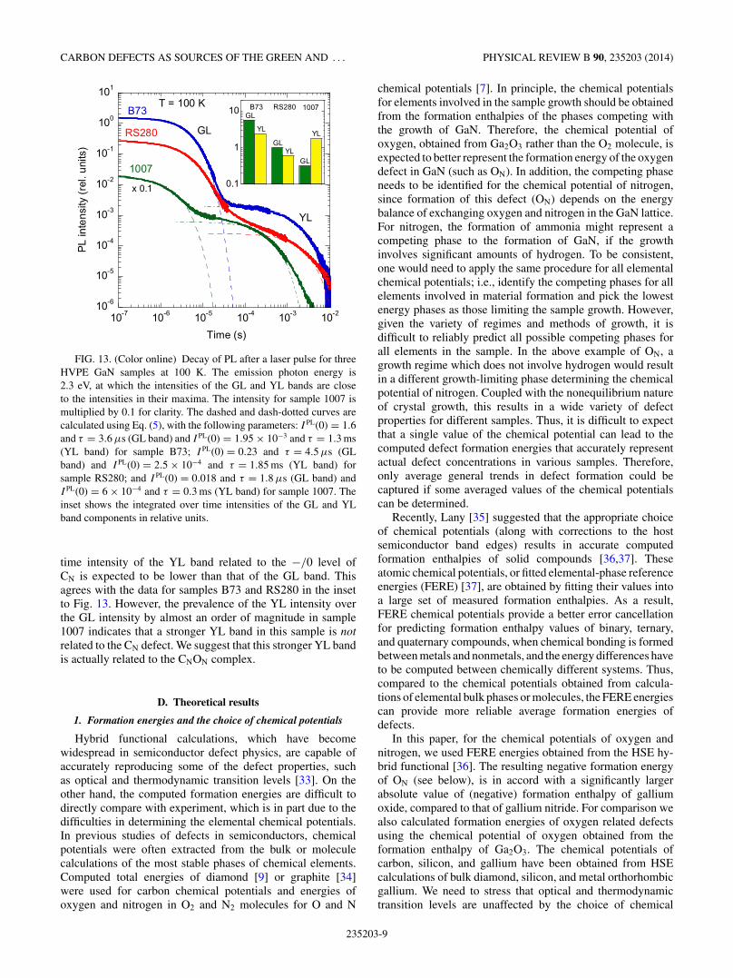
FIG. 13. (Color online) Decay of PL after a laser pulse for threeHVPE GaN samples at 100 K. The emission photon energy is2.3 eV, at which the intensities of the GL and YL bands are closeto the intensities in their maxima. The intensity for sample 1007 ismultiplied by 0.1 for clarity. The dashed and dash-dotted curves arecalculated using Eq. (5), with the following parameters: I PL(0) = 1.6and τ = 3.6 μs (GL band) and I PL(0) = 1.95 × 10⁻³ and τ = 1.3 ms(YL band) for sample B73; I PL(0) = 0.23 and τ = 4.5 μs (GLband) and I PL(0) = 2.5 × 10⁻⁴ and τ = 1.85 ms (YL band) forsample RS280; and I PL(0) = 0.018 and τ = 1.8 μs (GL band) andI PL(0) = 6 × 10⁻⁴ and τ = 0.3 ms (YL band) for sample 1007. Theinset shows the integrated over time intensities of the GL and YLband components in relative units.
time intensity of the YL band related to the −/0 level ofCN is expected to be lower than that of the GL band. Thisagrees with the data for samples B73 and RS280 in the insetto Fig. 13. However, the prevalence of the YL intensity overthe GL intensity by almost an order of magnitude in sample1007 indicates that a stronger YL band in this sample is notrelated to the CN defect. We suggest that this stronger YL bandis actually related to the CNON complex.
D. Theoretical results
1. Formation energies and the choice of chemical potentials
Hybrid functional calculations, which have becomewidespread in semiconductor defect physics, are capable ofaccurately reproducing some of the defect properties, suchas optical and thermodynamic transition levels [33]. On theother hand, the computed formation energies are difficult todirectly compare with experiment, which is in part due to thedifficulties in determining the elemental chemical potentials.In previous studies of defects in semiconductors, chemicalpotentials were often extracted from the bulk or moleculecalculations of the most stable phases of chemical elements.Computed total energies of diamond [9] or graphite [34]were used for carbon chemical potentials and energies ofoxygen and nitrogen in O2 and N2 molecules for O and N
chemical potentials [7]. In principle, the chemical potentialsfor elements involved in the sample growth should be obtainedfrom the formation enthalpies of the phases competing withthe growth of GaN. Therefore, the chemical potential ofoxygen, obtained from Ga2O3 rather than the O2 molecule, isexpected to better represent the formation energy of the oxygendefect in GaN (such as ON). In addition, the competing phaseneeds to be identified for the chemical potential of nitrogen,since formation of this defect (ON) depends on the energybalance of exchanging oxygen and nitrogen in the GaN lattice.For nitrogen, the formation of ammonia might represent acompeting phase to the formation of GaN, if the growthinvolves significant amounts of hydrogen. To be consistent,one would need to apply the same procedure for all elementalchemical potentials; i.e., identify the competing phases for allelements involved in material formation and pick the lowestenergy phases as those limiting the sample growth. However,given the variety of regimes and methods of growth, it isdifficult to reliably predict all possible competing phases forall elements in the sample. In the above example of ON, agrowth regime which does not involve hydrogen would resultin a different growth-limiting phase determining the chemicalpotential of nitrogen. Coupled with the nonequilibrium natureof crystal growth, this results in a wide variety of defectproperties for different samples. Thus, it is difficult to expectthat a single value of the chemical potential can lead to thecomputed defect formation energies that accurately representactual defect concentrations in various samples. Therefore,only average general trends in defect formation could becaptured if some averaged values of the chemical potentialscan be determined.
Recently, Lany [35] suggested that the appropriate choiceof chemical potentials (along with corrections to the hostsemiconductor band edges) results in accurate computedformation enthalpies of solid compounds [36,37]. Theseatomic chemical potentials, or fitted elemental-phase referenceenergies (FERE) [37], are obtained by fitting their values intoa large set of measured formation enthalpies. As a result,FERE chemical potentials provide a better error cancellationfor predicting formation enthalpy values of binary, ternary,and quaternary compounds, when chemical bonding is formedbetween metals and nonmetals, and the energy differences haveto be computed between chemically different systems. Thus,compared to the chemical potentials obtained from calcula-tions of elemental bulk phases or molecules, the FERE energiescan provide more reliable average formation energies ofdefects.
In this paper, for the chemical potentials of oxygen andnitrogen, we used FERE energies obtained from the HSE hy-brid functional [36]. The resulting negative formation energyof ON (see below), is in accord with a significantly largerabsolute value of (negative) formation enthalpy of galliumoxide, compared to that of gallium nitride. For comparison wealso calculated formation energies of oxygen related defectsusing the chemical potential of oxygen obtained from theformation enthalpy of Ga2O3. The chemical potentials ofcarbon, silicon, and gallium have been obtained from HSEcalculations of bulk diamond, silicon, and metal orthorhombicgallium. We need to stress that optical and thermodynamictransition levels are unaffected by the choice of chemical
235203-9
RESHCHIKOV, DEMCHENKO, USIKOV, HELAVA, AND MAKAROV PHYSICAL REVIEW B 90, 235203 (2014)
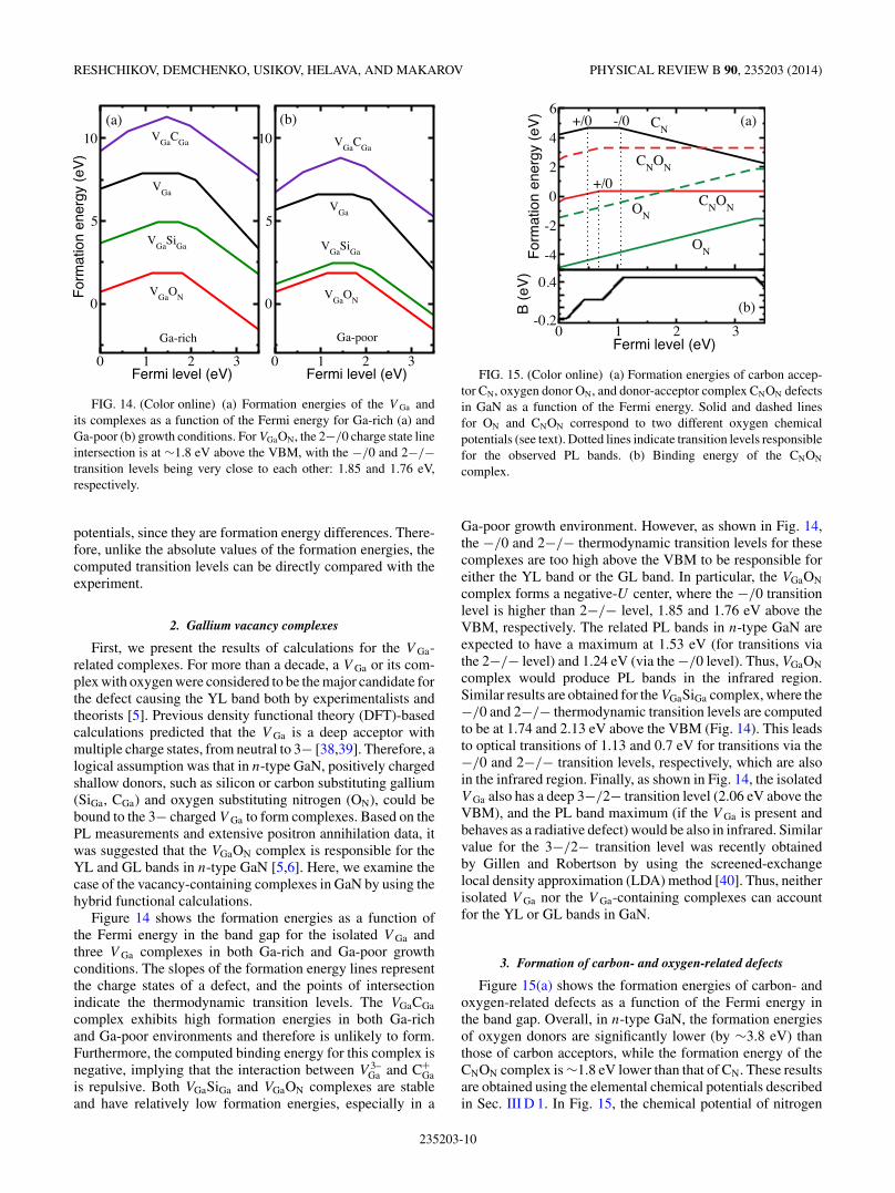
FIG. 14. (Color online) (a) Formation energies of the V Ga andits complexes as a function of the Fermi energy for Ga-rich (a) andGa-poor (b) growth conditions. For VGaON, the 2−/0 charge state lineintersection is at ∼1.8 eV above the VBM, with the −/0 and 2−/−transition levels being very close to each other: 1.85 and 1.76 eV,respectively.
potentials, since they are formation energy differences. There-fore, unlike the absolute values of the formation energies, thecomputed transition levels can be directly compared with theexperiment.
2. Gallium vacancy complexes
First, we present the results of calculations for the V Ga-related complexes. For more than a decade, a V Ga or its com-plex with oxygen were considered to be the major candidate forthe defect causing the YL band both by experimentalists andtheorists [5]. Previous density functional theory (DFT)-basedcalculations predicted that the V Ga is a deep acceptor withmultiple charge states, from neutral to 3− [38,39]. Therefore, alogical assumption was that in n-type GaN, positively chargedshallow donors, such as silicon or carbon substituting gallium(SiGa, CGa) and oxygen substituting nitrogen (ON), could bebound to the 3− charged V Ga to form complexes. Based on thePL measurements and extensive positron annihilation data, itwas suggested that the VGaON complex is responsible for theYL and GL bands in n-type GaN [5,6]. Here, we examine thecase of the vacancy-containing complexes in GaN by using thehybrid functional calculations.
Figure 14 shows the formation energies as a function ofthe Fermi energy in the band gap for the isolated V Ga andthree V Ga complexes in both Ga-rich and Ga-poor growthconditions. The slopes of the formation energy lines representthe charge states of a defect, and the points of intersectionindicate the thermodynamic transition levels. The VGaCGa
complex exhibits high formation energies in both Ga-richand Ga-poor environments and therefore is unlikely to form.Furthermore, the computed binding energy for this complex isnegative, implying that the interaction between V 3–
Ga and C+Ga
is repulsive. Both VGaSiGa and VGaON complexes are stableand have relatively low formation energies, especially in a
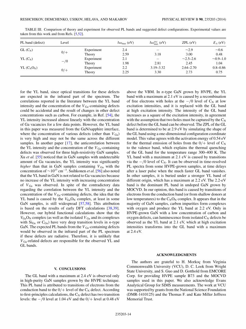
FIG. 15. (Color online) (a) Formation energies of carbon accep-tor CN, oxygen donor ON, and donor-acceptor complex CNON defectsin GaN as a function of the Fermi energy. Solid and dashed linesfor ON and CNON correspond to two different oxygen chemicalpotentials (see text). Dotted lines indicate transition levels responsiblefor the observed PL bands. (b) Binding energy of the CNON
complex.
Ga-poor growth environment. However, as shown in Fig. 14,the −/0 and 2−/− thermodynamic transition levels for thesecomplexes are too high above the VBM to be responsible foreither the YL band or the GL band. In particular, the VGaON
complex forms a negative-U center, where the −/0 transitionlevel is higher than 2−/− level, 1.85 and 1.76 eV above theVBM, respectively. The related PL bands in n-type GaN areexpected to have a maximum at 1.53 eV (for transitions viathe 2−/− level) and 1.24 eV (via the −/0 level). Thus, VGaON
complex would produce PL bands in the infrared region.Similar results are obtained for the VGaSiGa complex, where the−/0 and 2−/− thermodynamic transition levels are computedto be at 1.74 and 2.13 eV above the VBM (Fig. 14). This leadsto optical transitions of 1.13 and 0.7 eV for transitions via the−/0 and 2−/− transition levels, respectively, which are alsoin the infrared region. Finally, as shown in Fig. 14, the isolatedV Ga also has a deep 3−/2− transition level (2.06 eV above theVBM), and the PL band maximum (if the V Ga is present andbehaves as a radiative defect) would be also in infrared. Similarvalue for the 3−/2− transition level was recently obtainedby Gillen and Robertson by using the screened-exchangelocal density approximation (LDA) method [40]. Thus, neitherisolated V Ga nor the V Ga-containing complexes can accountfor the YL or GL bands in GaN.
3. Formation of carbon- and oxygen-related defects
Figure 15(a) shows the formation energies of carbon- andoxygen-related defects as a function of the Fermi energy inthe band gap. Overall, in n-type GaN, the formation energiesof oxygen donors are significantly lower (by ∼3.8 eV) thanthose of carbon acceptors, while the formation energy of theCNON complex is ∼1.8 eV lower than that of CN. These resultsare obtained using the elemental chemical potentials describedin Sec. III D 1. In Fig. 15, the chemical potential of nitrogen
235203-10

CARBON DEFECTS AS SOURCES OF THE GREEN AND . . . PHYSICAL REVIEW B 90, 235203 (2014)
is not adjusted by the formation enthalpy of GaN, and theresults represent the nitrogen-rich conditions, as commonlyreferred to in the literature. While oxygen is the most abundantdonor in GaN in most cases, the concentration of carbon canexceed that of oxygen in some MOCVD samples (Table I).However, even with the same growth method (MOCVD), bothconductive samples (with more oxygen donors) and insulatingsamples (with more carbon) can be obtained. This suggeststhat the absolute values of formation energy computed with anytheoretical method, which assumes equilibrium conditions, areat best rough guidelines for expected relative concentrationsof impurities. The SIMS measurements suggest that thenonequilibrium incorporation of carbon into GaN (in eitherthe CN acceptor or CNON configuration) in some cases couldbe similar to that of the oxygen donor ON. For comparison,dashed lines in Fig. 15(a) show the results for ON andCNON computed using the oxygen chemical potential obtainedfrom Ga2O3. In this case, the formation energies of CN andON become comparable (which could be the case in someMOCVD samples). Thus, different competing phases duringdifferent regimes of growth can create favorable conditions forthe formation of either isolated carbon acceptor CN, in somecases, or the CNON complex, in other cases.
The thermodynamic transition levels of the CN acceptor,CNON complex, and ON donor have been published elsewhere[7,9]. The CN acceptor is found to have two transition levels[Fig. 15(a)]: the 0/+ transition level at 0.48 eV above theVBM and the −/0 transition level at 1.04 above the VBM.Interestingly, a defect commonly thought of as an acceptorcan also exhibit a donor-like + charge state. This is due toseveral electronic states that the defect creates in the band gap.For example, both CN and CNON create three electronic defectstates in the band gap (shown in Ref. [7]). In the neutral stateof CN, two of these defect states are occupied by electrons(all three states are occupied in CNO0
N). The addition of anelectron leads to the −/0 transition level, and the removal ofan electron leads to the 0/+ level in the band gap. Detailedcalculations show that numerous defects have multiple chargestates in wide band gap semiconductors, especially defectcomplexes that often create multiple defect states in theband gap.
The 0/+ transition level of the ON donor is found to be0.14 eV below the CBM. The transition levels for the CNON
complex are 0.14 eV above the VBM for the +/2+ level and0.75 eV for the 0/+ level. The −/0 transition level of CN isdeeper than the 0/+ level of CNON complex, suggesting thatthe YL band generated by CN should be shifted to energieslower than that from the CNON complex.
Most importantly, the calculations presented in Fig. 15confirm that the difference in the transition level structurefor the two carbon defects (CN and CNON) allows forthe possibility to distinguish between the different sourcesof the YL band. In samples where carbon is mostly bound intothe CNON complex, only a single YL band should be observedsince there is only one possible transition, via the 0/+ level.However, if carbon exists mostly in the form of isolated CN
defects, two PL bands are possible. Along with the YL bandcaused by transitions via the −/0 level of CN, the secondary PLband can be activated by increasing optical excitation intensity.This will happen when a second hole is captured by a neutral
FIG. 16. (Color online) Schematic configuration coordinate di-agrams for the CN acceptor (a) and (b) and for the CNON donor(c). The optical transitions are shown with arrows: downward forPL (emission) and upward for the resonant excitation of a defect(absorption). (a) Absorption and emission via the (−/0 transitionlevel of CN; (b) transitions via the 0/+ level of CN; (c) transitionsvia the 0/+ level of the CNON complex; and (d) band diagram withtransition levels.
CN defect, with subsequent emission via the 0/+ level of theCN defect.
4. Optical transitions
Due to the existence of the three carbon-related transitionlevels, the 0/+ and −/0 levels for CN and the 0/+ levelfor CNON, three well-separated PL bands can be observedexperimentally in the visible part of the spectrum. Figure 16illustrates the optical transitions via the CN and CNON
defects.While optical transitions via the isolated carbon acceptor
CN have been suggested to produce the YL band [8], wefind that the transitions via this acceptor should producea PL band with a maximum at 1.98 eV and a ZPL at2.45 eV. In n-type GaN, this acceptor is negatively chargedin the ground state (Fig. 15). Once the electron-hole pairis created with above-band-gap laser illumination, the holeis captured by the negatively charged acceptor in ∼10−10 s,changing its charge state to neutral (if the defect were excitedresonantly with below-band-gap light, the maximum of thecharacteristic excitation band would be at 2.81 eV, accordingto our calculations). Since the PL lifetime is relatively long, asecond hole can be captured by the neutral CN defect due to theexistence of the 0/+ transition level of CN in the band gap. Asa result, radiative recombination can occur, with a free electronrecombining with a hole at C+
N. This transition is shown witha downward arrow in Fig. 16(b). The energy of this transitionis computed to be 2.59 eV and is between green and blue inthe visible range. The ZPL for this transition is computed tobe 3.00 eV. The yellow (or orange) PL band with a maximumat 1.98 eV is generated by the CN defect and should have alower PL band maximum than the PL band generated by theCNON complex [Fig. 16(c)]. The CNON complex is expected
235203-11

RESHCHIKOV, DEMCHENKO, USIKOV, HELAVA, AND MAKAROV PHYSICAL REVIEW B 90, 235203 (2014)
to produce a PL band with a maximum at 2.25 eV and a ZPLat 2.73 eV.
Overall, the calculated trends are such that in samples wherecarbon is bound into the CNON complex, only one PL band(yellow) is possible, while in samples where the carbon ispredominantly isolated as the CN acceptor, two PL bands arepossible: yellow (or orange) and green (or green-blue). Thesetrends are in quantitative agreement with experimental data,as will be discussed in Sec. IV.
Finally, it may appear surprising that both donors andacceptors can cause the YL band in GaN. It is commonlythought that an acceptor is a much more natural candidatefor this process, since a negatively charged acceptor shouldcapture holes more efficiently. However, a neutral deep donoris also capable of capturing a hole, albeit with a capture crosssection lower by about an order of magnitude [41]. In addition,some published results of electron paramagnetic resonancemeasurements indicate that the YL band is associated witha deep donor rather than an acceptor [42]. The g factorsdetermined for the YL band with a maximum at 2.2 eV(g|| = 1.989 and g⊥ = 1.992) are smaller than the free electronvalue of g, which indicates that the related defect may indeedbe a deep donor [42].
5. Stability of the CNON complex
The binding energy B of the CNON complex for a range ofFermi energies is shown in Fig. 15(b). While this complex isunstable in p-type GaN, the binding energy of this complex inn-type GaN is 0.46 eV. Since the complex is formed by the nextnearest neighbor atoms in the GaN lattice, this binding energyis relatively low. However, the binding energy provides limitedinformation about the stability of the complex. In order toestimate the stability of the complex, we calculated the CNON
complex dissociation barriers using HSE and generalizedgradient approximation (GGA).
The CNON complex can dissociate by the jump of either aC or O atom into an interstitial site, leaving behind a nitrogenvacancy (V N). However, our HSE calculations for n-type GaNshow that the formation energies are high for stable interstitialOi and split-interstitial Ci: 3 to 5.5 eV higher than those of theON and CN defects, which agrees with previously publishedresults [9,43,44]. Additionally, our calculations show that inthe presence of the V N formed in place of the CN or ON defects,both the split-interstitial carbon and interstitial oxygen areunstable. Therefore, the dissociation of the CNON complex viadiffusion of either oxygen or carbon into the nearest interstitialsites is energetically unfavorable.
Even if a V N was already present as a nearest neighbor ofthe CNON complex (which is unlikely, due to the negligibleconcentrations of V N in n-type GaN and the absence ofattractive interaction between V N and CNON), migration ofoxygen into the V N would not be favorable. The nudgedelastic band calculations based on GGA reveal a diffusionbarrier for this process of 1.7 eV. Assuming the typical phononfrequency of 1013 s−1 and following Ref. [45], we estimate thatin this case, the complex remains stable for temperatures up to∼660 K. Thus, when the CNON complexes are formed duringgrowth, they are likely stable.
IV. DISCUSSION
A. Yellow and blue luminescence bands in undopedand C-doped GaN
In MOCVD-grown n-type GaN, only the YL band isobserved in the defect-related part of the PL spectrum (Fig. 2).With increasing excitation intensity, the YL band intensitysaturates, and no other bands appear at higher photon energies.If the YL band in this sample was caused by electron transitionsvia the −/0 state of the isolated CN defect, then it is expectedthat a PL band related to transitions via the 0/+ level shouldemerge at higher photon energies, which is not observed inFig. 2. Thus, the absence of any PL band in the range from2.6 to 3 eV in n-type GaN (Fig. 2) is an indication that theYL band in the MOCVD-grown GaN (sample EM1256) isnot related to the isolated CN defect. In contrast, the CNON
complex can explain the YL in this sample, since it does nothave the transition levels necessary to produce an additionalPL band in this range.
In the literature, there is controversial information regardingthe blue band in GaN, which, according to Ref. [9], couldbe assigned to the 0/+ transition level of the CN acceptor.A careful analysis suggests that this is unlikely. Indeed, ablue band is often observed in C-doped GaN, along withthe YL band [10–13,46]. However, closer inspection of theluminescence spectra in these papers allows us to conclude thatat least two different defect-related blue bands were observed.A band with a maximum at 2.85–2.86 eV (the BL band) wasobserved in GaN grown by molecular beam epitaxy (MBE)[12,13], and a broader band with a maximum at 3.0 eV (theBL2 band) was observed in GaN grown by MOCVD [10,11].In Ref. [12], where the excitation intensity was extremely high(400 kW/cm2), the intensity of the YL band was about anorder of magnitude higher than that of the BL band in all ofthe high-resistivity GaN samples doped with carbon. This isinconsistent with a model according to which the YL and BLbands are caused by two charge states of the same defect [9].Indeed, the intensity of the YL band should be much lower thanthat the BL band since the defect is almost completely saturatedwith holes in such experimental conditions. At lower excitationintensities (20 W/cm2), the intensity of the BL band (relativeto the YL band) decreased with increasing concentration of Cfrom 2 × 10¹⁸ to 2 × 1019 cm−3 [13]. We assume that the BLband observed in Refs. [12,13] is caused by the ZnGa acceptor,since the BL band with a maximum at 2.9 eV is strong evenat low levels of contamination with Zn (lower than 1016 cm−3)[5]. It is also unlikely that the BL band in C-doped GaN isrelated to Mg, because the Mg-related BL band appears onlyin GaN heavily doped with Mg, and it greatly shifts withincreasing excitation intensity [47]. No shifts were observedfor the BL band in the MBE-grown GaN. [13].
In MOCVD-grown GaN, a broad band with a maximum at3.0 eV is identified as the BL2 band [24,25]. The BL2 bandis quenched above 75 K with an activation energy of about150 meV [25], which is very similar to the results reported inRef. [11]. It is interesting to note that a very similar quenchingof the BL2 band with increasing temperature from 15 to150 K and the dominance of the Zn-related BL band at highertemperatures was observed in Refs. [13,25]. The BL2 banddemonstrates a characteristic metastable behavior; namely,
235203-12

CARBON DEFECTS AS SOURCES OF THE GREEN AND . . . PHYSICAL REVIEW B 90, 235203 (2014)
it bleaches considerably under continuous above-band-gapillumination, as the YL band simultaneously rises [25]. Thebleaching has been attributed to a recombination-assisted dis-sociation of a defect complex, apparently containing hydrogenas a component [5]. A very similar behavior of the 3.0 eV bandin C-doped GaN was reported in Ref. [11]. Note that a strongblue band with a maximum at 3.05 eV was observed in C-doped([C] = 1.5 × 1018 cm−3), conductive (n = 1018 cm−3) GaNgrown by MOCVD [46]. The blue band in Ref. [46] becamemuch stronger than the YL band after treatment in hydrogenplasma at 200 °C for 1 h. This may indicate that the authors ofRef. [46] observed the BL2 band related to a defect complexcontaining hydrogen. In some GaN samples (undoped, Cdoped, and Fe doped), the fine structure of the BL2 band isobserved, with the ZPL at 3.34 eV [25]. From the position ofthe ZPL, it was suggested that the transition level responsiblefor the BL2 band is located at 0.15 eV above the valence band[24]. Summarizing the above information, we suggest that bluebands sometimes observed in C-doped GaN have no relationto the isolated CN defect.
B. Yellow and green luminescence bandsin GaN grown by HVPE
The GL band with a maximum at 2.4 eV is observed onlyin high-quality GaN grown by the HVPE technique. In free-standing GaN (sample B73), the defect responsible for the GLband is the dominant deep-level defect, with a concentrationof about 1015 cm−3 (Ref. [6]). From temperature-dependentHall effect measurements, the total concentration of acceptorsin a similar sample has been estimated to be 2.4 × 1015 cm−3
(Ref. [48]). From the SIMS analysis of similar freestandingGaN, it was found that the concentrations of oxygen andcarbon are on the order of 1016 cm−3 each, where the ON defect(with a concentration of 7.8 × 1015 cm−3 from Hall effectmeasurements) is the main shallow donor in these samples[49,50]. Since the GL band intensity increases as a square ofthe excitation intensity [6], it is reasonable to attribute thisband to transitions of electrons from the conduction band tothe 0/+ level of the CN defect. In this case, the YL bandcan be caused by transitions via the −/0 level of the samedefect.
Analysis of the time-resolved PL spectra in GaN samplesexhibiting a strong GL band (Fig. 9 for sample RS280 andFig. 4 in Ref. [51] for freestanding GaN) indicates that the YLband, related to the −/0 level of CN, has a maximum at 2.1 eV.In these high-purity HVPE samples, the integrated over timeintensity of the YL band after pulsed excitation is only slightlylower than that of the GL band (inset in Fig. 13), which is inagreement with the assumption that the YL band and the GLband are associated with transitions via different charge levelsof the same defect.
However, in less pure HVPE samples (such as sample1007) and apparently all MOCVD samples, another defectis responsible for the dominant YL band, which has amaximum at 2.2 eV. Previously, we attributed this YL bandto the CNON complex [7]. The saturation of this YL bandin MOCVD samples is not followed by the emergenceof any other PL band at higher photon energies (Fig. 2).This suggests that in MOCVD samples the YL band is
produced by the CNON complex, and isolated carbon CN is notfound.
On the other hand, in HVPE-grown GaN layers on sapphire(more than 20 samples studied in this paper), the intensitiesof the YL bands originating from the CN and CNON defectsmay be comparable. For the samples of highest purity, such assample RS280, the CN-related band is the dominant YL band.In these samples, the integrated over time intensities of theYL and GL bands after a laser pulse are nearly equal to eachother, which is consistent with the assignment of these bandsto two different charge states of the same defect. In less puresamples, such as sample 1007, the CNON-related YL band isdominant. In this case, the integrated over time intensity of theYL band is about 10 times higher than that for the GL band.Thus, we expect that in this sample, the concentration of theCNON defects is higher than that of the CN defects by roughlyan order of magnitude. It appears that only in GaN sampleswith very low concentrations of carbon and oxygen impurities,the isolated CN defects may be the dominant defects causingthe YL and GL bands, whereas in samples with relatively highconcentration of either C, O, or both, the CNON complexes arelikely to be formed and will cause the YL band but not the GLband.
C. Comparison of theory and experiment
The experimental and theoretical findings are summarizedin Table III. The characteristic excitation band maximum,�ωexc
max, for the YL band (assumed to be related to the CNON
complex) in GaN was estimated to be 3.19 eV (Ref. [52])and 3.32 eV (Ref. [53]) from the analysis of the shape ofthe PL excitation (PLE) spectrum. Note that a significantpart of the characteristic excitation band was obscured inthese experiments due to the contribution of band-to-bandexcitation in the PLE spectrum. We expect that this may resultin an uncertainty of about ±0.1 eV in the determination of�ωexc
max. The experimental value of the ZPL for the YL band(2.64–2.70 eV) was found as the middle point between thethreshold of the PL band and that of the PLE band [5,52].The experimental values of ZPL for the CN-related GL andYL bands in the studied HVPE-grown GaN samples wereestimated from the best fits of the PL band shape with Eq. (1).To account for possible errors in these estimates, we roundedthe values and added tilde marks in Table III. The distanceof the defect level from the VBM, EA, was calculated as thedifference between the band-gap energy and the ZPL.
Overall, the experimental values agree very well with thecalculated ones. In most cases, the disagreement betweencalculations and experiment does not exceed 0.1 eV. The closeagreement allows us to draw the conclusion that there are twoseparate sources of the YL band in different samples, namely,the isolated CN defect and the CNON complex. These twocases can be distinguished by the presence of the GL bandonly in some high-quality samples containing mostly isolatedCN acceptors.
D. V Ga-related defects as a source of the YL band
According to our hybrid functional calculations, neitherV Ga nor its complexes with ON, SiGa, or CGa can be responsible
235203-13
RESHCHIKOV, DEMCHENKO, USIKOV, HELAVA, AND MAKAROV PHYSICAL REVIEW B 90, 235203 (2014)
TABLE III. Comparison of theory and experiment for observed PL bands and suggested defect configurations. Experimental values aretaken from this work and from Refs. [5,52].
PL band (defect) Level �ωmax (eV) �ωexcmax (eV) ZPL (eV) EA (eV)
GL (CN)0/+ Experiment 2.4 − ∼2.9 ∼0.6
Theory 2.59 3.18 3.00 0.48YL (CN) −/0
Experiment 2.1 − ∼2.5–2.6 ∼0.9–1.0Theory 1.98 2.81 2.45 1.04
YL (CNON)0/+ Experiment 2.2 3.19–3.32 2.64–2.70 0.8–0.86
Theory 2.25 3.30 2.73 0.75
for the YL band, since optical transitions for these defectsare expected in the infrared part of the spectrum. Thecorrelations reported in the literature between the YL bandintensity and the concentration of the V Ga-containing defectscould be accidental and the result of changes in other defectconcentrations such as carbon. For example, in Ref. [54], theYL intensity increased almost linearly with the concentrationof Ga vacancies for a few data points. However, the YL bandin this paper was measured from the GaN/sapphire interface,where the concentration of various defects (other than V Ga)is very high and may not be the same across the differentsamples. In another paper [17], the anticorrelation betweenthe YL intensity and the concentration of the V Ga-containingdefects was observed for three high-resistivity GaN samples.Xu et al. [55] noticed that in GaN samples with undetectableamount of Ga vacancies, the YL intensity was significantlyhigher than that in GaN samples containing V Ga with theconcentration of ∼1017 cm−3. Suihkonen et al. [56] also notedthat the YL band in GaN is not related to Ga vacancies becauseno increase of the YL intensity with increasing concentrationof V Ga was observed. In spite of the contradictory dataregarding the correlation between the YL intensity and theconcentration of the V Ga-containing defects, the idea that theYL band is caused by the VGaON complex, at least in someGaN samples, is still widespread [57,58]. This attributionis based on the results of early DFT calculations [38,39].However, our hybrid functional calculations show that theVGaON complex (as well as the isolated V Ga and its complexeswith SiGa or CGa) have very deep transition levels in n-typeGaN. The expected PL bands from the V Ga-containing defectswould be observed in the infrared part of the PL spectrumif these defects are radiative. Therefore, it is unlikely thatV Ga-related defects are responsible for the observed YL andGL bands.
V. CONCLUSIONS
The GL band with a maximum at 2.4 eV is observed onlyin high-purity GaN samples grown by the HVPE technique.This PL band is attributed to transitions of electrons from theconduction band to the 0/+ level of the CN defect. Accordingto first-principles calculations, the CN defect has two transitionlevels: the −/0 level at 1.04 eV and the 0/+ level at 0.48 eV
above the VBM. In n-type GaN grown by HVPE, the YLband with a maximum at 2.1 eV is caused by a recombinationof free electrons with holes at the −/0 level of CN at lowexcitation intensities, and it is replaced with the GL bandat high excitation intensity. The intensity of the GL bandincreases as a square of the excitation intensity, in agreementwith the assumption that two holes must be captured by the CN
defect before the GL band can be observed. The ZPL of the GLband is determined to be at 2.9 eV by simulating the shape ofthe GL band using a one-dimensional configuration coordinatemodel. This value agrees with the activation energy of 0.54 eVfor the thermal emission of holes from the 0/+ level of CN
to the valence band, which explains the thermal quenchingof the GL band for the temperature range 300–400 K. TheYL band with a maximum at 2.1 eV is caused by transitionsvia the −/0 level of CN. It can be observed in time-resolvedPL spectra from some HVPE-grown samples, at time delaysafter a laser pulse when the much faster GL band vanishes.In other samples, it is buried under a stronger YL band ofdifferent origin, which has a maximum at 2.2 eV. The 2.2-eVband is the dominant PL band in undoped GaN grown byMOCVD. In our opinion, this band is caused by transitions ofelectrons from the conduction band (or from shallow donors atlow temperatures) to the CNON complex. It appears that in themajority of GaN samples, carbon impurities form complexeswith oxygen and produce the YL band at 2.2 eV. Only inHVPE-grown GaN with a low concentration of carbon andoxygen defects, can luminescence from isolated CN defects beobserved as the YL band at 2.1 eV, which at high excitationintensities transforms into the GL band with a maximumat 2.4 eV.
ACKNOWLEDGMENTS
The authors are grateful to H. Morkoc from VirginiaCommonwealth University (VCU), D. C. Look from WrightState University, and S. Guo and D. Gotthold from EMCORECorp. for providing HVPE sample B73 and the MOCVDsamples used in this paper. We also acknowledge EvansAnalytical Group for SIMS measurements. The work at VCUwas supported by grants from the National Science Foundation(DMR-1410125) and the Thomas F. and Kate Miller JeffressMemorial Trust.
235203-14
CARBON DEFECTS AS SOURCES OF THE GREEN AND . . . PHYSICAL REVIEW B 90, 235203 (2014)
[1] Y. Saitoh, K. Sumiyoshi, M. Okada, T. Horii, T. Miyazaki,H. Shiomi, M. Ueno, K. Katayama, M. Kiyama, and T.Nakamura, Appl. Phys. Express 3, 081001 (2010).
[2] Y. Wang, H. Xu, S. Alur, Y. Sharma, F. Tong, P. Gartland,T. Issacs-Smith, C. Ahyi, J. Williams, M. Park, G. Wheeler, M.Johnson, A. A. Allerman, A. Hanser, T. Paskova, E. A. Preble,and K. R. Evans, Phys. Status Solidi C 8, 2430 (2011).
[3] J. Everts, J. van den Keybus, M. Van Hove, D. Visalli,P. Srivastava, D. Marcon, Kai Cheng, M. Leys, S. Decoutere, J.Driesen, and G. Borghs, IEEE Electron Device Lett. 32, 1370(2011).
[4] M.-W. Ha, C. H. Roh, D. W. Hwang, H. G. Choi, H. J. Song,J. H. Lee, J. H. Park, O. Seok, J. Lim, M.-K. Han, and C.-K.Hahn, Jpn. J. Appl. Phys. 50, 06GF17 (2011).
[5] M. A. Reshchikov and H. Morkoc, J. Appl. Phys. 97, 061301(2005).
[6] M. A. Reshchikov, H. Morkoc, S. S. Park, and K. Y. Lee, Appl.Phys. Lett. 81, 4970 (2002).
[7] D. O. Demchenko, I. C. Diallo, and M. A. Reshchikov, Phys.Rev. Lett. 110, 087404 (2013).
[8] J. L. Lyons, A. Janotti, and C. G. Van de Walle, Appl. Phys.Lett. 97, 152108 (2010).
[9] J. L. Lyons, A. Janotti, and C. G. Van de Walle, Phys. Rev. B89, 035204 (2014)
[10] C. H. Seager, A. F. Wright, J. Yu, and W. Gotz, J. Appl. Phys.92, 6553 (2002).
[11] C. H. Seager, D. R. Tallant, J. Yu, and W. Gotz, J. Lumin. 106,115 (2004).
[12] D. S. Green, U. K. Mishra, and J. S. Speck, J. Appl. Phys. 95,8456 (2004).
[13] R. Armitage, Q. Yang, and E. R. Weber, J. Appl. Phys. 97,073524 (2005).
[14] M. A. Reshchikov, J. Appl. Phys. 115, 103503 (2014).[15] D. C. Look, C. E. Stutz, R. J. Molnar, K. Saarinen, and
Z. Liliental-Weber, Solid State Commun. 117, 571 (2001).[16] M. A. Reshchikov, R. H. Patillo, and K. C. Travis, in Proceedings
of the Materials Research Society Symposium, edited by M.Kuball, T. Mukai, T. H. Myers, and J. M. Redwing (MaterialsResearch Society, Warrendale, PA, 2006), Vol. 892, p. FF23.12
[17] F. Reurings and F. Tuomisto, Proc. SPIE 6473, 64730M (2007).[18] M. A. Reshchikov, A. Kvasov, T. McMullen, M. F. Bishop, A.
Usikov, V. Soukhoveev, and V. A. Dmitriev, Phys. Rev. B 84,075212 (2011).
[19] M. A. Reshchikov, M. A. Foussekis, J. D. McNamara, A.Behrends, A. Bakin, and A. Waag, J. Appl. Phys. 111, 073106(2012).
[20] J. Heyd, G. E. Scuseria, and M Ernzerhof, J. Chem. Phys. 118,8207 (2003).
[21] H. Morkoc, Handbook of Nitride Semiconductors and Devices(Wiley, New York, 2008), Vols. 1–3.
[22] S. Lany and A. Zunger, Phys. Rev. B 78, 235104 (2008).[23] M. A. Reshchikov, D. O. Demchenko, J. D. McNamara, S.
Fernandez-Garrido, and R. Calarco, Phys. Rev. B 90, 035207(2014).
[24] M. A. Reshchikov and H. Morkoc, Physica B 376-377, 428(2006).
[25] M. A. Reshchikov, Y. T. Moon, X. Gu, B. Nemeth, J. Nause,and H. Morkoc, Physica B 376-377, 715 (2006).
[26] M. A. Reshchikov, S. S. Park, K. Y. Lee, and H. Morkoc, PhysicaB 340-342, 448 (2003).
[27] C. C. Klick and J. H. Schulman, Solid State Phys. 5, 97 (1957).[28] M. A. Reshchikov, A. Usikov, H. Helava, and Yu. Makarov,
Appl. Phys. Lett. 104, 032103 (2014).[29] M. A. Reshchikov, Appl. Phys. Lett. 88, 202104 (2006).[30] M. A. Reshchikov, Internal Quantum Efficiency of Photo-
luminescence in Wide-Bandgap Semiconductors, Chapter inPhotoluminescence: Applications, Types and Efficacy, editedby M. A. Case and B. C. Stout (Nova Science Publishers, Inc.,New York, 2012), pp. 53–120.
[31] J. F. Muth, J. H. Lee, I. K. Shmagin, R. M. Kolbas, H. C. Casey,B. P. Keller, U. K. Mishra, and S. P. DenBaars, Appl. Phys. Lett.71, 2572 (1997).
[32] M. A. Reshchikov, M. Zafar Iqbal, S. S. Park, K. Y. Lee, D.Tsvetkov, V. Dmitriev, and H. Morkoc, Physica B 340-342, 444(2003).
[33] D. O. Demchenko and M. A. Reshchikov, Phys. Rev. B 88,115204 (2013).
[34] A. F. Wright, J. Appl. Phys. 92, 2575 (2002).[35] S. Lany, Phys. Rev. B 78, 245207 (2008).[36] H. Peng, D. O. Scanlon, V. Stevanovic, J. Vidal, G. W. Watson,
and S. Lany, Phys. Rev. B 88, 115201 (2013).[37] V. Stevanovic, S. Lany, X. Zhang, and A. Zunger, Phys. Rev. B
85, 115104 (2012).[38] J. Neugebauer and C. Van de Walle, Appl. Phys. Lett. 69, 503
(1996).[39] T. Mattila and R. M. Nieminen, Phys. Rev. B 55, 9571
(1997).[40] R. Gillen and J. Robertson, J. Phys.: Condens. Matter 25, 405501
(2013).[41] M. A. Reshchikov and R. Y. Korotkov, Phys. Rev. B 64, 115205
(2001).[42] D. M. Hofmann, D. Kovalev, G. Steude, B. K. Meyer,
A. Hoffmann, L. Eckey, R. Heitz, T. Detchprom, H. Amano, andI. Akasaki, Phys. Rev. B 52, 16702 (1995).
[43] A. F. Wright, J Appl. Phys. 98, 103531 (2005).[44] T. Mattila and R. M. Nieminen, Phys. Rev. B 54, 16676 (1996).[45] S. Limpijumnong and C. G. Van de Walle, Phys. Rev. B 69,
035207 (2004).[46] A. Y. Polyakov, M. Shin, J. A. Freitas, M. Skowronski, D. W.
Greve, and R. G. Wilson, J. Appl. Phys. 80, 6349 (1996).[47] M. A. Reshchikov, G.-C. Yi, and B. W. Wessels, Phys. Rev. B
59, 13176 (1999).[48] D. Huang, F. Yun, P. Visconti, M. A. Reshchikov, D. Wang, H.
Morkoc, D. L. Rode, L. A. Farina, C. Kurdak, K. T. Tsen, S. S.Park, and K. Y. Lee, Solid-State Electron. 45, 711 (2001).
[49] D. C. Look, in Proceedings of the Materials Research SocietySymposium, edited by Y. Arakawa, A. Rizzi, J. S. Speck, C. M.Wetzel, and E. T. Yu (Materials Research Society, Warrendale,PA, 2003), Vol. 743, p. L10.1.
[50] H. Morkoc, Mater. Sci. Eng. R 33, 135 (2001).[51] M. A. Reshchikov, H. Morkoc, S. S. Park, and K. Y. Lee, Appl.
Phys. Lett. 78, 2882 (2001).[52] T. Ogino and M. Aoki, Jpn. J. Appl. Phys. 19, 2395 (1980).[53] M. A. Reshchikov, H. Morkoc, S. S. Park, and K. Y. Lee,
in Proceedings of the Materials Research Society Symposium,edited by S. F. Chichibu, D. C. Look, J. Neugebauer, J. E.Northrup, and H. Riechert (Materials Research Society, War-rendale, PA, 2002), Vol. 693, p. I619.
[54] K. Saarinen, T. Laine, S. Kuisma, J. Nissila, P. Hautojarvi,L. Dobrzynski, J. M. Baranowski, K. Pakula, R. Stepniewski,
235203-15

RESHCHIKOV, DEMCHENKO, USIKOV, HELAVA, AND MAKAROV PHYSICAL REVIEW B 90, 235203 (2014)
M. Wojdak, A. Wysmolek, T. Suski, M. Leszszynski, I. Grze-gory, and S. Porowski, Phys. Rev. Lett. 79, 3030 (1997).
[55] F. J. Xu, B. Shen, L. Lu, Z. L. Miao, J. Song, Z. J. Yang, G. Y.Zhang, X. P. Hao, B. Y. Wang, X. Q. Shen, and H. Okumura,J. Appl. Phys. 107, 023528 (2010).
[56] S. Suihkonen, H. Nykanen, T. Tanikawa, M. Yamaguchi, Y.Honda, and H. Amano, Phys. Status Solidi A 210, 383 (2013).
[57] A. Uedono, T. Fujishima, Y. Cao, Y. Zhang, N.Yoshihara, S. Ishibashi, M. Sumiya, O. Laboutin, W.Johnson, and T. Palacios, Appl. Phys. Lett. 104, 082110(2014).
[58] I.-H. Lee, A. Y. Polyakov, N. B. Smirnov, A. V. Govorkov, A. S.Usikov, H. Helava, Yu. N. Makarov, and S. J. Pearton, J. Appl.Phys. 115, 223702 (2014).
235203-16