cadence nclaunch lab
TRANSCRIPT
HDL
PROGRAMMING
LAB

vhdl
Coding
EXPERIMENT-1
16X1
MULTIPLEXER
16X1 MULTIPLEXER
1. AIM :-
To simulate and synthesize 16*1 multiplexer using Xilinx software.

2. SOFTWARE USED :-
XST(Xilinx Synthesis Tool) for synthesis and
ISE simulator for simulation.
3. INTRODUCTION :-A multiplexer is a digital switch. It connects data from one of n sources to its output. There are n sources of data. There are s inputs that select among n sources so s=log2n. An enable input en allows the multiplexer to do its thing; when en=0 all the outputs are zero. A multiplexer os often called a MUX for short.
Multiplexers are obviously useful devices in any application in which data must be switched from multiple sources to destination. Unlike a mechanical switch, a multiplexer is a unidirectional device that is information flows from inputs to outputs.
Multiplexers are very easy to describe in VHDL. In a dataflow style of architecture, the WITH SELECT statement provides the required functionality. In behavioral style of architecture a CASE STATEMENT is used.
In a 16X1 multiplexer, there are four select inputs which selects one of the sixteen inputs from source as output.
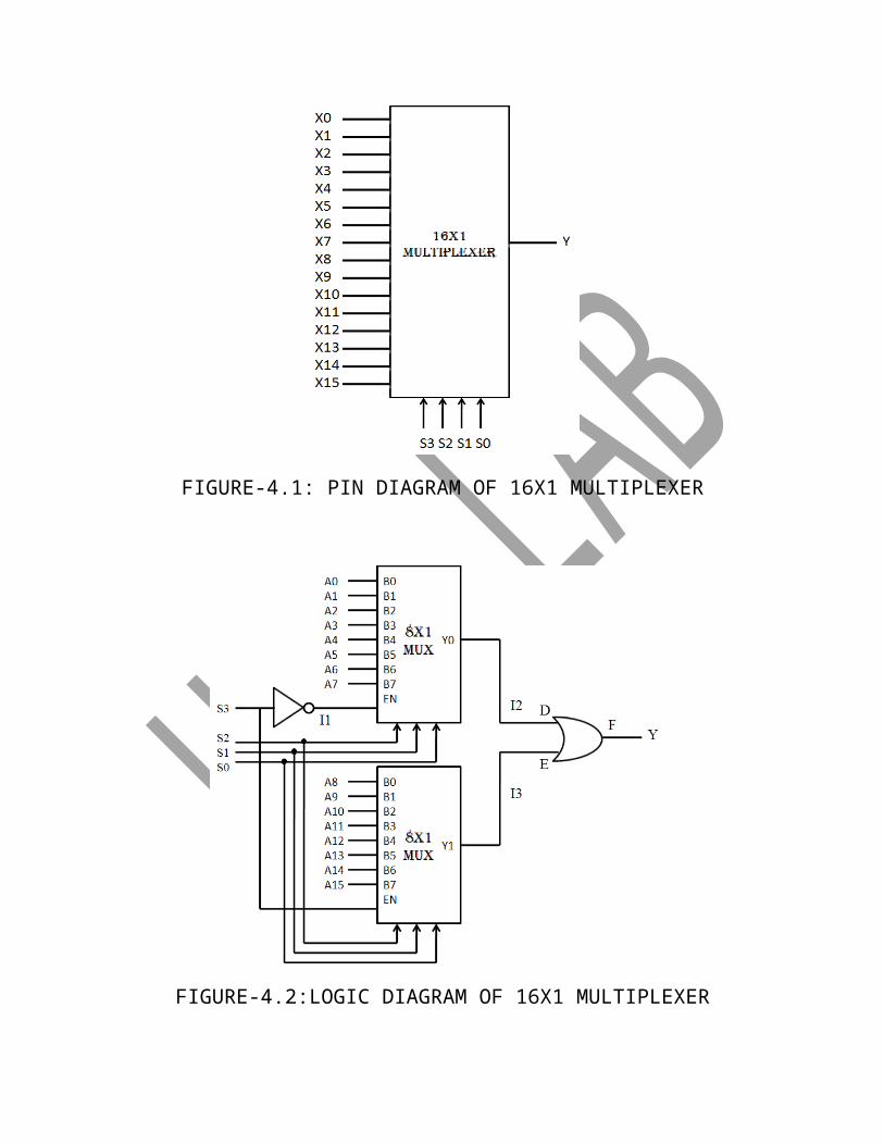
4. PIN DIAGRAM/LOGIC DIAGRAM :-
A. The pin diagram of 16x1 multiplexer is shown in figure 4.1
B. The logic diagram of 16x1 multiplexer is shown in figure 4.2

FIGURE-4.1: PIN DIAGRAM OF 16X1 MULTIPLEXER
FIGURE-4.2:LOGIC DIAGRAM OF 16X1 MULTIPLEXER
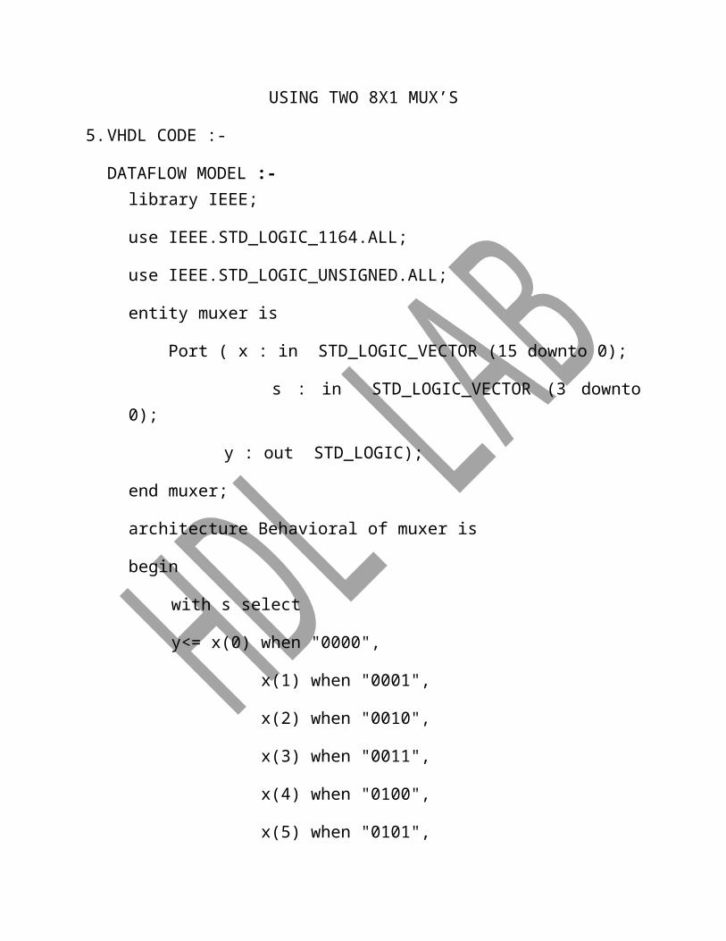
USING TWO 8X1 MUX’S
5. VHDL CODE :-
DATAFLOW MODEL :-library IEEE;
use IEEE.STD_LOGIC_1164.ALL;
use IEEE.STD_LOGIC_UNSIGNED.ALL;
entity muxer is
Port ( x : in STD_LOGIC_VECTOR (15 downto 0);
s : in STD_LOGIC_VECTOR (3 downto 0);
y : out STD_LOGIC);
end muxer;
architecture Behavioral of muxer is
begin
with s select
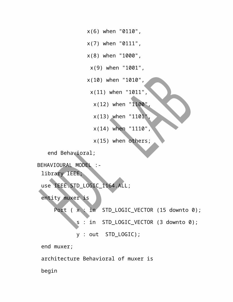
y<= x(0) when "0000",
x(1) when "0001",
x(2) when "0010",
x(3) when "0011",
x(4) when "0100",
x(5) when "0101",
x(6) when "0110",
x(7) when "0111",
x(8) when "1000",
x(9) when "1001",
x(10) when "1010",
x(11) when "1011",
x(12) when "1100",
x(13) when "1101",
x(14) when "1110",
x(15) when others;
end Behavioral;
BEHAVIOURAL MODEL :- library IEEE;
use IEEE.STD_LOGIC_1164.ALL;
entity muxer is
Port ( x : in STD_LOGIC_VECTOR (15 downto 0);
s : in STD_LOGIC_VECTOR (3 downto 0);
y : out STD_LOGIC);
end muxer;
architecture Behavioral of muxer is
begin
process(x,s)
begin
case s is
when "0000" =>y<=x(0);
when "0001" =>y<=x(1);
when "0010" =>y<=x(2);
when "0011" =>y<=x(3);
when "0100" =>y<=x(4);
when "0101" =>y<=x(5);
when "0110" =>y<=x(6);
when "0111" =>y<=x(7);
when "1000" =>y<=x(8);
when "1001" =>y<=x(9);
when "1010" =>y<=x(10);
when "1011" =>y<=x(11);
when "1100" =>y<=x(12);
when "1101" =>y<=x(13);
when "1110" =>y<=x(14);
when others =>y<=x(15);
end case;
end process;
end Behavioral;
STRUCTURAL MODEL :-
library IEEE;
use IEEE.STD_LOGIC_1164.ALL;
entity muxer is
Port ( x : in STD_LOGIC_VECTOR (15 downto 0);
s : in STD_LOGIC_VECTOR (3 downto 0);

y : out STD_LOGIC);
end muxer;
architecture Behavioral of muxer is
component mux1
port(b:in std_logic_vector(7 downto 0);
sg:in std_logic_vector(2 downto 0);
en:in std_logic;
y1:out std_logic);
end component;
component not1
port(l:in std_logic;
m:out std_logic);
end component;
component or1
port(d,e:in std_logic;
f:out std_logic);
end component;
signal i1,i2,i3: std_logic;
begin
m1:mux1 port map(x(7 downto 0),s(2 downto 0),i1,i2);

m2:mux1 port map(x(15 downto 8),s(2 downto 0),s(3),i3);
n1:not1 port map(s(3),i1);
o1:or1 port map(i1,i2,y);
end behavioral;
library IEEE;
use IEEE.STD_LOGIC_1164.ALL;
entity mux1 is
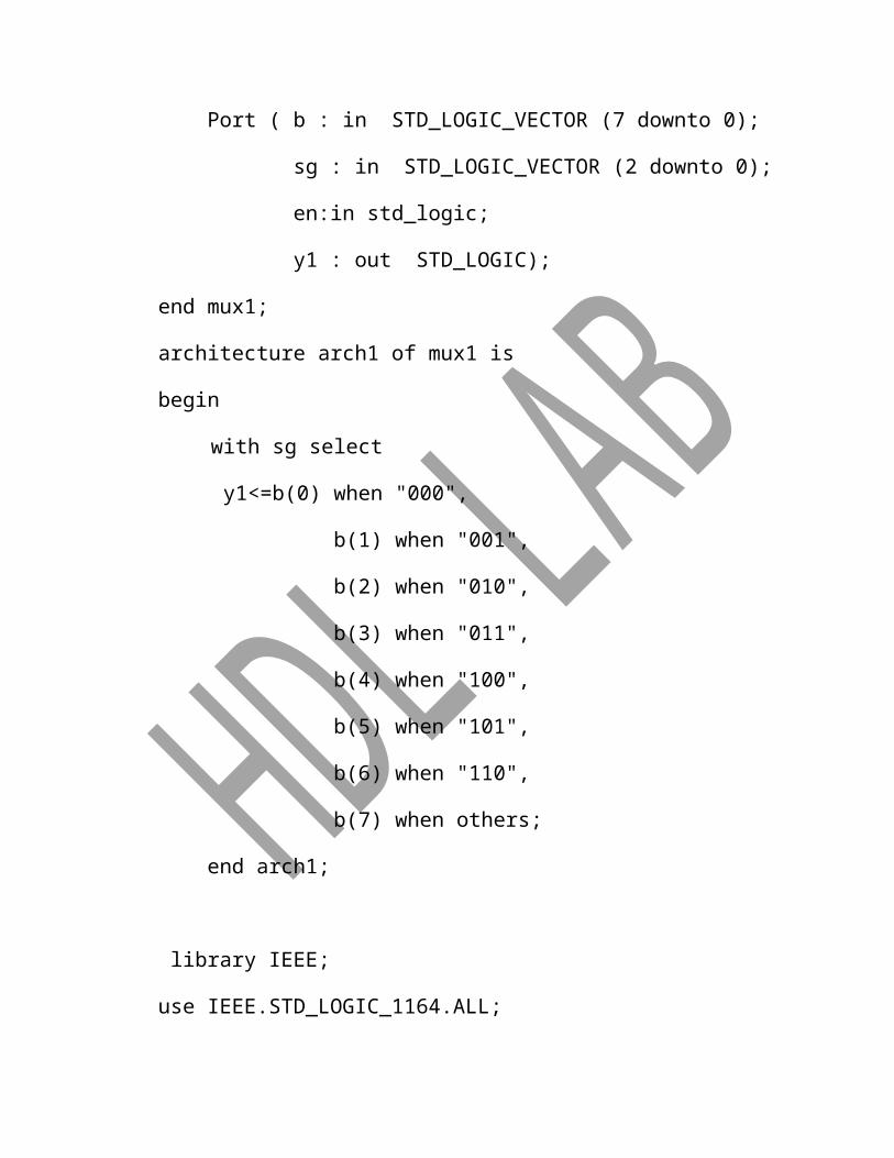
Port ( b : in STD_LOGIC_VECTOR (7 downto 0);
sg : in STD_LOGIC_VECTOR (2 downto 0);
en:in std_logic;
y1 : out STD_LOGIC);
end mux1;
architecture arch1 of mux1 is
begin
with sg select
y1<=b(0) when "000",
b(1) when "001",
b(2) when "010",
b(3) when "011",
b(4) when "100",
b(5) when "101",
b(6) when "110",
b(7) when others;

end arch1;
library IEEE;
use IEEE.STD_LOGIC_1164.ALL;
entity not1 is
port(l:in std_logic;
m:out std_logic);
end not1;
architecture arch2 of not1 is
begin
m <=not l ;
end arch2;
library IEEE;
use IEEE.STD_LOGIC_1164.ALL;
entity or1 is
port(d,e:in std_logic;
f:out std_logic);
end or1;
architecture arch3 of or1 is
begin
f<=d or e;
end arch3;
6. TIMING DIAGRAMS :-
The timing diagrams of 16x1 multiplexer is shown in figure 6.1
FIGURE 6.1: timing diagram of 16x1 multiplexer
7. FINAL SYNTHESIS REPORT :-
Final Results:
RTL Top Level Output File Name : muxer.ngr
Top Level Output File Name : muxer
Output Format : NGC
Optimization Goal : Speed
Keep Hierarchy : NO
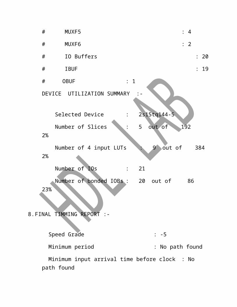
Design Statistics:
# IOs : 21
Cell Usage :
# BELS : 15
# LUT2 : 1
# LUT3 : 8
# MUXF5 : 4
# MUXF6 : 2

# IO Buffers : 20
# IBUF : 19
# OBUF : 1
DEVICE UTILIZATION SUMMARY :-
Selected Device : 2s15tq144-5
Number of Slices : 5 out of 192 2%
Number of 4 input LUTs : 9 out of 384 2%
Number of IOs : 21
Number of bonded IOBs : 20 out of 86 23%
8. FINAL TIMMING REPORT :-
Speed Grade : -5
Minimum period : No path found
Minimum input arrival time before clock : No path found
Maximum output required time after clock : No path found
Maximum combinational path delay : 12.888ns
9. RESULTS AND CONCLUSIONS:-
Hence 16x1 multiplexer was simulated and synthesized by using Xilinx software.

EXPERIMENT-2
74X381
4-BIT
ALU
74x381 4-bit alu
1. AIM :-
To simulate and synthesize 74x381 4-bit ALU using Xilinx software.
2. SOFTWARE USED :-
XST(Xilinx Synthesis Tool) for synthesis and
ModelSim simulator for simulation.
3. INTRODUCTION :-
An ALU (Arithmetic and Logical Unit) is a combinational circuit that can
perform any of a number of different arithmetic and logical operations on a pair
of b-bit operands. The operation to be performed is specified by a set of
function-select inputs.
Typical MSI ALUs have 4-bit operands and three to five function-select inputs,
allowing upto 32 different functions to be performed. There are three MSI
ALUs. They are 74x181, 74x381 & 74x382. They encode their select inputs
more compactly, and provide only eight different but useful functions.
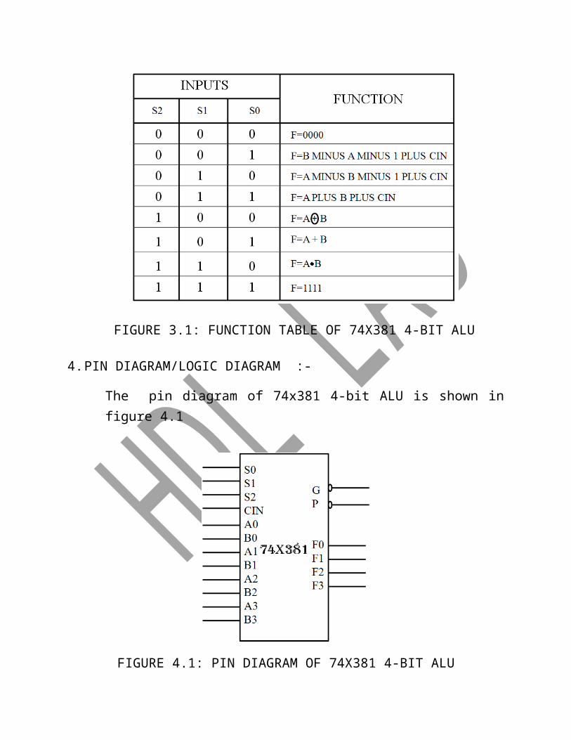
The functions performed by 74x381 and 74x382 4-bit ALUs are shown in
figure 3.1. The only difference between the 74x381 and 74x382 is that one
provides group carry look ahead outputs, while the other provides ripple carry
and overflow outputs. The Cin input of least significant ALU is normally set to
zero during addition operations.

FIGURE 3.1: FUNCTION TABLE OF 74X381 4-BIT ALU
4. PIN DIAGRAM/LOGIC DIAGRAM :-
The pin diagram of 74x381 4-bit ALU is shown in figure 4.1
FIGURE 4.1: PIN DIAGRAM OF 74X381 4-BIT ALU
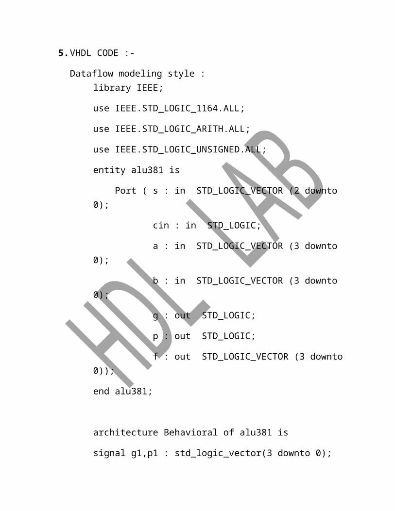
5. VHDL CODE :-
Dataflow modeling style :library IEEE;
use IEEE.STD_LOGIC_1164.ALL;
use IEEE.STD_LOGIC_ARITH.ALL;
use IEEE.STD_LOGIC_UNSIGNED.ALL;
entity alu381 is
Port ( s : in STD_LOGIC_VECTOR (2 downto 0);
cin : in STD_LOGIC;
a : in STD_LOGIC_VECTOR (3 downto 0);
b : in STD_LOGIC_VECTOR (3 downto 0);
g : out STD_LOGIC;
p : out STD_LOGIC;
f : out STD_LOGIC_VECTOR (3 downto 0));
end alu381;
architecture Behavioral of alu381 is
signal g1,p1 : std_logic_vector(3 downto 0);
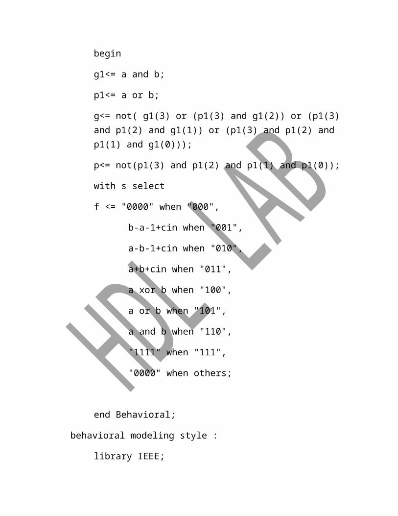
begin
g1<= a and b;
p1<= a or b;
g<= not( g1(3) or (p1(3) and g1(2)) or (p1(3) and p1(2) and g1(1)) or (p1(3) and p1(2) and p1(1) and g1(0)));
p<= not(p1(3) and p1(2) and p1(1) and p1(0));
with s select
f <= "0000" when "000",
b-a-1+cin when "001",
a-b-1+cin when "010",
a+b+cin when "011",
a xor b when "100",
a or b when "101",
a and b when "110",
"1111" when "111",
"0000" when others;
end Behavioral;
behavioral modeling style :
library IEEE;
use IEEE.STD_LOGIC_1164.ALL;
use IEEE.STD_LOGIC_ARITH.ALL;
use IEEE.STD_LOGIC_UNSIGNED.ALL;
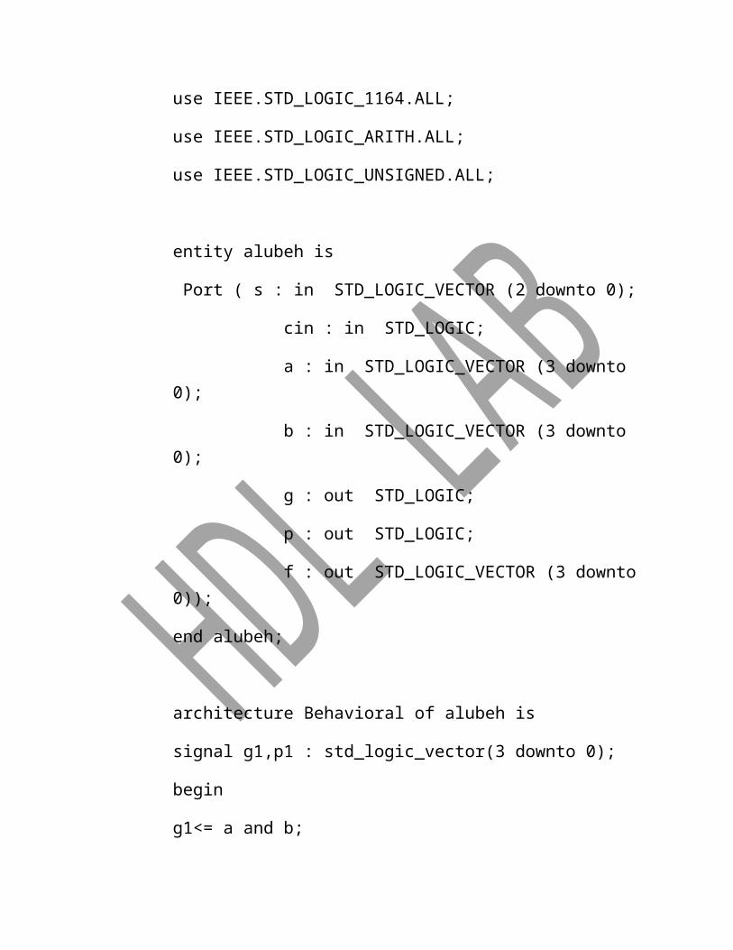
entity alubeh is
Port ( s : in STD_LOGIC_VECTOR (2 downto 0);
cin : in STD_LOGIC;
a : in STD_LOGIC_VECTOR (3 downto 0);
b : in STD_LOGIC_VECTOR (3 downto 0);
g : out STD_LOGIC;
p : out STD_LOGIC;
f : out STD_LOGIC_VECTOR (3 downto 0));
end alubeh;
architecture Behavioral of alubeh is
signal g1,p1 : std_logic_vector(3 downto 0);
begin
g1<= a and b;
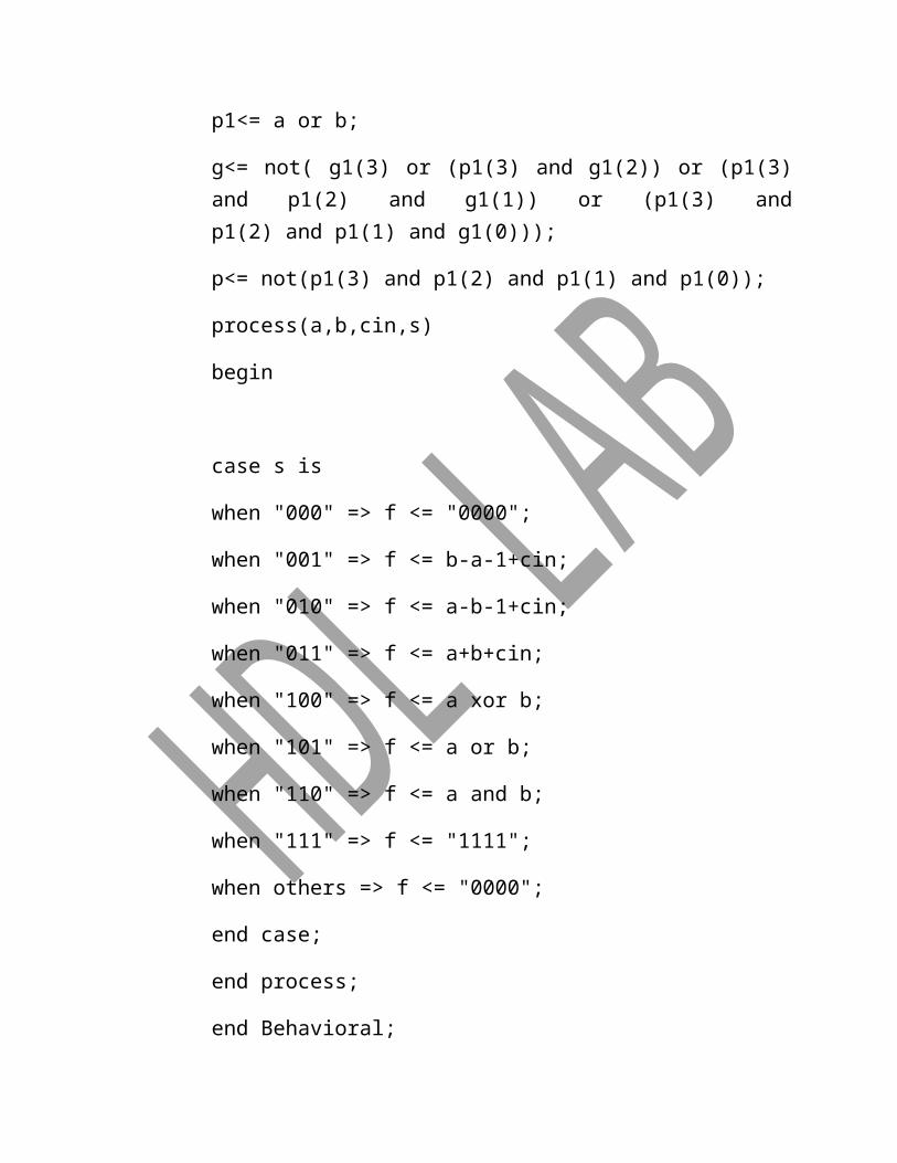
p1<= a or b;
g<= not( g1(3) or (p1(3) and g1(2)) or (p1(3) and p1(2) and g1(1)) or (p1(3) and p1(2) and p1(1) and g1(0)));
p<= not(p1(3) and p1(2) and p1(1) and p1(0));
process(a,b,cin,s)
begin
case s is
when "000" => f <= "0000";
when "001" => f <= b-a-1+cin;
when "010" => f <= a-b-1+cin;
when "011" => f <= a+b+cin;
when "100" => f <= a xor b;
when "101" => f <= a or b;
when "110" => f <= a and b;
when "111" => f <= "1111";
when others => f <= "0000";
end case;
end process;
end Behavioral;
6. TIMING DIAGRAMS :-
The timing diagram of 74x381 4-bit ALU is shown in figure 6.1 .
FIGURE 6.1: timing diagram of 74x381 4-bit ALU
7. FINAL SYNTHESIS REPORT :-
Final Results:
RTL Top Level Output File Name : alubeh.ngr
Top Level Output File Name : alubeh
Output Format : NGC
Optimization Goal : Speed
Keep Hierarchy : NO
Design Statistics:
# IOs : 18
Cell Usage :
# BELS : 47
# LUT2 : 5
# LUT3 : 11
# LUT4 : 17
# MULT_AND : 2
# MUXCY : 3
# MUXF5 : 5
# XORCY : 4
# IO Buffers : 18
# IBUF : 12
# OBUF : 6
DEVICE UTILIZATION SUMMARY :-
Selected Device : 3s100evq100-5
Number of Slices : 19 out of 960 1%
Number of 4 input LUTs : 33 out of 1920 1%
Number of IOs : 18
Number of bonded IOBs : 18 out of 66 27%
8. FINAL TIMMING REPORT :-
Speed Grade : -5
Minimum period : No path found
Minimum input arrival time before clock : No path found
Maximum output required time after clock : No path found
Maximum combinational path delay : 12.902ns
9. RESULTS AND CONCLUSIONS:-
Hence 74x381 4-bit ALU was simulated and synthesized using Xilinx software.
EXPERIMENT-3
UP
DOWN
COUNTER
Up down counter

1. AIM :-
To simulate and synthesize the 8-bit up/down counter using Xilinx software.
2. SOFTWARE USED :-
XST(Xilinx Synthesis Tool) for synthesis and
ModelSim simulator for simulation.
3. INTRODUCTION :-Counter is generally used for any clocked sequential circuit whose state diagram contains a single cycle as shown in figure 3.1. The modulus of a counter is the number of states in the cycle. A counter with m states is called a modulo-m counter or sometimes a divide by m counter. A counter with a non-power of 2 modulus has extra states that are not used in normal operation. The most commonly used counter type is an n-bit binary counter. Such a counter has n flip-flops and has 2n states.
There are two types of counters. They are.
1. Asynchronous counter.2. Synchronous counter.
The asynchronous counter has a disadvantage in so far as the unwanted spikes are concerned. This limitation is overcome by parallel counter. Synchronous counters are faster than asynchronous counters because the propagation delay is less. A counter may be up counter or a down counter. An up counter is a counter which counts in the upward direction. A down counter is a counter which counts in the downward direction. Both operations can be done by a single counter called up/down counter. This operation can be done by a select pin and is called up/down pin. When up/down=1 the counter counts the upward direction and when 0 the counter counts the downward direction.
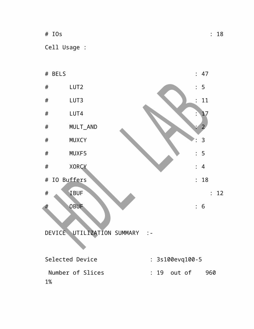
FIGURE 3.1: GENERAL STRUCTURE OF A COUNTER STATE DIAGRAM
4. PIN DIAGRAM/LOGIC DIAGRAM :-
The pin diagram of up/down counter is shown in figure 4.1
The logic diagram of up/down counter is shown in figure 4.2
FIGURE 4.1: PIN DIAGRAM OF 8-BIT UP/DOWN COUNTER
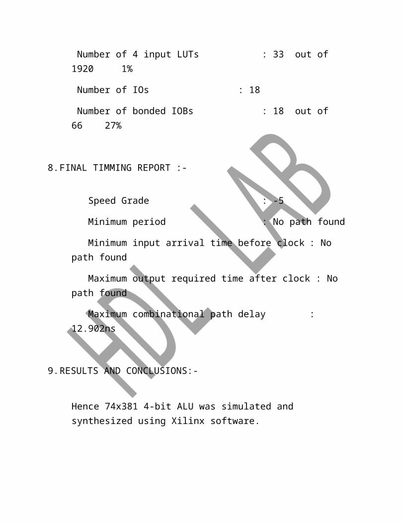
FIGURE 4.2: LOGIC DIAGRAM OF 8-BIT UP/DOWN COUNTER USING
JK FLIPFLOPS
5. VHDL CODE :-
Behavioral modeling style :
library IEEE;
use IEEE.STD_LOGIC_1164.ALL;
use IEEE.STD_LOGIC_ARITH.ALL;
use IEEE.STD_LOGIC_UNSIGNED.ALL;
entity udcounter is
Port ( rst : in STD_LOGIC;
clk : in STD_LOGIC;

up_down : in STD_LOGIC;
a : inout STD_LOGIC_VECTOR (7 downto 0));
end udcounter;
architecture Behavioral of udcounter is
begin
process(rst,clk,up_down)
begin
if(rst='1')then
a<= "00000000";
elsif (clk'event and clk ='1') then
if (up_down = '1') then
if ( a="11111111") then
a<= "00000000";
else
a<= a+'1';
end if;
elsif (up_down = '0') then
if ( a="00000000") then
a<= "11111111";
else
a<= a-'1';

end if;
end if;
end if;
end process;
end Behavioral;
6. TIMING DIAGRAMS :-
The timing diagram of 8-bit up/down counter is shown in figure 6.1
FIGURE 6.1: timing diagram of 8-BIT UP/DOWN COUNTER
7. FINAL SYNTHESIS REPORT :-
Final Results:
RTL Top Level Output File Name : udcounter.ngr
Top Level Output File Name : udcounter
Output Format : NGC
Optimization Goal : Speed
Keep Hierarchy : NO
Design Statistics:
# IOs : 11
Cell Usage :
# BELS : 13
# INV : 1
# LUT3 : 4
# LUT3_D : 2
# LUT4 : 4
# LUT4_L : 2
# FlipFlops/Latches : 8
# FDC : 8
# Clock Buffers : 1
# BUFGP : 1
# IO Buffers : 10
# IBUF : 2
# OBUF : 8
DEVICE UTILIZATION SUMMARY :
Selected Device : 3s100evq100-5
Number of Slices : 6 out of 960 0%
Number of Slice Flip Flops : 8 out of 1920 0%

Number of 4 input LUTs : 3 out of 1920 0%
Number of IOs : 11
Number of bonded IOBs : 11 out of 66 16%
Number of GCLKs : 1 out of 24 4%
8. FINAL TIMMING REPORT :-
Speed Grade : -5
Minimum period: 3.103ns (Maximum Frequency : 322.279MHz)
Minimum input arrival time before clock : 3.922ns
Maximum output required time after clock : 4.221ns
Maximum combinational path delay : No path found
9. Results and conclusions :-
Hence 8-bit up/down counter was simulated and synthesized using Xilinx software.
EXPERIMENT-4
32X8
ROM
32x8 rom
1. AIM :-
To simulate and synthesize 32x8 ROM using Xilinx software.
2. SOFTWARE USED :-
XST(Xilinx Synthesis Tool) for synthesis and
ModelSim simulator for simulation.
3. INTRODUCTION :-
A Read Only Memory (ROM) is essentially a memory device in which permanent binary information is stored. The binary information must be specified by the designer and is then embedded into the unit from the required interconnection pattern. Once the pattern is established, it stays within the unit when the power is turned off and on again. As the name suggests it is meant only for reading the information from it. A block diagram of ROM is shown in figure 3.1. it consists of K inputs and N outputs. The inputs provided the address of the memory and the output gives the data bits of the stored word which is selected by the address. The number of words in a ROM is determined from the fact that K address input lines are needed to specify 2k words. Note that ROM doesn’t have data input because it doesn’t have a write operation.
In general a “2k x n” ROM will have an internal “k x 2k” decoder and n OR gates. Each of the OR gates has 2k inputs, which are connected to each of the output of the decoder.
32x8 ROM consists of 32 words of 8-bit each. There are 5 input lines that form the binary numbers from 0 through 31 for the address. The 32 outputs of the decoder are connected to each of the 8 OR gates. Each OR gate must be considered as having 32 inputs. Each output of the decoder is connected to one of the inputs of each OR gate. Since each OR gate has 32 inputs connecting and there are 8 OR gates, the ROM contains 32x8=256 connections.

FIGURE 3.1: BLOCK DIAGRAM OF ROM
4. PIN DIAGRAM/LOGIC DIAGRAM :-
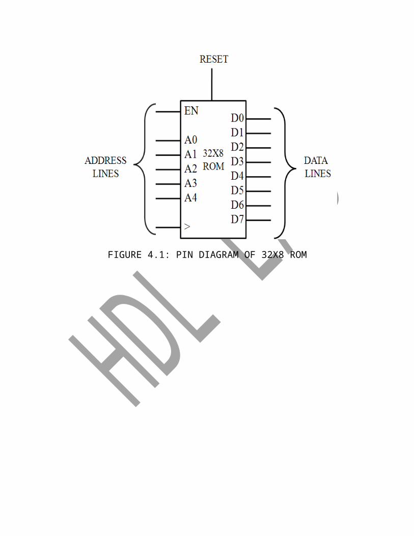
A. The pin diagram of 32x8 ROM is shown in figure 4.1
B. The logic diagram of 32x8 ROM is shown in figure 4.2
FIGURE 4.1: PIN DIAGRAM OF 32X8 ROM
FIGURE 4.2: LOGIC DIAGRAM OF 32X8 ROM
5. VHDL CODE :-
Behavioral modeling style :
library IEEE;
use IEEE.STD_LOGIC_1164.ALL;
use IEEE.STD_LOGIC_ARITH.ALL;
use IEEE.STD_LOGIC_UNSIGNED.ALL;
entity rom32x8 is

Port ( reset : in STD_LOGIC;
clk : in STD_LOGIC;
read1 : in STD_LOGIC;
en : in STD_LOGIC;
a : in STD_LOGIC_VECTOR (4 downto 0);
dataout : out STD_LOGIC_VECTOR (7 downto 0));
end rom32x8;
architecture Behavioral of rom32x8 is
type rom_array is array(0 to 31) of STD_LOGIC_VECTOR (7 downto 0);
constant content : rom_array :=
(0=> "00000001",
1=> "00000010",
2=> "00000011",
3=> "00000100",
4=> "00000101",
5=> "00000110",
6=> "00000111",
7=> "00001000",
8=> "00001001",
9=> "00001010",
10=> "00001011",
11=> "00001100",

12=> "00001101",
13=> "00001110",
14=> "00001111",
others=> "11111111");
begin
process (reset,en,clk,read1)
begin
if (reset = '1') then
dataout <= "00000000";
elsif (clk'event and clk='1')then
if ( en = '1') then
if(read1 = '1') then
dataout <= content(conv_integer(a));
end if;
end if;
end if;
end process;
end Behavioral;

6. TIMING DIAGRAMS :-
The timing diagram of 32x8 ROM is shown in figure 6.1 .
FIGURE 6.1: timing diagram of 32X8 ROM
7. FINAL SYNTHESIS REPORT :-
Final Results:
RTL Top Level Output File Name : rom32x8.ngr
Top Level Output File Name : rom32x8
Output Format : NGC
Optimization Goal : Speed
Keep Hierarchy : NO
Design Statistics:
# IOs : 17
Cell Usage :
# BELS : 11
# LUT2 : 1
# LUT3 : 3
# LUT4 : 3
# MUXF5 : 3
# VCC : 1
# FlipFlops/Latches : 8
# FDCE : 8
# Clock Buffers : 1
# BUFGP : 1
# IO Buffers : 16
# IBUF : 8
# OBUF : 8
DEVICE UTILIZATION SUMMARY :
Selected Device : 3s100evq100-5
Number of Slices : 4 out of 960 0%
Number of Slice Flip Flops : 8 out of 1920 0%
Number of 4 input LUTs : 7 out of 1920 0%
Number of IOs : 17
Number of bonded IOBs : 17 out of 66 25%
IOB Flip Flops : 8
Number of GCLKs : 1 out of 24 4%

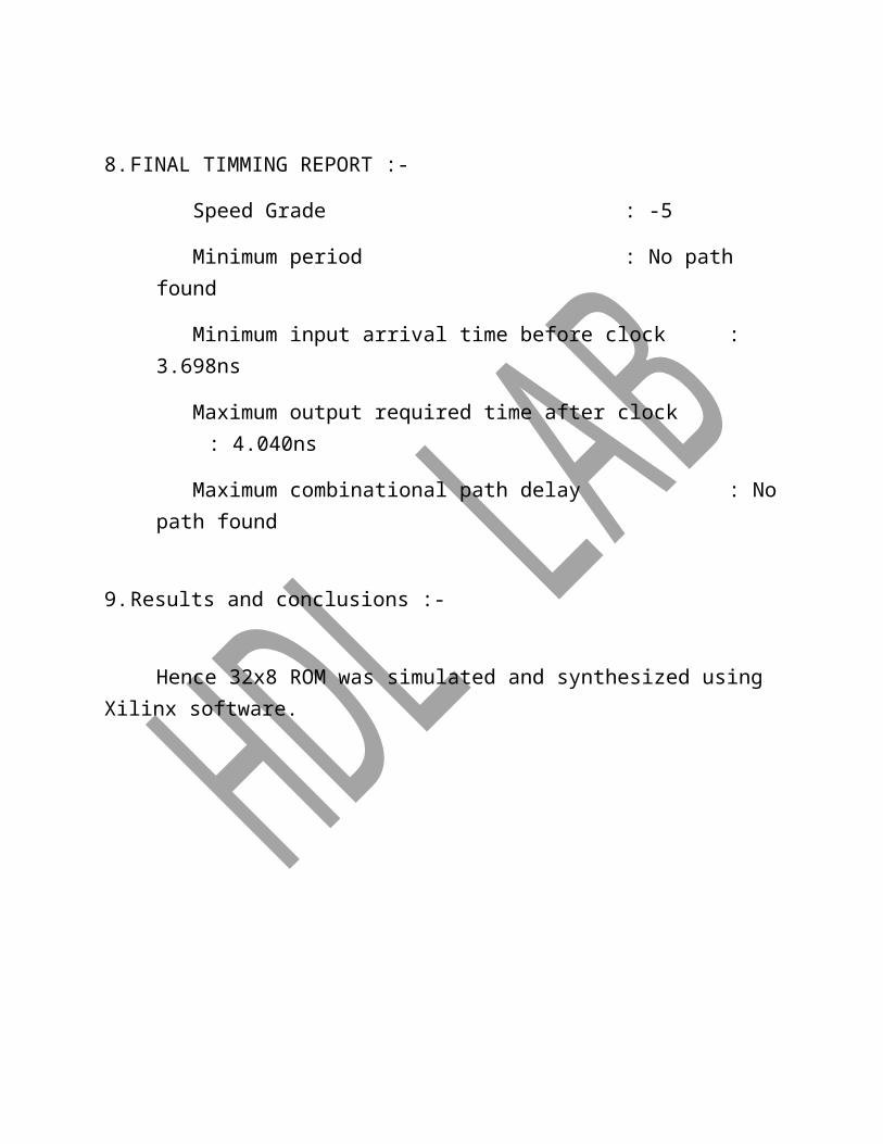
8. FINAL TIMMING REPORT :-
Speed Grade : -5
Minimum period : No path found
Minimum input arrival time before clock : 3.698ns
Maximum output required time after clock : 4.040ns
Maximum combinational path delay : No path found
9. Results and conclusions :-
Hence 32x8 ROM was simulated and synthesized using Xilinx software.

EXPERIMENT-5
SEQUENCE
DETECTOR
101
Sequence detector 101
1. AIM :-
To simulate and synthesize sequence detector 101 using Xilinx software.
2. SOFTWARE USED :-
XST(Xilinx Synthesis Tool) for synthesis and
ModelSim simulator for simulation.
3. INTRODUCTION :-
Clocked synchronous state machine is generic name given to feedback sequential circuits. “Clocked” refer to the fact that their storage elements (flip-flops) employ a clock input and “synchronous” means that all the flipflops use the same clock signal. Such a state machine changes state only when a triggering edge or tick occurs on the clock signal.
A finite state machine is an abstract model that describes the synchronous sequential machine. Since it is a sequential circuit the output depends on the present input as well as on the past inputs,(i.e.) on the past histories and since a machine might have an infinite varieties of possible histories, it would need an infinite capacity for storing them. Since it is impossible to implement machines which have infinite storage capabilities, we consider only finite state machines.
The block diagram of mealy circuit is shown in figure 3.1. The mealy model consists of D- flipflops.

FIGURE 3.1: BASIC MEALY MODEL CIRCUIT
4. PIN DIAGRAM/LOGIC DIAGRAM :-
A. The state diagram of mealy model is shown in figure 4.1
B. The state table of mealy model is shown in figure 4.2
FIGURE 4.1: STATE DIAGRAM OF SEQUENCE DETECTOR
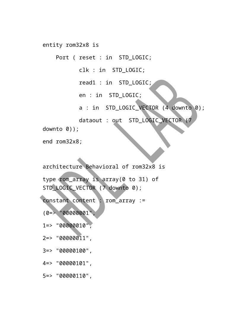
FIGURE 4.2: STATE TABLE OF SEQUENCE DETECTOR 101
5. VHDL CODE :-
Behavioral modeling style :
library IEEE;
use IEEE.STD_LOGIC_1164.ALL;
use IEEE.STD_LOGIC_ARITH.ALL;
use IEEE.STD_LOGIC_UNSIGNED.ALL;
entity seqd is
Port ( a : in STD_LOGIC;
clk : in STD_LOGIC;
z : out STD_LOGIC);
end seqd;
architecture Behavioral of seqd is
type mealy_type is (s0,s1,s2);
signal pstate,nstate: mealy_type;
begin

process(clk)
begin
if (clk='1') then
pstate <= nstate;
end if;
end process;
process(pstate,a)
begin
case pstate is
when s0 =>
if a='1' then
z<= '0';
nstate<= s1;
else
z<='0';
end if;
when s1=>
if a='0' then
z<= '0';
nstate<= s2;
else
z<='0';
end if;

when s2 =>
if a='1' then
z<= '1';
nstate<= s0;
else
z<='0';
nstate<= s0;
end if;
when others=>
nstate<= s0;
end case;
end process;
end Behavioral;
6. TIMING DIAGRAMS :-
The timing diagram of sequence detector 101 is shown in figure 6.1.
FIGURE 6.1: timing diagram of SEQUENCE DETECTOR 101

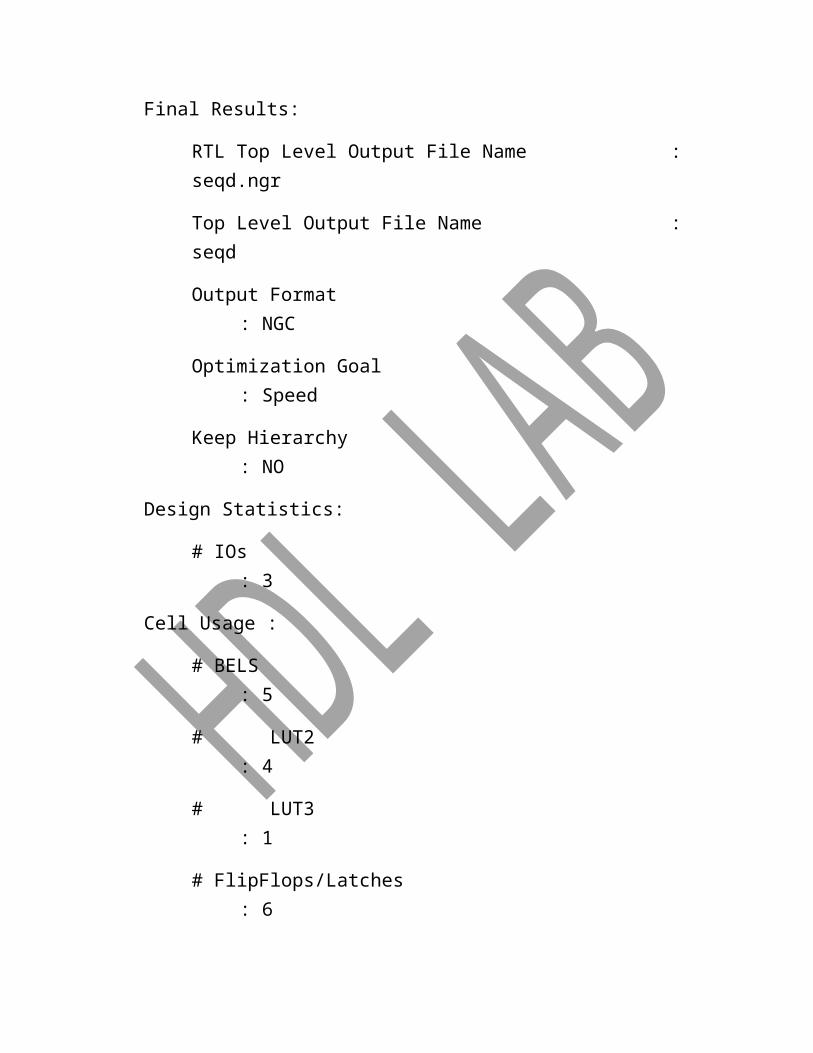
7. FINAL SYNTHESIS REPORT :-
Final Results:
RTL Top Level Output File Name : seqd.ngr
Top Level Output File Name : seqd
Output Format : NGC
Optimization Goal : Speed
Keep Hierarchy : NO
Design Statistics:
# IOs : 3
Cell Usage :
# BELS : 5
# LUT2 : 4
# LUT3 : 1
# FlipFlops/Latches : 6
# LD : 6
# Clock Buffers : 1
# BUFGP : 1
# IO Buffers : 2
# IBUF : 1
# OBUF : 1
DEVICE UTILIZATION SUMMARY :

Selected Device : 3s100evq100-5
Number of Slices : 3 out of 960 0%
Number of Slice Flip Flops : 6 out of 1920 0%
Number of 4 input LUTs : 5 out of 1920 0%
Number of IOs : 3
Number of bonded IOBs : 3 out of 66 4%
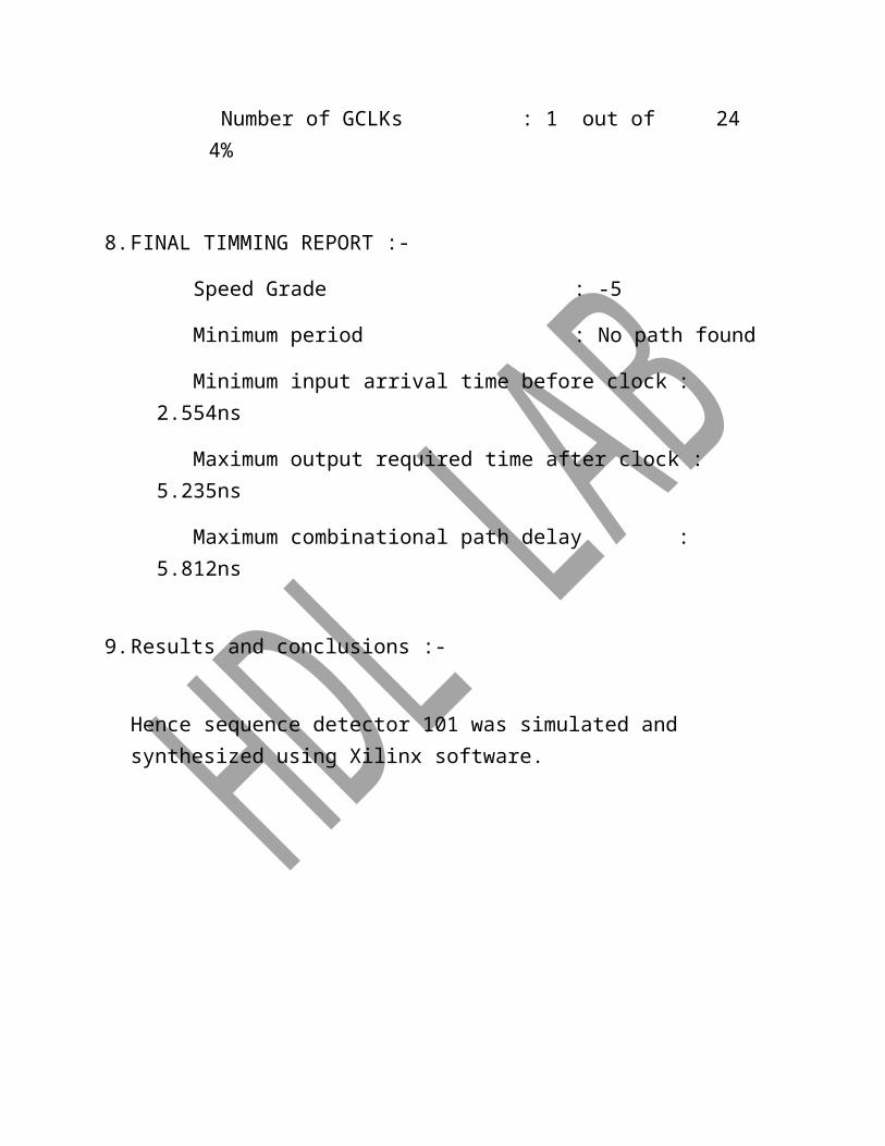
Number of GCLKs : 1 out of 24 4%
8. FINAL TIMMING REPORT :-
Speed Grade : -5
Minimum period : No path found
Minimum input arrival time before clock : 2.554ns
Maximum output required time after clock : 5.235ns
Maximum combinational path delay : 5.812ns
9. Results and conclusions :-
Hence sequence detector 101 was simulated and synthesized using Xilinx software.
Verilog
coding
EXPERIMENT-6
DECODERS
decoders

1. AIM :-
A. To simulate and synthesize 2 to 4 decoder using Xilinx software.
B. To simulate and synthesize 3 to 8 decoder with 2 to 4 decoder using Xilinx software.
C. To simulate and synthesize 4 to 16 decoder with 3 to 8 decoder using Xilinx software.
2. SOFTWARE USED :-
Cadence nclaunch for simulation and
Cadence encounter rc complier for synthesis.
3. INTRODUCTION :-
A decoder is a multiple input, multiple output logic circuit that converts coded inputs into coded outputs, where the inputs and output codes are different. The input code generally has fewer bits than the output code, and there is a one to one mapping from input code words into output code words. In a one to one mapping, each input code words into output code words. The most commonly used input code is an n-bit binary code, where an n-bit word represents one of 2n different coded values, normally the integers from 0 through 2n -1. Sometimes an n-bit binary code is truncated to represent fewer than 2n values.
The most commonly used output code is a 1 out of m code, which contains m bits, where one bit is asserted at any time.
The most commonly used decoder circuit is an n to 2n decoder or binary decoder. Such a decoder has an n bit binary input code and a 1 out of 2n output code. A binary decoder is used when you need to activate exactly one of 2n
outputs based on an n bit input value.

4. PIN DIAGRAM/LOGIC DIAGRAM :-
A. The logic diagram of 2 to 4 decoder is shown in figure 4.1
B. The logic diagram of 3 to 8 decoder using 2 to 4 decoder is shown in figure 4.2
C. The logic diagram of 4 to 16 decoder using 3 to 8 decoder is shown in figure 4.3
FIGURE 4.1: LOGIC DIAGRAM OF 2TO4 DECODER
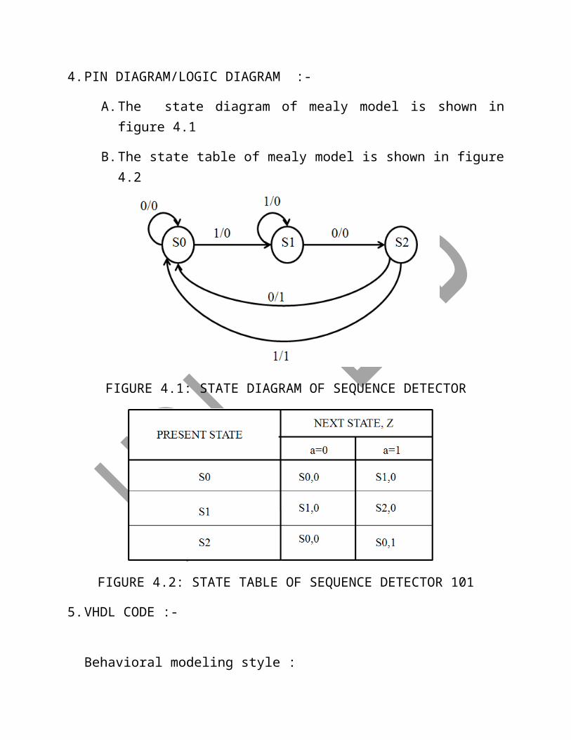
FIGURE 4.2: LOGIC DIAGRAM OF 3TO8 DECODER
FIGURE 43: LOGIC DIAGRAM OF 4TO16 DECODER

5. Verilog CODE :-
A. 2 to 4 decoder:-
module decoder2to4(a, b,en); input en;
input [1:0] a; output [3:0] b;
wire [1:0]aa;not (aa[0],a[0]),(aa[1],a[1]);and (b[0],aa[0],aa[1],en),
(b[2],aa[0],a[1],en),(b[1],a[0],aa[1],en),(b[3],a[0],a[1],en);
endmodule
module test_decoder2to4(); reg en; reg [1:0] a;
wire [3:0] b; decoder2to4 dec1(a, b,en); initial begin {en,a}=3'b000;
#2 {en,a}=3'b100;#2 {en,a}=3'b101;
#2 {en,a}=3'b110;#2 {en,a}=3'b111;
end initial $monitor($time,"en=%b,a=%b,b=%b",en,a,b); initial #10 $stop;
endmodule

module decoder3to8(q, pp, enn); input [2:0] q; output [7:0] pp; input enn;
wire qq; wire [7:0] p; not (qq,q[2]); decoder2to4 g1 (.b(p[3:0]),.a(q[1:0]),.en(qq)); decoder2to4 g2 (.b(p[7:4]),.a(q[1:0]),.en(q[2])); and (pp[0],p[0],enn),
(pp[1],p[1],enn),(pp[2],p[2],enn),(pp[3],p[3],enn),(pp[4],p[4],enn),(pp[5],p[5],enn),(pp[6],p[6],enn),(pp[7],p[7],enn);
endmodule
module test_decoder3to8();reg[2:0] q;wire [7:0] pp;reg enn;decoder3to8 dec2(q, pp, enn);initial begin {enn,q}=4'b0000;
#2 {enn,q}=4'b1000;#2 {enn,q}=4'b1001;
#2 {enn,q}=4'b1010;#2 {enn,q}=4'b1011;#2 {enn,q}=4'b1100;#2 {enn,q}=4'b1101;#2 {enn,q}=4'b1110;#2 {enn,q}=4'b1111;

end initial $monitor($time,"enn=%b,q=%b,pp=%b",enn,q,pp); initial #20 $stop;
endmodule
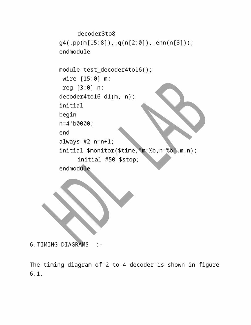
module decoder4to16(m, n); output [15:0] m; input [3:0] n;
wire nn; not (nn,n[3]); decoder3to8 g3(.pp(m[7:0]),.q(n[2:0]),.enn(nn)); decoder3to8 g4(.pp(m[15:8]),.q(n[2:0]),.enn(n[3]));
endmodule
module test_decoder4to16(); wire [15:0] m; reg [3:0] n;decoder4to16 d1(m, n);initialbeginn=4'b0000;endalways #2 n=n+1;initial $monitor($time,"m=%b,n=%b",m,n);
initial #50 $stop;endmodule
6. TIMING DIAGRAMS :-
The timing diagram of 2 to 4 decoder is shown in figure 6.1.
FIGURE 6.1: timing diagram of 2TO4 DECODER
The timing diagram of 3 to 8 decoder is shown in figure 6.2.
FIGURE 6.2: timing diagram of 3TO8 DECODER
The timing diagram of 4 to 16 decoder is shown in figure 6.3.
FIGURE 6.3: timing diagram of 4TO16 DECODER
7. FINAL SYNTHESIS REPORT :-
2to4 decoder:-
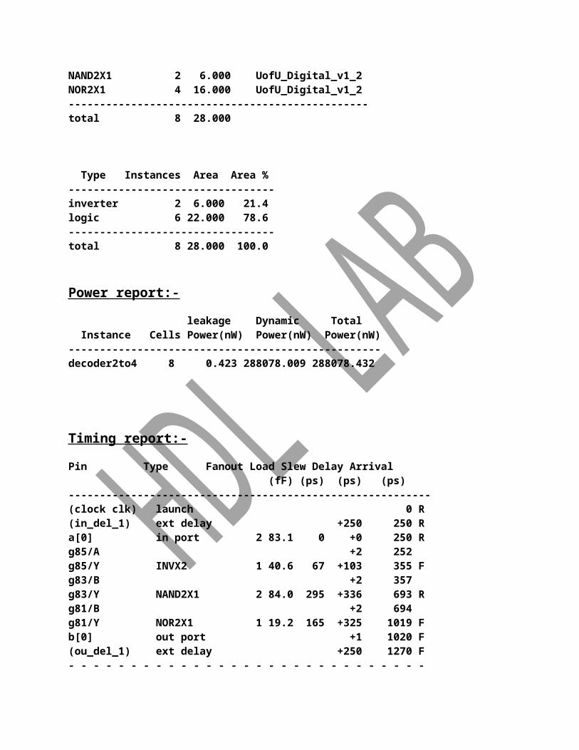
Cell report:-Gate Instances Area Library ------------------------------------------------INVX2 2 6.000 UofU_Digital_v1_2

NAND2X1 2 6.000 UofU_Digital_v1_2 NOR2X1 4 16.000 UofU_Digital_v1_2 ------------------------------------------------total 8 28.000
Type Instances Area Area % ---------------------------------inverter 2 6.000 21.4 logic 6 22.000 78.6 ---------------------------------total 8 28.000 100.0
Power report:-
leakage Dynamic Total Instance Cells Power(nW) Power(nW) Power(nW) --------------------------------------------------decoder2to4 8 0.423 288078.009 288078.432
Timing report:-
Pin Type Fanout Load Slew Delay Arrival (fF) (ps) (ps) (ps) ----------------------------------------------------------(clock clk) launch 0 R (in_del_1) ext delay +250 250 R a[0] in port 2 83.1 0 +0 250 R g85/A +2 252 g85/Y INVX2 1 40.6 67 +103 355 F g83/B +2 357 g83/Y NAND2X1 2 84.0 295 +336 693 R g81/B +2 694 g81/Y NOR2X1 1 19.2 165 +325 1019 F b[0] out port +1 1020 F (ou_del_1) ext delay +250 1270 F - - - - - - - - - - - - - - - - - - - - - - - - - - - - - (clock clk) capture 10000 R ----------------------------------------------------------Timing slack : 8730ps Start-point : a[0]End-point : b[0]
3to8 decoder:-
Cell report:- Gate Instances Area Library ------------------------------------------------INVX1 1 3.000 UofU_Digital_v1_2 INVX2 8 24.000 UofU_Digital_v1_2 NAND2X1 8 24.000 UofU_Digital_v1_2 ------------------------------------------------total 17 51.000
Type Instances Area Area % -----------------------------------inverter 9 27.000 52.9 unresolved 2 0.000 0.0 logic 8 24.000 47.1 -----------------------------------total 19 51.000 100.0
Power report:-
Leakage Dynamic Total Instance Cells Power(nW) Power(nW) Power(nW) --------------------------------------------------decoder3to8 17 0.764 501417.267 501418.031 g1 0 0.000 54800.000 54800.000 g2 0 0.000 66000.000 66000.000
Timing report:-
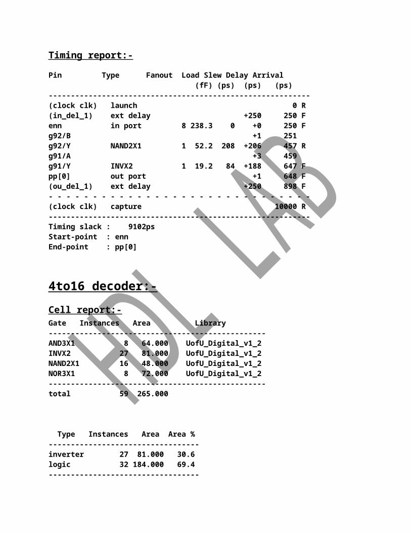
Pin Type Fanout Load Slew Delay Arrival (fF) (ps) (ps) (ps) -----------------------------------------------------------(clock clk) launch 0 R (in_del_1) ext delay +250 250 F enn in port 8 238.3 0 +0 250 F g92/B +1 251 g92/Y NAND2X1 1 52.2 208 +206 457 R g91/A +3 459 g91/Y INVX2 1 19.2 84 +188 647 F pp[0] out port +1 648 F (ou_del_1) ext delay +250 898 F - - - - - - - - - - - - - - - - - - - - - - - - - - - - - -(clock clk) capture 10000 R
-----------------------------------------------------------Timing slack : 9102ps Start-point : ennEnd-point : pp[0]
4to16 decoder:-
Cell report:-Gate Instances Area Library -------------------------------------------------AND3X1 8 64.000 UofU_Digital_v1_2 INVX2 27 81.000 UofU_Digital_v1_2 NAND2X1 16 48.000 UofU_Digital_v1_2 NOR3X1 8 72.000 UofU_Digital_v1_2 -------------------------------------------------total 59 265.000
Type Instances Area Area % ----------------------------------inverter 27 81.000 30.6 logic 32 184.000 69.4 ----------------------------------total 59 265.000 100.0
Power report:-
Leakage Dynamic Total Instance Cells Power(nW) Power(nW) Power(nW) -----------------------------------------------------decoder4to16 59 4.077 2018280.979 2018285.056 g3 29 2.021 711049.292 711051.314 g1 6 0.628 264481.442 264482.071 g2 6 0.628 246308.181 246308.809 g4 29 2.021 806371.781 806373.802 g1 6 0.628 264481.442 264482.071 g2 6 0.628 246308.181 246308.809
Timing report:-
Pin Type Fanout Load Slew Delay Arrival (fF) (ps) (ps) (ps) -----------------------------------------------------------(clock clk) launch 0 R (in_del_1) ext delay +250 250 R n[2] in port 8 306.3 0 +0 250 R g3/q[2]
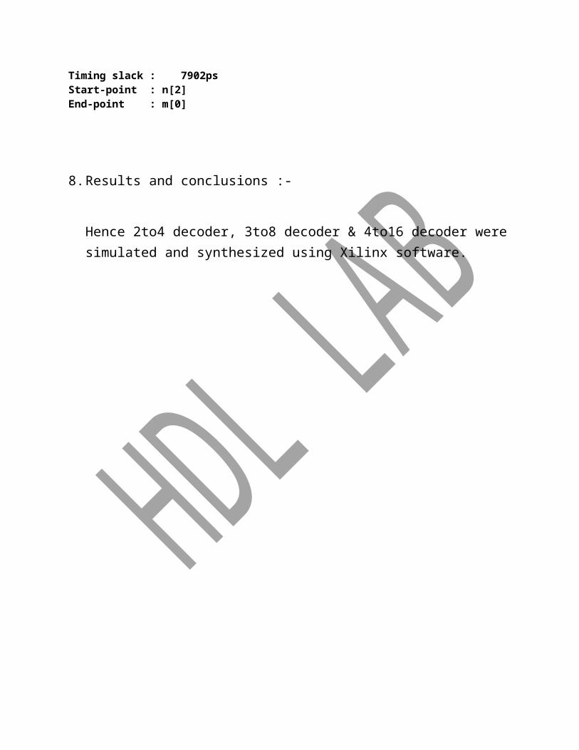
g12/A +1 251 g12/Y INVX2 3 124.9 184 +225 476 F g1/en g73/A +2 478 g73/Y INVX2 2 106.0 174 +294 772 R g69/C +2 774 g69/Y NOR3X1 1 40.6 429 +377 1151 F g1/b[0] g67/B +2 1153 g67/Y NAND2X1 1 52.2 238 +489 1642 R g66/A +3 1645 g66/Y INVX2 1 19.2 92 +203 1847 F g3/pp[0] m[0] out port +1 1848 F (ou_del_1) ext delay +250 2098 F - - - - - - - - - - - - - - - - - - - - - - - - - - - - - -(clock clk) capture 10000 R -----------------------------------------------------------Timing slack : 7902ps Start-point : n[2]End-point : m[0]
8. Results and conclusions :-
Hence 2to4 decoder, 3to8 decoder & 4to16 decoder were simulated and synthesized using Xilinx software.
EXPERIMENT-7
SHIFT
REGISTER
Shift register
1. AIM :-
To simulate and synthesize shift register using Xilinx software.
2. SOFTWARE USED :-
Cadence nclaunch for simulation and Cadence encounter rc complier for synthesis.
3. INTRODUCTION :-
A shift register is an n-bit register with a provision for shifting its stored data by one bit position at each tick of the clock. In a shift register group of flipflops are arranged so that the binary numbers stored in the flipflops are shifted from one flipflop to the next for every clock pulse.
As shown in figure 4.1 shift register has two inputs where one is clock and the other is r_l which controls the left and right shift operations. It is an 8-bit shift register and hence output is of 8-bit size. Here at the negative edge of clock, the output is shifted either left or right based on r_l. if r_l=’0’, ‘a’ is shifted left by one bit and operator used in verilog for shift is “<<N” where it shifts left N bits. If r_l=’1’, ‘a’ is shifted right by one bit and operator for right shift in verilog is “>>N” where it shifts right N bits.
4. PIN DIAGRAM/LOGIC DIAGRAM :-
The logic diagram of shift register is shown in figure 4.1
FIGURE 4.1: LOGIC DIAGRAM OF SHIFT REGISTER

5. verilog CODE :-
module shiftreg(clk, r_l, a); input clk; input r_l; output [7:0] a;
reg [7:0] a; initial a=8'h01; always @(negedge clk) begin a=(r_l)? (a>>1'b1): (a<<1'b1); end
endmodule
module test_shiftreg(); reg clk;
reg r_l; wire [7:0] a;
shiftreg sr1(clk, r_l, a); initial begin clk=1'b1; r_l=1'b0; end always #2 clk=~clk; always #8 r_l=~r_l; initial $monitor ($time,"clk=%b,r_l=%b,a=%b",clk,r_l,a); initial #30 $stop;
endmodule

6. TIMING DIAGRAMS :-
The timing diagram of 8-bit shift register is shown in figure 6.1.
FIGURE 6.1: timing diagram of SHIFT REGISTER
7. FINAL SYNTHESIS REPORT :-
cell report:-
Gate Instances Area Library -------------------------------------------------DCBNX1 8 144.000 UofU_Digital_v1_2 INVX2 1 3.000 UofU_Digital_v1_2 MUX2X2 6 54.000 UofU_Digital_v1_2 NAND2X1 1 3.000 UofU_Digital_v1_2 NOR2X1 1 4.000 UofU_Digital_v1_2 -------------------------------------------------total 17 208.000
Type Instances Area Area % ------------------------------------sequential 8 144.000 69.2 inverter 1 3.000 1.4 logic 8 61.000 29.3 ------------------------------------total 17 208.000 100.0
power report:-
Leakage Dynamic Total Instance Cells Power(nW) Power(nW) Power(nW) -------------------------------------------------

shiftreg 17 5.081 5939371.788 5939376.869
timing report:-
Pin Type Fanout Load Slew Delay Arrival (fF) (ps) (ps) (ps) -----------------------------------------------------------(clock clk) launch 5000 F a_reg[2]/CLK 400 5000 F a_reg[2]/Q DCBNX1 3 92.7 476 +1607 6607 F a[2] out port +0 6608 F (ou_del_1) ext delay +250 6858 F - - - - - - - - - - - - - - - - - - - - - - - - - - - - - -(clock clk) capture 10000 R -----------------------------------------------------------Timing slack : 3142ps Start-point : a_reg[2]/CLKEnd-point : a[2]
8. Results and conclusions :-
Hence shift register was simulated and synthesized using Xilinx software.
EXPERIMENT-8
BCD

ADDER
Bcd adder
1. AIM :-
To simulate and synthesize 4-bit BCD adder using Xilinx software.
2. SOFTWARE USED :-
Cadence nclaunch for simulation and
Cadence encounter rc complier for synthesis..
3. INTRODUCTION :-
The 8421 BCD code is widely used and it is a common practice to refer to it as BCD code. In this code each decimal digit that is 0 through 9 is coded by a 4 bit

binary number. It is also called the natural binary code because of the 8,4,2,1 weights attached to it. Only 10 combinations in BCD are possible i.e. 0000 to 1001 where are the combinations 1010, 1011, 1100, 1101, 1110, 1111 are not possible.
The BCD addition is performed by individually adding the corresponding digits of the decimal numbers expressed in 4-bit binary group starting from LSB. If there is no carry and sum is in between 0000 to 1001, no correction is needed. If there is a carry out of one group to next group or if the sum term is in between 1010 to 1111, then 6 i.e. 0110 is added to the sum term of that group and the resulting carry is added to the sum term of that group to the next group. BCD adder is used for this purpose. In verilog, the logic can be written through a compact assignment using a ternary operator. The assignment statement has the form
Assign { co, sum } = { sum<=4’b1001}?{1’b0,sumb}:{sumb+4’b0110};
4. PIN DIAGRAM/LOGIC DIAGRAM :-
The logic diagram of 4 bit BCD adder is shown in figure 4.1
FIGURE 4.1: LOGIC DIAGRAM OF 4-BIT BCD ADDER
5. Verilog CODE :-
module bcdadd(a, b, sum, co);
input [3:0] a; input [3:0] b; output [3:0] sum; output co;
wire [3:0]sumb; assign sumb=a+b; assign {co,sum}= (sumb<=4'b1001)?{1'b0,sumb}:(sumb+4'b0110);
endmodule
module test_bcdadd();reg [3:0] a;
reg [3:0] b; wire [3:0] sum; wire co;
bcdadd b1(a, b, sum, co);initial begin a=4'h0;b=4'h0;endalways #2 a=a+2;always #2 b=b+4;initial $monitor ($time,"a=%b,b=%b,sum=%b,co=%b",a,b,sum,co);initial #20 $stop;
endmodule
6. TIMING DIAGRAMS :- The timing diagram for BCD adder is shown in figure 6.1.

FIGURE 6.1: timing diagram of BCD ADDER
7. FINAL SYNTHESIS REPORT :-
cell report:-
Gate Instances Area Library -------------------------------------------------AOI21X1 2 10.000 UofU_Digital_v1_2 INVX2 1 3.000 UofU_Digital_v1_2 NAND2X1 3 9.000 UofU_Digital_v1_2 NOR2X1 3 12.000 UofU_Digital_v1_2 OAI21X1 2 10.000 UofU_Digital_v1_2 XNOR2X1 5 40.000 UofU_Digital_v1_2 XOR2X1 3 24.000 UofU_Digital_v1_2 -------------------------------------------------total 19 108.000
Type Instances Area Area % ----------------------------------inverter 1 3.000 2.8 logic 18 105.000 97.2 ----------------------------------total 19 108.000 100.0
power report:-
Leakage Dynamic Total Instance Cells Power(nW) Power(nW) Power(nW) -------------------------------------------------bcdadd 19 2.174 1959920.816 1959922.989
timing report:-
Pin Type Fanout Load Slew Delay Arrival (fF) (ps) (ps) (ps) -----------------------------------------------------------(clock clk) launch 0 R (in_del_1) ext delay +250 250 R b[1] in port 3 128.9 0 +0 250 R g371/A +1 251 g371/Y NOR2X1 1 52.0 264 +335 586 F g365/A +3 589 g365/Y OAI21X1 2 105.1 409 +545 1134 R g364/A +2 1136 g364/Y INVX2 1 52.0 168 +338 1474 F g359/A +3 1477 g359/Y OAI21X1 1 62.5 296 +381 1858 R g2/B +3 1861 g2/Y XOR2X1 2 83.3 403 +706 2567 R g356/C +2 2568 g356/Y AOI21X1 4 146.3 530 +829 3397 F g354/B +2 3399 g354/Y XNOR2X1 1 19.2 252 +541 3940 F sum[1] out port +1 3941 F (ou_del_1) ext delay +250 4191 F - - - - - - - - - - - - - - - - - - - - - - - - - - - - - -(clock clk) capture 10000 R -----------------------------------------------------------Timing slack : 5809ps Start-point : b[1]End-point : sum[1]
8. Results and conclusions :-
Hence BCD adder was simulated and synthesized using Xilinx software.

EXPERIMENT-9
PARITY
CHECKER
Parity checker
1. AIM :-
To simulate and synthesize the 8 bit parity checker using Xilinx software.
2. SOFTWARE USED :-
Cadence nclaunch for simulation and Cadence encounter rc complier for synthesis.
3. INTRODUCTION :-
The simplest technique for detecting errors is that of adding an extra bit, known as parity bit. To each word being transmitted, there are two types of parity. One is odd parity and the other is even parity. For odd parity, the parity bit is set to ‘0’ or ‘1’ at the transmitter such that the total number of ‘1’ bits in the word including the parity bit is an odd number.
For even parity, the parity is set to ‘0’ or ‘1’ at the transmitter such that the total number of ‘1’ bits in the word including the parity bit is an even number. Figure 3.1 shows daisy chain connection .

FIGURE 3.1: DAISY CHAIN CONNECTION OF PARITY CHECKER
4. PIN DIAGRAM/LOGIC DIAGRAM :-
The logic diagram of 8 bit odd parity checker is shown in figure 4.1.
FIGURE 4.1: LOGIC DIAGRAM OF8-BIT PARITY CHECKER
5. Verilog CODE :-
module parity_chk(a, en, chk); input [7:0] a; input en; output chk;
reg chk;
wire [7:0]a; always@(posedge en) begin
chk = pb(a);$display("t=%0d,a=%b,en=%0b,pb=%0b",$time,a,en,chk);
end function pb; input [7:0]a;
pb=^a; endfunction
endmodule
module test_parity_chk();
reg [7:0]a;reg en;wire chk;integer i;parity_chk p1(a,en,chk);initial #0 en=1'b0;always #2 en=~en;initial begin
#1 a=8'h00;for (i=0;i<8;i=i+1)begin
#4 a=a+3'o6;end
endinitial #40 $stop;
endmodule
6. TIMING DIAGRAMS :-

The timing diagram of parity checker is shown in figure 6.1.
FIGURE 6.1: timing diagram of parity checker
7. FINAL SYNTHESIS REPORT :-
cell report:-
Gate Instances Area Library -----------------------------------------------DCBX1 1 18.000 UofU_Digital_v1_2 XOR2X1 7 56.000 UofU_Digital_v1_2 -----------------------------------------------total 8 74.000
Type Instances Area Area % -----------------------------------sequential 1 18.000 24.3 logic 7 56.000 75.7 -----------------------------------total 8 74.000 100.0
power report:-
Leakage Dynamic Total Instance Cells Power(nW) Power(nW) Power(nW) ---------------------------------------------------parity_chk 8 1.769 2250740.776 2250742.545
timing report:-
Pin Type Fanout Load Slew Delay Arrival (fF) (ps) (ps) (ps) ----------------------------------------------------------(clock clk) launch 0 R (in_del_1) ext delay +250 250 R a[1] in port 1 61.7 0 +0 250 R g73/A +3 253 g73/Y XOR2X1 1 61.7 329 +492 745 R g68/A +3 748 g68/Y XOR2X1 1 61.7 334 +669 1418 R g67/A +3 1421 g67/Y XOR2X1 1 45.6 286 +618 2039 R chk_reg/D DCBX1 +2 2041 chk_reg/CLK setup 400 +34 2075 R - - - - - - - - - - - - - - - - - - - - - - - - - - - - - (clock clk) capture 10000 R ----------------------------------------------------------Timing slack : 7925ps Start-point : a[1]End-point : chk_reg/D
8. Results and conclusions :-
Hence 8-bit parity checker was simulated and synthesized using Xilinx software.

EXPERIMENT-10
SEQUENCE
GENERATOR
Sequence generator
1. AIM :-
To simulate and synthesize the sequence generator moore model using Xilinx software.
2. SOFTWARE USED :-
Cadence nclaunch for simulation and Cadence encounter rc complier for synthesis.
3. INTRODUCTION :-
A pulse generator or sequence generator is a system which generates a prescribed clock. These pulse trains or sequence of bits can be used to open values, turn on lights, turn off machines or perform any of a variety of jobs. Pulse trains can be generated using either direct logic or indirect logic. In direct logic the output taken from flipflop’s, where as in indirect logic, it is taken from a decoder gates.
Here, sequence generated is to have four binary outputs designed w, x, y, z. These are to follow either of two sequences depending on the value of a Boolean variable.
The sequence to be followed is
1000-> 1100->0100-> 0110-> 0010-> 0011-> 0001-> 1001-> 1000
This is shown in figure 3.1.
FIGURE 3.1: STATE DIAGRAM OF SEQUENCE GENERATOR
4. PIN DIAGRAM/LOGIC DIAGRAM :-
The logic diagram of sequence generator is shown in figure 4.1
FIGURE 4.1: LOGIC DIAGRAM OF SEQUENCE GENERATOR
5. Verilog CODE :-
`define s0 3'b000
`define s1 3'b001
`define s2 3'b010
`define s3 3'b011
`define s4 3'b100
`define s5 3'b101
`define s6 3'b110
`define s7 3'b111
module a_seqmoorev(clk,clr,w,x,y,z);
input clk;
input clr;
output w,x,y,z;
reg w,x,y,z;
reg [2:0] present_state;
always@(present_state)
begin
case (present_state)
`s0: {w,x,y,z}=4'b1000;
`s1: {w,x,y,z}=4'b1100;
`s2: {w,x,y,z}=4'b0100;
`s3: {w,x,y,z}=4'b0110;
`s4: {w,x,y,z}=4'b0010;
`s5: {w,x,y,z}=4'b0011;
`s6: {w,x,y,z}=4'b0001;
`s7: {w,x,y,z}=4'b1001;
endcase
end
always@(posedge clk)
begin
if(clr) present_state=`s0;
else
begin
case(present_state)
`s0:present_state=`s1;
`s1:present_state=`s2;
`s2:present_state=`s3;
`s3:present_state=`s4;
`s4:present_state=`s5;
`s5:present_state=`s6;
`s6:present_state=`s7;
`s7:present_state=`s0;
default:present_state=`s0;
endcase
end
end
endmodule
module test_a_seqmoorev();
reg clk,clr;
wire w,x,y,z;
a_seqmoorev al(clk,clr,w,x,y,z);
initial
begin
clk=1'b0;
clr=1'b1;
#3 clr=1'b0;
end
always #2 clk=~clk;
initial #50 $stop;
endmodule
6. TIMING DIAGRAMS :- The timing diagram of sequence generator is shown in figure 6.1.
FIGURE 6.1: timing diagram of sequence generator
7. FINAL SYNTHESIS REPORT :-
cell report:-
Gate Instances Area Library -------------------------------------------------AOI21X1 1 5.000 UofU_Digital_v1_2 DCBX1 3 54.000 UofU_Digital_v1_2 MUX2NX1 2 14.000 UofU_Digital_v1_2 NAND2X1 1 3.000 UofU_Digital_v1_2 NOR2X1 6 24.000 UofU_Digital_v1_2 XOR2X1 1 8.000 UofU_Digital_v1_2 -------------------------------------------------total 14 108.000
Type Instances Area Area % ------------------------------------sequential 3 54.000 50.0 logic 11 54.000 50.0 ------------------------------------total 14 108.000 100.0
power report:-
Leakage Dynamic Total Instance Cells Power(nW) Power(nW) Power(nW) ----------------------------------------------------a_seqmoorev 14 2.330 2640024.865 2640027.195
timing report:-
Pin Type Fanout Load Slew Delay Arrival (fF) (ps) (ps) (ps) ----------------------------------------------------------------------(clock clk) launch 0 R present_state_reg[1]/CLK 400 0 R present_state_reg[1]/Q DCBX1 5 193.8 820 +2090 2090 F g200/B +1 2091 g200/Y NAND2X1 2 83.2 382 +832 2923 R g193/A +2 2925 g193/Y MUX2NX1 2 56.4 321 +432 3357 F
g191/C +2 3359 g191/Y AOI21X1 1 46.8 331 +402 3761 R g189/B +2 3763 g189/Y NOR2X1 1 45.7 245 +435 4198 F present_state_reg[2]/D DCBX1 +2 4200 present_state_reg[2]/CLK setup 400 +263 4463 R - - - - - - - - - - - - - - - - - - - - - - - - - - - - - - - - - - - (clock clk) capture 10000 R ----------------------------------------------------------------------Timing slack : 5537ps Start-point : present_state_reg[1]/CLKEnd-point : present_state_reg[2]/D
8. Results and conclusions :-
Hence sequence generator was simulated and synthesized using Xilinx software.