c3d08065e v = 650 v silicon carbide schottky diode rrm i ... · 1 c3d65e rev. a, 12215 c3d08065e...
TRANSCRIPT
1 C3D08065E Rev. A, 12-2015
C3D08065ESilicon Carbide Schottky Diode
Z-Rec® Rectifier
Features
• 650-VoltSchottkyRectifier• ZeroReverseRecoveryCurrent• ZeroForwardRecoveryVoltage• High-FrequencyOperation• Temperature-IndependentSwitchingBehavior• ExtremelyFastSwitching• PositiveTemperatureCoefficientonVF
Benefits
• ReplaceBipolarwithUnipolarRectifiers• EssentiallyNoSwitchingLosses• HigherEfficiency• ReductionofHeatSinkRequirements• ParallelDevicesWithoutThermalRunaway
Applications
• SwitchModePowerSupplies • PowerFactorCorrection• MotorDrives
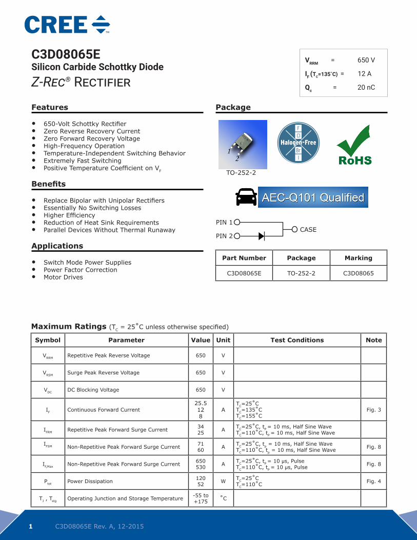
Package
TO-252-2
Maximum Ratings (TC=25˚Cunlessotherwisespecified)
Symbol Parameter Value Unit Test Conditions Note
VRRM RepetitivePeakReverseVoltage 650 V
VRSM SurgePeakReverseVoltage 650 V
VDC DCBlockingVoltage 650 V
IF ContinuousForwardCurrent25.5128
ATC=25˚CTC=135˚CTC=155˚C
Fig.3
IFRM RepetitivePeakForwardSurgeCurrent 3425 A TC=25˚C,tP=10ms,HalfSineWave
TC=110˚C,tP=10ms,HalfSineWave
IFSM Non-RepetitivePeakForwardSurgeCurrent 7160 A TC=25˚C,tp=10ms,HalfSineWave
TC=110˚C,tp=10ms,HalfSineWaveFig.8
IF,Max Non-RepetitivePeakForwardSurgeCurrent 650530 A TC=25˚C,tP=10µs,Pulse
TC=110˚C,tP=10µs,PulseFig.8
Ptot PowerDissipation 12052 W TC=25˚C
TC=110˚CFig.4
TJ,Tstg OperatingJunctionandStorageTemperature -55to+175 ˚C
Part Number Package Marking
C3D08065E TO-252-2 C3D08065
VRRM = 650 V
IF (TC=135˚C) = 12 A
Qc = 20 nC
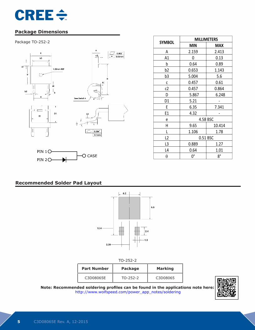
PIN1
PIN2CASE

2 C3D08065E Rev. A, 12-2015
10
15
20
25
30
Re
ve
rse
Le
ak
ag
e C
urr
en
t, I
RR
(mA
)
TJ = 175 °C
TJ = 125 °C
TJ = 75 °C
T = 25 °C
0
5
10
0 100 200 300 400 500 600 700 800 900 1000
Re
ve
rse
Le
ak
ag
e C
urr
en
t, I
Reverse Voltage, VR (V)
TJ = -55 °C
TJ = 25 °C
Electrical Characteristics
Symbol Parameter Typ. Max. Unit Test Conditions Note
VF ForwardVoltage 1.52.1
1.82.4 V IF=8ATJ=25°C
IF=8ATJ=175°CFig.1
IR ReverseCurrent 1020
50200 μA VR=650VTJ=25°C
VR=650VTJ=175°CFig.2
QC TotalCapacitiveCharge 20 nCVR=650V,IF=8Adi/dt=500A/μsTJ=25°C
Fig.5
C TotalCapacitance3953732
pFVR=0V,TJ=25°C,f=1MHzVR=200V,TJ=25˚C,f=1MHzVR=400V,TJ=25˚C,f=1MHz
Fig.6
EC CapacitanceStoredEnergy 3.0 μJ VR=400V Fig.7
Note:Thisisamajoritycarrierdiode,sothereisnoreverserecoverycharge.
Thermal Characteristics
Symbol Parameter Typ. Unit Note
RθJC ThermalResistancefromJunctiontoCase 1.25 °C/W Fig.9
Typical Performance
Figure1.ForwardCharacteristics Figure2.ReverseCharacteristics
020040060080010001200
8
10
12
14
16
18
20
Fow
ard
Cu
rren
t, I F
(A)
TJ = -55 °C
TJ = 25 °C
TJ = 75 °C
TJ = 175 °C
TJ = 125 °C
0
2
4
6
0.0 0.5 1.0 1.5 2.0 2.5 3.0 3.5 4.0
Fow
ard
Cu
rren
t, I
Foward Voltage, VF (V)
I F (
A)
VF (V) VR (V)
I R (
mA)

3 C3D08065E Rev. A, 12-2015
30
40
50
60
70
80
90
I F(A
)
10% Duty20% Duty30% Duty50% Duty70% DutyDC
0
10
20
30
25 50 75 100 125 150 175
TC (°C)
Figure3.CurrentDerating Figure4.PowerDerating
60
80
100
120
140
PTOT(W
)0
20
40
25 50 75 100 125 150 175
TC (°C)
Figure5.TotalCapacitanceChargevs.ReverseVoltage Figure6.Capacitancevs.ReverseVoltage
Typical Performance
10
15
20
25
30
Ca
pa
citi
ve
Ch
arg
e,
QC
(nC
)
Conditions:TJ = 25 °C
0
5
10
0 100 200 300 400 500 600 700
Ca
pa
citi
ve
Ch
arg
e,
Q
Reverse Voltage, VR (V)
150
200
250
300
350
400
450
Ca
pa
cita
nce
(p
F)
Conditions:TJ = 25 °CFtest = 1 MHzVtest = 25 mV
0
50
100
150
0 1 10 100 1000
Ca
pa
cita
nce
(p
F)
Reverse Voltage, VR (V)
I F(p
eak)
(A
)
TC ˚C TC ˚C
PTo
t (W
)C
(p
F)
VR (V)
QC (
nC
)
VR (V)

4 C3D08065E Rev. A, 12-2015
3
4
5
6
7
8
Ca
pa
cita
nce
Sto
red
En
erg
y, E
C( µµ µµ
J)
0
1
2
0 100 200 300 400 500 600 700
Ca
pa
cita
nce
Sto
red
En
erg
y, E
Reverse Voltage, VR (V)
Typical Performance
100
1,000
I FS
M(A
)
TJ = 25 °CTJ = 110 °C
1010E-6 100E-6 1E-3 10E-3
Time, tp (s)
Figure7.CapacitanceStoredEnergy Figure8.Non-repetitivepeakforwardsurgecurrentversuspulseduration(sinusoidalwaveform)
tp (s)
I FS
M (
A)
VR (V)
E C(m
J)
Figure9.TransientThermalImpedance
100E-3
1
Ther
mal
Res
istan
ce (
o C/W
)
0.5
0.3
0.1
0.05
0.02
0.01
SinglePulse
1E-3
10E-3
1E-6 10E-6 100E-6 1E-3 10E-3 100E-3 1Time, tp (s)
0.01
Ther
mal
Res
ista
nce
(˚
C/
W)
T (Sec)
5 C3D08065E Rev. A, 12-2015
Recommended Solder Pad Layout
Part Number Package Marking
C3D08065E TO-252-2 C3D08065
Note: Recommended soldering profiles can be found in the applications note here: http://www.wolfspeed.com/power_app_notes/soldering
Package Dimensions
PackageTO-252-2
Tjb June 2015 MX+DI+PSI
TO-252-2
SYMBOL MILLIMETERSMIN MAX
A 2.159 2.413A1 0 0.13b 0.64 0.89
b2 0.653 1.143b3 5.004 5.6c 0.457 0.61
c2 0.457 0.864D 5.867 6.248
D1 5.21 -E 6.35 7.341
E1 4.32 -e 4.58 BSC H 9.65 10.414L 1.106 1.78
L2 0.51 BSC L3 0.889 1.27L4 0.64 1.01θ 0° 8°
Tjb June 2015 MX+DI+PSI

66 C3D08065E Rev. A, 12-2015
Copyright © 2015 Cree, Inc. All rights reserved. The information in this document is subject to change without notice. Cree, the Cree logo, and Zero Recovery are registered trademarks of Cree, Inc.
Cree, Inc.4600 Silicon Drive
Durham, NC 27703USA Tel: +1.919.313.5300
Fax: +1.919.313.5451www.cree.com/power
• RoHSCompliance The levels of RoHS restricted materials in this product are below the maximum concentration values (also referred to as the threshold limits) permitted for such substances, or are used in an exempted application, in accordance with EU Directive 2011/65/EC (RoHS2), as implemented January 2, 2013. RoHS Declarations for this product can be obtained from your Wolfspeed representative or from the Product Ecology section of our website at http://www.wolfspeed.com/power/tools-and-support/product-ecology.
• REAChCompliance REACh substances of high concern (SVHCs) information is available for this product. Since the European Chemi-cal Agency (ECHA) has published notice of their intent to frequently revise the SVHC listing for the foreseeable future,please contact a Cree representative to insure you get the most up-to-date REACh SVHC Declaration. REACh banned substance information (REACh Article 67) is also available upon request.
• This product has not been designed or tested for use in, and is not intended for use in, applications implanted into the human body nor in applications in which failure of the product could lead to death, personal injury or property damage, including but not limited to equipment used in the operation of nuclear facilities, life-support machines, cardiacdefibrillatorsorsimilaremergencymedicalequipment,aircraftnavigationorcommunicationorcontrolsystems,orairtrafficcontrolsystems.
Notes
• Cree SiC Schottky diode portfolio: http://www.wolfspeed.com/Power/Products#SiCSchottkyDiodes• Schottky diode Spice models: http://www.wolfspeed.com/power/tools-and-support/DIODE-model-request2• SiC MOSFET and diode reference designs: http://go.pardot.com/l/101562/2015-07-31/349i
RelatedLinks
Diode Model
VT RT
Diode Model CSD04060
Vf T = VT + If*RT
VT= 0.965 + (Tj * -1.3*10-3) RT= 0.096 + (Tj * 1.06*10-3)
Note: Tj = Diode Junction Temperature In Degrees Celsius, valid from 25°C to 175°C
VfT=VT+If*RT
VT=0.95+(TJ*-1.2*10-3)RT=0.054+(TJ*5.5*10-4)