c10lp nios ii hello world lab manual - intel
TRANSCRIPT
©2017 Intel Corporation. All rights reserved. ALTERA, ARRIA, CYCLONE, HARDCOPY, INTEL, MAX, MEGACORE, NIOS, QUARTUS and STRATIX words and logos are trademarks of Intel Corporation and registered in the U.S. Patent and Trademark Office and in other countries. All other words and logos identified as trademarks or service marks are the property of their respective holders as described at www.altera.com/common/legal.html. Intel warrants performance of its semiconductor products to current specifications in accordance with Intel's standard warranty, but reserves the right to make changes to any products and services at any time without notice. Intel assumes no responsibility or liability arising out of the application or use of any information, product, or service described herein except as expressly agreed to in writing by Intel. Intel customers are advised to obtain the latest version of device specifications before relying on any published information and before placing orders for products or services.
Date: 8/25/2017
Revision: 1.0
Cyclone 10 LP Nios II ‘Hello World’ Lab Manual
2
Table of Contents Theory of operation ........................................................................................3 Hardware and software Requirements.......................................................... 3 Build the Qsys based processor system .............................................................4
Build the top level design ............................................................................. 13 Add the Nios II system into design ....................................... ………………..15 Creating the software for the “Hello World” design............................................18
Downloading the Hardware Image ................................................................23 Run the Nios II Software ....................................................................…........24 Summary...................................................................................................... .25 Revision and History ......................................................................................26
3
Theory of Operation This lab showcases how to create an embedded system in programmable logic using Intel’s “soft” Nios II processor.
In this design, the Nios II processor load a program that prints “Hello World” to the screen. This requires a working processor to execute the code, on-chip memory to store the software executable, a JTAG UART peripheral to send the “Hello World” text to a terminal. To make the lab a little bit more interesting and hardware-centric, we will utilize the push button switches and LEDs to allow interaction with the development kit. The lab is split into Hardware Section and Software Section
Hardware and Software Requirements The reference design requires the following hardware and software to run the test: • Quartus® Prime Software Version: 17.0 • Cyclone 10 LP FPGA Evaluation Kit
To directly use this reference design:
1) Download this design ‘C10LP_NiosII_hello_world.par’ from Design Store. 2) Open the .par in Quartus Prime 17.0.0 Standard Edition. 3) Close the project, then rename the design from ‘C10LP_NiosII_hello_world_project’ to
‘C10LP_NiosII_hello_world’. 4) Unzip the ‘software.zip’ folder, and copy the ‘software’ folder in this project main
directory. 5) Re-open the project in Quartus Prime, perform compilation, then download the .sof into
dev kit. 6) Next, follow the steps in section ‘SOFTWARE DESIGN’ on this document to build the
Nios II and run the test.
4
HARDWARE DESIGN
Build the Qsys based processor system
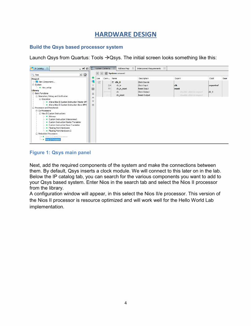
Launch Qsys from Quartus: Tools Qsys. The initial screen looks something like this:
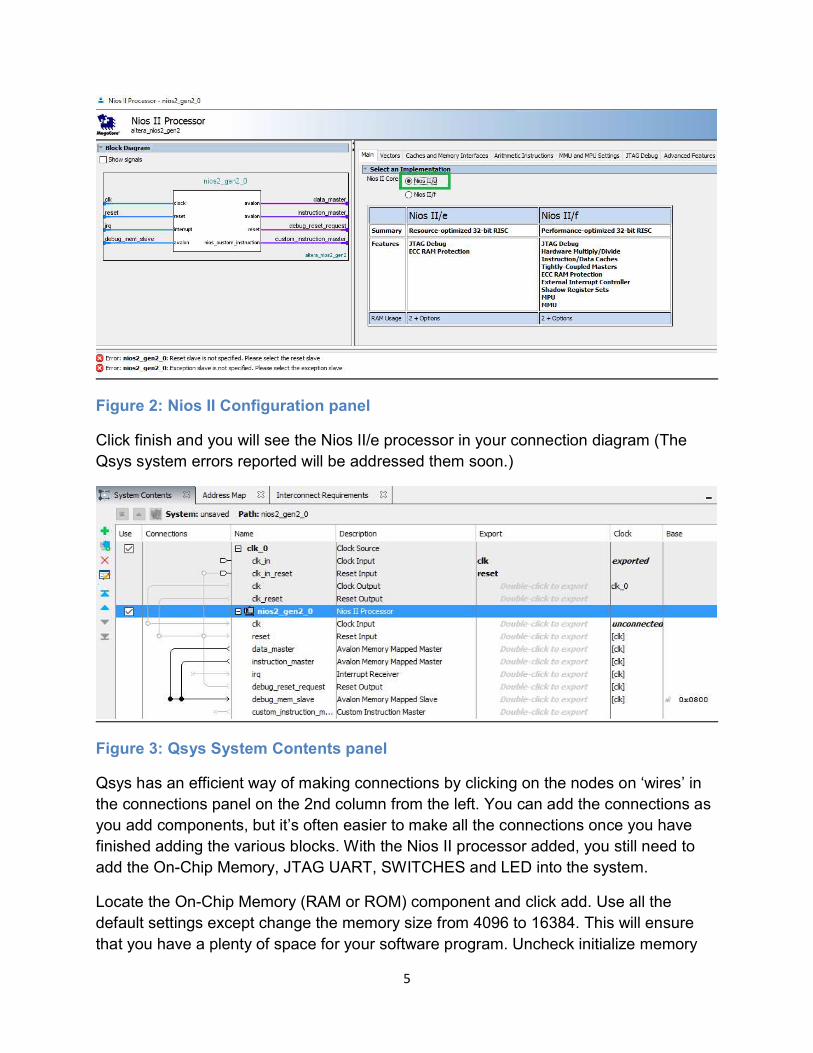
Figure 1: Qsys main panel Next, add the required components of the system and make the connections between them. By default, Qsys inserts a clock module. We will connect to this later on in the lab. Below the IP catalog tab, you can search for the various components you want to add to your Qsys based system. Enter Nios in the search tab and select the Nios II processor from the library. A configuration window will appear, in this select the Nios II/e processor. This version of the Nios II processor is resource optimized and will work well for the Hello World Lab implementation.
5
Figure 2: Nios II Configuration panel
Click finish and you will see the Nios II/e processor in your connection diagram (The Qsys system errors reported will be addressed them soon.)
Figure 3: Qsys System Contents panel
Qsys has an efficient way of making connections by clicking on the nodes on ‘wires’ in the connections panel on the 2nd column from the left. You can add the connections as you add components, but it’s often easier to make all the connections once you have finished adding the various blocks. With the Nios II processor added, you still need to add the On-Chip Memory, JTAG UART, SWITCHES and LED into the system.
Locate the On-Chip Memory (RAM or ROM) component and click add. Use all the default settings except change the memory size from 4096 to 16384. This will ensure that you have a plenty of space for your software program. Uncheck initialize memory

6
content. This feature includes the software executable in the hardware image. For this lab, you will initialize the software executable from Eclipse.
Figure 4: On-chip Memory configuration panel
Click finish and you will now see a total 3 components in your Qsys system: clock, Nios II processor and on-chip memory.
Figure 5: System contents with NIOSII and On-chip Memory
7
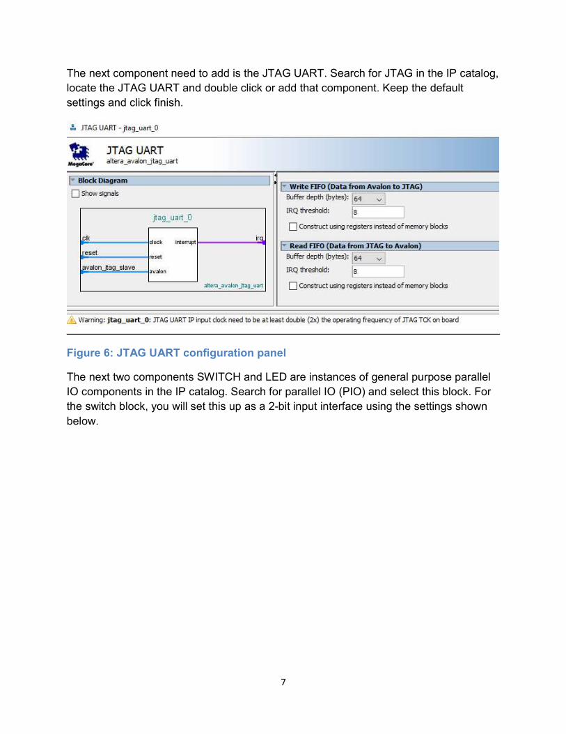
The next component need to add is the JTAG UART. Search for JTAG in the IP catalog, locate the JTAG UART and double click or add that component. Keep the default settings and click finish.
Figure 6: JTAG UART configuration panel
The next two components SWITCH and LED are instances of general purpose parallel IO components in the IP catalog. Search for parallel IO (PIO) and select this block. For the switch block, you will set this up as a 2-bit input interface using the settings shown below.

8
Figure 7: Parallel IO configuration panel for Push Button input
Next, add a second PIO block. Double click on the PIO component as you did for the SWITCH. This time you will configure this component as the LED which is a 2 bit output.
Figure 8: Parallel IO configuration panel for LED outputs
9
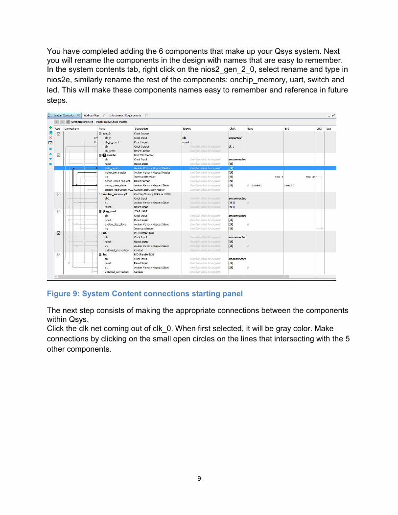
You have completed adding the 6 components that make up your Qsys system. Next you will rename the components in the design with names that are easy to remember. In the system contents tab, right click on the nios2_gen_2_0, select rename and type in nios2e, similarly rename the rest of the components: onchip_memory, uart, switch and led. This will make these components names easy to remember and reference in future steps.
Figure 9: System Content connections starting panel
The next step consists of making the appropriate connections between the components within Qsys. Click the clk net coming out of clk_0. When first selected, it will be gray color. Make connections by clicking on the small open circles on the lines that intersecting with the 5 other components.

10
Figure 10: System contents after clock connection
Perform the same operation to connect the clk_reset to the resets on the other components.
Next, connect the nios2e data master to the slaves. Make the connections between the Nios2e data master and the s1 connection of the onchip memory, avalon_jtag_slave on the uart, s1 port on the switch and s1 port of the led component as shown below.
The instruction master signal from the nios2e component does not need to be connected to each slave component as it only needs access to memory that contains the software executable. Make the connection between the nios2e instruction master and the onchip_memory s1.
The next connections to make are the processor interrupt request (IRQ) signals. The UART can drive interrupts and hence needs to be wired to the nios2e processor interrupt lines. Use the default setting for the IRQ number.
You have now completed the internal connections for this Nios II processor based system. The next step is to make the external connections that connect the Qsys based system to the next higher level in the hierarchy of your FPGA design, or to FPGA device pins that connect to the PCB. Double click on the switch and led conduit items under the export column circled in Figure 28. This will bring these ports out of the Qsys component to connect to the top level design.
11
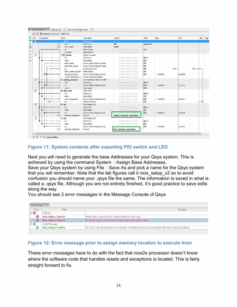
Figure 11: System contents after exporting PIO switch and LED
Next you will need to generate the base Addresses for your Qsys system. This is achieved by using the command System Assign Base Addresses. Save your Qsys system by using File Save As and pick a name for the Qsys system that you will remember. Note that the lab figures call it nios_setup_v2 so to avoid confusion you should name your .qsys file the same. The information is saved in what is called a .qsys file. Although you are not entirely finished, it’s good practice to save edits along the way. You should see 2 error messages in the Message Console of Qsys.
Figure 12: Error message prior to assign memory location to execute from
These error messages have to do with the fact that nios2e processor doesn’t know where the software code that handles resets and exceptions is located. This is fairly straight forward to fix.
12
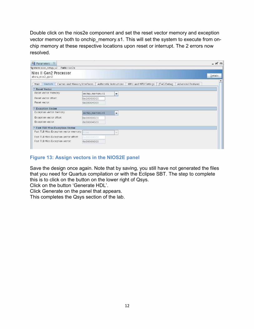
Double click on the nios2e component and set the reset vector memory and exception vector memory both to onchip_memory.s1. This will set the system to execute from on-chip memory at these respective locations upon reset or interrupt. The 2 errors now resolved.
Figure 13: Assign vectors in the NIOS2E panel
Save the design once again. Note that by saving, you still have not generated the files that you need for Quartus compilation or with the Eclipse SBT. The step to complete this is to click on the button on the lower right of Qsys. Click on the button ‘Generate HDL’. Click Generate on the panel that appears. This completes the Qsys section of the lab.
13
Building the top level design
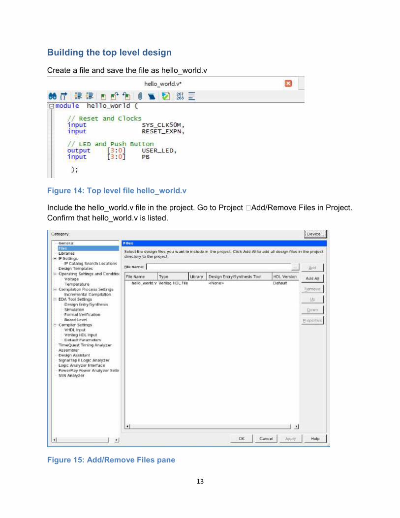
Create a file and save the file as hello_world.v
Figure 14: Top level file hello_world.v
Include the hello_world.v file in the project. Go to Project Add/Remove Files in Project. Confirm that hello_world.v is listed.
Figure 15: Add/Remove Files pane

14
Next, click on General, select the hello_world.v and set as top level entity.
Figure 16: Settings pane
Launch Assignments Pin Planner. Assign the pin locations, IO standard and current strength settings, as below:
Figure 17: Pin Planner
15
Add the Nios II system into design
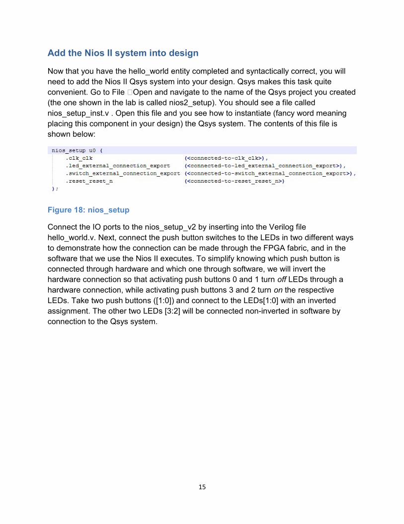
Now that you have the hello_world entity completed and syntactically correct, you will need to add the Nios II Qsys system into your design. Qsys makes this task quite convenient. Go to File Open and navigate to the name of the Qsys project you created (the one shown in the lab is called nios2_setup). You should see a file called nios_setup_inst.v . Open this file and you see how to instantiate (fancy word meaning placing this component in your design) the Qsys system. The contents of this file is shown below:
Figure 18: nios_setup
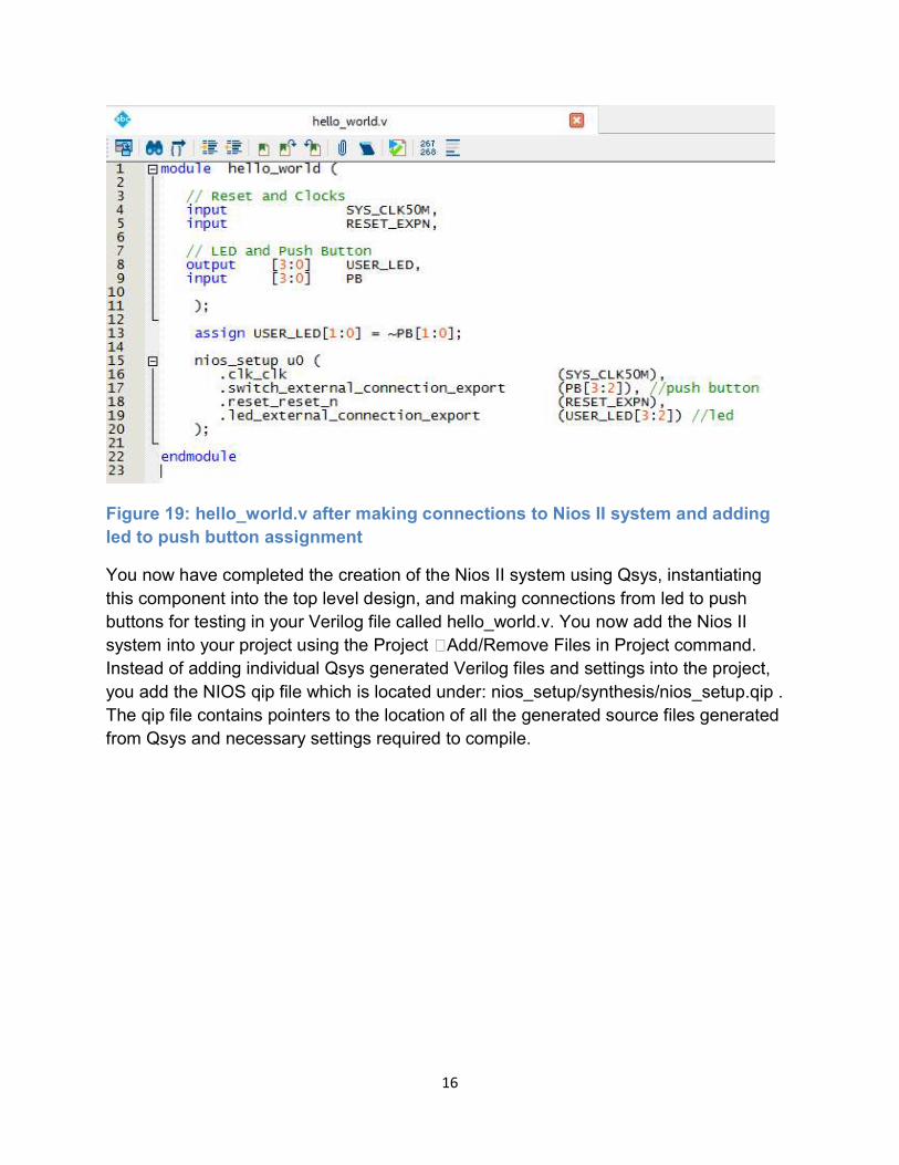
Connect the IO ports to the nios_setup_v2 by inserting into the Verilog file hello_world.v. Next, connect the push button switches to the LEDs in two different ways to demonstrate how the connection can be made through the FPGA fabric, and in the software that we use the Nios II executes. To simplify knowing which push button is connected through hardware and which one through software, we will invert the hardware connection so that activating push buttons 0 and 1 turn off LEDs through a hardware connection, while activating push buttons 3 and 2 turn on the respective LEDs. Take two push buttons ([1:0]) and connect to the LEDs[1:0] with an inverted assignment. The other two LEDs [3:2] will be connected non-inverted in software by connection to the Qsys system.
16
Figure 19: hello_world.v after making connections to Nios II system and adding led to push button assignment
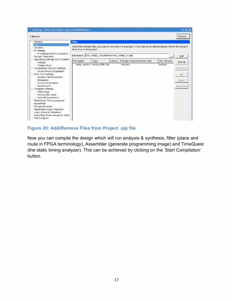
You now have completed the creation of the Nios II system using Qsys, instantiating this component into the top level design, and making connections from led to push buttons for testing in your Verilog file called hello_world.v. You now add the Nios II system into your project using the Project Add/Remove Files in Project command. Instead of adding individual Qsys generated Verilog files and settings into the project, you add the NIOS qip file which is located under: nios_setup/synthesis/nios_setup.qip . The qip file contains pointers to the location of all the generated source files generated from Qsys and necessary settings required to compile.
17
Figure 20: Add/Remove Files from Project .qip file
Now you can compile the design which will run analysis & synthesis, fitter (place and route in FPGA terminology), Assembler (generate programming image) and TimeQuest (the static timing analyzer). This can be achieved by clicking on the ‘Start Compilation’ button.
18
SOFTWARE DESIGN
Creating the Software for the “Hello World” design
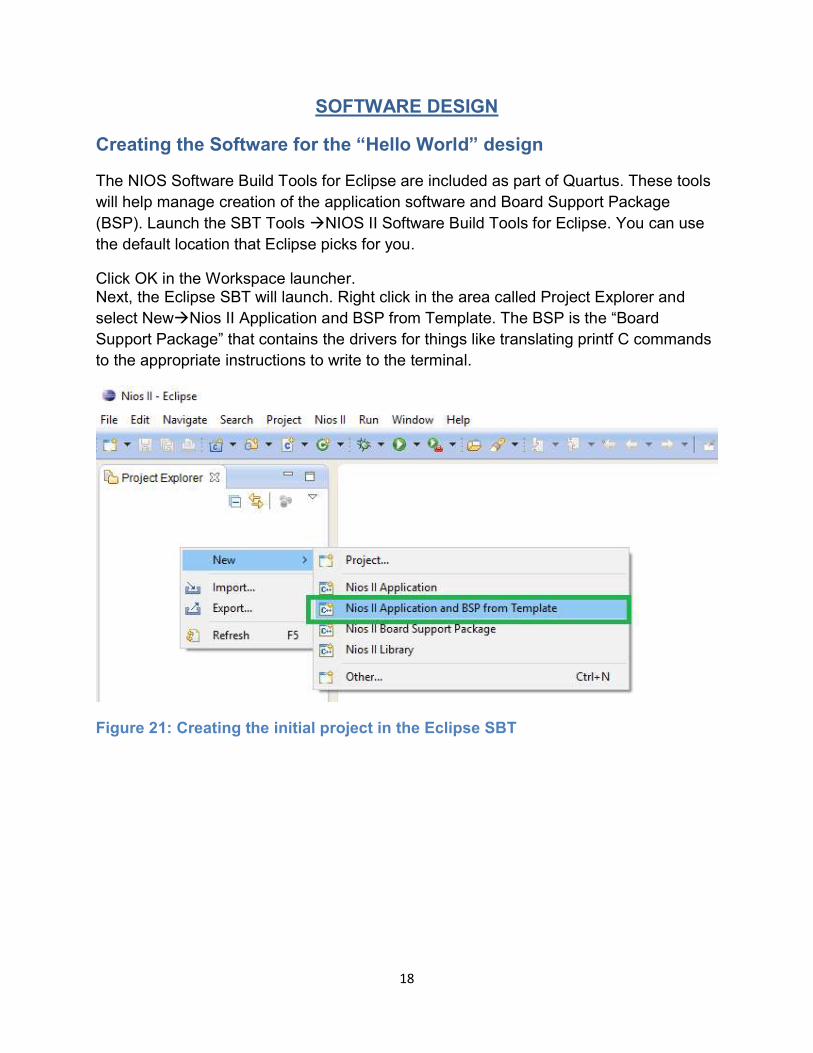
The NIOS Software Build Tools for Eclipse are included as part of Quartus. These tools will help manage creation of the application software and Board Support Package (BSP). Launch the SBT Tools NIOS II Software Build Tools for Eclipse. You can use the default location that Eclipse picks for you.
Click OK in the Workspace launcher. Next, the Eclipse SBT will launch. Right click in the area called Project Explorer and select NewNios II Application and BSP from Template. The BSP is the “Board Support Package” that contains the drivers for things like translating printf C commands to the appropriate instructions to write to the terminal.
Figure 21: Creating the initial project in the Eclipse SBT

19
Next you will see a panel that requests information to setup your design. First, you need to navigate to your working directory and click on the .sopcinfo file. The .sopcinfo file trains Eclipse on what your Qsys system contains. Click OK.
Figure 22: Navigating to correct .sopcinfo file

20
Fill in the Project name. Call it hello_world. Next you will be asked to pick a template design. The Hello World Small is a software application to write “Hello from Nios II” to the screen. Click Finish. Note: make sure to pick Hello World Small and not Hello World or you will not have enough memory in your FPGA design to store the program executable.
Figure 23: completing the Nios II Software Examples setup screen with project name and project template.

21
Now, make some modifications to the code to connect the LEDs to the push button switches through software. Click the right arrow next to hello_world. It will show the contents of your project. Double-click hello_world_small.c . Note the command alt_putstr to write text to the terminal. This is part of the Altera HAL (Hardware Abstraction Layer) set of software functions. A complete list of these functions can be found in the Nios II Software Developer’s Handbook https://www.altera.com/en_US/pdfs/literature/hb/nios2/n2sw_nii5v2.pdf
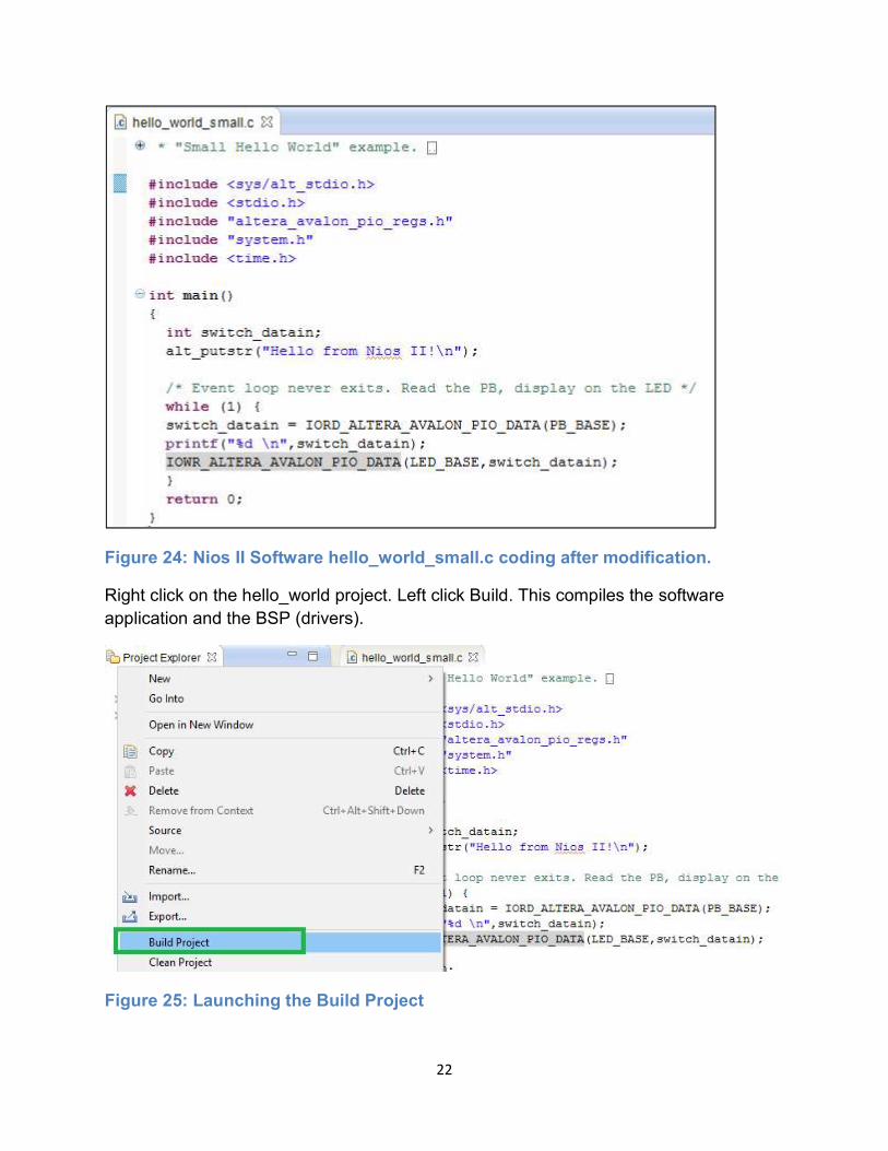
Add a library declaration, define integer switch_datain, and a few HAL functions to connect the LEDs to the Push Buttons:
#include <sys/alt_stdio.h> #include <stdio.h> #include "altera_avalon_pio_regs.h" #include "system.h" #include <time.h> int main() { int switch_datain; alt_putstr("Hello from Nios II!\n"); /* Event loop never exits. Read the PB, display on the LED */ while (1) { switch_datain = IORD_ALTERA_AVALON_PIO_DATA(PB_BASE); printf("%d \n",switch_datain); IOWR_ALTERA_AVALON_PIO_DATA(LED_BASE,switch_datain); } return 0; }
22
Figure 24: Nios II Software hello_world_small.c coding after modification.
Right click on the hello_world project. Left click Build. This compiles the software application and the BSP (drivers).
Figure 25: Launching the Build Project

23
Downloading the hardware into Cyclone 10 LP Development Kit
To work with the Cyclone 10 LP development kit in the context of this lab, you just need to connect the USB blaster from PC to the dev kit. The development kit will be power-up by the USB Blaster cable itself from PC (no extra power supply needed).
Figure 26: Cyclone 10 LP Development Kit connect to USB Blaster cable from PC. In Quartus, launch the Tools Programmer. Click Auto Detect and make sure the USB Blaster is detected before download the “.sof” file or SRAM object file. This is the programming image file that gets downloaded in the FPGA. The default location is <working_directory>/output_files. Click Start. When programming is complete, the Progress meter should read 100% (Successful).

24
Run the Nios II Software Download the .elf (software executable) into the Nios IIe processor. Return to the Eclipse SBT tools. Right click on hello_world_sw and select Run as Run Nios II Hardware. Click on the Target Connection tab. The connection should indicate that Eclipse has connected to USB-blaster.
Figure 27: Run (Nios II) Configurations Window in Eclipse. Now you have hardware and software downloaded into the Cyclone 10 LP Development Kit. You should observe “Hello from Nios II” in the Nios II Console tab. You can also test the connections between push button and LEDs. Recall that 2 buttons [1:0] are connected in hardware are inverted so by default the LEDs are on. Buttons [3:2] are connected in the C code and illuminate LEDs [3:2] when pushed. Press the push buttons to operate the LEDs based on the hello_world.v and hello_world_small.c source files. Be careful not to hit the push buttons CONFIG or RESET or you can disrupt the FPGA programmed status. (Note: By default, Nios II Console tab will continuously print out the value of USER_LED[3:2]=0x3 ). Press PB0: USER_LED[0] will Off Press PB1: USER_LED[1] will Off Press PB2: USER_LED[3:2] value is 0x2 Press PB3: USER_LED[3:2] value is 0x1 Press both PB2 and PB3 simultaneously: USER_LED[3:2] value is 0x0
25
Summary The hardware and software sections of this lab includes: 1. Using Qsys to build a Nios II based system 2. Instantiating the Qsys component into your top level design 3. Add some connections between push buttons and LEDs 4. Compiling your hardware 5. Importing the Nios II based system into the Eclipse Software Build Tools 6. Building a software project 7. Modifying a software template to perform some simple IO functions 8. Downloading the hardware image into the Cyclone 10 LP Development Kit 9. Downloading the software executable into the Cyclone 10 LP Development Kit 10. Testing the hardware

26
Revision and History
Date Version Changes 8/25/2017 1.0 Initial Release