by himanshu devices and peripheral microprocessor · 8255 ppi, 8253 pit,8279 and 8257 dma...
TRANSCRIPT
MICROPROCESSOR AND PERIPHERAL
DEVICESBy Himanshu
Detailed Contents :-1.Evolution of Microprocessor Typical organization of a microcomputer system and functions of its various blocks.
Microprocessor, its evolution, function and impact on modern society.2.Architecture of a Microprocessor (With reference to 8085 microprocessor)
Concept of Bus, bus organization of 8085, Functional block diagram of 8085 and function of each block, Pin details of 8085 and related signals, Demultiplexing of address/data bus generation of read/write control signals, Steps to execute a stored programme.
3.Instruction Timing and Cycles Instruction cycle, machine cycle and T-states, Fetch and execute cycle.
4.Programming (with respect to 8085 microprocessor) Brief idea of machine and assembly languages, Machines and Mnemonic codes. Instruction format and Addressing mode.
Identification of instructions as to which addressing mode they belong. Concept of Instruction set. Explanation of the instructions of the following groups of instruction set. Data transfer group, Arithmetic Group, Logic Group, Stack, I/O and Machine Control Group. Programming exercises in assembly language. (Examples can be taken from the list of experiments).
5.Memories and I/O interfacing Concept of memory mapping, partitioning of total memory space. Address decoding,
concept of peripheral mapped I/O and memory mapped I/O. Interfacing of memory mapped I/O devices.
6.Interrupts Concept of interrupt, Maskable and non-maskable, Edge triggered and level triggered
interrupts, Software interrupt, Restart interrupts and its use, Various hardware interrupts of 8085, Servicing interrupts, extending interrupt system.
7.Data Transfer Techniques Concept of programmed I/O operations, sync data transfer, async data transfer (hand
shaking), Interrupt driven data transfer, DMA, Serial output data, Serial input data.8.Peripheral devices 8255 PPI, 8253 PIT,8279 and 8257 DMA controller.
Microprocessor 8085 :-⚫ 1st Generation: This was the period during 1971 to 1973 of microprocessor’s
history. In 1971, INTEL created the first microprocessor 4004 that would run at a clock speed of 108 KHz. During this period, the other microprocessors in the market including Rockwell international PPS-4, INTEL-8008 and National semiconductors IMP-16 were in use. But, all these were not TTL compatible processors.
⚫ 2nd Generation: This was the period during 1973 to 1978 in which very efficient 8-bit microprocessors were implemented like Motorola 6800 and 6801, INTEL-8085 and Zilogs-Z80, which were among the most popular ones. Owing to their superfast speed, they were costly as they were based on NMOS fabrication technology.
⚫ 3rd Generation: During this period 16 bit processors were created and designed using HMOS technology. From 1979 to 1980, INTEL 8086/80186/80286 and Motorola 68000 and 68010 were developed. Speeds of those processors were four times better than the 2nd generation processors.
⚫ 4th Generation: From 1981 to 1995 this generation developed 32 bit microprocessors by using HCMOS fabrication. INTEL-80386 and Motorola’s 68020/68030 were the popular processors.
⚫ 5th Generation: From 1995 to until now this generation has been bringing out high-performance and high-speed processors that make use of 64-bit processors. Such processors include Pentium, Celeron, Dual and Quad core processors.
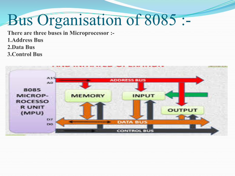
Bus Organisation of 8085 :-There are three buses in Microprocessor :-1.Address Bus2.Data Bus3.Control Bus
1. Address Bus:- Microprocessor has 16 bit address bus. The bus over which the CPU sends out the address of the memory location is known as Address bus. The address bus carries the address of memory location to be written or to be read from.The address bus is unidirectional. It means bits flowing occurs only in one direction, only from microprocessor to peripheral devices.We can find that how much memory location it can using the formula 2^N. where N is the number of bits used for address lines.here, 2^16 = 65536bytes or 64KbSo we can say that it can access upto 64 kb memory location.
2. Data Bus:-8085 Microprocessor has 8 bit data bus. So it can be used to carry the 8 bit data starting from 00000000H(00H) to 11111111H(FFH). Here 'H' tells the Hexadecimal Number. It is bidirectional. These lines are used for data flowing in both direction means data can be transferred or can be received through these lines. The data bus also connects the I/O ports and CPU. The largest number that can appear on the data bus is 11111111.
It has 8 parallel lines of data bus. So it can access upto 2^8 = 256 data bus lines.3. Control Bus:-The control bus is used for sending control signals to the memory and I/O devices. The CPU sends control signal on the control bus to enable the outputs of addressed memory devices or I/O port devices.
Some of the control bus signals are as follows:1. Memory read2. Memory write3. I/O read4. I/O write.
Microprocessor 8085 :-⚫ 8085 is pronounced as "eighty-eighty-five" microprocessor. It is an 8-bit
microprocessor designed by Intel in 1977 using NMOS technology.⚫ It has the following configuration −⚫ 8-bit data bus⚫ 16-bit address bus, which can address upto 64KB⚫ A 16-bit program counter⚫ A 16-bit stack pointer⚫ Six 8-bit registers arranged in pairs: BC, DE, HL⚫ Requires +5V supply to operate at 3.2 MHZ single phase clock⚫ It is used in washing machines, microwave ovens, mobile phones, etc.
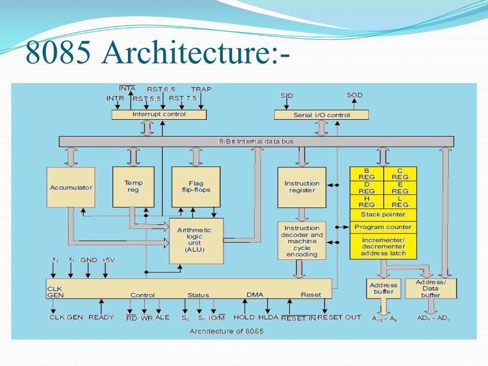
8085 Architecture:-
8085 Microprocessor – Functional Units :-8085 consists of the following functional units −▪AccumulatorIt is an 8-bit register used to perform arithmetic, logical, I/O & LOAD/STORE operations. It is connected to internal data bus & ALU.▪Arithmetic and logic unitAs the name suggests, it performs arithmetic and logical operations like Addition, Subtraction, AND, OR, etc. on 8-bit data.▪General purpose registerThere are 6 general purpose registers in 8085 processor, i.e. B, C, D, E, H & L. Each register can hold 8-bit data.These registers can work in pair to hold 16-bit data and their pairing combination is like B-C, D-E & H-L.▪Program counterIt is a 16-bit register used to store the memory address location of the next instruction to be executed. Microprocessor increments the program whenever an instruction is being executed, so that the program counter points to the memory address of the next instruction that is going to be executed.
▪Stack pointerIt is also a 16-bit register works like stack, which is always incremented/decremented by 2 during push & pop operations.▪Temporary registerIt is an 8-bit register, which holds the temporary data of arithmetic and logical operations.▪Flag registerIt is an 8-bit register having five 1-bit flip-flops, which holds either 0 or 1 depending upon the result stored in the accumulator.These are the set of 5 flip-flops −Sign (S)Zero (Z)Auxiliary Carry (AC)Parity (P)Carry (C)Its bit position is shown in the following table −
D7 D6 D5 D4 D3 D2 D1 D0S Z AC P CY
▪Instruction register and decoderIt is an 8-bit register. When an instruction is fetched from memory then it is stored in the Instruction register. Instruction decoder decodes the information present in the Instruction register.▪Timing and control unitIt provides timing and control signal to the microprocessor to perform operations. Following are the timing and control signals, which control external and internal circuits −Control Signals: READY, RD’, WR’, ALEStatus Signals: S0, S1, IO/M’DMA Signals: HOLD, HLDARESET Signals: RESET IN, RESET OUT▪Interrupt controlAs the name suggests it controls the interrupts during a process. When a microprocessor is executing a main program and whenever an interrupt occurs, the microprocessor shifts the control from the main program to process the incoming request. After the request is completed, the control goes back to the main program.
There are 5 interrupt signals in 8085 microprocessor: INTR, RST 7.5, RST 6.5, RST 5.5, TRAP.▪Serial Input/output controlIt controls the serial data communication by using these two instructions: SID (Serial input data) and SOD (Serial output data).▪Address buffer and address-data bufferThe content stored in the stack pointer and program counter is loaded into the address buffer and address-data buffer to communicate with the CPU. The memory and I/O chips are connected to these buses; the CPU can exchange the desired data with the memory and I/O chips.Address bus and data busData bus carries the data to be stored. It is bidirectional, whereas address bus carries the location to where it should be stored and it is unidirectional. It is used to transfer the data & Address I/O devices.
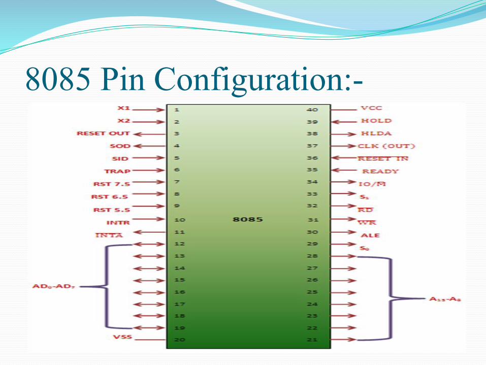
8085 Pin Configuration:-
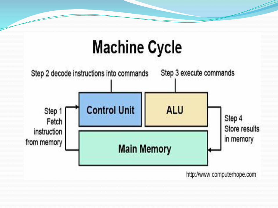
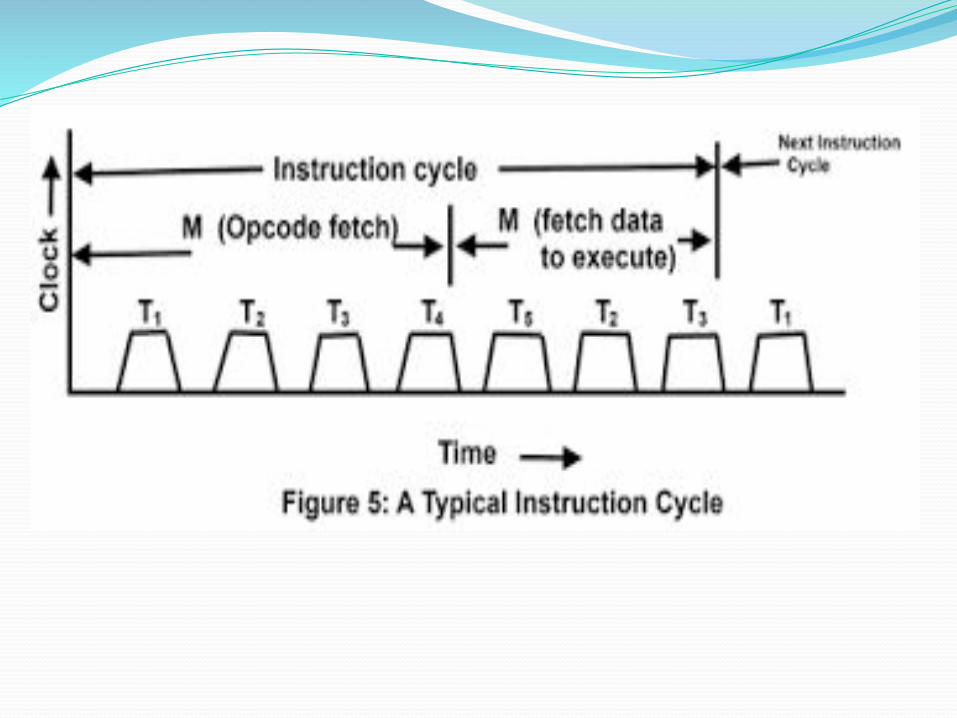
Different Cycles of 8085 :- Instruction Cycle :- The Steps required by CPU to fetch and execute an
Instruction is called a Instruction Cycle. It consist of fetch and Execute Cycle. Instruction Cycle=Fetch Cycle + Execute Cycle
Machine Cycle :- It is a time Required by microprocessor to complete the operation of accessing memory or I/O devices is called machine cycle. It perform specific operation like opcode fetch, memory read, write, I/O read/write are performed in machine cycle.The machine cycle is a 4 process cycle that includes reading and interpreting the machine language, executing the code and then storing that code.
Four steps of Machine cycle⚫ Fetch - Retrieve an instruction from the memory.⚫ Decode - Translate the retrieved instruction into a series of computer commands.⚫ Execute - Execute the computer commands.⚫ Store - Send and write the results back in memory.
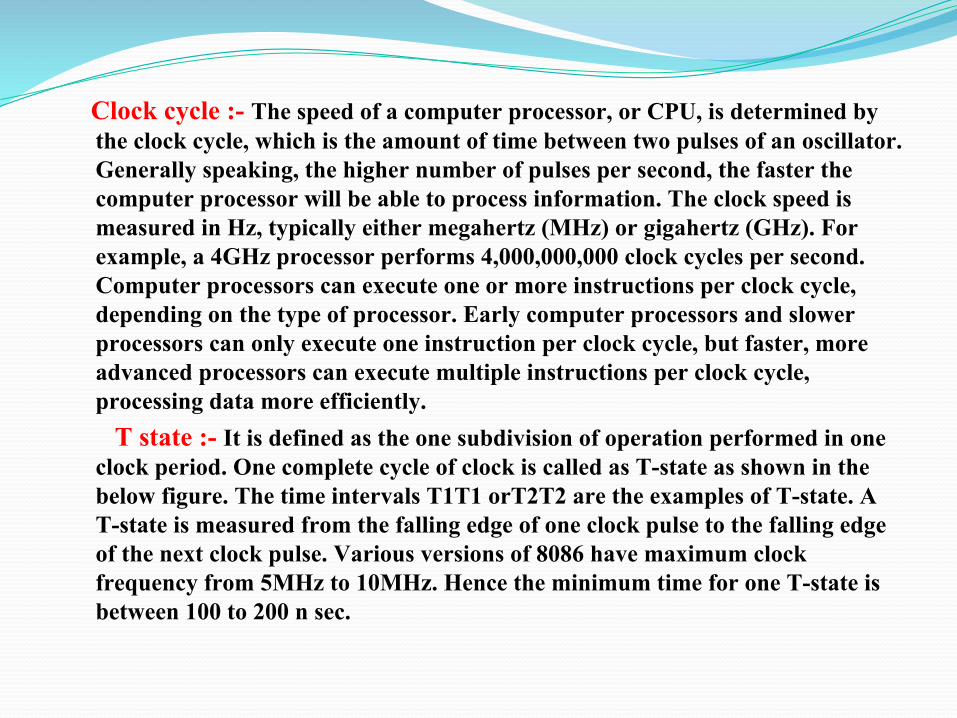
Clock cycle :- The speed of a computer processor, or CPU, is determined by the clock cycle, which is the amount of time between two pulses of an oscillator. Generally speaking, the higher number of pulses per second, the faster the computer processor will be able to process information. The clock speed is measured in Hz, typically either megahertz (MHz) or gigahertz (GHz). For example, a 4GHz processor performs 4,000,000,000 clock cycles per second.Computer processors can execute one or more instructions per clock cycle, depending on the type of processor. Early computer processors and slower processors can only execute one instruction per clock cycle, but faster, more advanced processors can execute multiple instructions per clock cycle, processing data more efficiently.
T state :- It is defined as the one subdivision of operation performed in one clock period. One complete cycle of clock is called as T-state as shown in the below figure. The time intervals T1T1 orT2T2 are the examples of T-state. A T-state is measured from the falling edge of one clock pulse to the falling edge of the next clock pulse. Various versions of 8086 have maximum clock frequency from 5MHz to 10MHz. Hence the minimum time for one T-state is between 100 to 200 n sec.
Brief Idea of Languages :-Machine Language:- The machine language is the internal language of the computer system. It is a difficult programming language to handle by any humans. It is usually made up of a binary string of 0s and 1s that is understood by the machine to follow any instructions. Infact, we can say that the machine can only recognize these 0s and 1s and nothing else. So, it is a language of the lowest degree made for machines only. Programmes therefore prefers to use either a high-level programming language or an assembly language to deliver various instructions by translating it to machine understandable codes known as machine codes.
Assembly Language:- Assembly language is a second generation programming language used in the computer systems. In assembly language, a programmer uses symbolic instructions instead of machine language instructions and descriptive names for data items and memory location.
An assembly language program is written according to strict rules and then translated by an assembler into machine code. It is machine dependant language hence it is not portable. It has very less restrictions and also features high interaction between the operating system and the hardware thus enabling to write easy hardware dependant programs. The various symbolic notations used in the assembly language is called mnemonics.High Level Language :- Sometimes abbreviated as HLL, a high-level language is a
computer programming language that isn't limited by the computer, designed for a specific job, and is easier to understand. It is more like human language and less like machine language. However, for a computer to understand and run a program created with a high-level language, it must be compiled into machine language.
The first high-level languages were introduced in the 1950's. Today, high-level languages are in widespread use. These include BASIC, C, C++, Cobol, FORTRAN, Java, Pascal, Perl, PHP and Visual Basic.
Addressing Modes of 8085:-(i)Immediate Addressing mode :- In this mode operand is a part of the
instruction itself is known as Immediate Addressing mode. If the immediate data is 8-bit, the instruction will be of two bytes. If the immediate data is 16 bit, the instruction is of 3 bytes.
⚫ Ex: (1). ADI DATA ; Add immediate the data to the contents of the accumulator.(2).LXIH 8500H : Load immediate the H-L pair with the operand 8500H(3). MVI 08H ; Move the data 08 H immediately to the accumulator(4). SUI 05H ; Subtract immediately the data 05H from the accumulator
(ii) Direct Addressing mode:- The mode of addressing in which the 16-bit address of the operand is directly available in the instruction itself is called Direct Addressing mode. i.e., the address of the operand is available in the instruction itself. This is a 3-byte instruction.
⚫ Ex: (1). LDA 9525H; Load the contents of memory location into Accumulator.⚫ (2). STA 8000H; Store the contents of the Accumulator in the location 8000H⚫ (3). IN 01H; Read the data from port whose address is 01H.
(iii). Register addressing modes:- In this mode the operands are microprocessor registers only. i.e. the operation is performed within various registers of the microprocessor.
⚫ Ex: (1). MOV A, B; Move the contents of B register to A register.⚫ (2). SUB D; Subtract the contents of D register from Accumulator.⚫ (3). ADD B, C; Add the contents of C register to the contents of B register.
(iv). Register indirect addressing modes:- The 16-bit address location of the operand stored in a register pair (H-L) is given in the instruction. The address of the operand is given in an indirect way with the help of a register pair. So it is called Register indirect addressing mode.
⚫ Ex: (1). LXIH 9570H : Load immediate the H-L pair with the address of the location 9570H.
⚫ MOV A, M : Move the contents of the memory location pointed by the H-L pair to accumulator.
(v). Implicit Addressing mode:- The mode of instruction which do not specify the operand in the instruction but it is implicated, is known as implicit addressing mode. i.e., the operand is supposed to be present generally in accumulator.Ex: (1).CMA; complement the contents of Accumulator(2).CMC; Complement carry(3). RLC; Rotate Accumulator left by one bit(4). RRC; Rotate Accumulator right by one bit(5). STC; Set carry.
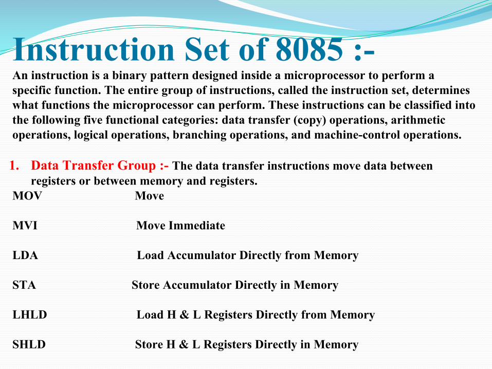
Instruction Set of 8085 :-An instruction is a binary pattern designed inside a microprocessor to perform a specific function. The entire group of instructions, called the instruction set, determines what functions the microprocessor can perform. These instructions can be classified into the following five functional categories: data transfer (copy) operations, arithmetic operations, logical operations, branching operations, and machine-control operations. 1. Data Transfer Group :- The data transfer instructions move data between
registers or between memory and registers.MOV Move MVI Move Immediate LDA Load Accumulator Directly from Memory STA Store Accumulator Directly in Memory LHLD Load H & L Registers Directly from Memory SHLD Store H & L Registers Directly in Memory
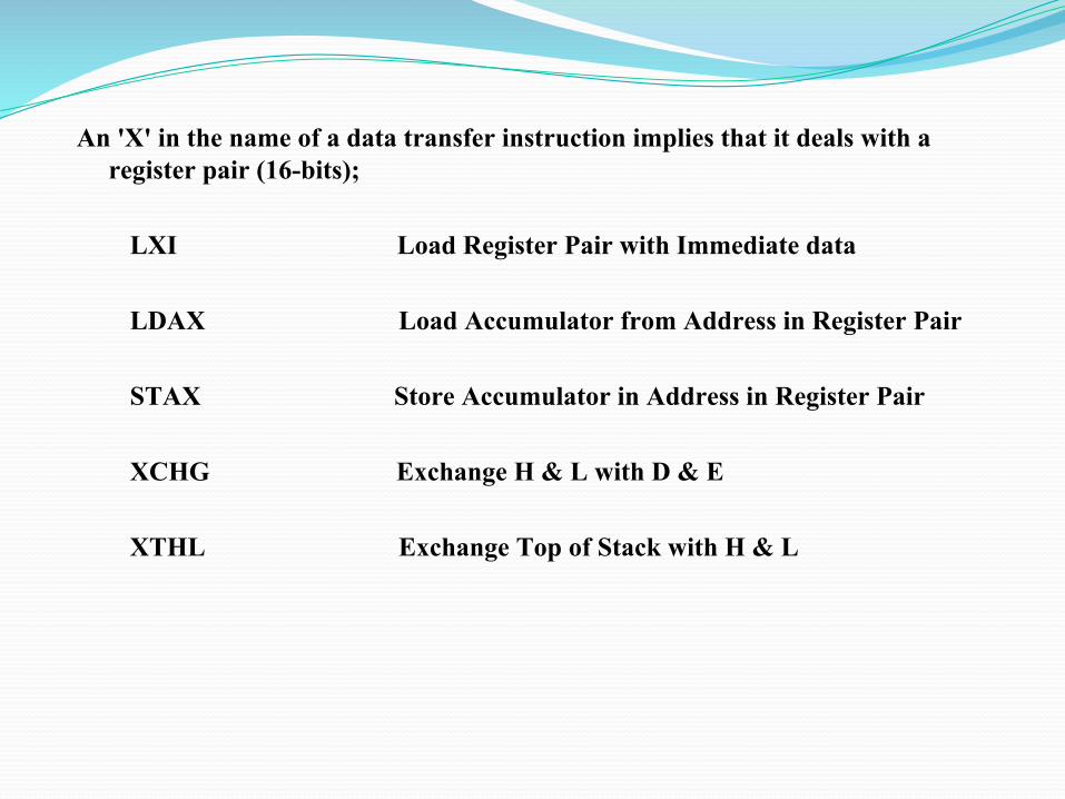
An 'X' in the name of a data transfer instruction implies that it deals with a register pair (16-bits);
LXI Load Register Pair with Immediate data
LDAX Load Accumulator from Address in Register Pair
STAX Store Accumulator in Address in Register Pair
XCHG Exchange H & L with D & E
XTHL Exchange Top of Stack with H & L
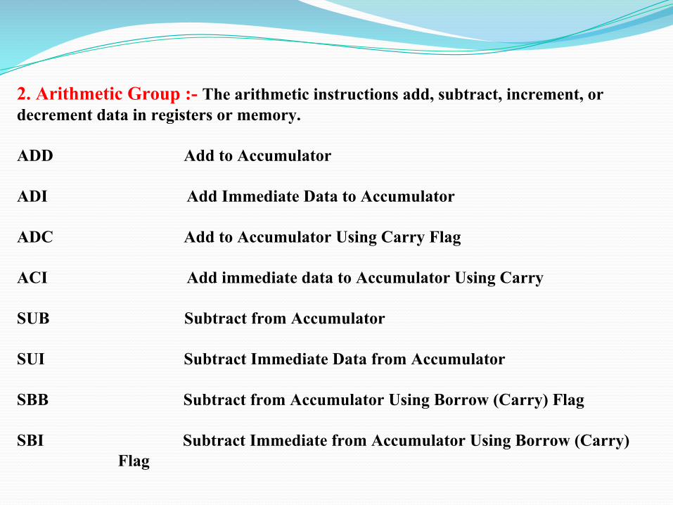
2. Arithmetic Group :- The arithmetic instructions add, subtract, increment, or decrement data in registers or memory. ADD Add to Accumulator ADI Add Immediate Data to Accumulator ADC Add to Accumulator Using Carry Flag ACI Add immediate data to Accumulator Using Carry SUB Subtract from Accumulator SUI Subtract Immediate Data from Accumulator SBB Subtract from Accumulator Using Borrow (Carry) Flag SBI Subtract Immediate from Accumulator Using Borrow (Carry)
Flag
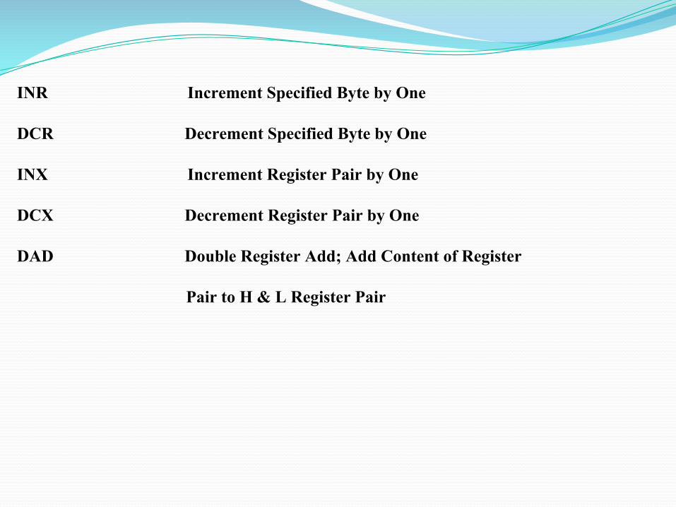
INR Increment Specified Byte by One DCR Decrement Specified Byte by One INX Increment Register Pair by One DCX Decrement Register Pair by One DAD Double Register Add; Add Content of Register Pair to H & L Register Pair
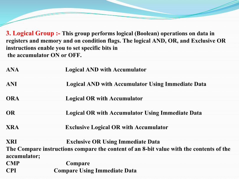
3. Logical Group :- This group performs logical (Boolean) operations on data in registers and memory and on condition flags. The logical AND, OR, and Exclusive OR instructions enable you to set specific bits in the accumulator ON or OFF. ANA Logical AND with Accumulator ANI Logical AND with Accumulator Using Immediate Data ORA Logical OR with Accumulator OR Logical OR with Accumulator Using Immediate Data XRA Exclusive Logical OR with Accumulator XRI Exclusive OR Using Immediate DataThe Compare instructions compare the content of an 8-bit value with the contents of the accumulator;CMP Compare CPI Compare Using Immediate Data
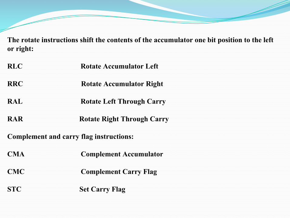
The rotate instructions shift the contents of the accumulator one bit position to the left or right: RLC Rotate Accumulator Left RRC Rotate Accumulator Right RAL Rotate Left Through Carry RAR Rotate Right Through Carry Complement and carry flag instructions: CMA Complement Accumulator CMC Complement Carry Flag STC Set Carry Flag
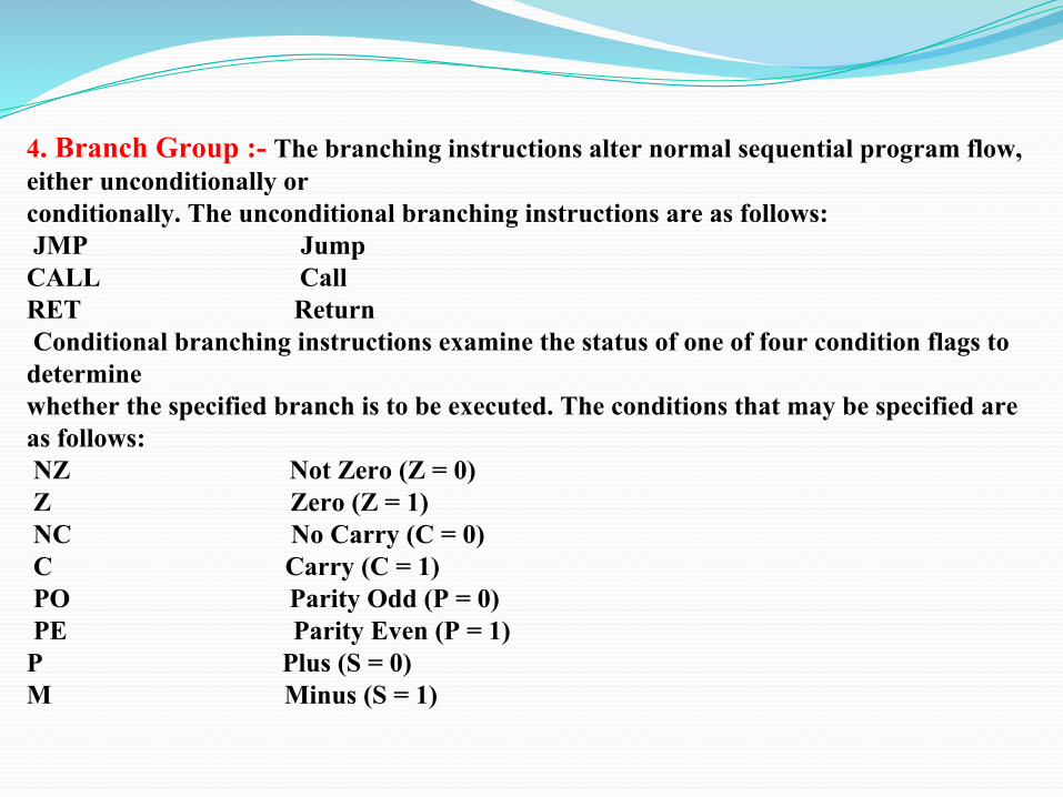
4. Branch Group :- The branching instructions alter normal sequential program flow, either unconditionally orconditionally. The unconditional branching instructions are as follows: JMP JumpCALL CallRET Return Conditional branching instructions examine the status of one of four condition flags to determinewhether the specified branch is to be executed. The conditions that may be specified are as follows: NZ Not Zero (Z = 0) Z Zero (Z = 1) NC No Carry (C = 0) C Carry (C = 1) PO Parity Odd (P = 0) PE Parity Even (P = 1)P Plus (S = 0)M Minus (S = 1)
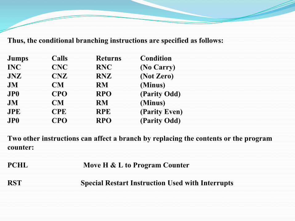
Thus, the conditional branching instructions are specified as follows: Jumps Calls Returns Condition INC CNC RNC (No Carry)JNZ CNZ RNZ (Not Zero)JM CM RM (Minus)JP0 CPO RPO (Parity Odd)JM CM RM (Minus)JPE CPE RPE (Parity Even)JP0 CPO RPO (Parity Odd) Two other instructions can affect a branch by replacing the contents or the program counter: PCHL Move H & L to Program Counter RST Special Restart Instruction Used with Interrupts
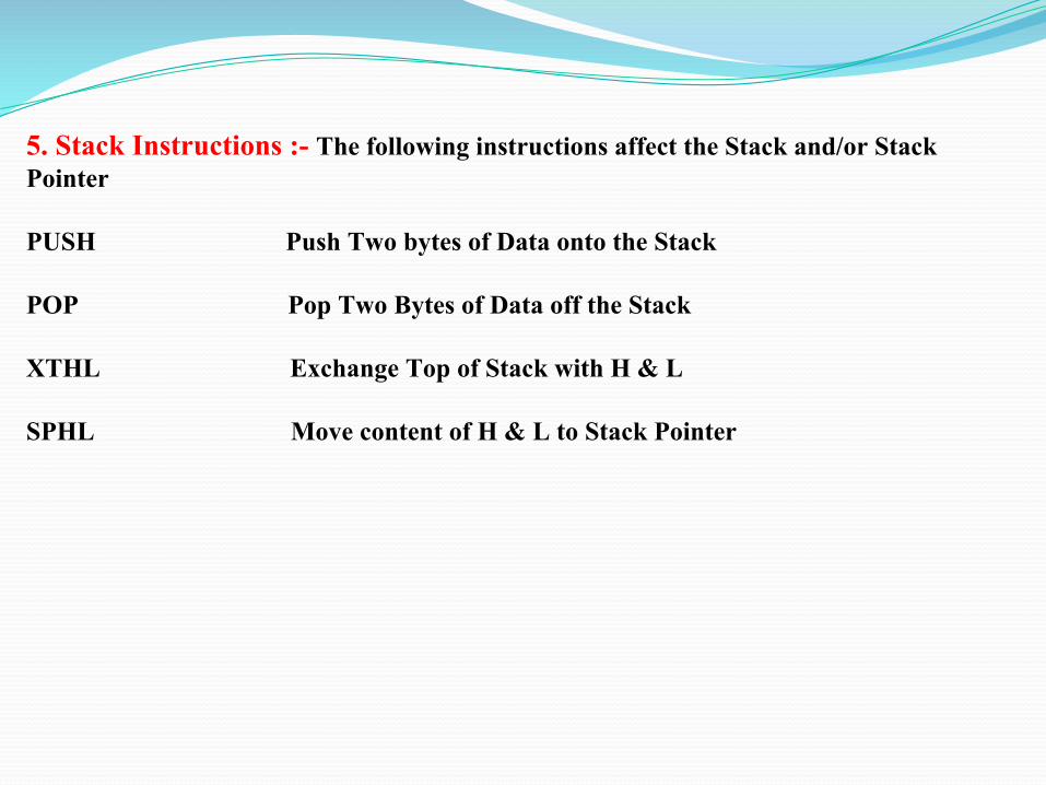
5. Stack Instructions :- The following instructions affect the Stack and/or Stack Pointer PUSH Push Two bytes of Data onto the Stack POP Pop Two Bytes of Data off the Stack XTHL Exchange Top of Stack with H & L SPHL Move content of H & L to Stack Pointer
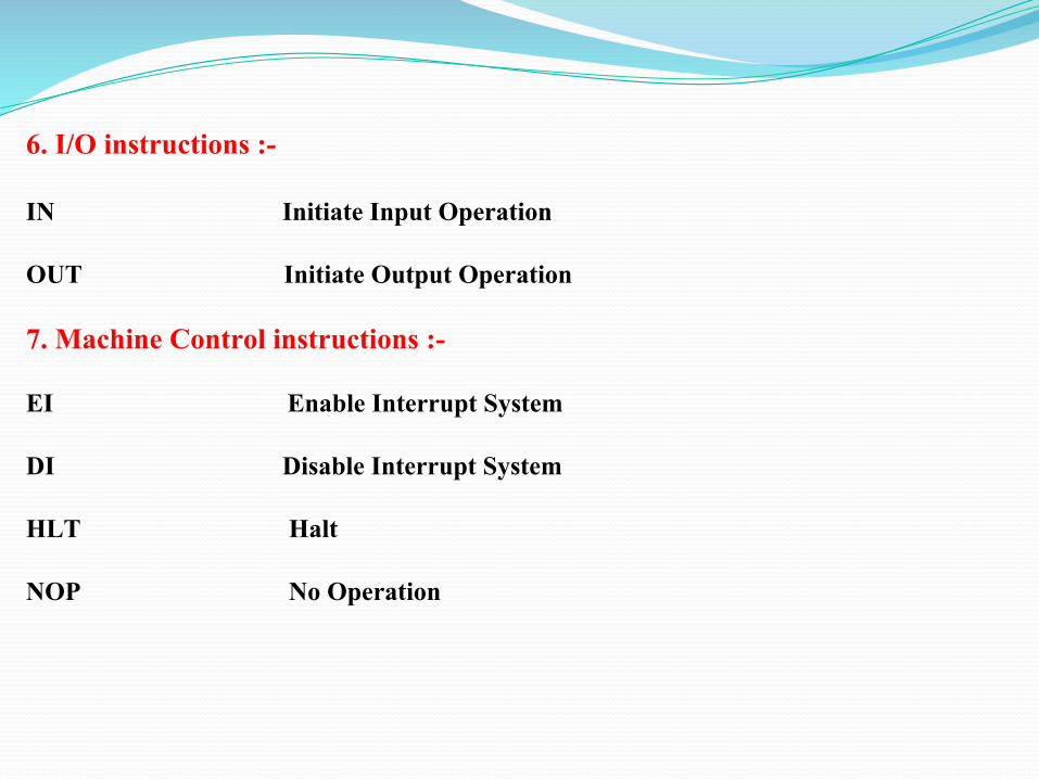
6. I/O instructions :- IN Initiate Input Operation OUT Initiate Output Operation
7. Machine Control instructions :- EI Enable Interrupt System DI Disable Interrupt System HLT Halt NOP No Operation

THANK YOU