bulk and surface passivation of silicon solar cells ... and surface passivation of silicon solar...
TRANSCRIPT
PROGRESS IN PHOTOVOLTAICS: RESEARCH AND APPLICATIONS
Prog. Photovolt: Res. Appl. 2005; 13:551–569
Published online 25 April 2005 in Wiley InterScience (www.interscience.wiley.com). DOI: 10.1002/pip.611
Bulk and Surface Passivationof Silicon Solar CellsAccomplished by Silicon NitrideDeposited on Industrial Scaleby Microwave PECVDWim Soppe*,y, Henk Rieffe and Arthur WeeberEnergy Research Centre of the Netherlands, ECN, P.O. Box 1, 1755 ZG Petten, The Netherlands
Bulk and surface passivation by silicon nitride has become an indispensable element
in industrial production of multicrystalline silicon (mc-Si) solar cells. Microwave
PECVD is a very effective method for high-throughput deposition of silicon nitride
layers with the required properties for bulk and surface passivation. In this paper an
analysis is presented of the relation between deposition parameters of microwave
PECVD and material properties of silicon nitride. By tuning the process conditions
(substrate temperature, gas flows, working pressure) we have been able to fabricate
silicon nitride layers which fulfill almost ideally the four major requirements for mc-
Si solar cells: (1) good anti-reflection coating (refractive index tunable between 2�0and 2�3); (2) good surface passivation on p-type FZ wafers (Seff< 30 cm/s); (3) good
bulk passivation (improvement of IQE at 1000 nm by 30% after short thermal
anneal); (4) long-term stability (no observable degradation after several years of
exposure to sunlight). By implementing this silicon nitride deposition in an inline
production process of mc-Si solar cells we have been able to produce cells with an
efficiency of 16�5%.
Finally, we established that the continuous deposition process could be maintained
for at least 20 h without interruption for maintenance. On this timescale we did not
observe any significant changes in layer properties or cell properties. This shows the
robustness of microwave PECVD for industrial production. Copyright # 2005 John
Wiley & Sons, Ltd.
key words: silicon nitride; microwave PECVD; surface passivation; bulk passivation; multi-
crystalline slicon; solar cells; internal quantum efficiency
Received 25 August 2004
Copyright # 2005 John Wiley & Sons, Ltd. Revised 24 November 2004
*Correspondence to: Wim Soppe, Energy Research Centre of the Netherlands (ECN), PO Box 1, 1755 ZG Petten, The Netherlands.yE-mail: [email protected]
Contract/grant sponsors: Netherlands Agency of Energy and Environment; NetherlandsMinistry of EconomicAffairs; NetherlandsMinistry ofEducation, Culture and Science; Netherlands Ministry of Public Housing, Physical Planning and Environment.
Research
1. INTRODUCTION
Amorphous silicon nitride (SiNx:H) layers have become important components of multicrystalline (mc) silicon
solar cells. The reason for this importance is a threefold functionality of the material for mc-Si solar cells.
The first function of silicon nitride is anti-reflection. By varying the ratio of Si/N in the SiNx:H layer, the
refractive index at 630 nm can be varied over a wide range between 1�9 and 2�5 which is ideal for both bare
and glass-encapsulated cells.1–3
The second function of silicon nitride is surface passivation. The capabilities of SiNx:H, grown by plasma
enhanced chemical vapor deposition (PECVD) to reduce the recombination of charge carriers at the Si surface,
have been known for more than 20 years.4,5 In the meantime tremendous progress has been achieved, both in the
quality of the surface passivation that can be obtained and in understanding the physical mechanisms behind the
phenomenon of surface passivation.6–16 Now that surface passivation using silicon nitride can be made as good
as that using a thermal oxide, the material is increasingly used for the fabrication of high-efficiency silicon solar
cells.17–19 Big advantages of silicon nitride grown by PECVD with respect to thermal oxide are the low process
temperature (typically in the range 300–400�C) and the short process time (typically a few minutes). The low
process temperature is particularly important in the case of mc-Si wafers, where high-temperature processing,
like thermal oxidation, may cause severe degradation of the bulk lifetime of charge carriers. Shorter process
times are of immense importance for industrial manufacturing of solar cells.
The third function of silicon nitride is hydrogenation of the wafer if the layer undergoes a short thermal treatment
after deposition. This hydrogenation induces passivation of defects and impurities in the bulk and can significantly
increase the lifetime of minority charge carriers in the bulk of multicrystalline wafers.20–27 The physical mechan-
isms of bulk passivation by hydrogenation are not yet completely understood. For instance, the hydrogen diffusion
mechanism28 and the role of an aluminum back surface field (Al-BSF) in this process29–34 as well as the interaction
between hydrogen and oxygen complexes in silicon35,36 are still the subject of discussion. The benefits of bulk
passivation by silicon nitride however are so evident that its implementation in the production process of mc-Si
solar cells has become a priority for the PV industry.37 The PECVD systems available for silicon nitride deposition,
however, were until recently not designed for low-cost mass production of solar cells. The main reason for this is
that these systems were developed for the semiconductor industry, where different demands with respect to
throughput and layer quality apply than in the PV industry. In order to cater to specific demands from the PV indus-
try, companies such as Roth&Rau,38 Centrotherm,39 MV-Systems,40 OTB,41 and others42 have developed PECVD
systems dedicated for mass production of solar cells. In this paper we will present a comprehensive overview of
results that have been obtained with solar cell processing at ECN, using a pilot inline microwave PECVD system
developed in collaboration between ECN and Roth&Rau.
The aim of this investigation is to establish the quality of deposited SiNx:H layers in various regions of inter-
est: optical properties, surface passivation, bulk passivation, production robustness.
2. THE MICROWAVE PECVD SYSTEM
2.1 System
Industrial systems for SiNx:H deposition can be divided in two main groups: direct plasma systems with parallel
plate reactors where the wafers are within the plasma zone and influence the plasma, and indirect plasma sys-
tems where the wafers are outside the plasma zone. The advantages for a indirect plasma system are the decou-
pling of the plasma and wafer transportation system which makes it possible to use wafers with arbitrary shape
and size16 and low ion energies, preventing surface damage and resulting in better surface passivation. Our pilot
inline system developed in close cooperation with Roth&Rau is presented in Figure 1 and consists of an entry
load-lock chamber, a deposition chamber with two linear microwave plasma sources and an exit load-lock
chamber in which trays with an effective substrate area of 55� 55 cm2 (which enables a batch size of, e.g.,
25 wafers with size 10� 10 cm2 or 9 wafers with size 15� 15 cm2) are sequentially processed. For a single
plasma module, the deposition time for one tray is in the range 3–6min. The throughput of this system can
easily be enlarged to industrial demands (1000–1500 wafers/h) by the addition of extra plasma modules.43
552 W. SOPPE, H. RIEFFE AND A. WEEBER
Copyright # 2005 John Wiley & Sons, Ltd. Prog. Photovolt: Res. Appl. 2005; 13:551–569

In the entry chamber, the wafers are preheated by means of IR lamps. In the first part of the deposition cham-
ber the wafers attain the deposition temperature (typically in the range 300–400�C). The deposition takes placein the central part of the deposition chamber, where the wafers underpass a linear plasma source.
The wafers cool down in the third part of the deposition chamber before entering the exit load lock chamber.
Each vacuum chamber has an individual pumping system such that the evacuation of the chambers is not a
major limiting factor for the throughput. The limiting factors for the throughput are the deposition time and
the time needed for transport of the trays from one chamber to the next.
Figure 1. Side view of the pilot PECVD reactor. The insert shows a detailed view of the microwave source. The ECN system
contains two quartz tubes, but for clarity only one quartz tube is shown. The photograph shows a production system, based
on the same concept. The throughput of this production system is 1200 wafers/h (picture obtained from Roth&Rau)
BULK AND SURFACE PASSIVATION BY SILICON NITRIDE PECVD 553
Copyright # 2005 John Wiley & Sons, Ltd. Prog. Photovolt: Res. Appl. 2005; 13:551–569

2.2 The linear microwave plasma source
The plasma source in the reactor is a linear microwave (MW) plasma source, developed by Roth&Rau, con-
sisting of two parallel quartz tubes with a Cu antenna inside. The source is operated at a microwave frequency of
2�45GHz. The source also includes an arrangement of permanent magnets for electron confinement in the
plasma (Figure 2). Different gasses can be used in the pressure range of about 0�01–1mbar, depending on
the plasma application. For deposition of silicon nitride, NH3 or N2 is fed in upstream, near the quartz tubes
and SiH4 is fed in downstream, near the substrate, both with typical flow rates in the range 100–200 sccm.
In comparison with conventional plasma sources this MW system has the following additional advantages:
* Due to the GHz frequency at which the source is operated, the plasma self bias is very low. Consequently,there is no ion bombardment of the substrate, which is a requirement to obtain excellent surface passivation.
* The utilization of the nitrogen containing source gases is more efficient. The depletion (i.e., the dissociation)of ammonia is more than 90%, and that of nitrogen is almost 50%. Higher depletion enables higher growthrates and better utilization of the process gases since the growth of silicon nitride depends on theconcentrations of dissociated gas molecules. The depletion of ammonia and nitrogen in the MW plasma istypically one order of magnitude higher than for a conventional radiofrequency (RF) plasma. In order toobtain a stoichiometric silicon nitride by RF-PECVD the NH3/SiH4 flow ratio has to be about 10, whereas inour MW-PECVD system a flow ratio of about 1 suffices.44
* The linear source, in combination with accurately controlled substrate movement, reduces the problem ofhomogeneity of deposition to a one-dimensional problem, where for conventional, stationary RF-PECVDthis is a more difficult two-dimensional problem.
The type of plasma in our MW system is a so-called surface wave sustained discharge,45 and its physical
properties differ significantly from those of more familiar plasma types such as inductive discharges and capa-
citive discharges.46 In the MW plasma source wave launchers feed the waves simultaneously from both ends of
the tube. The microwaves create a plasma with a certain spatial plasma density distribution. For low plasma
powers (say 100W) the plasma density extinguishes linearly in the axial direction so the plasma is confined
to both ends of the tube. For higher microwave powers, the discharge extends along the full length of the tube
and the superposition of the two linear decreasing plasma densities results in a constant axial plasma density
Figure 2. Cross-section of deposition chamber and microwave plasma source
554 W. SOPPE, H. RIEFFE AND A. WEEBER
Copyright # 2005 John Wiley & Sons, Ltd. Prog. Photovolt: Res. Appl. 2005; 13:551–569
along the entire tube. In the axial direction the plasma is confined due to shielding of the EM waves by the
plasma.47,48 This shielding occurs for plasma densities larger than the critical density nc. For microwaves with
the frequency of 2�45GHz the critical density is nc¼ 7�45� 1010 cm� 3 and this shielding condition is easily
met for the MW powers applied in this source. The plasma thus acts as a coaxial waveguide for the microwaves.
Formation of standing waves is prevented by applying a pulsed mode for the microwave generation, in which
different values for pulse duration ton and pulse repetition time (tonþ toff) for opposite wave launchers are used;
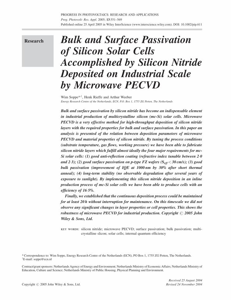
ton and toff are typically in the range of 10ms. In Figure 3 the ion current for a NH3 plasma, measured with
Langmuir probes along the tube axis is shown. The probes are positioned about 15 cm from the quartz tube
and have a bias voltage of �15V. The lateral distribution of the ion current density is a direct measure of
the homogeneity of the plasma density along the tube axis, which has a length of 60 cm. It can be observed
that for a zone width of at least 50 cm, the homogeneity of the plasma density is better than � 10%. A higher
pressure results in a lower ion current because of a higher recombination of reactive species.
Deposition with the linear MW plasma source differs in two crucial aspects from remote plasma enhanced
chemical vapor deposition (RPECVD), as applied by ISFH14,49 using a Plasmalab 80 from Oxford Plasma Tech-
nology, albeit both systems work with microwaves. First, the plasma chemistry is different. The RPECVD is a
true remote process in the sense that the only NH3 is dissociated in the microwave plasma. SiH4 is dissociated
only by interactions with NHx radicals. In the linear MW source, silane molecules can diffuse into the plasma
zone and will be dissociated by NHx radicals and by electrons. Second, the deposition geometry is different. For
RPECVD deposition emanates from a point source, resulting in reduced uniformity in comparison with the
linear MW source.
2.3 Growth rate and growth mechanisms
The growth rate of the SiNx:H layers normally depends on process parameters such as gas flow, pressure, and
temperature. We found that the growth rate of the SiNx:H layer in our system primarily depends on the total flow
of process gases, and depends only very little on process pressure or temperature. In principle, the growth rate
also depends on the microwave power, but in a linear MW system the practical range of the MW power that can
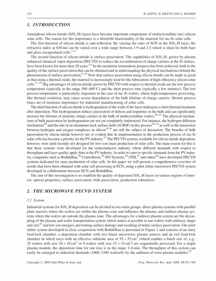
be applied is strongly restricted by homogeneity requirements. In Figure 4 the growth rate as a function of the
total flow for a fixed ratio of process gases NH3 and SiH4 is displayed. It can be seen that the growth rate
increases linearly with the total gas flow. This indicates that the growth rate—due to the high gas utiliza-
tion—is limited by the supply of precursor gases. The applied MW power apparently is not a limiting factor
in the production of reactive species in the flow range investigated.
Little is known yet about the details of the chemical reactions in the plasma in the microwave PECVD sys-
tem. A model for NH3/SiH4 plasmas has been proposed by Smith,50 and Hanyaloglu and Aydil51 and Kessels
et al.52 have proposed two similar models for N2/SiH4 plasmas.
For NH3/SiH4 plasmas the gases will be dissociated in NHx and SiHx species. It has been speculated by Smith
that these species combine in the plasma into tetraaminosilane Si(NH2)4 which acts as the main precursor for
layer growth. In this model the formation of Si(NH2)4 is the rate-limiting step. This model therefore predicts an
increase of the growth rate with increasing pressure, which is not in correspondence with our observations.
Figure 3. Ion current for NH3 plasma, measured with Langmuir probes along the tube axis, for two different pressures. The
probes are positioned about 15 cm from the quartz tube and have a bias voltage of �15V. The dashed line presents the ion
current at a higher pressure
BULK AND SURFACE PASSIVATION BY SILICON NITRIDE PECVD 555
Copyright # 2005 John Wiley & Sons, Ltd. Prog. Photovolt: Res. Appl. 2005; 13:551–569
Hanyalogly and Aydil suggested that in N2/SiH4 plasmas, silicon nitride layer growth proceeds through
attachment of SiH3 species to the surface followed by nitridation of the top of the film by vibrationally excited
N2 species. Kessels et al. conclude that the surface layer is nitrided by N radicals rather then by excited N2.
According to these growth models, the deposition rate depends on the flux of species arriving at the substrate.
Since the densities of N and SiH3 species depend on the production rate of these species and therefore on the
flow of the precursor gases, we conclude that the models of Hanyaloglu and Kessels can be reconciled with our
observations for microwave PECVD.
In the next sections we will evaluate the models mentioned with respect to other observations.
3. OPTICAL PROPERTIES OF SiN LAYERS
In order to function as an anti-reflection coating on crystalline Si solar cells, the silicon nitride layers should
have a refractive index of either about 2�0 or 2�3, for respectively bare cells and encapsulated cells.1 In addition,the absorption of light in the layers should be as small as possible for wavelengths where the solar cell is active
(300–1150 nm). This means that the optical bandgap of the SiNx:H should be larger than about 4 eV. Concisely:
the total transmittance T(�)¼ 1�R(�)�A(�) should be as large as possible for wavelengths between 300 and
1150 nm.
For stoichiometric silicon nitride with a refractive index of about 1�9, the optical bandgap53 is 5�3 eV. Theoptical gap decreases with increasing silicon contents until finally an optical gap of 1�8 eV for hydrogenated
amorphous silicon is obtained.54 The decrease of the optical gap is due to an increase of the Si–Si coordination
number and this increase produces narrowing of the Si–Si � and �* bands.53
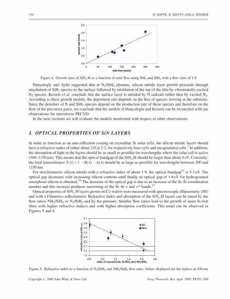
Optical properties of SiNx:H layers grown on Cz-wafers were measured with spectroscopic ellipsometry (SE)
and with a Filmetrics reflectometer. Refractive index and absorption of the SiNx:H layers can be tuned by the
flow ratios NH3/SiH4 or N2/SiH4 and by the pressure. Smaller flow ratios lead to the growth of more Si-rich
films with higher refractive indices and with higher absorption coefficients. This trend can be observed in
Figures 5 and 6.
Figure 5. Refractive index as a function of N2/SiH4 and NH3/SiH4 flow ratio. Values displayed are the indices at 630 nm
Figure 4. Growth rates of SiNx:H as a function of total flow using NH3 and SiH4 with a flow ratio of 1�0
556 W. SOPPE, H. RIEFFE AND A. WEEBER
Copyright # 2005 John Wiley & Sons, Ltd. Prog. Photovolt: Res. Appl. 2005; 13:551–569
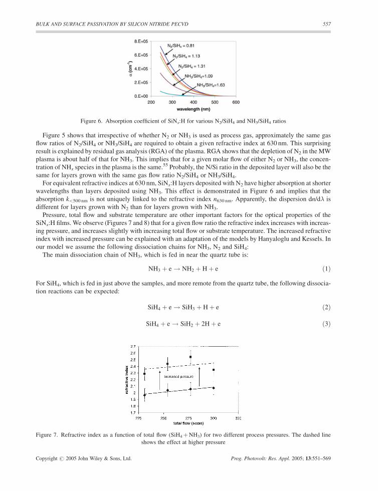
Figure 5 shows that irrespective of whether N2 or NH3 is used as process gas, approximately the same gas
flow ratios of N2/SiH4 or NH3/SiH4 are required to obtain a given refractive index at 630 nm. This surprising
result is explained by residual gas analysis (RGA) of the plasma. RGA shows that the depletion of N2 in the MW
plasma is about half of that for NH3. This implies that for a given molar flow of either N2 or NH3, the concen-
tration of NHx species in the plasma is the same.55 Probably, the N/Si ratio in the deposited layer will also be the
same for layers grown with the same gas flow ratio N2/SiH4 or NH3/SiH4.
For equivalent refractive indices at 630 nm, SiNx:H layers deposited with N2 have higher absorption at shorter
wavelengths than layers deposited using NH3. This effect is demonstrated in Figure 6 and implies that the
absorption k<500 nm is not uniquely linked to the refractive index n630 nm. Apparently, the dispersion dn/d� is
different for layers grown with N2 than for layers grown with NH3.
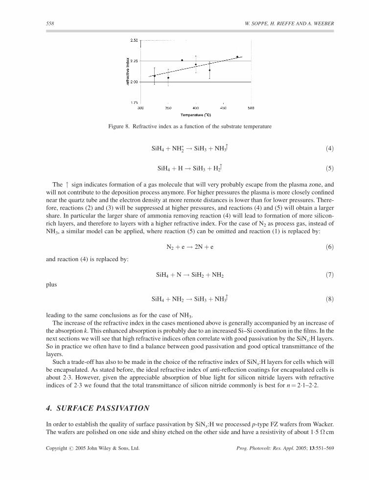
Pressure, total flow and substrate temperature are other important factors for the optical properties of the
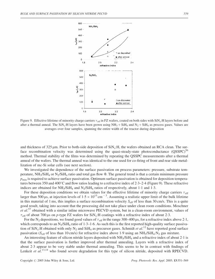
SiNx:H films. We observe (Figures 7 and 8) that for a given flow ratio the refractive index increases with increas-
ing pressure, and increases slightly with increasing total flow or substrate temperature. The increased refractive
index with increased pressure can be explained with an adaptation of the models by Hanyaloglu and Kessels. In
our model we assume the following dissociation chains for NH3, N2 and SiH4:
The main dissociation chain of NH3, which is fed in near the quartz tube is:
NH3 þ e ! NH2 þ Hþ e ð1Þ
For SiH4, which is fed in just above the samples, and more remote from the quartz tube, the following dissocia-
tion reactions can be expected:
SiH4 þ e ! SiH3 þ Hþ e ð2Þ
SiH4 þ e ! SiH2 þ 2Hþ e ð3Þ
Figure 6. Absorption coefficient of SiNx:H for various N2/SiH4 and NH3/SiH4 ratios
Figure 7. Refractive index as a function of total flow (SiH4þNH3) for two different process pressures. The dashed line
shows the effect at higher pressure
BULK AND SURFACE PASSIVATION BY SILICON NITRIDE PECVD 557
Copyright # 2005 John Wiley & Sons, Ltd. Prog. Photovolt: Res. Appl. 2005; 13:551–569
SiH4 þ NH�2 ! SiH3 þ NH3
" ð4Þ
SiH4 þ H ! SiH3 þ H2" ð5Þ
The " sign indicates formation of a gas molecule that will very probably escape from the plasma zone, and
will not contribute to the deposition process anymore. For higher pressures the plasma is more closely confined
near the quartz tube and the electron density at more remote distances is lower than for lower pressures. There-
fore, reactions (2) and (3) will be suppressed at higher pressures, and reactions (4) and (5) will obtain a larger
share. In particular the larger share of ammonia removing reaction (4) will lead to formation of more silicon-
rich layers, and therefore to layers with a higher refractive index. For the case of N2 as process gas, instead of
NH3, a similar model can be applied, where reaction (5) can be omitted and reaction (1) is replaced by:
N2 þ e ! 2Nþ e ð6Þand reaction (4) is replaced by:
SiH4 þ N ! SiH2 þ NH2 ð7Þplus
SiH4 þ NH2 ! SiH3 þ NH3" ð8Þ
leading to the same conclusions as for the case of NH3.
The increase of the refractive index in the cases mentioned above is generally accompanied by an increase of
the absorption k. This enhanced absorption is probably due to an increased Si–Si coordination in the films. In the
next sections we will see that high refractive indices often correlate with good passivation by the SiNx:H layers.
So in practice we often have to find a balance between good passivation and good optical transmittance of the
layers.
Such a trade-off has also to be made in the choice of the refractive index of SiNx:H layers for cells which will
be encapsulated. As stated before, the ideal refractive index of anti-reflection coatings for encapsulated cells is
about 2�3. However, given the appreciable absorption of blue light for silicon nitride layers with refractive
indices of 2�3 we found that the total transmittance of silicon nitride commonly is best for n¼ 2�1–2�2.
4. SURFACE PASSIVATION
In order to establish the quality of surface passivation by SiNx:H we processed p-type FZ wafers from Wacker.
The wafers are polished on one side and shiny etched on the other side and have a resistivity of about 1�5 � cm
Figure 8. Refractive index as a function of the substrate temperature
558 W. SOPPE, H. RIEFFE AND A. WEEBER
Copyright # 2005 John Wiley & Sons, Ltd. Prog. Photovolt: Res. Appl. 2005; 13:551–569
and thickness of 325 mm. Prior to both-side deposition of SiNx:H, the wafers obtained an RCA clean. The sur-
face recombination velocity was determined using the quasi-steady-state photoconductance (QSSPC)56
method. Thermal stability of the films was determined by repeating the QSSPC measurements after a thermal
anneal of the wafers. The thermal anneal was identical to the one used for co-firing of front and rear side metal-
lization of mc-Si solar cells (see next section).
We investigated the dependence of the surface passivation on process parameters: pressure, substrate tem-
perature, NH3/SiH4 or N2/SiH4 ratio and total gas flow �. The general trend is that a certain minimum pressure
pmin is required to achieve surface passivation. Optimum surface passivation is obtained for deposition tempera-
tures between 350 and 400�C and flow ratios leading to a refractive index of 2�3–2�4 (Figure 9). These refractiveindices are obtained for NH3/SiH4 and N2/SiH4 ratios of respectively, about 1�1 and 1�3.
For these deposition conditions we obtain values for the effective lifetime of minority charge carriers �efflarger than 500 ms, at injection levels of 1�5� 1015 cm� 3. Assuming a realistic upper limit of the bulk lifetime
in this material of 1ms, this implies a surface recombination velocity Seff of less than 30 cm/s. This is a quite
good result, taking into account that the processing did not take place under clean room conditions. Moschner
et al.57 obtained with a similar inline microwave PECVD system, but in a clean-room environment, values of
�eff of about 700 ms on p-type FZ wafers for SiNx:H coatings with a refractive index of about 2�3.For the N2 depositions, we found good values of �eff in the range 300–400 ms, for a refractive index above 2�1,
which corresponds to an N2/SiH4 ratio of 1�3–1�6. As such this is the first reported high-quality surface passiva-tion of SiNx:H obtained with only N2 and SiH4 as precursor gases. Schmidt et al.12 have reported good surface
passivation (Seff of less than 10 cm/s) for refractive index above 1�9 using an NH3/SiH4:N2 gas mixture.
An interesting feature of silicon nitride layers deposited with NH3/SiH4 and a refractive index of about 2�1 isthat the surface passivation is further improved after thermal annealing. Layers with a refractive index of
about 2�3 appear to be very stable under thermal annealing. This seems to be in contrast with findings of
Lenkeit et al.13,14 who found severe degradation for this type of silicon nitride, deposited with RPECVD.
Figure 9. Effective lifetime of minority charge carriers �eff in FZ wafers, coated on both sides with SiNx:H layers before and
after a thermal anneal. The SiNx:H layers have been grown using NH3þ SiH4 and N2þ SiH4 as process gases. Values are
averages over four samples, spanning the entire width of the reactor during deposition
BULK AND SURFACE PASSIVATION BY SILICON NITRIDE PECVD 559
Copyright # 2005 John Wiley & Sons, Ltd. Prog. Photovolt: Res. Appl. 2005; 13:551–569
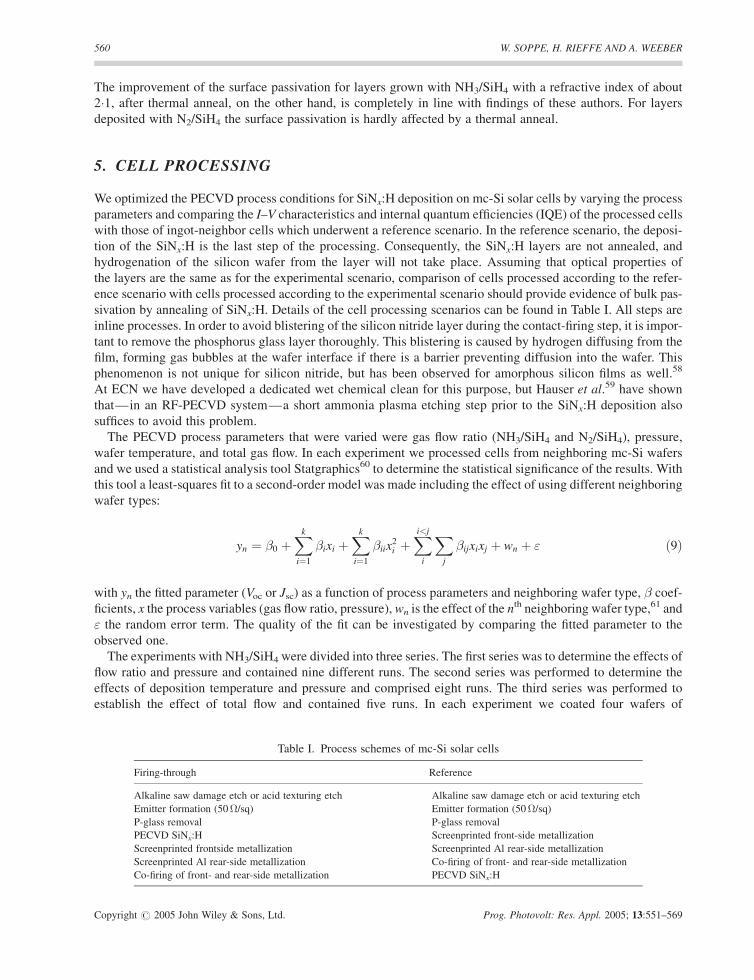
The improvement of the surface passivation for layers grown with NH3/SiH4 with a refractive index of about
2�1, after thermal anneal, on the other hand, is completely in line with findings of these authors. For layers
deposited with N2/SiH4 the surface passivation is hardly affected by a thermal anneal.
5. CELL PROCESSING
We optimized the PECVD process conditions for SiNx:H deposition on mc-Si solar cells by varying the process
parameters and comparing the I–V characteristics and internal quantum efficiencies (IQE) of the processed cells
with those of ingot-neighbor cells which underwent a reference scenario. In the reference scenario, the deposi-
tion of the SiNx:H is the last step of the processing. Consequently, the SiNx:H layers are not annealed, and
hydrogenation of the silicon wafer from the layer will not take place. Assuming that optical properties of
the layers are the same as for the experimental scenario, comparison of cells processed according to the refer-
ence scenario with cells processed according to the experimental scenario should provide evidence of bulk pas-
sivation by annealing of SiNx:H. Details of the cell processing scenarios can be found in Table I. All steps are
inline processes. In order to avoid blistering of the silicon nitride layer during the contact-firing step, it is impor-
tant to remove the phosphorus glass layer thoroughly. This blistering is caused by hydrogen diffusing from the
film, forming gas bubbles at the wafer interface if there is a barrier preventing diffusion into the wafer. This
phenomenon is not unique for silicon nitride, but has been observed for amorphous silicon films as well.58
At ECN we have developed a dedicated wet chemical clean for this purpose, but Hauser et al.59 have shown
that—in an RF-PECVD system—a short ammonia plasma etching step prior to the SiNx:H deposition also
suffices to avoid this problem.
The PECVD process parameters that were varied were gas flow ratio (NH3/SiH4 and N2/SiH4), pressure,
wafer temperature, and total gas flow. In each experiment we processed cells from neighboring mc-Si wafers
and we used a statistical analysis tool Statgraphics60 to determine the statistical significance of the results. With
this tool a least-squares fit to a second-order model was made including the effect of using different neighboring
wafer types:
yn ¼ �0 þXk
i¼1
�ixi þXk
i¼1
�iix2i þ
Xi<j
i
X
j
�ijxixj þ wn þ " ð9Þ
with yn the fitted parameter (Voc or Jsc) as a function of process parameters and neighboring wafer type, � coef-
ficients, x the process variables (gas flow ratio, pressure), wn is the effect of the nth neighboring wafer type,61 and
" the random error term. The quality of the fit can be investigated by comparing the fitted parameter to the
observed one.
The experiments with NH3/SiH4 were divided into three series. The first series was to determine the effects of
flow ratio and pressure and contained nine different runs. The second series was performed to determine the
effects of deposition temperature and pressure and comprised eight runs. The third series was performed to
establish the effect of total flow and contained five runs. In each experiment we coated four wafers of
Table I. Process schemes of mc-Si solar cells
Firing-through Reference
Alkaline saw damage etch or acid texturing etch Alkaline saw damage etch or acid texturing etch
Emitter formation (50�/sq) Emitter formation (50�/sq)
P-glass removal P-glass removal
PECVD SiNx:H Screenprinted front-side metallization
Screenprinted frontside metallization Screenprinted Al rear-side metallization
Screenprinted Al rear-side metallization Co-firing of front- and rear-side metallization
Co-firing of front- and rear-side metallization PECVD SiNx:H
560 W. SOPPE, H. RIEFFE AND A. WEEBER
Copyright # 2005 John Wiley & Sons, Ltd. Prog. Photovolt: Res. Appl. 2005; 13:551–569

12�5� 12�5 cm2 or five wafers of 10� 10 cm2. We used neighbor wafers to ensure equal run-to-run wafer mate-
rial quality in each experiment.
The depositions with N2/SiH4 comprised one experiment of 16 runs in which we applied 12�5� 12�5 cm2
wafers, and coated 4 wafers per deposition. An acid etch was applied for saw damage removal and texturing.
We used 4 sets of 16 neighbors to determine the effects of process pressure, flow ratio and total flow on the solar
cell performances.
5.1 Effects of flow ratio
Changing the ratio of NH3/SiH4 or N2/SiH4 is the most straightforward way to vary the N/Si ratio in the film.
The N/Si ratio in the film determines the refractive index and strongly effects the surface passivation of the
SiNx:H layers. The so-called main effect of the flow ratio on the electrical performances of mc-Si cells is smal-
ler, but still significant, as illustrated in Figure 10 for NH3/SiH4 depositions and in Figure 11 for N2/SiH4
depositions. The inserts show plots of the observed Voc and Jsc against the fitted values. The observed values
scatter randomly around the observed¼ fitted line, justifying the model used.
Highest Voc is obtained for silicon rich layers (obtained with small NH3/SiH4 or N2/SiH4 ratios) and this is at
least partly due to optimum surface passivation for Si-rich layers. The current, however, depends strongly on the
optical properties of the layers. The ideal refractive index of AR coatings on cells (in air) is about 2�1–2�2, andthis value is obtained for higher NH3/SiH4 or N2/SiH4 ratios of about 1�6.
For highest cell efficiencies a compromise is required between conditions for high Voc and high Jsc. For
depositions with NH3 and SiH4 this leads to maximum Voc� Jsc for NH3/SiH4’ 1�6. For depositions with
N2 and SiH4 we find maximum Voc� Jsc for N2/SiH4’ 1�5.
5.2 Effect of pressure
The process pressure affects the chemistry in the plasma by affecting the radius of the plasma zone and by
affecting the residence time of process gases. As a result the composition of the SiNx:H layers and their passi-
vating properties vary with varying process pressures.
For cell processing with SiNx:H layers grown with NH3 and SiH4, an optimum deposition pressure was estab-
lished. For lower pressures the bulk passivation is reduced which affects both Voc and Jsc. For higher pressures
Voc saturates but Jsc decreases due to absorption as a result of the higher refractive index. These effects can be
seen in Figure 12. Note that the IQEs are corrected for reflection of the silicon nitride layers, but not for the
absorption of these layers.
Figure 10. Main effect of the NH3/SiH4 flow ratio on Jsc and Voc of mc-Si cells, fabricated with firing-through SiNx:H layers.
Statistics show that the effect on Jsc is real with a certainty of 90% (More precisely: the effect is different from zero at the
90% confidence limit). For Voc the certainty is more than 95%. The inserts show the observed versus the fitted values for Vocand Jsc
BULK AND SURFACE PASSIVATION BY SILICON NITRIDE PECVD 561
Copyright # 2005 John Wiley & Sons, Ltd. Prog. Photovolt: Res. Appl. 2005; 13:551–569

5.3 Effect of substrate temperature
We varied the substrate temperature between 325 and 400�C, and within this range the temperature did not
affect the cell performances. From previous experiments25 we know that the hydrogen content decreases and
the surface passivation improves in general with increasing substrate temperature in the range 200–400�C, butin the range 325–400�C the changes are not significant.
Figure 13 illustrates these findings. The figure shows the IQEs of cells with SiNx:H coatings deposited at
various temperatures, relative to the IQE of a reference neighboring cell made (see Table I). The large increase
of IQE between 800 and 1200 nm is due to bulk passivation. The gain of IQE for the cell which obtained the
SiNx:H coating at 400�C is slightly smaller than for the lower substrate temperatures. This can be attributed to
slightly smaller hydrogen contents in the layers deposited at 400�C.The increase of IQE at smaller wavelengths between 350 and 450 nm suggests that the firing-through SiNx:H
process also leads to better passivation in the front surface region. The total gain of IQE leads to an increase of
Voc from 589mV for the reference cells to 612mV for the cells from the firing-through scenario.
5.4 Effects of total flow
The electrical performances of mc-Si solar cells are quite sensitive to the total flow during the silicon
nitride deposition in the case of NH3 and SiH4 as process gasses. We varied the total flow from 185 to 355 sccm,
Figure 11. Main effect of the N2/SiH4 flow ration on Jsc and Voc of mc-Si cells, fabricated with firing-through SiNx:H layers.
Statistics show that the effect on Jsc is real with a certainty of more than 95%. For Voc it is 85%. The inserts show the
observed versus the predicted values for Voc and Jsc
Figure 12. Relative internal quantum efficiencies of cells made with silicon nitride, grown with NH3 and SiH4, deposited at
various pressures. IQEs are relative to that of a cell that underwent the reference scenario. The lower pressure shows a
decreased red response and the higher pressure a decreased blue response
562 W. SOPPE, H. RIEFFE AND A. WEEBER
Copyright # 2005 John Wiley & Sons, Ltd. Prog. Photovolt: Res. Appl. 2005; 13:551–569

keeping the ratio NH3/SiH4 constant at 1�6. Voc increases with increasing total flows and Jsc has an optimum for
about 280 sccm. Best cell performances are found for a total flow of 280 sccm.
The effect of the flow rates for depositions with N2 and SiH4 was investigated in a narrower range: between
200 and 250 sccm. Within this range, the total flow does not have a significant effect on Voc or Jsc.
5.5 Overall effects
The optimum SiNx:H for the front side of mc-Si solar cells is the result of a delicate trade-off of various proper-
ties: total transmittance, surface passivation and bulk passivation. High transmittance requires a refractive index
of 1�9–2�1, which is obtained for N2/SiH4 and NH3/SiH4 ratios in the range 1�4–1�6. Best surface passivation ofFZ wafers is obtained for small flow ratios of 1�1, which results in a refractive index of about 2�3. These layersare highly absorbing.
Our experiments provide clear evidence for the capability of SiNx:H to improve the effective lifetime of min-
ority charge carriers in the bulk of mc-Si wafers (bulk passivation) if the layer is annealed as in the firing process
of screenprinted metallization.
The most favorable SiNx:H layer thus is a compromise, but nevertheless it is a very effective layer. In com-
parison with the non-passivating alternative: the formerly commonly used TiO2 layer, application of SiNx:H
typically leads to a gain of 20mV and an increase of 10–15% of the total cell performance.
Results of I–V measurements of the cells obtained for optimum deposition conditions are displayed in
Table II. The results underline the importance of front surface passivation in order to obtain high-efficiency
cells. By using different wafer material and more advanced processing, but using the same recipe for SiNx:H
deposition we were able to increase cell efficiencies from 14�7 to 16�5%. This improvement resulted merely
because the lower-doped emitter allowed better surface passivation, and therefore a significantly better internal
quantum efficiency at short wavelengths.
Figure 13. Relative internal quantum efficiencies of cells made with silicon nitride deposited at various substrate
temperatures. NH3 and SiH4 were used as process gases. IQEs are relative to that of a cell that underwent the reference
scenario
Table II. I–V characteristics of mc-Si cells with SiNx:H deposition, obtained for optimum deposition conditions
Process gas Emitter sheet Jsc (mA/cm2) Voc (mV) Jsc�Voc (mA/cm2V) Efficiency (%)
resistance (�/sq)NH3 N2
� 50 32�1 605 19�4 14�7� 50 32�3 600 19�4 14�7
� 65 34�5 623 21�5 16�5
Values in the first two rows are means over four cells (12�5� 12�5 cm), covering the entire width of the deposition tray. The last row shows
the results of the best cell, measured at NREL, using a more advanced inline processing and Si wafers from another batch, but with the same
SiNx:H deposition process as for the first row.
BULK AND SURFACE PASSIVATION BY SILICON NITRIDE PECVD 563
Copyright # 2005 John Wiley & Sons, Ltd. Prog. Photovolt: Res. Appl. 2005; 13:551–569
6. STABILITY OF PECVD PROCESS
We have performed an endurance test to check the stability of the microwave PECVD process over a long per-
iod of use. Important topics we wanted to investigate were:
1. What is the total deposition time that a system can run continuously without flake formation? The MW-PECVD system has a downstream configuration: the tray with wafers moves underneath the quartz tubes.Because of that, silicon nitride flakes formed by parasitic deposition can fall on the wafers. Large flakes orlarge numbers of small flakes will result in visually unacceptable cells. Moreover, solar cell efficiency losseswill occur due to reflection losses. A drastic solution is to apply an upstream configuration, but this results insmall uncoated areas on all wafers due to shadowing by suspension clamps.
2. Do the passivation properties change with increasing deposition time? These properties could changebecause of small changes in the plasma due to parasitic depositions.
We used an industrial process scheme for making solar cells as discussed in Section 5. Multicrystalline
12�5� 12�5 cm wafers were used as starting material. The wafers were distributed over 19 batches. We used
neighboring wafers to exclude differences in material quality. After different times of plasma processing a batch
of wafers was deposited using the standard ECN process with NH3 and SiH4 as process gasses. Together with
the multicrystalline wafers a piece of polished monocrystalline material was deposited for optical characteriza-
tion of the SiNx:H layer. After about 8 h plasma processing the system was cooled down to room temperature
during the night. After heating up on the next day the processing was resumed. After about 17 h there was
another break during night. The total time with plasma on was 20 h.
6.1 Number of flakes and optical properties
During the first period of about 8 h plasma time hardly any flakes fall from the quartz tubes or from the walls of
the system on the wafers. During the nights the system was cooled down. The first deposition the next day
showed a larger number of small flakes on the wafers. However, the number of flakes reduced tremendously
after a second deposition. The same was observed for the next day.
In an industrial environment the system will probably not be cooled down during normal operation and this
effect will be of little importance.
The refractive index nmeasured at 630 nm was 2�10 and constant over 20 h plasma time. The extinction coef-
ficient k did not change either. However, the layer thickness increased a few nanometer, but the increase is less
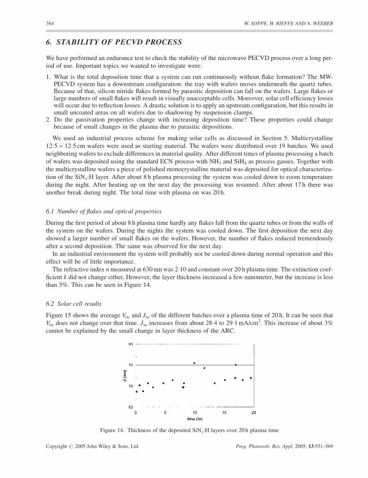
than 5%. This can be seen in Figure 14.
6.2 Solar cell results
Figure 15 shows the average Voc and Jsc of the different batches over a plasma time of 20 h. It can be seen that
Voc does not change over that time. Jsc increases from about 28�4 to 29�1mA/cm2. This increase of about 3%
cannot be explained by the small change in layer thickness of the ARC.
Figure 14. Thickness of the deposited SiNx:H layers over 20 h plasma time
564 W. SOPPE, H. RIEFFE AND A. WEEBER
Copyright # 2005 John Wiley & Sons, Ltd. Prog. Photovolt: Res. Appl. 2005; 13:551–569
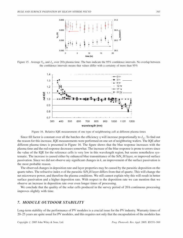
Since fill factor is constant over all the batches the efficiency � will increase proportionally to Jsc. To find outthe reason for this increase, IQE measurements were performed on one set of neighboring wafers. The IQE after
different plasma times is presented in Figure 16. The figure shows that the blue response increases with the
plasma time and the red response decreases somewhat. The increase of the blue response is prone to errors since
the value of the IQE for the reference cells is very low in this wavelength region, but seems nonetheless sys-
tematic. The increase is caused either by enhanced blue transmittance of the SiNx:H layer, or improved surface
passivation. Since we did not observe any significant changes in k, an improvement of the surface passivation is
the most probable reason.
The observed changes in deposition rate and layer properties may be caused by the parasitic deposition on the
quartz tubes. The refractive index n of the parasitic SiNxH layer differs from that of quartz. This will change the
net microwave power, and therefore the plasma conditions. We still cannot explain why this will result in better
surface passivation and a higher deposition rate. With respect to the deposition rate we can mention that we
observe an increase in deposition rate over even longer times of processing.
We conclude that the quality of the solar cells produced in the survey period of 20 h continuous processing
improves slightly with time.
7. MODULE OUTDOOR STABILITY
Long-term stability of the performance of PV modules is a crucial issue for the PV industry. Warranty times of
20–25 years are quite usual for PV modules, and this requires not only that the encapsulation of the modules has
Figure 15. Average Voc and Jsc over 20 h plasma time. The bars indicate the 95% confidence intervals. No overlap between
the confidence intervals means that values differ with a certainty of more than 95%
Figure 16. Relative IQE measurement of one type of neighbouring cell at different plasma times
BULK AND SURFACE PASSIVATION BY SILICON NITRIDE PECVD 565
Copyright # 2005 John Wiley & Sons, Ltd. Prog. Photovolt: Res. Appl. 2005; 13:551–569

to be very well weather resistant (e.g., to prevent corrosion of electrical contacts, and delamination of EVA) but
also that the electrical performance of the cells has to be stable on a long-term basis.62 The key issue for the
silicon nitride layers in this respect is the stability of the passivating properties under long-term irradiation. In
particular the UV stability of the surface passivation has been a source of concern in the past.7
In order to monitor the long-term stability of cells with a SiNx:H coating deposited by MW-PECVD, a mod-
ule was manufactured at ECN in July 2000 in which 36mc-Si cells were incorporated. The cells were made
from 10� 10 cm Baysix wafers, using a standard processing at ECN, as described in Section 5. The SiNx:H
coating was deposited using NH3 and SiH4 at conditions close to the optimum ones found in Section 6, using
the system described in Section 2. The module was encapsulated with glass and EVA on the front side and
Tedlar# at the rear side. After manufacturing, the module was placed on the roof of the ECN Solar Energy
office building in Petten, and was regularly measured by an indoor flash-tester at ECN. The results of this mon-
itoring are shown in Figure 17. It can be observed that the performance of the module was very stable over the
entire monitoring period that lasted more than 2 years. A slight decrease of Jsc is found, but this decrease is
partially compensated by a small increase of Voc. The origin of the small increase of Voc is unclear so far,
but we may conclude that the cells—and therefore the SiNx:H coatings—do not degrade during outdoor illu-
mination. The power degradation over 2 years is less than 2% which is better than the 1-year average of 4�2% of
98 commercially available c-Si modules tested at LEEE-TISO.63
8. CONCLUSIONS
SiNx:H coatings have become crucial components of commercial mc-Si solar cells. ECN and Roth&Rau Ober-
flachentechnik have jointly developed an industrial scale microwave PECVD system for deposition of such
SiNx:H layers. The layers have to fulfill three major requirements: (1) enhancement of the transmittance of light,
by reduction of the reflection; (2) surface passivation; and (3) bulk passivation. The optimum SiNx:H layer is a
trade-off result of these three requirements, and therefore depends to some extent on other aspects of the cell.
The emitter dopant concentration, e.g., determines the need and the effectiveness of surface passivation and the
starting quality of the wafers determines the need and the effectiveness of bulk passivation.
We have shown that by using microwave PECVD, we are able to deposit SiNx:H layers fulfilling all three
requirements, both for N2/SiH4 and for NH3/SiH4 as process gases. Required optical properties can be obtained
by tuning the N2/SiH4 or NH3/SiH4 gas flow ratio. For N2/SiH4 depositions, somewhat lower pressures have to
be applied in order to achieve the same high total transmittance as for SiNx:H layers deposited with NH3/SiH4.
Best surface passivation is obtained for Si-rich layers, with a refractive index of 2�3 and higher, and this passi-
vation is thermally stable for layers grown with N2/SiH4 and with NH3/SiH4. Effective recombination velocities
on p-type FZ wafers coated with such layers are below 30 cm/s. Reasonably good surface passivation after ther-
mal anneal (with Seff on p-type FZ wafers in the range of 100 cm/s) can be obtained for layers with a refractive
index of about 2�2. This latter result is of great practical relevance since the layers also have to provide bulk
passivation by thermally enhanced hydrogenation of the wafers in the fabrication process of mc-Si wafers.
Figure 17. Two-year I–V monitoring results of module placed outdoors. Irradiance of the flash-tester was 1000W/m2
566 W. SOPPE, H. RIEFFE AND A. WEEBER
Copyright # 2005 John Wiley & Sons, Ltd. Prog. Photovolt: Res. Appl. 2005; 13:551–569
Good bulk passivation requires that the SiNx:H layers are deposited at a certain minimum pressure. We have
found a significant improvement of IQE between 900 and 1200nm as a result of bulk passivation induced by firing
of SiNx:H layers. This improvement of the bulk lifetime of charge carriers leads to a gain of 20mVand an increase
of 10–15% of the total cell performance in comparison with cells on which a non-passivating TiO2 layer was depos-
ited as anti-reflection coating. Using an optimized SiNx:H deposition process in a typically industrial inline fabri-
cation process of mc-Si solar cells we have been able to produce cells with an efficiency of 16�5%.
We have shown that the deposition process, using microwave PECVD is a robust and stable process, in which
optical properties and deposition rate varies less than 5% in a continuous processing period of 20 h.
For practical purposes, it is important that the SiNx:H layers are stable on a long-term basis. Outdoor module
stability experiments show that the passivating properties of SiNx:H, deposited by microwave PECVD do not
show any significant degradation after a time span of more than 2 years.
Acknowledgements
This work has been financed by the Netherlands Agency of Energy and Environment (NOVEM) in the projects
ProDuSi and TOPR, and within the E.E.T. program by the Ministry of Economic Affairs, the Ministry of Edu-
cation, Culture and Science and the Ministry of Public Housing, Physical Planning and Environment in the
project Sunovation. The authors wish to thank Hermann Schlemm (Roth&Rau) for plasma density measure-
ments and Junegie Hong (Eindhoven University of Technology) for measurements of optical properties of sili-
con nitride layers. Eric Kossen, Martien Koppes and Hans ter Beeke are thanked for technical assistance. Wim
Sinke is acknowledged for the fruitful discussions on the presented work. Tom Moriarty and Keith Emery of
NREL are acknowledged for performing I–V measurements.
REFERENCES
1. Doshi P, Jellison GE, Rohatgi A. Characterization and optimization of absorbing PECVD antireflection coatings for
silicon photovoltaics. Journal of Applied Optics 1997; 36: 7826.
2. Nagel H, Aberle AG, Hezel R. Optimised antireflection coatings for planar silicon solar cells using remote PECVD
silicon nitride and porous silicon dioxide. Progress in Photovoltaics: Research and Applications 1999; 7: 245–260.
3. Winderbaum S, Yun F, Reinhold O. Application of plasma enhanced chemical vapor deposition silicon nitride as a
double layer antireflection coating and passivation layer for polysilicon solar cells. Journal of Vacuum Science and
Technology 1997; A15: 1020–1025.
4. Hezel R, Schorner R. Plasma silicon nitride—a promising dielectric to achieve high-quality silicon MIS/IL solar cells.
Journal of Applied Physics 1981; 52: 3076.
5. Hezel R, Blumenstock K, Schorner R. Interface states and fixed charges in MNOS structures with APCVD and plasma
silicon nitride. Journal of the Electrochemical Society 1984; 131: 1679.
6. Leguijt C. Surface Passivation for Silicon Solar Cells. Thesis, Utrecht University, 1995.
7. Schuurmans F. Surface Passivation of Silicon by PECVD Silicon Nitride. Thesis, Utrecht University, 1998.
8. Schmidt J. Untersuchungen zur Ladungstragerrekombination and den Oberflachen und im Volumen von kristallinen
Silicium-Solarzellen. Thesis, Hannover University, 1998.
9. Aberle AG, Hezel R. Progress in low-temperature surface passivation of silicon solar cells using remote-plasma silicon
nitride. Progress in Photovoltaics: Research and Applications 1997; 5: 29–50.
10. Aberle AG. Crystalline Silicon Solar Cells: Advanced Surface Passivation and Analysis. The University of New South
Wales, 1999.
11. Schmidt J, Aberle AG. Carrier recombination at silicon–silicon nitride interfaces fabricated by plasma-enhanced
chemical vapor deposition. Journal of Applied Physics 1999; 85: 3626–3633.
12. Schmidt J, Kerr M. Highest-quality surface passivation of low-resistivity p-type silicon using stoichiometric PECVD
silicon nitride. Solar Energy Materials and Solar Cells 2001; 65: 585–591.
13. Lenkeit B, Hezel R. Improved understanding of the surface-passivating properties of RPECVD silicon nitride on p-type
crystalline silicon. Proceedings of the 17th European Photovoltaic Solar Energy Conference, Munich, Germany, 22–26
October 2001; 343–346.
BULK AND SURFACE PASSIVATION BY SILICON NITRIDE PECVD 567
Copyright # 2005 John Wiley & Sons, Ltd. Prog. Photovolt: Res. Appl. 2005; 13:551–569
14. Lenkeit B, Steckemetz S, Artuso F, Hezel R. Excellent thermal stability of remote plasma-enhanced chemical vapour
deposited silicon nitride films for the rear of screen-printed bifacial silicon solar cells. Solar Energy Materials and Solar
Cells 2001; 65: 317–323.
15. Mackel H, Ludemann R. Detailed study of the composition of hydrogenated SiNx layers for high-quality silicon surface
passivation. Journal of Applied Physics 2002; 92: 2602–2609.
16. Cuevas A, Kerr M, Schmidt J. Passivation of crystalline silicon using silicon nitride. Proceedings of the 3rd World
Conference on Photovoltaic Energy Conversion, Osaka, Japan, 11–18 May 2003; 913–918.
17. Kimura K. Recent developments in polycrystalline silicon solar cells. Technical Digest, International PVSEC-1, Kobe,
November 1984; 3741.
18. Schmidt J, Kerr M, Cuevas A. Surface passivation of silicon solar cells using plasma-enhanced chemical-vapour-deposited
SiN films and thin thermal SiO2/plasma SiN stacks. Semiconductor Science and Technology 2001; 16: 164–170.
19. Mittelstadt L, Dauwe S, Metz A, Hezel R, Hassler C. Front and rear silicon-nitride-passivated multicrystalline silicon
solar cells with an efficiency of 18�1%. Progress in Photovoltaics: Research and Applications 2002; 10: 35–39.
20. Chen Z, Rohatgi A, Bell RO, Kalejs JP. Defect passivation in multicrystalline-Si materials by plasma-enhanced chemical
vapor deposition of SiO2/SiN coatings. Applied Physics Letters 1994; 65: 2078–2080.
21. Duerinckx F. Bulk and surface passivation of screen printed multicrystalline silicon solar cells based on plasma
enhanced CVD of silicon nitride. Thesis, Leuven University, 1999.
22. Einhaus R, Duerinckx F, Van Kerschaver E, Szlufcik J, Durand F, Riberyron PJ, Duby JC, Sarti D, Goaer G, Le GN,
Perichaud I, Clerc L, Martinuzzi S. Hydrogen passivation of newly developed EMC-multi-crystalline silicon.Materials
Science and Engineering 1999; B58: 81–85.
23. Jeong JW, Rosenblum MD, Kalejs JP, Rohatgi A. Hydrogenation of defects in edge-defined film-fed grown aluminum-
enhanced plasma enhanced chemical vapor deposited silicon nitride multicrystalline silicon. Journal of Applied Physics
2000; 87: 7551–7557.
24. SoppeW,Weeber A, de Moor H, Sinke W, Lauinger T, Auer R, Lenkeit B, Aberle A. Cost effective mc-Si processing by
screenprinting on remote PECVD layers. Proceedings of the 2nd World Conference and Exhibition on Photovoltaic
Solar Energy Conversion, Vienna, Austria, 6–10 July 1998; 1826–1828.
25. Soppe WJ, Devilee C, Schiermeier SEA, Hong J, Kessels WMM, Van de Sanden MCM, Arnoldbik WM, Weeber AW.
Bulk and surface passivation by silicon nitride grown by remote microwave PECVD. Proceedings of the 17th European
Photovoltaic Solar Energy Conference, Munich, Germany, 22–26 October 2001; 1543–1546.
26. Duerinckx F, Szlufcik J. Defect passivation of industrial multicrystalline solar cells based on PECVD silicon nitride.
Solar Energy Materials and Solar Cells 2002; 72: 231–246.
27. GeerligsLJ,AzziziA,MacdonaldDH,ManshandenP.Hydrogenpassivation of iron inmulticrystalline silicon.Proceedings of
the 13thWorkshop on Crystalline Silicon Solar Cell Materials and Processes, Colorado, USA, 10–13August 2003; 199–202.
28. Pankove JI, Johnson NM. Hydrogen in Semiconductors. Academic Press: New York, 1991.
29. Sopori BL, Deng X, Benner JP, Rohatgi A, Sana P, Estreicher SK, Park YK, Roberson MA. Hydrogen in silicon: a
discussion of diffusion and passivation mechanisms. Solar Energy Materials and Solar Cells 1996; 41/42: 159–169.
30. Nickel NH, Kaiser I. Hydrogen migration in phosphorous doped polycrystalline silicon. Materials Research Society
Symposium Proceedings 1998; 513: 165–170.
31. Boehme C, Lucovsky G. H loss mechanism during anneal of silicon nitride: chemical dissociation. Journal of Applied
Physics 2000; 88: 6055–6059.
32. Sopori B, Zhang Y, Ravindra NM. Silicon device processing in H-ambients: H-diffusion mechanisms and influence on
electronic properties. Journal of Electronic Materials 2001; 30: 1616–1627.
33. Rohatgi A, Yelundur V, Jeong J, Ebong A, Rosenblum MD, Hanoka JI. Fundamental understanding and implementation
of Al-enhanced PECVD SiNx hydrogenation in silicon ribbons. Solar Energy Materials and Solar Cells 2002; 74: 117–126.
34. Hong J, Kessels WMM, Soppe WJ, Weeber AW, Arnoldbik WM, Van de Sanden MCM. Influence of the high-
temperature ‘firing’ step on high-rate plasma deposited silicon nitride films used as bulk passivating antireflection
coatings on silicon solar cells. Journal of Vacuum Science Technology B 2003; 21: 2123–2132.
35. Job R, Fahrner WR, Kazuchits NM, Ulyashin AG. A two-step low-temperature process for a p–n junction formation due
to hydrogen enhanced thermal donor formation in p-type Czochralski silicon. Materials Research Society Symposium
Proceedings 1998; 513: 337–342.
36. Rashkeev SN, Di Ventra M, Pantelides ST. Hydrogen passivation and activation of oxygen complexes in silicon. Applied
Physics Letters 2001; 78: 1571–1573.
37. Aberle AG, Lauinger T, Hezel R. Remote PECVD silicon nitride—a key technology for the crystalline silicon PV
industry of the 21st century? Proceedings of the 14th European Photovoltaic Solar Energy Conference, Barcelona,
Spain, 30 June–4 July 1997; 684–689.
568 W. SOPPE, H. RIEFFE AND A. WEEBER
Copyright # 2005 John Wiley & Sons, Ltd. Prog. Photovolt: Res. Appl. 2005; 13:551–569

38. Soppe WJ, Duijvelaar BG, Schiermeier SEA, Weeber AW, Steiner A, Schuurmans FM. A high-throughput PECVD
reactor for deposition of passivating SiN layers. Proceedings of the 16th European Photovoltaic Solar Energy
Conference, Glasgow, UK, 1–5 May 2000; 1420–1423.
39. Schitthelm F, Volk P, Dekkers H, Szlufcik J. Quasi continuous a-SiN:H-PECVD system with high throughput rate for
solar cell AR-coating. Proceedings of the 16th European Photovoltaic Solar Energy Conference, Glasgow, UK, 1–5May
2000; 1609–1612.
40. Coates K, Morrison S, Narayanan S, Madan A. Deposition of silicon nitride to improve the conversion efficiency of
multicrystalline silicon solar cells. Proceedings of the 16th European Photovoltaic Solar Energy Conference, Glasgow,
UK, 1–5 May 2000; 1279–1281.
41. http://www.otb.nl/Media/Leaflet_DEPx_met_foto.pdf
42. Von Aichberger S. Deeper than blue.Market survey on deposition systems for silicon nitride. Photon International 2003;
3: 50–55.
43. Culik JS, Faller F, Goncharovsky IS, Rand JA, Barnett AM. Progress on 15 MW single thread silicon-filmTM solar cell
manufacturing systems. Proceedings of the 17th European Photovoltaic Solar Energy Conference, Munich, Germany,
22–26 October 2001; 1347–1350.
44. Nybergh K. Using factorial design and response surface methodology to optimize growth parameters of PECVD grown
silicon nitride. Physica Scripta 1999; T79: 266–271.
45. Moisan M, Pelletier J. Microwave Exited Plasmas. Elsevier: Amsterdam, 1992; 123–180.
46. Lieberman MA, Lichtenberg AJ. Principles of Plasma Discharges and Materials Processing. Wiley: New York, 1994.
47. Petasch W, Rauchle E, Muegge H, Muegge K. Duo plasmaline—a linearly extended homogeneous low pressure plasma
source. Surface and Coatings Technology 1997; 93: 112–118.
48. Rauchle E. Duo-plasmaline, a surface wave sustained linearly extended discharge. Journal de Physique IV France 1998;
8(Pr7): 99–107.
49. Lauinger T, Moschner J, Aberle AG, Hezel R. Optimization and characterization of remote plasma-enhanced chemical
vapor deposition silicon nitride for the passivation of p-type crystalline surfaces. Journal of Vacuum Science and
Technology A 1998; 16: 530–543.
50. Smith DL. Plasma deposition of SiNxHy: process chemistry vs film properties. Materials Research Society Symposium
Proceedings 1990; 165: 69–77.
51. Hanyaloglu BF, Aydil ES. Low temperature plasma deposition of silicon nitride from silane and nitrogen plasmas.
Journal of Vacuum Science and Technology 1998; A16: 2794–2803.
52. Kessels WMM, van Assche FJH, Hong J, SchrammDC, van de SandenMCM. Plasma diagnostic study of silicon nitride
film growth in a remote Ar-H2-N2-SiH4 plasma: role of N and SiHn radicals. Journal of Vacuum Science and Technology
A 2004; 22: 96–106.
53. Robertson J. Electronic structure of silicon nitride. Philosophical Magazine B 1991; 63: 47–77.
54. Giorgis F, Giuliani F, Pirri CF, Tesso E. Optical, structural and electrical properties of device quality hydrogenated
amorphous silicon-nitrogen films deposited by plasma-enhanced chemical vapour deposition. Philosophical Magazine
B 1998; 77: 925–944.
55. Rieffe HC, SoppeWJ, Kessels WMM, Van de SandenMCM,Weeber AW. Passivation on mc-Si solar cells with PECVD
SiNx:H using N2 and SiH4. Proceedings of PV in Europe from PV Technology to Energy Solutions, Rome, Italy, 7–11
October 2002; 295–298.
56. Sinton RA, Cuevas A. Contactless determination of current—voltage characteristics and minority-carrier lifetimes in
semiconductors from quasi-steady-state photoconductance data. Applied Physics Letters 1996; 69: 2510–2512.
57. Moschner JD, Henze J, Schmidt J, Hezel R. High-quality surface passivation of silicon solar cells in an industrial-type
inline plasma silicon nitride deposition system. Progress in Photovoltaics: Research and Applications 2004; 12: 21–31.
58. Shanks HR, Lye L. Formation of pin holes in hydrogenated amorphous silicon at high temperatures and the yield strength
of a-Si:H. Journal of Applied Physics 1981; 52: 811–813.
59. Hauser A, Spiegel M, Fath P, Bucher E. Influence of an ammonia activation prior to the PECVD SiN deposition on the
solar cell performance. Solar Energy Materials and Solar Cells 2003; 75: 357–362.
60. http://www.statgraphics.com
61. Weeber AW, SinkeWC. Statistical analysis for solar cell research.Proceedings of the 25th IEEE, WashingtonDC, 1996; 565.
62. IEC 61215. Crystalline silicon terrestrial photovoltaic (PV) modules—Design qualification and type approval 1993.
63. Chianese D, Realini A, Cereghetti N, Rezzonico S, Bura E, Friesen G, Bernasconi A. Analysis of weathered c-Si PV
modules. Proceedings of the 3rdWorld Conference on Photovoltaic Energy Conversion, Osaka, Japan, 11–18May 2003;
2922–2926.
BULK AND SURFACE PASSIVATION BY SILICON NITRIDE PECVD 569
Copyright # 2005 John Wiley & Sons, Ltd. Prog. Photovolt: Res. Appl. 2005; 13:551–569