b.supmonchai design rules
TRANSCRIPT

B.Supmonchai July 5th, 2004
2102-545 Digital ICs 1
Tutorial 1
Design Rules and Layout Techniques
Boonchuay SupmonchaiIntegrated Design Application Research (IDAR) Laboratory
July 5th, 2004
2102-545 Digital ICs Design Rules and Layout Techniques 2
B.Supmonchai
Design Rules
q Interface between the circuit designer andprocess engineer
q Guidelines for constructing process masks
q Rules constructed to ensure that design workseven when small fabrication errors (within sometolerance) occur
2102-545 Digital ICs Design Rules and Layout Techniques 3
B.Supmonchai
q To be able to tolerate some level of fabricationerrors such as
1. Mask misalignment
Why Having Design Rules?
2. Dust
3. Process parameters(e.g., lateral diffusion)
4. Rough surfaces2102-545 Digital ICs Design Rules and Layout Techniques 4
B.Supmonchai
Design Rule Components
q A complete set includes
ß set of layers
ß intra-layer constraints: relations between objects inthe same layer
ß inter-layer constraints: relations between objects ondifferent layers
q Unit dimension: minimum line width
ß scalable design rules: lambda parameter
ß absolute dimensions: micron rules

B.Supmonchai July 5th, 2004
2102-545 Digital ICs 2
2102-545 Digital ICs Design Rules and Layout Techniques 5
B.Supmonchai
Layers in CMOS 0.25 µm Process
Select regions are thediffusions of an inverttype to implementcontacts to the wellsor to the substrate.
2102-545 Digital ICs Design Rules and Layout Techniques 6
B.Supmonchai
0.150.15
0.3 micron
0.3 micron
Intra-Layer Design Rule Origins
q Minimum dimensions (e.g., widths) of objects oneach layer to maintain that object after fabricationß minimum line width is set by the resolution of the
patterning process (photolithography)
q Minimum spaces between objects (that are notrelated) on the same layer to ensure they will notshort after fab.
2102-545 Digital ICs Design Rules and Layout Techniques 7
B.Supmonchai
Intra-Layer Design Rules
10
0or6
9
Same Potential Different Potential
3
3
2
Well
Active
Select
2
2
2
3
3
3
4
2
2
Polysilicon
Metal1
Metal2Contact
orVia Hole
2102-545 Digital ICs Design Rules and Layout Techniques 8
B.Supmonchai
Inter-Layer Design Rule Origins1. Transistor rules – transistor formed by the
overlap of active and poly layers
Transistors
Catastrophicerror
Unrelated Poly & Diffusion
Thinner diffusion,but still working

B.Supmonchai July 5th, 2004
2102-545 Digital ICs 3
2102-545 Digital ICs Design Rules and Layout Techniques 9
B.Supmonchai
Transistor Rule Example
PMOS devices
2102-545 Digital ICs Design Rules and Layout Techniques 10
B.Supmonchai
Inter-Layer Design Rule Origins II2. Contact and Via rules
mask misaligned0.3
0.14
both materialsContact: 0.44 x 0.44
M1 contact to p-diffusionM1 contact to n-diffusionM1 contact to poly
Mx contact to My
Contact Mask
Via Masks
2102-545 Digital ICs Design Rules and Layout Techniques 11
B.Supmonchai
Contact and Via Rule Examples
Overlapping layers are marked by merged colors
2102-545 Digital ICs Design Rules and Layout Techniques 12
B.Supmonchai
Inter-Layer Design Rule Origins III3. Well and Substrate Contacts - inadequate
number of contacts creates a high resistive pathbetween substrate and supply rails fi Latchup
(a) Origin of latchup (b) Equivalent circuit
VDD
Rpsubs
Rnwell p-source
n-source
n+ n+p+ p+ p+ n+
p-substrateRpsubs
Rnwell
VDD
n-well

B.Supmonchai July 5th, 2004
2102-545 Digital ICs 4
2102-545 Digital ICs Design Rules and Layout Techniques 13
B.Supmonchai
Well Contact and Select Layer Examples
2102-545 Digital ICs Design Rules and Layout Techniques 14
B.Supmonchai
Inverter Layout in 0.25 um Process
2102-545 Digital ICs Design Rules and Layout Techniques 15
B.Supmonchai
Lambda-Based Design Rule
q One lambda = one half of the “minimum” maskdimension
ß Typically the length of a transistor channel.
q Usually all edges must be “on grid”
ß For example, in the MOSIS scalable rules, all edgesmust be on a lambda grid.
ß See example on the next few slides
2102-545 Digital ICs Design Rules and Layout Techniques 16
B.Supmonchai
MOSIS Scalable Rule Example
More info at: http://www.mosis.org/Technical/Designrules/scmos/cmos-main.html

B.Supmonchai July 5th, 2004
2102-545 Digital ICs 5
2102-545 Digital ICs Design Rules and Layout Techniques 17
B.Supmonchai
Sample “Lambda” Layout
2102-545 Digital ICs Design Rules and Layout Techniques 18
B.Supmonchai
Sample Sea-of-Gates Layout
2102-545 Digital ICs Design Rules and Layout Techniques 19
B.Supmonchai
Lambda vs Micron Rules
q Lambda-based design rules are based on theassumption that one can scale a design to theappropriate size before manufacture
q The assumption is that all manufacturingdimensions scale equally
ß For example: if a design is completed with a polywidth of 2l and a metal width of 3l then minimumwidth metal will always be 50% wider than minmumwidth poly wires
ß It works only over some modest span of time
2102-545 Digital ICs Design Rules and Layout Techniques 20
B.Supmonchai
Lambda vs Micron Rules II
Scaled design is legalbut much larger thanit needs to be!
Data from Weste, Table 3.2

B.Supmonchai July 5th, 2004
2102-545 Digital ICs 6
2102-545 Digital ICs Design Rules and Layout Techniques 21
B.Supmonchai
When Lambda Rules be used?
q Probably for retargeting between “similar”processes, e.g., when later process is a simple“shrink” of the earlier process.ß This often happens between generations as a mid-life
rejuvenation for a process.
ß Can be useful for “fabless” semiconductor companies
q Most industrial designs use micron rules to getthe extra space efficiency.ß Cost of retargeting by hand is acceptable for a
successful product, but usually its time for a redesignanyway
2102-545 Digital ICs Design Rules and Layout Techniques 22
B.Supmonchai
Retargetable Layoutsq Invent some way of entering a design symbol-
ically but use a more sophisticated technique forproducing the masks for a particular process.ß Relative sizes may change but topological
relationship between components does not.
ß Instead of shrinking a design, compact it!
q More often nowadays, designs are described byHDLs, such as VHDL or Verilogß Re-compiled and mapped to a new technology
ß Best performance functional units are laid by hands -difficult to shrinks
2102-545 Digital ICs Design Rules and Layout Techniques 23
B.Supmonchai
Stick Diagrams and Compaction
2102-545 Digital ICs Design Rules and Layout Techniques 24
B.Supmonchai
Layout Styles
q Avoid long (> 50squares) Poly runs
q Do not “capture”white space in acell
q Do not obsess overthe layout, insteadmake a secondpass, optimizewhen it counts

B.Supmonchai July 5th, 2004
2102-545 Digital ICs 7
2102-545 Digital ICs Design Rules and Layout Techniques 25
B.Supmonchai
Optimizing Connections
Which is the better gate layouts?• Considering node capacitances?• Considering “composibility” with the neighboring gates?
2102-545 Digital ICs Design Rules and Layout Techniques 26
B.Supmonchai
Big vs. Parallel
Which is the better gate layouts?
2102-545 Digital ICs Design Rules and Layout Techniques 27
B.Supmonchai
Eleminating Gaps
Use Logic Graphs and the method of Euler path to reorder inputs
2102-545 Digital ICs Design Rules and Layout Techniques 28
B.Supmonchai
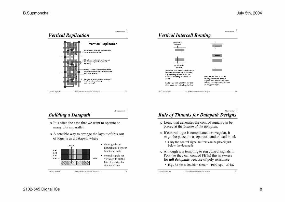
Replicating Cells
q What does this cell do?
q What if we want toreplicate this cellvertically, i.e., make astack of cells to processmany bits in parallel?ß Which nodes are shared
among the cells?
ß Which nodes are notshared?
ß How should we arrangethe cell vertically?
B.Supmonchai July 5th, 2004
2102-545 Digital ICs 8
2102-545 Digital ICs Design Rules and Layout Techniques 29
B.Supmonchai
Vertical Replication
2102-545 Digital ICs Design Rules and Layout Techniques 30
B.Supmonchai
Vertical Intercell Routing
2102-545 Digital ICs Design Rules and Layout Techniques 31
B.Supmonchai
Building a Datapath
q It is often the case that we want to operate onmany bits in parallel.
q A sensible way to arrange the layout of this sortof logic is as a datapath where
ß data signals runhorizontally betweenfunctional units
ß control signals runvertically to all thebits of a particularfunctional unit
2102-545 Digital ICs Design Rules and Layout Techniques 32
B.Supmonchai
Rule of Thumbs for Datapath Designs
q Logic that generates the control signals can beplaced at the bottom of the datapath.
q If control logic is complicated or irregular, itmight be placed in a separate standard cell blockß Only the control signal buffers can be placed just
below the data path
q Although it is tempting to run control signals inPoly (so they can control FETs) this is unwisefor tall datapaths because of poly resistanceß E.g., 32 bits x 20u/bit = 640u = ~1000 sqs. ~ 20 kΩ
B.Supmonchai July 5th, 2004
2102-545 Digital ICs 9
2102-545 Digital ICs Design Rules and Layout Techniques 33
B.Supmonchai
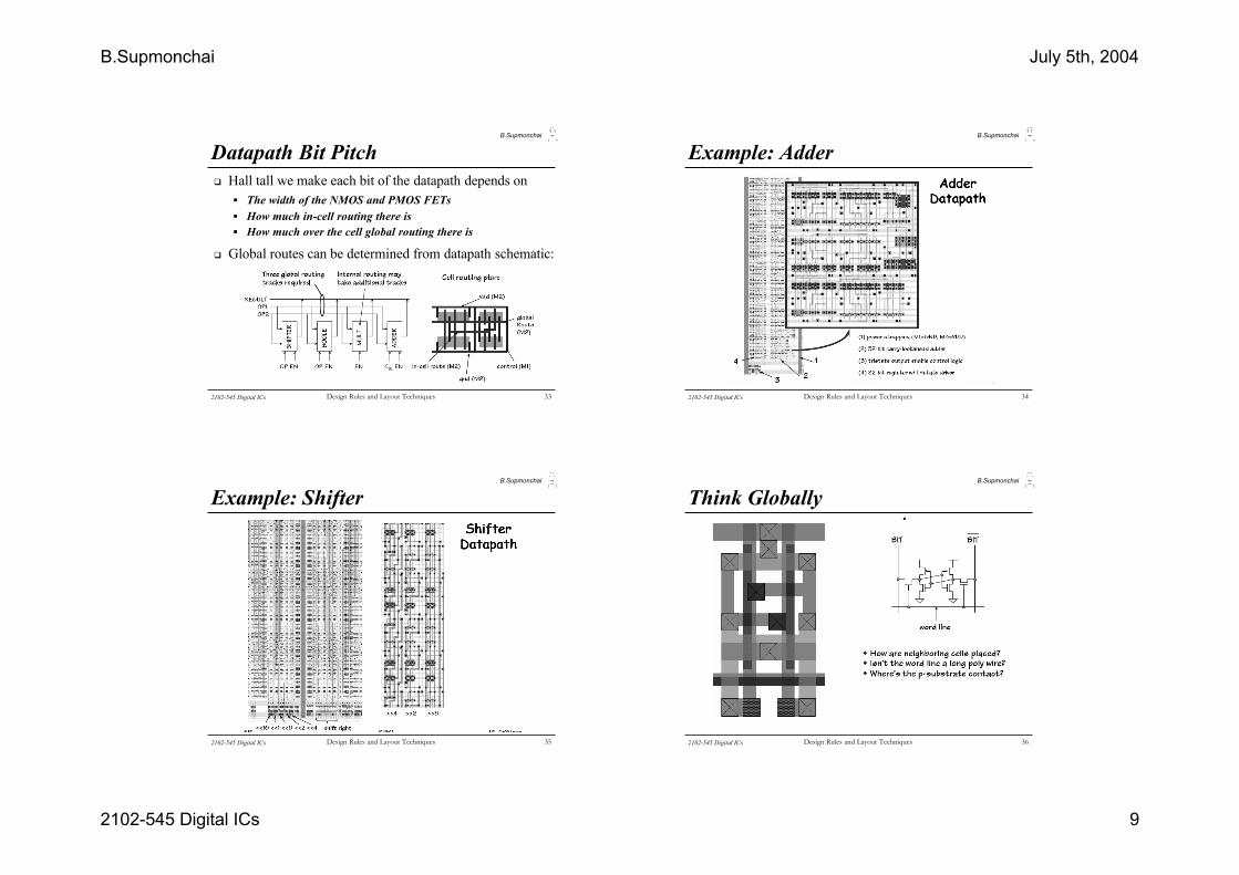
Datapath Bit Pitchq Hall tall we make each bit of the datapath depends onß The width of the NMOS and PMOS FETsß How much in-cell routing there isß How much over the cell global routing there is
q Global routes can be determined from datapath schematic:
2102-545 Digital ICs Design Rules and Layout Techniques 34
B.Supmonchai
Example: Adder
2102-545 Digital ICs Design Rules and Layout Techniques 35
B.Supmonchai
Example: Shifter
2102-545 Digital ICs Design Rules and Layout Techniques 36
B.Supmonchai
Think Globally

B.Supmonchai July 5th, 2004
2102-545 Digital ICs 10
2102-545 Digital ICs Design Rules and Layout Techniques 37
B.Supmonchai
Verifying the Layout
q Make sure that all the design rules are notviolated
q Verification of the Layout usually takes a verylong time.
ß Old timers use room-size layout plots.
ß Newbies use computer-aided design tools.ÿ Design Rule Checkers (DRC)
ÿ Layout vs Schematic (LVS)
2102-545 Digital ICs Design Rules and Layout Techniques 38
B.Supmonchai
Design Rule Checker (DRC)
q A program that checks each piece of the layoutagainst the process design rulesß Canonicalize layout into a set of leading and trailing
non-overlapping mask edges. Some boolean maskoperations may be needed.
ß Determine electrical connectivity and label eachedge with the node it belongs to.
ß Test each edge end point against neighboring edgesto check for spacing (leading edges) and width(trailing edges) violations.
q Computationally Intensive - A slow process!
2102-545 Digital ICs Design Rules and Layout Techniques 39
B.Supmonchai
Circuit Extraction
q Circuit Extractor derives a circuit schematicfrom a physical layout
ß Scan various layers and their interactions.
ß Reconstruct the transistor network, topologically
ß Generate a netlist file which describes all theinterconnection in the network.
q The netlist file contains precise information onthe parasitics
ß diffusion and wiring capacitances and resistance
2102-545 Digital ICs Design Rules and Layout Techniques 40
B.Supmonchai
Layout vs Schmetic (LVS)
q First a netlist is extracted from the layout.
q Use the electrical info generated by the DRCand then recognize which transistors arejuxtapositions of channel with diffusion
q See if extracted netlist is isomorphic to theschematic netlistß Initialize all nodes to the same color
ß Compute a new color for each node as some hashingfunction involving the colored node in other network
ß Worry about parallel FETs, ambiguous nodes