bs86c08c/bs86d12c bs86e16c/bs86d20c · 2018-11-07 · rev. 1.10 8 october 09, 2018 rev. 1.10 9...
TRANSCRIPT

Touch A/D Flash MCU with LED Driver
BS86C08C/BS86D12CBS86E16C/BS86D20C
Revision: V1.10 Date: October 09, 2018
Rev. 1.10 2 October 09, 2018 Rev. 1.10 3 October 09, 2018
BS86C08C/BS86D12CBS86E16C/BS86D20C
Touch A/D Flash MCU with LED Driver
BS86C08C/BS86D12CBS86E16C/BS86D20CTouch A/D Flash MCU with LED Driver
Table of Contents
Features ................................................................................................................ 7CPU Features ..............................................................................................................................7Peripheral Features ......................................................................................................................7
General Description ............................................................................................. 8Selection Table ..................................................................................................... 8Block Diagram ...................................................................................................... 9Pin Assignment .................................................................................................... 9Pin Descriptions ................................................................................................ 13Absolute Maximum Ratings .............................................................................. 23D.C. Electrical Characteristics .......................................................................... 23
Operating Voltage Characteristics ..............................................................................................23Operating Current Characteristics ..............................................................................................24Standby Current Characteristics ................................................................................................25
A.C. Characteristics ........................................................................................... 26High Speed Internal Oscillator – HIRC – Frequency Accuracy ..................................................26Low Speed Oscillators Characteristics – LIRC & LXT ...............................................................26Operating Frequency Characteristic Curves ..............................................................................27System Start Up Time Characteristics .......................................................................................27
Input/Output Characteristics ............................................................................ 28Memory Characteristics .................................................................................... 29LVD/LVR Electrical Characteristics .................................................................. 29A/D Converter Electrical Characteristics ......................................................... 30Internal Reference Voltage Characteristics ..................................................... 30Power-on Reset Characteristics ....................................................................... 30System Architecture .......................................................................................... 31
Clocking and Pipelining ..............................................................................................................31Program Counter ........................................................................................................................32Stack ..........................................................................................................................................32Arithmetic and Logic Unit – ALU ................................................................................................33
Flash Program Memory ..................................................................................... 34Structure .....................................................................................................................................34Special Vectors ..........................................................................................................................34Look-up Table .............................................................................................................................34Table Program Example .............................................................................................................35In Circuit Programming – ICP ....................................................................................................36On-Chip Debug Support – OCDS ..............................................................................................37
Data Memory ...................................................................................................... 38Structure ....................................................................................................................................38

Rev. 1.10 2 October 09, 2018 Rev. 1.10 3 October 09, 2018
BS86C08C/BS86D12CBS86E16C/BS86D20C
Touch A/D Flash MCU with LED Driver
BS86C08C/BS86D12CBS86E16C/BS86D20CTouch A/D Flash MCU with LED Driver
Data Memory Addressing ...........................................................................................................39General Purpose Data Memory .................................................................................................39Special Purpose Data Memory ..................................................................................................39
Special Function Register Description ............................................................ 44Indirect Addressing Registers – IAR0, IAR1, IAR2 ....................................................................44Memory Pointers – MP0, MP1L, MP1H, MP2L, MP2H ..............................................................44Program Memory Bank Pointer – PBP .......................................................................................45Accumulator – ACC ...................................................................................................................46Program Counter Low Register – PCL ......................................................................................46Look-up Table Registers – TBLP, TBHP, TBLH .........................................................................46Status Register – STATUS ........................................................................................................46
EEPROM Data Memory ...................................................................................... 48EEPROM Data Memory Structure .............................................................................................48EEPROM Registers ...................................................................................................................48Reading Data from the EEPROM ..............................................................................................50Writing Data to the EEPROM .....................................................................................................50Write Protection ..........................................................................................................................51EEPROM Interrupt .....................................................................................................................51Programming Considerations .....................................................................................................51
Oscillators .......................................................................................................... 52Oscillator Overview ....................................................................................................................52System Clock Configurations .....................................................................................................52Internal High Speed RC Oscillator – HIRC ................................................................................53Internal 32kHz Oscillator – LIRC ................................................................................................53External 32.768kHz Crystal Oscillator – LXT (BS86E16C/BS86D20C) .....................................53
Operating Modes and System Clocks ............................................................. 55System Clocks ...........................................................................................................................55System Operation Modes ...........................................................................................................56Control Registers .......................................................................................................................57Operating Mode Switching .........................................................................................................60Standby Current Considerations ................................................................................................62Wake-up .....................................................................................................................................63Programming Considerations .....................................................................................................63
Watchdog Timer ................................................................................................. 64Watchdog Timer Clock Source ...................................................................................................64Watchdog Timer Control Register ..............................................................................................64Watchdog Timer Operation ........................................................................................................65
Reset and Initialisation ...................................................................................... 66Reset Functions .........................................................................................................................66Reset Initial Conditions ..............................................................................................................69
Input/Output Ports ............................................................................................. 74Pull-high Resistors .....................................................................................................................75Port A Wake-up ..........................................................................................................................75

Rev. 1.10 4 October 09, 2018 Rev. 1.10 5 October 09, 2018
BS86C08C/BS86D12CBS86E16C/BS86D20C
Touch A/D Flash MCU with LED Driver
BS86C08C/BS86D12CBS86E16C/BS86D20CTouch A/D Flash MCU with LED Driver
I/O Port Control Registers ..........................................................................................................76I/O Port Source Current Selection ..............................................................................................76I/O Port Sink Current Selection ..................................................................................................79I/O Port Power Source Control – BS86E16C Only ....................................................................83Pin-remapping Function .............................................................................................................83I/O Pin Structures .......................................................................................................................87Programming Considerations .....................................................................................................88
Timer Modules – TM .......................................................................................... 89Introduction ................................................................................................................................89TM Operation .............................................................................................................................89TM Clock Source ........................................................................................................................89TM Interrupts ..............................................................................................................................90TM External Pins ........................................................................................................................90TM Input/Output Pin Control Register ........................................................................................90Programming Considerations .....................................................................................................94
Compact Type TM – CTM .................................................................................. 96Compact Type TM Operation .....................................................................................................96Compact Type TM Register Description.....................................................................................96Compact Type TM Operation Modes .......................................................................................101
Periodic Type TM – PTM .................................................................................. 107Periodic TM Operation .............................................................................................................107Periodic Type TM Register Description ....................................................................................107Periodic Type TM Operation Modes ......................................................................................... 112
Analog to Digital Converter ............................................................................ 121A/D Overview ...........................................................................................................................121A/D Converter Register Description .........................................................................................121A/D Converter Reference Voltage ............................................................................................125A/D Converter Input Signals .....................................................................................................125A/D Converter Operation ..........................................................................................................126Conversion Rate and Timing Diagram .....................................................................................127Summary of A/D Conversion Steps ..........................................................................................128Programming Considerations ...................................................................................................128A/D Transfer Function ..............................................................................................................129A/D Programming Examples ....................................................................................................129
Touch Key Function ........................................................................................ 131Touch Key Structure .................................................................................................................131Touch Key Register Definition ..................................................................................................132Touch Key Operation ................................................................................................................137Touch Key Interrupt ..................................................................................................................138Programming Considerations ...................................................................................................138
I2C Interface – BS86C08C/BS86D12C/BS86E16C .......................................... 139I2C Interface Operation .............................................................................................................139I2C Registers ............................................................................................................................140
Rev. 1.10 4 October 09, 2018 Rev. 1.10 5 October 09, 2018
BS86C08C/BS86D12CBS86E16C/BS86D20C
Touch A/D Flash MCU with LED Driver
BS86C08C/BS86D12CBS86E16C/BS86D20CTouch A/D Flash MCU with LED Driver
I2C Bus Communication ...........................................................................................................143I2C Time-out Control .................................................................................................................146
Serial Interface Module – SIM – BS86D20C ................................................... 148SPI Interface ............................................................................................................................148I2C Interface .............................................................................................................................157
UART Interfaces ............................................................................................... 166UARTn External Pins ...............................................................................................................167UARTn Data Transfer Scheme ................................................................................................167UARTn Status and Control Registers ......................................................................................167Baud Rate Generator ...............................................................................................................173UARTn Setup and Control .......................................................................................................173UARTn Transmitter ..................................................................................................................175UARTn Receiver ......................................................................................................................176Managing Receiver Errors .......................................................................................................177UARTn Interrupt Structure .......................................................................................................178UARTn Power Down and Wake-up ..........................................................................................180
Low Voltage Detector – LVD ........................................................................... 181LVD Register ............................................................................................................................181LVD Operation ..........................................................................................................................182
Interrupts .......................................................................................................... 183Interrupt Registers ....................................................................................................................183Interrupt Operation ...................................................................................................................189External Interrupt ......................................................................................................................192Touch Key Module Interrupt .....................................................................................................193Time Base Interrupts ................................................................................................................193I2C Interrupt – BS86C08C/BS86D12C/BS86E16C ..................................................................195Serial Interface Module Interrupt – BS86D20C ........................................................................195EEPROM Interrupt ...................................................................................................................196UART Transfer Interrupts .........................................................................................................196LVD Interrupt ............................................................................................................................196A/D Converter Interrupt ............................................................................................................196Multi-function Interrupt – BS86E16C/BS86D20C .....................................................................196TM Interrupts ............................................................................................................................197Interrupt Wake-up Function ......................................................................................................197Programming Considerations ...................................................................................................197
Configuration Options ..................................................................................... 198Application Circuits ......................................................................................... 199Instruction Set .................................................................................................. 200
Introduction ..............................................................................................................................200Instruction Timing .....................................................................................................................200Moving and Transferring Data ..................................................................................................200Arithmetic Operations ...............................................................................................................200Logical and Rotate Operation ..................................................................................................201

Rev. 1.10 6 October 09, 2018 Rev. 1.10 7 October 09, 2018
BS86C08C/BS86D12CBS86E16C/BS86D20C
Touch A/D Flash MCU with LED Driver
BS86C08C/BS86D12CBS86E16C/BS86D20CTouch A/D Flash MCU with LED Driver
Branches and Control Transfer ................................................................................................201Bit Operations ..........................................................................................................................201Table Read Operations ............................................................................................................201Other Operations ......................................................................................................................201
Instruction Set Summary ................................................................................ 202Table Conventions ....................................................................................................................202Extended Instruction Set ..........................................................................................................204
Instruction Definition ....................................................................................... 206Extended Instruction Definition ................................................................................................215
Package Information ....................................................................................... 22224-pin SOP (300mil) Outline Dimensions ................................................................................22324-pin SSOP (150mil) Outline Dimensions ..............................................................................22428-pin SOP (300mil) Outline Dimensions ................................................................................22528-pin SSOP (150mil) Outline Dimensions ..............................................................................22644-pin LQFP (10mm×10mm) (FP2.0mm) Outline Dimensions ................................................227

Rev. 1.10 6 October 09, 2018 Rev. 1.10 7 October 09, 2018
BS86C08C/BS86D12CBS86E16C/BS86D20C
Touch A/D Flash MCU with LED Driver
BS86C08C/BS86D12CBS86E16C/BS86D20CTouch A/D Flash MCU with LED Driver
Features
CPU Features• Operating Voltage:
♦ fSYS=8MHz: 2.2V~5.5V ♦ fSYS=12MHz: 2.7V~5.5V ♦ fSYS=16MHz: 3.3V~5.5V
• Up to 0.25μs instruction cycle with 16MHz system clock at VDD=5V
• Power down and wake-up functions to reduce power consumption
• Oscillator types: ♦ Internal High Speed 8/12/16MHz RC – HIRC ♦ Internal Low Speed 32kHz RC – LIRC ♦ External Low Speed 32.768kHz Crystal – LXT, for BS86E16C/BS86D20C
• Multi-mode operation: FAST, SLOW, IDLE and SLEEP
• Fully integrated internal oscillators require no external components
• All instructions executed in 1~3 instruction cycles
• Table read instructions
• 115 powerful instructions
• 8-level subroutine nesting
• Bit manipulation instruction
Peripheral Features• Flash Program Memory: 4K×16~16K×16
• Data Memory: 384×8~768×8
• True EEPROM Memory: 32×8~64×8
• Up to 20 touch key functions – fully integrated without requiring external components
• Watchdog Timer function
• Up to 42 bidirectional I/O lines
• Programmable I/O port source current and sink current for LED driver
• Single external interrupt line shared with I/O pin
• Multiple Timer Modules for time measurement, input capture, compare match output or PWM output or single pulse output function
• Up to 2 Time-Base functions for generation of fixed time interrupt signals
• 8-external-channel 12-bit resolution A/D converter
• I2C interface, for BS86C08C/BS86D12C/BS86E16C
• Serial Interface Module – SIM includes SPI and I2C interfaces, for BS86D20C only
• Up to 2 fully-duplex Universal Asynchronous Receiver and Transmitter Interfaces – UART
• Low voltage reset function
• Low voltage detect function
• Wide range of available package types

Rev. 1.10 8 October 09, 2018 Rev. 1.10 9 October 09, 2018
BS86C08C/BS86D12CBS86E16C/BS86D20C
Touch A/D Flash MCU with LED Driver
BS86C08C/BS86D12CBS86E16C/BS86D20CTouch A/D Flash MCU with LED Driver
General DescriptionThe series of devices are Flash Memory type 8-bit high performance RISC architecture microcontrollers with fully integrated touch key functions. With all touch key functions provided internally and with the convenience of Flash Memory multi-programming features, each device has all the features to offer designers a reliable and easy means of implementing Touch Keyes within their products applications.
The touch key functions are fully integrated completely eliminating the need for external components. In addition to the flash program memory, other memory includes an area of RAM Data Memory as well as an area of true EEPROM memory for storage of non-volatile data such as serial numbers, calibration data etc. Analog feature includes a multi-channel 12-bit A/D converter. Protective features such as an internal Watchdog Timer, Low Voltage Reset and Low Voltage Detector coupled with excellent noise immunity and ESD protection ensure that reliable operation is maintained in hostile electrical environments.
A full choice of external low, internal high and low speed oscillators are provided including fully integrated system oscillators which require no external components for its implementation. The ability to operate and switch dynamically between a range of operating modes using different clock sources gives users the ability to optimise microcontroller operation and minimise power consumption. Easy communication with the outside world is provided using the internal I2C, SPI and UART interfaces, while the inclusion of flexible I/O programming features, Time-Base functions, Timer Modules and many other features further enhance device functionality and flexibility.
The touch key devices will find excellent use in a huge range of modern Touch Key product applications such as sensor signal processing, home appliance, health care product, industrial control, consumer products, subsystem controllers to name but a few.
Selection TableMost features are common to all devices and the main features distinguishing them are Memory capacity, I/O count, Touch key count, UART, LXT, Time Base, Timer Module number and package types. The following table summarises the main features of each device.
Part No. Program Memory
Data Memory
Data EEPROM I/O External
Interrupt A/D Time Base
BS86C08C 4K×16 384×8 32×8 26 1 12-bit×8 1BS86D12C 8K×16 512×8 64×8 26 1 12-bit×8 1BS86E16C 16K×16 768×8 64×8 42 1 12-bit×8 2BS86D20C 8K×16 768×8 64×8 26 1 12-bit×8 2
Part No. Timer Module Touch Key I2C SIM(SPI+I2C) UART LXT Stack Package
BS86C08C 10-bit CTM×110-bit PTM×1 8 √ — 1 — 8 24SOP/SSOP
28SOP/SSOP
BS86D12C 10-bit CTM×110-bit PTM×1 12 √ — 1 — 8 24SOP/SSOP
28SOP/SSOP
BS86E16C 10-bit CTM×110-bit PTM×2 16 √ — 2 √ 8 28SOP/SSOP
44LQFP
BS86D20C 10-bit CTM×110-bit PTM×2 20 — √ 1 √ 8 24/28SOP
Note: As devices exist in more than one package format, the table reflects the situation for the package with the most pins.

Rev. 1.10 8 October 09, 2018 Rev. 1.10 9 October 09, 2018
BS86C08C/BS86D12CBS86E16C/BS86D20C
Touch A/D Flash MCU with LED Driver
BS86C08C/BS86D12CBS86E16C/BS86D20CTouch A/D Flash MCU with LED Driver
Block Diagram
Bus
MUX
Stack8-level
RAM768 × 8
ROM16K × 16
WatchdogTimer
LIRC32kHz
LXT
Clock System
HT8 MCU Core
Time Bases
EEPROM64 × 8
LVR/LVD
XT1XT2
HIRC8/12/16MHz
Pin-SharedWith Port A or D
Interrupt ControllerINT
Pin-SharedWith Port A
Reset Circuit
VDD
MU
X
AN0~AN7
Pin-SharedWith Port C or D
VREF
VBG
Analog to Digital Converter
VSS
VDD VDD
VSS
Pin-SharedWith Port D
: SIM including SPI & I2C: Bus Entry : Pin-Shared Node
12-bit ADC
VDDIO VDDIO
Analog Peripherals
MUXBS86E16C/D20C
BS86E16C
Timers
Digital Peripherals
I/O
UART
Port ADriver
Pin-Remapping Function
PA0~PA4, PA7
PB0~PB7
PD0~PD7
Port BDriver
Port DDriver
PC0~PC7Port CDriver
PE0~PE7Port EDriver
PF0~PF3Port FDriver
I2C
BS86C08C/D12C/E16C
BS86D20C
SIM
Touch Key Module 4
Touch Key Module 1
Pin-SharedWith Port A, B & C
KEY1~KEY20
Touch Key Function
Touch Key Module 0
MU
XC to F Circuit
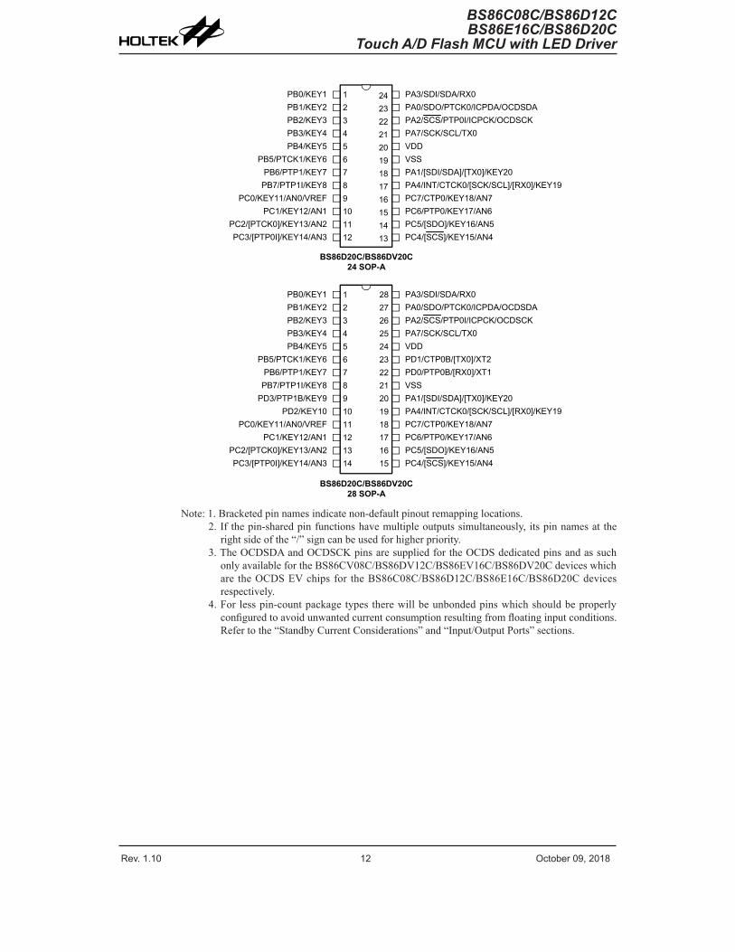
Pin Assignment
BS86C08C/BS86CV08C24 SOP-A/SSOP-A
242322212019181716151413
123456789101112
PB0/KEY1 PA7/PTCK0/CTCK0PB1/KEY2 PA4/PTP0I/CTP0/INTPB2/KEY3 PA2/PTP0B/ICPCK/OCDSCKPB3/KEY4 PA0/CTP0B/ICPDA/OCDSDAPB4/KEY5 VDD
PC0/[CTCK0]
PA3/[SDA]/TX0PB5/KEY6PA1/[SCL]/RX0
PB7/KEY8 VSSPB6/KEY7
PD5/PTP0/AN5PC1/[CTP0] PD4/AN4/VREF
PC2/[SCL]/[RX0] PD3/AN3PC3/[SDA]/[TX0] PD2/AN2

Rev. 1.10 10 October 09, 2018 Rev. 1.10 11 October 09, 2018
BS86C08C/BS86D12CBS86E16C/BS86D20C
Touch A/D Flash MCU with LED Driver
BS86C08C/BS86D12CBS86E16C/BS86D20CTouch A/D Flash MCU with LED Driver
BS86C08C/BS86CV08C28 SOP-A/SSOP-A
PB2/KEY3
PD2/AN2PD3/AN3PD4/AN4/VREF
VDD
VSS
PA2/PTP0B/ICPCK/OCDSCK
PA7/PTCK0/CTCK0
PD6/SCL/[RX0]/AN6PD7/SDA/[TX0]/AN7
PD5/PTP0/AN5PD1/AN1PD0/AN0
PB4/KEY5PB5/KEY6PB6/KEY7PB7/KEY8
PC1/[CTP0]PC0/[CTCK0]
PC2/[SCL]/[RX0]PC3/[SDA]/[TX0]
2827262524232221201918171615
1234567891011121314
PB3/KEY4
PB1/KEY2PB0/KEY1
PA4/PTP0I/CTP0/INT
PA0/CTP0B/ICPDA/OCDSDA
PA3/[SDA]/TX0PA1/[SCL]/RX0
BS86D12C/BS86DV12C24 SOP-A/SSOP-A
242322212019181716151413
123456789101112
PB0/KEY1 PA7/PTCK0/CTCK0PB1/KEY2 PA4/PTP0I/CTP0/INTPB2/KEY3 PA2/PTP0B/ICPCK/OCDSCKPB3/KEY4 PA0/CTP0B/ICPDA/OCDSDAPB4/KEY5 VDD
PC0/[CTCK0]/KEY9
PA3/[SDA]/TX0PB5/KEY6PA1/[SCL]/RX0
PB7/KEY8 VSSPB6/KEY7
PD5/PTP0/AN5PC1/[CTP0]/KEY10 PD4/AN4/VREF
PC2/[SCL]/[RX0]/KEY11 PD3/AN3PC3/[SDA]/[TX0]/KEY12 PD2/AN2
BS86D12C/BS86DV12C28 SOP-A/SSOP-A
PB2/KEY3
PD2/AN2PD3/AN3PD4/AN4/VREF
VDD
VSS
PA2/PTP0B/ICPCK/OCDSCK
PA7/PTCK0/CTCK0
PD6/SCL/[RX0]/AN6PD7/SDA/[TX0]/AN7
PD5/PTP0/AN5PD1/AN1PD0/AN0
PB4/KEY5PB5/KEY6PB6/KEY7PB7/KEY8
PC1/[CTP0]/KEY10PC0/[CTCK0]/KEY9
PC2/[SCL]/[RX0]/KEY11PC3/[SDA]/[TX0]/KEY12
2827262524232221201918171615
1234567891011121314
PB3/KEY4
PB1/KEY2PB0/KEY1
PA4/PTP0I/CTP0/INT
PA0/CTP0B/ICPDA/OCDSDA
PA3/[SDA]/TX0PA1/[SCL]/RX0

Rev. 1.10 10 October 09, 2018 Rev. 1.10 11 October 09, 2018
BS86C08C/BS86D12CBS86E16C/BS86D20C
Touch A/D Flash MCU with LED Driver
BS86C08C/BS86D12CBS86E16C/BS86D20CTouch A/D Flash MCU with LED Driver
BS86E16C/BS86EV16C28 SOP-A/SSOP-A
PB2/KEY3
PD2/[PTP1I]/[RX1]/AN2PD3/[PTP1]/[TX1]/AN3PD4/[PTCK1]/AN4/VREF
VDD
VSS
PA2/PTP0B/ICPCK/OCDSCK
PA7/PTCK0/CTCK0/[TX1]
PD6/SCL/[RX0]/AN6PD7/SDA/[TX0]/AN7
PD5/[PTP0]/AN5PD1/AN1PD0/AN0
PB4/KEY5PB5/KEY6PB6/KEY7PB7/KEY8
PC1/[CTP0]/KEY10PC0/[CTCK0]/KEY9
PC2/[SCL]/[RX0]/KEY11PC3/[SDA]/[TX0]/KEY12
2827262524232221201918171615
1234567891011121314
PB3/KEY4
PB1/KEY2PB0/KEY1
PA4/PTP0I/CTP0/INT/[RX1]
PA0/[CTP0B]/ICPDA/OCDSDA
PA3/[SDA]/TX0/XT2PA1/[SCL]/RX0/XT1
PC
1/[CTP
0]/KE
Y10
PB4/KEY5PB5/KEY6PB6/KEY7PB7/KEY8
PC
0/[CTC
K0]/KE
Y9
PC
4/KEY
13P
C5/K
EY14
PC
6/[SC
L]/KE
Y15
PB
0/KE
Y1
PF0/[CTP0]/R
X1P
C7/[S
DA
]/KE
Y16
PD1/AN1
PD2/[PTP1I]/[R
X1]/AN2
PD
3/[PTP
1]/[TX1]/AN
3
PD0/AN0
VDD
PE7/PTCK1VSS
PB3/KEY4
PA0/[CTP0B]/IC
PDA/O
CD
SDA
PA4/PTP0I/CTP0/IN
T/[RX1]
PD
4/[PTC
K1]/AN
4/VR
EF
PD6/SCL/[RX0]/AN6PD7/SDA/[TX0]/AN7
PD5/[PTP0]/AN5
PC
2/[SC
L]/[RX0]/K
EY
11P
C3/[S
DA
]/[TX0]/KE
Y12
PE0/[RX0]PE1/[TX0]
PE3/[PTP1B]/[TX1]PE2/[RX1]
BS86E16C/BS86EV16C44 LQFP-B
1234567891011
12 13 14 15 16 17 18 19 20 21 222324252627282930313233
3435363738394041424344
PB
1/KE
Y2
PB
2/KE
Y3
PF1/[C
TCK
0]/TX1
PF2/C
TP0B
PF3/PTP
0
PA7/PTCK0/C
TCK0/[TX1]
PA2/PTP0B/ICPC
K/OC
DSC
K
PA3/[SDA]/TX0/XT2PA1/[SCL]/RX0/XT1
PE6/PTP1IPE5/PTP1BPE4/PTP1/VDDIO
Rev. 1.10 12 October 09, 2018 Rev. 1.10 13 October 09, 2018
BS86C08C/BS86D12CBS86E16C/BS86D20C
Touch A/D Flash MCU with LED Driver
BS86C08C/BS86D12CBS86E16C/BS86D20CTouch A/D Flash MCU with LED Driver
PB0/KEY1 PA3/SDI/SDA/RX0
BS86D20C/BS86DV20C24 SOP-A
PB1/KEY2PB2/KEY3PB3/KEY4PB4/KEY5
PB5/PTCK1/KEY6PB6/PTP1/KEY7PB7/PTP1I/KEY8
PC0/KEY11/AN0/VREFPC1/KEY12/AN1
PC2/[PTCK0]/KEY13/AN2PC3/[PTP0I]/KEY14/AN3
PA0/SDO/PTCK0/ICPDA/OCDSDAPA2/SCS/PTP0I/ICPCK/OCDSCKPA7/SCK/SCL/TX0VDDVSSPA1/[SDI/SDA]/[TX0]/KEY20PA4/INT/CTCK0/[SCK/SCL]/[RX0]/KEY19PC7/CTP0/KEY18/AN7PC6/PTP0/KEY17/AN6PC5/[SDO]/KEY16/AN5PC4/[SCS]/KEY15/AN4
242322212019181716151413
123456789101112
PB0/KEY1 PA3/SDI/SDA/RX0
BS86D20C/BS86DV20C28 SOP-A
2827262524232221201918171615
1234567891011121314
PB1/KEY2PB2/KEY3PB3/KEY4PB4/KEY5
PB5/PTCK1/KEY6PB6/PTP1/KEY7PB7/PTP1I/KEY8PD3/PTP1B/KEY9
PD2/KEY10PC0/KEY11/AN0/VREF
PC1/KEY12/AN1PC2/[PTCK0]/KEY13/AN2PC3/[PTP0I]/KEY14/AN3
PA0/SDO/PTCK0/ICPDA/OCDSDAPA2/SCS/PTP0I/ICPCK/OCDSCKPA7/SCK/SCL/TX0VDDPD1/CTP0B/[TX0]/XT2PD0/PTP0B/[RX0]/XT1VSSPA1/[SDI/SDA]/[TX0]/KEY20PA4/INT/CTCK0/[SCK/SCL]/[RX0]/KEY19PC7/CTP0/KEY18/AN7PC6/PTP0/KEY17/AN6PC5/[SDO]/KEY16/AN5PC4/[SCS]/KEY15/AN4
Note: 1. Bracketed pin names indicate non-default pinout remapping locations.2. If the pin-shared pin functions have multiple outputs simultaneously, its pin names at the
right side of the “/” sign can be used for higher priority. 3. The OCDSDA and OCDSCK pins are supplied for the OCDS dedicated pins and as such
only available for the BS86CV08C/BS86DV12C/BS86EV16C/BS86DV20C devices which are the OCDS EV chips for the BS86C08C/BS86D12C/BS86E16C/BS86D20C devices respectively.
4. For less pin-count package types there will be unbonded pins which should be properly configured to avoid unwanted current consumption resulting from floating input conditions. Refer to the “Standby Current Considerations” and “Input/Output Ports” sections.
Rev. 1.10 12 October 09, 2018 Rev. 1.10 13 October 09, 2018
BS86C08C/BS86D12CBS86E16C/BS86D20C
Touch A/D Flash MCU with LED Driver
BS86C08C/BS86D12CBS86E16C/BS86D20CTouch A/D Flash MCU with LED Driver
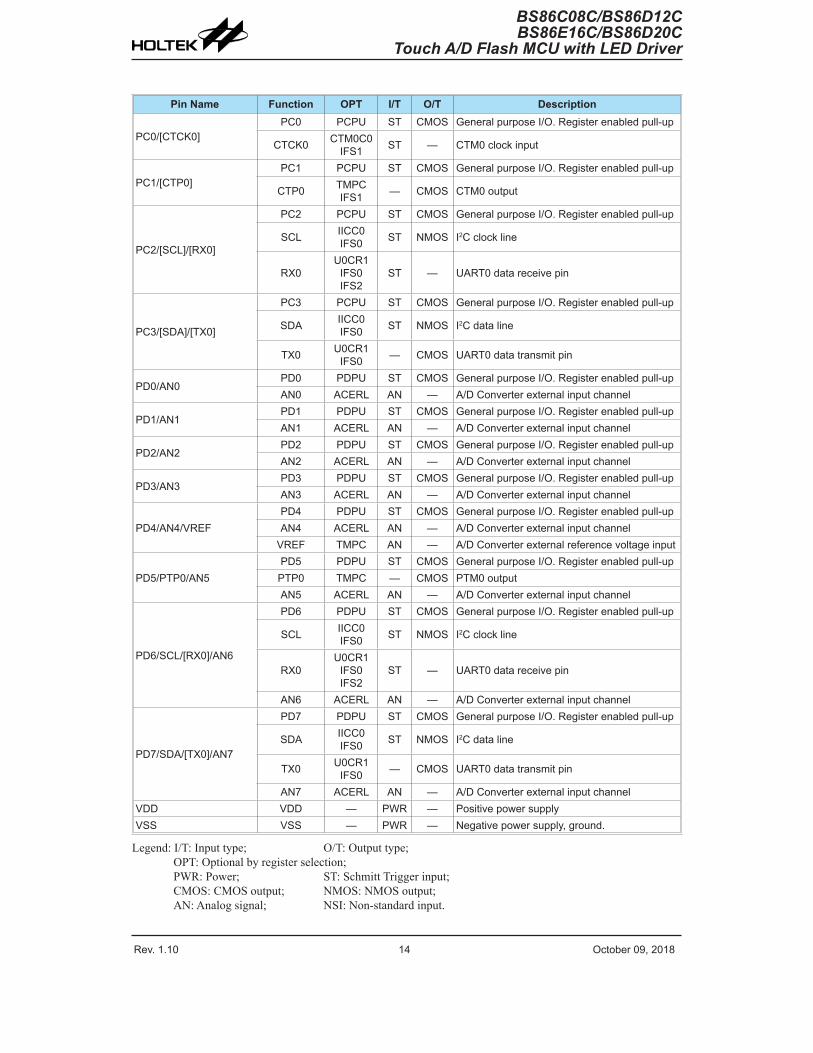
Pin DescriptionsWith the exception of the power pins, all pins on the devices can be referenced by their Port name, e.g. PA0, PA1 etc., which refer to the digital I/O function of the pins. However these Port pins are also shared with other function such as the Touch Key function, Timer Module pins etc. The function of each pin is listed in the following table, however the details behind how each pin is configured is contained in other sections of the datasheet.
As the Pin Description table shows the situation for the package with the most pins, not all pins in the table will be available on smaller package sizes.
BS86C08C/BS86CV08C
Pin Name Function OPT I/T O/T Description
PA0/CTP0B/ICPDA/OCDSDA
PA0 PAPUPAWU ST CMOS General purpose I/O. Register enabled pull-up
and wake-upCTP0B TMPC — CMOS CTM0 inverted outputICPDA — ST CMOS ICP data/address pin
OCDSDA — ST CMOS OCDS data/address pin, for EV chip only.
PA1/[SCL]/RX0
PA1 PAPUPAWU ST CMOS General purpose I/O. Register enabled pull-up
and wake-up
SCL IICC0IFS0 ST NMOS I2C clock line
RX0U0CR1
IFS0IFS2
ST — UART0 data receive pin
PA2/PTP0B/ICPCK/OCDSCK
PA2 PAPUPAWU ST CMOS General purpose I/O. Register enabled pull-up
and wake-upPTP0B TMPC — CMOS PTM0 inverted outputICPCK — ST — ICP clock pin
OCDSCK — ST — OCDS clock pin, for EV chip only
PA3/[SDA]/TX0
PA3 PAPUPAWU ST CMOS General purpose I/O. Register enabled pull-up
and wake-up
SDA IICC0IFS0 ST NMOS I2C data line
TX0 U0CR1IFS0 — CMOS UART0 data transmit pin
PA4/PTP0I/CTP0/INT
PA4 PAPUPAWU ST CMOS General purpose I/O. Register enabled pull-up
and wake-up
PTP0I PTM0C0PTM0C1 ST — PTM0 capture input
CTP0 TMPCIFS1 — CMOS CTM0 output
INT INTC0INTEG ST — External interrupt input
PA7/PTCK0/CTCK0
PA7 PAPUPAWU ST CMOS General purpose I/O. Register enabled pull-up
and wake-upPTCK0 PTM0C0 ST — PTM0 clock input
CTCK0 CTM0C0IFS1 ST — CTM0 clock input
PB0/KEY1~PB3/KEY4PB0~PB3 PBPU ST CMOS General purpose I/O. Register enabled pull-up
KEY1~KEY4 TKM0C1 NSI — Touch key input
PB4/KEY5~PB7/KEY8PB4~PB7 PBPU ST CMOS General purpose I/O. Register enabled pull-up
KEY5~KEY8 TKM1C1 NSI — Touch key input
Rev. 1.10 14 October 09, 2018 Rev. 1.10 15 October 09, 2018
BS86C08C/BS86D12CBS86E16C/BS86D20C
Touch A/D Flash MCU with LED Driver
BS86C08C/BS86D12CBS86E16C/BS86D20CTouch A/D Flash MCU with LED Driver
Pin Name Function OPT I/T O/T Description
PC0/[CTCK0]PC0 PCPU ST CMOS General purpose I/O. Register enabled pull-up
CTCK0 CTM0C0IFS1 ST — CTM0 clock input
PC1/[CTP0]PC1 PCPU ST CMOS General purpose I/O. Register enabled pull-up
CTP0 TMPCIFS1 — CMOS CTM0 output
PC2/[SCL]/[RX0]
PC2 PCPU ST CMOS General purpose I/O. Register enabled pull-up
SCL IICC0IFS0 ST NMOS I2C clock line
RX0U0CR1
IFS0IFS2
ST — UART0 data receive pin
PC3/[SDA]/[TX0]
PC3 PCPU ST CMOS General purpose I/O. Register enabled pull-up
SDA IICC0IFS0 ST NMOS I2C data line
TX0 U0CR1IFS0 — CMOS UART0 data transmit pin
PD0/AN0PD0 PDPU ST CMOS General purpose I/O. Register enabled pull-upAN0 ACERL AN — A/D Converter external input channel
PD1/AN1PD1 PDPU ST CMOS General purpose I/O. Register enabled pull-upAN1 ACERL AN — A/D Converter external input channel
PD2/AN2PD2 PDPU ST CMOS General purpose I/O. Register enabled pull-upAN2 ACERL AN — A/D Converter external input channel
PD3/AN3PD3 PDPU ST CMOS General purpose I/O. Register enabled pull-upAN3 ACERL AN — A/D Converter external input channel
PD4/AN4/VREFPD4 PDPU ST CMOS General purpose I/O. Register enabled pull-upAN4 ACERL AN — A/D Converter external input channel
VREF TMPC AN — A/D Converter external reference voltage input
PD5/PTP0/AN5PD5 PDPU ST CMOS General purpose I/O. Register enabled pull-upPTP0 TMPC — CMOS PTM0 outputAN5 ACERL AN — A/D Converter external input channel
PD6/SCL/[RX0]/AN6
PD6 PDPU ST CMOS General purpose I/O. Register enabled pull-up
SCL IICC0IFS0 ST NMOS I2C clock line
RX0U0CR1
IFS0IFS2
ST — UART0 data receive pin
AN6 ACERL AN — A/D Converter external input channel
PD7/SDA/[TX0]/AN7
PD7 PDPU ST CMOS General purpose I/O. Register enabled pull-up
SDA IICC0IFS0 ST NMOS I2C data line
TX0 U0CR1IFS0 — CMOS UART0 data transmit pin
AN7 ACERL AN — A/D Converter external input channelVDD VDD — PWR — Positive power supplyVSS VSS — PWR — Negative power supply, ground.
Legend: I/T: Input type; O/T: Output type;OPT: Optional by register selection;PWR: Power; ST: Schmitt Trigger input;CMOS: CMOS output; NMOS: NMOS output;AN: Analog signal; NSI: Non-standard input.
Rev. 1.10 14 October 09, 2018 Rev. 1.10 15 October 09, 2018
BS86C08C/BS86D12CBS86E16C/BS86D20C
Touch A/D Flash MCU with LED Driver
BS86C08C/BS86D12CBS86E16C/BS86D20CTouch A/D Flash MCU with LED Driver
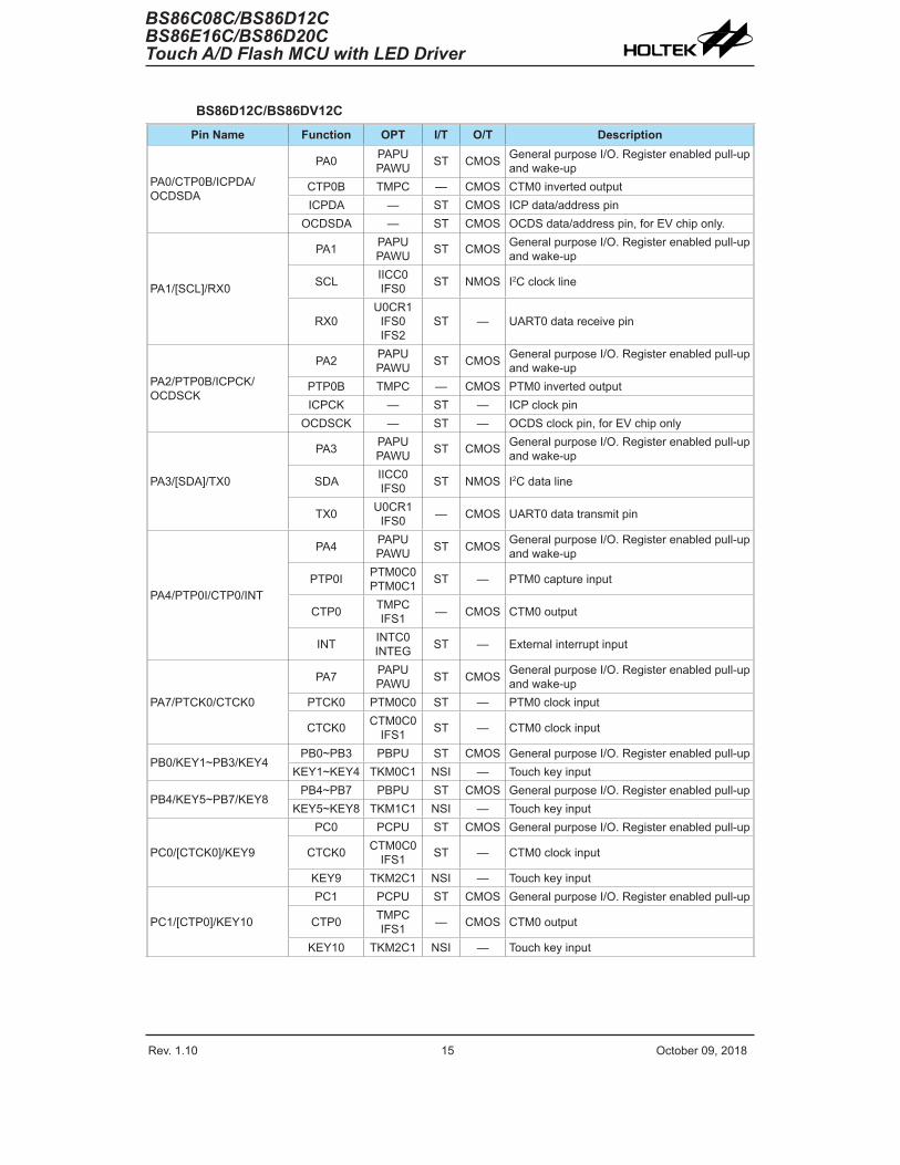
BS86D12C/BS86DV12C
Pin Name Function OPT I/T O/T Description
PA0/CTP0B/ICPDA/OCDSDA
PA0 PAPUPAWU ST CMOS General purpose I/O. Register enabled pull-up
and wake-upCTP0B TMPC — CMOS CTM0 inverted outputICPDA — ST CMOS ICP data/address pin
OCDSDA — ST CMOS OCDS data/address pin, for EV chip only.
PA1/[SCL]/RX0
PA1 PAPUPAWU ST CMOS General purpose I/O. Register enabled pull-up
and wake-up
SCL IICC0IFS0 ST NMOS I2C clock line
RX0U0CR1
IFS0IFS2
ST — UART0 data receive pin
PA2/PTP0B/ICPCK/OCDSCK
PA2 PAPUPAWU ST CMOS General purpose I/O. Register enabled pull-up
and wake-upPTP0B TMPC — CMOS PTM0 inverted outputICPCK — ST — ICP clock pin
OCDSCK — ST — OCDS clock pin, for EV chip only
PA3/[SDA]/TX0
PA3 PAPUPAWU ST CMOS General purpose I/O. Register enabled pull-up
and wake-up
SDA IICC0IFS0 ST NMOS I2C data line
TX0 U0CR1IFS0 — CMOS UART0 data transmit pin
PA4/PTP0I/CTP0/INT
PA4 PAPUPAWU ST CMOS General purpose I/O. Register enabled pull-up
and wake-up
PTP0I PTM0C0PTM0C1 ST — PTM0 capture input
CTP0 TMPCIFS1 — CMOS CTM0 output
INT INTC0INTEG ST — External interrupt input
PA7/PTCK0/CTCK0
PA7 PAPUPAWU ST CMOS General purpose I/O. Register enabled pull-up
and wake-upPTCK0 PTM0C0 ST — PTM0 clock input
CTCK0 CTM0C0IFS1 ST — CTM0 clock input
PB0/KEY1~PB3/KEY4PB0~PB3 PBPU ST CMOS General purpose I/O. Register enabled pull-up
KEY1~KEY4 TKM0C1 NSI — Touch key input
PB4/KEY5~PB7/KEY8PB4~PB7 PBPU ST CMOS General purpose I/O. Register enabled pull-up
KEY5~KEY8 TKM1C1 NSI — Touch key input
PC0/[CTCK0]/KEY9
PC0 PCPU ST CMOS General purpose I/O. Register enabled pull-up
CTCK0 CTM0C0IFS1 ST — CTM0 clock input
KEY9 TKM2C1 NSI — Touch key input
PC1/[CTP0]/KEY10
PC1 PCPU ST CMOS General purpose I/O. Register enabled pull-up
CTP0 TMPCIFS1 — CMOS CTM0 output
KEY10 TKM2C1 NSI — Touch key input

Rev. 1.10 16 October 09, 2018 Rev. 1.10 17 October 09, 2018
BS86C08C/BS86D12CBS86E16C/BS86D20C
Touch A/D Flash MCU with LED Driver
BS86C08C/BS86D12CBS86E16C/BS86D20CTouch A/D Flash MCU with LED Driver
Pin Name Function OPT I/T O/T Description
PC2/[SCL]/[RX0]/KEY11
PC2 PCPU ST CMOS General purpose I/O. Register enabled pull-up
SCL IICC0IFS0 ST NMOS I2C clock line
RX0U0CR1
IFS0IFS2
ST — UART0 data receive pin
KEY11 TKM2C1 NSI — Touch key input
PC3/[SDA]/[TX0]/KEY12
PC3 PCPU ST CMOS General purpose I/O. Register enabled pull-up
SDA IICC0IFS0 ST NMOS I2C data line
TX0 U0CR1IFS0 — CMOS UART0 data transmit pin
KEY12 TKM2C1 NSI — Touch key input
PD0/AN0PD0 PDPU ST CMOS General purpose I/O. Register enabled pull-upAN0 ACERL AN — A/D Converter external input channel
PD1/AN1PD1 PDPU ST CMOS General purpose I/O. Register enabled pull-upAN1 ACERL AN — A/D Converter external input channel
PD2/AN2PD2 PDPU ST CMOS General purpose I/O. Register enabled pull-upAN2 ACERL AN — A/D Converter external input channel
PD3/AN3PD3 PDPU ST CMOS General purpose I/O. Register enabled pull-upAN3 ACERL AN — A/D Converter external input channel
PD4/AN4/VREFPD4 PDPU ST CMOS General purpose I/O. Register enabled pull-upAN4 ACERL AN — A/D Converter external input channel
VREF TMPC AN — A/D Converter external reference voltage input
PD5/PTP0/AN5PD5 PDPU ST CMOS General purpose I/O. Register enabled pull-upPTP0 TMPC — CMOS PTM0 outputAN5 ACERL AN — A/D Converter external input channel
PD6/SCL/[RX0]/AN6
PD6 PDPU ST CMOS General purpose I/O. Register enabled pull-up
SCL IICC0IFS0 ST NMOS I2C clock line
RX0U0CR1
IFS0IFS2
ST — UART0 data receive pin
AN6 ACERL AN — A/D Converter external input channel
PD7/SDA/[TX0]/AN7
PD7 PDPU ST CMOS General purpose I/O. Register enabled pull-up
SDA IICC0IFS0 ST NMOS I2C data line
TX0 U0CR1IFS0 — CMOS UART0 data transmit pin
AN7 ACERL AN — A/D Converter external input channelVDD VDD — PWR — Positive power supplyVSS VSS — PWR — Negative power supply, ground.
Legend: I/T: Input type; O/T: Output type;OPT: Optional by register selection;PWR: Power; ST: Schmitt Trigger input;CMOS: CMOS output; NMOS: NMOS output;AN: Analog signal; NSI: Non-standard input.

Rev. 1.10 16 October 09, 2018 Rev. 1.10 17 October 09, 2018
BS86C08C/BS86D12CBS86E16C/BS86D20C
Touch A/D Flash MCU with LED Driver
BS86C08C/BS86D12CBS86E16C/BS86D20CTouch A/D Flash MCU with LED Driver
BS86E16C/BS86EV16C
Pin Name Function OPT I/T O/T Description
PA0/[CTP0B]/ICPDA/OCDSDA
PA0 PAPUPAWU ST CMOS General purpose I/O. Register enabled pull-up
and wake-up
CTP0B TMPCIFS1 — CMOS CTM0 inverted output
ICPDA — ST CMOS ICP data/address pinOCDSDA — ST CMOS OCDS data/address pin, for EV chip only.
PA1/[SCL]/RX0/XT1
PA1 PAPUPAWU ST CMOS General purpose I/O. Register enabled pull-up
and wake-up
SCL IICC0IFS0 ST NMOS I2C clock line
RX0U0CR1
IFS0IFS2
ST — UART0 data receive pin
XT1 CO LXT — LXT oscillator pin
PA2/PTP0B/ICPCK/OCDSCK
PA2 PAPUPAWU ST CMOS General purpose I/O. Register enabled pull-up
and wake-upPTP0B TMPC — CMOS PTM0 inverted outputICPCK — ST — ICP clock pin
OCDSCK — ST — OCDS clock pin, for EV chip only
PA3/[SDA]/TX0/XT2
PA3 PAPUPAWU ST CMOS General purpose I/O. Register enabled pull-up
and wake-up
SDA IICC0IFS0 ST NMOS I2C data line
TX0 U0CR1IFS0 — CMOS UART0 data transmit pin
XT2 CO — LXT LXT oscillator pin
PA4/PTP0I/CTP0/INT/[RX1]
PA4 PAPUPAWU ST CMOS General purpose I/O. Register enabled pull-up
and wake-up
PTP0I PTM0C0PTM0C1 ST — PTM0 capture input
CTP0 TMPCIFS1 — CMOS CTM0 output
INT INTC0INTEG ST — External interrupt input
RX1 U1CR1IFS2 ST — UART1 data receive pin
PA7/PTCK0/CTCK0/[TX1]
PA7 PAPUPAWU ST CMOS General purpose I/O. Register enabled pull-up
and wake-upPTCK0 PTM0C0 ST — PTM0 clock input
CTCK0 CTM0C0IFS1 ST — CTM0 clock input
TX1 U1CR1IFS2 — CMOS UART1 data transmit pin
PB0/KEY1~PB3/KEY4PB0~PB3 PBPU ST CMOS General purpose I/O. Register enabled pull-up
KEY1~KEY4 TKM0C1 NSI — Touch key input
PB4/KEY5~PB7/KEY8PB4~PB7 PBPU ST CMOS General purpose I/O. Register enabled pull-up
KEY5~KEY8 TKM1C1 NSI — Touch key input
PC0/[CTCK0]/KEY9
PC0 PCPU ST CMOS General purpose I/O. Register enabled pull-up
CTCK0 CTM0C0IFS1 ST — CTM0 clock input
KEY9 TKM2C1 NSI — Touch key input

Rev. 1.10 18 October 09, 2018 Rev. 1.10 19 October 09, 2018
BS86C08C/BS86D12CBS86E16C/BS86D20C
Touch A/D Flash MCU with LED Driver
BS86C08C/BS86D12CBS86E16C/BS86D20CTouch A/D Flash MCU with LED Driver
Pin Name Function OPT I/T O/T Description
PC1/[CTP0]/KEY10
PC1 PCPU ST CMOS General purpose I/O. Register enabled pull-up
CTP0 TMPCIFS1 — CMOS CTM0 output
KEY10 TKM2C1 NSI — Touch key input
PC2/[SCL]/[RX0]/KEY11
PC2 PCPU ST CMOS General purpose I/O. Register enabled pull-up
SCL IICC0IFS0 ST NMOS I2C clock line
RX0U0CR1
IFS0IFS2
ST — UART0 data receive pin
KEY11 TKM2C1 NSI — Touch key input
PC3/[SDA]/[TX0]/KEY12
PC3 PCPU ST CMOS General purpose I/O. Register enabled pull-up
SDA IICC0IFS0 ST NMOS I2C data line
TX0 U0CR1IFS0 — CMOS UART0 data transmit pin
KEY12 TKM2C1 NSI — Touch key input
PC4/KEY13PC4 PCPU ST CMOS General purpose I/O. Register enabled pull-up
KEY13 TKM3C1 NSI — Touch key input
PC5/KEY14PC5 PCPU ST CMOS General purpose I/O. Register enabled pull-up
KEY14 TKM3C1 NSI — Touch key input
PC6/[SCL]/KEY15
PC6 PCPU ST CMOS General purpose I/O. Register enabled pull-up
SCL IICC0IFS0 ST NMOS I2C clock line
KEY15 TKM3C1 NSI — Touch key input
PC7/[SDA]/KEY16
PC7 PCPU ST CMOS General purpose I/O. Register enabled pull-up
SDA IICC0IFS0 ST NMOS I2C data line
KEY16 TKM3C1 NSI — Touch key input
PD0/AN0PD0 PDPU ST CMOS General purpose I/O. Register enabled pull-upAN0 ACERL AN — A/D Converter external input channel
PD1/AN1PD1 PDPU ST CMOS General purpose I/O. Register enabled pull-upAN1 ACERL AN — A/D Converter external input channel
PD2/[PTP1I]/[RX1]/AN2
PD2 PDPU ST CMOS General purpose I/O. Register enabled pull-up
PTP1IPTM1C0PTM1C1
IFS1ST — PTM1 capture input
RX1 U1CR1IFS2 ST — UART1 data receive pin
AN2 ACERL AN — A/D Converter external input channel
PD3/[PTP1]/[TX1]/AN3
PD3 PDPU ST CMOS General purpose I/O. Register enabled pull-up
PTP1 TMPCIFS1 — CMOS PTM1 output
TX1 U1CR1IFS2 — CMOS UART1 data transmit pin
AN3 ACERL AN — A/D Converter external input channel
PD4/[PTCK1]/AN4/VREF
PD4 PDPU ST CMOS General purpose I/O. Register enabled pull-up
PTCK1 PTM1C0IFS2 ST — PTM1 clock input
AN4 ACERL AN — A/D Converter external input channelVREF TMPC AN — A/D Converter external reference voltage input

Rev. 1.10 18 October 09, 2018 Rev. 1.10 19 October 09, 2018
BS86C08C/BS86D12CBS86E16C/BS86D20C
Touch A/D Flash MCU with LED Driver
BS86C08C/BS86D12CBS86E16C/BS86D20CTouch A/D Flash MCU with LED Driver
Pin Name Function OPT I/T O/T Description
PD5/[PTP0]/AN5
PD5 PDPU ST CMOS General purpose I/O. Register enabled pull-up
PTP0 TMPCIFS1 — CMOS PTM0 output
AN5 ACERL AN — A/D Converter external input channel
PD6/SCL/[RX0]/AN6
PD6 PDPU ST CMOS General purpose I/O. Register enabled pull-up
SCL IICC0IFS0 ST NMOS I2C clock line
RX0U0CR1
IFS0IFS2
ST — UART0 data receive pin
AN6 ACERL AN — A/D Converter external input channel
PD7/SDA/[TX0]/AN7
PD7 PDPU ST CMOS General purpose I/O. Register enabled pull-up
SDA IICC0IFS0 ST NMOS I2C data line
TX0 U0CR1IFS0 — CMOS UART0 data transmit pin
AN7 ACERL AN — A/D Converter external input channel
PE0/[RX0]
PE0 PEPU ST CMOS General purpose I/O. Register enabled pull-up
RX0U0CR1
IFS0IFS2
ST — UART0 data receive pin
PE1/[TX0]PE1 PEPU ST CMOS General purpose I/O. Register enabled pull-up
TX0 U0CR1IFS0 — CMOS UART0 data transmit pin
PE2/[RX1]PE2 PEPU ST CMOS General purpose I/O. Register enabled pull-up
RX1 U1CR1IFS2 ST — UART1 data receive pin
PE3/[PTP1B]/[TX1]
PE3 PEPU ST CMOS General purpose I/O. Register enabled pull-up
PTP1B TMPCIFS2 — CMOS PTM1 inverted output
TX1 U1CR1IFS2 — CMOS UART1 data transmit pin
PE4/PTP1/VDDIO
PE4 PEPU ST CMOS General purpose I/O. Register enabled pull-up
PTP1 TMPCIFS1 — CMOS PTM1 output
VDDIO PMPS PWR — PD7~PD6 pin power supply
PE5/PTP1BPE5 PEPU ST CMOS General purpose I/O. Register enabled pull-up
PTP1B TMPCIFS2 — CMOS PTM1 inverted output
PE6/PTP1I
PE6 PEPU ST CMOS General purpose I/O. Register enabled pull-up
PTP1IPTM1C0PTM1C1
IFS1ST — PTM1 capture input
PE7/PTCK1PE7 PEPU ST CMOS General purpose I/O. Register enabled pull-up
PTCK1 PTM1C0IFS2 ST — PTM1 clock input
PF0/[CTP0]/RX1
PF0 PFPU ST CMOS General purpose I/O. Register enabled pull-up
CTP0 TMPCIFS1 — CMOS CTM0 output
RX1 U1CR1IFS2 ST — UART1 data receive pin
Rev. 1.10 20 October 09, 2018 Rev. 1.10 21 October 09, 2018
BS86C08C/BS86D12CBS86E16C/BS86D20C
Touch A/D Flash MCU with LED Driver
BS86C08C/BS86D12CBS86E16C/BS86D20CTouch A/D Flash MCU with LED Driver
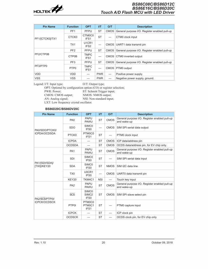
Pin Name Function OPT I/T O/T Description
PF1/[CTCK0]/TX1
PF1 PFPU ST CMOS General purpose I/O. Register enabled pull-up
CTCK0 CTM0C0IFS1 ST — CTM0 clock input
TX1 U1CR1IFS2 — CMOS UART1 data transmit pin
PF2/CTP0BPF2 PFPU ST CMOS General purpose I/O. Register enabled pull-up
CTP0B TMPCIFS1 — CMOS CTM0 inverted output
PF3/PTP0PF3 PFPU ST CMOS General purpose I/O. Register enabled pull-up
PTP0 TMPCIFS1 — CMOS PTM0 output
VDD VDD — PWR — Positive power supplyVSS VSS — PWR — Negative power supply, ground.
Legend: I/T: Input type; O/T: Output type;OPT: Optional by configuration option (CO) or register selection;PWR: Power; ST: Schmitt Trigger input;CMOS: CMOS output; NMOS: NMOS output;AN: Analog signal; NSI: Non-standard input;LXT: Low frequency crystal oscillator.
BS86D20C/BS86DV20CPin Name Function OPT I/T O/T Description
PA0/SDO/PTCK0/ICPDA/OCDSDA
PA0 PAPUPAWU ST CMOS General purpose I/O. Register enabled pull-up
and wake-up
SDO SIMC0IFS0 — CMOS SIM SPI serial data output
PTCK0 PTM0C0IFS1 ST — PTM0 clock input
ICPDA — ST CMOS ICP data/address pinOCDSDA — ST CMOS OCDS data/address pin, for EV chip only.
PA1/[SDI/SDA]/[TX0]/KEY20
PA1 PAPUPAWU ST CMOS General purpose I/O. Register enabled pull-up
and wake-up
SDI SIMC0IFS0 ST — SIM SPI serial data input
SDA SIMC0IFS0 ST NMOS SIM I2C data line
TX0 U0CR1IFS0 — CMOS UART0 data transmit pin
KEY20 TKM4C1 NSI — Touch key input
PA2/SCS/PTP0I/ICPCK/OCDSCK
PA2 PAPUPAWU ST CMOS General purpose I/O. Register enabled pull-up
and wake-up
SCSSIMC0SIMC2IFS0
ST CMOS SIM SPI slave select pin
PTP0IPTM0C0PTM0C1
IFS1ST — PTM0 capture input
ICPCK — ST — ICP clock pinOCDSCK — ST — OCDS clock pin, for EV chip only

Rev. 1.10 20 October 09, 2018 Rev. 1.10 21 October 09, 2018
BS86C08C/BS86D12CBS86E16C/BS86D20C
Touch A/D Flash MCU with LED Driver
BS86C08C/BS86D12CBS86E16C/BS86D20CTouch A/D Flash MCU with LED Driver
Pin Name Function OPT I/T O/T Description
PA3/SDI/SDA/RX0
PA3 PAPUPAWU ST CMOS General purpose I/O. Register enabled pull-up
and wake-up
SDI SIMC0IFS0 ST — SIM SPI serial data input
SDA SIMC0IFS0 ST NMOS SIM I2C data line
RX0U0CR1
IFS0IFS1
ST — UART0 data receive pin
PA4/INT/CTCK0/[SCK/SCL]/[RX0]/KEY19
PA4 PAPUPAWU ST CMOS General purpose I/O. Register enabled pull-up
and wake-up
INT INTC0INTEG ST — External interrupt input
CTCK0 CTM0C0 ST — CTM0 clock input
SCK SIMC0IFS0 ST CMOS SIM SPI serial clock
SCL SIMC0IFS0 ST NMOS SIM I2C clock line
RX0U0CR1
IFS0IFS1
ST — UART0 data receive pin
KEY19 TKM4C1 NSI — Touch key input
PA7/SCK/SCL/TX0
PA7 PAPUPAWU ST CMOS General purpose I/O. Register enabled pull-up
and wake-up
SCK SIMC0IFS0 ST CMOS SIM SPI serial clock
SCL SIMC0IFS0 ST NMOS SIM I2C clock line
TX0 U0CR1IFS0 — CMOS UART0 data transmit pin
PB0/KEY1~PB3/KEY4PB0~PB3 PBPU ST CMOS General purpose I/O. Register enabled pull-up
KEY1~KEY4 TKM0C1 NSI — Touch key input
PB4/KEY5PB4 PBPU ST CMOS General purpose I/O. Register enabled pull-up
KEY5 TKM1C1 NSI — Touch key input
PB5/PTCK1/KEY6PB5 PBPU ST CMOS General purpose I/O. Register enabled pull-up
PTCK1 PTM1C0 ST — PTM1 clock inputKEY6 TKM1C1 NSI — Touch key input
PB6/PTP1/KEY7PB6 PBPU ST CMOS General purpose I/O. Register enabled pull-up
PTP1 TMPC — CMOS PTM1 outputKEY7 TKM1C1 NSI — Touch key input
PB7/PTP1I/KEY8
PB7 PBPU ST CMOS General purpose I/O. Register enabled pull-up
PTP1I PTM1C0PTM1C1 ST — PTM1 capture input
KEY8 TKM1C1 NSI — Touch key input
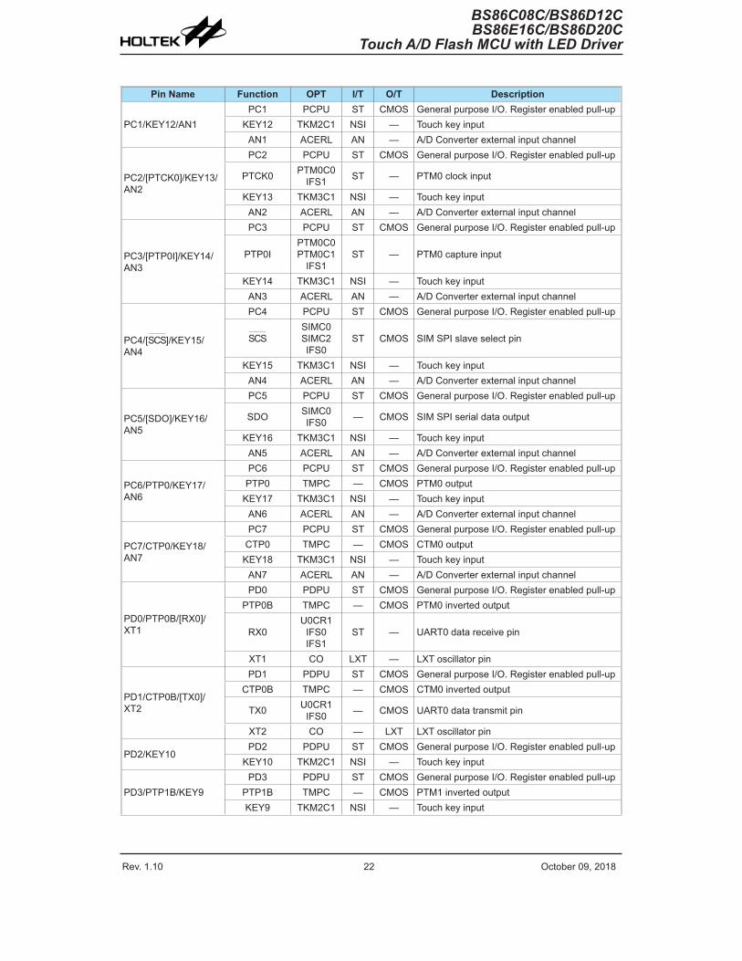
PC0/KEY11/AN0/VREF
PC0 PCPU ST CMOS General purpose I/O. Register enabled pull-upKEY11 TKM2C1 NSI — Touch key inputAN0 ACERL AN — A/D Converter external input channel
VREF TMPC AN — A/D Converter external reference voltage input
Rev. 1.10 22 October 09, 2018 Rev. 1.10 23 October 09, 2018
BS86C08C/BS86D12CBS86E16C/BS86D20C
Touch A/D Flash MCU with LED Driver
BS86C08C/BS86D12CBS86E16C/BS86D20CTouch A/D Flash MCU with LED Driver
Pin Name Function OPT I/T O/T Description
PC1/KEY12/AN1PC1 PCPU ST CMOS General purpose I/O. Register enabled pull-up
KEY12 TKM2C1 NSI — Touch key inputAN1 ACERL AN — A/D Converter external input channel
PC2/[PTCK0]/KEY13/AN2
PC2 PCPU ST CMOS General purpose I/O. Register enabled pull-up
PTCK0 PTM0C0IFS1 ST — PTM0 clock input
KEY13 TKM3C1 NSI — Touch key inputAN2 ACERL AN — A/D Converter external input channel
PC3/[PTP0I]/KEY14/AN3
PC3 PCPU ST CMOS General purpose I/O. Register enabled pull-up
PTP0IPTM0C0PTM0C1
IFS1ST — PTM0 capture input
KEY14 TKM3C1 NSI — Touch key inputAN3 ACERL AN — A/D Converter external input channel
PC4/[SCS]/KEY15/AN4
PC4 PCPU ST CMOS General purpose I/O. Register enabled pull-up
SCSSIMC0SIMC2IFS0
ST CMOS SIM SPI slave select pin
KEY15 TKM3C1 NSI — Touch key inputAN4 ACERL AN — A/D Converter external input channel
PC5/[SDO]/KEY16/AN5
PC5 PCPU ST CMOS General purpose I/O. Register enabled pull-up
SDO SIMC0IFS0 — CMOS SIM SPI serial data output
KEY16 TKM3C1 NSI — Touch key inputAN5 ACERL AN — A/D Converter external input channel
PC6/PTP0/KEY17/AN6
PC6 PCPU ST CMOS General purpose I/O. Register enabled pull-upPTP0 TMPC — CMOS PTM0 output
KEY17 TKM3C1 NSI — Touch key inputAN6 ACERL AN — A/D Converter external input channel
PC7/CTP0/KEY18/AN7
PC7 PCPU ST CMOS General purpose I/O. Register enabled pull-upCTP0 TMPC — CMOS CTM0 output
KEY18 TKM3C1 NSI — Touch key inputAN7 ACERL AN — A/D Converter external input channel
PD0/PTP0B/[RX0]/XT1
PD0 PDPU ST CMOS General purpose I/O. Register enabled pull-upPTP0B TMPC — CMOS PTM0 inverted output
RX0U0CR1
IFS0IFS1
ST — UART0 data receive pin
XT1 CO LXT — LXT oscillator pin
PD1/CTP0B/[TX0]/XT2
PD1 PDPU ST CMOS General purpose I/O. Register enabled pull-upCTP0B TMPC — CMOS CTM0 inverted output
TX0 U0CR1IFS0 — CMOS UART0 data transmit pin
XT2 CO — LXT LXT oscillator pin
PD2/KEY10PD2 PDPU ST CMOS General purpose I/O. Register enabled pull-up
KEY10 TKM2C1 NSI — Touch key input
PD3/PTP1B/KEY9PD3 PDPU ST CMOS General purpose I/O. Register enabled pull-up
PTP1B TMPC — CMOS PTM1 inverted outputKEY9 TKM2C1 NSI — Touch key input
Rev. 1.10 22 October 09, 2018 Rev. 1.10 23 October 09, 2018
BS86C08C/BS86D12CBS86E16C/BS86D20C
Touch A/D Flash MCU with LED Driver
BS86C08C/BS86D12CBS86E16C/BS86D20CTouch A/D Flash MCU with LED Driver
Pin Name Function OPT I/T O/T DescriptionVDD VDD — PWR — Positive power supplyVSS VSS — PWR — Negative power supply, ground.
Legend: I/T: Input type; O/T: Output type;OPT: Optional by configuration option (CO) or register selection;PWR: Power; ST: Schmitt Trigger input;CMOS: CMOS output; NMOS: NMOS output;AN: Analog signal; NSI: Non-standard input;LXT: Low frequency crystal oscillator.
Absolute Maximum RatingsSupply Voltage ........................................................................................................ VSS-0.3V to +6.0V
Input Voltage ..................................................................................................... VSS-0.3V to VDD+0.3V
Storage Temperature ..................................................................................................... -50°C to 125°C
Operating Temperature ................................................................................................... -40°C to 85°C
IOH Total ...................................................................................................................................... -80mA
IOL Total ..................................................................................................................................... 100mA
Total Power Dissipation ........................................................................................................... 500mW
Note: These are stress ratings only. Stresses exceeding the range specified under “Absolute Maximum Ratings” may cause substantial damage to these devices. Functional operation of these devices at other conditions beyond those listed in the specification is not implied and prolonged exposure to extreme conditions may affect device reliability.
D.C. Electrical CharacteristicsFor data in the following tables, note that factors such as oscillator type, operating voltage, operating frequency, pin load conditions, temperature and program instruction type, can all exert an influence on the measured values.
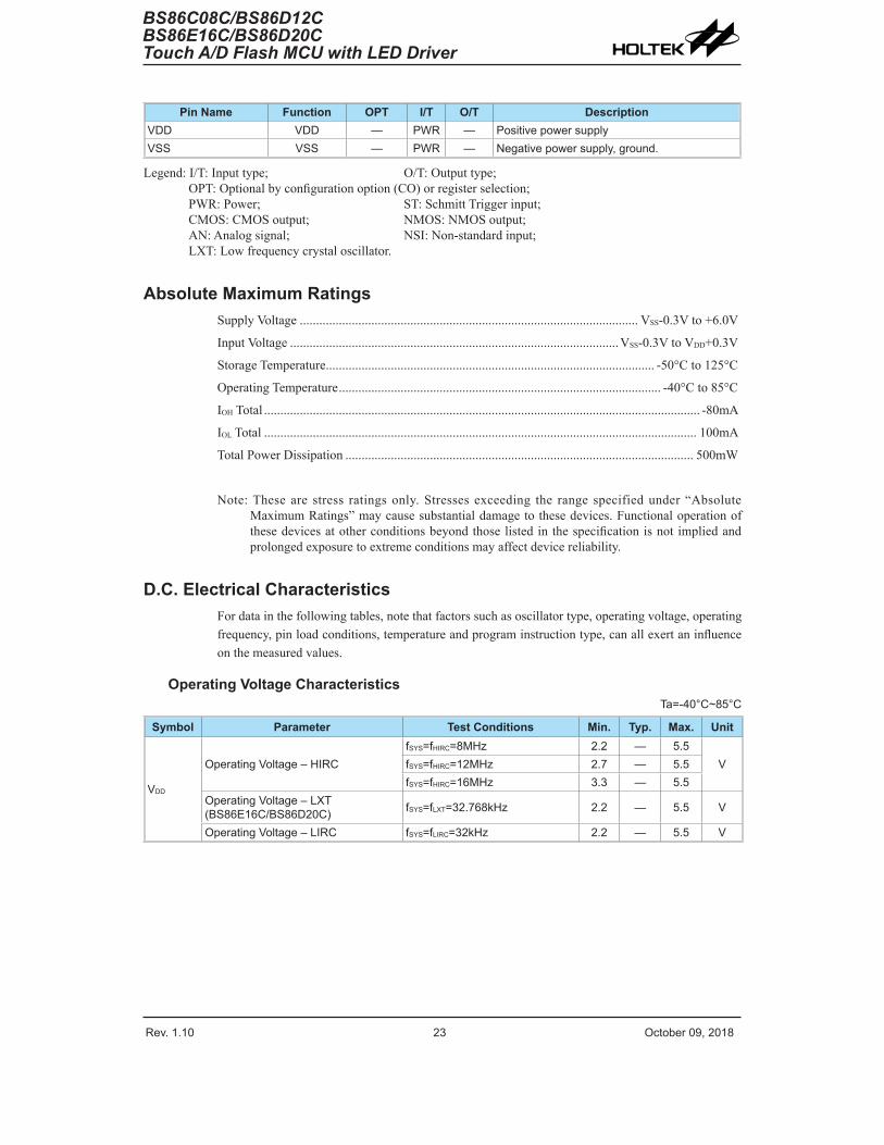
Operating Voltage CharacteristicsTa=-40°C~85°C
Symbol Parameter Test Conditions Min. Typ. Max. Unit
VDD
Operating Voltage – HIRCfSYS=fHIRC=8MHz 2.2 — 5.5
VfSYS=fHIRC=12MHz 2.7 — 5.5fSYS=fHIRC=16MHz 3.3 — 5.5
Operating Voltage – LXT(BS86E16C/BS86D20C) fSYS=fLXT=32.768kHz 2.2 — 5.5 V
Operating Voltage – LIRC fSYS=fLIRC=32kHz 2.2 — 5.5 V

Rev. 1.10 24 October 09, 2018 Rev. 1.10 25 October 09, 2018
BS86C08C/BS86D12CBS86E16C/BS86D20C
Touch A/D Flash MCU with LED Driver
BS86C08C/BS86D12CBS86E16C/BS86D20CTouch A/D Flash MCU with LED Driver
Operating Current CharacteristicsTa=25°C
Symbol ParameterTest Conditions
Min. Typ. Max. UnitVDD Conditions
IDD
SLOW Mode – LIRC2.2V
fSYS=fLIRC=32kHz, LVR enable— 25 50
μA3V — 28 565V — 36 72
SLOW Mode – LXT(BS86E16C/BS86D20C)
2.2VfSYS=fLXT=32768Hz, LXTLP=0
— 27 55μA3V — 30 60
5V — 48 962.2V
fSYS=fLXT=32768Hz, LXTLP=1— 24 48
μA3V — 25 505V — 36 72
FAST Mode – HIRC
2.2VfSYS=fHIRC=8MHz
— 1 1.6mA3V — 1.2 1.8
5V — 2.2 3.32.7V
fSYS=fHIRC=12MHz— 1.4 2.2
mA3V — 1.6 2.45V — 3.3 5
3.3VfSYS=fHIRC=16MHz
— 2.0 3.5mA
5V — 4.0 6.0
Note: When using the characteristic table data, the following notes should be taken into consideration:1. Any digital input is setup in a non-floating condition.2. All measurements are taken under conditions of no load and with all peripherals in an off state.3. There are no DC current paths.4. All Operating Current values are measured using a continuous NOP instruction program loop.

Rev. 1.10 24 October 09, 2018 Rev. 1.10 25 October 09, 2018
BS86C08C/BS86D12CBS86E16C/BS86D20C
Touch A/D Flash MCU with LED Driver
BS86C08C/BS86D12CBS86E16C/BS86D20CTouch A/D Flash MCU with LED Driver
Standby Current CharacteristicsTa=25°C, unless otherwise specified
Symbol ParameterTest Conditions
Min. Typ. Max. Max.@85°C Unit
VDD Conditions
ISTB
SLEEP Mode2.2V
WDT on— 1.2 2.4 3.0
μA3V — 1.5 3 3.75V — 3 5 6
IDLE0 Mode – LIRC2.2V
fSUB=fLIRC on— 2.4 4 4.6
μA3V — 3 5 5.75V — 5 10 11
IDLE0 Mode – LXT(BS86E16C/BS86D20C)
2.2VfSUB=fLXT on, LXTLP=0
— 4 8 8μA3V — 5 10 11
5V — 18 30 322.2V
fSUB=fLXT on, LXTLP=1— 2 4 4.6
μA3V — 2.5 5 5.75V — 6 10 11
IDLE1 Mode – HIRC
2.2VfSUB on, fSYS=8MHz
— 0.6 1 1mA3V — 0.8 1.2 1.2
5V — 1.0 2.0 2.02.7V
fSUB on, fSYS=12MHz— 0.7 1.2 1.2
mA3V — 0.9 1.4 1.45V — 1.4 2.1 2.1
3.3VfSUB on, fSYS=16MHz
— 1.6 3.2 3.2mA
5V — 2.0 4.0 4.0
Note: When using the characteristic table data, the following notes should be taken into consideration:1. Any digital input is setup in a non-floating condition.2. All measurements are taken under conditions of no load and with all peripherals in an off state.3. There are no DC current paths.4. All Standby Current values are taken after a HALT instruction executed thus stopping all instruction
execution.
Rev. 1.10 26 October 09, 2018 Rev. 1.10 27 October 09, 2018
BS86C08C/BS86D12CBS86E16C/BS86D20C
Touch A/D Flash MCU with LED Driver
BS86C08C/BS86D12CBS86E16C/BS86D20CTouch A/D Flash MCU with LED Driver
A.C. CharacteristicsFor data in the following tables, note that factors such as oscillator type, operating voltage, operating frequency and temperature etc., can all exert an influence on the measured values.
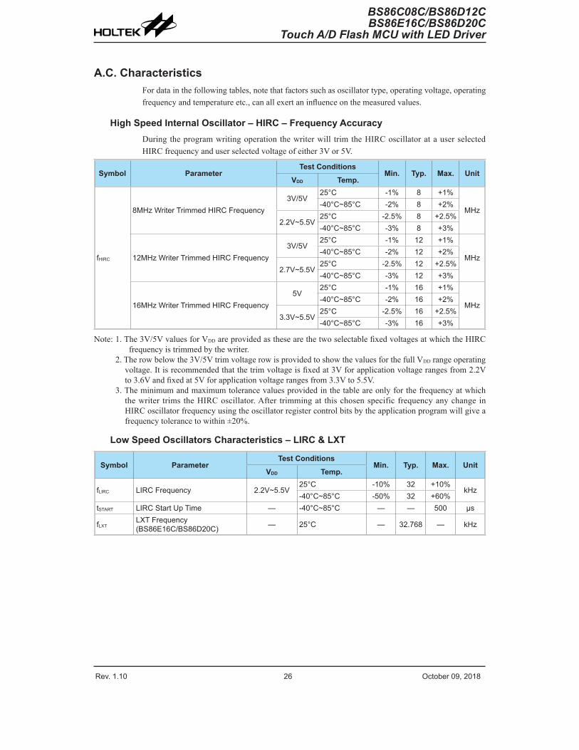
High Speed Internal Oscillator – HIRC – Frequency AccuracyDuring the program writing operation the writer will trim the HIRC oscillator at a user selected HIRC frequency and user selected voltage of either 3V or 5V.
Symbol ParameterTest Conditions
Min. Typ. Max. UnitVDD Temp.
fHIRC
8MHz Writer Trimmed HIRC Frequency3V/5V
25°C -1% 8 +1%
MHz-40°C~85°C -2% 8 +2%
2.2V~5.5V25°C -2.5% 8 +2.5%-40°C~85°C -3% 8 +3%
12MHz Writer Trimmed HIRC Frequency3V/5V
25°C -1% 12 +1%
MHz-40°C~85°C -2% 12 +2%
2.7V~5.5V25°C -2.5% 12 +2.5%-40°C~85°C -3% 12 +3%
16MHz Writer Trimmed HIRC Frequency5V
25°C -1% 16 +1%
MHz-40°C~85°C -2% 16 +2%
3.3V~5.5V25°C -2.5% 16 +2.5%-40°C~85°C -3% 16 +3%
Note: 1. The 3V/5V values for VDD are provided as these are the two selectable fixed voltages at which the HIRC frequency is trimmed by the writer.
2. The row below the 3V/5V trim voltage row is provided to show the values for the full VDD range operating voltage. It is recommended that the trim voltage is fixed at 3V for application voltage ranges from 2.2V to 3.6V and fixed at 5V for application voltage ranges from 3.3V to 5.5V.
3. The minimum and maximum tolerance values provided in the table are only for the frequency at which the writer trims the HIRC oscillator. After trimming at this chosen specific frequency any change in HIRC oscillator frequency using the oscillator register control bits by the application program will give a frequency tolerance to within ±20%.
Low Speed Oscillators Characteristics – LIRC & LXT
Symbol ParameterTest Conditions
Min. Typ. Max. UnitVDD Temp.
fLIRC LIRC Frequency 2.2V~5.5V25°C -10% 32 +10%
kHz-40°C~85°C -50% 32 +60%
tSTART LIRC Start Up Time — -40°C~85°C — — 500 μs
fLXTLXT Frequency(BS86E16C/BS86D20C) — 25°C — 32.768 — kHz
Rev. 1.10 26 October 09, 2018 Rev. 1.10 27 October 09, 2018
BS86C08C/BS86D12CBS86E16C/BS86D20C
Touch A/D Flash MCU with LED Driver
BS86C08C/BS86D12CBS86E16C/BS86D20CTouch A/D Flash MCU with LED Driver
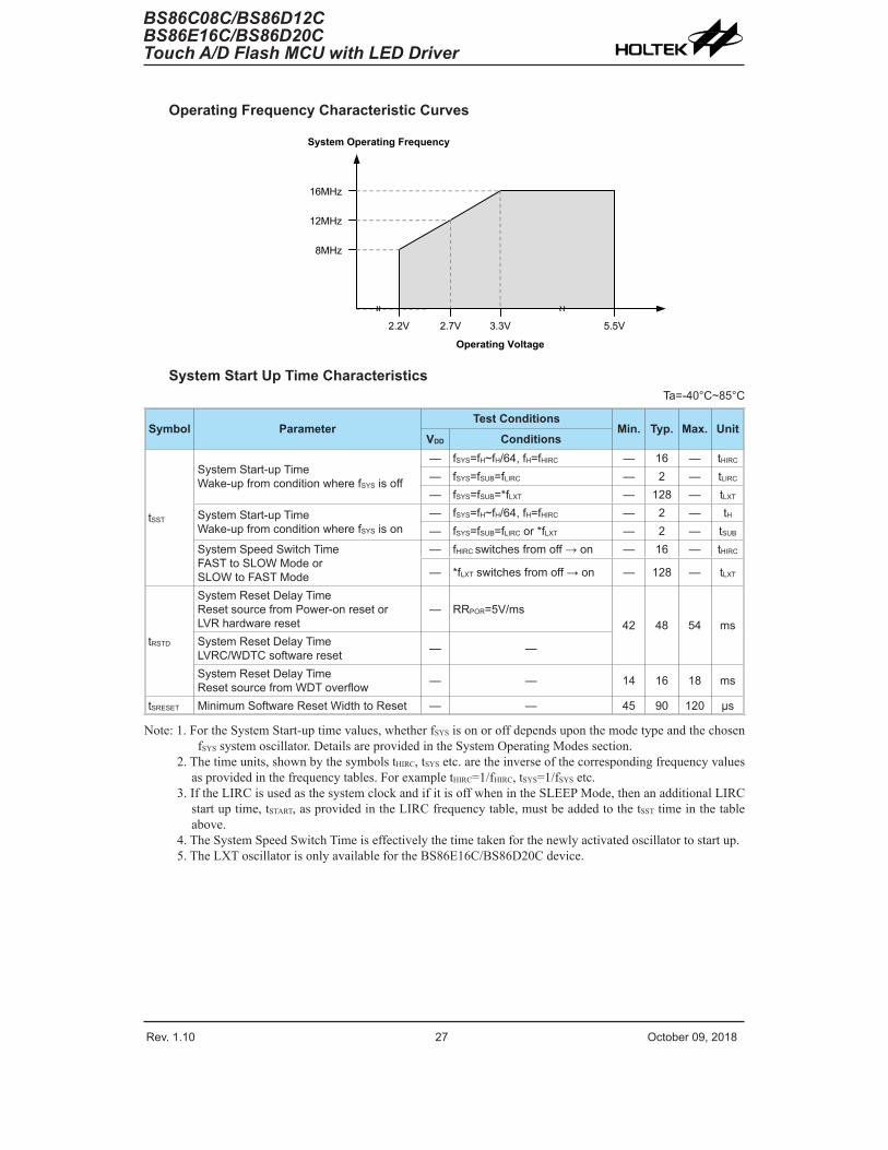
Operating Frequency Characteristic Curves
System Operating Frequency
Operating Voltage
12MHz
16MHz
2.2V 2.7V 3.3V 5.5V~ ~~~
8MHz
System Start Up Time CharacteristicsTa=-40°C~85°C
Symbol ParameterTest Conditions
Min. Typ. Max. UnitVDD Conditions
tSST
System Start-up TimeWake-up from condition where fSYS is off
— fSYS=fH~fH/64, fH=fHIRC — 16 — tHIRC
— fSYS=fSUB=fLIRC — 2 — tLIRC
— fSYS=fSUB=*fLXT — 128 — tLXT
System Start-up TimeWake-up from condition where fSYS is on
— fSYS=fH~fH/64, fH=fHIRC — 2 — tH— fSYS=fSUB=fLIRC or *fLXT — 2 — tSUB
System Speed Switch TimeFAST to SLOW Mode orSLOW to FAST Mode
— fHIRC switches from off → on — 16 — tHIRC
— *fLXT switches from off → on — 128 — tLXT
tRSTD
System Reset Delay TimeReset source from Power-on reset or LVR hardware reset
— RRPOR=5V/ms42 48 54 ms
System Reset Delay TimeLVRC/WDTC software reset — —
System Reset Delay TimeReset source from WDT overflow — — 14 16 18 ms
tSRESET Minimum Software Reset Width to Reset — — 45 90 120 μs
Note: 1. For the System Start-up time values, whether fSYS is on or off depends upon the mode type and the chosen fSYS system oscillator. Details are provided in the System Operating Modes section.
2. The time units, shown by the symbols tHIRC, tSYS etc. are the inverse of the corresponding frequency values as provided in the frequency tables. For example tHIRC=1/fHIRC, tSYS=1/fSYS etc.
3. If the LIRC is used as the system clock and if it is off when in the SLEEP Mode, then an additional LIRC start up time, tSTART, as provided in the LIRC frequency table, must be added to the tSST time in the table above.
4. The System Speed Switch Time is effectively the time taken for the newly activated oscillator to start up.5. The LXT oscillator is only available for the BS86E16C/BS86D20C device.

Rev. 1.10 28 October 09, 2018 Rev. 1.10 29 October 09, 2018
BS86C08C/BS86D12CBS86E16C/BS86D20C
Touch A/D Flash MCU with LED Driver
BS86C08C/BS86D12CBS86E16C/BS86D20CTouch A/D Flash MCU with LED Driver
Input/Output CharacteristicsTa=25°C
Symbol ParameterTest Conditions
Min. Typ. Max. UnitVDD Conditions
VIL Input Low Voltage for I/O Ports5V
—0 — 1.5
V— 0 — 0.2VDD
VIH Input High Voltage for I/O Ports5V
—3.5 — 5.0
V— 0.8VDD — VDD
IOL
Sink Current for I/O Ports(PA, PC, PD, PE, PF)
3V
VOL=0.1VDD,PxNS=0, x=A, C, D, E or F 16 32 —
mA
VOL=0.1VDD,PxNS=1, x=A, C, D, E or F 25 50 —
5V
VOL=0.1VDD,PxNS=0, x=A, C, D, E or F 32 64 —
VOL=0.1VDD,PxNS=1, x=A, C, D, E or F 50 100 —
Sink Current for I/O Ports (PB)3V
VOL=0.1VDD16 32 —
mA5V 32 64 —
IOH Source Current for I/O Ports
3VVOH=0.9VDD, PxPS=00
-1.0 -2.0 —
mA
5V -2.0 -4.0 —3V
VOH=0.9VDD, PxPS=01-1.75 -3.5 —
5V -3.5 -7.0 —3V
VOH=0.9VDD, PxPS=10-2.5 -5.0 —
5V -5.0 -10 —3V
VOH=0.9VDD, PxPS=11-5.5 -11 —
5V -11 -22 —
RPH Pull-high Resistance for I/O Ports (Note)3V
—20 60 100
kΩ5V 10 30 50
tTCK TM Clock Input Pin Minimum Pulse Width — — 0.3 — — μs
tTPITM Capture Input Pin Minimum Pulse Width — — 0.3 — — μs
fTMCLKTM Maximum Timer Clock Source Frequency 5V — — — 1 fSYS
tCPW TM Minimum Capture Pulse Width — — 2 — — tTMCLK
tINT External Interrupt Minimum Pulse Width — — 10 — — μs
Note: The RPH internal pull high resistance value is calculated by connecting to ground and enabling the input pin with a pull-high resistor and then measuring the pin current at the specified supply voltage level. Dividing the voltage by this measured current provides the RPH value.

Rev. 1.10 28 October 09, 2018 Rev. 1.10 29 October 09, 2018
BS86C08C/BS86D12CBS86E16C/BS86D20C
Touch A/D Flash MCU with LED Driver
BS86C08C/BS86D12CBS86E16C/BS86D20CTouch A/D Flash MCU with LED Driver
Memory CharacteristicsTa=-40°C~85°C, unless otherwise specified
Symbol ParameterTest Conditions
Min. Typ. Max. UnitVDD Conditions
VRW VDD for Read / Write — — VDDmin — VDDmax VFlash Program / Data EEPROM Memory
tDEW
Erase / Write Cycle Time – Flash Program Memory — — — 2 3 ms
Write Cycle Time – Data EEPROM Memory — — — 4 6 ms
IDDPGM Programming / Erase Current on VDD — — — — 5.0 mAEP Cell Endurance — — 100K — — E/WtRETD ROM Data Retention Time — Ta=25°C — 40 — YearRAM Data MemoryVDR RAM Data Retention Voltage — Device in SLEEP Mode 1.0 — — V
LVD/LVR Electrical CharacteristicsTa=-40°C~85°C
Symbol ParameterTest Conditions
Min. Typ. Max. UnitVDD Conditions
VLVR Low Voltage Reset Voltage
— LVR enable, voltage select 2.1V
-5%
2.1
+5% V— LVR enable, voltage select 2.55V 2.55— LVR enable, voltage select 3.15V 3.15— LVR enable, voltage select 3.8V 3.8
VLVD Low Voltage Detection Voltage
— LVD enable, voltage select 2.0V
-5%
2.0
+5% V
— LVD enable, voltage select 2.2V 2.2— LVD enable, voltage select 2.4V 2.4— LVD enable, voltage select 2.7V 2.7— LVD enable, voltage select 3.0V 3.0— LVD enable, voltage select 3.3V 3.3— LVD enable, voltage select 3.6V 3.6— LVD enable, voltage select 4.0V 4.0
ILVRLVDBG Operating Current
3V LVD enable, LVR enable, VBGEN = 0
— — 18 μA5V — 20 25 μA3V LVD enable, LVR enable,
VBGEN = 1— — 150 μA
5V — 180 200 μA
tLVDS LVDO Stable Time — For LVR enable, VBGEN=0,LVD off → on — — 15 μs
tLVR Minimum Low Voltage Width to Reset — — 120 240 480 μs
tLVDMinimum Low Voltage Width to Interrupt — — 60 120 240 μs

Rev. 1.10 30 October 09, 2018 Rev. 1.10 31 October 09, 2018
BS86C08C/BS86D12CBS86E16C/BS86D20C
Touch A/D Flash MCU with LED Driver
BS86C08C/BS86D12CBS86E16C/BS86D20CTouch A/D Flash MCU with LED Driver
A/D Converter Electrical CharacteristicsTa=-40°C~85°C
Symbol ParameterTest Conditions
Min. Typ. Max. UnitVDD Conditions
VDD Operating Voltage — — 2.2 — 5.5 VVADI Input Voltage — — 0 — VREF VVREF Reference Voltage — — 2 — VDD VNR Resolution — — — — 12 BitDNL Differential Non-linearity — VREF=VDD, tADCK=0.5μs -3 — +3 LSBINL Integral Non-linearity — VREF=VDD, tADCK=0.5μs -4 — +4 LSB
IADCAdditional Current Consumption for A/D Converter Enable
2.2VNo load, tADCK=0.5μs
— 300 420 μA3V
—340 500 μA
5V 500 700 μAtADCK Clock Period — — 0.5 — 10 μstON2ST A/D Converter On-to-Start Time — — 4 — — μs
tADCConversion Time(Including A/D Sample and Hold Time) — — — 16 — tADCK
Internal Reference Voltage CharacteristicsTa=-40°C~85°C
Symbol ParameterTest Conditions
Min. Typ. Max. UnitVDD Conditions
VBG Bandgap Reference Voltage — — -3% 1.09 +3% V
IBGAdditional Current for Bandgap Reference Enable — — — 200 300 μA
tBGS VBG Turn-on Stable Time — No load — — 200 μs
Note: 1. All the above parameters are measured under conditions of no load condition unless otherwise described.2. A 0.1μF ceramic capacitor should be connected between VDD and GND.3. The VBG voltage is used as the A/D converter internal signal input.
Power-on Reset CharacteristicsTa=25°C
Symbol ParameterTest Conditions
Min. Typ. Max. UnitVDD Conditions
VPOR VDD Start Voltage to Ensure Power-on Reset — — — — 100 mVRRPOR VDD Rising Rate to Ensure Power-on Reset — — 0.035 — — V/ms
tPORMinimum Time for VDD Stays at VPOR to Ensure Power-on Reset — — 1 — — ms
VDD
tPOR RRPOR
VPOR
Time
Rev. 1.10 30 October 09, 2018 Rev. 1.10 31 October 09, 2018
BS86C08C/BS86D12CBS86E16C/BS86D20C
Touch A/D Flash MCU with LED Driver
BS86C08C/BS86D12CBS86E16C/BS86D20CTouch A/D Flash MCU with LED Driver
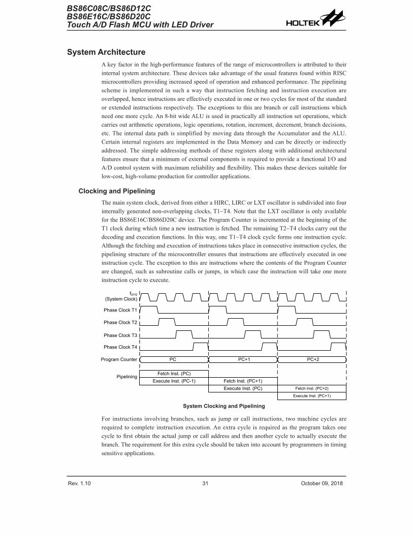
System ArchitectureA key factor in the high-performance features of the range of microcontrollers is attributed to their internal system architecture. These devices take advantage of the usual features found within RISC microcontrollers providing increased speed of operation and enhanced performance. The pipelining scheme is implemented in such a way that instruction fetching and instruction execution are overlapped, hence instructions are effectively executed in one or two cycles for most of the standard or extended instructions respectively. The exceptions to this are branch or call instructions which need one more cycle. An 8-bit wide ALU is used in practically all instruction set operations, which carries out arithmetic operations, logic operations, rotation, increment, decrement, branch decisions, etc. The internal data path is simplified by moving data through the Accumulator and the ALU. Certain internal registers are implemented in the Data Memory and can be directly or indirectly addressed. The simple addressing methods of these registers along with additional architectural features ensure that a minimum of external components is required to provide a functional I/O and A/D control system with maximum reliability and flexibility. This makes these devices suitable for low-cost, high-volume production for controller applications.
Clocking and PipeliningThe main system clock, derived from either a HIRC, LIRC or LXT oscillator is subdivided into four internally generated non-overlapping clocks, T1~T4. Note that the LXT oscillator is only available for the BS86E16C/BS86D20C device. The Program Counter is incremented at the beginning of the T1 clock during which time a new instruction is fetched. The remaining T2~T4 clocks carry out the decoding and execution functions. In this way, one T1~T4 clock cycle forms one instruction cycle. Although the fetching and execution of instructions takes place in consecutive instruction cycles, the pipelining structure of the microcontroller ensures that instructions are effectively executed in one instruction cycle. The exception to this are instructions where the contents of the Program Counter are changed, such as subroutine calls or jumps, in which case the instruction will take one more instruction cycle to execute.
Fetch Inst. (PC)
(System Clock)fSYS
Phase Clock T1
Phase Clock T2
Phase Clock T3
Phase Clock T4
Program Counter PC PC+1 PC+2
PipeliningExecute Inst. (PC-1) Fetch Inst. (PC+1)
Execute Inst. (PC) Fetch Inst. (PC+2)
Execute Inst. (PC+1)
System Clocking and Pipelining
For instructions involving branches, such as jump or call instructions, two machine cycles are required to complete instruction execution. An extra cycle is required as the program takes one cycle to first obtain the actual jump or call address and then another cycle to actually execute the branch. The requirement for this extra cycle should be taken into account by programmers in timing sensitive applications.

Rev. 1.10 32 October 09, 2018 Rev. 1.10 33 October 09, 2018
BS86C08C/BS86D12CBS86E16C/BS86D20C
Touch A/D Flash MCU with LED Driver
BS86C08C/BS86D12CBS86E16C/BS86D20CTouch A/D Flash MCU with LED Driver
Fetch Inst. 11 MOV A,[12H]2 CALL DELAY3 CPL [12H]4 :5 :6 DELAY: NOP
Execute Inst. 1 Fetch Inst. 2 Execute Inst. 2
Fetch Inst. 3 Flush PipelineFetch Inst. 6 Execute Inst. 6
Fetch Inst. 7
Instruction Fetching
Program CounterDuring program execution, the Program Counter is used to keep track of the address of the next instruction to be executed. It is automatically incremented by one each time an instruction is executed except for instructions, such as “JMP” or “CALL” that demand a jump to a non-consecutive Program Memory address. For the device whose memory capacity is greater than 8K words, the Program Memory address may be located in a certain program memory bank which is selected by the program memory bank pointer bit, PBP0. Only the lower 8 bits, known as the Program Counter Low Register, are directly addressable by the application program.
When executing instructions requiring jumps to non-consecutive addresses such as a jump instruction, a subroutine call, interrupt or reset, etc., the microcontroller manages program control by loading the required address into the Program Counter. For conditional skip instructions, once the condition has been met, the next instruction, which has already been fetched during the present instruction execution, is discarded and a dummy cycle takes its place while the correct instruction is obtained.
DeviceProgram Counter
High Byte Low Byte (PCL)BS86C08C PC11~PC8 PCL7~PCL0BS86D12C PC12~PC8 PCL7~PCL0BS86E16C PBP0, PC12~PC8 PCL7~PCL0BS86D20C PC12~PC8 PCL7~PCL0
Program Counter
The lower byte of the Program Counter, known as the Program Counter Low register or PCL, is available for program control and is a readable and writeable register. By transferring data directly into this register, a short program jump can be executed directly; however, as only this low byte is available for manipulation, the jumps are limited to the present page of memory that is 256 locations. When such program jumps are executed it should also be noted that a dummy cycle will be inserted. Manipulating the PCL register may cause program branching, so an extra cycle is needed to pre-fetch.
StackThis is a special part of the memory which is used to save the contents of the Program Counter only. The stack is organized into 8 levels and neither part of the data nor part of the program space, and is neither readable nor writeable. The activated level is indexed by the Stack Pointer, and is neither readable nor writeable. At a subroutine call or interrupt acknowledge signal, the contents of the Program Counter are pushed onto the stack. At the end of a subroutine or an interrupt routine, signaled by a return instruction, RET or RETI, the Program Counter is restored to its previous value from the stack. After a device reset, the Stack Pointer will point to the top of the stack.
If the stack is full and an enabled interrupt takes place, the interrupt request flag will be recorded but the acknowledge signal will be inhibited. When the Stack Pointer is decremented, by RET or RETI, the interrupt will be serviced. This feature prevents stack overflow allowing the programmer to use
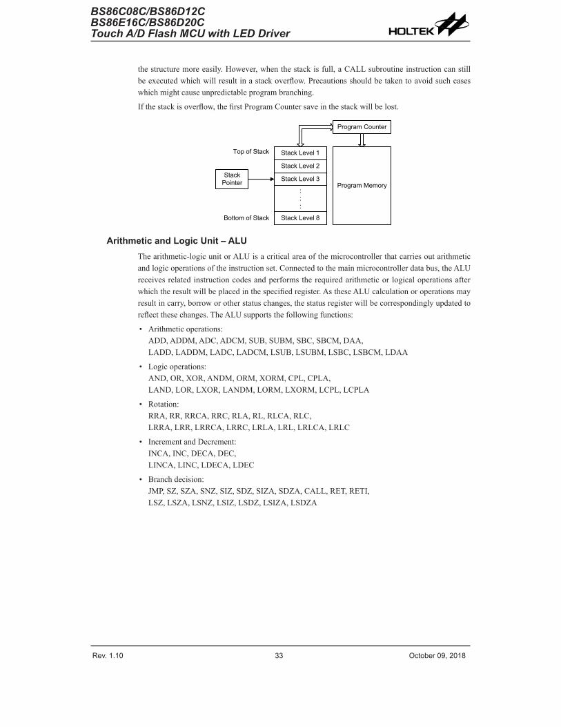
Rev. 1.10 32 October 09, 2018 Rev. 1.10 33 October 09, 2018
BS86C08C/BS86D12CBS86E16C/BS86D20C
Touch A/D Flash MCU with LED Driver
BS86C08C/BS86D12CBS86E16C/BS86D20CTouch A/D Flash MCU with LED Driver
the structure more easily. However, when the stack is full, a CALL subroutine instruction can still be executed which will result in a stack overflow. Precautions should be taken to avoid such cases which might cause unpredictable program branching.
If the stack is overflow, the first Program Counter save in the stack will be lost.
StackPointer
Stack Level 2
Stack Level 1
Stack Level 3
:::
Stack Level 8
Program Memory
Program Counter
Bottom of Stack
Top of Stack
Arithmetic and Logic Unit – ALUThe arithmetic-logic unit or ALU is a critical area of the microcontroller that carries out arithmetic and logic operations of the instruction set. Connected to the main microcontroller data bus, the ALU receives related instruction codes and performs the required arithmetic or logical operations after which the result will be placed in the specified register. As these ALU calculation or operations may result in carry, borrow or other status changes, the status register will be correspondingly updated to reflect these changes. The ALU supports the following functions:
• Arithmetic operations: ADD, ADDM, ADC, ADCM, SUB, SUBM, SBC, SBCM, DAA,LADD, LADDM, LADC, LADCM, LSUB, LSUBM, LSBC, LSBCM, LDAA
• Logic operations: AND, OR, XOR, ANDM, ORM, XORM, CPL, CPLA, LAND, LOR, LXOR, LANDM, LORM, LXORM, LCPL, LCPLA
• Rotation:RRA, RR, RRCA, RRC, RLA, RL, RLCA, RLC,LRRA, LRR, LRRCA, LRRC, LRLA, LRL, LRLCA, LRLC
• Increment and Decrement:INCA, INC, DECA, DEC,LINCA, LINC, LDECA, LDEC
• Branch decision:JMP, SZ, SZA, SNZ, SIZ, SDZ, SIZA, SDZA, CALL, RET, RETI,LSZ, LSZA, LSNZ, LSIZ, LSDZ, LSIZA, LSDZA
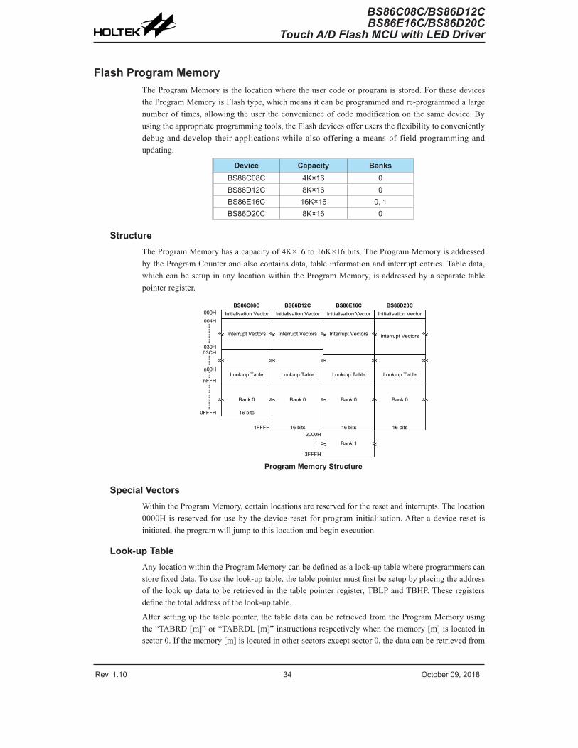
Rev. 1.10 34 October 09, 2018 Rev. 1.10 35 October 09, 2018
BS86C08C/BS86D12CBS86E16C/BS86D20C
Touch A/D Flash MCU with LED Driver
BS86C08C/BS86D12CBS86E16C/BS86D20CTouch A/D Flash MCU with LED Driver
Flash Program MemoryThe Program Memory is the location where the user code or program is stored. For these devices the Program Memory is Flash type, which means it can be programmed and re-programmed a large number of times, allowing the user the convenience of code modification on the same device. By using the appropriate programming tools, the Flash devices offer users the flexibility to conveniently debug and develop their applications while also offering a means of field programming and updating.
Device Capacity BanksBS86C08C 4K×16 0BS86D12C 8K×16 0BS86E16C 16K×16 0, 1BS86D20C 8K×16 0
StructureThe Program Memory has a capacity of 4K×16 to 16K×16 bits. The Program Memory is addressed by the Program Counter and also contains data, table information and interrupt entries. Table data, which can be setup in any location within the Program Memory, is addressed by a separate table pointer register.
Initialisation VectorBS86E16C BS86D20C
16 bits
Look-up Table
Initialisation Vector
16 bits
Interrupt Vectors
Look-up Table
BS86D12CInitialisation Vector
Bank 0
Interrupt Vectors
Look-up Table
BS86C08C000H004H
n00H
nFFH
0FFFH
1FFFH
030H
16 bits
03CH
Interrupt Vectors
Bank 0 Bank 0
Initialisation Vector
16 bits
Interrupt Vectors
Look-up Table
Bank 0
Bank 1
3FFFH
2000H
Program Memory Structure
Special VectorsWithin the Program Memory, certain locations are reserved for the reset and interrupts. The location 0000H is reserved for use by the device reset for program initialisation. After a device reset is initiated, the program will jump to this location and begin execution.
Look-up TableAny location within the Program Memory can be defined as a look-up table where programmers can store fixed data. To use the look-up table, the table pointer must first be setup by placing the address of the look up data to be retrieved in the table pointer register, TBLP and TBHP. These registers define the total address of the look-up table.
After setting up the table pointer, the table data can be retrieved from the Program Memory using the “TABRD [m]” or “TABRDL [m]” instructions respectively when the memory [m] is located in sector 0. If the memory [m] is located in other sectors except sector 0, the data can be retrieved from

Rev. 1.10 34 October 09, 2018 Rev. 1.10 35 October 09, 2018
BS86C08C/BS86D12CBS86E16C/BS86D20C
Touch A/D Flash MCU with LED Driver
BS86C08C/BS86D12CBS86E16C/BS86D20CTouch A/D Flash MCU with LED Driver
the program memory using the corresponding extended table read instruction such as “LTABRD [m]” or “LTABRDL [m]” respectively. When the instruction is executed, the lower order table byte from the Program Memory will be transferred to the user defined Data Memory register [m] as specified in the instruction. The higher order table data byte from the Program Memory will be transferred to the TBLH special register. Any unused bits in this transferred higher order byte will be read as “0”.
The accompanying diagram illustrates the addressing data flow of the look-up table.
Last Page or TBHP Register
Address
TBLP Register
Data16 bits
Program Memory
Register TBLH User Selected Register
High Byte Low Byte
Table Program ExampleThe following example shows how the table pointer and table data is defined and retrieved from the microcontroller. This example uses raw table data located in the Program Memory which is stored there using the ORG statement. The value at this ORG statement is “1F00H” which refers to the start address of the last page within the 8K Program Memory of the microcontroller. The table pointer low byte register is setup here to have an initial value of “06H”. This will ensure that the first data read from the data table will be at the Program Memory address “1F06H” or 6 locations after the start of the last page. Note that the value for the table pointer is referenced to the specific page pointed by the TBHP register if the “TABRD [m]” or “LTABRD [m]” instruction is being used. The high byte of the table data which in this case is equal to zero will be transferred to the TBLH register automatically when the “TABRD [m]” or “LTABRD [m]” instruction is executed.
Because the TBLH register is a read/write register and can be restored, care should be taken to ensure its protection if both the main routine and Interrupt Service Routine use table read instructions. If using the table read instructions, the Interrupt Service Routines may change the value of the TBLH and subsequently cause errors if used again by the main routine. As a rule it is recommended that simultaneous use of the table read instructions should be avoided. However, in situations where simultaneous use cannot be avoided, the interrupts should be disabled prior to the execution of any main routine table-read instructions. Note that all table related instructions require two instruction cycles to complete their operation.
Rev. 1.10 36 October 09, 2018 Rev. 1.10 37 October 09, 2018
BS86C08C/BS86D12CBS86E16C/BS86D20C
Touch A/D Flash MCU with LED Driver
BS86C08C/BS86D12CBS86E16C/BS86D20CTouch A/D Flash MCU with LED Driver
Table Read Program Exampletempreg1 db ? ; temporary register #1tempreg2 db ? ; temporary register #2::mov a,06h ; initialise low table pointer - note that this address ; is referencedmov tblp,a ; to the last page or the page that tbhp pointedmov a,1Fh ; initialise high table pointermov tbhp,a::tabrd tempreg1 ; transfers value in table referenced by table pointer data at program ; memory address “1F06H” transferred to tempreg1 and TBLHdec tblp ; reduce value of table pointer by onetabrd tempreg2 ; transfers value in table referenced by table pointer ; data at program memory address “1F05H” transferred to ; tempreg2 and TBLH ; in this example the data “1AH” is transferred to tempreg1 and data “0FH” ; to register tempreg2::org 1F00h ; sets initial address of program memorydc 00Ah, 00Bh, 00Ch, 00Dh, 00Eh, 00Fh, 01Ah, 01Bh::
In Circuit Programming – ICPThe provision of Flash type Program Memory provides the user with a means of convenient and easy upgrades and modifications to their programs on the same device.
As an additional convenience, Holtek has provided a means of programming the microcontroller in-circuit using a 4-pin interface. This provides manufacturers with the possibility of manufacturing their circuit boards complete with a programmed or un-programmed microcontroller, and then programming or upgrading the program at a later stage. This enables product manufacturers to easily keep their manufactured products supplied with the latest program releases without removal and re-insertion of the devices.
Holtek Writer Pins MCU Programming Pins Pin DescriptionICPDA PA0 Programming Serial Data/AddressICPCK PA2 Programming Clock
VDD VDD (BS86C08C/BS86D12C)VDD & VDDIO (BS86E16C/BS86D20C) Power Supply
VSS VSS Ground
The Program Memory can be programmed serially in-circuit using this 4-wire interface. Data is downloaded and uploaded serially on a single pin with an additional line for the clock. Two additional lines are required for the power supply. The technical details regarding the in-circuit programming of the devices is beyond the scope of this document and will be supplied in supplementary literature.
During the programming process, the user must take care of the ICPDA and ICPCK pins for data and clock programming purposes to ensure that no other outputs are connected to these two pins.

Rev. 1.10 36 October 09, 2018 Rev. 1.10 37 October 09, 2018
BS86C08C/BS86D12CBS86E16C/BS86D20C
Touch A/D Flash MCU with LED Driver
BS86C08C/BS86D12CBS86E16C/BS86D20CTouch A/D Flash MCU with LED Driver
*
Writer_VDD
ICPDA
ICPCK
Writer_VSS
To other Circuit
VDD
PA0
PA2
VSS
Writer Connector Signals
MCU ProgrammingPins
*
VDDIO **
Note: * may be resistor or capacitor. The resistance of * must be greater than 1kΩ or the capacitance of * must be less than 1nF. ** shows the VDDIO pin is only available for the BS86E16C/BS86D20C device.
On-Chip Debug Support – OCDSThere are EV chips named BS86CV08C, BS86DV12C, BS86EV16C and BS86DV20C which are used to emulate the real MCU devices named BS86C08C, BS86D12C, BS86E16C and BS86D20C respectively. The EV chip devices also provide an “On-Chip Debug” function to debug the real MCU devices during the development process. The EV chips and the real MCU devices are almost functionally compatible except for “On-Chip Debug” function. Users can use the EV chip device to emulate the real chip device behavior by connecting the OCDSDA and OCDSCK pins to the Holtek HT-IDE development tools. The OCDSDA pin is the OCDS Data/Address input/output pin while the OCDSCK pin is the OCDS clock input pin. When users use the EV chip device for debugging, the corresponding pin functions shared with the OCDSDA and OCDSCK pins in the real MCU device will have no effect in the EV chip. However, the two OCDS pins which are pin-shared with the ICP programming pins are still used as the Flash Memory programming pins for ICP. For more detailed OCDS information, refer to the corresponding document named “Holtek e-Link for 8-bit MCU OCDS User’s Guide”.
Holtek e-Link Pins EV Chip OCDS Pins Pin Description
OCDSDA OCDSDA On-Chip Debug Support Data/Address input/output
OCDSCK OCDSCK On-Chip Debug Support Clock input
VDD VDD (BS86CV08C/BS86DV12C)VDD & VDDIO (BS86EV16C/BS86DV20C) Power Supply
VSS VSS Ground

Rev. 1.10 38 October 09, 2018 Rev. 1.10 39 October 09, 2018
BS86C08C/BS86D12CBS86E16C/BS86D20C
Touch A/D Flash MCU with LED Driver
BS86C08C/BS86D12CBS86E16C/BS86D20CTouch A/D Flash MCU with LED Driver
Data MemoryThe Data Memory is a volatile area of 8-bit wide RAM internal memory and is the location where temporary information is stored.
Categorized into two types, the first of these is an area of RAM where special function registers are located. These registers have fixed locations and are necessary for correct operation of the devices. Many of these registers can be read from and written to directly under program control, however, some remain protected from user manipulation. The second area of Data Memory is reserved for general purpose use. All locations within this area are read and write accessible under program control.
Structure The overall Data Memory is subdivided into several sectors, all of which are implemented in 8-bit wide RAM. Each of the Data Memory Sector is categorized into two types, the special Purpose Data Memory and the General Purpose Data Memory. The address range of the Special Purpose Data Memory for the devices is from 00H to 7FH while the General Purpose Data Memory address range is from 80H to FFH. Switching between the different Data Memory sectors is achieved by setting the Memory Pointers to the correct value if using the indirect addressing method.
DeviceSpecial Purpose
Data MemoryGeneral Purpose
Data MemoryLocated Sectors Capacity Sector: Address
BS86C08C Sector 0, Sector 1 384×8Sector 0: 80H~FFHSector 1: 80H~FFHSector 2: 80H~FFH
BS86D12C Sector 0, Sector 1 512×8
Sector 0: 80H~FFHSector 1: 80H~FFHSector 2: 80H~FFHSector 3: 80H~FFH
BS86E16CBS86D20C Sector 0, Sector 1 768×8
Sector 0: 80H~FFHSector 1: 80H~FFHSector 2: 80H~FFHSector 3: 80H~FFHSector 4: 80H~FFHSector 5: 80H~FFH
Data Memory Summary
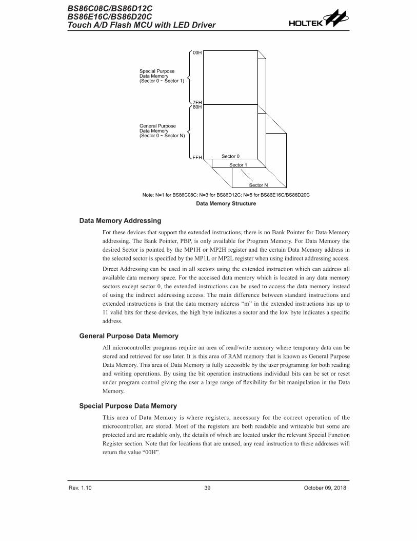
Rev. 1.10 38 October 09, 2018 Rev. 1.10 39 October 09, 2018
BS86C08C/BS86D12CBS86E16C/BS86D20C
Touch A/D Flash MCU with LED Driver
BS86C08C/BS86D12CBS86E16C/BS86D20CTouch A/D Flash MCU with LED Driver
Sector N
Sector 1
00H
7FH80H
FFH
Special Purpose Data Memory(Sector 0 ~ Sector 1)
General Purpose Data Memory(Sector 0 ~ Sector N)
Sector 0
Note: N=1 for BS86C08C; N=3 for BS86D12C; N=5 for BS86E16C/BS86D20C
Data Memory Structure
Data Memory AddressingFor these devices that support the extended instructions, there is no Bank Pointer for Data Memory addressing. The Bank Pointer, PBP, is only available for Program Memory. For Data Memory the desired Sector is pointed by the MP1H or MP2H register and the certain Data Memory address in the selected sector is specified by the MP1L or MP2L register when using indirect addressing access.
Direct Addressing can be used in all sectors using the extended instruction which can address all available data memory space. For the accessed data memory which is located in any data memory sectors except sector 0, the extended instructions can be used to access the data memory instead of using the indirect addressing access. The main difference between standard instructions and extended instructions is that the data memory address “m” in the extended instructions has up to 11 valid bits for these devices, the high byte indicates a sector and the low byte indicates a specific address.
General Purpose Data MemoryAll microcontroller programs require an area of read/write memory where temporary data can be stored and retrieved for use later. It is this area of RAM memory that is known as General Purpose Data Memory. This area of Data Memory is fully accessible by the user programing for both reading and writing operations. By using the bit operation instructions individual bits can be set or reset under program control giving the user a large range of flexibility for bit manipulation in the Data Memory.
Special Purpose Data MemoryThis area of Data Memory is where registers, necessary for the correct operation of the microcontroller, are stored. Most of the registers are both readable and writeable but some are protected and are readable only, the details of which are located under the relevant Special Function Register section. Note that for locations that are unused, any read instruction to these addresses will return the value “00H”.

Rev. 1.10 40 October 09, 2018 Rev. 1.10 41 October 09, 2018
BS86C08C/BS86D12CBS86E16C/BS86D20C
Touch A/D Flash MCU with LED Driver
BS86C08C/BS86D12CBS86E16C/BS86D20CTouch A/D Flash MCU with LED Driver
00H01H02H03H04H05H06H07H08H09H0AH0BH0CH0DH0EH0FH10H11H12H13H14H15H16H17H18H19H1AH1BH1CH1DH1EH1FH
Sector 0 Sector 1Sector 0EEC
Sector 1IAR0MP0IAR1MP1LMP1HACCPCLTBLPTBLH
STATUS
INTEGINTC0INTC1
PAPAC
PAPUPAWU
EEA
SLEDC0SLEDC1WDTCTBC
PSCRLVRC
TBHP
: Unused, read as 00H
40H41H42H43H44H45H46H47H48H49H4AH4BH4CH4DH4EH4FH50H51H52H53H54H55H56H57H58H59H5AH5BH5CH5DH5EH5FH
PDPU
20H21H22H23H24H25H26H27H28H29H2AH2BH2CH2DH2EH2FH30H31H32H33H34H35H36H37H38H39H3AH3BH3CH3DH3EH3FH
SADC0
60H61H62H63H64H65H66H67H68H69H6AH6BH6CH6DH6EH6FH70H71H72H73H74H75H76H77H78H79H7AH7BH7CH7DH7EH7FH
SMODIAR2MP2LMP2H
SADC1
IFS2
TMPCIFS0IFS1
ACERL
INTC2INTC3
TKTMR
PCC
PDC
CTRLPD
PCPU
U0CR1U0SR
EED
PBCPBPU
PB
SADOH
TXR_RXR0BRG0
SADOL
U0CR2
IICC0
IICDIICA
IICTOC
IICC1
PC
LVDC
TKM016DHTKM0ROLTKM0ROHTKM0C0TKM0C1
TKM016DL
TK16DLTK16DH
TKC1
TKC0
TKM116DHTKM1ROLTKM1ROHTKM1C0TKM1C1
TKM116DL
CTM0DL
CTM0C0CTM0C1
CTM0ALCTM0AH
CTM0DH
PTM0DL
PTM0RPH
PTM0C0PTM0C1
PTM0ALPTM0AH
PTM0RPL
PTM0DH
SLEDCOM1SLEDCOM2
SLEDCOM0
Special Purpose Data Memory Structure – BS86C08C

Rev. 1.10 40 October 09, 2018 Rev. 1.10 41 October 09, 2018
BS86C08C/BS86D12CBS86E16C/BS86D20C
Touch A/D Flash MCU with LED Driver
BS86C08C/BS86D12CBS86E16C/BS86D20CTouch A/D Flash MCU with LED Driver
00H01H02H03H04H05H06H07H08H09H0AH0BH0CH0DH0EH0FH10H11H12H13H14H15H16H17H18H19H1AH1BH1CH1DH1EH1FH
Sector 0 Sector 1Sector 0EEC
Sector 1IAR0MP0IAR1MP1LMP1HACCPCLTBLPTBLH
STATUS
INTEGINTC0INTC1
PAPAC
PAPUPAWU
EEA
SLEDC0SLEDC1WDTCTBC
PSCRLVRC
TBHP
: Unused, read as 00H
40H41H42H43H44H45H46H47H48H49H4AH4BH4CH4DH4EH4FH50H51H52H53H54H55H56H57H58H59H5AH5BH5CH5DH5EH5FH
PDPU
20H21H22H23H24H25H26H27H28H29H2AH2BH2CH2DH2EH2FH30H31H32H33H34H35H36H37H38H39H3AH3BH3CH3DH3EH3FH
SADC0
60H61H62H63H64H65H66H67H68H69H6AH6BH6CH6DH6EH6FH70H71H72H73H74H75H76H77H78H79H7AH7BH7CH7DH7EH7FH
SMODIAR2MP2LMP2H
SADC1
IFS2
TMPCIFS0IFS1
ACERL
INTC2INTC3
TKTMR
PCC
PDC
CTRLPD
PCPU
U0CR1U0SR
EED
PBCPBPU
PB
SADOH
TXR_RXR0BRG0
SADOL
U0CR2
IICC0
IICDIICA
IICTOC
IICC1
PC
LVDC
TKM016DHTKM0ROLTKM0ROHTKM0C0TKM0C1
TKM016DL
TK16DLTK16DH
TKC1
TKC0
TKM116DHTKM1ROLTKM1ROHTKM1C0TKM1C1
TKM116DL
TKM216DHTKM2ROLTKM2ROHTKM2C0TKM2C1
TKM216DL
CTM0DL
CTM0C0CTM0C1
CTM0ALCTM0AH
CTM0DH
PTM0DL
PTM0RPH
PTM0C0PTM0C1
PTM0ALPTM0AH
PTM0RPL
PTM0DH
SLEDCOM1SLEDCOM2
SLEDCOM0
Special Purpose Data Memory Structure – BS86D12C
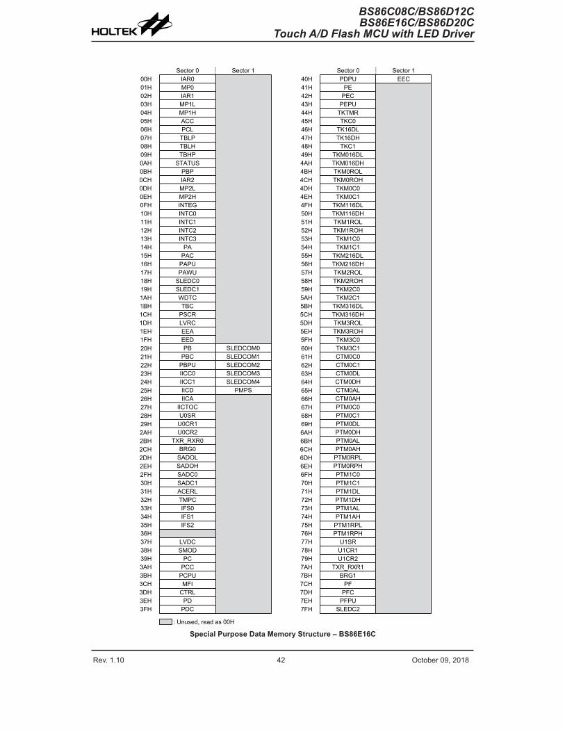
Rev. 1.10 42 October 09, 2018 Rev. 1.10 43 October 09, 2018
BS86C08C/BS86D12CBS86E16C/BS86D20C
Touch A/D Flash MCU with LED Driver
BS86C08C/BS86D12CBS86E16C/BS86D20CTouch A/D Flash MCU with LED Driver
00H01H02H03H04H05H06H07H08H09H0AH0BH0CH0DH0EH0FH10H11H12H13H14H15H16H17H18H19H1AH1BH1CH1DH1EH1FH
Sector 0 Sector 1Sector 0EEC
Sector 1IAR0MP0IAR1MP1LMP1HACCPCLTBLPTBLH
STATUS
INTEGINTC0INTC1
PAPAC
PAPUPAWU
EEA
SLEDC0SLEDC1WDTCTBC
PSCRLVRC
TBHP
: Unused, read as 00H
40H41H42H43H44H45H46H47H48H49H4AH4BH4CH4DH4EH4FH50H51H52H53H54H55H56H57H58H59H5AH5BH5CH5DH5EH5FH
PDPUPE
PEC
20H21H22H23H24H25H26H27H28H29H2AH2BH2CH2DH2EH2FH30H31H32H33H34H35H36H37H38H39H3AH3BH3CH3DH3EH3FH
SADC0
60H61H62H63H64H65H66H67H68H69H6AH6BH6CH6DH6EH6FH70H71H72H73H74H75H76H77H78H79H7AH7BH7CH7DH7EH7FH
PBPIAR2MP2LMP2H
SADC1
IFS2
TMPCIFS0IFS1
ACERL
INTC2INTC3
PEPUTKTMR
PCC
PDC
MFICTRL
PD
PCPU
U0CR1U0SR
EED
PBCPBPU
PB
SADOH
TXR_RXR0BRG0
SADOL
U0CR2
IICC0
IICDIICA
IICTOC
IICC1
SMODPC
LVDC
TKM016DHTKM0ROLTKM0ROHTKM0C0TKM0C1
TKM016DL
TK16DLTK16DH
TKC1
TKC0
TKM116DHTKM1ROLTKM1ROHTKM1C0TKM1C1
TKM116DL
TKM216DHTKM2ROLTKM2ROHTKM2C0TKM2C1
TKM216DL
TKM316DHTKM3ROLTKM3ROHTKM3C0TKM3C1
TKM316DL
U1CR1U1SR
TXR_RXR1BRG1
U1CR2
CTM0DL
CTM0C0CTM0C1
CTM0ALCTM0AH
CTM0DH
PTM0DL
PTM0RPH
PTM0C0PTM0C1
PTM0ALPTM0AH
PTM0RPL
PTM0DH
PTM1DL
PTM1RPH
PTM1C0PTM1C1
PTM1ALPTM1AH
PTM1RPL
PTM1DH
SLEDC2
PFPFC
PFPU
SLEDCOM1SLEDCOM2
SLEDCOM0
SLEDCOM3
PMPSSLEDCOM4
Special Purpose Data Memory Structure – BS86E16C

Rev. 1.10 42 October 09, 2018 Rev. 1.10 43 October 09, 2018
BS86C08C/BS86D12CBS86E16C/BS86D20C
Touch A/D Flash MCU with LED Driver
BS86C08C/BS86D12CBS86E16C/BS86D20CTouch A/D Flash MCU with LED Driver
00H01H02H03H04H05H06H07H08H09H0AH0BH0CH0DH0EH0FH10H11H12H13H14H15H16H17H18H19H1AH1BH1CH1DH1EH1FH
Sector 0 Sector 1Sector 0EEC
Sector 1IAR0MP0IAR1MP1LMP1HACCPCLTBLPTBLH
STATUS
INTEGINTC0INTC1
PAPAC
PAPUPAWU
EEA
SLEDC0SLEDC1WDTCTBC
PSCRLVRC
TBHP
: Unused, read as 00H
40H41H42H43H44H45H46H47H48H49H4AH4BH4CH4DH4EH4FH50H51H52H53H54H55H56H57H58H59H5AH5BH5CH5DH5EH5FH
PDPU
20H21H22H23H24H25H26H27H28H29H2AH2BH2CH2DH2EH2FH30H31H32H33H34H35H36H37H38H39H3AH3BH3CH3DH3EH3FH
SADC0
60H61H62H63H64H65H66H67H68H69H6AH6BH6CH6DH6EH6FH70H71H72H73H74H75H76H77H78H79H7AH7BH7CH7DH7EH7FH
IAR2MP2LMP2H
SADC1
TMPCIFS0IFS1
ACERL
INTC2INTC3
TKTMR
PCC
PDC
MFICTRL
PD
PCPU
U0CR1U0SR
EED
PBCPBPU
PB
SADOH
TXR_RXR0BRG0
SADOL
U0CR2
SIMTOC
SIMC1SIMD
SIMC2/SIMA
SIMC0
SMODPC
LVDC
TKM016DHTKM0ROLTKM0ROHTKM0C0TKM0C1
TKM016DL
TK16DLTK16DH
TKC1
TKC0
TKM116DHTKM1ROLTKM1ROHTKM1C0TKM1C1
TKM116DL
TKM216DHTKM2ROLTKM2ROHTKM2C0TKM2C1
TKM216DL
TKM316DHTKM3ROLTKM3ROHTKM3C0TKM3C1
TKM316DL
CTM0DL
CTM0C0CTM0C1
CTM0ALCTM0AH
CTM0DH
PTM0DL
PTM0RPH
PTM0C0PTM0C1
PTM0ALPTM0AH
PTM0RPL
PTM0DH
PTM1DL
PTM1RPH
PTM1C0PTM1C1
PTM1ALPTM1AH
PTM1RPL
PTM1DH
SLEDCOM1SLEDCOM2
SLEDCOM0
TKM416DHTKM4ROLTKM4ROHTKM4C0TKM4C1
TKM416DL
Special Purpose Data Memory Structure – BS86D20C

Rev. 1.10 44 October 09, 2018 Rev. 1.10 45 October 09, 2018
BS86C08C/BS86D12CBS86E16C/BS86D20C
Touch A/D Flash MCU with LED Driver
BS86C08C/BS86D12CBS86E16C/BS86D20CTouch A/D Flash MCU with LED Driver
Special Function Register DescriptionMost of the Special Function Register details will be described in the relevant functional sections. However, several registers require a separate description in this section.
Indirect Addressing Registers – IAR0, IAR1, IAR2The Indirect Addressing Registers, IAR0, IAR1 and IAR2, although having their locations in normal RAM register space, do not actually physically exist as normal registers. The method of indirect addressing for RAM data manipulation uses these Indirect Addressing Registers and Memory Pointers, in contrast to direct memory addressing, where the actual memory address is specified. Actions on the IAR0, IAR1 and IAR2 registers will result in no actual read or write operation to these registers but rather to the memory location specified by their corresponding Memory Pointers, MP0, MP1L/MP1H or MP2L/MP2H. Acting as a pair, IAR0 and MP0 can together access data only from Sector 0 while the IAR1 register together with the MP1L/MP1H register pair and IAR2 register together with the MP2L/MP2H register pair can access data from any Data Memory Sector. As the Indirect Addressing Registers are not physically implemented, reading the Indirect Addressing Registers will return a result of “00H” and writing to the registers will result in no operation.
Memory Pointers – MP0, MP1L, MP1H, MP2L, MP2HFive Memory Pointers, known as MP0, MP1L, MP1H, MP2L, MP2H, are provided. These Memory Pointers are physically implemented in the Data Memory and can be manipulated in the same way as normal registers providing a convenient way with which to address and track data. When any operation to the relevant Indirect Addressing Registers is carried out, the actual address that the microcontroller is directed to is the address specified by the related Memory Pointer. MP0, together with Indirect Addressing Register, IAR0, are used to access data from Sector 0, while MP1L/MP1H together with IAR1 and MP2L/MP2H together with IAR2 are used to access data from all sectors according to the corresponding MP1H or MP2H register. Direct Addressing can be used in all sectors using the extended instruction which can address all available Data Memory space.
The following example shows how to clear a section of four Data Memory locations already defined as locations adres1 to adres4.
Indirect Addressing Program Example 1data .section ´data´adres1 db ?adres2 db ?adres3 db ?adres4 db ?block db ?code .section at 0 code´org 00hstart: mov a, 04h ; setup size of block mov block, a mova,offsetadres1 ;AccumulatorloadedwithfirstRAMaddress movmp0,a ;setupmemorypointerwithfirstRAMaddressloop: clrIAR0 ;clearthedataataddressdefinedbyMP0 inc mp0 ; increment memory pointer sdz block ; check if last memory location has been cleared jmp loopcontinue:
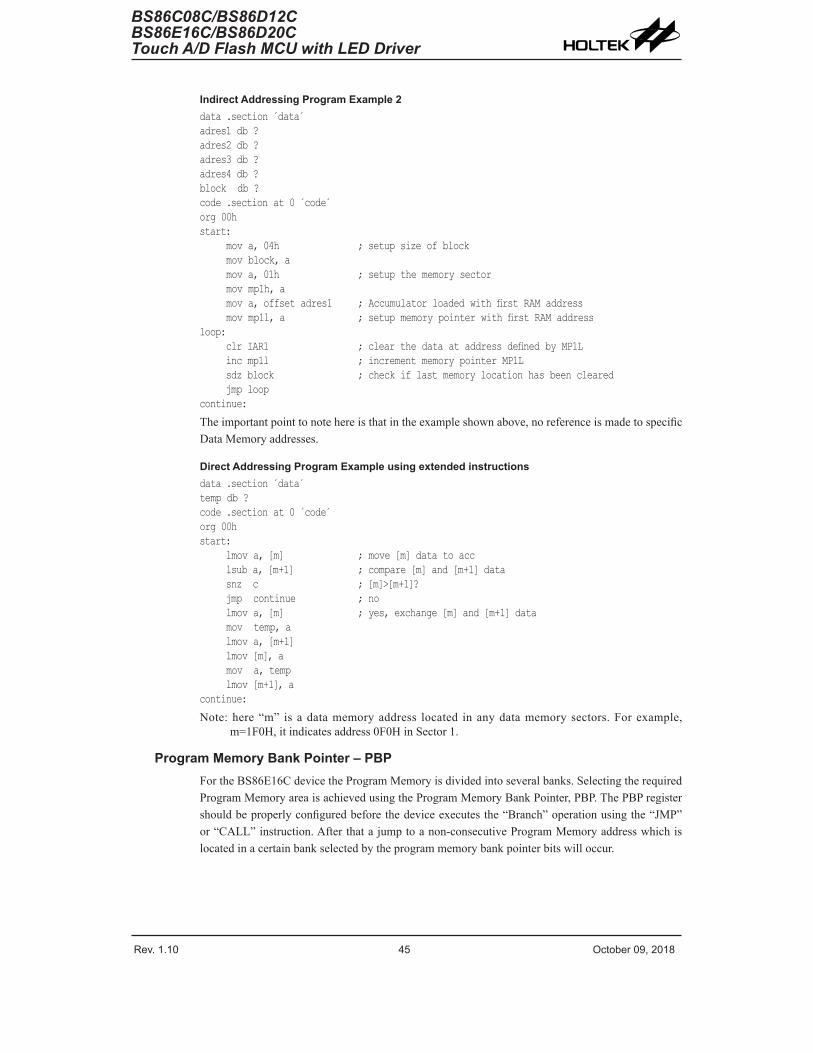
Rev. 1.10 44 October 09, 2018 Rev. 1.10 45 October 09, 2018
BS86C08C/BS86D12CBS86E16C/BS86D20C
Touch A/D Flash MCU with LED Driver
BS86C08C/BS86D12CBS86E16C/BS86D20CTouch A/D Flash MCU with LED Driver
Indirect Addressing Program Example 2data .section ´data´adres1 db ?adres2 db ?adres3 db ?adres4 db ?block db ?code .section at 0 code´org 00hstart: mov a, 04h ; setup size of block mov block, a mov a, 01h ; setup the memory sector mov mp1h, a mova,offsetadres1 ;AccumulatorloadedwithfirstRAMaddress movmp1l,a ;setupmemorypointerwithfirstRAMaddressloop: clrIAR1 ;clearthedataataddressdefinedbyMP1L incmp1l ;incrementmemorypointerMP1L sdz block ; check if last memory location has been cleared jmp loopcontinue:
The important point to note here is that in the example shown above, no reference is made to specific Data Memory addresses.
Direct Addressing Program Example using extended instructionsdata .section ´data´temp db ?code .section at 0 code´org 00hstart: lmov a, [m] ; move [m] data to acc lsub a, [m+1] ; compare [m] and [m+1] data snz c ; [m]>[m+1]? jmp continue ; no lmov a, [m] ; yes, exchange [m] and [m+1] data mov temp, a lmov a, [m+1] lmov [m], a mov a, temp lmov [m+1], acontinue:
Note: here “m” is a data memory address located in any data memory sectors. For example, m=1F0H, it indicates address 0F0H in Sector 1.
Program Memory Bank Pointer – PBPFor the BS86E16C device the Program Memory is divided into several banks. Selecting the required Program Memory area is achieved using the Program Memory Bank Pointer, PBP. The PBP register should be properly configured before the device executes the “Branch” operation using the “JMP” or “CALL” instruction. After that a jump to a non-consecutive Program Memory address which is located in a certain bank selected by the program memory bank pointer bits will occur.

Rev. 1.10 46 October 09, 2018 Rev. 1.10 47 October 09, 2018
BS86C08C/BS86D12CBS86E16C/BS86D20C
Touch A/D Flash MCU with LED Driver
BS86C08C/BS86D12CBS86E16C/BS86D20CTouch A/D Flash MCU with LED Driver
• PBP Register – BS86E16C
Bit 7 6 5 4 3 2 1 0Name — — — — — — — PBP0R/W — — — — — — — R/WPOR — — — — — — — 0
Bit 7~1 Unimplemented, read as “0”Bit 0 PBP0: Select Program Memory Bank
0: Bank 01: Bank 1
Accumulator – ACC The Accumulator is central to the operation of any microcontroller and is closely related with operations carried out by the ALU. The Accumulator is the place where all intermediate results from the ALU are stored. Without the Accumulator it would be necessary to write the result of each calculation or logical operation such as addition, subtraction, shift, etc., to the Data Memory resulting in higher programming and timing overheads. Data transfer operations usually involve the temporary storage function of the Accumulator; for example, when transferring data between one user-defined register and another, it is necessary to do this by passing the data through the Accumulator as no direct transfer between two registers is permitted.
Program Counter Low Register – PCL To provide additional program control functions, the low byte of the Program Counter is made accessible to programmers by locating it within the Special Purpose area of the Data Memory. By manipulating this register, direct jumps to other program locations are easily implemented. Loading a value directly into this PCL register will cause a jump to the specified Program Memory location, however, as the register is only 8-bit wide, only jumps within the current Program Memory page are permitted. When such operations are used, note that a dummy cycle will be inserted.
Look-up Table Registers – TBLP, TBHP, TBLH These three special function registers are used to control operation of the look-up table which is stored in the Program Memory. TBLP and TBHP are the table pointers and indicate the location where the table data is located. Their value must be setup before any table read commands are executed. Their value can be changed, for example using the “INC” or “DEC” instructions, allowing for easy table data pointing and reading. TBLH is the location where the high order byte of the table data is stored after a table read data instruction has been executed. Note that the lower order table data byte is transferred to a user defined location.
Status Register – STATUS This 8-bit register contains the SC flag, CZ flag, zero flag (Z), carry flag (C), auxiliary carry flag (AC), overflow flag (OV), power down flag (PDF), and watchdog time-out flag (TO). These arithmetic/logical operation and system management flags are used to record the status and operation of the microcontroller.
With the exception of the TO and PDF flags, bits in the status register can be altered by instructions like most other registers. Any data written into the status register will not change the TO or PDF flag. In addition, operations related to the status register may give different results due to the different instruction operations. The TO flag can be affected only by a system power-up, a WDT time-out or by executing the “CLR WDT” or “HALT” instruction. The PDF flag is affected only by executing the “HALT” or “CLR WDT” instruction or during a system power-up.

Rev. 1.10 46 October 09, 2018 Rev. 1.10 47 October 09, 2018
BS86C08C/BS86D12CBS86E16C/BS86D20C
Touch A/D Flash MCU with LED Driver
BS86C08C/BS86D12CBS86E16C/BS86D20CTouch A/D Flash MCU with LED Driver
The Z, OV, AC, C, SC and CZ flags generally reflect the status of the latest operations.
• C is set if an operation results in a carry during an addition operation or if a borrow does not take place during a subtraction operation; otherwise C is cleared. C is also affected by a rotate through carry instruction.
• AC is set if an operation results in a carry out of the low nibbles in addition, or no borrow from the high nibble into the low nibble in subtraction; otherwise AC is cleared.
• Z is set if the result of an arithmetic or logical operation is zero; otherwise Z is cleared.
• OV is set if an operation results in a carry into the highest-order bit but not a carry out of the highest-order bit, or vice versa; otherwise OV is cleared.
• PDF is cleared by a system power-up or executing the “CLR WDT” instruction. PDF is set by executing the “HALT” instruction.
• TO is cleared by a system power-up or executing the “CLR WDT” or “HALT” instruction. TO is set by a WDT time-out.
• CZ is the operational result of different flags for different instructions. Refer to register definitions for more details.
• SC is the result of the “XOR” operation which is performed by the OV flag and the MSB of the current instruction operation result.
In addition, on entering an interrupt sequence or executing a subroutine call, the status register will not be pushed onto the stack automatically. If the contents of the status registers are important and if the subroutine can corrupt the status register, precautions must be taken to correctly save it.
• STATUS Register
Bit 7 6 5 4 3 2 1 0Name SC CZ TO PDF OV Z AC CR/W R/W R/W R R R/W R/W R/W R/WPOR x x 0 0 x x x x
“x”: unknownBit 7 SC: The result of the “XOR” operation which is performed by the OV flag and the
MSB of the instruction operation result.Bit 6 CZ: The operational result of different flags for different instructions.
For SUB/SUBM/LSUB/LSUBM instructions, the CZ flag is equal to the Z flag. For SBC/SBCM/LSBC/LSBCM instructions, the CZ flag is the “AND” operation result which is performed by the previous operation CZ flag and current operation zero flag. For other instructions, the CZ flag will not be affected.
Bit 5 TO: Watchdog Time-out flag0: After power up or executing the “CLR WDT” or “HALT” instruction1: A watchdog time-out occurred.
Bit 4 PDF: Power down flag0: After power up or executing the “CLR WDT” instruction1: By executing the “HALT” instruction
Bit 3 OV: Overflow flag0: No overflow1: An operation results in a carry into the highest-order bit but not a carry out of the
highest-order bit or vice versa.Bit 2 Z: Zero flag
0: The result of an arithmetic or logical operation is not zero1: The result of an arithmetic or logical operation is zero
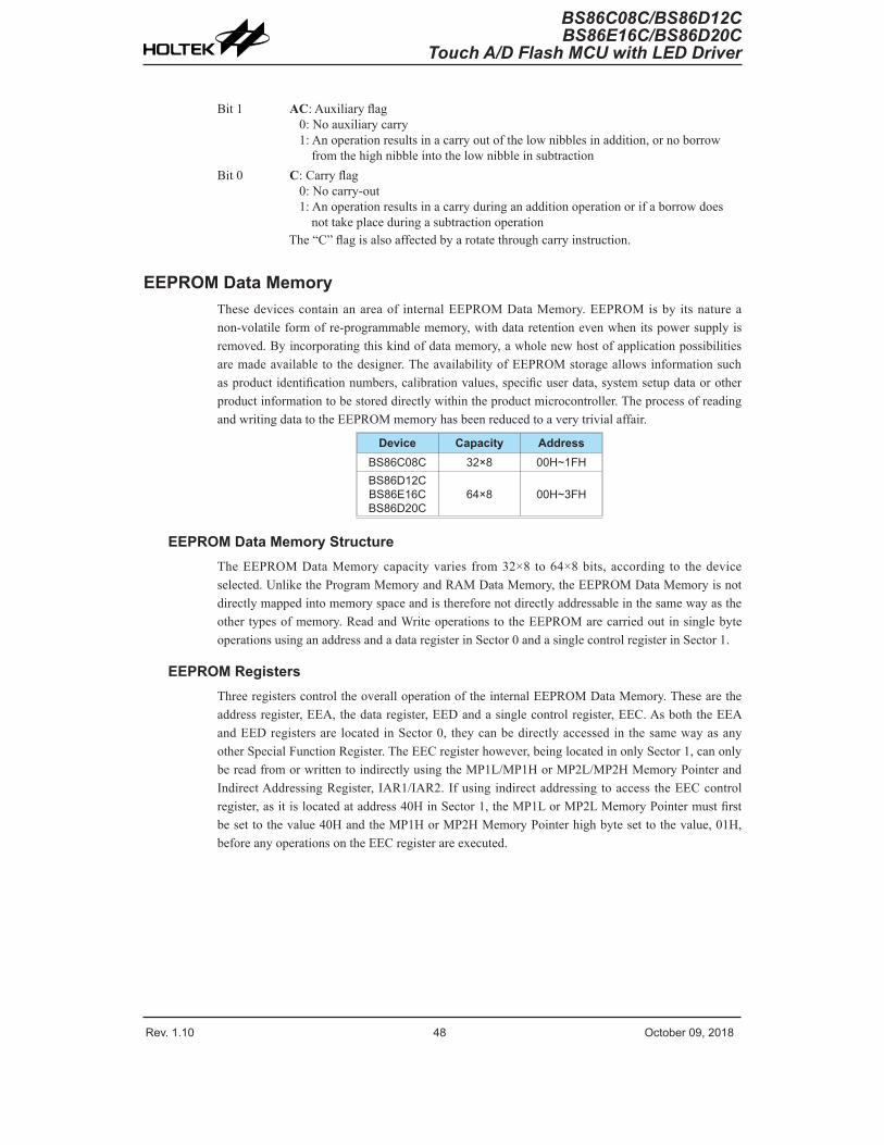
Rev. 1.10 48 October 09, 2018 Rev. 1.10 49 October 09, 2018
BS86C08C/BS86D12CBS86E16C/BS86D20C
Touch A/D Flash MCU with LED Driver
BS86C08C/BS86D12CBS86E16C/BS86D20CTouch A/D Flash MCU with LED Driver
Bit 1 AC: Auxiliary flag0: No auxiliary carry1: An operation results in a carry out of the low nibbles in addition, or no borrow
from the high nibble into the low nibble in subtractionBit 0 C: Carry flag
0: No carry-out1: An operation results in a carry during an addition operation or if a borrow does
not take place during a subtraction operationThe “C” flag is also affected by a rotate through carry instruction.
EEPROM Data MemoryThese devices contain an area of internal EEPROM Data Memory. EEPROM is by its nature a non-volatile form of re-programmable memory, with data retention even when its power supply is removed. By incorporating this kind of data memory, a whole new host of application possibilities are made available to the designer. The availability of EEPROM storage allows information such as product identification numbers, calibration values, specific user data, system setup data or other product information to be stored directly within the product microcontroller. The process of reading and writing data to the EEPROM memory has been reduced to a very trivial affair.
Device Capacity AddressBS86C08C 32×8 00H~1FHBS86D12CBS86E16CBS86D20C
64×8 00H~3FH
EEPROM Data Memory StructureThe EEPROM Data Memory capacity varies from 32×8 to 64×8 bits, according to the device selected. Unlike the Program Memory and RAM Data Memory, the EEPROM Data Memory is not directly mapped into memory space and is therefore not directly addressable in the same way as the other types of memory. Read and Write operations to the EEPROM are carried out in single byte operations using an address and a data register in Sector 0 and a single control register in Sector 1.
EEPROM RegistersThree registers control the overall operation of the internal EEPROM Data Memory. These are the address register, EEA, the data register, EED and a single control register, EEC. As both the EEA and EED registers are located in Sector 0, they can be directly accessed in the same way as any other Special Function Register. The EEC register however, being located in only Sector 1, can only be read from or written to indirectly using the MP1L/MP1H or MP2L/MP2H Memory Pointer and Indirect Addressing Register, IAR1/IAR2. If using indirect addressing to access the EEC control register, as it is located at address 40H in Sector 1, the MP1L or MP2L Memory Pointer must first be set to the value 40H and the MP1H or MP2H Memory Pointer high byte set to the value, 01H, before any operations on the EEC register are executed.

Rev. 1.10 48 October 09, 2018 Rev. 1.10 49 October 09, 2018
BS86C08C/BS86D12CBS86E16C/BS86D20C
Touch A/D Flash MCU with LED Driver
BS86C08C/BS86D12CBS86E16C/BS86D20CTouch A/D Flash MCU with LED Driver
Register Name
Bit
7 6 5 4 3 2 1 0EEA(BS86C08C) — — — EEA4 EEA3 EEA2 EEA1 EEA0
EEA(BS86D12C/BS86E16C/BS86D20C)
— — EEA5 EEA4 EEA3 EEA2 EEA1 EEA0
EED D7 D6 D5 D4 D3 D2 D1 D0EEC — — — — WREN WR RDEN RD
EEPROM Register List
• EEA Register – BS86C08C
Bit 7 6 5 4 3 2 1 0Name — — — EEA4 EEA3 EEA2 EEA1 EEA0R/W — — — R/W R/W R/W R/W R/WPOR — — — 0 0 0 0 0
Bit 7~5 Unimplemented, read as “0”Bit 4~0 EEA4~EEA0: Data EEPROM address bit 4~bit 0
• EEA Register – BS86D12C/BS86E16C/BS86D20C
Bit 7 6 5 4 3 2 1 0Name — — EEA5 EEA4 EEA3 EEA2 EEA1 EEA0R/W — — R/W R/W R/W R/W R/W R/WPOR — — 0 0 0 0 0 0
Bit 7~6 Unimplemented, read as “0”Bit 5~0 EEA5~EEA0: Data EEPROM address bit 5~bit 0
• EED Register
Bit 7 6 5 4 3 2 1 0Name D7 D6 D5 D4 D3 D2 D1 D0R/W R/W R/W R/W R/W R/W R/W R/W R/WPOR 0 0 0 0 0 0 0 0
Bit 7~0 D7~D0: Data EEPROM data bit 7~bit 0
• EEC Register
Bit 7 6 5 4 3 2 1 0Name — — — — WREN WR RDEN RDR/W — — — — R/W R/W R/W R/WPOR — — — — 0 0 0 0
Bit 7~4 Unimplemented, read as “0”Bit 3 WREN: Data EEPROM Write Enable
0: Disable1: Enable
This is the Data EEPROM Write Enable Bit which must be set high before Data EEPROM write operations are carried out. Clearing this bit to zero will inhibit Data EEPROM write operations.

Rev. 1.10 50 October 09, 2018 Rev. 1.10 51 October 09, 2018
BS86C08C/BS86D12CBS86E16C/BS86D20C
Touch A/D Flash MCU with LED Driver
BS86C08C/BS86D12CBS86E16C/BS86D20CTouch A/D Flash MCU with LED Driver
Bit 2 WR: EEPROM Write Control0: Write cycle has finished1: Activate a write cycle
This is the Data EEPROM Write Control Bit and when set high by the application program will activate a write cycle. This bit will be automatically reset to zero by the hardware after the write cycle has finished. Setting this bit high will have no effect if the WREN has not first been set high.
Bit 1 RDEN: Data EEPROM Read Enable0: Disable1: Enable
This is the Data EEPROM Read Enable Bit which must be set high before Data EEPROM read operations are carried out. Clearing this bit to zero will inhibit Data EEPROM read operations.
Bit 0 RD: EEPROM Read Control0: Read cycle has finished1: Activate a read cycle
This is the Data EEPROM Read Control Bit and when set high by the application program will activate a read cycle. This bit will be automatically reset to zero by the hardware after the read cycle has finished. Setting this bit high will have no effect if the RDEN has not first been set high.
Note: 1. The WREN, WR, RDEN and RD cannot be set high at the same time in one instruction. The WR and RD cannot be set high at the same time.
2. Ensure that the fSUB clock is stable before executing the write operation. 3. Ensure that the write operation is totally complete before changing the EEC register content.
Reading Data from the EEPROMTo read data from the EEPROM, the EEPROM address of the data to be read must first be placed in the EEA register. The read enable bit, RDEN, in the EEC register must then be set high to enable the read function. If the RD bit in the EEC register is now set high, a read cycle will be initiated. Setting the RD bit high will not initiate a read operation if the RDEN bit has not been set. When the read cycle terminates, the RD bit will be automatically cleared to zero, after which the data can be read from the EED register. The data will remain in the EED register until another read or write operation is executed. The application program can poll the RD bit to determine when the data is valid for reading.
Writing Data to the EEPROMTo write data to the EEPROM, the EEPROM address of the data to be written must first be placed in the EEA register and the data placed in the EED register. To initiate a write cycle the write enable bit, WREN, in the EEC register must first be set high to enable the write function. After this, the WR bit in the EEC register must be immediately set high to initiate a write cycle successfully. These two instructions must be executed in two consecutive instruction cycles. The global interrupt bit EMI should also first be cleared before implementing any write operations, and then set high again after the write cycle has started. Note that setting the WR bit high will not initiate a write cycle if the WREN bit has not been set. As the EEPROM write cycle is controlled using an internal timer whose operation is asynchronous to microcontroller system clock, a certain time will elapse before the data will have been written into the EEPROM. Detecting when the write cycle has finished can be implemented either by polling the WR bit in the EEC register or by using the EEPROM interrupt. When the write cycle terminates, the WR bit will be automatically cleared to zero by the microcontroller, informing the user that the data has been written to the EEPROM. The application program can therefore poll the WR bit to determine when the write cycle has ended.

Rev. 1.10 50 October 09, 2018 Rev. 1.10 51 October 09, 2018
BS86C08C/BS86D12CBS86E16C/BS86D20C
Touch A/D Flash MCU with LED Driver
BS86C08C/BS86D12CBS86E16C/BS86D20CTouch A/D Flash MCU with LED Driver
Write ProtectionProtection against inadvertent write operation is provided in several ways. After these devices are powered-on the Write Enable bit in the control register will be cleared preventing any write operations. Also at power-on the Memory Pointer high byte register, MP1H or MP2H, will be reset to zero, which means that Data Memory Sector 0 will be selected. As the EEPROM control register is located in Sector 1, this adds a further measure of protection against spurious write operations. During normal program operation, ensuring that the Write Enable bit in the control register is cleared will safeguard against incorrect write operations.
EEPROM InterruptThe EEPROM write interrupt is generated when an EEPROM write cycle has ended. The EEPROM interrupt must first be enabled by setting the DEE bit in the relevant interrupt register. When an EEPROM write cycle ends, the DEF request flag will be set. If the global, EEPROM interrupts are enabled and the stack is not full, a jump to the associated EEPROM Interrupt vector will take place. When the interrupt is serviced, the EEPROM Interrupt flag, DEF, will be automatically cleared. The EMI bit will also be automatically cleared to disable other interrupts. More details can be obtained in the Interrupt section.
Programming ConsiderationsCare must be taken that data is not inadvertently written to the EEPROM. Protection can be enhanced by ensuring that the Write Enable bit is normally cleared to zero when not writing. Also the Memory Pointer high byte register, MP1H or MP2H, could be normally cleared to zero as this would inhibit access to Sector 1 where the EEPROM control register exists. Although certainly not necessary, consideration might be given in the application program to the checking of the validity of new write data by a simple read back process.
When writing data the WR bit must be set high immediately after the WREN bit has been set high, to ensure the write cycle executes correctly. The global interrupt bit EMI should also be cleared before a write cycle is executed and then re-enabled after the write cycle starts. Note that these devices should not enter the IDLE or SLEEP mode until the EEPROM read or write operation is totally complete. Otherwise, the EEPROM read or write operation will fail.
Programming Examples
Reading data from the EEPROM – polling methodMOV A,EEPROM_ADRES ;userdefinedaddressMOV EEA,AMOV A,040H ;setupmemorypointerMP1LMOV MP1L,A ;MP1LpointstoEECregisterMOV A,01H ;setupmemorypointerMP1HMOV MP1H,ASET IAR1.1 ;setRDENbit,enablereadoperationsSET IAR1.0 ;startReadCycle-setRDbitBACK:SZ IAR1.0 ;checkforreadcycleendJMP BACKCLR IAR1 ;disableEEPROMreadifnomorereadoperationsarerequiredCLR MP1HMOV A,EED ;movereaddatatoregisterMOV READ_DATA,A
Note: For each read operation, the address register should be re-specified followed by setting the RD bit high to activate a read cycle even if the target address is consecutive.

Rev. 1.10 52 October 09, 2018 Rev. 1.10 53 October 09, 2018
BS86C08C/BS86D12CBS86E16C/BS86D20C
Touch A/D Flash MCU with LED Driver
BS86C08C/BS86D12CBS86E16C/BS86D20CTouch A/D Flash MCU with LED Driver
Writing Data to the EEPROM – polling methodMOV A,EEPROM_ADRES ;userdefinedaddressMOV EEA,AMOV A,EEPROM_DATA ;userdefineddataMOV EED,AMOV A,040H ;setupmemorypointerMP1LMOV MP1L,A ;MP1LpointstoEECregisterMOV A,01H ;setupmemorypointerMP1HMOV MP1H,ACLR EMISET IAR1.3 ;setWRENbit,enablewriteoperationsSET IAR1.2 ;startWriteCycle-setWRbit–executedimmediately ;aftersetWRENbitSET EMIBACK:SZ IAR1.2 ;checkforwritecycleendJMP BACKCLR MP1H
OscillatorsVarious oscillator types offer the user a wide range of functions according to their various application requirements. The flexible features of the oscillator functions ensure that the best optimisation can be achieved in terms of speed and power saving. Oscillator selections and operation are selected through a combination of configuration options and relevant control registers.
Oscillator OverviewIn addition to being the source of the main system clock the oscillators also provide clock sources for the Watchdog Timer and Time Base Interrupts. External oscillators requiring some external components as well as fully integrated internal oscillators, requiring no external components, are provided to form a wide range of both fast and slow system oscillators. The higher frequency oscillators provide higher performance but carry with it the disadvantage of higher power requirements, while the opposite is of course true for the lower frequency oscillators. With the capability of dynamically switching between fast and slow system clock, the device has the flexibility to optimize the performance/power ratio, a feature especially important in power sensitive portable applications.
Type Name Frequency PinsInternal High Speed RC HIRC 8/12/16MHz —Internal Low Speed RC LIRC 32kHz —External Low Speed Crystal (Note) LXT 32.768kHz XT1/XT2
Note: The external low speed crystal oscillator, LXT, is only available for the BS86E16C/BS86D20C device.
Oscillator Types
System Clock ConfigurationsThere are three methods of generating the system clock, one high speed oscillator and two low speed oscillators. The high speed oscillator is the internal 8/12/16MHz RC oscillator, HIRC. The two low speed oscillators are the internal 32kHz RC oscillator, LIRC, and the external 32.768kHz crystal oscillator, LXT. Selecting whether the low or high speed oscillator is used as the system oscillator is implemented using the HLCLK and CKS2~CKS0 bits in the SMOD register and as the system clock can be dynamically selected.

Rev. 1.10 52 October 09, 2018 Rev. 1.10 53 October 09, 2018
BS86C08C/BS86D12CBS86E16C/BS86D20C
Touch A/D Flash MCU with LED Driver
BS86C08C/BS86D12CBS86E16C/BS86D20CTouch A/D Flash MCU with LED Driver
The actual source clock used for the low speed oscillators is chosen via the corresponding configuration option. The frequency of the slow speed or high speed system clock is determined using the HLCLK and CKS2~CKS0 bits in the SMOD register. Note that two oscillator selections must be made namely one high speed and one low speed system oscillators. It is not possible to choose a no-oscillator selection for either the high or low speed oscillator.
Prescaler
LIRC
High Speed Oscillator
Low Speed Oscillator
fH/2
fH/16
fH/64
fH/8
fH/4
fH/32
HLCLK,CKS2~CKS0 bits
fSYS
fSUBfSUB
ConfigurationOption
LXT *
fLIRC
HIRC
fH
fLXT
Note: The LXT oscillator is only available for the BS86E16C/BS86D20C device.System Clock Configurations
Internal High Speed RC Oscillator – HIRCThe internal RC oscillator is a fully integrated system oscillator requiring no external components. The internal RC oscillator has three fixed frequencies of 8MHz, 12MHz and 16MHz, which is selected using a configuration option. The HIRCS1~HIRCS0 bits in the CTRL register must also be setup to match the selected configuration option frequency. Setting up these bits is necessary to ensure that the HIRC frequency accuracy specified in the A.C. Characteristics is achieved. Device trimming during the manufacturing process and the inclusion of internal frequency compensation circuits are used to ensure that the influence of the power supply voltage, temperature and process variations on the oscillation frequency are minimised. Note that if this internal system clock option is selected, as it requires no external pins for its operation, I/O pins are free for use as normal I/O pins.
Internal 32kHz Oscillator – LIRCThe Internal 32kHz System Oscillator is one of the low frequency oscillator choices, which is selected via a configuration option for the BS86E16C/BS86D20C device. For the BS86C08C/BS86D12C device there is only one low frequency oscillator known as the LIRC oscillator. It is a fully integrated RC oscillator with a typical frequency of 32kHz, requiring no external components for its implementation. Device trimming during the manufacturing process and the inclusion of internal frequency compensation circuits are used to ensure that the influence of the power supply voltage, temperature and process variations on the oscillation frequency are minimised.
External 32.768kHz Crystal Oscillator – LXT (BS86E16C/BS86D20C)The External 32.768kHz Crystal System Oscillator is one of the low frequency oscillator choices, which is selected via a configuration option. This clock source has a fixed frequency of 32.768kHz
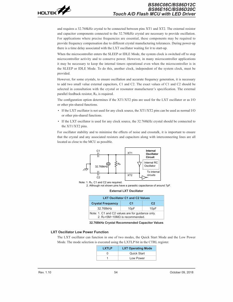
Rev. 1.10 54 October 09, 2018 Rev. 1.10 55 October 09, 2018
BS86C08C/BS86D12CBS86E16C/BS86D20C
Touch A/D Flash MCU with LED Driver
BS86C08C/BS86D12CBS86E16C/BS86D20CTouch A/D Flash MCU with LED Driver
and requires a 32.768kHz crystal to be connected between pins XT1 and XT2. The external resistor and capacitor components connected to the 32.768kHz crystal are necessary to provide oscillation. For applications where precise frequencies are essential, these components may be required to provide frequency compensation due to different crystal manufacturing tolerances. During power-up there is a time delay associated with the LXT oscillator waiting for it to start-up.
When the microcontroller enters the SLEEP or IDLE Mode, the system clock is switched off to stop microcontroller activity and to conserve power. However, in many microcontroller applications it may be necessary to keep the internal timers operational even when the microcontroller is in the SLEEP or IDLE Mode. To do this, another clock, independent of the system clock, must be provided.
However, for some crystals, to ensure oscillation and accurate frequency generation, it is necessary to add two small value external capacitors, C1 and C2. The exact values of C1 and C2 should be selected in consultation with the crystal or resonator manufacturer’s specification. The external parallel feedback resistor, RP, is required.
The configuration option determines if the XT1/XT2 pins are used for the LXT oscillator or as I/O or other pin-shared functions.
• If the LXT oscillator is not used for any clock source, the XT1/XT2 pins can be used as normal I/O or other pin-shared functions.
• If the LXT oscillator is used for any clock source, the 32.768kHz crystal should be connected to the XT1/XT2 pins.
For oscillator stability and to minimise the effects of noise and crosstalk, it is important to ensure that the crystal and any associated resistors and capacitors along with interconnecting lines are all located as close to the MCU as possible.
Note: 1. RP, C1 and C2 are required.2. Although not shown pins have a parasitic capacitance of around 7pF.
To internal circuits
Internal Oscillator Circuit
C1
C2
XT1
XT2
RP32.768kHz
Internal RC Oscillator
External LXT Oscillator
LXT Oscillator C1 and C2 Values
Crystal Frequency C1 C232.768kHz 10pF 10pF
Note: 1. C1 and C2 values are for guidance only.2. RP=5M~10MΩ is recommended.
32.768kHz Crystal Recommended Capacitor Values
LXT Oscillator Low Power FunctionThe LXT oscillator can function in one of two modes, the Quick Start Mode and the Low Power Mode. The mode selection is executed using the LXTLP bit in the CTRL register.
LXTLP LXT Operating Mode0 Quick Start1 Low Power
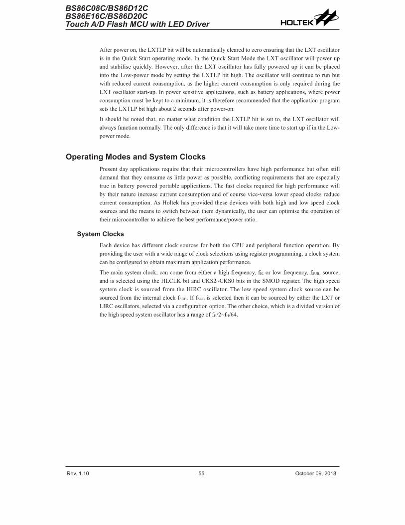
Rev. 1.10 54 October 09, 2018 Rev. 1.10 55 October 09, 2018
BS86C08C/BS86D12CBS86E16C/BS86D20C
Touch A/D Flash MCU with LED Driver
BS86C08C/BS86D12CBS86E16C/BS86D20CTouch A/D Flash MCU with LED Driver
After power on, the LXTLP bit will be automatically cleared to zero ensuring that the LXT oscillator is in the Quick Start operating mode. In the Quick Start Mode the LXT oscillator will power up and stabilise quickly. However, after the LXT oscillator has fully powered up it can be placed into the Low-power mode by setting the LXTLP bit high. The oscillator will continue to run but with reduced current consumption, as the higher current consumption is only required during the LXT oscillator start-up. In power sensitive applications, such as battery applications, where power consumption must be kept to a minimum, it is therefore recommended that the application program sets the LXTLP bit high about 2 seconds after power-on.
It should be noted that, no matter what condition the LXTLP bit is set to, the LXT oscillator will always function normally. The only difference is that it will take more time to start up if in the Low-power mode.
Operating Modes and System ClocksPresent day applications require that their microcontrollers have high performance but often still demand that they consume as little power as possible, conflicting requirements that are especially true in battery powered portable applications. The fast clocks required for high performance will by their nature increase current consumption and of course vice-versa lower speed clocks reduce current consumption. As Holtek has provided these devices with both high and low speed clock sources and the means to switch between them dynamically, the user can optimise the operation of their microcontroller to achieve the best performance/power ratio.
System ClocksEach device has different clock sources for both the CPU and peripheral function operation. By providing the user with a wide range of clock selections using register programming, a clock system can be configured to obtain maximum application performance.
The main system clock, can come from either a high frequency, fH, or low frequency, fSUB, source, and is selected using the HLCLK bit and CKS2~CKS0 bits in the SMOD register. The high speed system clock is sourced from the HIRC oscillator. The low speed system clock source can be sourced from the internal clock fSUB. If fSUB is selected then it can be sourced by either the LXT or LIRC oscillators, selected via a configuration option. The other choice, which is a divided version of the high speed system oscillator has a range of fH/2~fH/64.
Rev. 1.10 56 October 09, 2018 Rev. 1.10 57 October 09, 2018
BS86C08C/BS86D12CBS86E16C/BS86D20C
Touch A/D Flash MCU with LED Driver
BS86C08C/BS86D12CBS86E16C/BS86D20CTouch A/D Flash MCU with LED Driver
Prescaler
LIRC
High Speed Oscillator
Low Speed Oscillator
fH/2
fH/16
fH/64
fH/8
fH/4
fH/32
HLCLK,CKS2~CKS0 bits
fSYS
fSUBfSUB
Configuration Option
LXT *
fLIRC
HIRC
fH
fLXT
LVR
WDT
fSYS/4 fPSC0 Time Base 0
CLKSEL0[1:0]
fSUB
fSYS
Prescaler 0
TB0[2:0]
fSYS/4
CLKSEL1[1:0]
fSUB
fSYS
fPSC1 Time Base 1Prescaler 1
TB1[2:0]
fH
fH
fSUB
fSUB
*
Device Clock Configurations
Note: 1. The LXT oscillator and Time Base 1 are only available for the BS86E16C/BS86D20C device.2. When the system clock source fSYS is switched to fSUB from fH, the high speed oscillation
will stop to conserve the power. Thus there is no fH~fH/64 for peripheral circuit to use.
System Operation ModesThere are five different modes of operation for the microcontroller, each one with its own special characteristics and which can be chosen according to the specific performance and power requirements of the application. There are two modes allowing normal operation of the microcontroller, the FAST Mode and SLOW Mode. The remaining three modes, the SLEEP, IDLE0 and IDLE1 Mode are used when the microcontroller CPU is switched off to conserve power.
Operation Mode CPU fSYS fSUB
FAST On fH~fH/64 OnSLOW On fSUB OnIDLE0 Off Off OnIDLE1 Off On OnSLEEP Off Off On
FAST ModeThis is one of the main operating modes where the microcontroller has all of its functions operational and where the system clock is provided by the high speed oscillator. This mode operates allowing the microcontroller to operate normally with a clock source will come from the high speed oscillator, HIRC. The high speed oscillator will however first be divided by a ratio ranging from 1
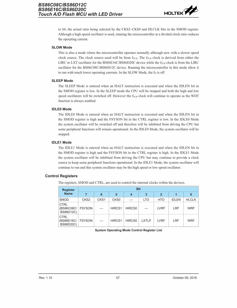
Rev. 1.10 56 October 09, 2018 Rev. 1.10 57 October 09, 2018
BS86C08C/BS86D12CBS86E16C/BS86D20C
Touch A/D Flash MCU with LED Driver
BS86C08C/BS86D12CBS86E16C/BS86D20CTouch A/D Flash MCU with LED Driver
to 64, the actual ratio being selected by the CKS2~CKS0 and HLCLK bits in the SMOD register. Although a high speed oscillator is used, running the microcontroller at a divided clock ratio reduces the operating current.
SLOW ModeThis is also a mode where the microcontroller operates normally although now with a slower speed clock source. The clock source used will be from fSUB. The fSUB clock is derived from either the LIRC or LXT oscillator for the BS86E16C/BS86D20C device while the fSUB clock is from the LIRC oscillator for the BS86C08C/BS86D12C device. Running the microcontroller in this mode allow it to run with much lower operating currents. In the SLOW Mode, the fH is off.
SLEEP ModeThe SLEEP Mode is entered when an HALT instruction is executed and when the IDLEN bit in the SMOD register is low. In the SLEEP mode the CPU will be stopped and both the high and low speed oscillators will be switched off. However the fSUB clock will continue to operate as the WDT function is always enabled.
IDLE0 ModeThe IDLE0 Mode is entered when an HALT instruction is executed and when the IDLEN bit in the SMOD register is high and the FSYSON bit in the CTRL register is low. In the IDLE0 Mode the system oscillator will be switched off and therefore will be inhibited from driving the CPU but some peripheral functions will remain operational. In the IDLE0 Mode, the system oscillator will be stopped.
IDLE1 ModeThe IDLE1 Mode is entered when an HALT instruction is executed and when the IDLEN bit in the SMOD register is high and the FSYSON bit in the CTRL register is high. In the IDLE1 Mode the system oscillator will be inhibited from driving the CPU but may continue to provide a clock source to keep some peripheral functions operational. In the IDLE1 Mode, the system oscillator will continue to run and this system oscillator may be the high speed or low speed oscillator.
Control RegistersThe registers, SMOD and CTRL, are used to control the internal clocks within the devices.
Register Name
Bit
7 6 5 4 3 2 1 0SMOD CKS2 CKS1 CKS0 — LTO HTO IDLEN HLCLKCTRL(BS86C08C/ BS86D12C)
FSYSON — HIRCS1 HIRCS0 — LVRF LRF WRF
CTRL(BS86E16C/ BS86D20C)
FSYSON — HIRCS1 HIRCS0 LXTLP LVRF LRF WRF
System Operating Mode Control Register List

Rev. 1.10 58 October 09, 2018 Rev. 1.10 59 October 09, 2018
BS86C08C/BS86D12CBS86E16C/BS86D20C
Touch A/D Flash MCU with LED Driver
BS86C08C/BS86D12CBS86E16C/BS86D20CTouch A/D Flash MCU with LED Driver
• SMOD Register
Bit 7 6 5 4 3 2 1 0Name CKS2 CKS1 CKS0 — LTO HTO IDLEN HLCLKR/W R/W R/W R/W — R R R/W R/WPOR 0 0 0 — 0 0 1 1
Bit 7~5 CKS2~CKS0: System clock selection when HLCLK is “0”000: fSUB (LIRC or LXT)001: fSUB (LIRC or LXT)010: fH/64011: fH/32100: fH/16101: fH/8110: fH/4111: fH/2
These three bits are used to select which clock is used as the system clock source. In addition to the system clock source, which can be either the LXT or LIRC, a divided version of the high speed system oscillator can also be chosen as the system clock source. Note that the LXT oscillator is only available for the BS86E16C/BS86D20C device.
Bit 4 Unimplemented, read as “0”Bit 3 LTO: Low speed system oscillator ready flag
0: Not ready1: Ready
This is the low speed system oscillator ready flag which indicates when the low speed system oscillator is stable after power on reset or a wake-up has occurred. The flag will be low when in the SLEEP Mode but after a wake-up has occurred, the flag will change to a high level after 128 clock cycles if LXT oscillator is used and 1~2 clock cycles if the LIRC oscillator is used.
Bit 2 HTO: High speed system oscillator ready flag0: Not ready1: Ready
This is the high speed system oscillator ready flag which indicates when the high speed system oscillator is stable after a wake-up has occurred. This flag is cleared to zero by hardware when the device is powered on and then changes to a high level after the high speed system oscillator is stable. Therefore, this flag will always be read as “1” by the application program after device power-on. The flag will be low when in the SLEEP or IDLE0 Mode but after power on reset or a wake-up has occurred, the flag will change to a high level after 15~16 clock cycles if the HIRC oscillator is used.
Bit 1 IDLEN: IDLE Mode Control0: Disable1: Enable
This bit is the IDLE Mode control bit and determines what happens when the HALT instruction is executed. If this bit is high, when a HALT instruction is executed the device will enter the IDLE Mode. In the IDLE1 Mode the CPU will stop running but the system clock will continue to keep the peripheral functions operational, if FSYSON bit is high. If the FSYSON bit is low, the CPU and the system clock will all stop in the IDLE0 Mode. If the bit is low the device will enter the SLEEP Mode when a HALT instruction is executed.
Bit 0 HLCLK: System clock selection0: fH/2~fH/64 or fSUB
1: fH
This bit is used to select if the fH clock, the fH/2~fH/64 or fSUB clock is used as the system clock. When this bit is high the fH clock will be selected and if low the fH/2~fH/64 or fSUB clock will be selected. When the system clock is switched from the fH clock to the fSUB clock, the fH clock will automatically be switched off to conserve power.

Rev. 1.10 58 October 09, 2018 Rev. 1.10 59 October 09, 2018
BS86C08C/BS86D12CBS86E16C/BS86D20C
Touch A/D Flash MCU with LED Driver
BS86C08C/BS86D12CBS86E16C/BS86D20CTouch A/D Flash MCU with LED Driver
• CTRL Register – BS86C08C/BS86D12C
Bit 7 6 5 4 3 2 1 0Name FSYSON — HIRCS1 HIRCS0 — LVRF LRF WRFR/W R/W — R/W R/W — R/W R/W R/WPOR 0 — 0 0 — x 0 0
“x”: unknown
• CTRL Register – BS86E16C/BS86D20C
Bit 7 6 5 4 3 2 1 0Name FSYSON — HIRCS1 HIRCS0 LXTLP LVRF LRF WRFR/W R/W — R/W R/W R/W R/W R/W R/WPOR 0 — 0 0 0 x 0 0
“x”: unknownBit 7 FSYSON: fSYS Control in IDLE Mode
0: Disable1: Enable
Bit 6 Unimplemented, read as “0”Bit 5~4 HIRCS1~HIRCS0: HIRC frequency selection
00: 8MHz01: 12MHz10: 16MHz11: 8MHz
It is recommended that the HIRC frequency selected by these two bits should be the same with the frequency determined by the configuration option to achieve the HIRC frequency accuracy specified in the A.C. characteristics.
Bit 3 LXTLP: LXT low power control0: Quick Start mode1: Low Power mode
Note that this bit is used to select the operating mode of the LXT oscillator which is only available for the BS86E16C/BS86D20C device. For the BS86C08C/BS86D12C device this bit is unimplemented and is read as “0”.
Bit 2 LVRF: LVR function reset flagDescribed elsewhere
Bit 1 LRF: LVR control register software reset flagDescribed elsewhere
Bit 0 WRF: WDT control register software reset flagDescribed elsewhere
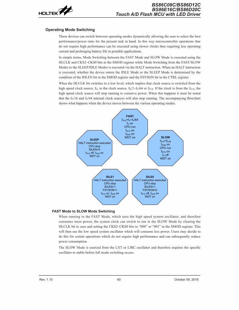
Rev. 1.10 60 October 09, 2018 Rev. 1.10 61 October 09, 2018
BS86C08C/BS86D12CBS86E16C/BS86D20C
Touch A/D Flash MCU with LED Driver
BS86C08C/BS86D12CBS86E16C/BS86D20CTouch A/D Flash MCU with LED Driver
Operating Mode SwitchingThese devices can switch between operating modes dynamically allowing the user to select the best performance/power ratio for the present task in hand. In this way microcontroller operations that do not require high performance can be executed using slower clocks thus requiring less operating current and prolonging battery life in portable applications.
In simple terms, Mode Switching between the FAST Mode and SLOW Mode is executed using the HLCLK and CKS2~CKS0 bits in the SMOD register while Mode Switching from the FAST/SLOW Modes to the SLEEP/IDLE Modes is executed via the HALT instruction. When an HALT instruction is executed, whether the device enters the IDLE Mode or the SLEEP Mode is determined by the condition of the IDLEN bit in the SMOD register and the FSYSON bit in the CTRL register.
When the HLCLK bit switches to a low level, which implies that clock source is switched from the high speed clock source, fH, to the clock source, fH/2~fH/64 or fSUB. If the clock is from the fSUB, the high speed clock source will stop running to conserve power. When this happens it must be noted that the fH/16 and fH/64 internal clock sources will also stop running. The accompanying flowchart shows what happens when the device moves between the various operating modes.
FASTfSYS=fH~fH/64
fH onCPU runfSYS onfSUB on
WDT on SLOWfSYS=fSUBfSUB on
CPU runfSYS onfH off
WDT on
IDLE0HALT instruction executed
CPU stopIDLEN=1
FSYSON=0fSYS off, fSUB on
WDT on
SLEEPHALT instruction executed
CPU stopIDLEN=0
fSYS off, fSUB onWDT on
IDLE1HALT instruction executed
CPU stopIDLEN=1
FSYSON=1fSYS on, fSUB on
WDT on
FAST Mode to SLOW Mode SwitchingWhen running in the FAST Mode, which uses the high speed system oscillator, and therefore consumes more power, the system clock can switch to run in the SLOW Mode by clearing the HLCLK bit to zero and setting the CKS2~CKS0 bits to “000” or “001” in the SMOD register. This will then use the low speed system oscillator which will consume less power. Users may decide to do this for certain operations which do not require high performance and can subsequently reduce power consumption.
The SLOW Mode is sourced from the LXT or LIRC oscillator and therefore requires the specific oscillator to stable before full mode switching occurs.

Rev. 1.10 60 October 09, 2018 Rev. 1.10 61 October 09, 2018
BS86C08C/BS86D12CBS86E16C/BS86D20C
Touch A/D Flash MCU with LED Driver
BS86C08C/BS86D12CBS86E16C/BS86D20CTouch A/D Flash MCU with LED Driver
FAST Mode
SLOW Mode
CKS2~CKS0=00xB & HLCLK=0
SLEEP Mode
IDLEN=0 & HALT instruction is executed
IDLE0 Mode
IDLEN=1, FSYSON=0HALT instruction is executed
IDLE1 Mode
IDLEN=1, FSYSON=1HALT instruction is executed
SLOW Mode to FAST Mode SwitchingIn SLOW mode the system uses the fSUB clock derived from either the LXT or LIRC low speed oscillator as system clock. When system clock is switched back to the FAST mode from fSUB, where the high speed system oscillator is used, the HLCLK bit should be set high or HLCLK bit is low but the CKS2~CKS0 bits are set to “010~111” and then the system clock will respectively be switched to fH~fH/64.
However, if fH is not used in SLOW mode and thus switched off, it will take some time to re-oscillate and stabilise when switching back to the FAST mode from the SLOW Mode and the status of the HTO flag should be checked. The time duration required for the high speed system oscillator stabilization is specified in the relevant characteristics.
SLOW Mode
FAST Mode
CKS2~CKS0≠00xB & as HLCLK=0 or HLCLK=1
SLEEP Mode
IDLEN=0 & HALT instruction is executed
IDLE0 Mode
IDLEN=1, FSYSON=0HALT instruction is executed
IDLE1 Mode
IDLEN=1, FSYSON=1HALT instruction is executed
Entering the SLEEP ModeThere is only one way for the device to enter the SLEEP Mode and that is to execute the “HALT” instruction in the application program with the IDLEN bit in the SMOD register equal to “0”. In this mode all the clocks and functions will be switched off except the WDT function. When this instruction is executed under the conditions described above, the following will occur:

Rev. 1.10 62 October 09, 2018 Rev. 1.10 63 October 09, 2018
BS86C08C/BS86D12CBS86E16C/BS86D20C
Touch A/D Flash MCU with LED Driver
BS86C08C/BS86D12CBS86E16C/BS86D20CTouch A/D Flash MCU with LED Driver
• The system clock will be stopped and the application program will stop at the “HALT” instruction.
• The Data Memory contents and registers will maintain their present condition.
• The I/O ports will maintain their present conditions.
• In the status register, the Power Down flag PDF will be set, and WDT timeout flag TO will be cleared.
• The WDT will be cleared and resume counting as the WDT function is always enabled.
Entering the IDLE0 ModeThere is only one way for the device to enter the IDLE0 Mode and that is to execute the “HALT” instruction in the application program with the IDLEN bit in the SMOD register equal to “1” and the FSYSON bit in the CTRL register equal to “0”. When this instruction is executed under the conditions described above, the following will occur:
• The system clock will be stopped and the application program will stop at the “HALT” instruction, but the low frequency clock fSUB will be on.
• The Data Memory contents and registers will maintain their present condition.
• The I/O ports will maintain their present conditions.
• In the status register, the Power Down flag PDF will be set, and WDT timeout flag TO will be cleared.
• The WDT will be cleared and resume counting.
Entering the IDLE1 ModeThere is only one way for the device to enter the IDLE1 Mode and that is to execute the “HALT” instruction in the application program with the IDLEN bit in the SMOD register is equal to “1” and the FSYSON bit in the CTRL register equal to “1”. When this instruction is executed under the conditions described above, the following will occur:
• The system and the low frequency fSUB clocks will be on but the application program will stop at the “HALT” instruction.
• The Data Memory contents and registers will maintain their present condition.
• The I/O ports will maintain their present conditions.
• In the status register, the Power Down flag PDF will be set, and WDT timeout flag TO will be cleared.
• The WDT will be cleared and resume counting.
Standby Current ConsiderationsAs the main reason for entering the SLEEP or IDLE Mode is to keep the current consumption of the device to as low a value as possible, perhaps only in the order of several micro-amps except in the IDLE1 Mode, there are other considerations which must also be taken into account by the circuit designer if the power consumption is to be minimised. Special attention must be made to the I/O pins on the device. All high-impedance input pins must be connected to either a fixed high or low level as any floating input pins could create internal oscillations and result in increased current consumption. This also applies to devices which have different package types, as there may be unbonded pins. These must either be setup as outputs or if setup as inputs must have pull-high resistors connected.
Care must also be taken with the loads, which are connected to I/O pins, which are setup as outputs. These should be placed in a condition in which minimum current is drawn or connected only to external circuits that do not draw current, such as other CMOS inputs. Also note that additional standby current will also be consumed if the LIRC or LXT oscillator has enabled.
In the IDLE1 Mode the system oscillator is on, if the peripheral function clock source is derived from the high speed oscillator, the additional standby current will also be perhaps in the order of several hundred micro-amps.
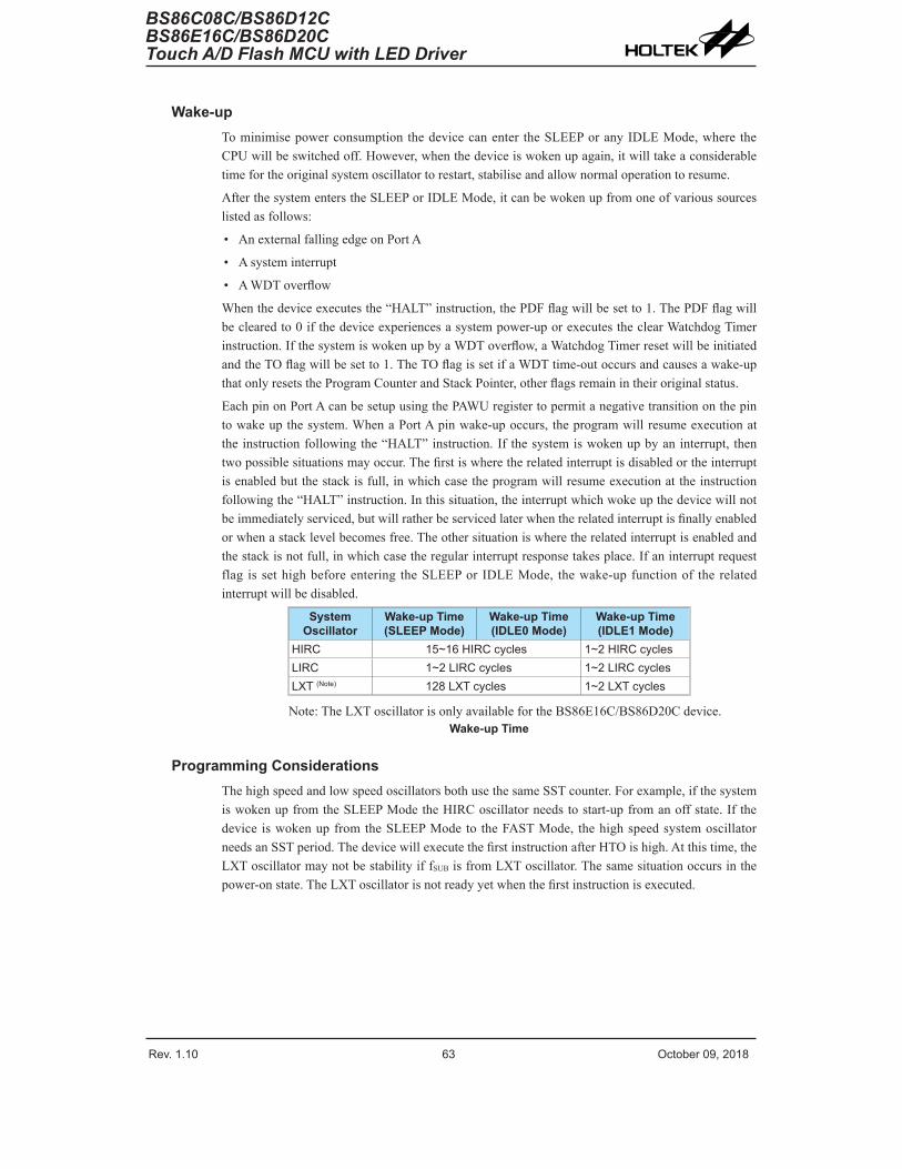
Rev. 1.10 62 October 09, 2018 Rev. 1.10 63 October 09, 2018
BS86C08C/BS86D12CBS86E16C/BS86D20C
Touch A/D Flash MCU with LED Driver
BS86C08C/BS86D12CBS86E16C/BS86D20CTouch A/D Flash MCU with LED Driver
Wake-upTo minimise power consumption the device can enter the SLEEP or any IDLE Mode, where the CPU will be switched off. However, when the device is woken up again, it will take a considerable time for the original system oscillator to restart, stabilise and allow normal operation to resume.
After the system enters the SLEEP or IDLE Mode, it can be woken up from one of various sources listed as follows:
• An external falling edge on Port A
• A system interrupt
• A WDT overflow
When the device executes the “HALT” instruction, the PDF flag will be set to 1. The PDF flag will be cleared to 0 if the device experiences a system power-up or executes the clear Watchdog Timer instruction. If the system is woken up by a WDT overflow, a Watchdog Timer reset will be initiated and the TO flag will be set to 1. The TO flag is set if a WDT time-out occurs and causes a wake-up that only resets the Program Counter and Stack Pointer, other flags remain in their original status.
Each pin on Port A can be setup using the PAWU register to permit a negative transition on the pin to wake up the system. When a Port A pin wake-up occurs, the program will resume execution at the instruction following the “HALT” instruction. If the system is woken up by an interrupt, then two possible situations may occur. The first is where the related interrupt is disabled or the interrupt is enabled but the stack is full, in which case the program will resume execution at the instruction following the “HALT” instruction. In this situation, the interrupt which woke up the device will not be immediately serviced, but will rather be serviced later when the related interrupt is finally enabled or when a stack level becomes free. The other situation is where the related interrupt is enabled and the stack is not full, in which case the regular interrupt response takes place. If an interrupt request flag is set high before entering the SLEEP or IDLE Mode, the wake-up function of the related interrupt will be disabled.
System Oscillator
Wake-up Time(SLEEP Mode)
Wake-up Time(IDLE0 Mode)
Wake-up Time(IDLE1 Mode)
HIRC 15~16 HIRC cycles 1~2 HIRC cyclesLIRC 1~2 LIRC cycles 1~2 LIRC cyclesLXT (Note) 128 LXT cycles 1~2 LXT cycles
Note: The LXT oscillator is only available for the BS86E16C/BS86D20C device.Wake-up Time
Programming ConsiderationsThe high speed and low speed oscillators both use the same SST counter. For example, if the system is woken up from the SLEEP Mode the HIRC oscillator needs to start-up from an off state. If the device is woken up from the SLEEP Mode to the FAST Mode, the high speed system oscillator needs an SST period. The device will execute the first instruction after HTO is high. At this time, the LXT oscillator may not be stability if fSUB is from LXT oscillator. The same situation occurs in the power-on state. The LXT oscillator is not ready yet when the first instruction is executed.

Rev. 1.10 64 October 09, 2018 Rev. 1.10 65 October 09, 2018
BS86C08C/BS86D12CBS86E16C/BS86D20C
Touch A/D Flash MCU with LED Driver
BS86C08C/BS86D12CBS86E16C/BS86D20CTouch A/D Flash MCU with LED Driver
Watchdog TimerThe Watchdog Timer is provided to prevent program malfunctions or sequences from jumping to unknown locations, due to certain uncontrollable external events such as electrical noise.
Watchdog Timer Clock SourceThe Watchdog Timer clock source is provided by the internal fSUB clock which is in turn supplied by either the LXT or LIRC oscillator selected by a configuration option. The LIRC internal oscillator has an approximate frequency of 32kHz and this specified internal clock period can vary with VDD, temperature and process variations. The LXT oscillator is supplied by an external 32.768kHz crystal. The Watchdog Timer source clock is then subdivided by a ratio of 28 to 218 to give longer timeouts, the actual value being chosen using the WS2~WS0 bits in the WDTC register.
Watchdog Timer Control RegisterA single register, WDTC, controls the required timeout period as well as the enable/reset control. This register controls the overall operation of the Watchdog Timer. The WDTC register is initiated to 01010011B at any reset except the WDT time-out hardware warm reset.
• WDTC Register
Bit 7 6 5 4 3 2 1 0Name WE4 WE3 WE2 WE1 WE0 WS2 WS1 WS0R/W R/W R/W R/W R/W R/W R/W R/W R/WPOR 0 1 0 1 0 0 1 1
Bit 7~3 WE4~WE0: WDT function control01010 or 10101: EnableOther values: Reset MCU
If these bits are changed due to adverse environmental conditions, the microcontroller will be reset. The reset operation will be activated after a delay time, tSRESET, and the WRF bit in the CTRL register will be set high.
Bit 2~0 WS2~WS0: WDT time-out period selection000: 28/fSUB
001: 210/fSUB
010: 212/fSUB
011: 214/fSUB
100: 215/fSUB
101: 216/fSUB
110: 217/fSUB
111: 218/fSUB
These three bits determine the division ratio of the watchdog timer source clock, which in turn determines the time-out period.
• CTRL Register – BS86C08C/BS86D12C
Bit 7 6 5 4 3 2 1 0Name FSYSON — HIRCS1 HIRCS0 — LVRF LRF WRFR/W R/W — R/W R/W — R/W R/W R/WPOR 0 — 0 0 — x 0 0
“x”: unknown

Rev. 1.10 64 October 09, 2018 Rev. 1.10 65 October 09, 2018
BS86C08C/BS86D12CBS86E16C/BS86D20C
Touch A/D Flash MCU with LED Driver
BS86C08C/BS86D12CBS86E16C/BS86D20CTouch A/D Flash MCU with LED Driver
• CTRL Register – BS86E16C/BS86D20C
Bit 7 6 5 4 3 2 1 0Name FSYSON — HIRCS1 HIRCS0 LXTLP LVRF LRF WRFR/W R/W — R/W R/W R/W R/W R/W R/WPOR 0 — 0 0 0 x 0 0
“x”: unknownBit 7 FSYSON: fSYS Control in IDLE Mode
Described elsewhereBit 6 Unimplemented, read as “0”Bit 5~4 HIRCS1~HIRCS0: HIRC frequency selection
Described elsewhereBit 3 LXTLP: LXT low power control
Described elsewhereBit 2 LVRF: LVR function reset flag
Described elsewhereBit 1 LRF: LVR control register software reset flag
Described elsewhereBit 0 WRF: WDT control register software reset flag
0: Not occur1: Occurred
This bit is set high by the WDT control register software reset and cleared by the application program. Note that this bit can only be cleared to zero by the application program.
Watchdog Timer OperationThe Watchdog Timer operates by providing a device reset when its timer overflows. This means that in the application program and during normal operation the user has to strategically clear the Watchdog Timer before it overflows to prevent the Watchdog Timer from executing a reset. This is done using the clear watchdog instruction. If the program malfunctions for whatever reason, jumps to an unknown location, or enters an endless loop, the clear instruction will not be executed in the correct manner, in which case the Watchdog Timer will overflow and reset the device. With regard to the Watchdog Timer function control, there are five bits, WE4~WE0, in the WDTC register to offer the enable and reset control of the Watchdog Timer. The WDT function will be enabled when the WE4~WE0 bits are set to a value of 01010B or 10101B. If the WE4~WE0 bits are changed to any other values rather than 01010B and 10101B, which is caused by the environmental noise, it will reset the device after a delay time, tSRESET. After power on these bits will have a value of 01010B.
WE4~WE0 Bits WDT Function01010B or 10101B Enable
Any other value Reset MCU
Watchdog Timer Enable/Reset Control
Under normal program operation, a Watchdog Timer time-out will initialise a device reset and set the status bit TO. However, if the system is in the SLEEP or IDLE Mode, when a Watchdog Timer time-out occurs, the TO bit in the status register will be set and only the Program Counter and Stack Pointer will be reset. Three methods can be adopted to clear the contents of the Watchdog Timer. The first is a WDTC software reset, which means a certain value except 01010B and 10101B written into the WE4~WE0 field, the second is using the Watchdog Timer software clear instruction and the third is via a HALT instruction.

Rev. 1.10 66 October 09, 2018 Rev. 1.10 67 October 09, 2018
BS86C08C/BS86D12CBS86E16C/BS86D20C
Touch A/D Flash MCU with LED Driver
BS86C08C/BS86D12CBS86E16C/BS86D20CTouch A/D Flash MCU with LED Driver
There is only one method of using software instruction to clear the Watchdog Timer. That is to use the single “CLR WDT” instruction to clear the WDT contents.
The maximum time out period is when the 218 division ratio is selected. As an example, with a 32kHz LIRC oscillator as its source clock, this will give a maximum watchdog period of around 8 second for the 218 division ratio and a minimum timeout of 8ms for the 28 division ration.
8-stage Divider WDT Prescaler
WE4~WE0 bitsWDTC Register Reset MCU
fSUB/28
8-to-1 MUX
CLR
WS2~WS0 WDT Time-out(28/fSUB~218/fSUB)
fSUB
ConfigurationOption
LXT *
LIRC
“CLR WDT”Instruction“HALT”Instruction
Note: The LXT oscillator is only available for the BS86E16C/BS86D20C device.Watchdog Timer
Reset and InitialisationA reset function is a fundamental part of any microcontroller ensuring that the device can be set to some predetermined condition irrespective of outside parameters. The most important reset condition is after power is first applied to the microcontroller. In this case, internal circuitry will ensure that the microcontroller, after a short delay, will be in a well-defined state and ready to execute the first program instruction. After this power-on reset, certain important internal registers will be set to defined states before the program commences. One of these registers is the Program Counter, which will be reset to zero forcing the microcontroller to begin program execution from the lowest Program Memory address.
In addition to the power-on reset, another reset exists in the form of a Low Voltage Reset, LVR, where a full reset is implemented in situations where the power supply voltage falls below a certain threshold. Another type of reset is when the Watchdog Timer overflows and resets the microcontroller. All types of reset operations result in different register conditions being setup.
Reset FunctionsThere are several ways in which a microcontroller reset can occur, through events occurring internally.
Power-on ResetThe most fundamental and unavoidable reset is the one that occurs after power is first applied to the microcontroller. As well as ensuring that the Program Memory begins execution from the first memory address, a power-on reset also ensures that certain other registers are preset to known conditions. All the I/O port and port control registers will power up in a high condition ensuring that all pins will be first set to inputs.
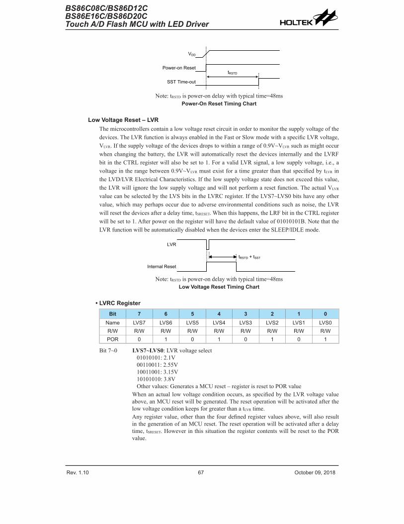
Rev. 1.10 66 October 09, 2018 Rev. 1.10 67 October 09, 2018
BS86C08C/BS86D12CBS86E16C/BS86D20C
Touch A/D Flash MCU with LED Driver
BS86C08C/BS86D12CBS86E16C/BS86D20CTouch A/D Flash MCU with LED Driver
VDD
Power-on Reset
SST Time-out
tRSTD
Note: tRSTD is power-on delay with typical time=48msPower-On Reset Timing Chart
Low Voltage Reset – LVRThe microcontrollers contain a low voltage reset circuit in order to monitor the supply voltage of the devices. The LVR function is always enabled in the Fast or Slow mode with a specific LVR voltage, VLVR. If the supply voltage of the devices drops to within a range of 0.9V~VLVR such as might occur when changing the battery, the LVR will automatically reset the devices internally and the LVRF bit in the CTRL register will also be set to 1. For a valid LVR signal, a low supply voltage, i.e., a voltage in the range between 0.9V~VLVR must exist for a time greater than that specified by tLVR in the LVD/LVR Electrical Characteristics. If the low supply voltage state does not exceed this value, the LVR will ignore the low supply voltage and will not perform a reset function. The actual VLVR value can be selected by the LVS bits in the LVRC register. If the LVS7~LVS0 bits have any other value, which may perhaps occur due to adverse environmental conditions such as noise, the LVR will reset the devices after a delay time, tSRESET. When this happens, the LRF bit in the CTRL register will be set to 1. After power on the register will have the default value of 01010101B. Note that the LVR function will be automatically disabled when the devices enter the SLEEP/IDLE mode.
LVR
Internal Reset
tRSTD + tSST
Note: tRSTD is power-on delay with typical time=48msLow Voltage Reset Timing Chart
• LVRC Register
Bit 7 6 5 4 3 2 1 0Name LVS7 LVS6 LVS5 LVS4 LVS3 LVS2 LVS1 LVS0R/W R/W R/W R/W R/W R/W R/W R/W R/WPOR 0 1 0 1 0 1 0 1
Bit 7~0 LVS7~LVS0: LVR voltage select01010101: 2.1V00110011: 2.55V10011001: 3.15V10101010: 3.8VOther values: Generates a MCU reset – register is reset to POR value
When an actual low voltage condition occurs, as specified by the LVR voltage value above, an MCU reset will be generated. The reset operation will be activated after the low voltage condition keeps for greater than a tLVR time.Any register value, other than the four defined register values above, will also result in the generation of an MCU reset. The reset operation will be activated after a delay time, tSRESET. However in this situation the register contents will be reset to the POR value.

Rev. 1.10 68 October 09, 2018 Rev. 1.10 69 October 09, 2018
BS86C08C/BS86D12CBS86E16C/BS86D20C
Touch A/D Flash MCU with LED Driver
BS86C08C/BS86D12CBS86E16C/BS86D20CTouch A/D Flash MCU with LED Driver
• CTRL Register – BS86C08C/BS86D12C
Bit 7 6 5 4 3 2 1 0Name FSYSON — HIRCS1 HIRCS0 — LVRF LRF WRFR/W R/W — R/W R/W — R/W R/W R/WPOR 0 — 0 0 — x 0 0
“x”: unknown
• CTRL Register – BS86E16C/BS86D20C
Bit 7 6 5 4 3 2 1 0Name FSYSON — HIRCS1 HIRCS0 LXTLP LVRF LRF WRFR/W R/W — R/W R/W R/W R/W R/W R/WPOR 0 — 0 0 0 x 0 0
“x”: unknownBit 7 FSYSON: fSYS Control in IDLE Mode
Described elsewhereBit 6 Unimplemented, read as “0”Bit 5~4 HIRCS1~HIRCS0: HIRC frequency selection
Described elsewhereBit 3 LXTLP: LXT low power control
Described elsewhereBit 2 LVRF: LVR function reset flag
0: Not occurred1: Occurred
This bit is set to 1 when a specific low voltage reset condition occurs. Note that this bit can only be cleared to 0 by the application program.
Bit 1 LRF: LVR control register software reset flag0: Not occurred1: Occurred
This bit is set to 1 by the LVRC control register contains any undefined LVR voltage register values. This in effect acts like a software-reset function. Note that this bit can only be cleared to 0 by the application program.
Bit 0 WRF: WDT control register software reset flagDescribed elsewhere
Watchdog Time-out Reset during Normal OperationThe Watchdog time-out Reset during normal operations in the FAST or SLOW mode is the same as the hardware Low Voltage Reset except that the Watchdog time-out flag TO will be set to “1”.
WDT Time-out
Internal Reset
tRSTD + tSST
Note: tRSTD is power-on delay with typical time=16msWDT Time-out Reset during Normal Operation Timing Chart
Watchdog Time-out Reset during SLEEP or IDLE ModeThe Watchdog time-out Reset during SLEEP or IDLE Mode is a little different from other kinds of reset. Most of the conditions remain unchanged except that the Program Counter and the Stack Pointer will be cleared to “0” and the TO flag will be set to “1”. Refer to the System Start Up Time Characteristics for tSST details.
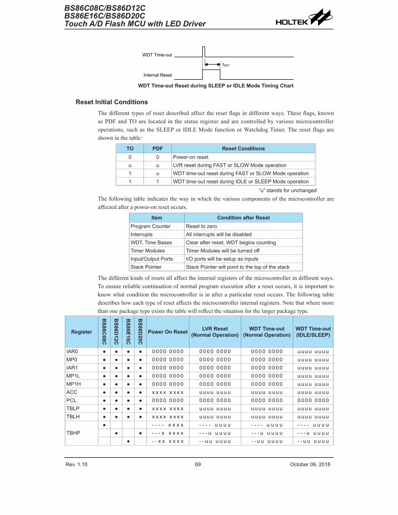
Rev. 1.10 68 October 09, 2018 Rev. 1.10 69 October 09, 2018
BS86C08C/BS86D12CBS86E16C/BS86D20C
Touch A/D Flash MCU with LED Driver
BS86C08C/BS86D12CBS86E16C/BS86D20CTouch A/D Flash MCU with LED Driver
WDT Time-out
Internal Reset
tSST
WDT Time-out Reset during SLEEP or IDLE Mode Timing Chart
Reset Initial ConditionsThe different types of reset described affect the reset flags in different ways. These flags, known as PDF and TO are located in the status register and are controlled by various microcontroller operations, such as the SLEEP or IDLE Mode function or Watchdog Timer. The reset flags are shown in the table:
TO PDF Reset Conditions0 0 Power-on resetu u LVR reset during FAST or SLOW Mode operation1 u WDT time-out reset during FAST or SLOW Mode operation1 1 WDT time-out reset during IDLE or SLEEP Mode operation
“u” stands for unchangedThe following table indicates the way in which the various components of the microcontroller are affected after a power-on reset occurs.
Item Condition after ResetProgram Counter Reset to zeroInterrupts All interrupts will be disabledWDT, Time Bases Clear after reset, WDT begins countingTimer Modules Timer Modules will be turned offInput/Output Ports I/O ports will be setup as inputsStack Pointer Stack Pointer will point to the top of the stack
The different kinds of resets all affect the internal registers of the microcontroller in different ways. To ensure reliable continuation of normal program execution after a reset occurs, it is important to know what condition the microcontroller is in after a particular reset occurs. The following table describes how each type of reset affects the microcontroller internal registers. Note that where more than one package type exists the table will reflect the situation for the larger package type.
Register
BS86C
08C
BS86D
12C
BS86E16C
BS86D
20C
Power On Reset LVR Reset(Normal Operation)
WDT Time-out (Normal Operation)
WDT Time-out (IDLE/SLEEP)
IAR0 ● ● ● ● 0 0 0 0 0 0 0 0 0 0 0 0 0 0 0 0 0 0 0 0 0 0 0 0 u u u u u u u uMP0 ● ● ● ● 0 0 0 0 0 0 0 0 0 0 0 0 0 0 0 0 0 0 0 0 0 0 0 0 u u u u u u u uIAR1 ● ● ● ● 0 0 0 0 0 0 0 0 0 0 0 0 0 0 0 0 0 0 0 0 0 0 0 0 u u u u u u u uMP1L ● ● ● ● 0 0 0 0 0 0 0 0 0 0 0 0 0 0 0 0 0 0 0 0 0 0 0 0 u u u u u u u uMP1H ● ● ● ● 0 0 0 0 0 0 0 0 0 0 0 0 0 0 0 0 0 0 0 0 0 0 0 0 u u u u u u u uACC ● ● ● ● x x x x x x x x u u u u u u u u u u u u u u u u u u u u u u u uPCL ● ● ● ● 0 0 0 0 0 0 0 0 0 0 0 0 0 0 0 0 0 0 0 0 0 0 0 0 0 0 0 0 0 0 0 0TBLP ● ● ● ● x x x x x x x x u u u u u u u u u u u u u u u u u u u u u u u uTBLH ● ● ● ● x x x x x x x x u u u u u u u u u u u u u u u u u u u u u u u u
TBHP● - - - - x x x x - - - - u u u u - - - - u u u u - - - - u u u u
● ● - - - x x x x x - - - u u u u u - - - u u u u u - - - u u u u u● - - x x x x x x - - u u u u u u - - u u u u u u - - u u u u u u
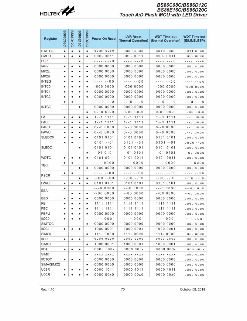
Rev. 1.10 70 October 09, 2018 Rev. 1.10 71 October 09, 2018
BS86C08C/BS86D12CBS86E16C/BS86D20C
Touch A/D Flash MCU with LED Driver
BS86C08C/BS86D12CBS86E16C/BS86D20CTouch A/D Flash MCU with LED Driver
Register
BS86C
08C
BS86D
12C
BS86E16C
BS86D
20C
Power On Reset LVR Reset(Normal Operation)
WDT Time-out (Normal Operation)
WDT Time-out (IDLE/SLEEP)
STATUS ● ● ● ● x x 0 0 x x x x u u u u u u u u u u 1 u u u u u u u 11 u u u uSMOD ● ● ● ● 0 0 0 - 0 0 11 0 0 0 - 0 0 11 0 0 0 - 0 0 11 u u u - u u u uPBP ● - - - - - - - 0 - - - - - - - 0 - - - - - - - 0 - - - - - - - uIAR2 ● ● ● ● 0 0 0 0 0 0 0 0 0 0 0 0 0 0 0 0 0 0 0 0 0 0 0 0 u u u u u u u uMP2L ● ● ● ● 0 0 0 0 0 0 0 0 0 0 0 0 0 0 0 0 0 0 0 0 0 0 0 0 u u u u u u u uMP2H ● ● ● ● 0 0 0 0 0 0 0 0 0 0 0 0 0 0 0 0 0 0 0 0 0 0 0 0 u u u u u u u uINTEG ● ● ● ● - - - - - - 0 0 - - - - - - 0 0 - - - - - - 0 0 - - - - - - u uINTC0 ● ● ● ● - 0 0 0 0 0 0 0 - 0 0 0 0 0 0 0 - 0 0 0 0 0 0 0 - u u u u u u uINTC1 ● ● ● ● 0 0 0 0 0 0 0 0 0 0 0 0 0 0 0 0 0 0 0 0 0 0 0 0 u u u u u u u uINTC2 ● ● ● ● 0 0 0 0 0 0 0 0 0 0 0 0 0 0 0 0 0 0 0 0 0 0 0 0 u u u u u u u u
INTC3● ● - - - 0 - - 0 - - - 0 - - - 0 - - - 0 - - - 0 - - - u - - - u
● 0 0 0 0 0 0 0 0 0 0 0 0 0 0 0 0 0 0 0 0 0 0 0 0 u u u u u u u u● 0 - 0 0 0 0 - 0 0 - 0 0 0 0 - 0 0 - 0 0 0 0 - 0 u - u u u u - u
PA ● ● ● ● 1 - - 1 1 1 1 1 1 - - 1 1 1 1 1 1 - - 1 1 1 1 1 u - - u u u u uPAC ● ● ● ● 1 - - 1 1 1 1 1 1 - - 1 1 1 1 1 1 - - 1 1 1 1 1 u - - u u u u uPAPU ● ● ● ● 0 - - 0 0 0 0 0 0 - - 0 0 0 0 0 0 - - 0 0 0 0 0 u - - u u u u uPAWU ● ● ● ● 0 - - 0 0 0 0 0 0 - - 0 0 0 0 0 0 - - 0 0 0 0 0 u - - u u u u uSLEDC0 ● ● ● ● 0 1 0 1 0 1 0 1 0 1 0 1 0 1 0 1 0 1 0 1 0 1 0 1 u u u u u u u u
SLEDC1● ● 0 1 0 1 - - 0 1 0 1 0 1 - - 0 1 0 1 0 1 - - 0 1 u u u u - - u u
● 0 1 0 1 0 1 0 1 0 1 0 1 0 1 0 1 0 1 0 1 0 1 0 1 u u u u u u u u● - - 0 1 0 1 0 1 - - 0 1 0 1 0 1 - - 0 1 0 1 0 1 - - u u u u u u
WDTC ● ● ● ● 0 1 0 1 0 0 11 0 1 0 1 0 0 11 0 1 0 1 0 0 11 u u u u u u u u
TBC● ● - - - - 0 0 0 0 - - - - 0 0 0 0 - - - - 0 0 0 0 - - - - u u u u
● ● 0 0 0 0 0 0 0 0 0 0 0 0 0 0 0 0 0 0 0 0 0 0 0 0 u u u u u u u u
PSCR● ● - - - - - - 0 0 - - - - - - 0 0 - - - - - - 0 0 - - - - - - u u
● ● - - 0 0 - - 0 0 - - 0 0 - - 0 0 - - 0 0 - - 0 0 - - u u - - u uLVRC ● ● ● ● 0 1 0 1 0 1 0 1 0 1 0 1 0 1 0 1 0 1 0 1 0 1 0 1 u u u u u u u u
EEA● - - - 0 0 0 0 0 - - - 0 0 0 0 0 - - - 0 0 0 0 0 - - - u u u u u
● ● ● - - 0 0 0 0 0 0 - - 0 0 0 0 0 0 - - 0 0 0 0 0 0 - - u u u u u uEED ● ● ● ● 0 0 0 0 0 0 0 0 0 0 0 0 0 0 0 0 0 0 0 0 0 0 0 0 u u u u u u u uPB ● ● ● ● 1 1 1 1 1 1 1 1 1 1 1 1 1 1 1 1 1 1 1 1 1 1 1 1 u u u u u u u uPBC ● ● ● ● 1 1 1 1 1 1 1 1 1 1 1 1 1 1 1 1 1 1 1 1 1 1 1 1 u u u u u u u uPBPU ● ● ● ● 0 0 0 0 0 0 0 0 0 0 0 0 0 0 0 0 0 0 0 0 0 0 0 0 u u u u u u u uIICC0 ● ● ● - - - - 0 0 0 - - - - - 0 0 0 - - - - - 0 0 0 - - - - - u u u -SIMTOC ● 0 0 0 0 0 0 0 0 0 0 0 0 0 0 0 0 0 0 0 0 0 0 0 0 u u u u u u u uIICC1 ● ● ● 1 0 0 0 0 0 0 1 1 0 0 0 0 0 0 1 1 0 0 0 0 0 0 1 u u u u u u u uSIMC0 ● 111 - 0 0 0 0 111 - 0 0 0 0 111 - 0 0 0 0 u u u - u u u uIICD ● ● ● x x x x x x x x x x x x x x x x x x x x x x x x u u u u u u u uSIMC1 ● 1 0 0 0 0 0 0 1 1 0 0 0 0 0 0 1 1 0 0 0 0 0 0 1 u u u u u u u uIICA ● ● ● 0 0 0 0 0 0 0 - 0 0 0 0 0 0 0 - 0 0 0 0 0 0 0 - u u u u u u u -SIMD ● x x x x x x x x x x x x x x x x x x x x x x x x u u u u u u u uIICTOC ● ● ● 0 0 0 0 0 0 0 0 0 0 0 0 0 0 0 0 0 0 0 0 0 0 0 0 u u u u u u u uSIMA/SIMC2 ● 0 0 0 0 0 0 0 0 0 0 0 0 0 0 0 0 0 0 0 0 0 0 0 0 u u u u u u u uU0SR ● ● ● ● 0 0 0 0 1 0 11 0 0 0 0 1 0 11 0 0 0 0 1 0 11 u u u u u u u uU0CR1 ● ● ● ● 0 0 0 0 0 0 x 0 0 0 0 0 0 0 x 0 0 0 0 0 0 0 x 0 u u u u u u u u

Rev. 1.10 70 October 09, 2018 Rev. 1.10 71 October 09, 2018
BS86C08C/BS86D12CBS86E16C/BS86D20C
Touch A/D Flash MCU with LED Driver
BS86C08C/BS86D12CBS86E16C/BS86D20CTouch A/D Flash MCU with LED Driver
Register
BS86C
08C
BS86D
12C
BS86E16C
BS86D
20C
Power On Reset LVR Reset(Normal Operation)
WDT Time-out (Normal Operation)
WDT Time-out (IDLE/SLEEP)
U0CR2 ● ● ● ● 0 0 0 0 0 0 0 0 0 0 0 0 0 0 0 0 0 0 0 0 0 0 0 0 u u u u u u u uTXR_RXR0 ● ● ● ● x x x x x x x x x x x x x x x x x x x x x x x x u u u u u u u uBRG0 ● ● ● ● x x x x x x x x x x x x x x x x x x x x x x x x u u u u u u u u
SADOL ● ● ● ● x x x x - - - - x x x x - - - - x x x x - - - -
u u u u - - - -(ADRFS=0)u u u u u u u u(ADRFS=1)
SADOH ● ● ● ● x x x x x x x x x x x x x x x x x x x x x x x x
u u u u u u u u(ADRFS=0)- - - - u u u u(ADRFS=1)
SADC0 ● ● ● ● 0 0 0 0 0 0 0 0 0 0 0 0 0 0 0 0 0 0 0 0 0 0 0 0 u u u u u u u uSADC1 ● ● ● ● 0 0 0 0 0 0 0 0 0 0 0 0 0 0 0 0 0 0 0 0 0 0 0 0 u u u u u u u uACERL ● ● ● ● 0 0 0 0 0 0 0 0 0 0 0 0 0 0 0 0 0 0 0 0 0 0 0 0 u u u u u u u u
TMPC● ● 0 - - - 0 0 0 0 0 - - - 0 0 0 0 0 - - - 0 0 0 0 u - - - u u u u
● ● 0 - 0 0 0 0 0 0 0 - 0 0 0 0 0 0 0 - 0 0 0 0 0 0 u - u u u u u uIFS0 ● ● ● ● 0 0 0 0 0 0 0 0 0 0 0 0 0 0 0 0 0 0 0 0 0 0 0 0 u u u u u u u u
IFS1● ● - - - - 0 - 0 - - - - 0 - 0 - - - - 0 - 0 - - - - - u - u
● 0 0 0 0 0 0 0 0 0 0 0 0 0 0 0 0 0 0 0 0 0 0 0 0 u u u u u u u u● - - - - - 1 1 1 - - - - - 1 1 1 - - - - - 1 1 1 - - - - - u u u
IFS2● ● - 0 - - - - - - - 0 - - - - - - - 0 - - - - - - - 0 - - - - - -
● 0 0 0 0 0 0 0 0 0 0 0 0 0 0 0 0 0 0 0 0 0 0 0 0 u u u u u u u uLVDC ● ● ● ● - - 0 0 0 0 0 0 - - 0 0 0 0 0 0 - - 0 0 0 0 0 0 - - u u u u u u
PC● ● - - - - 1 1 1 1 - - - - 1 1 1 1 - - - - 1 1 1 1 - - - - u u u u
● ● 1 1 1 1 1 1 1 1 1 1 1 1 1 1 1 1 1 1 1 1 1 1 1 1 u u u u u u u u
PCC● ● - - - - 1 1 1 1 - - - - 1 1 1 1 - - - - 1 1 1 1 - - - - u u u u
● ● 1 1 1 1 1 1 1 1 1 1 1 1 1 1 1 1 1 1 1 1 1 1 1 1 u u u u u u u u
PCPU● ● - - - - 0 0 0 0 - - - - 0 0 0 0 - - - - 0 0 0 0 - - - - u u u u
● ● 0 0 0 0 0 0 0 0 0 0 0 0 0 0 0 0 0 0 0 0 0 0 0 0 u u u u u u u uMFI ● ● - - 0 0 - - 0 0 - - 0 0 - - 0 0 - - 0 0 - - 0 0 - - u u - - u u
CTRL● ● 0 - 0 0 - x 0 0 0 - 0 0 - 1 0 0 0 - 0 0 - x 0 0 u - u u - u u u
● ● 0 - 0 0 0 x 0 0 0 - 0 0 0 1 0 0 0 - 0 0 0 x 0 0 u - u u u u u u
PD● ● ● 1 1 1 1 1 1 1 1 1 1 1 1 1 1 1 1 1 1 1 1 1 1 1 1 u u u u u u u u
● - - - - 1 1 1 1 - - - - 1 1 1 1 - - - - 1 1 1 1 - - - - u u u u
PDC● ● ● 1 1 1 1 1 1 1 1 1 1 1 1 1 1 1 1 1 1 1 1 1 1 1 1 u u u u u u u u
● - - - - 1 1 1 1 - - - - 1 1 1 1 - - - - 1 1 1 1 - - - - u u u u
PDPU● ● ● 0 0 0 0 0 0 0 0 0 0 0 0 0 0 0 0 0 0 0 0 0 0 0 0 u u u u u u u u
● - - - - 0 0 0 0 - - - - 0 0 0 0 - - - - 0 0 0 0 - - - - u u u uPE ● 1 1 1 1 1 1 1 1 1 1 1 1 1 1 1 1 1 1 1 1 1 1 1 1 u u u u u u u uPEC ● 1 1 1 1 1 1 1 1 1 1 1 1 1 1 1 1 1 1 1 1 1 1 1 1 u u u u u u u uPEPU ● 0 0 0 0 0 0 0 0 0 0 0 0 0 0 0 0 0 0 0 0 0 0 0 0 u u u u u u u uTKTMR ● ● ● ● 0 0 0 0 0 0 0 0 0 0 0 0 0 0 0 0 0 0 0 0 0 0 0 0 u u u u u u u uTKC0 ● ● ● ● - 0 0 0 0 0 0 0 - 0 0 0 0 0 0 0 - 0 0 0 0 0 0 0 - u u u u u u uTK16DL ● ● ● ● 0 0 0 0 0 0 0 0 0 0 0 0 0 0 0 0 0 0 0 0 0 0 0 0 u u u u u u u uTK16DH ● ● ● ● 0 0 0 0 0 0 0 0 0 0 0 0 0 0 0 0 0 0 0 0 0 0 0 0 u u u u u u u uTKC1 ● ● ● ● - - - - - - 1 1 - - - - - - 1 1 - - - - - - 1 1 - - - - - - u u
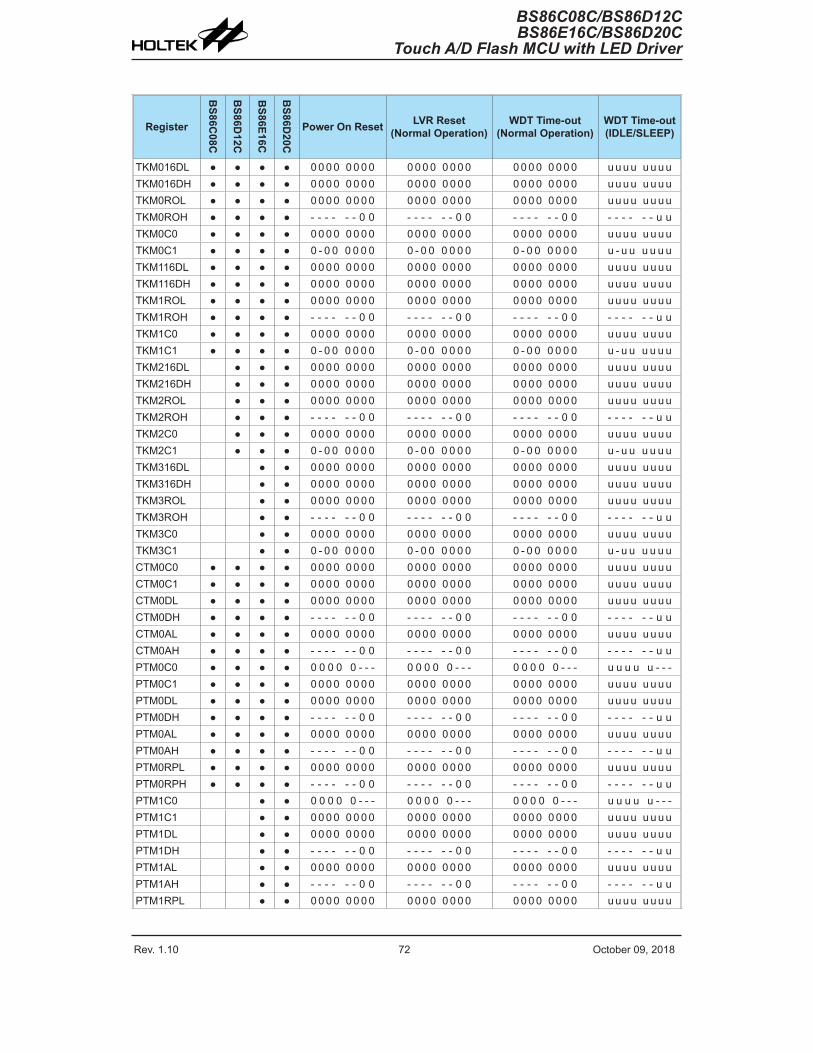
Rev. 1.10 72 October 09, 2018 Rev. 1.10 73 October 09, 2018
BS86C08C/BS86D12CBS86E16C/BS86D20C
Touch A/D Flash MCU with LED Driver
BS86C08C/BS86D12CBS86E16C/BS86D20CTouch A/D Flash MCU with LED Driver
Register
BS86C
08C
BS86D
12C
BS86E16C
BS86D
20C
Power On Reset LVR Reset(Normal Operation)
WDT Time-out (Normal Operation)
WDT Time-out (IDLE/SLEEP)
TKM016DL ● ● ● ● 0 0 0 0 0 0 0 0 0 0 0 0 0 0 0 0 0 0 0 0 0 0 0 0 u u u u u u u uTKM016DH ● ● ● ● 0 0 0 0 0 0 0 0 0 0 0 0 0 0 0 0 0 0 0 0 0 0 0 0 u u u u u u u uTKM0ROL ● ● ● ● 0 0 0 0 0 0 0 0 0 0 0 0 0 0 0 0 0 0 0 0 0 0 0 0 u u u u u u u uTKM0ROH ● ● ● ● - - - - - - 0 0 - - - - - - 0 0 - - - - - - 0 0 - - - - - - u uTKM0C0 ● ● ● ● 0 0 0 0 0 0 0 0 0 0 0 0 0 0 0 0 0 0 0 0 0 0 0 0 u u u u u u u uTKM0C1 ● ● ● ● 0 - 0 0 0 0 0 0 0 - 0 0 0 0 0 0 0 - 0 0 0 0 0 0 u - u u u u u uTKM116DL ● ● ● ● 0 0 0 0 0 0 0 0 0 0 0 0 0 0 0 0 0 0 0 0 0 0 0 0 u u u u u u u uTKM116DH ● ● ● ● 0 0 0 0 0 0 0 0 0 0 0 0 0 0 0 0 0 0 0 0 0 0 0 0 u u u u u u u uTKM1ROL ● ● ● ● 0 0 0 0 0 0 0 0 0 0 0 0 0 0 0 0 0 0 0 0 0 0 0 0 u u u u u u u uTKM1ROH ● ● ● ● - - - - - - 0 0 - - - - - - 0 0 - - - - - - 0 0 - - - - - - u uTKM1C0 ● ● ● ● 0 0 0 0 0 0 0 0 0 0 0 0 0 0 0 0 0 0 0 0 0 0 0 0 u u u u u u u uTKM1C1 ● ● ● ● 0 - 0 0 0 0 0 0 0 - 0 0 0 0 0 0 0 - 0 0 0 0 0 0 u - u u u u u uTKM216DL ● ● ● 0 0 0 0 0 0 0 0 0 0 0 0 0 0 0 0 0 0 0 0 0 0 0 0 u u u u u u u uTKM216DH ● ● ● 0 0 0 0 0 0 0 0 0 0 0 0 0 0 0 0 0 0 0 0 0 0 0 0 u u u u u u u uTKM2ROL ● ● ● 0 0 0 0 0 0 0 0 0 0 0 0 0 0 0 0 0 0 0 0 0 0 0 0 u u u u u u u uTKM2ROH ● ● ● - - - - - - 0 0 - - - - - - 0 0 - - - - - - 0 0 - - - - - - u uTKM2C0 ● ● ● 0 0 0 0 0 0 0 0 0 0 0 0 0 0 0 0 0 0 0 0 0 0 0 0 u u u u u u u uTKM2C1 ● ● ● 0 - 0 0 0 0 0 0 0 - 0 0 0 0 0 0 0 - 0 0 0 0 0 0 u - u u u u u uTKM316DL ● ● 0 0 0 0 0 0 0 0 0 0 0 0 0 0 0 0 0 0 0 0 0 0 0 0 u u u u u u u uTKM316DH ● ● 0 0 0 0 0 0 0 0 0 0 0 0 0 0 0 0 0 0 0 0 0 0 0 0 u u u u u u u uTKM3ROL ● ● 0 0 0 0 0 0 0 0 0 0 0 0 0 0 0 0 0 0 0 0 0 0 0 0 u u u u u u u uTKM3ROH ● ● - - - - - - 0 0 - - - - - - 0 0 - - - - - - 0 0 - - - - - - u uTKM3C0 ● ● 0 0 0 0 0 0 0 0 0 0 0 0 0 0 0 0 0 0 0 0 0 0 0 0 u u u u u u u uTKM3C1 ● ● 0 - 0 0 0 0 0 0 0 - 0 0 0 0 0 0 0 - 0 0 0 0 0 0 u - u u u u u uCTM0C0 ● ● ● ● 0 0 0 0 0 0 0 0 0 0 0 0 0 0 0 0 0 0 0 0 0 0 0 0 u u u u u u u uCTM0C1 ● ● ● ● 0 0 0 0 0 0 0 0 0 0 0 0 0 0 0 0 0 0 0 0 0 0 0 0 u u u u u u u uCTM0DL ● ● ● ● 0 0 0 0 0 0 0 0 0 0 0 0 0 0 0 0 0 0 0 0 0 0 0 0 u u u u u u u uCTM0DH ● ● ● ● - - - - - - 0 0 - - - - - - 0 0 - - - - - - 0 0 - - - - - - u uCTM0AL ● ● ● ● 0 0 0 0 0 0 0 0 0 0 0 0 0 0 0 0 0 0 0 0 0 0 0 0 u u u u u u u uCTM0AH ● ● ● ● - - - - - - 0 0 - - - - - - 0 0 - - - - - - 0 0 - - - - - - u uPTM0C0 ● ● ● ● 0 0 0 0 0 - - - 0 0 0 0 0 - - - 0 0 0 0 0 - - - u u u u u - - -PTM0C1 ● ● ● ● 0 0 0 0 0 0 0 0 0 0 0 0 0 0 0 0 0 0 0 0 0 0 0 0 u u u u u u u uPTM0DL ● ● ● ● 0 0 0 0 0 0 0 0 0 0 0 0 0 0 0 0 0 0 0 0 0 0 0 0 u u u u u u u uPTM0DH ● ● ● ● - - - - - - 0 0 - - - - - - 0 0 - - - - - - 0 0 - - - - - - u uPTM0AL ● ● ● ● 0 0 0 0 0 0 0 0 0 0 0 0 0 0 0 0 0 0 0 0 0 0 0 0 u u u u u u u uPTM0AH ● ● ● ● - - - - - - 0 0 - - - - - - 0 0 - - - - - - 0 0 - - - - - - u uPTM0RPL ● ● ● ● 0 0 0 0 0 0 0 0 0 0 0 0 0 0 0 0 0 0 0 0 0 0 0 0 u u u u u u u uPTM0RPH ● ● ● ● - - - - - - 0 0 - - - - - - 0 0 - - - - - - 0 0 - - - - - - u uPTM1C0 ● ● 0 0 0 0 0 - - - 0 0 0 0 0 - - - 0 0 0 0 0 - - - u u u u u - - -PTM1C1 ● ● 0 0 0 0 0 0 0 0 0 0 0 0 0 0 0 0 0 0 0 0 0 0 0 0 u u u u u u u uPTM1DL ● ● 0 0 0 0 0 0 0 0 0 0 0 0 0 0 0 0 0 0 0 0 0 0 0 0 u u u u u u u uPTM1DH ● ● - - - - - - 0 0 - - - - - - 0 0 - - - - - - 0 0 - - - - - - u uPTM1AL ● ● 0 0 0 0 0 0 0 0 0 0 0 0 0 0 0 0 0 0 0 0 0 0 0 0 u u u u u u u uPTM1AH ● ● - - - - - - 0 0 - - - - - - 0 0 - - - - - - 0 0 - - - - - - u uPTM1RPL ● ● 0 0 0 0 0 0 0 0 0 0 0 0 0 0 0 0 0 0 0 0 0 0 0 0 u u u u u u u u
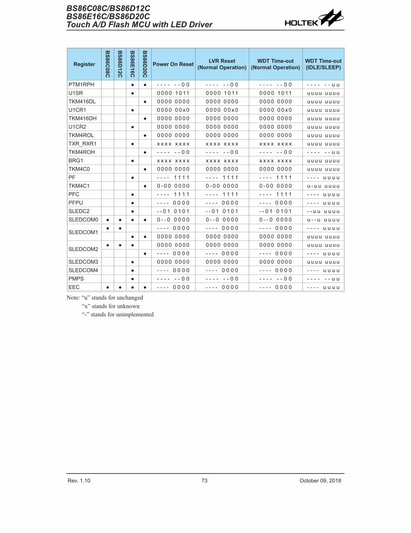
Rev. 1.10 72 October 09, 2018 Rev. 1.10 73 October 09, 2018
BS86C08C/BS86D12CBS86E16C/BS86D20C
Touch A/D Flash MCU with LED Driver
BS86C08C/BS86D12CBS86E16C/BS86D20CTouch A/D Flash MCU with LED Driver
Register
BS86C
08C
BS86D
12C
BS86E16C
BS86D
20C
Power On Reset LVR Reset(Normal Operation)
WDT Time-out (Normal Operation)
WDT Time-out (IDLE/SLEEP)
PTM1RPH ● ● - - - - - - 0 0 - - - - - - 0 0 - - - - - - 0 0 - - - - - - u uU1SR ● 0 0 0 0 1 0 11 0 0 0 0 1 0 11 0 0 0 0 1 0 11 u u u u u u u uTKM416DL ● 0 0 0 0 0 0 0 0 0 0 0 0 0 0 0 0 0 0 0 0 0 0 0 0 u u u u u u u uU1CR1 ● 0 0 0 0 0 0 x 0 0 0 0 0 0 0 x 0 0 0 0 0 0 0 x 0 u u u u u u u uTKM416DH ● 0 0 0 0 0 0 0 0 0 0 0 0 0 0 0 0 0 0 0 0 0 0 0 0 u u u u u u u uU1CR2 ● 0 0 0 0 0 0 0 0 0 0 0 0 0 0 0 0 0 0 0 0 0 0 0 0 u u u u u u u uTKM4ROL ● 0 0 0 0 0 0 0 0 0 0 0 0 0 0 0 0 0 0 0 0 0 0 0 0 u u u u u u u uTXR_RXR1 ● x x x x x x x x x x x x x x x x x x x x x x x x u u u u u u u uTKM4ROH ● - - - - - - 0 0 - - - - - - 0 0 - - - - - - 0 0 - - - - - - u uBRG1 ● x x x x x x x x x x x x x x x x x x x x x x x x u u u u u u u uTKM4C0 ● 0 0 0 0 0 0 0 0 0 0 0 0 0 0 0 0 0 0 0 0 0 0 0 0 u u u u u u u uPF ● - - - - 1 1 1 1 - - - - 1 1 1 1 - - - - 1 1 1 1 - - - - u u u uTKM4C1 ● 0 - 0 0 0 0 0 0 0 - 0 0 0 0 0 0 0 - 0 0 0 0 0 0 u - u u u u u uPFC ● - - - - 1 1 1 1 - - - - 1 1 1 1 - - - - 1 1 1 1 - - - - u u u uPFPU ● - - - - 0 0 0 0 - - - - 0 0 0 0 - - - - 0 0 0 0 - - - - u u u uSLEDC2 ● - - 0 1 0 1 0 1 - - 0 1 0 1 0 1 - - 0 1 0 1 0 1 - - u u u u u uSLEDCOM0 ● ● ● ● 0 - - 0 0 0 0 0 0 - - 0 0 0 0 0 0 - - 0 0 0 0 0 u - - u u u u u
SLEDCOM1● ● - - - - 0 0 0 0 - - - - 0 0 0 0 - - - - 0 0 0 0 - - - - u u u u
● ● 0 0 0 0 0 0 0 0 0 0 0 0 0 0 0 0 0 0 0 0 0 0 0 0 u u u u u u u u
SLEDCOM2● ● ● 0 0 0 0 0 0 0 0 0 0 0 0 0 0 0 0 0 0 0 0 0 0 0 0 u u u u u u u u
● - - - - 0 0 0 0 - - - - 0 0 0 0 - - - - 0 0 0 0 - - - - u u u uSLEDCOM3 ● 0 0 0 0 0 0 0 0 0 0 0 0 0 0 0 0 0 0 0 0 0 0 0 0 u u u u u u u uSLEDCOM4 ● - - - - 0 0 0 0 - - - - 0 0 0 0 - - - - 0 0 0 0 - - - - u u u uPMPS ● - - - - - - 0 0 - - - - - - 0 0 - - - - - - 0 0 - - - - - - u uEEC ● ● ● ● - - - - 0 0 0 0 - - - - 0 0 0 0 - - - - 0 0 0 0 - - - - u u u u
Note: “u” stands for unchanged“x” stands for unknown“-” stands for unimplemented

Rev. 1.10 74 October 09, 2018 Rev. 1.10 75 October 09, 2018
BS86C08C/BS86D12CBS86E16C/BS86D20C
Touch A/D Flash MCU with LED Driver
BS86C08C/BS86D12CBS86E16C/BS86D20CTouch A/D Flash MCU with LED Driver
Input/Output PortsHoltek microcontrollers offer considerable flexibility on their I/O ports. With the input or output designation of every pin fully under user program control, pull-high selections for all ports and wake-up selections on certain pins, the user is provided with an I/O structure to meet the needs of a wide range of application possibilities.
These devices provide bidirectional input/output lines. These I/O ports are mapped to the RAM Data Memory with specific addresses as shown in the Special Purpose Data Memory table. All of these I/O ports can be used for input and output operations. For input operation, these ports are non-latching, which means the inputs must be ready at the T2 rising edge of instruction “MOV A, [m]”, where “m” denotes the port address. For output operation, all the data is latched and remains unchanged until the output latch is rewritten.
Register Name
Bit
7 6 5 4 3 2 1 0PA PA7 — — PA4 PA3 PA2 PA1 PA0
PAC PAC7 — — PAC4 PAC3 PAC2 PAC1 PAC0PAPU PAPU7 — — PAPU4 PAPU3 PAPU2 PAPU1 PAPU0PAWU PAWU7 — — PAWU4 PAWU3 PAWU2 PAWU1 PAWU0
PB PB7 PB6 PB5 PB4 PB3 PB2 PB1 PB0PBC PBC7 PBC6 PBC5 PBC4 PBC3 PBC2 PBC1 PBC0
PBPU PBPU7 PBPU6 PBPU5 PBPU4 PBPU3 PBPU2 PBPU1 PBPU0PC — — — — PC3 PC2 PC1 PC0
PCC — — — — PCC3 PCC2 PCC1 PCC0PCPU — — — — PCPU3 PCPU2 PCPU1 PCPU0
PD PD7 PD6 PD5 PD4 PD3 PD2 PD1 PD0PDC PDC7 PDC6 PDC5 PDC4 PDC3 PDC2 PDC1 PDC0
PDPU PDPU7 PDPU6 PDPU5 PDPU4 PDPU3 PDPU2 PDPU1 PDPU0“—”: Unimplemented, read as “0”
I/O Logic Function Register List – BS86C08C/BS86D12C
Register Name
Bit
7 6 5 4 3 2 1 0PA PA7 — — PA4 PA3 PA2 PA1 PA0
PAC PAC7 — — PAC4 PAC3 PAC2 PAC1 PAC0PAPU PAPU7 — — PAPU4 PAPU3 PAPU2 PAPU1 PAPU0PAWU PAWU7 — — PAWU4 PAWU3 PAWU2 PAWU1 PAWU0
PB PB7 PB6 PB5 PB4 PB3 PB2 PB1 PB0PBC PBC7 PBC6 PBC5 PBC4 PBC3 PBC2 PBC1 PBC0
PBPU PBPU7 PBPU6 PBPU5 PBPU4 PBPU3 PBPU2 PBPU1 PBPU0PC PC7 PC6 PC5 PC4 PC3 PC2 PC1 PC0
PCC PCC7 PCC6 PCC5 PCC4 PCC3 PCC2 PCC1 PCC0PCPU PCPU7 PCPU6 PCPU5 PCPU4 PCPU3 PCPU2 PCPU1 PCPU0
PD PD7 PD6 PD5 PD4 PD3 PD2 PD1 PD0PDC PDC7 PDC6 PDC5 PDC4 PDC3 PDC2 PDC1 PDC0
PDPU PDPU7 PDPU6 PDPU5 PDPU4 PDPU3 PDPU2 PDPU1 PDPU0PE PE7 PE6 PE5 PE4 PE3 PE2 PE1 PE0
PEC PEC7 PEC6 PEC5 PEC4 PEC3 PEC2 PEC1 PEC0PEPU PEPU7 PEPU6 PEPU5 PEPU4 PEPU3 PEPU2 PEPU1 PEPU0
PF — — — — PF3 PF2 PF1 PF0PFC — — — — PFC3 PFC2 PFC1 PFC0
PFPU — — — — PFPU3 PFPU2 PFPU1 PFPU0“—”: Unimplemented, read as “0”
I/O Logic Function Register List – BS86E16C

Rev. 1.10 74 October 09, 2018 Rev. 1.10 75 October 09, 2018
BS86C08C/BS86D12CBS86E16C/BS86D20C
Touch A/D Flash MCU with LED Driver
BS86C08C/BS86D12CBS86E16C/BS86D20CTouch A/D Flash MCU with LED Driver
Register Name
Bit
7 6 5 4 3 2 1 0PA PA7 — — PA4 PA3 PA2 PA1 PA0
PAC PAC7 — — PAC4 PAC3 PAC2 PAC1 PAC0PAPU PAPU7 — — PAPU4 PAPU3 PAPU2 PAPU1 PAPU0PAWU PAWU7 — — PAWU4 PAWU3 PAWU2 PAWU1 PAWU0
PB PB7 PB6 PB5 PB4 PB3 PB2 PB1 PB0PBC PBC7 PBC6 PBC5 PBC4 PBC3 PBC2 PBC1 PBC0
PBPU PBPU7 PBPU6 PBPU5 PBPU4 PBPU3 PBPU2 PBPU1 PBPU0PC PC7 PC6 PC5 PC4 PC3 PC2 PC1 PC0
PCC PCC7 PCC6 PCC5 PCC4 PCC3 PCC2 PCC1 PCC0PCPU PCPU7 PCPU6 PCPU5 PCPU4 PCPU3 PCPU2 PCPU1 PCPU0
PD — — — — PD3 PD2 PD1 PD0PDC — — — — PDC3 PDC2 PDC1 PDC0
PDPU — — — — PDPU3 PDPU2 PDPU1 PDPU0
“—”: Unimplemented, read as “0”I/O Logic Function Register List – BS86D20C
Pull-high ResistorsMany product applications require pull-high resistors for their switch inputs usually requiring the use of an external resistor. To eliminate the need for these external resistors, all I/O pins, when configured as an input have the capability of being connected to an internal pull-high resistor. These pull-high resistors are selected using the relevant pull-high control registers and are implemented using weak PMOS transistors.
• PxPU Register
Bit 7 6 5 4 3 2 1 0Name PxPU7 PxPU6 PxPU5 PxPU4 PxPU3 PxPU2 PxPU1 PxPU0R/W R/W R/W R/W R/W R/W R/W R/W R/WPOR 0 0 0 0 0 0 0 0
PxPUn: I/O Port x Pin pull-high function control0: Disable1: Enable
The PxPUn bit is used to control the pin pull-high function. Here the “x” is the Port name which can be A, B, C, D, E and F depending upon the selected device. However, the actual available bits for each I/O Port may be different.
Port A Wake-upThe HALT instruction forces the microcontroller into the SLEEP or IDLE Mode which preserves power, a feature that is important for battery and other low-power applications. Various methods exist to wake-up the microcontroller, one of which is to change the logic condition on one of the Port A pins from high to low. This function is especially suitable for applications that can be woken up via external switches. Each pin on Port A can be selected individually to have this wake-up feature using the PAWU register.

Rev. 1.10 76 October 09, 2018 Rev. 1.10 77 October 09, 2018
BS86C08C/BS86D12CBS86E16C/BS86D20C
Touch A/D Flash MCU with LED Driver
BS86C08C/BS86D12CBS86E16C/BS86D20CTouch A/D Flash MCU with LED Driver
• PAWU Register
Bit 7 6 5 4 3 2 1 0Name PAWU7 — — PAWU4 PAWU3 PAWU2 PAWU1 PAWU0R/W R/W — — R/W R/W R/W R/W R/WPOR 0 — — 0 0 0 0 0
Bit 7, 4~0 PAWU7, PAWU4~PAWU0: Port A pin Wake-up function control0: Disable1: Enable
Bit 6~5 Unimplemented, read as “0”
I/O Port Control RegistersEach I/O Port has its own control register which controls the input/output configuration. With this control register, each I/O pin with or without pull-high resistors can be reconfigured dynamically under software control. For the I/O pin to function as an input, the corresponding bit of the control register must be written as a “1”. This will then allow the logic state of the input pin to be directly read by instructions. When the corresponding bit of the control register is written as a “0”, the I/O pin will be setup as a CMOS output. If the pin is currently setup as an output, instructions can still be used to read the output register. However, it should be noted that the program will in fact only read the status of the output data latch and not the actual logic status of the output pin.
• PxC Register
Bit 7 6 5 4 3 2 1 0Name PxC7 PxC6 PxC5 PxC4 PxC3 PxC2 PxC1 PxC0R/W R/W R/W R/W R/W R/W R/W R/W R/WPOR 1 1 1 1 1 1 1 1
PxCn: I/O Port x Pin type selection0: Output1: Input
The PxCn bit is used to control the pin type selection. Here the “x” is the Port name which can be A, B, C, D, E and F depending upon the selected device. However, the actual available bits for each I/O Port may be different.
I/O Port Source Current SelectionThese devices support different output source current driving capability for each I/O port. With the selection register, SLEDCn, specific I/O port can support four levels of the source current driving capability. These source current selection bits are available when the corresponding pin is configured as a CMOS output. Otherwise, these select bits have no effect. Users should refer to the Input/Output Characteristics section to select the desired output source current for different applications.
Register Name
Bit
7 6 5 4 3 2 1 0SLEDC0 PBPS3 PBPS2 PBPS1 PBPS0 PAPS3 PAPS2 PAPS1 PAPS0SLEDC1 PDPS3 PDPS2 PDPS1 PDPS0 — — PCPS1 PCPS0
I/O Port Source Current Selection Register List – BS86C08C/BS86D12C

Rev. 1.10 76 October 09, 2018 Rev. 1.10 77 October 09, 2018
BS86C08C/BS86D12CBS86E16C/BS86D20C
Touch A/D Flash MCU with LED Driver
BS86C08C/BS86D12CBS86E16C/BS86D20CTouch A/D Flash MCU with LED Driver
Register Name
Bit
7 6 5 4 3 2 1 0SLEDC0 PBPS3 PBPS2 PBPS1 PBPS0 PAPS3 PAPS2 PAPS1 PAPS0SLEDC1 PDPS3 PDPS2 PDPS1 PDPS0 PCPS3 PCPS2 PCPS1 PCPS0SLEDC2 — — PFPS1 PFPS0 PEPS3 PEPS2 PEPS1 PEPS0
I/O Port Source Current Selection Register List – BS86E16C
Register Name
Bit
7 6 5 4 3 2 1 0SLEDC0 PBPS3 PBPS2 PBPS1 PBPS0 PAPS3 PAPS2 PAPS1 PAPS0SLEDC1 — — PDPS1 PDPS0 PCPS3 PCPS2 PCPS1 PCPS0
I/O Port Source Current Selection Register List – BS86D20C
• SLEDC0 Register
Bit 7 6 5 4 3 2 1 0Name PBPS3 PBPS2 PBPS1 PBPS0 PAPS3 PAPS2 PAPS1 PAPS0R/W R/W R/W R/W R/W R/W R/W R/W R/WPOR 0 1 0 1 0 1 0 1
Bit 7~6 PBPS3~PBPS2: PB7~PB4 source current selection00: Source current=Level 0 (Min.)01: Source current=Level 110: Source current=Level 211: Source current=Level 3 (Max.)
Bit 5~4 PBPS1~PBPS0: PB3~PB0 source current selection00: Source current=Level 0 (Min.)01: Source current=Level 110: Source current=Level 211: Source current=Level 3 (Max.)
Bit 3~2 PAPS3~PAPS2: PA7 and PA4 source current selection00: Source current=Level 0 (Min.)01: Source current=Level 110: Source current=Level 211: Source current=Level 3 (Max.)
Bit 1~0 PAPS1~PAPS0: PA3~PA0 source current selection00: Source current=Level 0 (Min.)01: Source current=Level 110: Source current=Level 211: Source current=Level 3 (Max.)
• SLEDC1 Register – BS86C08C/BS86D12C
Bit 7 6 5 4 3 2 1 0Name PDPS3 PDPS2 PDPS1 PDPS0 — — PCPS1 PCPS0R/W R/W R/W R/W R/W — — R/W R/WPOR 0 1 0 1 — — 0 1
Bit 7~6 PDPS3~PDPS2: PD7~PD4 source current selection00: Source current=Level 0 (Min.)01: Source current=Level 110: Source current=Level 211: Source current=Level 3 (Max.)

Rev. 1.10 78 October 09, 2018 Rev. 1.10 79 October 09, 2018
BS86C08C/BS86D12CBS86E16C/BS86D20C
Touch A/D Flash MCU with LED Driver
BS86C08C/BS86D12CBS86E16C/BS86D20CTouch A/D Flash MCU with LED Driver
Bit 5~4 PDPS1~PDPS0: PD3~PD0 source current selection00: Source current=Level 0 (Min.)01: Source current=Level 110: Source current=Level 211: Source current=Level 3 (Max.)
Bit 3~2 Unimplemented, read as “0”Bit 1~0 PCPS1~PCPS0: PC3~PC0 source current selection
00: Source current=Level 0 (Min.)01: Source current=Level 110: Source current=Level 211: Source current=Level 3 (Max.)
• SLEDC1 Register – BS86E16C
Bit 7 6 5 4 3 2 1 0Name PDPS3 PDPS2 PDPS1 PDPS0 PCPS3 PCPS2 PCPS1 PCPS0R/W R/W R/W R/W R/W R/W R/W R/W R/WPOR 0 1 0 1 0 1 0 1
Bit 7~6 PDPS3~PDPS2: PD7~PD4 source current selection00: Source current=Level 0 (Min.)01: Source current=Level 110: Source current=Level 211: Source current=Level 3 (Max.)
Bit 5~4 PDPS1~PDPS0: PD3~PD0 source current selection00: Source current=Level 0 (Min.)01: Source current=Level 110: Source current=Level 211: Source current=Level 3 (Max.)
Bit 3~2 PCPS3~PCPS2: PC7~PC4 source current selection00: Source current=Level 0 (Min.)01: Source current=Level 110: Source current=Level 211: Source current=Level 3 (Max.)
Bit 1~0 PCPS1~PCPS0: PC3~PC0 source current selection00: Source current=Level 0 (Min.)01: Source current=Level 110: Source current=Level 211: Source current=Level 3 (Max.)
• SLEDC1 Register – BS86D20C
Bit 7 6 5 4 3 2 1 0Name — — PDPS1 PDPS0 PCPS3 PCPS2 PCPS1 PCPS0R/W — — R/W R/W R/W R/W R/W R/WPOR — — 0 1 0 1 0 1
Bit 7~6 Unimplemented, read as “0”Bit 5~4 PDPS1~PDPS0: PD3~PD0 source current selection
00: Source current = Level 0 (Min.)01: Source current = Level 110: Source current = Level 211: Source current = Level 3 (Max.)
Bit 3~2 PCPS3~PCPS2: PC7~PC4 source current selection00: Source current = Level 0 (Min.)01: Source current = Level 110: Source current = Level 211: Source current = Level 3 (Max.)

Rev. 1.10 78 October 09, 2018 Rev. 1.10 79 October 09, 2018
BS86C08C/BS86D12CBS86E16C/BS86D20C
Touch A/D Flash MCU with LED Driver
BS86C08C/BS86D12CBS86E16C/BS86D20CTouch A/D Flash MCU with LED Driver
Bit 1~0 PCPS1~PCPS0: PC3~PC0 source current selection00: Source current = Level 0 (Min.)01: Source current = Level 110: Source current = Level 211: Source current = Level 3 (Max.)
• SLEDC2 Register – BS86E16C
Bit 7 6 5 4 3 2 1 0Name — — PFPS1 PFPS0 PEPS3 PEPS2 PEPS1 PEPS0R/W — — R/W R/W R/W R/W R/W R/WPOR — — 0 1 0 1 0 1
Bit 7~6 Unimplemented, read as “0”Bit 5~4 PFPS1~PFPS0: PF3~PF0 source current selection
00: Source current=Level 0 (Min.)01: Source current=Level 110: Source current=Level 211: Source current=Level 3 (Max.)
Bit 3~2 PEPS3~PEPS2: PE7~PE4 source current selection00: Source current=Level 0 (Min.)01: Source current=Level 110: Source current=Level 211: Source current=Level 3 (Max.)
Bit 1~0 PEPS1~PEPS0: PE3~PE0 source current selection00: Source current=Level 0 (Min.)01: Source current=Level 110: Source current=Level 211: Source current=Level 3 (Max.)
I/O Port Sink Current SelectionThese devices support different output sink current driving capability for PA, PC, PD, PE and PF ports. With the selection register, SLEDCOMn, specific I/O port can support two levels of the sink current driving capability. These sink current selection bits are available when the corresponding pin is configured as a CMOS output. Otherwise, these select bits have no effect. Users should refer to the Input/Output Characteristics section to select the desired output sink current for different applications.
Register Name
Bit
7 6 5 4 3 2 1 0SLEDCOM0 PANS7 — — PANS4 PANS3 PANS2 PANS1 PANS0SLEDCOM1 — — — — PCNS3 PCNS2 PCNS1 PCNS0SLEDCOM2 PDNS7 PDNS6 PDNS5 PDNS4 PDNS3 PDNS2 PDNS1 PDNS0
I/O Port Sink Current Selection Register List – BS86C08C/BS86D12C
Register Name
Bit
7 6 5 4 3 2 1 0SLEDCOM0 PANS7 — — PANS4 PANS3 PANS2 PANS1 PANS0SLEDCOM1 PCNS7 PCNS6 PCNS5 PCNS4 PCNS3 PCNS2 PCNS1 PCNS0SLEDCOM2 PDNS7 PDNS6 PDNS5 PDNS4 PDNS3 PDNS2 PDNS1 PDNS0SLEDCOM3 PENS7 PENS6 PENS5 PENS4 PENS3 PENS2 PENS1 PENS0SLEDCOM4 — — — — PFNS3 PFNS2 PFNS1 PFNS0
I/O Port Sink Current Selection Register List – BS86E16C

Rev. 1.10 80 October 09, 2018 Rev. 1.10 81 October 09, 2018
BS86C08C/BS86D12CBS86E16C/BS86D20C
Touch A/D Flash MCU with LED Driver
BS86C08C/BS86D12CBS86E16C/BS86D20CTouch A/D Flash MCU with LED Driver
Register Name
Bit
7 6 5 4 3 2 1 0SLEDCOM0 PANS7 — — PANS4 PANS3 PANS2 PANS1 PANS0SLEDCOM1 PCNS7 PCNS6 PCNS5 PCNS4 PCNS3 PCNS2 PCNS1 PCNS0SLEDCOM2 — — — — PDNS3 PDNS2 PDNS1 PDNS0
I/O Port Sink Current Selection Register List – BS86D20C
• SLEDCOM0 Register
Bit 7 6 5 4 3 2 1 0Name PANS7 — — PANS4 PANS3 PANS2 PANS1 PANS0R/W R/W — — R/W R/W R/W R/W R/WPOR 0 — — 0 0 0 0 0
Bit 7 PANS7: PA7 sink current selection0: Sink current=Level 0 (Min.)1: Sink current=Level 1 (Max.)
Bit 6~5 Unimplemented, read as “0”Bit 4 PANS4: PA4 sink current selection
0: Sink current=Level 0 (Min.)1: Sink current=Level 1 (Max.)
Bit 3 PANS3: PA3 sink current selection0: Sink current=Level 0 (Min.)1: Sink current=Level 1 (Max.)
Bit 2 PANS2: PA2 sink current selection0: Sink current=Level 0 (Min.)1: Sink current=Level 1 (Max.)
Bit 1 PANS1: PA1 sink current selection0: Sink current=Level 0 (Min.)1: Sink current=Level 1 (Max.)
Bit 0 PANS0: PA0 sink current selection0: Sink current=Level 0 (Min.)1: Sink current=Level 1 (Max.)
• SLEDCOM1 Register – BS86C08C/BS86D12C
Bit 7 6 5 4 3 2 1 0Name — — — — PCNS3 PCNS2 PCNS1 PCNS0R/W — — — — R/W R/W R/W R/WPOR — — — — 0 0 0 0
Bit 7~4 Unimplemented, read as “0”Bit 3 PCNS3: PC3 sink current selection
0: Sink current=Level 0 (Min.)1: Sink current=Level 1 (Max.)
Bit 2 PCNS2: PC2 sink current selection0: Sink current=Level 0 (Min.)1: Sink current=Level 1 (Max.)
Bit 1 PCNS1: PC1 sink current selection0: Sink current=Level 0 (Min.)1: Sink current=Level 1 (Max.)
Bit 0 PCNS0: PC0 sink current selection0: Sink current=Level 0 (Min.)1: Sink current=Level 1 (Max.)

Rev. 1.10 80 October 09, 2018 Rev. 1.10 81 October 09, 2018
BS86C08C/BS86D12CBS86E16C/BS86D20C
Touch A/D Flash MCU with LED Driver
BS86C08C/BS86D12CBS86E16C/BS86D20CTouch A/D Flash MCU with LED Driver
• SLEDCOM1 Register – BS86E16C/BS86D20C
Bit 7 6 5 4 3 2 1 0Name PCNS7 PCNS6 PCNS5 PCNS4 PCNS3 PCNS2 PCNS1 PCNS0R/W R/W R/W R/W R/W R/W R/W R/W R/WPOR 0 0 0 0 0 0 0 0
Bit 7 PCNS7: PC7 sink current selection0: Sink current=Level 0 (Min.)1: Sink current=Level 1 (Max.)
Bit 6 PCNS6: PC6 sink current selection0: Sink current=Level 0 (Min.)1: Sink current=Level 1 (Max.)
Bit 5 PCNS5: PC5 sink current selection0: Sink current=Level 0 (Min.)1: Sink current=Level 1 (Max.)
Bit 4 PCNS4: PC4 sink current selection0: Sink current=Level 0 (Min.)1: Sink current=Level 1 (Max.)
Bit 3 PCNS3: PC3 sink current selection0: Sink current=Level 0 (Min.)1: Sink current=Level 1 (Max.)
Bit 2 PCNS2: PC2 sink current selection0: Sink current=Level 0 (Min.)1: Sink current=Level 1 (Max.)
Bit 1 PCNS1: PC1 sink current selection0: Sink current=Level 0 (Min.)1: Sink current=Level 1 (Max.)
Bit 0 PCNS0: PC0 sink current selection0: Sink current=Level 0 (Min.)1: Sink current=Level 1 (Max.)
• SLEDCOM2 Register –BS86C08C/BS86D12C/BS86E16C
Bit 7 6 5 4 3 2 1 0Name PDNS7 PDNS6 PDNS5 PDNS4 PDNS3 PDNS2 PDNS1 PDNS0R/W R/W R/W R/W R/W R/W R/W R/W R/WPOR 0 0 0 0 0 0 0 0
Bit 7 PDNS7: PD7 sink current selection0: Sink current=Level 0 (Min.)1: Sink current=Level 1 (Max.)
Bit 6 PDNS6: PD6 sink current selection0: Sink current=Level 0 (Min.)1: Sink current=Level 1 (Max.)
Bit 5 PDNS5: PD5 sink current selection0: Sink current=Level 0 (Min.)1: Sink current=Level 1 (Max.)
Bit 4 PDNS4: PD4 sink current selection0: Sink current=Level 0 (Min.)1: Sink current=Level 1 (Max.)
Bit 3 PDNS3: PD3 sink current selection0: Sink current=Level 0 (Min.)1: Sink current=Level 1 (Max.)

Rev. 1.10 82 October 09, 2018 Rev. 1.10 83 October 09, 2018
BS86C08C/BS86D12CBS86E16C/BS86D20C
Touch A/D Flash MCU with LED Driver
BS86C08C/BS86D12CBS86E16C/BS86D20CTouch A/D Flash MCU with LED Driver
Bit 2 PDNS2: PD2 sink current selection0: Sink current=Level 0 (Min.)1: Sink current=Level 1 (Max.)
Bit 1 PDNS1: PD1 sink current selection0: Sink current=Level 0 (Min.)1: Sink current=Level 1 (Max.)
Bit 0 PDNS0: PD0 sink current selection0: Sink current=Level 0 (Min.)1: Sink current=Level 1 (Max.)
• SLEDCOM2 Register – BS86D20C
Bit 7 6 5 4 3 2 1 0Name — — — — PDNS3 PDNS2 PDNS1 PDNS0R/W — — — — R/W R/W R/W R/WPOR — — — — 0 0 0 0
Bit 7~4 Unimplemented, read as “0”Bit 3 PDNS3: PD3 sink current selection
0: Sink current=Level 0 (Min.)1: Sink current=Level 1 (Max.)
Bit 2 PDNS2: PD2 sink current selection0: Sink current=Level 0 (Min.)1: Sink current=Level 1 (Max.)
Bit 1 PDNS1: PD1 sink current selection0: Sink current=Level 0 (Min.)1: Sink current=Level 1 (Max.)
Bit 0 PDNS0: PD0 sink current selection0: Sink current=Level 0 (Min.)1: Sink current=Level 1 (Max.)
• SLEDCOM3 Register – BS86E16C
Bit 7 6 5 4 3 2 1 0Name PENS7 PENS6 PENS5 PENS4 PENS3 PENS2 PENS1 PENS0R/W R/W R/W R/W R/W R/W R/W R/W R/WPOR 0 0 0 0 0 0 0 0
Bit 7 PENS7: PE7 sink current selection0: Sink current=Level 0 (Min.)1: Sink current=Level 1 (Max.)
Bit 6 PENS6: PE6 sink current selection0: Sink current=Level 0 (Min.)1: Sink current=Level 1 (Max.)
Bit 5 PENS5: PE5 sink current selection0: Sink current=Level 0 (Min.)1: Sink current=Level 1 (Max.)
Bit 4 PENS4: PE4 sink current selection0: Sink current=Level 0 (Min.)1: Sink current=Level 1 (Max.)
Bit 3 PENS3: PE3 sink current selection0: Sink current=Level 0 (Min.)1: Sink current=Level 1 (Max.)
Bit 2 PENS2: PE2 sink current selection0: Sink current=Level 0 (Min.)1: Sink current=Level 1 (Max.)

Rev. 1.10 82 October 09, 2018 Rev. 1.10 83 October 09, 2018
BS86C08C/BS86D12CBS86E16C/BS86D20C
Touch A/D Flash MCU with LED Driver
BS86C08C/BS86D12CBS86E16C/BS86D20CTouch A/D Flash MCU with LED Driver
Bit 1 PENS1: PE1 sink current selection0: Sink current=Level 0 (Min.)1: Sink current=Level 1 (Max.)
Bit 0 PENS0: PE0 sink current selection0: Sink current=Level 0 (Min.)1: Sink current=Level 1 (Max.)
• SLEDCOM4 Register – BS86E16C
Bit 7 6 5 4 3 2 1 0Name — — — — PFNS3 PFNS2 PFNS1 PFNS0R/W — — — — R/W R/W R/W R/WPOR — — — — 0 0 0 0
Bit 7~4 Unimplemented, read as “0”Bit 3 PFNS3: PF3 sink current selection
0: Sink current=Level 0 (Min.)1: Sink current=Level 1 (Max.)
Bit 2 PFNS2: PF2 sink current selection0: Sink current=Level 0 (Min.)1: Sink current=Level 1 (Max.)
Bit 1 PFNS1: PF1 sink current selection0: Sink current=Level 0 (Min.)1: Sink current=Level 1 (Max.)
Bit 0 PFNS0: PF0 sink current selection0: Sink current=Level 0 (Min.)1: Sink current=Level 1 (Max.)
I/O Port Power Source Control – BS86E16C OnlyThe BS86E16C device supports different I/O port power source selections for PD7~PD6 pins. The port power can come from either the power pin VDD or VDDIO which is determined by using the PMPS1~PMPS0 bits in the PMPS register. An important point to know is that the input power voltage on the VDDIO pin should be equal to or less than the device supply power voltage when the VDDIO pin is selected as the port power supply pin.
With the exception of OCDS, the multi-power function is only effective when the pin is set to have a digital input or output function.
• PMPS Register
Bit 7 6 5 4 3 2 1 0Name — — — — — — PMPS1 PMPS0R/W — — — — — — R/W R/WPOR — — — — — — 0 0
Bit 7~2 Unimplemented, read as “0”Bit 1~0 PMPS1~PMPS0: PD7~PD6 pin power source selection
0x: VDD1x: VDDIO
Pin-remapping FunctionThe flexibility of the microcontroller range is greatly enhanced by the use of pins that have more than one function. Limited numbers of pins can force serious design constraints on designers but by supplying pins with multi-functions, many of these difficulties can be overcome. The way in which the pin function of specific pins is selected is different for each function and a priority order is established where more than one pin function is selected simultaneously.

Rev. 1.10 84 October 09, 2018 Rev. 1.10 85 October 09, 2018
BS86C08C/BS86D12CBS86E16C/BS86D20C
Touch A/D Flash MCU with LED Driver
BS86C08C/BS86D12CBS86E16C/BS86D20CTouch A/D Flash MCU with LED Driver
Pin-remapping Selection RegisterThe limited number of supplied pins in a package can impose restrictions on the amount of functions a certain device can contain. However by allowing the same pins to share several different functions and providing a means of function selection, a wide range of different functions can be incorporated into even relatively small package sizes.
Register Name
Bit
7 6 5 4 3 2 1 0IFS0 SDAPS1 SDAPS0 SCLPS1 SCLPS0 TX0PS1 TX0PS0 RX0PS1 RX0PS0IFS1 — — — — — CTCK0PS — CTP0PSIFS2 — RX0EN — — — — — —
Pin-remapping Selection Register List – BS86C08C/BS86D12C
Register Name
Bit
7 6 5 4 3 2 1 0IFS0 SDAPS1 SDAPS0 SCLPS1 SCLPS0 TX0PS1 TX0PS0 RX0PS1 RX0PS0IFS1 PTP1PS PTP1IPS PTP0PS CTP0BPS CTCK0PS1 CTCK0PS0 CTP0PS1 CTP0PS0IFS2 RX1EN RX0EN TX1PS1 TX1PS0 RX1PS1 RX1PS0 PTP1BPS PTCK1PS
Pin-remapping Selection Register List – BS86E16C
Register Name
Bit
7 6 5 4 3 2 1 0IFS0 SDOPS SCSBPS SDIPS SCKPS TX0PS1 TX0PS0 RX0PS1 RX0PS0IFS1 — — — — — RX0EN PTCK0PS PTP0IPS
Pin-remapping Selection Register List – BS86D20C
• IFS0 Register – BS86C08C/BS86D12C
Bit 7 6 5 4 3 2 1 0Name SDAPS1 SDAPS0 SCLPS1 SCLPS0 TX0PS1 TX0PS0 RX0PS1 RX0PS0R/W R/W R/W R/W R/W R/W R/W R/W R/WPOR 0 0 0 0 0 0 0 0
Bit 7~6 SDAPS1~SDAPS0: SDA pin remapping function selection00: SDA on PD701: SDA on PA310: SDA on PC311: SDA on PD7
Bit 5~4 SCLPS1~SCLPS0: SCL pin remapping function selection00: SCL on PD601: SCL on PA110: SCL on PC211: SCL on PD6
Bit 3~2 TX0PS1~TX0PS0: TX0 pin remapping function selection00: TX0 on PA3 01: TX0 on PA310: TX0 on PC311: TX0 on PD7
Bit 1~0 RX0PS1~RX0PS0: RX0 pin remapping function selection00: RX0 on PA101: RX0 on PA110: RX0 on PC211: RX0 on PD6

Rev. 1.10 84 October 09, 2018 Rev. 1.10 85 October 09, 2018
BS86C08C/BS86D12CBS86E16C/BS86D20C
Touch A/D Flash MCU with LED Driver
BS86C08C/BS86D12CBS86E16C/BS86D20CTouch A/D Flash MCU with LED Driver
• IFS0 Register – BS86E16C
Bit 7 6 5 4 3 2 1 0Name SDAPS1 SDAPS0 SCLPS1 SCLPS0 TX0PS1 TX0PS0 RX0PS1 RX0PS0R/W R/W R/W R/W R/W R/W R/W R/W R/WPOR 0 0 0 0 0 0 0 0
Bit 7~6 SDAPS1~SDAPS0: SDA pin remapping function selection00: SDA on PD701: SDA on PA310: SDA on PC311: SDA on PC7
Bit 5~4 SCLPS1~SCLPS0: SCL pin remapping function selection00: SCL on PD601: SCL on PA110: SCL on PC211: SCL on PC6
Bit 3~2 TX0PS1~TX0PS0: TX0 pin remapping function selection00: TX0 on PA301: TX0 on PE110: TX0 on PC311: TX0 on PD7
Bit 1~0 RX0PS1~RX0PS0: RX0 pin remapping function selection00: RX0 on PA101: RX0 on PE010: RX0 on PC211: RX0 on PD6
• IFS0 Register – BS86D20C
Bit 7 6 5 4 3 2 1 0Name SDOPS SCSBPS SDIPS SCKPS TX0PS1 TX0PS0 RX0PS1 RX0PS0R/W R/W R/W R/W R/W R/W R/W R/W R/WPOR 0 0 0 0 0 0 0 0
Bit 7 SDOPS: SDO pin remapping function selection0: SDO on PA01: SDO on PC5
Bit 6 SCSBPS: SCS pin remapping function selection0: SCS on PA21: SCS on PC4
Bit 5 SDIPS: SDI/SDA pin remapping function selection0: SDI/SDA on PA31: SDI/SDA on PA1
Bit 4 SCKPS: SCK/SCL pin remapping function selection0: SCK/SCL on PA71: SCK/SCL on PA4
Bit 3~2 TX0PS1~TX0PS0: TX0 pin remapping function selection00: TX0 on PA701: TX0 on PD110: TX0 on PA111: TX0 on PA7
Bit 1~0 RX0PS1~RX0PS0: RX0 pin remapping function selection00: RX0 on PA301: RX0 on PD010: RX0 on PA411: RX0 on PA3

Rev. 1.10 86 October 09, 2018 Rev. 1.10 87 October 09, 2018
BS86C08C/BS86D12CBS86E16C/BS86D20C
Touch A/D Flash MCU with LED Driver
BS86C08C/BS86D12CBS86E16C/BS86D20CTouch A/D Flash MCU with LED Driver
• IFS1 Register – BS86C08C/BS86D12C
Bit 7 6 5 4 3 2 1 0Name — — — — — CTCK0PS — CTP0PSR/W — — — — — R/W — R/WPOR — — — — — 0 — 0
Bit 7~3 Unimplemented, read as “0”Bit 2 CTCK0PS: CTCK0 pin remapping function selection
0: CTCK0 on PA71: CTCK0 on PC0
Bit 1 Unimplemented, read as “0”Bit 0 CTP0: CTP0 pin remapping function selection
0: CTP0 on PA41: CTP0 on PC1
• IFS1 Register – BS86E16C
Bit 7 6 5 4 3 2 1 0Name PTP1PS PTP1IPS PTP0PS CTP0BPS CTCK0PS1 CTCK0PS0 CTP0PS1 CTP0PS0R/W R/W R/W R/W R/W R/W R/W R/W R/WPOR 0 0 0 0 0 0 0 0
Bit 7 PTP1PS: PTP1 pin remapping function selection0: PTP1 on PE41: PTP1 on PD3
Bit 6 PTP1IPS: PTP1I pin remapping function selection0: PTP1I on PE61: PTP1I on PD2
Bit 5 PTP0PS: PTP0 pin remapping function selection0: PTP0 on PF31: PTP0 on PD5
Bit 4 CTP0BPS: CTP0B pin remapping function selection0: CTP0B on PF21: CTP0B on PA0
Bit 3~2 CTCK0PS1~CTCK0PS0: CTCK0 pin remapping function selection00: CTCK0 on PA701: CTCK0 on PC010: CTCK0 on PF111: CTCK0 on PA7
Bit 1~0 CTP0PS1~CTP0PS0: CTP0 pin remapping function selection00: CTP0 on PA401: CTP0 on PC110: CTP0 on PF011: CTP0 on PA4
• IFS1 Register – BS86D20C
Bit 7 6 5 4 3 2 1 0Name — — — — — RX0EN PTCK0PS PTP0IPSR/W — — — — — R/W R/W R/WPOR — — — — — 0 0 0
Bit 7~3 Unimplemented, read as "0"Bit 2 RX0EN: RX0 input enable control
0: Disable1: Enable

Rev. 1.10 86 October 09, 2018 Rev. 1.10 87 October 09, 2018
BS86C08C/BS86D12CBS86E16C/BS86D20C
Touch A/D Flash MCU with LED Driver
BS86C08C/BS86D12CBS86E16C/BS86D20CTouch A/D Flash MCU with LED Driver
Bit 1 PTCK0PS: PTCK0 pin remapping function selection0: PTCK0 on PA01: PTCK0 on PC2
Bit 0 PTP0IPS: PTP0I pin remapping function selection0: PTP0I on PA21: PTP0I on PC3
• IFS2 Register – BS86C08C/BS86D12C
Bit 7 6 5 4 3 2 1 0Name — RX0EN — — — — — —R/W — R/W — — — — — —POR — 0 — — — — — —
Bit 7 Unimplemented, read as “0”Bit 6 RX0EN: RX0 input enable control
0: Disable1: Enable
Bit 5~0 Unimplemented, read as “0”
• IFS2 Register – BS86E16C
Bit 7 6 5 4 3 2 1 0Name RX1EN RX0EN TX1PS1 TX1PS0 RX1PS1 RX1PS0 PTP1BPS PTCK1PSR/W R/W R/W R/W R/W R/W R/W R/W R/WPOR 0 0 0 0 0 0 0 0
Bit 7 RX1EN: RX1 input enable control0: Disable1: Enable
Bit 6 RX0EN: RX0 input enable control0: Disable1: Enable
Bit 5~4 TX1PS1~TX1PS0: TX1 pin remapping function selection00: TX1 on PF101: TX1 on PE310: TX1 on PD311: TX1 on PA7
Bit 3~2 RX1PS1~RX1PS0: RX1 pin remapping function selection00: RX1 on PF001: RX1 on PE210: RX1 on PD211: RX1 on PA4
Bit 1 PTP1BPS: PTP1B pin remapping function selection0: PTP1B on PE51: PTP1B on PE3
Bit 0 PTCK1PS: PTCK1 pin remapping function selection0: PTCK1 on PE71: PTCK1 on PD4
I/O Pin StructuresThe accompanying diagram illustrates the internal structure of the I/O logic function. As the exact logical construction of the I/O pin will differ from this drawing, it is supplied as a guide only to assist with the functional understanding of the I/O logic function. The wide range of pin-shared structures does not permit all types to be shown.

Rev. 1.10 88 October 09, 2018 Rev. 1.10 89 October 09, 2018
BS86C08C/BS86D12CBS86E16C/BS86D20C
Touch A/D Flash MCU with LED Driver
BS86C08C/BS86D12CBS86E16C/BS86D20CTouch A/D Flash MCU with LED Driver
MUX
VDD
Control Bit
Data Bit
Data Bus
Write Control Register
Chip Reset
Read Control Register
Read Data Register
Write Data Register
System Wake-up wake-up Select
I/O pin
Weak Pull-up
Pull-highRegister Select
Q
D
CK
Q
D
CK
Q
QS
S
PA only
Logic Function Input/Output Structure
Programming ConsiderationsWithin the user program, one of the things first to consider is port initialisation. After a reset, all of the I/O data and port control registers will be set high. This means that all I/O pins will be defaulted to an input state, the level of which depends on the other connected circuitry and whether pull-high selections have been chosen. If the port control registers are then programmed to setup some pins as outputs, these output pins will have an initial high output value unless the associated port data registers are first programmed. Selecting which pins are inputs and which are outputs can be achieved byte-wide by loading the correct values into the appropriate port control register or by programming individual bits in the port control register using the “SET [m].i” and “CLR [m].i” instructions. Note that when using these bit control instructions, a read-modify-write operation takes place. The microcontroller must first read in the data on the entire port, modify it to the required new bit values and then rewrite this data back to the output ports.
Port A has the additional capability of providing wake-up functions. When the device is in the SLEEP or IDLE Mode, various methods are available to wake the device up. One of these is a high to low transition of any of the Port A pins. Single or multiple pins on Port A can be setup to have this function.
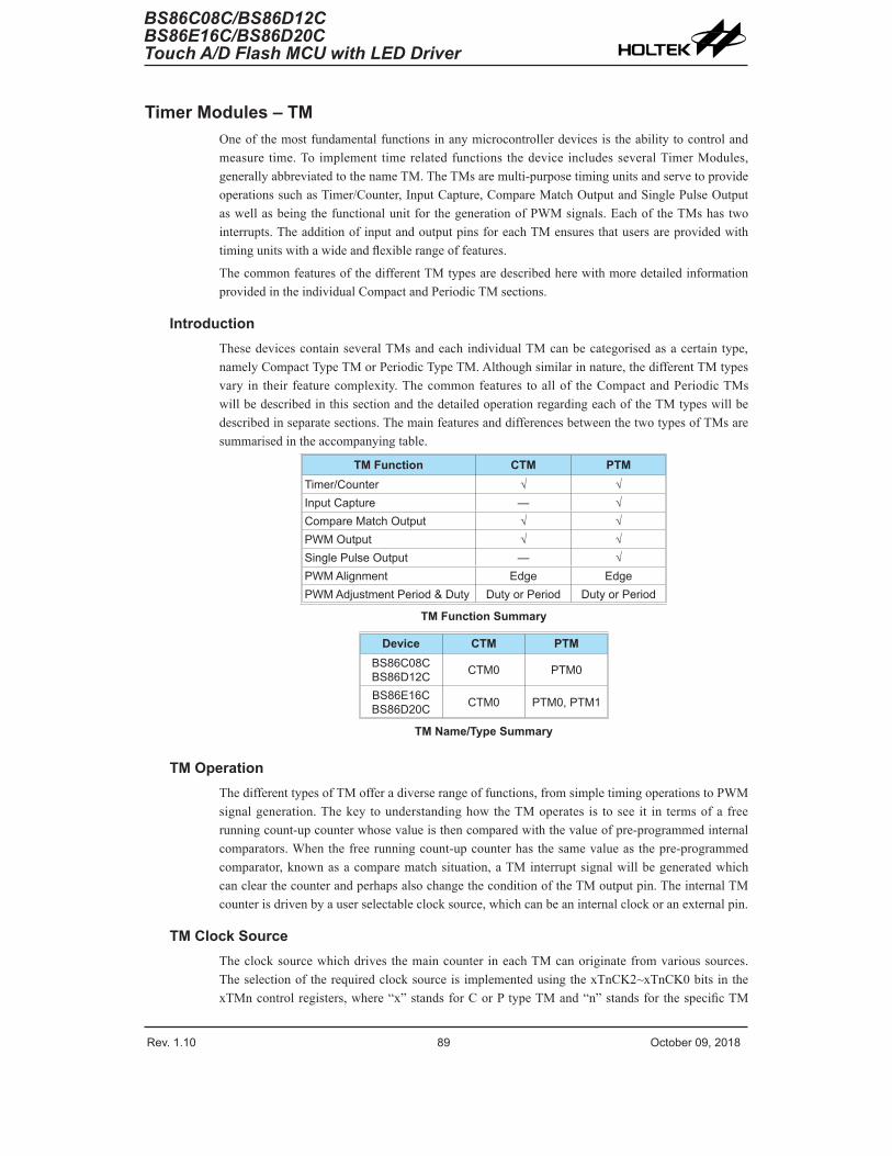
Rev. 1.10 88 October 09, 2018 Rev. 1.10 89 October 09, 2018
BS86C08C/BS86D12CBS86E16C/BS86D20C
Touch A/D Flash MCU with LED Driver
BS86C08C/BS86D12CBS86E16C/BS86D20CTouch A/D Flash MCU with LED Driver
Timer Modules – TMOne of the most fundamental functions in any microcontroller devices is the ability to control and measure time. To implement time related functions the device includes several Timer Modules, generally abbreviated to the name TM. The TMs are multi-purpose timing units and serve to provide operations such as Timer/Counter, Input Capture, Compare Match Output and Single Pulse Output as well as being the functional unit for the generation of PWM signals. Each of the TMs has two interrupts. The addition of input and output pins for each TM ensures that users are provided with timing units with a wide and flexible range of features.
The common features of the different TM types are described here with more detailed information provided in the individual Compact and Periodic TM sections.
IntroductionThese devices contain several TMs and each individual TM can be categorised as a certain type, namely Compact Type TM or Periodic Type TM. Although similar in nature, the different TM types vary in their feature complexity. The common features to all of the Compact and Periodic TMs will be described in this section and the detailed operation regarding each of the TM types will be described in separate sections. The main features and differences between the two types of TMs are summarised in the accompanying table.
TM Function CTM PTMTimer/Counter √ √Input Capture — √Compare Match Output √ √PWM Output √ √Single Pulse Output — √PWM Alignment Edge EdgePWM Adjustment Period & Duty Duty or Period Duty or Period
TM Function Summary
Device CTM PTMBS86C08CBS86D12C CTM0 PTM0
BS86E16CBS86D20C CTM0 PTM0, PTM1
TM Name/Type Summary
TM OperationThe different types of TM offer a diverse range of functions, from simple timing operations to PWM signal generation. The key to understanding how the TM operates is to see it in terms of a free running count-up counter whose value is then compared with the value of pre-programmed internal comparators. When the free running count-up counter has the same value as the pre-programmed comparator, known as a compare match situation, a TM interrupt signal will be generated which can clear the counter and perhaps also change the condition of the TM output pin. The internal TM counter is driven by a user selectable clock source, which can be an internal clock or an external pin.
TM Clock SourceThe clock source which drives the main counter in each TM can originate from various sources. The selection of the required clock source is implemented using the xTnCK2~xTnCK0 bits in the xTMn control registers, where “x” stands for C or P type TM and “n” stands for the specific TM

Rev. 1.10 90 October 09, 2018 Rev. 1.10 91 October 09, 2018
BS86C08C/BS86D12CBS86E16C/BS86D20C
Touch A/D Flash MCU with LED Driver
BS86C08C/BS86D12CBS86E16C/BS86D20CTouch A/D Flash MCU with LED Driver
serial number. The clock source can be a ratio of the system clock, fSYS, or the internal high clock, fH, the fSUB clock source or the external xTCKn pin. The xTCKn pin clock source is used to allow an external signal to drive the TM as an external clock source for event counting.
TM InterruptsThe Compact or Periodic type TM each has two internal interrupt, one for each of the internal comparator A or comparator P, which generate a TM interrupt when a compare match condition occurs. When a TM interrupt is generated, it can be used to clear the counter and also to change the state of the TM output pin.
TM External PinsEach of the TMs, irrespective of what type, has one input pin with the label xTCKn while the Periodic TMs have another input pin with the label PTPnI. The xTMn input pin, xTCKn, is essentially a clock source for the xTMn and is selected using the xTnCK2~xTnCK0 bits in the xTMnC0 register. This external TM input pin allows an external clock source to drive the internal TM. The xTCKn input pin can be chosen to have either a rising or falling active edge. The PTCKn pins are also used as the external trigger input pin in single pulse output mode for the PTMn.
The other PTMn input pin, PTPnI, is the capture input whose active edge can be a rising edge, a falling edge or both rising and falling edges and the active edge transition type is selected using the PTnIO1~PTnIO0 bits in the PTMnC1 register. There is another capture input, PTCKn, for PTMn capture input mode, which can be used as the external trigger input source except the PTPnI pin.
The TMs each have two output pins, xTPn and xTPnB. The xTPnB pin outputs the inverted signal of the xTPn. When the TM is in the Compare Match Output Mode, these pins can be controlled by the TM to switch to a high or low level or to toggle when a compare match situation occurs. The external xTPn and xTPnB output pins are also the pins where the xTMn generates the PWM output waveform. As the xTMn output pins are pin-shared with other functions, the TM output function must first be setup using the relevant registers. A signal bit in the register determines if its associated pin is to be used as an external TM output pin or if it is to have another function. The number of external pins for each TM type is different, the details are provided in the accompanying table.
DeviceCTM PTM
Input Output Input OutputBS86C08CBS86D12C CTCK0 CTP0, CTP0B PTCK0, PTP0I PTP0, PTP0B
BS86E16CBS86D20C CTCK0 CTP0, CTP0B PTCK0, PTP0I
PTCK1, PTP1IPTP0, PTP0BPTP1, PTP1B
TM External Pins
TM Input/Output Pin Control RegisterSelecting to have a TM input/output or whether to retain its other shared function is implemented using one register, with a single bit in the register corresponding to a TM input/output pin. Setting the bit high will setup the corresponding pin as a TM input/output, if reset to zero the pin will retain its original other function.
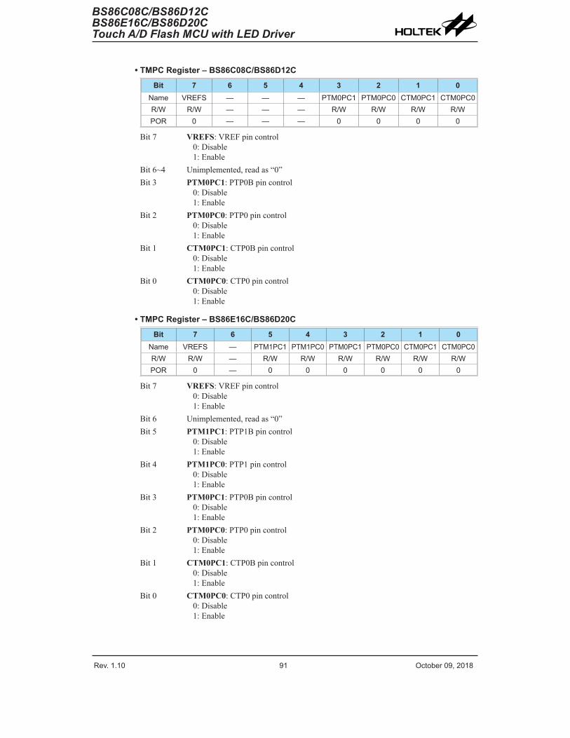
Rev. 1.10 90 October 09, 2018 Rev. 1.10 91 October 09, 2018
BS86C08C/BS86D12CBS86E16C/BS86D20C
Touch A/D Flash MCU with LED Driver
BS86C08C/BS86D12CBS86E16C/BS86D20CTouch A/D Flash MCU with LED Driver
• TMPC Register – BS86C08C/BS86D12C
Bit 7 6 5 4 3 2 1 0Name VREFS — — — PTM0PC1 PTM0PC0 CTM0PC1 CTM0PC0R/W R/W — — — R/W R/W R/W R/WPOR 0 — — — 0 0 0 0
Bit 7 VREFS: VREF pin control0: Disable1: Enable
Bit 6~4 Unimplemented, read as “0”Bit 3 PTM0PC1: PTP0B pin control
0: Disable1: Enable
Bit 2 PTM0PC0: PTP0 pin control0: Disable1: Enable
Bit 1 CTM0PC1: CTP0B pin control0: Disable1: Enable
Bit 0 CTM0PC0: CTP0 pin control0: Disable1: Enable
• TMPC Register – BS86E16C/BS86D20C
Bit 7 6 5 4 3 2 1 0Name VREFS — PTM1PC1 PTM1PC0 PTM0PC1 PTM0PC0 CTM0PC1 CTM0PC0R/W R/W — R/W R/W R/W R/W R/W R/WPOR 0 — 0 0 0 0 0 0
Bit 7 VREFS: VREF pin control0: Disable1: Enable
Bit 6 Unimplemented, read as “0”Bit 5 PTM1PC1: PTP1B pin control
0: Disable1: Enable
Bit 4 PTM1PC0: PTP1 pin control0: Disable1: Enable
Bit 3 PTM0PC1: PTP0B pin control0: Disable1: Enable
Bit 2 PTM0PC0: PTP0 pin control0: Disable1: Enable
Bit 1 CTM0PC1: CTP0B pin control0: Disable1: Enable
Bit 0 CTM0PC0: CTP0 pin control0: Disable1: Enable
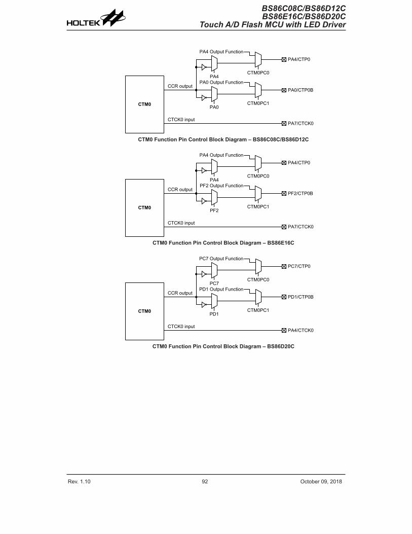
Rev. 1.10 92 October 09, 2018 Rev. 1.10 93 October 09, 2018
BS86C08C/BS86D12CBS86E16C/BS86D20C
Touch A/D Flash MCU with LED Driver
BS86C08C/BS86D12CBS86E16C/BS86D20CTouch A/D Flash MCU with LED Driver
CTM0
PA7/CTCK0
PA0/CTP0BCCR output
CTCK0 input
PA4
PA0
CTM0PC0
PA4 Output Function
CTM0PC1
PA0 Output Function
PA4/CTP0
CTM0 Function Pin Control Block Diagram – BS86C08C/BS86D12C
CTM0
PA7/CTCK0
PF2/CTP0BCCR output
CTCK0 input
PA4
PF2
CTM0PC0
PA4 Output Function
CTM0PC1
PF2 Output Function
PA4/CTP0
CTM0 Function Pin Control Block Diagram – BS86E16C
CTM0
PA4/CTCK0
PD1/CTP0BCCR output
CTCK0 input
PC7
PD1
CTM0PC0
PC7 Output Function
CTM0PC1
PD1 Output Function
PC7/CTP0
CTM0 Function Pin Control Block Diagram – BS86D20C

Rev. 1.10 92 October 09, 2018 Rev. 1.10 93 October 09, 2018
BS86C08C/BS86D12CBS86E16C/BS86D20C
Touch A/D Flash MCU with LED Driver
BS86C08C/BS86D12CBS86E16C/BS86D20CTouch A/D Flash MCU with LED Driver
PTM0
PA7/PTCK0
PA2/PTP0BCCR output
PTCK0 input
PD5
PA2
PTM0PC0
PD5 Output Function
PTM0PC1
PA2 Output Function
PD5/PTP0
PT0CAPTS
PTM0 Capture input PA4/PTP0I
PTM0 Function Pin Control Block Diagram – BS86C08C/BS86D12C
PTM0
PA7/PTCK0
PA2/PTP0BCCR output
PTCK0 input
PF3
PA2
PTM0PC0
PF3 Output Function
PTM0PC1
PA2 Output Function
PF3/PTP0
PT0CAPTS
PTM0 Capture input PA4/PTP0I
PTM0 Function Pin Control Block Diagram – BS86E16C
PTM0
PA0/PTCK0
PD0/PTP0BCCR output
PTCK0 input
PC6
PD0
PTM0PC0
PC6 Output Function
PTM0PC1
PD0 Output Function
PC6/PTP0
PT0CAPTS
PTM0 Capture input PA2/PTP0I
PTM0 Function Pin Control Block Diagram – BS86D20C

Rev. 1.10 94 October 09, 2018 Rev. 1.10 95 October 09, 2018
BS86C08C/BS86D12CBS86E16C/BS86D20C
Touch A/D Flash MCU with LED Driver
BS86C08C/BS86D12CBS86E16C/BS86D20CTouch A/D Flash MCU with LED Driver
PTM1
PE7/PTCK1
PE5/PTP1BCCR output
PTCK1 input
PE4
PE5
PTM1PC0
PE4 Output Function
PTM1PC1
PE5 Output Function
PE4/PTP1
PT1CAPTS
PTM1 Capture input PE6/PTP1I
PTM1 Function Pin Control Block Diagram – BS86E16C
PTM1
PB5/PTCK1
PD3/PTP1BCCR output
PTCK1 input
PB6
PD3
PTM1PC0
PB6 Output Function
PTM1PC1
PD3 Output Function
PB6/PTP1
PT1CAPTS
PTM1 Capture input PB7/PTP1I
PTM1 Function Pin Control Block Diagram – BS86D20C
Programming ConsiderationsThe TM Counter Registers and the Capture/Compare CCRA and CCRP registers, all have a low and high byte structure. The high bytes can be directly accessed, but as the low bytes can only be accessed via an internal 8-bit buffer, reading or writing to these register pairs must be carried out in a specific way. The important point to note is that data transfer to and from the 8-bit buffer and its related low byte only takes place when a write or read operation to its corresponding high byte is executed.
As the CCRA and CCRP registers are implemented in the way shown in the following diagram and accessing these register pairs is carried out in a specific way as described above, it is recommended to use the “MOV” instruction to access the CCRA and CCRP low byte registers, named xTMnAL and PTMnRPL, using the following access procedures. Accessing the CCRA or CCRP low byte registers without following these access procedures will result in unpredictable values.

Rev. 1.10 94 October 09, 2018 Rev. 1.10 95 October 09, 2018
BS86C08C/BS86D12CBS86E16C/BS86D20C
Touch A/D Flash MCU with LED Driver
BS86C08C/BS86D12CBS86E16C/BS86D20CTouch A/D Flash MCU with LED Driver
Data Bus
8-bit Buffer
xTMnDHxTMnDL
xTMnAHxTMnAL
xTMn Counter Register (Read only)
xTMn CCRA Register (Read/Write)
PTMnRPHPTMnRPL
PTMn CCRP Register (Read/Write)
The following steps show the read and write procedures:
• Writing Data to CCRA or CCRP ♦ Step 1. Write data to Low Byte xTMnAL or PTMnRPL
– Note that here data is only written to the 8-bit buffer. ♦ Step 2. Write data to High Byte xTMnAH or PTMnRPH
– Here data is written directly to the high byte registers and simultaneously data is latched from the 8-bit buffer to the Low Byte registers.
• Reading Data from the Counter Registers and CCRA or CCRP ♦ Step 1. Read data from the High Byte xTMnDH, xTMnAH or PTMnRPH
– Here data is read directly from the High Byte registers and simultaneously data is latched from the Low Byte register into the 8-bit buffer.
♦ Step 2. Read data from the Low Byte xTMnDL, xTMnAL or PTMnRPL – This step reads data from the 8-bit buffer.

Rev. 1.10 96 October 09, 2018 Rev. 1.10 97 October 09, 2018
BS86C08C/BS86D12CBS86E16C/BS86D20C
Touch A/D Flash MCU with LED Driver
BS86C08C/BS86D12CBS86E16C/BS86D20CTouch A/D Flash MCU with LED Driver
Compact Type TM – CTMThe Compact Type TM contains three operating modes, which are Compare Match Output, Timer/Event Counter and PWM Output modes. The Compact TM can also be controlled with an external input pin and can drive two external output pins.
Device CTM Core CTM Input Pin CTM Output PinBS86C08CBS86D12CBS86E16CBS86D20C
10-bit CTM (CTM0) CTCK0 CTP0, CTP0B
fSYS
fSYS/4
fH/64fH/16
fSUB
CTCKn
000001010011100101110111
CTnCK2~CTnCK0
10-bit Count-up Counter
3-bit Comparator P
CCRP
b7~b9
b0~b9
10-bit Comparator A
CTnONCTnPAU
Comparator A Match
Comparator P Match
Counter Clear 01
Output Control
Polarity Control
CTnOC
CTnM1, CTnM0CTnIO1, CTnIO0
CTMnAF Interrupt
CTMnPF Interrupt
CTnPOL
CCRA
CTnCCLRfSUB CTPnB
CTPn
Note: The CTPnB pin outputs the inverted signal of the CTPn. Compact Type TM Block Diagram (n=0)
Compact Type TM OperationThe size of Compact TM is 10-bit wide and its core is a 10-bit count-up counter which is driven by a user selectable internal or external clock source. There are also two internal comparators with the names, Comparator A and Comparator P. These comparators will compare the value in the counter with CCRP and CCRA registers. The CCRP comparator is 3-bit wide whose value is compared with the highest 3 bits in the counter while the CCRA is the 10 bits and therefore compares all counter bits.
The only way of changing the value of the 10-bit counter using the application program, is to clear the counter by changing the CTnON bit from low to high. The counter will also be cleared automatically by a counter overflow or a compare match with one of its associated comparators. When these conditions occur, a CTMn interrupt signal will also usually be generated. The Compact Type TM can operate in a number of different operational modes, can be driven by different clock sources including an input pin and can also control two output pins. All operating setup conditions are selected using relevant internal registers.
Compact Type TM Register DescriptionOverall operation of the Compact TM is controlled using a series of registers. A read only register pair exists to store the internal counter 10-bit value, while a read/write register pair exists to store the internal 10-bit CCRA value. The remaining two registers are control registers which setup the different operating and control modes as well as the CCRP bits.

Rev. 1.10 96 October 09, 2018 Rev. 1.10 97 October 09, 2018
BS86C08C/BS86D12CBS86E16C/BS86D20C
Touch A/D Flash MCU with LED Driver
BS86C08C/BS86D12CBS86E16C/BS86D20CTouch A/D Flash MCU with LED Driver
RegisterName
Bit
7 6 5 4 3 2 1 0CTMnC0 CTnPAU CTnCK2 CTnCK1 CTnCK0 CTnON CTnRP2 CTnRP1 CTnRP0CTMnC1 CTnM1 CTnM0 CTnIO1 CTnIO0 CTnOC CTnPOL CTnDPX CTnCCLRCTMnDL D7 D6 D5 D4 D3 D2 D1 D0CTMnDH — — — — — — D9 D8CTMnAL D7 D6 D5 D4 D3 D2 D1 D0CTMnAH — — — — — — D9 D8
10-bit Compact Type TM Register List (n=0)
• CTMnC0 Register
Bit 7 6 5 4 3 2 1 0Name CTnPAU CTnCK2 CTnCK1 CTnCK0 CTnON CTnRP2 CTnRP1 CTnRP0R/W R/W R/W R/W R/W R/W R/W R/W R/WPOR 0 0 0 0 0 0 0 0
Bit 7 CTnPAU: CTMn Counter Pause control0: Run1: Pause
The counter can be paused by setting this bit high. Clearing the bit to zero restores normal counter operation. When in a Pause condition the CTMn will remain powered up and continue to consume power. The counter will retain its residual value when this bit changes from low to high and resume counting from this value when the bit changes to a low value again.
Bit 6~4 CTnCK2~CTnCK0: Select CTMn Counter clock000: fSYS/4001: fSYS
010: fH/16011: fH/64100: fSUB
101: fSUB
110: CTCKn rising edge clock111: CTCKn falling edge clock
These three bits are used to select the clock source for the CTMn. The external pin clock source can be chosen to be active on the rising or falling edge. The clock source fSYS is the system clock, while fH and fSUB are other internal clocks, the details of which can be found in the oscillator section.
Bit 3 CTnON: CTMn Counter On/Off control0: Off1: On
This bit controls the overall on/off function of the CTMn. Setting the bit high enables the counter to run while clearing the bit disables the CTMn. Clearing this bit to zero will stop the counter from counting and turn off the CTMn which will reduce its power consumption. When the bit changes state from low to high the internal counter value will be reset to zero, however when the bit changes from high to low, the internal counter will retain its residual value until the bit returns high again. If the CTMn is in the Compare Match Output Mode or the PWM Output Mode then the CTMn output pin will be reset to its initial condition, as specified by the CTnOC bit, when the CTnON bit changes from low to high.

Rev. 1.10 98 October 09, 2018 Rev. 1.10 99 October 09, 2018
BS86C08C/BS86D12CBS86E16C/BS86D20C
Touch A/D Flash MCU with LED Driver
BS86C08C/BS86D12CBS86E16C/BS86D20CTouch A/D Flash MCU with LED Driver
Bit 2~0 CTnRP2~CTnRP0: CTMn CCRP 3-bit register, compared with the CTMn counter bit 9~bit 7Comparator P match period=
0: 1024 CTMn clocks1~7: (1~7)×128 CTMn clocks
These three bits are used to setup the value on the internal CCRP 3-bit register, which are then compared with the internal counter’s highest three bits. The result of this comparison can be selected to clear the internal counter if the CTnCCLR bit is set to zero. Setting the CTnCCLR bit to zero ensures that a compare match with the CCRP values will reset the internal counter. As the CCRP bits are only compared with the highest three counter bits, the compare values exist in 128 clock cycle multiples. Clearing all three bits to zero is in effect allowing the counter to overflow at its maximum value.
• CTMnC1 Register
Bit 7 6 5 4 3 2 1 0Name CTnM1 CTnM0 CTnIO1 CTnIO0 CTnOC CTnPOL CTnDPX CTnCCLRR/W R/W R/W R/W R/W R/W R/W R/W R/WPOR 0 0 0 0 0 0 0 0
Bit 7~6 CTnM1~CTnM0: Select CTMn Operating Mode00: Compare Match Output Mode01: Undefined10: PWM Output Mode11: Timer/Counter Mode
These bits setup the required operating mode for the CTMn. To ensure reliable operation the CTMn should be switched off before any changes are made to the CTnM1 and CTnM0 bits. In the Timer/Counter Mode, the CTMn output pin control will be disabled.
Bit 5~4 CTnIO1~CTnIO0: Select CTMn external pin CTPn functionCompare Match Output Mode
00: No change01: Output low10: Output high11: Toggle output
PWM Output Mode00: PWM output inactive state01: PWM output active state10: PWM output11: Undefined
Timer/Counter ModeUnused
These two bits are used to determine how the CTMn external pin changes state when a certain condition is reached. The function that these bits select depends upon in which mode the CTMn is running.In the Compare Match Output Mode, the CTnIO1 and CTnIO0 bits determine how the CTMn output pin changes state when a compare match occurs from the Comparator A. The CTMn output pin can be setup to switch high, switch low or to toggle its present state when a compare match occurs from the Comparator A. When the bits are both zero, then no change will take place on the output. The initial value of the CTMn output pin should be setup using the CTnOC bit in the CTMnC1 register. Note that the output level requested by the CTnIO1 and CTnIO0 bits must be different from the initial value setup using the CTnOC bit otherwise no change will occur on the CTMn output pin when a compare match occurs. After the CTMn output pin changes state, it can be reset to its initial level by changing the level of the CTnON bit from low to high.

Rev. 1.10 98 October 09, 2018 Rev. 1.10 99 October 09, 2018
BS86C08C/BS86D12CBS86E16C/BS86D20C
Touch A/D Flash MCU with LED Driver
BS86C08C/BS86D12CBS86E16C/BS86D20CTouch A/D Flash MCU with LED Driver
In the PWM Output Mode, the CTnIO1 and CTnIO0 bits determine how the CTMn output pin changes state when a certain compare match condition occurs. The PWM output function is modified by changing these two bits. It is necessary to only change the values of the CTnIO1 and CTnIO0 bits only after the CTMn has been switched off. Unpredictable PWM outputs will occur if the CTnIO1 and CTnIO0 bits are changed when the CTMn is running.
Bit 3 CTnOC: CTMn CTPn Output controlCompare Match Output Mode
0: Initial low1: Initial high
PWM Output Mode/Single Pulse Output Mode0: Active low1: Active high
This is the output control bit for the CTMn output pin. Its operation depends upon whether CTMn is being used in the Compare Match Output Mode or in the PWM Output Mode. It has no effect if the CTMn is in the Timer/Counter Mode. In the Compare Match Output Mode it determines the logic level of the CTMn output pin before a compare match occurs. In the PWM Output Mode it determines if the PWM signal is active high or active low.
Bit 2 CTnPOL: CTMn CTPn Output polarity control0: Non-invert1: Invert
This bit controls the polarity of the CTPn output pin. When the bit is set high the CTMn output pin will be inverted and not inverted when the bit is zero. It has no effect if the CTMn is in the Timer/Counter Mode.
Bit 1 CTnDPX: CTMn PWM duty/period control0: CCRP – period; CCRA – duty1: CCRP – duty; CCRA – period
This bit determines which of the CCRA and CCRP registers are used for period and duty control of the PWM waveform.
Bit 0 CTCCLR: CTMn Counter Clear condition selection0: Comparator P match1: Comparator A match
This bit is used to select the method which clears the counter. Remember that the CTMn contains two comparators, Comparator A and Comparator P, either of which can be selected to clear the internal counter. With the CTnCCLR bit set high, the counter will be cleared when a compare match occurs from the Comparator A. When the bit is low, the counter will be cleared when a compare match occurs from the Comparator P or with a counter overflow. A counter overflow clearing method can only be implemented if the CCRP bits are all cleared to zero. The CTnCCLR bit is not used in the PWM Output mode.

Rev. 1.10 100 October 09, 2018 Rev. 1.10 101 October 09, 2018
BS86C08C/BS86D12CBS86E16C/BS86D20C
Touch A/D Flash MCU with LED Driver
BS86C08C/BS86D12CBS86E16C/BS86D20CTouch A/D Flash MCU with LED Driver
• CTMnDL Register
Bit 7 6 5 4 3 2 1 0Name D7 D6 D5 D4 D3 D2 D1 D0R/W R R R R R R R RPOR 0 0 0 0 0 0 0 0
Bit 7~0 D7~D0: CTMn Counter Low Byte Register bit 7~bit 0CTMn 10-bit Counter bit 7~bit 0
• CTMnDH Register
Bit 7 6 5 4 3 2 1 0Name — — — — — — D9 D8R/W — — — — — — R RPOR — — — — — — 0 0
Bit 7~2 Unimplemented, read as “0”Bit 1~0 D9~D8: CTMn Counter High Byte Register bit 1~bit 0
CTMn 10-bit Counter bit 9~bit 8
• CTMnAL Register
Bit 7 6 5 4 3 2 1 0Name D7 D6 D5 D4 D3 D2 D1 D0R/W R/W R/W R/W R/W R/W R/W R/W R/WPOR 0 0 0 0 0 0 0 0
Bit 7~0 D7~D0: CTMn CCRA Low Byte Register bit 7~bit 0CTMn 10-bit CCRA bit 7~bit 0
• CTMnAH Register
Bit 7 6 5 4 3 2 1 0Name — — — — — — D9 D8R/W — — — — — — R/W R/WPOR — — — — — — 0 0
Bit 7~2 Unimplemented, read as “0”Bit 1~0 D9~D8: CTMn CCRA High Byte Register bit 7~bit 0
CTMn 10-bit CCRA bit 9~bit 8

Rev. 1.10 100 October 09, 2018 Rev. 1.10 101 October 09, 2018
BS86C08C/BS86D12CBS86E16C/BS86D20C
Touch A/D Flash MCU with LED Driver
BS86C08C/BS86D12CBS86E16C/BS86D20CTouch A/D Flash MCU with LED Driver
Compact Type TM Operation ModesThe Compact Type TM can operate in one of three operating modes, Compare Match Output Mode, PWM Output Mode or Timer/Counter Mode. The operating mode is selected using the CTnM1 and CTnM0 bits in the CTMnC1 register.
Compare Match Output ModeTo select this mode, bits CTnM1 and CTnM0 in the CTMnC1 register, should be set to 00 respectively. In this mode once the counter is enabled and running it can be cleared by three methods. These are a counter overflow, a compare match from Comparator A and a compare match from Comparator P. When the CTnCCLR bit is low, there are two ways in which the counter can be cleared. One is when a compare match from Comparator P, the other is when the CCRP bits are all zero which allows the counter to overflow. Here both CTMnAF and CTMnPF interrupt request flags for Comparator A and Comparator P respectively, will both be generated.
If the CTnCCLR bit in the CTMnC1 register is high then the counter will be cleared when a compare match occurs from Comparator A. However, here only the CTMnAF interrupt request flag will be generated even if the value of the CCRP bits is less than that of the CCRA registers. Therefore when CTnCCLR is high no CTMnPF interrupt request flag will be generated. If the CCRA bits are all zero, the counter will overflow when it reaches its maximum 10-bit, 3FF Hex, value. However, here the CTMnAF interrupt request flag will not be generated.
As the name of the mode suggests, after a comparison is made, the CTMn output pin, will change state. The CTMn output pin condition however only changes state when a CTMnAF interrupt request flag is generated after a compare match occurs from Comparator A. The CTMnPF interrupt request flag, generated from a compare match occurs from Comparator P, will have no effect on the CTMn output pin. The way in which the CTMn output pin changes state are determined by the condition of the CTnIO1 and CTnIO0 bits in the CTMnC1 register. The CTMn output pin can be selected using the CTnIO1 and CTnIO0 bits to go high, to go low or to toggle from its present condition when a compare match occurs from Comparator A. The initial condition of the CTMn output pin, which is setup after the CTnON bit changes from low to high, is setup using the CTnOC bit. Note that if the CTnIO1 and CTnIO0 bits are zero then no pin change will take place.
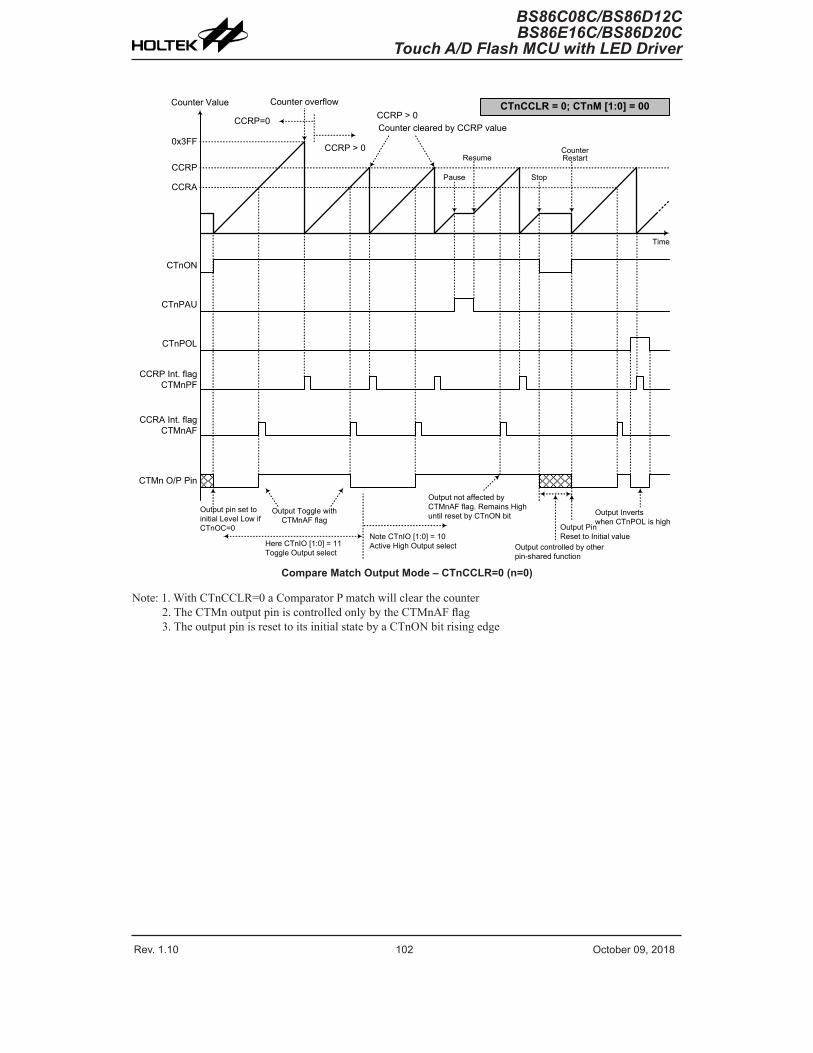
Rev. 1.10 102 October 09, 2018 Rev. 1.10 103 October 09, 2018
BS86C08C/BS86D12CBS86E16C/BS86D20C
Touch A/D Flash MCU with LED Driver
BS86C08C/BS86D12CBS86E16C/BS86D20CTouch A/D Flash MCU with LED Driver
Counter Value
0x3FF
CCRP
CCRA
CTnON
CTnPAU
CTnPOL
CCRP Int. flag CTMnPF
CCRA Int. flag CTMnAF
CTMn O/P Pin
Time
CCRP=0
CCRP > 0
Counter overflowCCRP > 0Counter cleared by CCRP value
Pause
Resume
Stop
Counter Restart
CTnCCLR = 0; CTnM [1:0] = 00
Output pin set to initial Level Low if CTnOC=0
Output Toggle with CTMnAF flag
Note CTnIO [1:0] = 10 Active High Output selectHere CTnIO [1:0] = 11
Toggle Output select
Output not affected by CTMnAF flag. Remains High until reset by CTnON bit
Output PinReset to Initial value
Output controlled by other pin-shared function
Output Invertswhen CTnPOL is high
Compare Match Output Mode – CTnCCLR=0 (n=0)
Note: 1. With CTnCCLR=0 a Comparator P match will clear the counter2. The CTMn output pin is controlled only by the CTMnAF flag3. The output pin is reset to its initial state by a CTnON bit rising edge

Rev. 1.10 102 October 09, 2018 Rev. 1.10 103 October 09, 2018
BS86C08C/BS86D12CBS86E16C/BS86D20C
Touch A/D Flash MCU with LED Driver
BS86C08C/BS86D12CBS86E16C/BS86D20CTouch A/D Flash MCU with LED Driver
Counter Value
0x3FF
CCRP
CCRA
CTnON
CTnPAU
CTnPOL
CTMn O/P Pin
Time
CCRA=0
CCRA = 0Counter overflowCCRA > 0 Counter cleared by CCRA value
Pause
Resume
Stop Counter Restart
Output pin set to initial Level Low if CTnOC=0
Output Toggle with CTMnAF flag
Note CTnIO [1:0] = 10 Active High Output selectHere CTnIO [1:0] = 11
Toggle Output select
Output not affected by CTMnAF flag. Remains High until reset by CTnON bit
Output PinReset to Initial value
Output controlled by other pin-shared function
Output Invertswhen CTnPOL is high
CTMnPF not generated
No CTMnAF flag generated on CCRA overflow
Output does not change
CTnCCLR = 1; CTnM [1:0] = 00
CCRA Int. flag CTMnAF
CCRP Int. flag CTMnPF
Compare Match Output Mode – CTnCCLR=1 (n=0)
Note: 1. With CTnCCLR=1 a Comparator A match will clear the counter2. The CTMn output pin is controlled only by the CTMnAF flag3. The output pin is reset to its initial state by a CTnON bit rising edge4. A CTMnPF flag is not generated when CTnCCLR=1
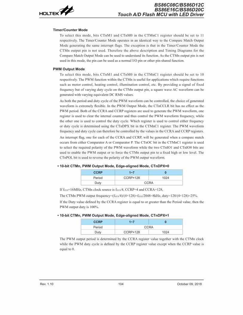
Rev. 1.10 104 October 09, 2018 Rev. 1.10 105 October 09, 2018
BS86C08C/BS86D12CBS86E16C/BS86D20C
Touch A/D Flash MCU with LED Driver
BS86C08C/BS86D12CBS86E16C/BS86D20CTouch A/D Flash MCU with LED Driver
Timer/Counter ModeTo select this mode, bits CTnM1 and CTnM0 in the CTMnC1 register should be set to 11 respectively. The Timer/Counter Mode operates in an identical way to the Compare Match Output Mode generating the same interrupt flags. The exception is that in the Timer/Counter Mode the CTMn output pin is not used. Therefore the above description and Timing Diagrams for the Compare Match Output Mode can be used to understand its function. As the CTMn output pin is not used in this mode, the pin can be used as a normal I/O pin or other pin-shared function.
PWM Output ModeTo select this mode, bits CTnM1 and CTnM0 in the CTMnC1 register should be set to 10 respectively. The PWM function within the CTMn is useful for applications which require functions such as motor control, heating control, illumination control, etc. By providing a signal of fixed frequency but of varying duty cycle on the CTMn output pin, a square wave AC waveform can be generated with varying equivalent DC RMS values.
As both the period and duty cycle of the PWM waveform can be controlled, the choice of generated waveform is extremely flexible. In the PWM Output Mode, the CTnCCLR bit has no effect as the PWM period. Both of the CCRA and CCRP registers are used to generate the PWM waveform, one register is used to clear the internal counter and thus control the PWM waveform frequency, while the other one is used to control the duty cycle. Which register is used to control either frequency or duty cycle is determined using the CTnDPX bit in the CTMnC1 register. The PWM waveform frequency and duty cycle can therefore be controlled by the values in the CCRA and CCRP registers.
An interrupt flag, one for each of the CCRA and CCRP, will be generated when a compare match occurs from either Comparator A or Comparator P. The CTnOC bit in the CTMnC1 register is used to select the required polarity of the PWM waveform while the two CTnIO1 and CTnIO0 bits are used to enable the PWM output or to force the CTMn output pin to a fixed high or low level. The CTnPOL bit is used to reverse the polarity of the PWM output waveform.
• 10-bit CTMn, PWM Output Mode, Edge-aligned Mode, CTnDPX=0
CCRP 1~7 0Period CCRP×128 1024Duty CCRA
If fSYS=16MHz, CTMn clock source is fSYS/4, CCRP=4 and CCRA=128,
The CTMn PWM output frequency=(fSYS/4)/(4×128)=fSYS/2048=8kHz, duty=128/(4×128)=25%.
If the Duty value defined by the CCRA register is equal to or greater than the Period value, then the PWM output duty is 100%.
• 10-bit CTMn, PWM Output Mode, Edge-aligned Mode, CTnDPX=1
CCRP 1~7 0Period CCRADuty CCRP×128 1024
The PWM output period is determined by the CCRA register value together with the CTMn clock while the PWM duty cycle is defined by the CCRP register value except when the CCRP value is equal to 0.

Rev. 1.10 104 October 09, 2018 Rev. 1.10 105 October 09, 2018
BS86C08C/BS86D12CBS86E16C/BS86D20C
Touch A/D Flash MCU with LED Driver
BS86C08C/BS86D12CBS86E16C/BS86D20CTouch A/D Flash MCU with LED Driver
Counter Value
CCRP
CCRA
CTnON
CTnPAU
CTnPOL
CTMn O/P Pin (CTnOC=1)
Time
Counter cleared by CCRP
Pause Resume Counter Stop if CTnON bit low
Counter Reset when CTnON returns high
PWM Duty Cycle set by CCRA
PWM resumes operationOutput controlled by other
pin-shared function Output Invertswhen CTnPOL = 1PWM Period set by CCRP
CTMn O/P Pin (CTnOC=0)
CCRA Int. flag CTMnAF
CCRP Int. flag CTMnPF
CTnDPX = 0; CTnM [1:0] = 10
PWM Output Mode – CTnDXP=0 (n=0)
Note: 1. Here CTnDPX=0 – Counter cleared by CCRP2. A counter clear sets the PWM Period3. The internal PWM function continues running even when CTnIO[1:0]=00 or 014. The CTnCCLR bit has no influence on PWM operation
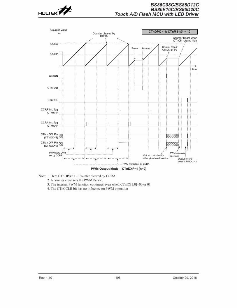
Rev. 1.10 106 October 09, 2018 Rev. 1.10 107 October 09, 2018
BS86C08C/BS86D12CBS86E16C/BS86D20C
Touch A/D Flash MCU with LED Driver
BS86C08C/BS86D12CBS86E16C/BS86D20CTouch A/D Flash MCU with LED Driver
Counter Value
CCRP
CCRA
CTnON
CTnPAU
CTnPOL
CCRP Int. flag CTMnPF
CCRA Int. flag CTMnAF
CTMn O/P Pin (CTnOC=1)
Time
Counter cleared by CCRA
Pause Resume Counter Stop if CTnON bit low
Counter Reset when CTnON returns high
PWM Duty Cycle set by CCRP
PWM resumes operationOutput controlled by
other pin-shared function Output Invertswhen CTnPOL = 1
PWM Period set by CCRA
CTMn O/P Pin (CTnOC=0)
CTnDPX = 1; CTnM [1:0] = 10
PWM Output Mode – CTnDXP=1 (n=0)
Note: 1. Here CTnDPX=1 – Counter cleared by CCRA2. A counter clear sets the PWM Period3. The internal PWM function continues even when CTnIO[1:0]=00 or 014. The CTnCCLR bit has no influence on PWM operation

Rev. 1.10 106 October 09, 2018 Rev. 1.10 107 October 09, 2018
BS86C08C/BS86D12CBS86E16C/BS86D20C
Touch A/D Flash MCU with LED Driver
BS86C08C/BS86D12CBS86E16C/BS86D20CTouch A/D Flash MCU with LED Driver
Periodic Type TM – PTMThe Periodic Type TM contains five operating modes, which are Compare Match Output, Timer/Event Counter, Capture Input, Single Pulse Output and PWM Output modes. The Periodic TM can also be controlled with two external input pins and can drive two external output pins.
Device PTM Core PTM Input Pin PTM Output PinBS86C08CBS86D12C 10-bit PTM (PTM0) PTCK0, PTP0I PTP0, PTP0B
BS86E16CBS86D20C 10-bit PTM (PTM0, PTM1) PTCK0, PTP0I
PTCK1, PTP1IPTP0, PTP0BPTP1, PTP1B
fSYS
fSYS/4
fH/64fH/16
fSUB
PTCKn
000001010011100101110111
PTnCK2~PTnCK0
10-bit Count-up Counter
10-bit Comparator P
CCRP
b0~b9
b0~b9
10-bit Comparator A
PTnONPTnPAU
Comparator A Match
Comparator P Match
Counter Clear 01
Output Control
Polarity Control
PTPnB
PTOC
PTnM1, PTnM0PTnIO1, PTnIO0
PTMnAF Interrupt
PTMnPF Interrupt
PTnPOL
CCRA
PTnCCLR
Edge Detector
PTPnI
PTnIO1, PTnIO0
10
PTnCAPTS
PTPn
fSUB
Note: The PTPnB pin outputs the inverted signal of the PTPn. Periodic Type TM Block Diagram (n=0~1)
Periodic TM OperationThe size of Periodic TM is 10-bit wide and its core is a 10-bit count-up counter which is driven by a user selectable internal or external clock source. There are also two internal comparators with the names, Comparator A and Comparator P. These comparators will compare the value in the counter with CCRP and CCRA registers. The CCRP and CCRA comparators are 10-bit wide whose value is respectively compared with all counter bits.
The only way of changing the value of the 10-bit counter using the application program is to clear the counter by changing the PTnON bit from low to high. The counter will also be cleared automatically by a counter overflow or a compare match with one of its associated comparators. When these conditions occur, a PTMn interrupt signal will also usually be generated. The Periodic Type TM can operate in a number of different operational modes, can be driven by different clock sources including an input pin and can also control the output pins. All operating setup conditions are selected using relevant internal registers.
Periodic Type TM Register DescriptionOverall operation of the Periodic TM is controlled using a series of registers. A read only register pair exists to store the internal counter 10-bit value, while two read/write register pairs exist to store the internal 10-bit CCRA and CCRP value. The remaining two registers are control registers which setup the different operating and control modes.
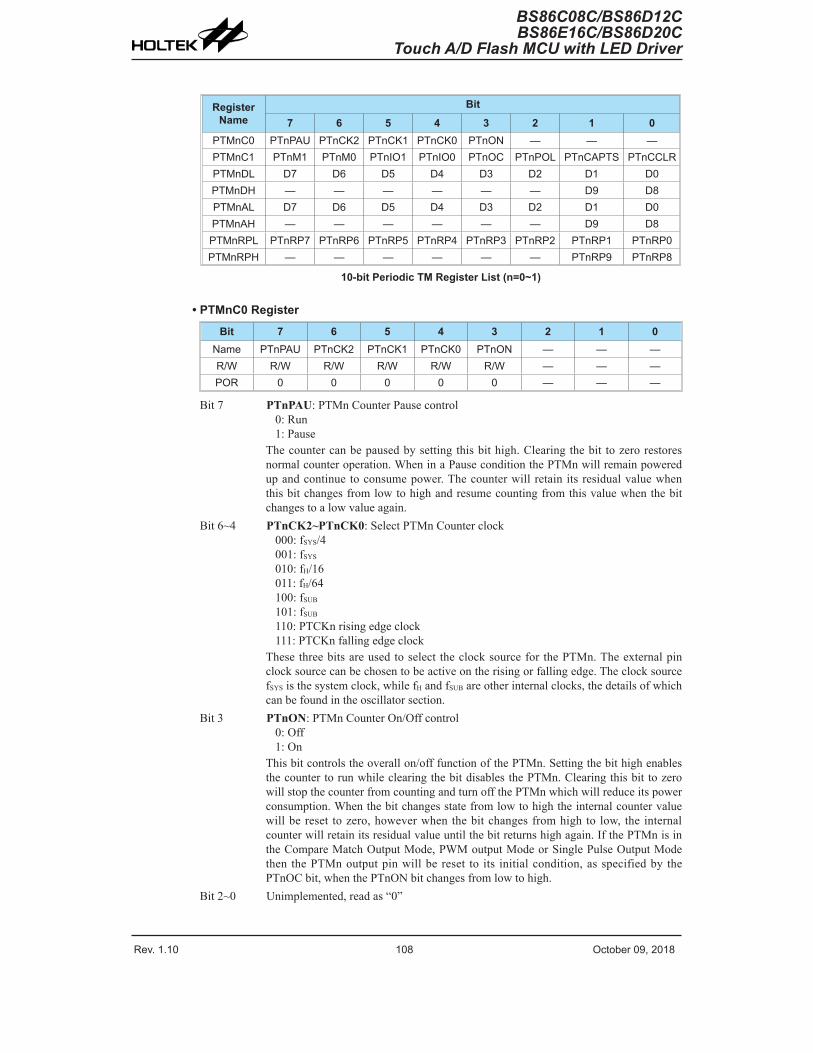
Rev. 1.10 108 October 09, 2018 Rev. 1.10 109 October 09, 2018
BS86C08C/BS86D12CBS86E16C/BS86D20C
Touch A/D Flash MCU with LED Driver
BS86C08C/BS86D12CBS86E16C/BS86D20CTouch A/D Flash MCU with LED Driver
RegisterName
Bit
7 6 5 4 3 2 1 0PTMnC0 PTnPAU PTnCK2 PTnCK1 PTnCK0 PTnON — — —PTMnC1 PTnM1 PTnM0 PTnIO1 PTnIO0 PTnOC PTnPOL PTnCAPTS PTnCCLRPTMnDL D7 D6 D5 D4 D3 D2 D1 D0PTMnDH — — — — — — D9 D8PTMnAL D7 D6 D5 D4 D3 D2 D1 D0PTMnAH — — — — — — D9 D8PTMnRPL PTnRP7 PTnRP6 PTnRP5 PTnRP4 PTnRP3 PTnRP2 PTnRP1 PTnRP0PTMnRPH — — — — — — PTnRP9 PTnRP8
10-bit Periodic TM Register List (n=0~1)
• PTMnC0 Register
Bit 7 6 5 4 3 2 1 0Name PTnPAU PTnCK2 PTnCK1 PTnCK0 PTnON — — —R/W R/W R/W R/W R/W R/W — — —POR 0 0 0 0 0 — — —
Bit 7 PTnPAU: PTMn Counter Pause control0: Run1: Pause
The counter can be paused by setting this bit high. Clearing the bit to zero restores normal counter operation. When in a Pause condition the PTMn will remain powered up and continue to consume power. The counter will retain its residual value when this bit changes from low to high and resume counting from this value when the bit changes to a low value again.
Bit 6~4 PTnCK2~PTnCK0: Select PTMn Counter clock000: fSYS/4001: fSYS
010: fH/16011: fH/64100: fSUB
101: fSUB
110: PTCKn rising edge clock111: PTCKn falling edge clock
These three bits are used to select the clock source for the PTMn. The external pin clock source can be chosen to be active on the rising or falling edge. The clock source fSYS is the system clock, while fH and fSUB are other internal clocks, the details of which can be found in the oscillator section.
Bit 3 PTnON: PTMn Counter On/Off control0: Off1: On
This bit controls the overall on/off function of the PTMn. Setting the bit high enables the counter to run while clearing the bit disables the PTMn. Clearing this bit to zero will stop the counter from counting and turn off the PTMn which will reduce its power consumption. When the bit changes state from low to high the internal counter value will be reset to zero, however when the bit changes from high to low, the internal counter will retain its residual value until the bit returns high again. If the PTMn is in the Compare Match Output Mode, PWM output Mode or Single Pulse Output Mode then the PTMn output pin will be reset to its initial condition, as specified by the PTnOC bit, when the PTnON bit changes from low to high.
Bit 2~0 Unimplemented, read as “0”
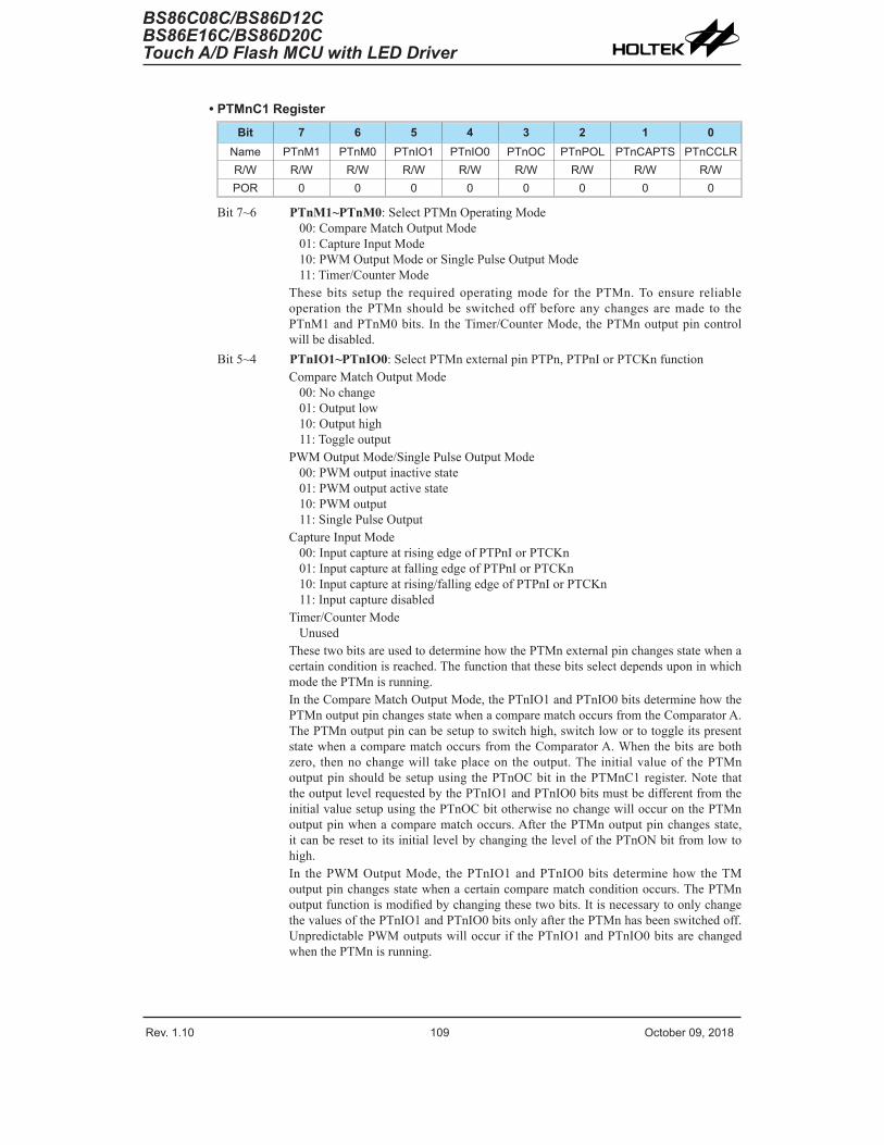
Rev. 1.10 108 October 09, 2018 Rev. 1.10 109 October 09, 2018
BS86C08C/BS86D12CBS86E16C/BS86D20C
Touch A/D Flash MCU with LED Driver
BS86C08C/BS86D12CBS86E16C/BS86D20CTouch A/D Flash MCU with LED Driver
• PTMnC1 Register
Bit 7 6 5 4 3 2 1 0Name PTnM1 PTnM0 PTnIO1 PTnIO0 PTnOC PTnPOL PTnCAPTS PTnCCLRR/W R/W R/W R/W R/W R/W R/W R/W R/WPOR 0 0 0 0 0 0 0 0
Bit 7~6 PTnM1~PTnM0: Select PTMn Operating Mode00: Compare Match Output Mode01: Capture Input Mode10: PWM Output Mode or Single Pulse Output Mode11: Timer/Counter Mode
These bits setup the required operating mode for the PTMn. To ensure reliable operation the PTMn should be switched off before any changes are made to the PTnM1 and PTnM0 bits. In the Timer/Counter Mode, the PTMn output pin control will be disabled.
Bit 5~4 PTnIO1~PTnIO0: Select PTMn external pin PTPn, PTPnI or PTCKn functionCompare Match Output Mode
00: No change01: Output low10: Output high11: Toggle output
PWM Output Mode/Single Pulse Output Mode00: PWM output inactive state01: PWM output active state10: PWM output11: Single Pulse Output
Capture Input Mode00: Input capture at rising edge of PTPnI or PTCKn01: Input capture at falling edge of PTPnI or PTCKn10: Input capture at rising/falling edge of PTPnI or PTCKn11: Input capture disabled
Timer/Counter ModeUnused
These two bits are used to determine how the PTMn external pin changes state when a certain condition is reached. The function that these bits select depends upon in which mode the PTMn is running.In the Compare Match Output Mode, the PTnIO1 and PTnIO0 bits determine how the PTMn output pin changes state when a compare match occurs from the Comparator A. The PTMn output pin can be setup to switch high, switch low or to toggle its present state when a compare match occurs from the Comparator A. When the bits are both zero, then no change will take place on the output. The initial value of the PTMn output pin should be setup using the PTnOC bit in the PTMnC1 register. Note that the output level requested by the PTnIO1 and PTnIO0 bits must be different from the initial value setup using the PTnOC bit otherwise no change will occur on the PTMn output pin when a compare match occurs. After the PTMn output pin changes state, it can be reset to its initial level by changing the level of the PTnON bit from low to high.In the PWM Output Mode, the PTnIO1 and PTnIO0 bits determine how the TM output pin changes state when a certain compare match condition occurs. The PTMn output function is modified by changing these two bits. It is necessary to only change the values of the PTnIO1 and PTnIO0 bits only after the PTMn has been switched off. Unpredictable PWM outputs will occur if the PTnIO1 and PTnIO0 bits are changed when the PTMn is running.

Rev. 1.10 110 October 09, 2018 Rev. 1.10 111 October 09, 2018
BS86C08C/BS86D12CBS86E16C/BS86D20C
Touch A/D Flash MCU with LED Driver
BS86C08C/BS86D12CBS86E16C/BS86D20CTouch A/D Flash MCU with LED Driver
Bit 3 PTnOC: PTMn PTPn Output controlCompare Match Output Mode
0: Initial low1: Initial high
PWM Output Mode/Single Pulse Output Mode0: Active low1: Active high
This is the output control bit for the PTMn output pin. Its operation depends upon whether PTMn is being used in the Compare Match Output Mode or in the PWM Output Mode/Single Pulse Output Mode. It has no effect if the PTMn is in the Timer/Counter Mode. In the Compare Match Output Mode it determines the logic level of the PTMn output pin before a compare match occurs. In the PWM Output Mode it determines if the PWM signal is active high or active low. In the Single Pulse Output Mode it determines the logic level of the PTMn output pin when the PTnON bit changes from low to high.
Bit 2 PTnPOL: PTMn PTPn Output polarity control0: Non-invert1: Invert
This bit controls the polarity of the PTPn output pin. When the bit is set high the PTMn output pin will be inverted and not inverted when the bit is zero. It has no effect if the PTMn is in the Timer/Counter Mode.
Bit 1 PTnCAPTS: PTMn Capture Trigger Source selection0: From PTPnI pin1: From PTCKn pin
Bit 0 PTnCCLR: PTMn Counter Clear condition selection0: Comparator P match1: Comparator A match
This bit is used to select the method which clears the counter. Remember that the Periodic TM contains two comparators, Comparator A and Comparator P, either of which can be selected to clear the internal counter. With the PTnCCLR bit set high, the counter will be cleared when a compare match occurs from the Comparator A. When the bit is low, the counter will be cleared when a compare match occurs from the Comparator P or with a counter overflow. A counter overflow clearing method can only be implemented if the CCRP bits are all cleared to zero. The PTnCCLR bit is not used in the PWM Output, Single Pulse Output or Capture Input Mode.
• PTMnDL Register
Bit 7 6 5 4 3 2 1 0Name D7 D6 D5 D4 D3 D2 D1 D0R/W R R R R R R R RPOR 0 0 0 0 0 0 0 0
Bit 7~0 D7~D0: PTMn Counter Low Byte Register bit 7~bit 0PTMn 10-bit Counter bit 7~bit 0
• PTMnDH Register
Bit 7 6 5 4 3 2 1 0Name — — — — — — D9 D8R/W — — — — — — R RPOR — — — — — — 0 0
Bit 7~2 Unimplemented, read as “0”Bit 1~0 D9~D8: PTMn Counter High Byte Register bit 1~bit 0
PTMn 10-bit Counter bit 9~bit 8

Rev. 1.10 110 October 09, 2018 Rev. 1.10 111 October 09, 2018
BS86C08C/BS86D12CBS86E16C/BS86D20C
Touch A/D Flash MCU with LED Driver
BS86C08C/BS86D12CBS86E16C/BS86D20CTouch A/D Flash MCU with LED Driver
• PTMnAL Register
Bit 7 6 5 4 3 2 1 0Name D7 D6 D5 D4 D3 D2 D1 D0R/W R/W R/W R/W R/W R/W R/W R/W R/WPOR 0 0 0 0 0 0 0 0
Bit 7~0 D7~D0: PTMn CCRA Low Byte Register bit 7~bit 0PTMn 10-bit CCRA bit 7~bit 0
• PTMnAH Register
Bit 7 6 5 4 3 2 1 0Name — — — — — — D9 D8R/W — — — — — — R/W R/WPOR — — — — — — 0 0
Bit 7~2 Unimplemented, read as “0”Bit 1~0 D9~D8: PTMn CCRA High Byte Register bit 1~bit 0
PTMn 10-bit CCRA bit 9~bit 8
• PTMnRPL Register
Bit 7 6 5 4 3 2 1 0Name PTnRP7 PTnRP6 PTnRP5 PTnRP4 PTnRP3 PTnRP2 PTnRP1 PTnRP0R/W R/W R/W R/W R/W R/W R/W R/W R/WPOR 0 0 0 0 0 0 0 0
Bit 7~0 PTnRP7~PTnRP0: PTMn CCRP Low Byte Register bit 7~bit 0PTMn 10-bit CCRP bit 7~bit 0
• PTMnRPH Register
Bit 7 6 5 4 3 2 1 0Name — — — — — — PTnRP9 PTnRP8R/W — — — — — — R/W R/WPOR — — — — — — 0 0
Bit 7~2 Unimplemented, read as “0”Bit 1~0 PTnRP9~PTnRP8: PTMn CCRP High Byte Register bit 1~bit 0
PTMn 10-bit CCRP bit 9~bit 8

Rev. 1.10 112 October 09, 2018 Rev. 1.10 113 October 09, 2018
BS86C08C/BS86D12CBS86E16C/BS86D20C
Touch A/D Flash MCU with LED Driver
BS86C08C/BS86D12CBS86E16C/BS86D20CTouch A/D Flash MCU with LED Driver
Periodic Type TM Operation ModesThe Periodic Type TM can operate in one of five operating modes, Compare Match Output Mode, PWM Output Mode, Single Pulse Output Mode, Capture Input Mode or Timer/Counter Mode. The operating mode is selected using the PTnM1 and PTnM0 bits in the PTMnC1 register.
Compare Match Output ModeTo select this mode, bits PTnM1 and PTnM0 in the PTMnC1 register, should be set to 00 respectively. In this mode once the counter is enabled and running it can be cleared by three methods. These are a counter overflow, a compare match from Comparator A and a compare match from Comparator P. When the PTnCCLR bit is low, there are two ways in which the counter can be cleared. One is when a compare match from Comparator P, the other is when the CCRP bits are all zero which allows the counter to overflow. Here both PTMnAF and PTMnPF interrupt request flags for Comparator A and Comparator P respectively, will both be generated.
If the PTnCCLR bit in the PTMnC1 register is high then the counter will be cleared when a compare match occurs from Comparator A. However, here only the PTMnAF interrupt request flag will be generated even if the value of the CCRP bits is less than that of the CCRA registers. Therefore when PTnCCLR is high no PTMnPF interrupt request flag will be generated. In the Compare Match Output Mode, the CCRA cannot be cleared to zero. If the CCRA bits are all zero, the counter will overflow when it reaches its maximum 10-bit, 3FF Hex, value, however here the PTMnAF interrupt request flag will not be generated.
As the name of the mode suggests, after a comparison is made, the PTMn output pin will change state. The PTMn output pin condition however only changes state when a PTMnAF interrupt request flag is generated after a compare match occurs from Comparator A. The PTMnPF interrupt request flag, generated from a compare match occurs from Comparator P, will have no effect on the PTMn output pin. The way in which the PTMn output pin changes state are determined by the condition of the PTnIO1 and PTnIO0 bits in the PTMnC1 register. The PTMn output pin can be selected using the PTnIO1 and PTnIO0 bits to go high, to go low or to toggle from its present condition when a compare match occurs from Comparator A. The initial condition of the PTMn output pin, which is setup after the PTnON bit changes from low to high, is setup using the PTnOC bit. Note that if the PTnIO1 and PTnIO0 bits are zero then no pin change will take place.

Rev. 1.10 112 October 09, 2018 Rev. 1.10 113 October 09, 2018
BS86C08C/BS86D12CBS86E16C/BS86D20C
Touch A/D Flash MCU with LED Driver
BS86C08C/BS86D12CBS86E16C/BS86D20CTouch A/D Flash MCU with LED Driver
Counter Value
0x3FF
CCRP
CCRA
PTnON
PTnPAU
PTnPOL
CCRP Int. Flag PTMnPF
CCRA Int. Flag PTMnAF
PTMn O/P Pin
Time
CCRP=0
CCRP > 0
Counter overflowCCRP > 0Counter cleared by CCRP value
Pause
Resume
Stop
Counter Restart
Output pin set to initial Level Low if PTnOC=0
Output Toggle with PTMnAF flag
Note PTnIO [1:0] = 10 Active High Output select
Here PTnIO [1:0] = 11 Toggle Output select
Output not affected by PTMnAF flag. Remains High until reset by PTnON bit
Output PinReset to Initial value
Output controlled by other pin-shared function
Output Inverts when PTnPOL is high
PTnCCLR = 0; PTnM [1:0] = 00
Compare Match Output Mode – PTnCCLR=0 (n=0~1)
Note: 1. With PTnCCLR=0, a Comparator P match will clear the counter2. The PTMn output pin is controlled only by the PTMnAF flag3. The output pin is reset to its initial state by a PTnON bit rising edge
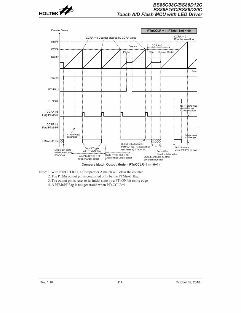
Rev. 1.10 114 October 09, 2018 Rev. 1.10 115 October 09, 2018
BS86C08C/BS86D12CBS86E16C/BS86D20C
Touch A/D Flash MCU with LED Driver
BS86C08C/BS86D12CBS86E16C/BS86D20CTouch A/D Flash MCU with LED Driver
Counter Value
0x3FF
CCRP
CCRA
PTnON
PTnPAU
PTnPOL
CCRP Int. Flag PTMnPF
CCRA Int. Flag PTMnAF
PTMn O/P Pin
Time
CCRA=0
CCRA = 0Counter overflowCCRA > 0 Counter cleared by CCRA value
Pause
Resume
Stop Counter Restart
Output pin set to initial Level Low if PTnOC=0
Output Toggle with PTMnAF flag
Note PTnIO [1:0] = 10 Active High Output select
Here PTnIO [1:0] = 11 Toggle Output select
Output not affected by PTMnAF flag. Remains High until reset by PTnON bit
Output PinReset to Initial value
Output controlled by other pin-shared function
Output Invertswhen PTnPOL is high
PTMnPF not generated
No PTMnAF flag generated on CCRA overflow
Output does not change
PTnCCLR = 1; PTnM [1:0] = 00
Compare Match Output Mode – PTnCCLR=1 (n=0~1)
Note: 1. With PTnCCLR=1, a Comparator A match will clear the counter2. The PTMn output pin is controlled only by the PTMnAF flag3. The output pin is reset to its initial state by a PTnON bit rising edge4. A PTMnPF flag is not generated when PTnCCLR=1
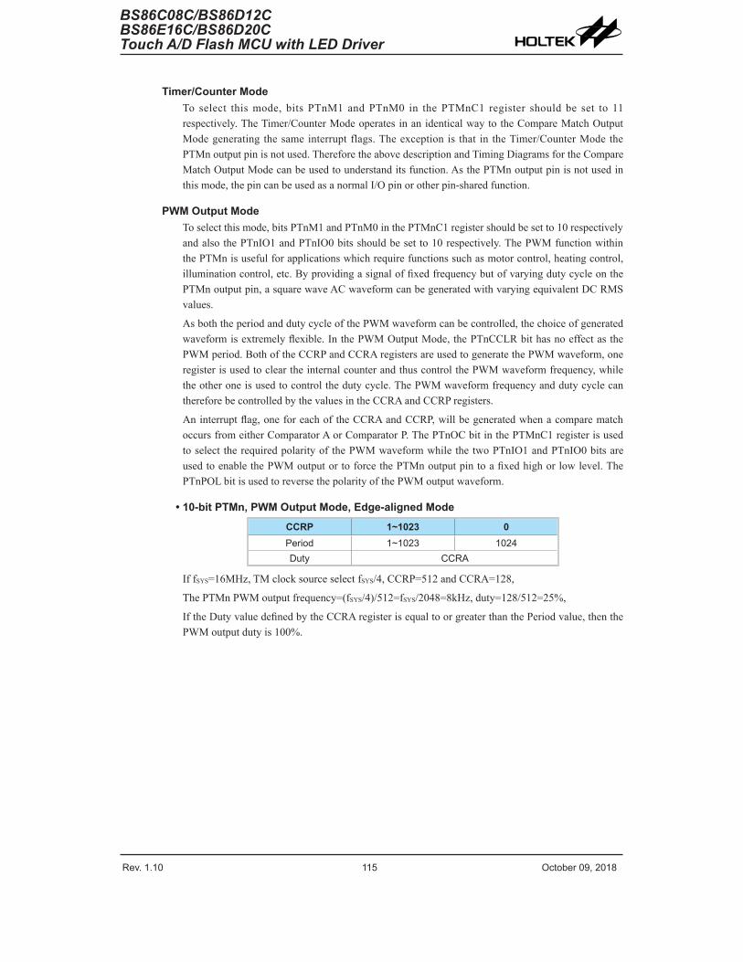
Rev. 1.10 114 October 09, 2018 Rev. 1.10 115 October 09, 2018
BS86C08C/BS86D12CBS86E16C/BS86D20C
Touch A/D Flash MCU with LED Driver
BS86C08C/BS86D12CBS86E16C/BS86D20CTouch A/D Flash MCU with LED Driver
Timer/Counter ModeTo select this mode, bits PTnM1 and PTnM0 in the PTMnC1 register should be set to 11 respectively. The Timer/Counter Mode operates in an identical way to the Compare Match Output Mode generating the same interrupt flags. The exception is that in the Timer/Counter Mode the PTMn output pin is not used. Therefore the above description and Timing Diagrams for the Compare Match Output Mode can be used to understand its function. As the PTMn output pin is not used in this mode, the pin can be used as a normal I/O pin or other pin-shared function.
PWM Output ModeTo select this mode, bits PTnM1 and PTnM0 in the PTMnC1 register should be set to 10 respectively and also the PTnIO1 and PTnIO0 bits should be set to 10 respectively. The PWM function within the PTMn is useful for applications which require functions such as motor control, heating control, illumination control, etc. By providing a signal of fixed frequency but of varying duty cycle on the PTMn output pin, a square wave AC waveform can be generated with varying equivalent DC RMS values.
As both the period and duty cycle of the PWM waveform can be controlled, the choice of generated waveform is extremely flexible. In the PWM Output Mode, the PTnCCLR bit has no effect as the PWM period. Both of the CCRP and CCRA registers are used to generate the PWM waveform, one register is used to clear the internal counter and thus control the PWM waveform frequency, while the other one is used to control the duty cycle. The PWM waveform frequency and duty cycle can therefore be controlled by the values in the CCRA and CCRP registers.
An interrupt flag, one for each of the CCRA and CCRP, will be generated when a compare match occurs from either Comparator A or Comparator P. The PTnOC bit in the PTMnC1 register is used to select the required polarity of the PWM waveform while the two PTnIO1 and PTnIO0 bits are used to enable the PWM output or to force the PTMn output pin to a fixed high or low level. The PTnPOL bit is used to reverse the polarity of the PWM output waveform.
• 10-bit PTMn, PWM Output Mode, Edge-aligned Mode
CCRP 1~1023 0Period 1~1023 1024Duty CCRA
If fSYS=16MHz, TM clock source select fSYS/4, CCRP=512 and CCRA=128,
The PTMn PWM output frequency=(fSYS/4)/512=fSYS/2048=8kHz, duty=128/512=25%,
If the Duty value defined by the CCRA register is equal to or greater than the Period value, then the PWM output duty is 100%.

Rev. 1.10 116 October 09, 2018 Rev. 1.10 117 October 09, 2018
BS86C08C/BS86D12CBS86E16C/BS86D20C
Touch A/D Flash MCU with LED Driver
BS86C08C/BS86D12CBS86E16C/BS86D20CTouch A/D Flash MCU with LED Driver
Counter Value
CCRP
CCRA
PTnON
PTnPAU
PTnPOL
CCRP Int. Flag PTMnPF
CCRA Int. Flag PTMnAF
PTMn O/P Pin(PTnOC=1)
Time
Counter cleared by CCRP
Pause Resume Counter Stop if PTnON bit low
Counter Reset when PTnON returns high
PWM Duty Cycle set by CCRA
PWM resumes operationOutput controlled by
other pin-shared functionOutput InvertsWhen PTnPOL = 1
PWM Period set by CCRP
PTMn O/P Pin(PTnOC=0)
PTnM [1:0] = 10
PWM Output Mode (n=0~1)
Note: 1. The counter is cleared by CCRP2. A counter clear sets the PWM Period3. The internal PWM function continues running even when PTnIO[1:0]=00 or 014. The PTnCCLR bit has no influence on PWM operation

Rev. 1.10 116 October 09, 2018 Rev. 1.10 117 October 09, 2018
BS86C08C/BS86D12CBS86E16C/BS86D20C
Touch A/D Flash MCU with LED Driver
BS86C08C/BS86D12CBS86E16C/BS86D20CTouch A/D Flash MCU with LED Driver
Single Pulse Output ModeTo select this mode, bits PTnM1 and PTnM0 in the PTMnC1 register should be set to 10 respectively and also the PTnIO1 and PTnIO0 bits should be set to 11 respectively. The Single Pulse Output Mode, as the name suggests, will generate a single shot pulse on the PTMn output pin.
The trigger for the pulse output leading edge is a low to high transition of the PTnON bit, which can be implemented using the application program. However in the Single Pulse Output Mode, the PTnON bit can also be made to automatically change from low to high using the external PTCKn pin, which will in turn initiate the Single Pulse output. When the PTnON bit transitions to a high level, the counter will start running and the pulse leading edge will be generated. The PTnON bit should remain high when the pulse is in its active state. The generated pulse trailing edge will be generated when the PTnON bit is cleared to zero, which can be implemented using the application program or when a compare match occurs from Comparator A.
However a compare match from Comparator A will also automatically clear the PTnON bit and thus generate the Single Pulse output trailing edge. In this way the CCRA value can be used to control the pulse width. A compare match from Comparator A will also generate a PTMn interrupt. The counter can only be reset back to zero when the PTnON bit changes from low to high when the counter restarts. In the Single Pulse Output Mode CCRP is not used. The PTnCCLR is not used in this Mode.
PTnON bit0 1
S/W Command SET“PTnON”
orPTCKn Pin
Transition
PTnON bit1 0
CCRA Trailing Edge
S/W Command CLR“PTnON”
orCCRA Compare Match
PTPn Output Pin
Pulse Width = CCRA Value
CCRA Leading Edge
Single Pulse Generation (n=0~1)

Rev. 1.10 118 October 09, 2018 Rev. 1.10 119 October 09, 2018
BS86C08C/BS86D12CBS86E16C/BS86D20C
Touch A/D Flash MCU with LED Driver
BS86C08C/BS86D12CBS86E16C/BS86D20CTouch A/D Flash MCU with LED Driver
Counter Value
CCRP
CCRA
PTnON
PTnPAU
PTnPOL
CCRP Int. Flag PTMnPF
CCRA Int. Flag PTMnAF
PTMn O/P Pin(PTnOC=1)
Time
Counter stopped by CCRA
PauseResume Counter Stops by
software
Counter Reset when PTnON returns high
Pulse Width set by CCRA
Output Invertswhen PTnPOL = 1
No CCRP Interrupts generated
PTMn O/P Pin(PTnOC=0)
PTCKn pin
Software Trigger
Cleared by CCRA match
PTCKn pin Trigger
Auto. set by PTCKn pin
Software Trigger
Software Clear
Software TriggerSoftware
Trigger
PTnM [1:0] = 10 ; PTnIO [1:0] = 11
Single Pulse Output Mode (n=0~1)
Note: 1. Counter stopped by CCRA2. CCRP is not used3. The pulse triggered by the PTCKn pin or by setting the PTnON bit high4. A PTCKn pin active edge will automatically set the PTnON bit high5. In the Single Pulse Output Mode, PTnIO [1:0] must be set to “11” and cannot be changed

Rev. 1.10 118 October 09, 2018 Rev. 1.10 119 October 09, 2018
BS86C08C/BS86D12CBS86E16C/BS86D20C
Touch A/D Flash MCU with LED Driver
BS86C08C/BS86D12CBS86E16C/BS86D20CTouch A/D Flash MCU with LED Driver
Capture Input ModeTo select this mode bits PTnM1 and PTnM0 in the PTMnC1 register should be set to 01 respectively. This mode enables external signals to capture and store the present value of the internal counter and can therefore be used for applications such as pulse width measurements. The external signal is supplied on the PTPnI or PTCKn pin, selected by the PTnCAPTS bit in the PTMnC1 register. The input pin active edge can be either a rising edge, a falling edge or both rising and falling edges; the active edge transition type is selected using the PTnIO1 and PTnIO0 bits in the PTMnC1 register. The counter is started when the PTnON bit changes from low to high which is initiated using the application program.
When the required edge transition appears on the PTPnI or PTCKn pin the present value in the counter will be latched into the CCRA registers and a PTMn interrupt generated. Irrespective of what events occur on the PTPnI or PTCKn pin the counter will continue to free run until the PTnON bit changes from high to low. When a CCRP compare match occurs the counter will reset back to zero; in this way the CCRP value can be used to control the maximum counter value. When a CCRP compare match occurs from Comparator P, a PTMn interrupt will also be generated. Counting the number of overflow interrupt signals from the CCRP can be a useful method in measuring long pulse widths. The PTnIO1 and PTnIO0 bits can select the active trigger edge on the PTPnI or PTCKn pin to be a rising edge, falling edge or both edge types. If the PTnIO1 and PTnIO0 bits are both set high, then no capture operation will take place irrespective of what happens on the PTPnI or PTCKn pin, however it must be noted that the counter will continue to run.
As the PTPnI or PTCKn pin is pin shared with other functions, care must be taken if the PTMn is in the Input Capture Mode. This is because if the pin is setup as an output, then any transitions on this pin may cause an input capture operation to be executed. The PTnCCLR, PTnOC and PTnPOL bits are not used in this Mode.

Rev. 1.10 120 October 09, 2018 Rev. 1.10 121 October 09, 2018
BS86C08C/BS86D12CBS86E16C/BS86D20C
Touch A/D Flash MCU with LED Driver
BS86C08C/BS86D12CBS86E16C/BS86D20CTouch A/D Flash MCU with LED Driver
Counter Value
YY
CCRP
PTnON
PTnPAU
CCRP Int. Flag PTMnPF
CCRA Int. Flag PTMnAF
CCRA Value
Time
Counter cleared by CCRP
PauseResume
Counter Reset
PTnM[1:0] = 01
PTMn Capture PinPTPnI or PTCKn
XX
Counter Stop
PTnIO [1:0] Value
Active edge
Activeedge Active edge
00 - Rising edge 01 - Falling edge 10 - Both edges 11 - Disable Capture
XX YY XX YY
Capture Input Mode (n=0~1)
Note: 1. PTnM[1:0]=01 and active edge set by the PTnIO[1:0] bits2. A PTMn Capture input pin active edge transfers the counter value to CCRA3. PTnCCLR bit not used4. No output function – PTnOC and PTnPOL bits are not used5. CCRP determines the counter value and the counter has a maximum count value when CCRP is equal to
zero
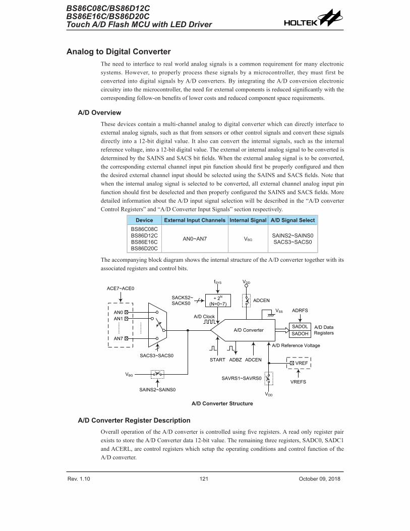
Rev. 1.10 120 October 09, 2018 Rev. 1.10 121 October 09, 2018
BS86C08C/BS86D12CBS86E16C/BS86D20C
Touch A/D Flash MCU with LED Driver
BS86C08C/BS86D12CBS86E16C/BS86D20CTouch A/D Flash MCU with LED Driver
Analog to Digital ConverterThe need to interface to real world analog signals is a common requirement for many electronic systems. However, to properly process these signals by a microcontroller, they must first be converted into digital signals by A/D converters. By integrating the A/D conversion electronic circuitry into the microcontroller, the need for external components is reduced significantly with the corresponding follow-on benefits of lower costs and reduced component space requirements.
A/D OverviewThese devices contain a multi-channel analog to digital converter which can directly interface to external analog signals, such as that from sensors or other control signals and convert these signals directly into a 12-bit digital value. It also can convert the internal signals, such as the internal reference voltage, into a 12-bit digital value. The external or internal analog signal to be converted is determined by the SAINS and SACS bit fields. When the external analog signal is to be converted, the corresponding external channel input pin function should first be properly configured and then the desired external channel input should be selected using the SAINS and SACS fields. Note that when the internal analog signal is selected to be converted, all external channel analog input pin function should first be deselected and then properly configured the SAINS and SACS fields. More detailed information about the A/D input signal selection will be described in the “A/D converter Control Registers” and “A/D Converter Input Signals” section respectively.
Device External Input Channels Internal Signal A/D Signal SelectBS86C08CBS86D12CBS86E16CBS86D20C
AN0~AN7 VBGSAINS2~SAINS0SACS3~SACS0
The accompanying block diagram shows the internal structure of the A/D converter together with its associated registers and control bits.
ACE7~ACE0
SACS3~SACS0
A/D Converter
START ADBZ ADCEN
VSS
÷ 2N
(N=0~7)
fSYS
SACKS2~SACKS0
VDD
VDD
SAVRS1~SAVRS0
ADCEN
A/D Reference Voltage
A/D DataRegisters
ADRFS
SADOLSADOH
A/D Clock
VREFS
AN0
AN7
AN1
VREF
VBG
SAINS2~SAINS0
A/D Converter Structure
A/D Converter Register DescriptionOverall operation of the A/D converter is controlled using five registers. A read only register pair exists to store the A/D Converter data 12-bit value. The remaining three registers, SADC0, SADC1 and ACERL, are control registers which setup the operating conditions and control function of the A/D converter.

Rev. 1.10 122 October 09, 2018 Rev. 1.10 123 October 09, 2018
BS86C08C/BS86D12CBS86E16C/BS86D20C
Touch A/D Flash MCU with LED Driver
BS86C08C/BS86D12CBS86E16C/BS86D20CTouch A/D Flash MCU with LED Driver
Register NameBit
7 6 5 4 3 2 1 0SADOL (ADRFS=0) D3 D2 D1 D0 — — — —SADOL (ADRFS=1) D7 D6 D5 D4 D3 D2 D1 D0SADOH (ADRFS=0) D11 D10 D9 D8 D7 D6 D5 D4SADOH (ADRFS=1) — — — — D11 D10 D9 D8SADC0 START ADBZ ADCEN ADRFS SACS3 SACS2 SACS1 SACS0SADC1 SAINS2 SAINS1 SAINS0 SAVRS1 SAVRS0 SACKS2 SACKS1 SACKS0ACERL ACE7 ACE6 ACE5 ACE4 ACE3 ACE2 ACE1 ACE0
A/D Converter Register List
A/D Converter Data Registers – SADOL, SADOHAs these devices contain an internal 12-bit A/D converter, it requires two data registers to store the converted value. These are a high byte register, known as SADOH, and a low byte register, known as SADOL. After the conversion process takes place, these registers can be directly read by the microcontroller to obtain the digitised conversion value. As only 12 bits of the 16-bit register space is utilised, the format in which the data is stored is controlled by the ADRFS bit in the SADC0 register as shown in the accompanying table. D0~D11 are the A/D conversion result data bits. Any unused bits will be read as zero. The A/D data registers contents will be unchanged if the A/D converter is disabled.
ADRFSSADOH SADOL
7 6 5 4 3 2 1 0 7 6 5 4 3 2 1 00 D11 D10 D9 D8 D7 D6 D5 D4 D3 D2 D1 D0 0 0 0 01 0 0 0 0 D11 D10 D9 D8 D7 D6 D5 D4 D3 D2 D1 D0
A/D Converter Data Registers
A/D Converter Control Registers – SADC0, SADC1, ACERLTo control the function and operation of the A/D converter, three control registers known as SADC0, SADC1 and ACERL are provided. These 8-bit registers define functions such as the selection of which analog signal is connected to the internal A/D converter, the digitised data format, the A/D clock source as well as controlling the start function and monitoring the A/D converter busy status. As these devices contain only one actual analog to digital converter hardware circuit, each of the external and internal analog signals must be routed to the converter. The SACS3~SACS0 bits in the SADC0 register are used to determine which external channel input is selected to be converted. The SAINS2~SAINS0 bits in the SADC1 register are used to determine that the analog signal to be converted comes from the internal analog signal or external analog channel input.
The ACERL register contains the ACE7~ACE0 bits which determine which pins on I/O Ports are used as analog inputs for the A/D converter input and which pins are not. Setting the corresponding bit high will select the A/D input function while clearing the bit to zero will select either the I/O or other pin-shared function. When the pin is selected to be an A/D input, its original function whether it is an I/O or other pin-shared function will be removed. In addition, any internal pull-high resistor connected to the pin will be automatically removed if the pin is selected to be an A/D converter input.

Rev. 1.10 122 October 09, 2018 Rev. 1.10 123 October 09, 2018
BS86C08C/BS86D12CBS86E16C/BS86D20C
Touch A/D Flash MCU with LED Driver
BS86C08C/BS86D12CBS86E16C/BS86D20CTouch A/D Flash MCU with LED Driver
• SADC0 Register
Bit 7 6 5 4 3 2 1 0Name START ADBZ ADCEN ADRFS SACS3 SACS2 SACS1 SACS0R/W R/W R R/W R/W R/W R/W R/W R/WPOR 0 0 0 0 0 0 0 0
Bit 7 START: Start the A/D Conversion0→1→0: Start
This bit is used to initiate an A/D conversion process. The bit is normally low but if set high and then cleared low again, the A/D converter will initiate a conversion process.
Bit 6 ADBZ: A/D Converter busy flag0: No A/D conversion is in progress1: A/D conversion is in progress
This read only flag is used to indicate whether the A/D conversion is in progress or not. When the START bit is set from low to high and then to low again, the ADBZ flag will be set to 1 to indicate that the A/D conversion is initiated. The ADBZ flag will be cleared to 0 after the A/D conversion is complete.
Bit 5 ADCEN: A/D Converter function enable control0: Disable1: Enable
This bit controls the A/D internal function. This bit should be set to one to enable the A/D converter. If the bit is set low, then the A/D converter will be switched off reducing the device power consumption. When the A/D converter function is disabled, the contents of the A/D data register pair known as SADOH and SADOL will be unchanged.
Bit 4 ADRFS: A/D conversion data format select0: A/D converter data format → SADOH=D [11:4]; SADOL=D [3:0]1: A/D converter data format → SADOH=D [11:8]; SADOL=D [7:0]
This bit controls the format of the 12-bit converted A/D value in the two A/D data registers. Details are provided in the A/D converter data register section.
Bit 3~0 SACS3~SACS0: A/D converter external analog input channel select0000: External AN0 input0001: External AN1 input0010: External AN2 input0011: External AN3 input0100: External AN4 input0101: External AN5 input0110: External AN6 input0111: External AN7 input1xxx: Non-existed channel, input floating if selected
These bits are used to select which external analog input channel is to be converted. When the external analog input channel is selected, the SAINS bit field must be set to “000”, “101” or “11x”. Details are summarized in the “A/D Converter Input Signal Selection” table.

Rev. 1.10 124 October 09, 2018 Rev. 1.10 125 October 09, 2018
BS86C08C/BS86D12CBS86E16C/BS86D20C
Touch A/D Flash MCU with LED Driver
BS86C08C/BS86D12CBS86E16C/BS86D20CTouch A/D Flash MCU with LED Driver
• SADC1 Register
Bit 7 6 5 4 3 2 1 0Name SAINS2 SAINS1 SAINS0 SAVRS1 SAVRS0 SACKS2 SACKS1 SACKS0R/W R/W R/W R/W R/W R/W R/W R/W R/WPOR 0 0 0 0 0 0 0 0
Bit 7~5 SAINS2~SAINS0: A/D converter input signal select000: External source – External analog channel input, ANn001: Internal source – Internal bandgap reference voltage, VBG
010~100: Internal source – Reserved, connected to ground101~111: External source – External analog channel input, ANn
Care must be taken if the SAINS field is set to “001” to select the internal analog signal to be converted. When the internal analog signal is selected to be converted, the external channel input pin must never be selected as the A/D input signal by properly setting the SACS bit field with a value of “1xxx”. Otherwise, the external channel input will be connected together with the internal analog signal. This will result in unpredictable situations such as an irreversible damage.
Bit 4~3 SAVRS1~SAVRS0: A/D converter reference voltage select00: External VREF pin01: Internal A/D converter power, VDD
1x: External VREF pinThese bits are used to select the A/D converter reference voltage source. Care must be taken if the SAVRS field is set to “01” to select the internal A/D converter power voltage as the reference voltage source. When the internal reference voltage source is selected, the external VREF cannot be configured as the reference voltage input by properly configuring the VREFS bit in the TMPC register. Otherwise, the external input voltage on the VREF pin will be connected to the internal A/D converter power. This will result in unpredictable situations.
Bit 2~0 SACKS2~SACKS0: A/D conversion clock source select000: fSYS
001: fSYS/2010: fSYS/4011: fSYS/8100: fSYS/16101: fSYS/32110: fSYS/64111: fSYS/128
These bits are used to select the clock source for the A/D converter.
• ACERL Register
Bit 7 6 5 4 3 2 1 0Name ACE7 ACE6 ACE5 ACE4 ACE3 ACE2 ACE1 ACE0R/W R/W R/W R/W R/W R/W R/W R/W R/WPOR 0 0 0 0 0 0 0 0
Bit 7 ACE7: AN7 input pin enable control0: Disable – not A/D input1: Enable – A/D input, AN7
Bit 6 ACE6: AN6 input pin enable control0: Disable – not A/D input1: Enable – A/D input, AN6
Bit 5 ACE5: AN5 input pin enable control0: Disable – not A/D input1: Enable – A/D input, AN5

Rev. 1.10 124 October 09, 2018 Rev. 1.10 125 October 09, 2018
BS86C08C/BS86D12CBS86E16C/BS86D20C
Touch A/D Flash MCU with LED Driver
BS86C08C/BS86D12CBS86E16C/BS86D20CTouch A/D Flash MCU with LED Driver
Bit 4 ACE4: AN4 input pin enable control0: Disable – not A/D input1: Enable – A/D input, AN4
Note that for the BS86C08C/BS86D12C/BS86E16C device, as the AN4 pin is pin-shared with the VREF pin function, if the VREFS bit in the TMPC register is set high, the VREF pin will be selected and the AN4 pin function will be disabled automatically.
Bit 3 ACE3: AN3 input pin enable control0: Disable – not A/D input1: Enable – A/D input, AN3
Bit 2 ACE2: AN2 input pin enable control0: Disable – not A/D input1: Enable – A/D input, AN2
Bit 1 ACE1: AN1 input pin enable control0: Disable – not A/D input1: Enable – A/D input, AN1
Bit 0 ACE0: AN0 input pin enable control0: Disable – not A/D input1: Enable – A/D input, AN0
Note that for the BS86D20C device, as the AN0 pin is pin-shared with the VREF pin function, if the VREFS bit in the TMPC register is set high, the VREF pin will be selected and the AN0 pin function will be disabled automatically.
A/D Converter Reference VoltageThe actual reference voltage supply to the A/D Converter can be supplied from the positive power supply, VDD, or an external reference source supplied on pin VREF determined by the SAVRS bit field in the SADC1 register. When the SAVRS field is set to “01”, the A/D converter reference voltage will come from the VDD. Otherwise, the A/D converter reference voltage will come from the VREF pin if the SAVRS field is set to any other value except “01”. When the VREF pin is selected as the reference voltage supply pin, the VREFS bit in the TMPC register should first be properly configured to enable the VREF pin function as it is pin-shared with other functions. However, if the internal A/D converter power is selected as the reference voltage, the external VREF pin must not be configured as the reference voltage input function to avoid the internal connection between the VREF pin to the internal A/D converter power. Note that the analog input values must not be allowed to exceed the value of the selected reference voltage.
A/D Converter Input SignalsAll of the external A/D analog input pins are pin-shared with the I/O pins as well as other functions. The corresponding pin-shared function control bits ACEn in the ACERL register determine whether the external input pins are setup as A/D converter analog channel inputs or whether they have other functions. If the corresponding pin is setup to be an A/D converter analog channel input by setting the ACEn bit high, the original pin function will be disabled. In this way, pins can be changed under program control to change their function between A/D inputs and other functions. All pull-high resistors, which are setup through register programming, will be automatically disconnected if the pins are setup as A/D inputs. Note that it is not necessary to first setup the A/D pin as an input in the port control register to enable the A/D input as when the relevant A/D input function selection bits enable an A/D input, the status of the port control register will be overridden.
As these devices contain only one actual analog to digital converter hardware circuit, one of the external or internal analog signals must be routed to the converter. The SAINS2~SAINS0 bits in the SADC1 register are used to determine that the analog signal to be converted comes from the external channel input or internal analog signal. The SACS3~SACS0 bits in the SADC0 register are
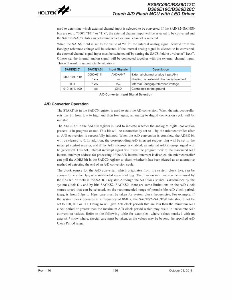
Rev. 1.10 126 October 09, 2018 Rev. 1.10 127 October 09, 2018
BS86C08C/BS86D12CBS86E16C/BS86D20C
Touch A/D Flash MCU with LED Driver
BS86C08C/BS86D12CBS86E16C/BS86D20CTouch A/D Flash MCU with LED Driver
used to determine which external channel input is selected to be converted. If the SAINS2~SAINS0 bits are set to “000”, “101” or “11x”, the external channel input will be selected to be converted and the SACS3~SACS0 bits can determine which external channel is selected.
When the SAINS field is set to the value of “001”, the internal analog signal derived from the Bandgap reference voltage will be selected. If the internal analog signal is selected to be converted, the external channel signal input must be switched off by setting the SACS field to a value of “1xxx”. Otherwise, the internal analog signal will be connected together with the external channel input. This will result in unpredictable situations.
SAINS[2:0] SACS[3:0] Input Signals Description
000, 101, 11x0000~0111 AN0~AN7 External channel analog input ANn
1xxx — Floating, no external channel is selected001 1xxx VBG Internal Bandgap reference voltage
010, 011, 100 1xxx GND Connected to the ground
A/D Converter Input Signal Selection
A/D Converter OperationThe START bit in the SADC0 register is used to start the AD conversion. When the microcontroller sets this bit from low to high and then low again, an analog to digital conversion cycle will be initiated.
The ADBZ bit in the SADC0 register is used to indicate whether the analog to digital conversion process is in progress or not. This bit will be automatically set to 1 by the microcontroller after an A/D conversion is successfully initiated. When the A/D conversion is complete, the ADBZ bit will be cleared to 0. In addition, the corresponding A/D interrupt request flag will be set in the interrupt control register, and if the A/D interrupt is enabled, an internal A/D interrupt signal will be generated. This A/D internal interrupt signal will direct the program flow to the associated A/D internal interrupt address for processing. If the A/D internal interrupt is disabled, the microcontroller can poll the ADBZ bit in the SADC0 register to check whether it has been cleared as an alternative method of detecting the end of an A/D conversion cycle.
The clock source for the A/D converter, which originates from the system clock fSYS, can be chosen to be either fSYS or a subdivided version of fSYS. The division ratio value is determined by the SACKS bit field in the SADC1 register. Although the A/D clock source is determined by the system clock fSYS and by bits SACKS2~SACKS0, there are some limitations on the A/D clock source speed that can be selected. As the recommended range of permissible A/D clock period, tADCK, is from 0.5μs to 10μs, care must be taken for system clock frequencies. For example, if the system clock operates at a frequency of 8MHz, the SACKS2~SACKS0 bits should not be set to 000, 001 or 111. Doing so will give A/D clock periods that are less than the minimum A/D clock period or greater than the maximum A/D clock period which may result in inaccurate A/D conversion values. Refer to the following table for examples, where values marked with an asterisk * show where, special care must be taken, as the values may be beyond the specified A/D Clock Period range.

Rev. 1.10 126 October 09, 2018 Rev. 1.10 127 October 09, 2018
BS86C08C/BS86D12CBS86E16C/BS86D20C
Touch A/D Flash MCU with LED Driver
BS86C08C/BS86D12CBS86E16C/BS86D20CTouch A/D Flash MCU with LED Driver
fSYS
A/D Clock Period (tADCK)SACKS[2:0]
=000(fSYS)
SACKS[2:0]=001
(fSYS/2)
SACKS[2:0]=010
(fSYS/4)
SACKS[2:0]=011
(fSYS/8)
SACKS[2:0]=100
(fSYS/16)
SACKS[2:0]=101
(fSYS/32)
SACKS[2:0]=110
(fSYS/64)
SACKS[2:0]=111
(fSYS/128)1MHz 1μs 2μs 4μs 8μs 16μs* 32μs* 64μs* 128μs*2MHz 500ns 1μs 2μs 4μs 8μs 16μs* 32μs* 64μs*4MHz 250ns* 500ns 1μs 2μs 4μs 8μs 16μs* 32μs*8MHz 125ns* 250ns* 500ns 1μs 2μs 4μs 8μs 16μs*
12MHz 83ns* 167ns* 333ns* 667ns 1.33μs 2.67μs 5.33μs 10.67μs*16MHz 62.5ns* 125ns* 250ns* 500ns 1μs 2μs 4μs 8μs
A/D Clock Period Examples
Controlling the power on/off function of the A/D converter circuitry is implemented using the ADCEN bit in the SADC0 register. This bit must be set high to power on the A/D converter. When the ADCEN bit is set high to power on the A/D converter internal circuitry, a certain delay, as indicated in the timing diagram, must be allowed before an A/D conversion is initiated. Even if no pins are selected for use as A/D inputs by clearing the ACE7~ACE0 bits in the ACERL register, if the ADCEN bit is high, then some power will still be consumed. In power conscious applications it is therefore recommended that the ADCEN is set low to reduce power consumption when the A/D converter function is not being used.
Conversion Rate and Timing DiagramA complete A/D conversion contains two parts, data sampling and data conversion. The data sampling which is defined as tADS takes 4 A/D clock cycles and the data conversion takes 12 A/D clock cycles. Therefore a total of 16 A/D clock cycles for an analog signal A/D conversion which is defined as tADC are necessary.
Maximum single A/D conversion rate=A/D clock period / 16
The accompanying diagram shows graphically the various stages involved in an external channel input signal analog to digital conversion process and its associated timing. After an A/D conversion process has been initiated by the application program, the microcontroller internal hardware will begin to carry out the conversion, during which time the program can continue with other functions. The time taken for the A/D conversion is 16 tADCK clock cycles where tADCK is equal to the A/D clock period.
ADCEN
START
ADBZ
SACS[3:0](SAINS[2:0]=000)
off on off on
tON2ST
tADS
A/D sampling timetADS
A/D sampling time
Start of A/D conversion Start of A/D conversion Start of A/D conversion
End of A/D conversion
End of A/D conversion
tADC
A/D conversion timetADC
A/D conversion timetADC
A/D conversion time
0011B 0010B 0000B 0001B
A/D channel switch
A/D Conversion Timing – External Channel Input
Rev. 1.10 128 October 09, 2018 Rev. 1.10 129 October 09, 2018
BS86C08C/BS86D12CBS86E16C/BS86D20C
Touch A/D Flash MCU with LED Driver
BS86C08C/BS86D12CBS86E16C/BS86D20CTouch A/D Flash MCU with LED Driver
Summary of A/D Conversion StepsThe following summarises the individual steps that should be executed in order to implement an A/D conversion process.
• Step 1Select the required A/D conversion clock by properly programming the SACKS2~SACKS0 bits in the SADC1 register.
• Step 2Enable the A/D converter by setting the ADCEN bit in the SADC0 register to one.
• Step 3Select which signal is to be connected to the internal A/D converter by correctly configuring the SACS and SAINS bit fieldsSelecting the external channel input to be converted, go to Step 4.Selecting the internal analog signal to be converted, go to Step 5.
• Step 4If the SAINS field is 000, 101 or 11x, the external channel input can be selected. The desired external channel input is selected by configuring the SACS field. When the A/D input signal comes from the external channel input, the corresponding pin should be configured as an A/D input function by selecting the relevant function control bits, ACEn. Then go to Step 6.
• Step 5If the SAINS field is set to 001, the relevant internal analog signal can be selected. Before the A/D input signal is selected to come from the internal analog signal by properly configuring the SAINS field, the SACS field must be set to “1xxx” to select a non-existed channel input. Then go to Step 6.
• Step 6Select the A/D converter output data format by configuring the ADRFS bit in the SADC0 register.
• Step 7Select the A/D converter reference voltage source by configuring the SAVRS bit field in the SADC1 register. If the internal reference voltage is selected, the external reference input pin function must be disabled by properly configuring the VREFS bit in the TMPC register.
• Step 8If A/D conversion interrupt is used, the interrupt control registers must be correctly configured to ensure the A/D interrupt function is active. The master interrupt control bit, EMI, and the A/D conversion interrupt control bit, ADE, must both be set high in advance.
• Step 9The A/D conversion procedure can now be initialized by setting the START bit from low to high and then low again.
• Step 10If A/D conversion is in progress, the ADBZ flag will be set high. After the A/D conversion process is complete, the ADBZ flag will go low and then the output data can be read from SADOH and SADOL registers.
Note: When checking for the end of the conversion process, if the method of polling the ADBZ bit in the SADC0 register is used, the interrupt enable step above can be omitted.
Programming ConsiderationsDuring microcontroller operations where the A/D converter is not being used, the A/D internal circuitry can be switched off to reduce power consumption, by clearing bit ADCEN to zero in the

Rev. 1.10 128 October 09, 2018 Rev. 1.10 129 October 09, 2018
BS86C08C/BS86D12CBS86E16C/BS86D20C
Touch A/D Flash MCU with LED Driver
BS86C08C/BS86D12CBS86E16C/BS86D20CTouch A/D Flash MCU with LED Driver
SADC0 register. When this happens, the internal A/D converter circuits will not consume power irrespective of what analog voltage is applied to their input lines. If the A/D converter input lines are used as normal I/Os, then care must be taken as if the input voltage is not at a valid logic level, then this may lead to some increase in power consumption.
A/D Transfer FunctionAs the devices contain a 12-bit A/D converter, its full-scale converted digitised value is equal to FFFH. Since the full-scale analog input value is equal to the actual A/D converter reference voltage, VREF, this gives a single bit analog input value of reference voltage value divided by 4096.
1 LSB=VREF÷4096
The A/D Converter input voltage value can be calculated using the following equation:
A/D input voltage=A/D output digital value×(VREF÷4096)
The diagram shows the ideal transfer function between the analog input value and the digitised output value for the A/D converter. Except for the digitised zero value, the subsequent digitised values will change at a point 0.5 LSB below where they would change without the offset, and the last full scale digitised value will change at a point 1.5 LSB below the VREF level. Note that here the VREF voltage is the actual A/D converter reference voltage source determined by the SAVRS field.
FFFH
FFEH
FFDH
03H
02H
01H
0 1 2 3 4093 4094 4095 4096
VREF4096
Analog Input Voltage
A/D Conversion Result
1.5 LSB
0.5 LSB
Ideal A/D Transfer Function
A/D Programming ExamplesThe following two programming examples illustrate how to setup and implement an A/D conversion. In the first example, the method of polling the ADBZ bit in the SADC0 register is used to detect when the conversion cycle is complete, whereas in the second example, the A/D interrupt is used to determine when the conversion is complete.
Example: using an ADBZ polling method to detect the end of conversionclr ADE ; disable ADC interruptmov a,03H ; select fSYS/8 as A/D clock and A/D inputmovSADC1,a ;signalcomesfromexternalchannel ;selectVREFpinvoltageasA/Dreferencevoltagesourcemov a,01HmovSADC0,a ;andAN1isselectedastheexternalchannelinputsetADCEN ;enabletheA/Dconvertermova,02H ;setupACERLtoconfigurepinAN1asanaloginputmovACERL,a

Rev. 1.10 130 October 09, 2018 Rev. 1.10 131 October 09, 2018
BS86C08C/BS86D12CBS86E16C/BS86D20C
Touch A/D Flash MCU with LED Driver
BS86C08C/BS86D12CBS86E16C/BS86D20CTouch A/D Flash MCU with LED Driver
:start_conversion:clrSTART ;highpulseonstartbittoinitiateconversionsetSTART ;resetA/DclrSTART ;startA/D:polling_EOC:szADBZ ;polltheSADC0registerADBZbittodetectendofA/Dconversionjmppolling_EOC ;continuepollingmova,SADOL ;readlowbyteconversionresultvaluemovSADOL_buffer,a ;saveresulttouserdefinedregistermova,SADOH ;readhighbyteconversionresultvaluemovSADOH_buffer,a ;saveresulttouserdefinedregister:jmpstart_conversion ;startnextA/Dconversion
Example: using the interrupt method to detect the end of conversionclr ADE ; disable ADC interruptmov a,03H ; select fSYS/8 as A/D clock and A/D inputmovSADC1,a ;signalcomesfromexternalchannel ;selectVREFpinvoltageasA/Dreferencevoltagesourcemov a,01HmovSADC0,a ;andAN1isselectedastheexternalchannelinputsetADCEN ;enabletheA/Dconvertermova,02H ;setupACERLtoconfigurepinAN1asanaloginputmovACERL,a:Start_conversion:clrSTART ;highpulseonSTARTbittoinitiateconversionsetSTART ;resetA/DclrSTART ;startA/DclrADF ;clearADCinterruptrequestflagset ADE ; enable ADC interruptsetEMI ;enableglobalinterrupt::ADC_ISR: ;ADCinterruptserviceroutinemovacc_stack,a ;saveACCtouserdefinedmemorymova,STATUSmovstatus_stack,a ;saveSTATUStouserdefinedmemory:mova,SADOL ;readlowbyteconversionresultvaluemovSADOL_buffer,a ;saveresulttouserdefinedregistermova,SADOH ;readhighbyteconversionresultvaluemovSADOH_buffer,a ;saveresulttouserdefinedregister:EXIT_INT_ISR:mova,status_stackmovSTATUS,a ;restoreSTATUSfromuserdefinedmemorymova,acc_stack ;restoreACCfromuserdefinedmemoryreti

Rev. 1.10 130 October 09, 2018 Rev. 1.10 131 October 09, 2018
BS86C08C/BS86D12CBS86E16C/BS86D20C
Touch A/D Flash MCU with LED Driver
BS86C08C/BS86D12CBS86E16C/BS86D20CTouch A/D Flash MCU with LED Driver
Touch Key FunctionEach device provides multiple touch key functions. The touch key function is fully integrated and requires no external components, allowing touch key functions to be implemented by the simple manipulation of internal registers.
Touch Key StructureThe touch keys are pin-shared with the I/O pins, with the desired function chosen via the corresponding selection register bits. Keys are organised into several groups, with each group known as a module and having a module number, M0 to Mn. Each module is a fully independent set of four Touch Keys and each Touch Key has its own oscillator. Each module contains its own control logic circuits and register set. Examination of the register names will reveal the module number it is referring to.
Device Total Key Number Touch Key Module Touch Key
BS86C08C 8 Mn(n=0~1)
M0 KEY1~KEY4M1 KEY5~KEY8
BS86D12C 12 Mn(n=0~2)
M0 KEY1~KEY4M1 KEY5~KEY8M2 KEY9~KEY12
BS86E16C 16 Mn(n=0~3)
M0 KEY1~KEY4M1 KEY5~KEY8M2 KEY9~KEY12M3 KEY13~KEY16
BS86D20C 20 Mn(n=0~4)
M0 KEY1~KEY4M1 KEY5~KEY8M2 KEY9~KEY12M3 KEY13~KEY16M4 KEY17~KEY20
Touch Key Structure

Rev. 1.10 132 October 09, 2018 Rev. 1.10 133 October 09, 2018
BS86C08C/BS86D12CBS86E16C/BS86D20C
Touch A/D Flash MCU with LED Driver
BS86C08C/BS86D12CBS86E16C/BS86D20CTouch A/D Flash MCU with LED Driver
Touch Key Register DefinitionEach touch key module, which contains four touch key functions, has its own suite registers. The following table shows the register set for each touch key module. The Mn within the register name refers to the Touch Key module number. The series of devices has up to five Touch Key Modules dependent upon the selected device.
Register Name DescriptionTKTMR Touch key time slot 8-bit counter preload registerTKC0 Touch key function Control register 0TKC1 Touch key function Control register 1TK16DL Touch key function 16-bit counter low byteTK16DH Touch key function 16-bit counter high byteTKMn16DL Touch key module n 16-bit C/F counter low byteTKMn16DH Touch key module n 16-bit C/F counter high byteTKMnROL Touch key module n reference oscillator capacitor select low byteTKMnROH Touch key module n reference oscillator capacitor select high byteTKMnC0 Touch key module n Control register 0TKMnC1 Touch key module n Control register 1
Touch Key Function Register Definition (n=0~4)
Register Name
Bit
7 6 5 4 3 2 1 0TKTMR D7 D6 D5 D4 D3 D2 D1 D0TKC0 — TKRCOV TKST TKCFOV TK16OV TSCS TK16S1 TK16S0TKC1 — — — — — — TKFS1 TKFS0TK16DL D7 D6 D5 D4 D3 D2 D1 D0TK16DH D15 D14 D13 D12 D11 D10 D9 D8TKMn16DL D7 D6 D5 D4 D3 D2 D1 D0TKMn16DH D15 D14 D13 D12 D11 D10 D9 D8TKMnROL D7 D6 D5 D4 D3 D2 D1 D0TKMnROH — — — — — — D9 D8TKMnC0 MnMXS1 MnMXS0 MnDFEN MnFILEN MnSOFC MnSOF2 MnSOF1 MnSOF0TKMnC1 MnTSS — MnROEN MnKOEN MnK4IO MnK3IO MnK2IO MnK1IO
Touch Key Function Register List (n=0~4)
• TKTMR Register
Bit 7 6 5 4 3 2 1 0Name D7 D6 D5 D4 D3 D2 D1 D0R/W R/W R/W R/W R/W R/W R/W R/W R/WPOR 0 0 0 0 0 0 0 0
Bit 7~0 D7~D0: Touch key time slot 8-bit counter preload registerThe touch key time slot counter preload register is used to determine the touch key time slot overflow time. The time slot unit period is obtained by a 5-bit counter and equal to 32 time slot clock cycles. Therefore, the time slot counter overflow time is equal to the following equation shown.Time slot counter overflow time=(256–TKTMR[7:0])×32 tTSC, where tTSC is the time slot counter clock period.
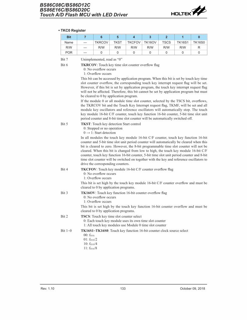
Rev. 1.10 132 October 09, 2018 Rev. 1.10 133 October 09, 2018
BS86C08C/BS86D12CBS86E16C/BS86D20C
Touch A/D Flash MCU with LED Driver
BS86C08C/BS86D12CBS86E16C/BS86D20CTouch A/D Flash MCU with LED Driver
• TKC0 Register
Bit 7 6 5 4 3 2 1 0Name — TKRCOV TKST TKCFOV TK16OV TSCS TK16S1 TK16S0R/W — R/W R/W R/W R/W R/W R/W RPOR — 0 0 0 0 0 0 0
Bit 7 Unimplemented, read as “0”Bit 6 TKRCOV: Touch key time slot counter overflow flag
0: No overflow occurs1: Overflow occurs
This bit can be accessed by application program. When this bit is set by touch key time slot counter overflow, the corresponding touch key interrupt request flag will be set. However, if this bit is set by application program, the touch key interrupt request flag will not be affected. Therefore, this bit cannot be set by application program but must be cleared to 0 by application program.If the module 0 or all module time slot counter, selected by the TSCS bit, overflows, the TKRCOV bit and the Touch Key Interrupt request flag, TKMF, will be set and all module key oscillators and reference oscillators will automatically stop. The touch key module 16-bit C/F counter, touch key function 16-bit counter, 5-bit time slot unit period counter and 8-bit time slot counter will be automatically switched off.
Bit 5 TKST: Touch key detection Start control0: Stopped or no operation0 → 1: Start detection
In all modules the touch key module 16-bit C/F counter, touch key function 16-bit counter and 5-bit time slot unit period counter will automatically be cleared when this bit is cleared to zero. However, the 8-bit programmable time slot counter will not be cleared. When this bit is changed from low to high, the touch key module 16-bit C/F counter, touch key function 16-bit counter, 5-bit time slot unit period counter and 8-bit time slot counter will be switched on together with the key and reference oscillators to drive the corresponding counters.
Bit 4 TKCFOV: Touch key module 16-bit C/F counter overflow flag0: No overflow occurs1: Overflow occurs
This bit is set high by the touch key module 16-bit C/F counter overflow and must be cleared to 0 by application programs.
Bit 3 TK16OV: Touch key function 16-bit counter overflow flag0: No overflow occurs1: Overflow occurs
This bit is set high by the touch key function 16-bit counter overflow and must be cleared to 0 by application programs.
Bit 2 TSCS: Touch key time slot counter select0: Each touch key module uses its own time slot counter1: All touch key modules use Module 0 time slot counter
Bit 1~0 TK16S1~TK16S0: Touch key function 16-bit counter clock source select00: fSYS
01: fSYS/210: fSYS/411: fSYS/8

Rev. 1.10 134 October 09, 2018 Rev. 1.10 135 October 09, 2018
BS86C08C/BS86D12CBS86E16C/BS86D20C
Touch A/D Flash MCU with LED Driver
BS86C08C/BS86D12CBS86E16C/BS86D20CTouch A/D Flash MCU with LED Driver
• TKC1 Register
Bit 7 6 5 4 3 2 1 0Name — — — — — — TKFS1 TKFS0R/W — — — — — — R/W R/WPOR — — — — — — 1 1
Bit 7~2 Unimplemented, read as “0”Bit 1~0 TKFS1~TKFS0: Touch Key oscillator and Reference oscillator frequency select
00: 1MHz01: 3MHz10: 7MHz11: 11MHz
• TK16DH/TK16DL – Touch Key Function 16-bit Counter Register Pair
Register TK16DH TK16DL
Bit 7 6 5 4 3 2 1 0 7 6 5 4 3 2 1 0Name D15 D14 D13 D12 D11 D10 D9 D8 D7 D6 D5 D4 D3 D2 D1 D0R/W R R R R R R R R R R R R R R R RPOR 0 0 0 0 0 0 0 0 0 0 0 0 0 0 0 0
This register pair is used to store the touch key function 16-bit counter value. This 16-bit counter can be used to calibrate the reference or key oscillator frequency. When the touch key time slot counter overflows, this 16-bit counter will be stopped and the counter content will be unchanged. This register pair will be cleared to zero when the TKST bit is set low.
• TKMn16DH/TKMn16DL – Touch Key Module n 16-bit C/F Counter Register Pair
Register TKMn16DH TKMn16DL
Bit 7 6 5 4 3 2 1 0 7 6 5 4 3 2 1 0Name D15 D14 D13 D12 D11 D10 D9 D8 D7 D6 D5 D4 D3 D2 D1 D0R/W R R R R R R R R R R R R R R R RPOR 0 0 0 0 0 0 0 0 0 0 0 0 0 0 0 0
This register pair is used to store the touch key module n 16-bit C/F counter value. This 16-bit C/F counter will be stopped and the counter content will be kept unchanged when the touch key time slot counter overflows. This register pair will be cleared to zero when the TKST bit is set low.
• TKMnROH/TKMnROL – Touch Key Module n Reference Oscillator Capacitor Select Register Pair
Register TKMnROH TKMnROL
Bit 7 6 5 4 3 2 1 0 7 6 5 4 3 2 1 0Name — — — — — — D9 D8 D7 D6 D5 D4 D3 D2 D1 D0R/W — — — — — — R/W R/W R/W R/W R/W R/W R/W R/W R/W R/WPOR — — — — — — 0 0 0 0 0 0 0 0 0 0
This register pair is used to store the touch key module n reference oscillator capacitor value.
The reference oscillator internal capacitor value=(TKMnRO[9:0]×50pF)/1024

Rev. 1.10 134 October 09, 2018 Rev. 1.10 135 October 09, 2018
BS86C08C/BS86D12CBS86E16C/BS86D20C
Touch A/D Flash MCU with LED Driver
BS86C08C/BS86D12CBS86E16C/BS86D20CTouch A/D Flash MCU with LED Driver
• TKMnC0 Register
Bit 7 6 5 4 3 2 1 0Name MnMXS1 MnMXS0 MnDFEN MnFILEN MnSOFC MnSOF2 MnSOF1 MnSOF0R/W R/W R/W R/W R/W R/W R/W R/W R/WPOR 0 0 0 0 0 0 0 0
Bit 7~6 MnMXS1~MnMXS0: Multiplexer Key Select
Bit Touch Key Module Number
MnMXS[1:0] M0 M1 M2 M3 M400 KEY1 KEY5 KEY9 KEY13 KEY1701 KEY2 KEY6 KEY10 KEY14 KEY1810 KEY3 KEY7 KEY11 KEY15 KEY1911 KEY4 KEY8 KEY12 KEY16 KEY20
BS86C08C √ √ — — —BS86D12C √ √ √ — —BS86E16C √ √ √ √ —BS86D20C √ √ √ √ √
Bit 5 MnDFEN: Touch key module n multi-frequency control0: Disable1: Enable
This bit is used to control the touch key oscillator frequency doubling function. When this bit is set to 1, the key oscillator frequency will be doubled.
Bit 4 MnFILEN: Touch key module n filter function control0: Disable1: Enable
Bit 3 MnSOFC: Touch key module n C-to-F oscillator frequency hopping function control select
0: Controlled by the MnSOF2~MnSOF01: Controlled by hardware circuit
This bit is used to select the touch key oscillator frequency hopping function control method. When this bit is set to 1, the key oscillator frequency hopping function is controlled by the hardware circuit regardless of the MnSOF2~MnSOF0 bits value.
Bit 2~0 MnSOF2~MnSOF0: Touch key module n Reference and Key oscillators hopping frequency select (MnSOFC=0)
000: 1.020MHz001: 1.040MHz010: 1.059MHz011: 1.074MHz100: 1.085MHz101: 1.099MHz110: 1.111MHz111: 1.125MHz
These bits are used to select the touch key oscillator frequency for the hopping function. Note that these bits are only available when the MnSOFC bit is cleared to 0.The frequency mentioned here will be changed when the external or internal capacitor is with different values. If the touch key operates at 1MHz frequency, users can adjust the frequency in scale when any other frequency is selected.

Rev. 1.10 136 October 09, 2018 Rev. 1.10 137 October 09, 2018
BS86C08C/BS86D12CBS86E16C/BS86D20C
Touch A/D Flash MCU with LED Driver
BS86C08C/BS86D12CBS86E16C/BS86D20CTouch A/D Flash MCU with LED Driver
• TKMnC1 Register
Bit 7 6 5 4 3 2 1 0Name MnTSS — MnROEN MnKOEN MnK4IO MnK3IO MnK2IO MnK1IOR/W R/W — R/W R/W R/W R/W R/W R/WPOR 0 — 0 0 0 0 0 0
Bit 7 MnTSS: Touch key module n time slot counter clock source select0: Touch key module n reference oscillator1: fSYS/4
Bit 6 Unimplemented, read as “0”Bit 5 MnROEN: Touch key module n Reference oscillator enable control
0: Disable1: Enable
Bit 4 MnKOEN: Touch key module n Key oscillator enable control0: Disable1: Enable
Bit 3 MnK4IO: Touch key module n Key 4 enable control
MnK4IOTouch Key Module n (Mn)
M0 M1 M2 M3 M40: Disable I/O or other functions1: Enable KEY4 KEY8 KEY12 KEY16 KEY20BS86C08C √ √ — — —BS86D12C √ √ √ — —BS86E16C √ √ √ √ —BS86D20C √ √ √ √ √
Bit 2 MnK3IO: Touch key module n Key 3 enable control
MnK3IOTouch Key Module n (Mn)
M0 M1 M2 M3 M40: Disable I/O or other functions1: Enable KEY3 KEY7 KEY11 KEY15 KEY19BS86C08C √ √ — — —BS86D12C √ √ √ — —BS86E16C √ √ √ √ —BS86D20C √ √ √ √ √
Bit 1 MnK2IO: Touch key module n Key 2 enable control
MnK2IOTouch Key Module n (Mn)
M0 M1 M2 M3 M40: Disable I/O or other functions1: Enable KEY2 KEY6 KEY10 KEY14 KEY18BS86C08C √ √ — — —BS86D12C √ √ √ — —BS86E16C √ √ √ √ —BS86D20C √ √ √ √ √

Rev. 1.10 136 October 09, 2018 Rev. 1.10 137 October 09, 2018
BS86C08C/BS86D12CBS86E16C/BS86D20C
Touch A/D Flash MCU with LED Driver
BS86C08C/BS86D12CBS86E16C/BS86D20CTouch A/D Flash MCU with LED Driver
Bit 0 MnK1IO: Touch key module n Key 1 enable control
MnK1IOTouch Key Module n (Mn)
M0 M1 M2 M3 M40: Disable I/O or other functions1: Enable KEY1 KEY5 KEY9 KEY13 KEY17BS86C08C √ √ — — —BS86D12C √ √ √ — —BS86E16C √ √ √ √ —BS86D20C √ √ √ √ √
Touch Key OperationWhen a finger touches or is in proximity to a touch pad, the capacitance of the pad will increase. By using this capacitance variation to change slightly the frequency of the internal sense oscillator, touch actions can be sensed by measuring these frequency changes. Using an internal programmable divider the reference clock is used to generate a fixed time period. By counting a number of generated clock cycles from the sense oscillator during this fixed time period touch key actions can be determined.
TKST
MnKOENMnROEN
KEY OSC CLK
Reference OSC CLK
fCFTMCK Enable
fCFTMCK (MnDFEN=0)
fCFTMCK (MnDFEN=1)
TKRCOV
Cleared by hardware
Set Touch Key interrupt request flag
Time slot counter overflow time
Touch Key Scan Mode Timing Diagram
Each touch key module contains four touch key inputs which are shared with logical I/O pins, and the desired function is selected using register bits. Each touch key has its own independent sense oscillator. Therefore, there are four sense oscillators within each touch key module.
During this reference clock fixed interval, the number of clock cycles generated by the sense oscillator is measured, and it is this value that is used to determine if a touch action has been made or not. At the end of the fixed reference clock time interval a Touch Key interrupt signal will be generated.
Using the TSCS bit in the TKC0 register can select the module 0 time slot counter as the time slot counter for all modules. All modules use the same started signal, TKST, in the TKC0 register. The touch key module 16-bit C/F counter, touch key function 16-bit counter, 5-bit time slot unit period counter in all modules will be automatically cleared when the TKST bit is cleared to zero, but the 8-bit programmable time slot counter will not be cleared. The overflow time is setup by user. When the

Rev. 1.10 138 October 09, 2018 Rev. 1.10 139 October 09, 2018
BS86C08C/BS86D12CBS86E16C/BS86D20C
Touch A/D Flash MCU with LED Driver
BS86C08C/BS86D12CBS86E16C/BS86D20CTouch A/D Flash MCU with LED Driver
TKST bit changes from low to high, the 16-bit C/F counter, touch key function 16-bit counter, 5-bit time slot unit period counter and 8-bit time slot timer counter will be automatically switched on.
The key oscillator and reference oscillator in all modules will be automatically stopped and the 16-bit C/F counter, touch key function 16-bit counter, 5-bit time slot unit period counter and 8-bit time slot timer counter will be automatically switched off when the time slot counter overflows. The clock source for the time slot counter is sourced from the reference oscillator or fSYS/4 which is selected using the MnTSS bit in the TKMnC1 register. The reference oscillator and key oscillator will be enabled by setting the MnROEN bit and MnKOEN bits in the TKMnC1 register.
When the time slot counter in all the touch key modules or in the touch key module 0 overflows, an actual touch key interrupt will take place. The touch keys mentioned here are the keys which are enabled.
Each touch key module consists of four touch keys, KEY1~KEY4 are contained in module 0, KEY5~KEY8 are contained in module 1, KEY9~KEY12 are contained in module 2, etc. Each touch key module has an identical structure.
Touch Key InterruptThe touch key only has single interrupt, when the time slot counter in all the touch key modules or in the touch key module 0 overflows, an actual touch key interrupt will take place. The touch keys mentioned here are the keys which are enabled. The 16-bit C/F counter, 16-bit counter, 5-bit time slot unit period counter and 8-bit time slot counter in all modules will be automatically cleared. More details regarding the touch key interrupt is located in the interrupt section of the datasheet.
Programming ConsiderationsAfter the relevant registers are setup, the touch key detection process is initiated by changing the TKST bit from low to high. This will enable and synchronise all relevant oscillators. The TKRCOV flag which is the time slot counter flag will go high when the counter overflows. When this happens an interrupt signal will be generated. As the TKRCOV flag will not be automatically cleared, it has to be cleared by the application program.
The TKCFOV flag which is the 16-bit C/F counter overflow flag will go high when any of the Touch Key Module 16-bit C/F counter overflows. As this flag will not be automatically cleared, it has to be cleared by the application program.
The TK16OV flag which is the 16-bit counter overflow flag will go high when the 16-bit counter overflows. As this flag will not be automatically cleared, it has to be cleared by the application program.
When the external touch key size and layout are defined, their related capacitances will then determine the sensor oscillator frequency.
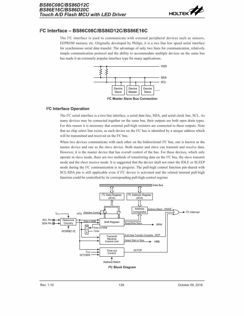
Rev. 1.10 138 October 09, 2018 Rev. 1.10 139 October 09, 2018
BS86C08C/BS86D12CBS86E16C/BS86D20C
Touch A/D Flash MCU with LED Driver
BS86C08C/BS86D12CBS86E16C/BS86D20CTouch A/D Flash MCU with LED Driver
I2C Interface – BS86C08C/BS86D12C/BS86E16CThe I2C interface is used to communicate with external peripheral devices such as sensors, EEPROM memory etc. Originally developed by Philips, it is a two line low speed serial interface for synchronous serial data transfer. The advantage of only two lines for communication, relatively simple communication protocol and the ability to accommodate multiple devices on the same bus has made it an extremely popular interface type for many applications.
Device Slave
Device Master
DeviceSlave
VDD
SDASCL
I2C Master Slave Bus Connection
I2C Interface OperationThe I2C serial interface is a two line interface, a serial data line, SDA, and serial clock line, SCL. As many devices may be connected together on the same bus, their outputs are both open drain types. For this reason it is necessary that external pull-high resistors are connected to these outputs. Note that no chip select line exists, as each device on the I2C bus is identified by a unique address which will be transmitted and received on the I2C bus.
When two devices communicate with each other on the bidirectional I2C bus, one is known as the master device and one as the slave device. Both master and slave can transmit and receive data. However, it is the master device that has overall control of the bus. For these devices, which only operate in slave mode, there are two methods of transferring data on the I2C bus, the slave transmit mode and the slave receive mode. It is suggested that the device shall not enter the IDLE or SLEEP mode during the I2C communication is in progress. The pull-high control function pin-shared with SCL/SDA pin is still applicable even if I2C device is activated and the related internal pull-high function could be controlled by its corresponding pull-high control register.
Shift Register
Transmit/Receive
Control Unit
fSYS
fSUB
Data Bus
I2C Address Register(IICA)
I2C Data Register(IICD)
Address Comparator
Read/Write Slave SRW
Detect Start or Stop HBB
Time-outControl
IICTOF
Address Match - HAASI2C Interrupt
Debounce Circuitry
SCL Pin
MUX TXAK
Data out MSB
IICTOEN
Address Match
IICDEB[1:0]
SDA PinData in MSB
Direction ControlHTX
8-bit Data Transfer Complete - HCF
I2C Block Diagram

Rev. 1.10 140 October 09, 2018 Rev. 1.10 141 October 09, 2018
BS86C08C/BS86D12CBS86E16C/BS86D20C
Touch A/D Flash MCU with LED Driver
BS86C08C/BS86D12CBS86E16C/BS86D20CTouch A/D Flash MCU with LED Driver
START signal from Master
Send slave addressand R/W bit from Master
Acknowledge from slave
Send data byte from Master
Acknowledge from slave
STOP signal from Master
I2C Interface Operation
The IICDEB1 and IICDEB0 bits determine the debounce time of the I2C interface. This uses the internal clock to in effect add a debounce time to the external clock to reduce the possibility of glitches on the clock line causing erroneous operation. The debounce time, if selected, can be chosen to be either 2 or 4 system clocks. To achieve the required I2C data transfer speed, there exists a relationship between the system clock, fSYS, and the I2C debounce time. For either the I2C Standard or Fast mode operation, users must take care of the selected system clock frequency and the configured debounce time to match the criterion shown in the following table.
I2C Debounce Time Selection I2C Standard Mode (100kHz) I2C Fast Mode (400kHz)No Debounce fSYS > 2MHz fSYS > 5MHz2 system clock debounce fSYS > 4MHz fSYS > 10MHz4 system clock debounce fSYS > 8MHz fSYS > 20MHz
I2C Minimum fSYS Frequency Requirements
I2C RegistersThere are three control registers associated with the I2C bus, IICC0, IICC1 and IICTOC, one address register IICA and one data register, IICD.
RegisterName
Bit
7 6 5 4 3 2 1 0IICC0 — — — — IICDEB1 IICDEB0 IICEN —IICC1 HCF HAAS HBB HTX TXAK SRW IAMWU RXAKIICD D7 D6 D5 D4 D3 D2 D1 D0IICA IICA6 IICA5 IICA4 IICA3 IICA2 IICA1 IICA0 —
IICTOC IICTOEN IICTOF IICTOS5 IICTOS4 IICTOS3 IICTOS2 IICTOS1 IICTOS0
I2C Register List
I2C Data RegisterThe IICD register is used to store the data being transmitted and received. Before the device writes data to the I2C bus, the actual data to be transmitted must be placed in the IICD register. After the data is received from the I2C bus, the device can read it from the IICD register. Any transmission or reception of data from the I2C bus must be made via the IICD register.

Rev. 1.10 140 October 09, 2018 Rev. 1.10 141 October 09, 2018
BS86C08C/BS86D12CBS86E16C/BS86D20C
Touch A/D Flash MCU with LED Driver
BS86C08C/BS86D12CBS86E16C/BS86D20CTouch A/D Flash MCU with LED Driver
• IICD Register
Bit 7 6 5 4 3 2 1 0Name D7 D6 D5 D4 D3 D2 D1 D0R/W R/W R/W R/W R/W R/W R/W R/W R/WPOR x x x x x x x x
“x”: unknownBit 7~0 D7~D0: I2C data register bit 7~bit 0
I2C Address RegisterThe IICA register is the location where the 7-bit slave address of the slave device is stored. Bits 7~1 of the IICA register define the device slave address. Bit 0 is not defined. When a master device, which is connected to the I2C bus, sends out an address, which matches the slave address in the IICA register, the slave device will be selected.
• IICA Register
Bit 7 6 5 4 3 2 1 0Name IICA6 IICA5 IICA4 IICA3 IICA2 IICA1 IICA0 —R/W R/W R/W R/W R/W R/W R/W R/W —POR 0 0 0 0 0 0 0 —
Bit 7~1 IICA6~IICA0: I2C slave addressIICA6~IICA0 is the I2C slave address bit 6~bit 0.
Bit 0 Unimplemented, read as “0”
I2C Control RegistersThere are three control registers for the I2C interface, IICC0, IICC1 and IICTOC. The IICC0 register is used to control the enable/disable function and to set the data transmission clock frequency. The IICC1 register contains the relevant flags which are used to indicate the I2C communication status. Another register, IICTOC, is used to control the I2C time-out function and is described in the corresponding section.
• IICC0 Register
Bit 7 6 5 4 3 2 1 0Name — — — — IICDEB1 IICDEB0 IICEN —R/W — — — — R/W R/W R/W —POR — — — — 0 0 0 —
Bit 7~4 Unimplemented, read as “0”Bit 3~2 IICDEB1~IICDEB0: I2C Debounce Time Selection
00: No debounce01: 2 system clock debounce1x: 4 system clock debounce
Note that the I2C debounce circuit will operate normally if the system clock, fSYS, is derived from the fH clock or the IAMWU bit is equal to 0. Otherwise, the debounce circuit will have no effect and be bypassed.
Bit 1 IICEN: I2C Enable Control0: Disable1: Enable
The bit is the overall on/off control for the I2C interface. When the IICEN bit is cleared to zero to disable the I2C interface, the SDA and SCL lines will lose their I2C function and the I2C operating current will be reduced to a minimum value. When the bit is high the I2C interface is enabled. The I2C configuration option must have first enabled

Rev. 1.10 142 October 09, 2018 Rev. 1.10 143 October 09, 2018
BS86C08C/BS86D12CBS86E16C/BS86D20C
Touch A/D Flash MCU with LED Driver
BS86C08C/BS86D12CBS86E16C/BS86D20CTouch A/D Flash MCU with LED Driver
the I2C interface for this bit to be effective. If the IICEN bit changes from low to high, the contents of the I2C control bits such as HTX and TXAK will remain at the previous settings and should therefore be first initialised by the application program while the relevant I2C flags such as HCF, HAAS, HBB, SRW and RXAK will be set to their default states.
Bit 0 Unimplemented, read as “0”
• IICC1 Register
Bit 7 6 5 4 3 2 1 0Name HCF HAAS HBB HTX TXAK SRW IAMWU RXAKR/W R R R R/W R/W R R/W RPOR 1 0 0 0 0 0 0 1
Bit 7 HCF: I2C Bus data transfer completion flag0: Data is being transferred1: Completion of an 8-bit data transfer
The HCF flag is the data transfer flag. This flag will be zero when data is being transferred. Upon completion of an 8-bit data transfer the flag will go high and an interrupt will be generated.
Bit 6 HAAS: I2C Bus address match flag0: Not address match1: Address match
The HAAS flag is the address match flag. This flag is used to determine if the slave device address is the same as the master transmit address. If the addresses match then this bit will be high, if there is no match then the flag will be low.
Bit 5 HBB: I2C Bus busy flag0: I2C Bus is not busy1: I2C Bus is busy
The HBB flag is the I2C busy flag. This flag will be “1” when the I2C bus is busy which will occur when a START signal is detected. The flag will be set to “0” when the bus is free which will occur when a STOP signal is detected.
Bit 4 HTX: I2C slave device is transmitter or receiver selection0: Slave device is the receiver1: Slave device is the transmitter
Bit 3 TXAK: I2C Bus transmit acknowledge flag0: Slave send acknowledge flag1: Slave do not send acknowledge flag
The TXAK bit is the transmit acknowledge flag. After the slave device receipt of 8 bits of data, this bit will be transmitted to the bus on the 9th clock from the slave device. The slave device must always set TXAK bit to “0” before further data is received.
Bit 2 SRW: I2C Slave Read/Write flag0: Slave device should be in receive mode1: Slave device should be in transmit mode
The SRW flag is the I2C Slave Read/Write flag. This flag determines whether the master device wishes to transmit or receive data from the I2C bus. When the transmitted address and slave address is match, that is when the HAAS flag is set high, the slave device will check the SRW flag to determine whether it should be in transmit mode or receive mode. If the SRW flag is high, the master is requesting to read data from the bus, so the slave device should be in transmit mode. When the SRW flag is zero, the master will write data to the bus, therefore the slave device should be in receive mode to read this data.
Bit 1 IAMWU: I2C Address Match Wake-up control0: Disable1: Enable
This bit should be set to 1 to enable the I2C address match wake up from the SLEEP

Rev. 1.10 142 October 09, 2018 Rev. 1.10 143 October 09, 2018
BS86C08C/BS86D12CBS86E16C/BS86D20C
Touch A/D Flash MCU with LED Driver
BS86C08C/BS86D12CBS86E16C/BS86D20CTouch A/D Flash MCU with LED Driver
or IDLE Mode. If the IAMWU bit has been set before entering either the SLEEP or IDLE mode to enable the I2C address match wake up, then this bit must be cleared by the application program after wake-up to ensure correction device operation.
Bit 0 RXAK: I2C Bus Receive acknowledge flag0: Slave receive acknowledge flag1: Slave does not receive acknowledge flag
The RXAK flag is the receiver acknowledge flag. When the RXAK flag is “0”, it means that a acknowledge signal has been received at the 9th clock, after 8 bits of data have been transmitted. When the slave device in the transmit mode, the slave device checks the RXAK flag to determine if the master receiver wishes to receive the next byte. The slave transmitter will therefore continue sending out data until the RXAK flag is “1”. When this occurs, the slave transmitter will release the SDA line to allow the master to send a STOP signal to release the I2C Bus.
I2C Bus CommunicationCommunication on the I2C bus requires four separate steps, a START signal, a slave device address transmission, a data transmission and finally a STOP signal. When a START signal is placed on the I2C bus, all devices on the bus will receive this signal and be notified of the imminent arrival of data on the bus. The first seven bits of the data will be the slave address with the first bit being the MSB. If the address of the slave device matches that of the transmitted address, the HAAS bit in the IICC1 register will be set and an I2C interrupt will be generated. After entering the interrupt service routine, the slave device must first check the condition of the HAAS and IICTOF bits to determine whether the interrupt source originates from an address match or from the completion of an 8-bit data transfer completion or from the I2C bus time-out occurrence. During a data transfer, note that after the 7-bit slave address has been transmitted, the following bit, which is the 8th bit, is the read/write bit whose value will be placed in the SRW bit. This bit will be checked by the slave device to determine whether to go into transmit or receive mode. Before any transfer of data to or from the I2C bus, the microcontroller must initialise the bus, the following are steps to achieve this:
• Step 1Set the IICEN bit in the IICC0 register to “1” to enable the I2C bus.
• Step 2Write the slave address of the device to the I2C bus address register IICA.
• Step 3Set the IICE interrupt enable bit of the interrupt control register to enable the I2C interrupt.

Rev. 1.10 144 October 09, 2018 Rev. 1.10 145 October 09, 2018
BS86C08C/BS86D12CBS86E16C/BS86D20C
Touch A/D Flash MCU with LED Driver
BS86C08C/BS86D12CBS86E16C/BS86D20CTouch A/D Flash MCU with LED Driver
Set IICEN
Write Slave Address to IICA
I2C BusInterrupt=?
CLR IICEPoll IICF to decide
when to go to I2C Bus ISR
No Yes
SET IICEWait for Interrupt
Go to Main Program Go to Main Program
Start
Configure the pin-shared I/O ports to I2C function
I2C Bus Initialisation Flowchart
I2C Bus Start SignalThe START signal can only be generated by the master device connected to the I2C bus and not by the slave device. This START signal will be detected by all devices connected to the I2C bus. When detected, this indicates that the I2C bus is busy and therefore the HBB bit will be set. A START condition occurs when a high to low transition on the SDA line takes place when the SCL line remains high.
I2C Slave AddressThe transmission of a START signal by the master will be detected by all devices on the I2C bus. To determine which slave device the master wishes to communicate with, the address of the slave device will be sent out immediately following the START signal. All slave devices, after receiving this 7-bit address data, will compare it with their own 7-bit slave address. If the address sent out by the master matches the internal address of the microcontroller slave device, then an internal I2C bus interrupt signal will be generated. The next bit following the address, which is the 8th bit, defines the read/write status and will be saved to the SRW bit of the IICC1 register. The slave device will then transmit an acknowledge bit, which is a low level, as the 9th bit. The slave device will also set the status flag HAAS when the addresses match.
As an I2C bus interrupt can come from three sources, when the program enters the interrupt subroutine, the HAAS and IICTOF bits should be examined to see whether the interrupt source has come from a matching slave address or from the completion of a data byte transfer or from the I2C bus time-out occurrence. When a slave address is matched, the device must be placed in either the transmit mode and then write data to the IICD register, or in the receive mode where it must implement a dummy read from the IICD register to release the SCL line.
I2C Bus Read/Write SignalThe SRW bit in the IICC1 register defines whether the master device wishes to read data from the I2C bus or write data to the I2C bus. The slave device should examine this bit to determine if it is to be a transmitter or a receiver. If the SRW flag is “1” then this indicates that the master device wishes to read data from the I2C bus, therefore the slave device must be setup to send data to the I2C bus as

Rev. 1.10 144 October 09, 2018 Rev. 1.10 145 October 09, 2018
BS86C08C/BS86D12CBS86E16C/BS86D20C
Touch A/D Flash MCU with LED Driver
BS86C08C/BS86D12CBS86E16C/BS86D20CTouch A/D Flash MCU with LED Driver
a transmitter. If the SRW flag is “0” then this indicates that the master wishes to send data to the I2C bus, therefore the slave device must be setup to read data from the I2C bus as a receiver.
I2C Bus Slave Address Acknowledge SignalAfter the master has transmitted a calling address, any slave device on the I2C bus, whose own internal address matches the calling address, must generate an acknowledge signal. The acknowledge signal will inform the master that a slave device has accepted its calling address. If no acknowledge signal is received by the master then a STOP signal must be transmitted by the master to end the communication. When the HAAS flag is high, the addresses have matched and the slave device must check the SRW flag to determine if it is to be a transmitter or a receiver. If the SRW flag is high, the slave device should be setup to be a transmitter so the HTX bit in the IICC1 register should be set to “1”. If the SRW flag is low, then the microcontroller slave device should be setup as a receiver and the HTX bit in the IICC1 register should be set to “0”.
I2C Bus Data and Acknowledge SignalThe transmitted data is 8-bit wide and is transmitted after the slave device has acknowledged receipt of its slave address. The order of serial bit transmission is the MSB first and the LSB last. After receipt of 8 bits of data, the receiver must transmit an acknowledge signal, level “0”, before it can receive the next data byte. If the slave transmitter does not receive an acknowledge bit signal from the master receiver, then the slave transmitter will release the SDA line to allow the master to send a STOP signal to release the I2C Bus. The corresponding data will be stored in the IICD register. If setup as a transmitter, the slave device must first write the data to be transmitted into the IICD register. If setup as a receiver, the slave device must read the transmitted data from the IICD register.
When the slave receiver receives the data byte, it must generate an acknowledge bit, known as TXAK, on the 9th clock. The slave device, which is setup as a transmitter will check the RXAK bit in the IICC1 register to determine if it is to send another data byte, if not then it will release the SDA line and await the receipt of a STOP signal from the master.
StartSCL
SDA
SCL
SDA
1
S=Start (1 bit)SA=Slave Address (7 bits)SR=SRW bit (1 bit)M=Slave device send acknowledge bit (1 bit)D=Data (8 bits)A=ACK (RXAK bit for transmitter, TXAK bit for receiver, 1 bit)P=Stop (1 bit)
0
ACKSlave Address SRW
StopData ACK
1 1 0 1 0 1 0
1 0 0 1 0 1 0 0
S SA SR M D A D A …… S SA SR M D A D A …… P
I2C Communication Timing Diagram
Note: When a slave address is matched, the device must be placed in either the transmit mode and then write data to the IICD register, or in the receive mode where it must implement a dummy read from the IICD register to release the SCL line.

Rev. 1.10 146 October 09, 2018 Rev. 1.10 147 October 09, 2018
BS86C08C/BS86D12CBS86E16C/BS86D20C
Touch A/D Flash MCU with LED Driver
BS86C08C/BS86D12CBS86E16C/BS86D20CTouch A/D Flash MCU with LED Driver
Start
IICTOF=1?
SET IICTOENCLR IICTOF
RETI
HAAS=1?
HTX=1? SRW=1?
Read from IICD to release SCL Line
RETI
RXAK=1?
Write data to IICD to release SCL Line
CLR HTXCLR TXAK
Dummy read from IICD to release SCL Line RETI
RETI
SET HTX
Write data to IICD to release SCL Line
RETI
CLR HTXCLR TXAK
Dummy read from IICD to release SCL Line
RETI
YesNo
No Yes
Yes NoYesNo
No
Yes
I2C Bus ISR Flowchart
I2C Time-out ControlIn order to reduce the problem of I2C lockup due to reception of erroneous clock sources, a time-out function is provided. If the clock source to the I2C is not received for a while, then the I2C circuitry and registers will be reset after a certain time-out period. The time-out counter starts counting on an I2C bus “START” & “address match” condition, and is cleared by an SCL falling edge. Before the next SCL falling edge arrives, if the time elapsed is greater than the time-out setup by the IICTOC register, then a time-out condition will occur. The time-out function will stop when an I2C “STOP” condition occurs.
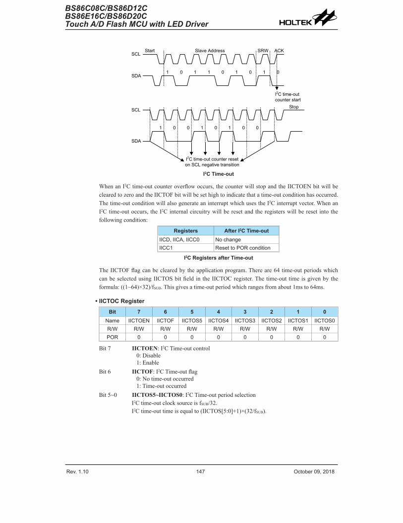
Rev. 1.10 146 October 09, 2018 Rev. 1.10 147 October 09, 2018
BS86C08C/BS86D12CBS86E16C/BS86D20C
Touch A/D Flash MCU with LED Driver
BS86C08C/BS86D12CBS86E16C/BS86D20CTouch A/D Flash MCU with LED Driver
StartSCL
SDA
SCL
SDA
1 0
ACKSlave Address SRW
Stop
1 1 0 1 0 1 0
1 0 0 1 0 1 0 0
I2C time-out counter start
I2C time-out counter reset on SCL negative transition
I2C Time-out
When an I2C time-out counter overflow occurs, the counter will stop and the IICTOEN bit will be cleared to zero and the IICTOF bit will be set high to indicate that a time-out condition has occurred. The time-out condition will also generate an interrupt which uses the I2C interrupt vector. When an I2C time-out occurs, the I2C internal circuitry will be reset and the registers will be reset into the following condition:
Registers After I2C Time-outIICD, IICA, IICC0 No changeIICC1 Reset to POR condition
I2C Registers after Time-out
The IICTOF flag can be cleared by the application program. There are 64 time-out periods which can be selected using IICTOS bit field in the IICTOC register. The time-out time is given by the formula: ((1~64)×32)/fSUB. This gives a time-out period which ranges from about 1ms to 64ms.
• IICTOC Register
Bit 7 6 5 4 3 2 1 0Name IICTOEN IICTOF IICTOS5 IICTOS4 IICTOS3 IICTOS2 IICTOS1 IICTOS0R/W R/W R/W R/W R/W R/W R/W R/W R/WPOR 0 0 0 0 0 0 0 0
Bit 7 IICTOEN: I2C Time-out control0: Disable1: Enable
Bit 6 IICTOF: I2C Time-out flag0: No time-out occurred1: Time-out occurred
Bit 5~0 IICTOS5~IICTOS0: I2C Time-out period selectionI2C time-out clock source is fSUB/32.I2C time-out time is equal to (IICTOS[5:0]+1)×(32/fSUB).

Rev. 1.10 148 October 09, 2018 Rev. 1.10 149 October 09, 2018
BS86C08C/BS86D12CBS86E16C/BS86D20C
Touch A/D Flash MCU with LED Driver
BS86C08C/BS86D12CBS86E16C/BS86D20CTouch A/D Flash MCU with LED Driver
Serial Interface Module – SIM – BS86D20CThe BS86D20C device contains a Serial Interface Module, which includes both the four line SPI interface and the two line I2C interface types, to allow an easy method of communication with external peripheral hardware. Having relatively simple communication protocols, these serial interface types allow the microcontroller to interface to external SPI or I2C based hardware such as sensors, Flash or EEPROM memory, etc. The SIM interface pins are pin-shared with other I/O pins therefore the SIM interface function must first be selected using the SIMEN bit in the SIMC0 register. As both interface types share the same pins and registers, the choice of whether the SPI or I2C type is used is made using the SIM operating mode control bits, named SIM2~SIM0, in the SIMC0 register. These pull-high resistors of the SIM pin-shared I/O are selected using pull-high control registers when the SIM function is enabled and the corresponding pins are used as SIM input pins.
SPI InterfaceThe SPI interface is often used to communicate with external peripheral devices such as sensors, Flash or EEPROM memory devices etc. Originally developed by Motorola, the four line SPI interface is a synchronous serial data interface that has a relatively simple communication protocol simplifying the programming requirements when communicating with external hardware devices.
The communication is full duplex and operates as a slave/master type, where the device can be either master or slave. Although the SPI interface specification can control multiple slave devices from a single master, but the device provides only one SCS pin. If the master needs to control multiple slave devices from a single master, the master can use I/O pin to select the slave devices.
SPI Interface OperationThe SPI interface is a full duplex synchronous serial data link. It is a four line interface with pin names SDI, SDO, SCK and SCS. Pins SDI and SDO are the Serial Data Input and Serial Data Output lines, the SCK pin is the Serial Clock line and SCS is the Slave Select line. As the SPI interface pins are pin-shared with normal I/O pins and with the I2C function pins, the SPI interface pins must first be selected by setting the correct bits in the SIMC0 and SIMC2 registers. Communication between devices connected to the SPI interface is carried out in a slave/master mode with all data transfer initiations being implemented by the master. The Master also controls the clock signal. As the device only contains a single SCS pin only one slave device can be utilized. The SCS pin is controlled by software, set CSEN bit to 1 to enable SCS pin function, set CSEN bit to 0 the SCS pin will be floating state.
SCK
SPI Master
SDO
SDI
SCS
SCK
SPI Slave
SDI
SDO
SCS
SPI Master/Slave Connection

Rev. 1.10 148 October 09, 2018 Rev. 1.10 149 October 09, 2018
BS86C08C/BS86D12CBS86E16C/BS86D20C
Touch A/D Flash MCU with LED Driver
BS86C08C/BS86D12CBS86E16C/BS86D20CTouch A/D Flash MCU with LED Driver
The SPI function in the device offers the following features:
• Full duplex synchronous data transfer
• Both Master and Slave modes
• LSB first or MSB first data transmission modes
• Transmission complete flag
• Rising or falling active clock edge
The status of the SPI interface pins is determined by a number of factors such as whether the device is in the master or slave mode and upon the condition of certain control bits such as CSEN and SIMEN.
SIMD
TX/RX Shift RegisterSDI Pin
Clock Edge/Polarity
Control
CKEG
CKPOLB
ClockSourceSelect
fSYSfSUB
PTM0 CCRP match frequency/2
SCK Pin
CSEN
Busy Status
SDO Pin
SCS Pin
Data Bus
WCOLTRFSIMICF
SPI Block Diagram
SPI RegistersThere are three internal registers which control the overall operation of the SPI interface. These are the SIMD data register and two control registers, SIMC0 and SIMC2.
RegisterName
Bit
7 6 5 4 3 2 1 0SIMC0 SIM2 SIM1 SIM0 — SIMDEB1 SIMDEB0 SIMEN SIMICFSIMC2 D7 D6 CKPOLB CKEG MLS CSEN WCOL TRFSIMD D7 D6 D5 D4 D3 D2 D1 D0
SPI Register List
SPI Data RegisterThe SIMD register is used to store the data being transmitted and received. The same register is used by both the SPI and I2C functions. Before the device writes data to the SPI bus, the actual data to be transmitted must be placed in the SIMD register. After the data is received from the SPI bus, the device can read it from the SIMD register. Any transmission or reception of data from the SPI bus must be made via the SIMD register.
Rev. 1.10 150 October 09, 2018 Rev. 1.10 151 October 09, 2018
BS86C08C/BS86D12CBS86E16C/BS86D20C
Touch A/D Flash MCU with LED Driver
BS86C08C/BS86D12CBS86E16C/BS86D20CTouch A/D Flash MCU with LED Driver
• SIMD Register
Bit 7 6 5 4 3 2 1 0Name D7 D6 D5 D4 D3 D2 D1 D0R/W R/W R/W R/W R/W R/W R/W R/W R/WPOR x x x x x x x x
“x”: unknownBit 7~0 D7~D0: SIM data register bit 7 ~ bit 0
SPI Control RegistersThere are also two control registers for the SPI interface, SIMC0 and SIMC2. Note that the SIMC2 register also has the name SIMA which is used by the I2C function. The SIMC0 register is used to control the enable/disable function and to set the data transmission clock frequency. The SIMC2 register is used for other control functions such as LSB/MSB selection, write collision flag etc.
• SIMC0 Register
Bit 7 6 5 4 3 2 1 0Name SIM2 SIM1 SIM0 — SIMDEB1 SIMDEB0 SIMEN SIMICFR/W R/W R/W R/W — R/W R/W R/W R/WPOR 1 1 1 — 0 0 0 0
Bit 7~5 SIM2~SIM0: SIM Operating Mode Control000: SPI master mode; SPI clock is fSYS/4001: SPI master mode; SPI clock is fSYS/16010: SPI master mode; SPI clock is fSYS/64011: SPI master mode; SPI clock is fSUB
100: SPI master mode; SPI clock is PTM0 CCRP match frequency/2101: SPI slave mode110: I2C slave mode111: Unused mode
These bits setup the overall operating mode of the SIM function. As well as selecting if the I2C or SPI function, they are used to control the SPI Master/Slave selection and the SPI Master clock frequency. The SPI clock is a function of the system clock but can also be chosen to be sourced from PTM0 and fSUB. If the SPI Slave Mode is selected then the clock will be supplied by an external Master device.
Bit 4 Unimplemented, read as “0”Bit 3~2 SIMDEB1~SIMDEB0: I2C Debounce Time Selection
These bits are only available when the SIM is configured to operate in the I2C mode. Refer to the I2C register section.
Bit 1 SIMEN: SIM Enable Control0: Disable1: Enable
The bit is the overall on/off control for the SIM interface. When the SIMEN bit is cleared to zero to disable the SIM interface, the SDI, SDO, SCK and SCS, or SDA and SCL lines will lose their SPI or I2C function and the SIM operating current will be reduced to a minimum value. When the bit is high the SIM interface is enabled. If the SIM is configured to operate as an SPI interface via the SIM2~SIM0 bits, the contents of the SPI control registers will remain at the previous settings when the SIMEN bit changes from low to high and should therefore be first initialised by the application program. If the SIM is configured to operate as an I2C interface via the SIM2~SIM0 bits and the SIMEN bit changes from low to high, the contents of the I2C control bits such as HTX and TXAK will remain at the previous settings and should therefore be first initialised by the application program while the relevant I2C flags such as HCF, HAAS, HBB, SRW and RXAK will be set to their default states.

Rev. 1.10 150 October 09, 2018 Rev. 1.10 151 October 09, 2018
BS86C08C/BS86D12CBS86E16C/BS86D20C
Touch A/D Flash MCU with LED Driver
BS86C08C/BS86D12CBS86E16C/BS86D20CTouch A/D Flash MCU with LED Driver
Bit 0 SIMICF: SIM SPI Incomplete Flag0: SIM SPI incomplete condition is not occurred1: SIM SPI incomplete condition is occurred
This bit is only available when the SIM is configured to operate in an SPI slave mode. If the SPI operates in the slave mode with the SIMEN and CSEN bits both being set to 1 but the SCS line is pulled high by the external master device before the SPI data transfer is completely finished, the SIMICF bit will be set to 1 together with the TRF bit. When this condition occurs, the corresponding interrupt will occur if the interrupt function is enabled. However, the TRF bit will not be set to 1 if the SIMICF bit is set to 1 by software application program.
• SIMC2 Register
Bit 7 6 5 4 3 2 1 0Name D7 D6 CKPOLB CKEG MLS CSEN WCOL TRFR/W R/W R/W R/W R/W R/W R/W R/W R/WPOR 0 0 0 0 0 0 0 0
Bit 7~6 D7~D6: Undefined bitsThese bits can be read or written by the application program.
Bit 5 CKPOLB: SPI clock line base condition selection0: The SCK line will be high when the clock is inactive1: The SCK line will be low when the clock is inactive
The CKPOLB bit determines the base condition of the clock line, if the bit is high, then the SCK line will be low when the clock is inactive. When the CKPOLB bit is low, then the SCK line will be high when the clock is inactive.
Bit 4 CKEG: SPI SCK clock active edge type selectionCKPOLB=0
0: SCK is high base level and data capture at SCK rising edge1: SCK is high base level and data capture at SCK falling edge
CKPOLB=10: SCK is low base level and data capture at SCK falling edge1: SCK is low base level and data capture at SCK rising edge
The CKEG and CKPOLB bits are used to setup the way that the clock signal outputs and inputs data on the SPI bus. These two bits must be configured before data transfer is executed otherwise an erroneous clock edge may be generated. The CKPOLB bit determines the base condition of the clock line, if the bit is high, then the SCK line will be low when the clock is inactive. When the CKPOLB bit is low, then the SCK line will be high when the clock is inactive. The CKEG bit determines active clock edge type which depends upon the condition of CKPOLB bit.
Bit 3 MLS: SPI data shift order0: LSB first1: MSB first
This is the data shift select bit and is used to select how the data is transferred, either MSB or LSB first. Setting the bit high will select MSB first and low for LSB first.
Bit 2 CSEN: SPI SCS pin control0: Disable1: Enable
The CSEN bit is used as an enable/disable for the SCS pin. If this bit is low, then the SCS pin will be disabled and placed into a floating condition. If the bit is high the SCS pin will be enabled and used as a select pin.
Bit 1 WCOL: SPI write collision flag0: No collision1: Collision
The WCOL flag is used to detect if a data collision has occurred. If this bit is high it
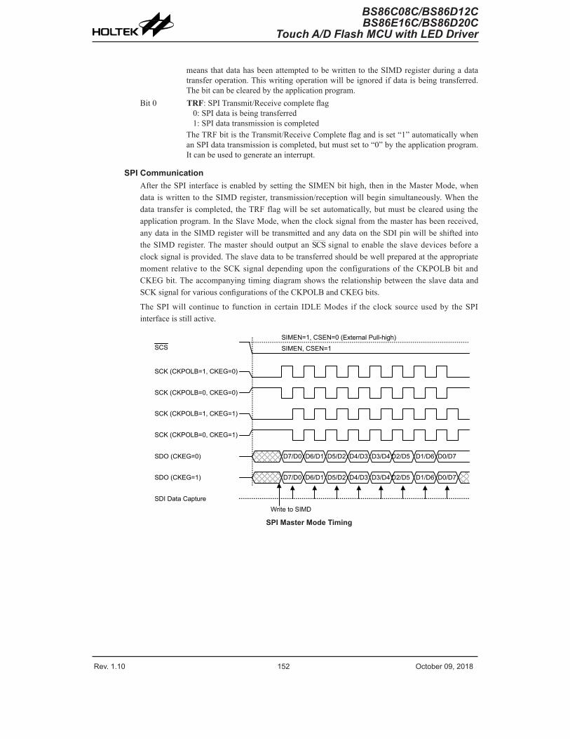
Rev. 1.10 152 October 09, 2018 Rev. 1.10 153 October 09, 2018
BS86C08C/BS86D12CBS86E16C/BS86D20C
Touch A/D Flash MCU with LED Driver
BS86C08C/BS86D12CBS86E16C/BS86D20CTouch A/D Flash MCU with LED Driver
means that data has been attempted to be written to the SIMD register during a data transfer operation. This writing operation will be ignored if data is being transferred. The bit can be cleared by the application program.
Bit 0 TRF: SPI Transmit/Receive complete flag0: SPI data is being transferred1: SPI data transmission is completed
The TRF bit is the Transmit/Receive Complete flag and is set “1” automatically when an SPI data transmission is completed, but must set to “0” by the application program. It can be used to generate an interrupt.
SPI CommunicationAfter the SPI interface is enabled by setting the SIMEN bit high, then in the Master Mode, when data is written to the SIMD register, transmission/reception will begin simultaneously. When the data transfer is completed, the TRF flag will be set automatically, but must be cleared using the application program. In the Slave Mode, when the clock signal from the master has been received, any data in the SIMD register will be transmitted and any data on the SDI pin will be shifted into the SIMD register. The master should output an SCS signal to enable the slave devices before a clock signal is provided. The slave data to be transferred should be well prepared at the appropriate moment relative to the SCK signal depending upon the configurations of the CKPOLB bit and CKEG bit. The accompanying timing diagram shows the relationship between the slave data and SCK signal for various configurations of the CKPOLB and CKEG bits.
The SPI will continue to function in certain IDLE Modes if the clock source used by the SPI interface is still active.
SCK (CKPOLB=1, CKEG=0)
SCK (CKPOLB=0, CKEG=0)
SCK (CKPOLB=1, CKEG=1)
SCK (CKPOLB=0, CKEG=1)
SCS
SDO (CKEG=0)
SDO (CKEG=1)
SDI Data CaptureWrite to SIMD
SIMEN, CSEN=1SIMEN=1, CSEN=0 (External Pull-high)
D7/D0 D6/D1 D5/D2 D4/D3 D3/D4 D2/D5 D1/D6 D0/D7
D7/D0 D6/D1 D5/D2 D4/D3 D3/D4 D2/D5 D1/D6 D0/D7
SPI Master Mode Timing

Rev. 1.10 152 October 09, 2018 Rev. 1.10 153 October 09, 2018
BS86C08C/BS86D12CBS86E16C/BS86D20C
Touch A/D Flash MCU with LED Driver
BS86C08C/BS86D12CBS86E16C/BS86D20CTouch A/D Flash MCU with LED Driver
SCK (CKPOLB=1)
SCK (CKPOLB=0)
SCS
SDO
SDI Data Capture
Write to SIMD(SDO does not change until first SCK edge)
D7/D0 D6/D1 D5/D2 D4/D3 D3/D4 D2/D5 D1/D6 D0/D7
SPI Slave Mode Timing – CKEG=0
SCK (CKPOLB=1)
SCK (CKPOLB=0)
SCS
SDO
SDI Data Capture
D7/D0 D6/D1 D5/D2 D4/D3 D3/D4 D2/D5 D1/D6 D0/D7
Write to SIMD(SDO changes as soon as writing occurs; SDO is floating if SCS=1)
Note: For SPI slave mode, if SIMEN=1 and CSEN=0, SPI is always enabled and ignores the SCS level.
SPI Slave Mode Timing – CKEG=1

Rev. 1.10 154 October 09, 2018 Rev. 1.10 155 October 09, 2018
BS86C08C/BS86D12CBS86E16C/BS86D20C
Touch A/D Flash MCU with LED Driver
BS86C08C/BS86D12CBS86E16C/BS86D20CTouch A/D Flash MCU with LED Driver
Clear WCOL Write Data into SIMD
WCOL=1?
Transmission completed?(TRF=1?)
Read Data from SIMD
Clear TRF
END
Transfer finished?
ASPI Transfer
Master or Slave?
SIMEN=1
Configure CKPOLB, CKEG, CSEN and MLS
A
SIM[2:0]=000, 001, 010, 011 or 100 SIM[2:0]=101
Master Slave
Y
Y
N
N
N
Y
SPI Transfer Control Flowchart

Rev. 1.10 154 October 09, 2018 Rev. 1.10 155 October 09, 2018
BS86C08C/BS86D12CBS86E16C/BS86D20C
Touch A/D Flash MCU with LED Driver
BS86C08C/BS86D12CBS86E16C/BS86D20CTouch A/D Flash MCU with LED Driver
SPI Bus Enable/DisableTo enable the SPI bus, set CSEN=1 and SCS=0, then wait for data to be written into the SIMD (TXRX buffer) register. For the Master Mode, after data has been written to the SIMD (TXRX buffer) register, then transmission or reception will start automatically. When all the data has been transferred, the TRF bit should be set. For the Slave Mode, when clock pulses are received on SCK, data in the TXRX buffer will be shifted out or data on SDI will be shifted in.
When the SPI bus is disabled, SCK, SDI, SDO and SCS can become I/O pins or other pin-shared functions using the corresponding control bits.
SPI Operation StepsAll communication is carried out using the 4-line interface for either Master or Slave Mode.
The CSEN bit in the SIMC2 register controls the overall function of the SPI interface. Setting this bit high will enable the SPI interface by allowing the SCS line to be active, which can then be used to control the SPI interface. If the CSEN bit is low, the SPI interface will be disabled and the SCS line will be in a floating condition and can therefore not be used for control of the SPI interface. If the CSEN bit and the SIMEN bit in the SIMC0 are set high, this will place the SDI line in a floating condition and the SDO line high. If in Master Mode the SCK line will be either high or low depending upon the clock polarity selection bit CKPOLB in the SIMC2 register. If in Slave Mode the SCK line will be in a floating condition. If the SIMEN bit is low, then the bus will be disabled and SCS, SDI, SDO and SCK will all become I/O pins or the other functions using the corresponding control bits. In the Master Mode the Master will always generate the clock signal. The clock and data transmission will be initiated after data has been written into the SIMD register. In the Slave Mode, the clock signal will be received from an external master device for both data transmission and reception. The following sequences show the order to be followed for data transfer in both Master and Slave Mode.
Master Mode• Step 1
Select the SPI Master mode and clock source using the SIM2~SIM0 bits in the SIMC0 control register.
• Step 2Setup the CSEN bit and setup the MLS bit to choose if the data is MSB or LSB first, this setting must be the same with the Slave devices.
• Step 3Setup the SIMEN bit in the SIMC0 control register to enable the SPI interface.
• Step 4For write operations: write the data to the SIMD register, which will actually place the data into the TXRX buffer. Then use the SCK and SCS lines to output the data. After this, go to step 5.For read operations: the data transferred in on the SDI line will be stored in the TXRX buffer until all the data has been received at which point it will be latched into the SIMD register.
• Step 5Check the WCOL bit if set high then a collision error has occurred so return to step 4. If equal to zero then go to the following step.
• Step 6Check the TRF bit or wait for a SPI serial bus interrupt.
• Step 7Read data from the SIMD register.

Rev. 1.10 156 October 09, 2018 Rev. 1.10 157 October 09, 2018
BS86C08C/BS86D12CBS86E16C/BS86D20C
Touch A/D Flash MCU with LED Driver
BS86C08C/BS86D12CBS86E16C/BS86D20CTouch A/D Flash MCU with LED Driver
• Step 8Clear TRF.
• Step 9Go to step 4.
Slave Mode• Step 1
Select the SPI Slave mode using the SIM2~SIM0 bits in the SIMC0 control register
• Step 2
• Setup the CSEN bit and setup the MLS bit to choose if the data is MSB or LSB first, this setting must be the same with the Master devices.
• Step 3Setup the SIMEN bit in the SIMC0 control register to enable the SPI interface.
• Step 4For write operations: write the data to the SIMD register, which will actually place the data into the TXRX buffer. Then wait for the master clock SCK and SCS signal. After this, go to step 5.For read operations: the data transferred in on the SDI line will be stored in the TXRX buffer until all the data has been received at which point it will be latched into the SIMD register.
• Step 5Check the WCOL bit if set high then a collision error has occurred so return to step 4. If equal to zero then go to the following step.
• Step 6Check the TRF bit or wait for a SPI serial bus interrupt.
• Step 7Read data from the SIMD register.
• Step 8Clear TRF.
• Step 9Go to step 4.
Error DetectionThe WCOL bit in the SIMC2 register is provided to indicate errors during data transfer. The bit is set by the SPI serial Interface but must be cleared by the application program. This bit indicates that a data collision has occurred which happens if a write to the SIMD register takes place during a data transfer operation and will prevent the write operation from continuing.

Rev. 1.10 156 October 09, 2018 Rev. 1.10 157 October 09, 2018
BS86C08C/BS86D12CBS86E16C/BS86D20C
Touch A/D Flash MCU with LED Driver
BS86C08C/BS86D12CBS86E16C/BS86D20CTouch A/D Flash MCU with LED Driver
I2C InterfaceThe I2C interface is used to communicate with external peripheral devices such as sensors, EEPROM memory etc. Originally developed by Philips, it is a two line low speed serial interface for synchronous serial data transfer. The advantage of only two lines for communication, relatively simple communication protocol and the ability to accommodate multiple devices on the same bus has made it an extremely popular interface type for many applications.
Device Slave
Device Master
Device Slave
VDD
SDASCL
I2C Master Slave Bus Connection
I2C Interface OperationThe I2C serial interface is a two line interface, a serial data line, SDA, and serial clock line, SCL. As many devices may be connected together on the same bus, their outputs are both open drain types. For this reason it is necessary that external pull-high resistors are connected to these outputs. Note that no chip select line exists, as each device on the I2C bus is identified by a unique address which will be transmitted and received on the I2C bus.
When two devices communicate with each other on the bidirectional I2C bus, one is known as the master device and one as the slave device. Both master and slave can transmit and receive data, however, it is the master device that has overall control of the bus. For the device, which only operates in slave mode, there are two methods of transferring data on the I2C bus, the slave transmit mode and the slave receive mode. It is suggested that the device shall not enter the IDLE or SLEEP mode during the I2C communication is in progress. The pull-high control function pin-shared with SCL/SDA pin is still applicable even if I2C device is activated and the related internal pull-high function could be controlled by its corresponding pull-high control register.
Shift Register
Transmit/Receive
Control Unit
fSYS
fSUB
Data Bus
I2C Address Register(SIMA)
I2C Data Register(SIMD)
Address Comparator
Read/Write Slave SRW
Detect Start or Stop HBB
Time-outControl
SIMTOF
Address Match–HAASI2C Interrupt
Debounce Circuitry
SCL Pin
MUX TXAK
Data out MSB
SIMTOEN
Address Match
SIMDEB[1:0]
SDA PinData in MSB
Direction ControlHTX
8-bit Data Transfer Complete–HCF
I2C Block Diagram
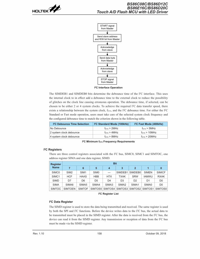
Rev. 1.10 158 October 09, 2018 Rev. 1.10 159 October 09, 2018
BS86C08C/BS86D12CBS86E16C/BS86D20C
Touch A/D Flash MCU with LED Driver
BS86C08C/BS86D12CBS86E16C/BS86D20CTouch A/D Flash MCU with LED Driver
START signal from Master
Send slave addressand R/W bit from Master
Acknowledge from slave
Send data byte from Master
Acknowledge from slave
STOP signal from Master
I2C Interface Operation
The SIMDEB1 and SIMDEB0 bits determine the debounce time of the I2C interface. This uses the internal clock to in effect add a debounce time to the external clock to reduce the possibility of glitches on the clock line causing erroneous operation. The debounce time, if selected, can be chosen to be either 2 or 4 system clocks. To achieve the required I2C data transfer speed, there exists a relationship between the system clock, fSYS, and the I2C debounce time. For either the I2C Standard or Fast mode operation, users must take care of the selected system clock frequency and the configured debounce time to match the criterion shown in the following table.
I2C Debounce Time Selection I2C Standard Mode (100kHz) I2C Fast Mode (400kHz)No Debounce fSYS > 2MHz fSYS > 5MHz2 system clock debounce fSYS > 4MHz fSYS > 10MHz4 system clock debounce fSYS > 8MHz fSYS > 20MHz
I2C Minimum fSYS Frequency Requirements
I2C RegistersThere are three control registers associated with the I2C bus, SIMC0, SIMC1 and SIMTOC, one address register SIMA and one data register, SIMD.
RegisterName
Bit
7 6 5 4 3 2 1 0SIMC0 SIM2 SIM1 SIM0 — SIMDEB1 SIMDEB0 SIMEN SIMICFSIMC1 HCF HAAS HBB HTX TXAK SRW IAMWU RXAKSIMD D7 D6 D5 D4 D3 D2 D1 D0SIMA SIMA6 SIMA5 SIMA4 SIMA3 SIMA2 SIMA1 SIMA0 D0
SIMTOC SIMTOEN SIMTOF SIMTOS5 SIMTOS4 SIMTOS3 SIMTOS2 SIMTOS1 SIMTOS0
I2C Register List
I2C Data RegisterThe SIMD register is used to store the data being transmitted and received. The same register is used by both the SPI and I2C functions. Before the device writes data to the I2C bus, the actual data to be transmitted must be placed in the SIMD register. After the data is received from the I2C bus, the device can read it from the SIMD register. Any transmission or reception of data from the I2C bus must be made via the SIMD register.

Rev. 1.10 158 October 09, 2018 Rev. 1.10 159 October 09, 2018
BS86C08C/BS86D12CBS86E16C/BS86D20C
Touch A/D Flash MCU with LED Driver
BS86C08C/BS86D12CBS86E16C/BS86D20CTouch A/D Flash MCU with LED Driver
• SIMD Register
Bit 7 6 5 4 3 2 1 0Name D7 D6 D5 D4 D3 D2 D1 D0R/W R/W R/W R/W R/W R/W R/W R/W R/WPOR x x x x x x x x
“x”: unknownBit 7~0 D7~D0: SIM data register bit 7 ~ bit 0
I2C Address RegisterThe SIMA register is also used by the SPI interface but has the name SIMC2. The SIMA register is the location where the 7-bit slave address of the slave device is stored. Bits 7~1 of the SIMA register define the device slave address. Bit 0 is not defined. When a master device, which is connected to the I2C bus, sends out an address, which matches the slave address in the SIMA register, the slave device will be selected. Note that the SIMA register is the same register address as SIMC2 which is used by the SPI interface.
• SIMA Register
Bit 7 6 5 4 3 2 1 0Name SIMA6 SIMA5 SIMA4 SIMA3 SIMA2 SIMA1 SIMA0 D0R/W R/W R/W R/W R/W R/W R/W R/W R/WPOR 0 0 0 0 0 0 0 0
Bit 7~1 SIMA6~SIMA0: I2C slave addressSIMA6~SIMA0 is the I2C slave address bit 6~bit 0.
Bit 0 D0: Reserved bit, can be read or written by application program
I2C Control RegistersThere are three control registers for the I2C interface, SIMC0, SIMC1 and SIMTOC. The SIMC0 register is used to control the enable/disable function and to set the data transmission clock frequency. The SIMC1 register contains the relevant flags which are used to indicate the I2C communication status. Another register, SIMTOC, is used to control the I2C time-out function and is described in the corresponding section.
• SIMC0 Register
Bit 7 6 5 4 3 2 1 0Name SIM2 SIM1 SIM0 — SIMDEB1 SIMDEB0 SIMEN SIMICFR/W R/W R/W R/W — R/W R/W R/W R/WPOR 1 1 1 — 0 0 0 0
Bit 7~5 SIM2~SIM0: SIM Operating Mode Control000: SPI master mode; SPI clock is fSYS/4001: SPI master mode; SPI clock is fSYS/16010: SPI master mode; SPI clock is fSYS/64011: SPI master mode; SPI clock is fSUB
100: SPI master mode; SPI clock is PTM0 CCRP match frequency/2101: SPI slave mode110: I2C slave mode111: Unused mode
These bits setup the overall operating mode of the SIM function. As well as selecting if the I2C or SPI function, they are used to control the SPI Master/Slave selection and the SPI Master clock frequency. The SPI clock is a function of the system clock but can also be chosen to be sourced from PTM0 and fSUB. If the SPI Slave Mode is selected

Rev. 1.10 160 October 09, 2018 Rev. 1.10 161 October 09, 2018
BS86C08C/BS86D12CBS86E16C/BS86D20C
Touch A/D Flash MCU with LED Driver
BS86C08C/BS86D12CBS86E16C/BS86D20CTouch A/D Flash MCU with LED Driver
then the clock will be supplied by an external Master device.Bit 4 Unimplemented, read as “0”Bit 3~2 SIMDEB1~SIMDEB0: I2C Debounce Time Selection
00: No debounce01: 2 system clock debounce1x: 4 system clock debounce
These bits are used to select the I2C debounce time when the SIM is configured as the I2C interface function by setting the SIM2~SIM0 bits to “110”.
Bit 1 SIMEN: SIM Enable Control0: Disable1: Enable
The bit is the overall on/off control for the SIM interface. When the SIMEN bit is cleared to zero to disable the SIM interface, the SDI, SDO, SCK and SCS, or SDA and SCL lines will lose their SPI or I2C function and the SIM operating current will be reduced to a minimum value. When the bit is high the SIM interface is enabled. If the SIM is configured to operate as an SPI interface via the SIM2~SIM0 bits, the contents of the SPI control registers will remain at the previous settings when the SIMEN bit changes from low to high and should therefore be first initialised by the application program. If the SIM is configured to operate as an I2C interface via the SIM2~SIM0 bits and the SIMEN bit changes from low to high, the contents of the I2C control bits such as HTX and TXAK will remain at the previous settings and should therefore be first initialised by the application program while the relevant I2C flags such as HCF, HAAS, HBB, SRW and RXAK will be set to their default states.
Bit 0 SIMICF: SIM SPI Incomplete FlagThis bit is only available when the SIM is configured to operate in an SPI slave mode. Refer to the SPI register section.
• SIMC1 Register
Bit 7 6 5 4 3 2 1 0Name HCF HAAS HBB HTX TXAK SRW IAMWU RXAKR/W R R R R/W R/W R R/W RPOR 1 0 0 0 0 0 0 1
Bit 7 HCF: I2C Bus data transfer completion flag0: Data is being transferred1: Completion of an 8-bit data transfer
The HCF flag is the data transfer flag. This flag will be zero when data is being transferred. Upon completion of an 8-bit data transfer the flag will go high and an interrupt will be generated.
Bit 6 HAAS: I2C Bus address match flag0: Not address match1: Address match
The HAAS flag is the address match flag. This flag is used to determine if the slave device address is the same as the master transmit address. If the addresses match then this bit will be high, if there is no match then the flag will be low.
Bit 5 HBB: I2C Bus busy flag0: I2C Bus is not busy1: I2C Bus is busy
The HBB flag is the I2C busy flag. This flag will be “1” when the I2C bus is busy which will occur when a START signal is detected. The flag will be set to “0” when the bus is free which will occur when a STOP signal is detected.
Bit 4 HTX: I2C slave device is transmitter or receiver selection0: Slave device is the receiver1: Slave device is the transmitter
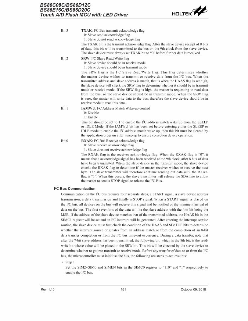
Rev. 1.10 160 October 09, 2018 Rev. 1.10 161 October 09, 2018
BS86C08C/BS86D12CBS86E16C/BS86D20C
Touch A/D Flash MCU with LED Driver
BS86C08C/BS86D12CBS86E16C/BS86D20CTouch A/D Flash MCU with LED Driver
Bit 3 TXAK: I2C Bus transmit acknowledge flag0: Slave send acknowledge flag1: Slave do not send acknowledge flag
The TXAK bit is the transmit acknowledge flag. After the slave device receipt of 8 bits of data, this bit will be transmitted to the bus on the 9th clock from the slave device. The slave device must always set TXAK bit to “0” before further data is received.
Bit 2 SRW: I2C Slave Read/Write flag0: Slave device should be in receive mode1: Slave device should be in transmit mode
The SRW flag is the I2C Slave Read/Write flag. This flag determines whether the master device wishes to transmit or receive data from the I2C bus. When the transmitted address and slave address is match, that is when the HAAS flag is set high, the slave device will check the SRW flag to determine whether it should be in transmit mode or receive mode. If the SRW flag is high, the master is requesting to read data from the bus, so the slave device should be in transmit mode. When the SRW flag is zero, the master will write data to the bus, therefore the slave device should be in receive mode to read this data.
Bit 1 IAMWU: I2C Address Match Wake-up control0: Disable1: Enable
This bit should be set to 1 to enable the I2C address match wake up from the SLEEP or IDLE Mode. If the IAMWU bit has been set before entering either the SLEEP or IDLE mode to enable the I2C address match wake up, then this bit must be cleared by the application program after wake-up to ensure correction device operation.
Bit 0 RXAK: I2C Bus Receive acknowledge flag0: Slave receive acknowledge flag1: Slave does not receive acknowledge flag
The RXAK flag is the receiver acknowledge flag. When the RXAK flag is “0”, it means that a acknowledge signal has been received at the 9th clock, after 8 bits of data have been transmitted. When the slave device in the transmit mode, the slave device checks the RXAK flag to determine if the master receiver wishes to receive the next byte. The slave transmitter will therefore continue sending out data until the RXAK flag is “1”. When this occurs, the slave transmitter will release the SDA line to allow the master to send a STOP signal to release the I2C Bus.
I2C Bus CommunicationCommunication on the I2C bus requires four separate steps, a START signal, a slave device address transmission, a data transmission and finally a STOP signal. When a START signal is placed on the I2C bus, all devices on the bus will receive this signal and be notified of the imminent arrival of data on the bus. The first seven bits of the data will be the slave address with the first bit being the MSB. If the address of the slave device matches that of the transmitted address, the HAAS bit in the SIMC1 register will be set and an I2C interrupt will be generated. After entering the interrupt service routine, the slave device must first check the condition of the HAAS and SIMTOF bits to determine whether the interrupt source originates from an address match or from the completion of an 8-bit data transfer completion or from the I2C bus time-out occurrence. During a data transfer, note that after the 7-bit slave address has been transmitted, the following bit, which is the 8th bit, is the read/write bit whose value will be placed in the SRW bit. This bit will be checked by the slave device to determine whether to go into transmit or receive mode. Before any transfer of data to or from the I2C bus, the microcontroller must initialise the bus, the following are steps to achieve this:
• Step 1Set the SIM2~SIM0 and SIMEN bits in the SIMC0 register to “110” and “1” respectively to enable the I2C bus.

Rev. 1.10 162 October 09, 2018 Rev. 1.10 163 October 09, 2018
BS86C08C/BS86D12CBS86E16C/BS86D20C
Touch A/D Flash MCU with LED Driver
BS86C08C/BS86D12CBS86E16C/BS86D20CTouch A/D Flash MCU with LED Driver
• Step 2Write the slave address of the device to the I2C bus address register SIMA.
• Step 3Set the SIME interrupt enable bit of the interrupt control register to enable the SIM interrupt.
Start
SET SIM[2:0]=110SET SIMEN
Write Slave Address to SIMA
I2C Bus Interrupt=?
CLR SIMEPoll SIMF to decide
when to go to I2C Bus ISR
SET SIMEWait for Interrupt
Go to Main Program Go to Main Program
YesNo
I2C Bus Initialisation Flow Chart
I2C Bus Start SignalThe START signal can only be generated by the master device connected to the I2C bus and not by the slave device. This START signal will be detected by all devices connected to the I2C bus. When detected, this indicates that the I2C bus is busy and therefore the HBB bit will be set. A START condition occurs when a high to low transition on the SDA line takes place when the SCL line remains high.
I2C Slave AddressThe transmission of a START signal by the master will be detected by all devices on the I2C bus. To determine which slave device the master wishes to communicate with, the address of the slave device will be sent out immediately following the START signal. All slave devices, after receiving this 7-bit address data, will compare it with their own 7-bit slave address. If the address sent out by the master matches the internal address of the microcontroller slave device, then an internal I2C bus interrupt signal will be generated. The next bit following the address, which is the 8th bit, defines the read/write status and will be saved to the SRW bit of the SIMC1 register. The slave device will then transmit an acknowledge bit, which is a low level, as the 9th bit. The slave device will also set the status flag HAAS when the addresses match.
As an I2C bus interrupt can come from three sources, when the program enters the interrupt subroutine, the HAAS and SIMTOF bits should be examined to see whether the interrupt source has come from a matching slave address or from the completion of a data byte transfer or from the I2C bus time-out occurrence. When a slave address is matched, the device must be placed in either the transmit mode and then write data to the SIMD register, or in the receive mode where it must implement a dummy read from the SIMD register to release the SCL line.

Rev. 1.10 162 October 09, 2018 Rev. 1.10 163 October 09, 2018
BS86C08C/BS86D12CBS86E16C/BS86D20C
Touch A/D Flash MCU with LED Driver
BS86C08C/BS86D12CBS86E16C/BS86D20CTouch A/D Flash MCU with LED Driver
I2C Bus Read/Write SignalThe SRW bit in the SIMC1 register defines whether the master device wishes to read data from the I2C bus or write data to the I2C bus. The slave device should examine this bit to determine if it is to be a transmitter or a receiver. If the SRW flag is “1” then this indicates that the master device wishes to read data from the I2C bus, therefore the slave device must be setup to send data to the I2C bus as a transmitter. If the SRW flag is “0” then this indicates that the master wishes to send data to the I2C bus, therefore the slave device must be setup to read data from the I2C bus as a receiver.
I2C Bus Slave Address Acknowledge SignalAfter the master has transmitted a calling address, any slave device on the I2C bus, whose own internal address matches the calling address, must generate an acknowledge signal. The acknowledge signal will inform the master that a slave device has accepted its calling address. If no acknowledge signal is received by the master then a STOP signal must be transmitted by the master to end the communication. When the HAAS flag is high, the addresses have matched and the slave device must check the SRW flag to determine if it is to be a transmitter or a receiver. If the SRW flag is high, the slave device should be setup to be a transmitter so the HTX bit in the SIMC1 register should be set to “1”. If the SRW flag is low, then the microcontroller slave device should be setup as a receiver and the HTX bit in the SIMC1 register should be set to “0”.
I2C Bus Data and Acknowledge SignalThe transmitted data is 8-bit wide and is transmitted after the slave device has acknowledged receipt of its slave address. The order of serial bit transmission is the MSB first and the LSB last. After receipt of 8 bits of data, the receiver must transmit an acknowledge signal, level “0”, before it can receive the next data byte. If the slave transmitter does not receive an acknowledge bit signal from the master receiver, then the slave transmitter will release the SDA line to allow the master to send a STOP signal to release the I2C Bus. The corresponding data will be stored in the SIMD register. If setup as a transmitter, the slave device must first write the data to be transmitted into the SIMD register. If setup as a receiver, the slave device must read the transmitted data from the SIMD register.
When the slave receiver receives the data byte, it must generate an acknowledge bit, known as TXAK, on the 9th clock. The slave device, which is setup as a transmitter will check the RXAK bit in the SIMC1 register to determine if it is to send another data byte, if not then it will release the SDA line and await the receipt of a STOP signal from the master.
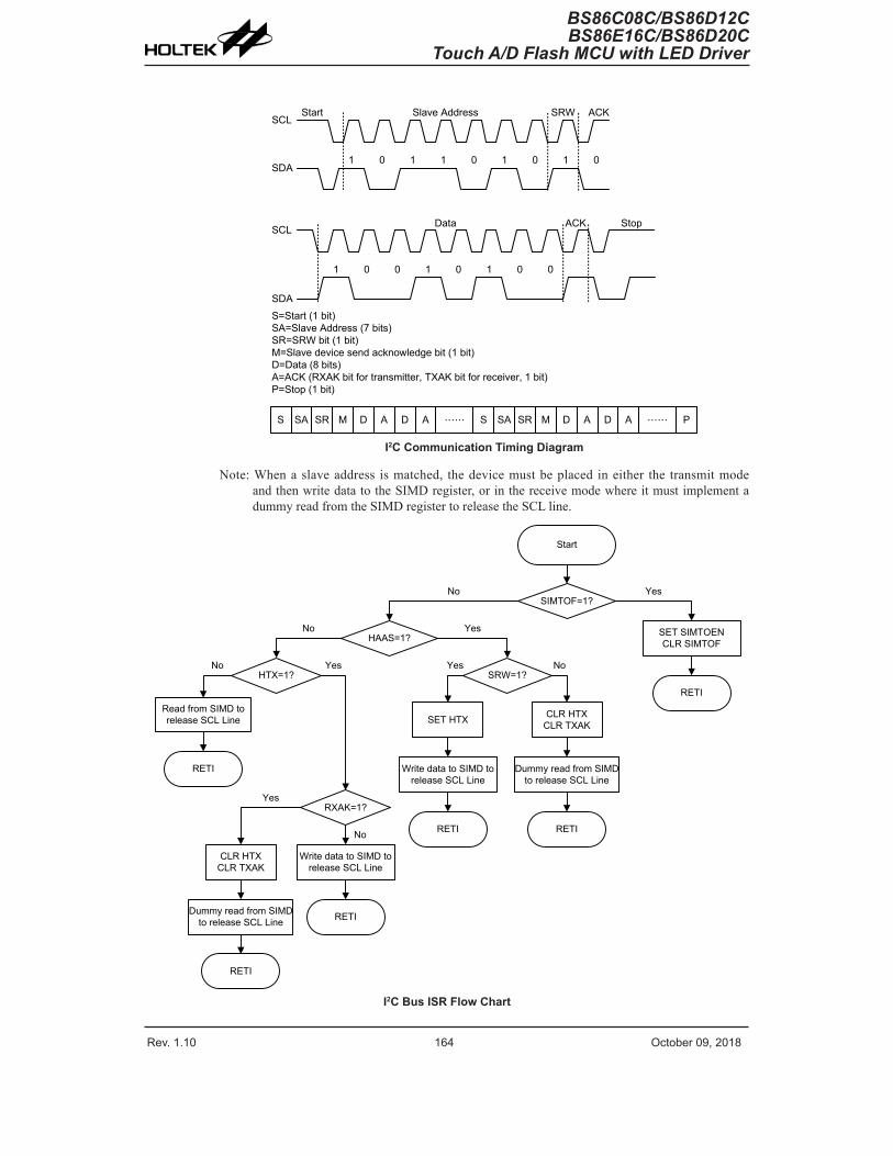
Rev. 1.10 164 October 09, 2018 Rev. 1.10 165 October 09, 2018
BS86C08C/BS86D12CBS86E16C/BS86D20C
Touch A/D Flash MCU with LED Driver
BS86C08C/BS86D12CBS86E16C/BS86D20CTouch A/D Flash MCU with LED Driver
StartSCL
SDA
SCL
SDA
1
S=Start (1 bit)SA=Slave Address (7 bits)SR=SRW bit (1 bit)M=Slave device send acknowledge bit (1 bit)D=Data (8 bits)A=ACK (RXAK bit for transmitter, TXAK bit for receiver, 1 bit)P=Stop (1 bit)
0
ACKSlave Address SRW
StopData ACK
1 1 0 1 0 1 0
1 0 0 1 0 1 0 0
S SA SR M D A D A …… S SA SR M D A D A …… P
I2C Communication Timing Diagram
Note: When a slave address is matched, the device must be placed in either the transmit mode and then write data to the SIMD register, or in the receive mode where it must implement a dummy read from the SIMD register to release the SCL line.
Start
SIMTOF=1?
SET SIMTOENCLR SIMTOF
RETI
HAAS=1?
HTX=1? SRW=1?
Read from SIMD to release SCL Line
RETI
RXAK=1?
Write data to SIMD to release SCL Line
CLR HTXCLR TXAK
Dummy read from SIMD to release SCL Line RETI
RETI
SET HTX
Write data to SIMD to release SCL Line
RETI
CLR HTXCLR TXAK
Dummy read from SIMD to release SCL Line
RETI
YesNo
No Yes
Yes NoYesNo
No
Yes
I2C Bus ISR Flow Chart
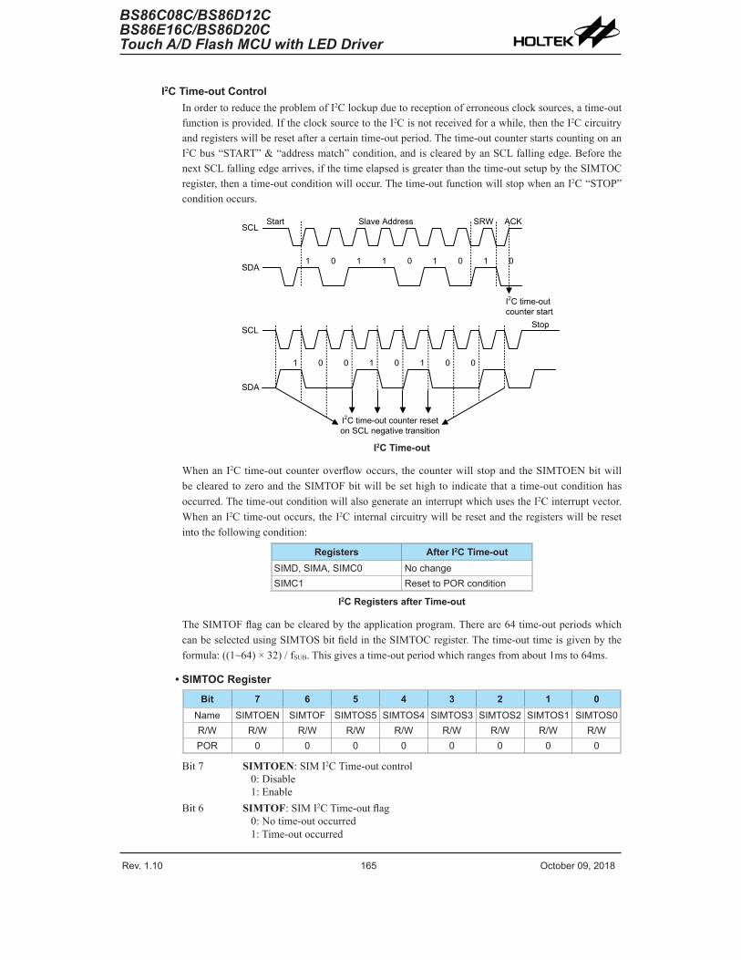
Rev. 1.10 164 October 09, 2018 Rev. 1.10 165 October 09, 2018
BS86C08C/BS86D12CBS86E16C/BS86D20C
Touch A/D Flash MCU with LED Driver
BS86C08C/BS86D12CBS86E16C/BS86D20CTouch A/D Flash MCU with LED Driver
I2C Time-out ControlIn order to reduce the problem of I2C lockup due to reception of erroneous clock sources, a time-out function is provided. If the clock source to the I2C is not received for a while, then the I2C circuitry and registers will be reset after a certain time-out period. The time-out counter starts counting on an I2C bus “START” & “address match” condition, and is cleared by an SCL falling edge. Before the next SCL falling edge arrives, if the time elapsed is greater than the time-out setup by the SIMTOC register, then a time-out condition will occur. The time-out function will stop when an I2C “STOP” condition occurs.
StartSCL
SDA
SCL
SDA
1 0
ACKSlave Address SRW
Stop
1 1 0 1 0 1 0
1 0 0 1 0 1 0 0
I2C time-out counter start
I2C time-out counter reset on SCL negative transition
I2C Time-out
When an I2C time-out counter overflow occurs, the counter will stop and the SIMTOEN bit will be cleared to zero and the SIMTOF bit will be set high to indicate that a time-out condition has occurred. The time-out condition will also generate an interrupt which uses the I2C interrupt vector. When an I2C time-out occurs, the I2C internal circuitry will be reset and the registers will be reset into the following condition:
Registers After I2C Time-outSIMD, SIMA, SIMC0 No changeSIMC1 Reset to POR condition
I2C Registers after Time-out
The SIMTOF flag can be cleared by the application program. There are 64 time-out periods which can be selected using SIMTOS bit field in the SIMTOC register. The time-out time is given by the formula: ((1~64) × 32) / fSUB. This gives a time-out period which ranges from about 1ms to 64ms.
• SIMTOC Register
Bit 7 6 5 4 3 2 1 0Name SIMTOEN SIMTOF SIMTOS5 SIMTOS4 SIMTOS3 SIMTOS2 SIMTOS1 SIMTOS0R/W R/W R/W R/W R/W R/W R/W R/W R/WPOR 0 0 0 0 0 0 0 0
Bit 7 SIMTOEN: SIM I2C Time-out control0: Disable1: Enable
Bit 6 SIMTOF: SIM I2C Time-out flag0: No time-out occurred1: Time-out occurred

Rev. 1.10 166 October 09, 2018 Rev. 1.10 167 October 09, 2018
BS86C08C/BS86D12CBS86E16C/BS86D20C
Touch A/D Flash MCU with LED Driver
BS86C08C/BS86D12CBS86E16C/BS86D20CTouch A/D Flash MCU with LED Driver
Bit 5~0 SIMTOS5~SIMTOS0: SIM I2C Time-out period selectionI2C time-out clock source is fSUB/32.I2C time-out time is equal to (SIMTOS[5:0]+1) × (32/fSUB).
UART InterfacesThese devices contain up to two integrated full-duplex asynchronous serial communications UART interfaces that enable communication with external devices that contain a serial interface. Each UART function has many features and can transmit and receive data serially by transferring a frame of data with eight or nine data bits per transmission as well as being able to detect errors when the data is overwritten or incorrectly framed. Each UART function possesses its own internal interrupt which can be used to indicate when a reception occurs or when a transmission terminates.
Device UARTBS86C08CBS86D12CBS86D20C
UART0
BS86E16C UART0, UART1
The integrated UART functions contain the following features:
• Full-duplex, asynchronous communication
• 8 or 9 bits character length
• Even, odd or no parity options
• One or two stop bits
• Baud rate generator with 8-bit prescaler
• Parity, framing, noise and overrun error detection
• Support for interrupt on address detect (last character bit=1)
• Separately enabled transmitter and receiver
• 2-byte Deep FIFO Receive Data Buffer
• RXn pin wake-up function
• Transmit and receive interrupts
• Interrupts can be initialized by the following conditions: ♦ Transmitter Empty ♦ Transmitter Idle ♦ Receiver Full ♦ Receiver Overrun ♦ Address Mode Detect
MSB LSB…………………………
Transmitter Shift Register (TSRn)MSB LSB…………………………
Receiver Shift Register (RSRn)TXn Pin RXn Pin
Baud Rate Generator
TXR_RXRn Register TXR_RXRn Register
Data to be transmitted Data received
BufferfH
MCU Data Bus
UARTn Data Transfer Block Diagram (n=0~1)

Rev. 1.10 166 October 09, 2018 Rev. 1.10 167 October 09, 2018
BS86C08C/BS86D12CBS86E16C/BS86D20C
Touch A/D Flash MCU with LED Driver
BS86C08C/BS86D12CBS86E16C/BS86D20CTouch A/D Flash MCU with LED Driver
UARTn External PinsTo communicate with an external serial interface, the internal UARTn has two external pins known as TXn and RXn. The TXn and RXn pins are the UART transmitter and receiver pins respectively. Along with the UARTENn bit, the TXENn and RXENn bits, if set, will setup these pins to their respective TXn output and RXn input conditions and disable any pull-high resistor option which may exist on the TXn and RXn pins. However, the RXn pin function should first be selected by the corresponding pin-shared function control bit, RXnEN, in the IFS2 register before the UARTn function is used. When the TXn or RXn pin function is disabled by clearing the UARTENn, TXENn or RXENn bit, the TXn or RXn pin will be placed into a floating state. At this time whether the internal pull-high resistor is connected to the TXn or RXn pin or not is determined by the corresponding I/O pull-high function control bit.
UARTn Data Transfer SchemeThe above block diagram shows the overall data transfer structure arrangement for the UARTn. The actual data to be transmitted from the MCU is first transferred to the TXR_RXRn register by the application program. The data will then be transferred to the Transmit Shift Register from where it will be shifted out, LSB first, onto the TXn pin at a rate controlled by the Baud Rate Generator. Only the TXR_RXRn register is mapped onto the MCU Data Memory, the Transmit Shift Register is not mapped and is therefore inaccessible to the application program.
Data to be received by the UARTn is accepted on the external RXn pin, from where it is shifted in, LSB first, to the Receiver Shift Register at a rate controlled by the Baud Rate Generator. When the shift register is full, the data will then be transferred from the shift register to the internal TXR_RXRn register, where it is buffered and can be manipulated by the application program. Only the TXR_RXRn register is mapped onto the MCU Data Memory, the Receiver Shift Register is not mapped and is therefore inaccessible to the application program.
It should be noted that the actual register for data transmission and reception only exists as a single shared register in the Data Memory. This shared register known as the TXR_RXRn register is used for both data transmission and data reception.
UARTn Status and Control RegistersThere are five control registers associated with the UARTn function. The UnSR, UnCR1 and UnCR2 registers control the overall function of the UARTn, while the BRGn register controls the Baud rate. The actual data to be transmitted and received on the serial interface is managed through the TXR_RXRn data register.
RegisterName
Bit
7 6 5 4 3 2 1 0UnSR PERRn NFn FERRn OERRn RIDLEn RXIFn TIDLEn TXIFn
UnCR1 UARTENn BNOn PRENn PRTn STOPSn TXBRKn RX8n TX8nUnCR2 TXENn RXENn BRGHn ADDENn WAKEn RIEn TIIEn TEIEn
TXR_RXRn TXRXn7 TXRXn6 TXRXn5 TXRXn4 TXRXn3 TXRXn2 TXRXn1 TXRXn0BRGn BRGn7 BRGn6 BRGn5 BRGn4 BRGn3 BRGn2 BRGn1 BRGn0
UARTn Register List (n=0~1)

Rev. 1.10 168 October 09, 2018 Rev. 1.10 169 October 09, 2018
BS86C08C/BS86D12CBS86E16C/BS86D20C
Touch A/D Flash MCU with LED Driver
BS86C08C/BS86D12CBS86E16C/BS86D20CTouch A/D Flash MCU with LED Driver
• UnSR RegisterThe UnSR register is the status register for the UARTn, which can be read by the program to determine the present status of the UARTn. All flags within the UnSR register are read only. Further explanation on each of the flags is given below:
Bit 7 6 5 4 3 2 1 0Name PERRn NFn FERRn OERRn RIDLEn RXIFn TIDLEn TXIFnR/W R R R R R R R RPOR 0 0 0 0 1 0 1 1
Bit 7 PERRn: Parity error flag0: No parity error is detected1: Parity error is detected
The PERRn flag is the parity error flag. When this read only flag is “0”, it indicates a parity error has not been detected. When the flag is “1”, it indicates that the parity of the received word is incorrect. This error flag is applicable only if Parity mode (odd or even) is selected. The flag can also be cleared by a software sequence which involves a read to the status register UnSR followed by an access to the TXR_RXRn data register.
Bit 6 NFn: Noise flag0: No noise is detected1: Noise is detected
The NFn flag is the noise flag. When this read only flag is “0”, it indicates no noise condition. When the flag is “1”, it indicates that the UARTn has detected noise on the receiver input. The NFn flag is set during the same cycle as the RXIFn flag but will not be set in the case of as overrun. The NFn flag can be cleared by a software sequence which will involve a read to the status register UnSR followed by an access to the TXR_RXRn data register.
Bit 5 FERRn: Framing error flag0: No framing error is detected1: Framing error is detected
The FERRn flag is the framing error flag. When this read only flag is “0”, it indicates that there is no framing error. When the flag is “1”, it indicates that a framing error has been detected for the current character. The flag can also be cleared by a software sequence which will involve a read to the status register UnSR followed by an access to the TXR_RXRn data register.
Bit 4 OERRn: Overrun error flag0: No overrun error is detected1: Overrun error is detected
The OERRn flag is the overrun error flag which indicates when the receiver buffer has overflowed. When this read only flag is “0”, it indicates that there is no overrun error. When the flag is “1”, it indicates that an overrun error occurs which will inhibit further transfers to the TXR_RXRn receive data register. The flag is cleared by a software sequence, which is a read to the status register UnSR followed by an access to the TXR_RXRn data register.
Bit 3 RIDLEn: Receiver status0: Data reception is in progress (Data being received)1: No data reception is in progress (Receiver is idle)
The RIDLEn flag is the receiver status flag. When this read only flag is “0”, it indicates that the receiver is between the initial detection of the start bit and the completion of the stop bit. When the flag is “1”, it indicates that the receiver is idle. Between the completion of the stop bit and the detection of the next start bit, the RIDLEn bit is “1” indicating that the UARTn receiver is idle and the RXn pin stays in logic high condition.

Rev. 1.10 168 October 09, 2018 Rev. 1.10 169 October 09, 2018
BS86C08C/BS86D12CBS86E16C/BS86D20C
Touch A/D Flash MCU with LED Driver
BS86C08C/BS86D12CBS86E16C/BS86D20CTouch A/D Flash MCU with LED Driver
Bit 2 RXIFn: Receive TXR_RXRn data register status0: TXR_RXRn data register is empty1: TXR_RXRn data register has available data
The RXIFn flag is the receive data register status flag. When this read only flag is “0”, it indicates that the TXR_RXRn read data register is empty. When the flag is “1”, it indicates that the TXR_RXRn read data register contains new data. When the contents of the shift register are transferred to the TXR_RXRn register, an interrupt is generated if RIEn=1 in the UnCR2 register. If one or more errors are detected in the received word, the appropriate receive-related flags NFn, FERRn, and/or PERRn are set within the same clock cycle. The RXIFn flag will eventually be cleared when the UnSR register is read with RXIFn set, followed by a read from the TXR_RXR register, and if the TXR_RXR register has no more new data available.
Bit 1 TIDLEn: Transmission idle0: Data transmission is in progress (Data being transmitted)1: No data transmission is in progress (Transmitter is idle)
The TIDLEn flag is known as the transmission complete flag. When this read only flag is “0”, it indicates that a transmission is in progress. This flag will be set high when the TXIFn flag is “1” and when there is no transmit data or break character being transmitted. When TIDLEn is equal to “1”, the TXn pin becomes idle with the pin state in logic high condition. The TIDLEn flag is cleared by reading the UnSR register with TIDLEn set and then writing to the TXR_RXRn register. The flag is not generated when a data character or a break is queued and ready to be sent.
Bit 0 TXIFn: Transmit TXR_RXRn data register status0: Character is not transferred to the transmit shift register1: Character has transferred to the transmit shift register (TXR_RXRn data register
is empty)The TXIFn flag is the transmit data register empty flag. When this read only flag is “0”, it indicates that the character is not transferred to the transmitter shift register. When the flag is “1”, it indicates that the transmitter shift register has received a character from the TXR_RXRn data register. The TXIFn flag is cleared by reading the UARTn status register (UnSR) with TXIFn set and then writing to the TXR_RXRn data register. Note that when the TXENn bit is set, the TXIFn flag bit will also be set since the transmit data register is not yet full.
• UnCR1 RegisterThe UnCR1 register together with the UnCR2 register are the two UARTn control registers that are used to set the various options for the UARTn function, such as overall on/off control, parity control, data transfer bit length etc. Further explanation on each of the bits is given below:
Bit 7 6 5 4 3 2 1 0Name UARTENn BNOn PRENn PRTn STOPSn TXBRKn RX8n TX8nR/W R/W R/W R/W R/W R/W R/W R WPOR 0 0 0 0 0 0 x 0
“x”: unknownBit 7 UARTENn: UARTn function enable control
0: Disable UARTn. TXn and RXn pins are in a floating state1: Enable UARTn. TXn and RXn pins function as UARTn pins
The UARTENn bit is the UARTn enable bit. When this bit is equal to “0”, the UARTn will be disabled and the RXn pin as well as the TXn pin will be in a floating state. When the bit is equal to “1”, the UARTn will be enabled and the TXn and RXn pins will function as defined by the TXENn and RXENn enable control bits. When the UARTn is disabled, it will empty the buffer so any character remaining in the buffer will be discarded. In addition, the value of the baud rate counter will be reset. If the UARTn is disabled, all error and status flags will be reset. Also the TXENn, RXENn, TXBRKn, RXIFn, OERRn, FERRn, PERRn and NFn bits will

Rev. 1.10 170 October 09, 2018 Rev. 1.10 171 October 09, 2018
BS86C08C/BS86D12CBS86E16C/BS86D20C
Touch A/D Flash MCU with LED Driver
BS86C08C/BS86D12CBS86E16C/BS86D20CTouch A/D Flash MCU with LED Driver
be cleared, while the TIDLEn, TXIFn and RIDLEn bits will be set. Other control bits in UnCR1, UnCR2 and BRGn registers will remain unaffected. If the UARTn is active and the UARTENn bit is cleared, all pending transmissions and receptions will be terminated and the module will be reset as defined above. When the UARTn is re-enabled, it will restart in the same configuration.
Bit 6 BNOn: Number of data transfer bits selection0: 8-bit data transfer1: 9-bit data transfer
This bit is used to select the data length format, which can have a choice of either 8-bit or 9-bit format. When this bit is equal to “1”, a 9-bit data length format will be selected. If the bit is equal to “0”, then an 8-bit data length format will be selected. If 9-bit data length format is selected, then bits RX8n and TX8n will be used to store the 9th bit of the received and transmitted data respectively.
Bit 5 PRENn: Parity function enable control0: Parity function is disabled1: Parity function is enabled
This is the parity enable bit. When this bit is equal to “1”, the parity function will be enabled. If the bit is equal to “0”, then the parity function will be disabled.
Bit 4 PRTn: Parity type selection bit0: Even parity for parity generator1: Odd parity for parity generator
This bit is the parity type selection bit. When this bit is equal to “1”, odd parity type will be selected. If the bit is equal to “0”, then even parity type will be selected.
Bit 3 STOPSn: Number of Stop bits selection0: One stop bit format is used1: Two stop bits format is used
This bit determines if one or two stop bits are to be used. When this bit is equal to “1”, two stop bits are used. If this bit is equal to “0”, then only one stop bit is used.
Bit 2 TXBRKn: Transmit break character0: No break character is transmitted1: Break characters transmit
The TXBRKn bit is the Transmit Break Character bit. When this bit is “0”, there are no break characters and the TXn pin operates normally. When the bit is “1”, there are transmit break characters and the transmitter will send logic zeros. When this bit is equal to “1”, after the buffered data has been transmitted, the transmitter output is held low for a minimum of a 13-bit length and until the TXBRKn bit is reset.
Bit 1 RX8n: Receive data bit 8 for 9-bit data transfer format (read only)This bit is only used if 9-bit data transfers are used, in which case this bit location will store the 9th bit of the received data known as RX8n. The BNOn bit is used to determine whether data transfers are in 8-bit or 9-bit format.
Bit 0 TX8n: Transmit data bit 8 for 9-bit data transfer format (write only)This bit is only used if 9-bit data transfers are used, in which case this bit location will store the 9th bit of the transmitted data known as TX8n. The BNOn bit is used to determine whether data transfers are in 8-bit or 9-bit format.

Rev. 1.10 170 October 09, 2018 Rev. 1.10 171 October 09, 2018
BS86C08C/BS86D12CBS86E16C/BS86D20C
Touch A/D Flash MCU with LED Driver
BS86C08C/BS86D12CBS86E16C/BS86D20CTouch A/D Flash MCU with LED Driver
• UnCR2 RegisterThe UnCR2 register is the second of the two UARTn control registers and serves several purposes. One of its main functions is to control the basic enable/disable operation of the UARTn Transmitter and Receiver as well as enabling the various UARTn interrupt sources. The register also serves to control the baud rate speed, receiver wake-up enable and the address detect enable. Further explanation on each of the bits is given below:
Bit 7 6 5 4 3 2 1 0Name TXENn RXENn BRGHn ADDENn WAKEn RIEn TIIEn TEIEnR/W R/W R/W R/W R/W R/W R/W R/W R/WPOR 0 0 0 0 0 0 0 0
Bit 7 TXENn: UARTn Transmitter enabled control0: UARTn transmitter is disabled1: UARTn transmitter is enabled
The bit named TXENn is the Transmitter Enable Bit. When this bit is equal to “0”, the transmitter will be disabled with any pending data transmissions being aborted. In addition the buffers will be reset. In this situation the TXn pin will be in a floating state. If the TXENn bit is equal to “1” and the UARTENn bit is also equal to “1”, the transmitter will be enabled and the TXn pin will be controlled by the UARTn. Clearing the TXENn bit during a transmission will cause the data transmission to be aborted and will reset the transmitter. If this situation occurs, the TXn pin will be in a floating state.
Bit 6 RXENn: UARTn Receiver enabled control0: UARTn receiver is disabled1: UARTn receiver is enabled
The bit named RXENn is the Receiver Enable Bit. When this bit is equal to “0”, the receiver will be disabled with any pending data receptions being aborted. In addition the receive buffers will be reset. In this situation the RXn pin will be in a floating state. If the RXENn bit is equal to “1” and the UARTENn bit is also equal to “1”, the receiver will be enabled and the RXn pin will be controlled by the UARTn. Clearing the RXENn bit during a reception will cause the data reception to be aborted and will reset the receiver. If this situation occurs, the RXn pin will be in a floating state.
Bit 5 BRGHn: Baud Rate speed selection0: Low speed baud rate1: High speed baud rate
The bit named BRGHn selects the high or low speed mode of the Baud Rate Generator. This bit, together with the value placed in the baud rate register BRGn, controls the Baud Rate of the UARTn. If this bit is equal to “1”, the high speed mode is selected. If the bit is equal to “0”, the low speed mode is selected.
Bit 4 ADDENn: Address detect function enable control0: Address detect function is disabled1: Address detect function is enabled
The bit named ADDENn is the address detect function enable control bit. When this bit is equal to “1”, the address detect function is enabled. When it occurs, if the 8th bit, which corresponds to RX7n if BNOn=0 or the 9th bit, which corresponds to RX8n if BNOn=1, has a value of “1”, then the received word will be identified as an address, rather than data. If the corresponding interrupt is enabled, an interrupt request will be generated each time the received word has the address bit set, which is the 8th or 9th bit depending on the value of BNOn. If the address bit known as the 8th or 9th bit of the received word is “0” with the address detect function being enabled, an interrupt will not be generated and the received data will be discarded.

Rev. 1.10 172 October 09, 2018 Rev. 1.10 173 October 09, 2018
BS86C08C/BS86D12CBS86E16C/BS86D20C
Touch A/D Flash MCU with LED Driver
BS86C08C/BS86D12CBS86E16C/BS86D20CTouch A/D Flash MCU with LED Driver
Bit 3 WAKEn: RXn pin wake-up UARTn function enable control0: RXn pin wake-up UARTn function is disabled1: RXn pin wake-up UARTn function is enabled
This bit is used to control the wake-up UARTn function when a falling edge on the RXn pin occurs. Note that this bit is only available when the UARTn clock (fH) is switched off. There will be no RXn pin wake-up UARTn function if the UARTn clock (fH) exists. If the WAKEn bit is set to 1 as the UARTn clock (fH) is switched off, a UARTn wake-up request will be initiated when a falling edge on the RXn pin occurs. When this request happens and the corresponding interrupt is enabled, an RXn pin wake-up UARTn interrupt will be generated to inform the MCU to wake up the UARTn function by switching on the UARTn clock (fH) via the application program. Otherwise, the UARTn function cannot resume even if there is a falling edge on the RXn pin when the WAKEn bit is cleared to 0.
Bit 2 RIEn: Receiver interrupt enable control0: Receiver related interrupt is disabled1: Receiver related interrupt is enabled
This bit enables or disables the receiver interrupt. If this bit is equal to “1” and when the receiver overrun flag OERRn or receive data available flag RXIFn is set, the UARTn interrupt request flag will be set. If this bit is equal to “0”, the UARTn interrupt request flag will not be influenced by the condition of the OERRn or RXIFn flags.
Bit 1 TIIEn: Transmitter Idle interrupt enable control0: Transmitter idle interrupt is disabled1: Transmitter idle interrupt is enabled
This bit enables or disables the transmitter idle interrupt. If this bit is equal to “1” and when the transmitter idle flag TIDLEn is set, due to a transmitter idle condition, the UARTn interrupt request flag will be set. If this bit is equal to “0”, the UARTn interrupt request flag will not be influenced by the condition of the TIDLEn flag.
Bit 0 TEIEn: Transmitter Empty interrupt enable control0: Transmitter empty interrupt is disabled1: Transmitter empty interrupt is enabled
This bit enables or disables the transmitter empty interrupt. If this bit is equal to “1” and when the transmitter empty flag TXIFn is set, due to a transmitter empty condition, the UARTn interrupt request flag will be set. If this bit is equal to “0”, the UARTn interrupt request flag will not be influenced by the condition of the TXIFn flag.
• TXR_RXRn RegisterThe TXR_RXRn register is the data register which is used to store the data to be transmitted on the TXn pin or being received from the RXn pin.
Bit 7 6 5 4 3 2 1 0Name TXRXn7 TXRXn6 TXRXn5 TXRXn4 TXRXn3 TXRXn2 TXRXn1 TXRXn0R/W R/W R/W R/W R/W R/W R/W R/W R/WPOR x x x x x x x x
“x”: unknownBit 7~0 TXRXn7~TXRXn0: UARTn Transmit/Receive Data bit 7~bit 0

Rev. 1.10 172 October 09, 2018 Rev. 1.10 173 October 09, 2018
BS86C08C/BS86D12CBS86E16C/BS86D20C
Touch A/D Flash MCU with LED Driver
BS86C08C/BS86D12CBS86E16C/BS86D20CTouch A/D Flash MCU with LED Driver
• BRGn Register
Bit 7 6 5 4 3 2 1 0Name BRGn7 BRGn6 BRGn5 BRGn4 BRGn3 BRGn2 BRGn1 BRGn0R/W R/W R/W R/W R/W R/W R/W R/W R/WPOR x x x x x x x x
“x”: unknownBit 7~0 BRGn7~BRGn0: Baud Rate values
By programming the BRGHn bit in UnCR2 Register which allows selection of the related formula described above and programming the required value in the BRGn register, the required baud rate can be setup.Note: Baud rate=fH/[64×(N+1)] if BRGHn=0.
Baud rate=fH/[16×(N+1)] if BRGHn=1.
Baud Rate GeneratorTo setup the speed of the serial data communication, the UARTn function contains its own dedicated baud rate generator. The baud rate is controlled by its own internal free running 8-bit timer, the period of which is determined by two factors. The first of these is the value placed in the baud rate register BRGn and the second is the value of the BRGHn bit with the control register UnCR2. The BRGHn bit decides if the baud rate generator is to be used in a high speed mode or low speed mode, which in turn determines the formula that is used to calculate the baud rate. The value N in the BRGn register which is used in the following baud rate calculation formula determines the division factor. Note that N is the decimal value placed in the BRGn register and has a range of between 0 and 255.
UnCR2 BRGHn Bit 0 1Baud Rate (BR) fH/[64 (N+1)] fH/[16 (N+1)]
By programming the BRGHn bit which allows selection of the related formula and programming the required value in the BRGn register, the required baud rate can be setup. Note that because the actual baud rate is determined using a discrete value, N, placed in the BRGn register, there will be an error associated between the actual and requested value. The following example shows how the BRGn register value N and the error value can be calculated.
Calculating the Baud Rate and Error ValuesFor a clock frequency of 4MHz, and with BRGHn cleared to zero determine the BRGn register value N, the actual baud rate and the error value for a desired baud rate of 4800.
From the above table the desired baud rate BR=fH/[64 (N+1)]
Re-arranging this equation gives N=[fH/(BR×64)] - 1
Giving a value for N=[4000000/(4800×64)] - 1=12.0208
To obtain the closest value, a decimal value of 12 should be placed into the BRGn register. This gives an actual or calculated baud rate value of BR=4000000/[64×(12+1)]=4808
Therefore the error is equal to (4808 - 4800)/4800=0.16%
UARTn Setup and ControlFor data transfer, the UARTn function utilizes a non-return-to-zero, more commonly known as NRZ, format. This is composed of one start bit, eight or nine data bits, and one or two stop bits. Parity is supported by the UARTn hardware, and can be setup to be even, odd or no parity. For the most common data format, 8 data bits along with no parity and one stop bit, denoted as 8, N, 1, is used as the default setting, which is the setting at power-on. The number of data bits and stop bits, along
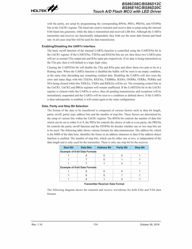
Rev. 1.10 174 October 09, 2018 Rev. 1.10 175 October 09, 2018
BS86C08C/BS86D12CBS86E16C/BS86D20C
Touch A/D Flash MCU with LED Driver
BS86C08C/BS86D12CBS86E16C/BS86D20CTouch A/D Flash MCU with LED Driver
with the parity, are setup by programming the corresponding BNOn, PRTn, PRENn, and STOPSn bits in the UnCR1 register. The baud rate used to transmit and receive data is setup using the internal 8-bit baud rate generator, while the data is transmitted and received LSB first. Although the UARTn transmitter and receiver are functionally independent, they both use the same data format and baud rate. In all cases stop bits will be used for data transmission.
Enabling/Disabling the UARTn InterfaceThe basic on/off function of the internal UARTn function is controlled using the UARTENn bit in the UnCR1 register. If the UARTENn, TXENn and RXENn bits are set, then these two UARTn pins will act as normal TXn output pin and RXn input pin respectively. If no data is being transmitted on the TXn pin, then it will default to a logic high value.
Clearing the UARTENn bit will disable the TXn and RXn pins and allow these two pins to be in a floating state. When the UARTn function is disabled the buffer will be reset to an empty condition, at the same time discarding any remaining residual data. Disabling the UARTn will also reset the error and status flags with bits TXENn, RXENn, TXBRKn, RXIFn, OERRn, FERRn, PERRn and NFn being cleared while bits TIDLEn, TXIFn and RIDLEn will be set. The remaining control bits in the UnCR1, UnCR2 and BRGn registers will remain unaffected. If the UARTENn bit in the UnCR1 register is cleared while the UARTn is active, then all pending transmissions and receptions will be immediately suspended and the UARTn will be reset to a condition as defined above. If the UARTn is then subsequently re-enabled, it will restart again in the same configuration.
Data, Parity and Stop Bit SelectionThe format of the data to be transferred is composed of various factors such as data bit length, parity on/off, parity type, address bits and the number of stop bits. These factors are determined by the setup of various bits within the UnCR1 register. The BNOn bit controls the number of data bits which can be set to either 8 or 9, the PRTn bit controls the choice of odd or even parity, the PRENn bit controls the parity on/off function and the STOPSn bit decides whether one or two stop bits are to be used. The following table shows various formats for data transmission. The address bit, which is the MSB of the data byte, identifies the frame as an address character or data if the address detect function is enabled. The number of stop bits, which can be either one or two, is independent of the data length and is only used for the transmitter. There is only one stop bit for the receiver.
Start Bit Data Bits Address Bit Parity Bit Stop BitExample of 8-bit Data Formats
1 8 0 0 11 7 0 1 11 7 1 0 1
Example of 9-bit Data Formats1 9 0 0 11 8 0 1 11 8 1 0 1
Transmitter Receiver Data Format
The following diagram shows the transmit and receive waveforms for both 8-bit and 9-bit data formats.

Rev. 1.10 174 October 09, 2018 Rev. 1.10 175 October 09, 2018
BS86C08C/BS86D12CBS86E16C/BS86D20C
Touch A/D Flash MCU with LED Driver
BS86C08C/BS86D12CBS86E16C/BS86D20CTouch A/D Flash MCU with LED Driver
Bit 0
8-bit data format
Bit 1 Stop Bit
NextStartBit
StartBit
Parity Bit
Bit 2 Bit 3 Bit 4 Bit 5 Bit 6 Bit 7
Bit 0
9-bit data format
Bit 1StartBit Bit 2 Bit 3 Bit 4 Bit 5 Bit 6 Stop
Bit
Next StartBit
Parity Bit
Bit 8Bit 7
UARTn TransmitterData word lengths of either 8 or 9 bits can be selected by programming the BNOn bit in the UnCR1 register. When BNOn bit is set, the word length will be set to 9 bits. In this case the 9th bit, which is the MSB, needs to be stored in the TX8n bit in the UnCR1 register. At the transmitter core lies the Transmitter Shift Register, more commonly known as the TSRn, whose data is obtained from the transmit data register, which is known as the TXR_RXRn register. The data to be transmitted is loaded into this TXR_RXRn register by the application program. The TSRn register is not written to with new data until the stop bit from the previous transmission has been sent out. As soon as this stop bit has been transmitted, the TSRn can then be loaded with new data from the TXR_RXRn register, if it is available. It should be noted that the TSRn register, unlike many other registers, is not directly mapped into the Data Memory area and as such is not available to the application program for direct read/write operations. An actual transmission of data will normally be enabled when the TXENn bit is set, but the data will not be transmitted until the TXR_RXRn register has been loaded with data and the baud rate generator has defined a shift clock source. However, the transmission can also be initiated by first loading data into the TXR_RXRn register, after which the TXENn bit can be set. When a transmission of data begins, the TSRn is normally empty, in which case a transfer to the TXR_RXRn register will result in an immediate transfer to the TSRn. If during a transmission the TXENn bit is cleared, the transmission will immediately cease and the transmitter will be reset. The TXn output pin can then be in a floating state.
Transmitting DataWhen the UARTn is transmitting data, the data is shifted on the TXn pin from the shift register, with the least significant bit first. In the transmit mode, the TXR_RXRn register forms a buffer between the internal bus and the transmitter shift register. It should be noted that if 9-bit data format has been selected, then the MSB will be taken from the TX8n bit in the UnCR1 register. The steps to initiate a data transfer can be summarized as follows:
• Make the correct selection of the BNOn, PRTn, PRENn and STOPSn bits to define the required word length, parity type and number of stop bits.
• Setup the BRGn register to select the desired baud rate.
• Set the TXENn bit to ensure that the TXn pin is used as a UARTn transmitter pin.
• Access the UnSR register and write the data that is to be transmitted into the TXR_RXRn register. Note that this step will clear the TXIFn bit.
This sequence of events can now be repeated to send additional data.
It should be noted that when TXIFn=0, data will be inhibited from being written to the TXR_RXRn register. Clearing the TXIFn flag is always achieved using the following software sequence:
1. A UnSR register access
2. A TXR_RXRn register write execution
The read-only TXIFn flag is set by the UARTn hardware and if set indicates that the TXR_RXRn register is empty and that other data can now be written into the TXR_RXRn register without

Rev. 1.10 176 October 09, 2018 Rev. 1.10 177 October 09, 2018
BS86C08C/BS86D12CBS86E16C/BS86D20C
Touch A/D Flash MCU with LED Driver
BS86C08C/BS86D12CBS86E16C/BS86D20CTouch A/D Flash MCU with LED Driver
overwriting the previous data. If the TEIEn bit is set then the TXIFn flag will generate an interrupt.
During a data transmission, a write instruction to the TXR_RXRn register will place the data into the TXR_RXRn register, which will be copied to the shift register at the end of the present transmission. When there is no data transmission in progress, a write instruction to the TXR_RXRn register will place the data directly into the shift register, resulting in the commencement of data transmission, and the TXIFn bit being immediately set. When a frame transmission is complete, which happens after stop bits are sent or after the break frame, the TIDLEn bit will be set. To clear the TIDLEn bit the following software sequence is used:
1. A UnSR register access
2. A TXR_RXRn register write execution
Note that both the TXIFn and TIDLEn bits are cleared by the same software sequence.
Transmit BreakIf the TXBRKn bit is set then break characters will be sent on the next transmission. Break character transmission consists of a start bit, followed by 13×N ‘0’ bits and stop bits, where N=1, 2, etc. If a break character is to be transmitted then the TXBRKn bit must be first set by the application program, and then cleared to generate the stop bits. Transmitting a break character will not generate a transmit interrupt. Note that a break condition length is at least 13 bits long. If the TXBRKn bit is continually kept at a logic high level then the transmitter circuitry will transmit continuous break characters. After the application program has cleared the TXBRKn bit, the transmitter will finish transmitting the last break character and subsequently send out one or two stop bits. The automatic logic highs at the end of the last break character will ensure that the start bit of the next frame is recognized.
UARTn ReceiverThe UARTn is capable of receiving word lengths of either 8 or 9 bits. If the BNOn bit is set, the word length will be set to 9 bits with the MSB being stored in the RX8n bit of the UnCR1 register. At the receiver core lies the Receive Serial Shift Register, commonly known as the RSRn. The data which is received on the RXn external input pin is sent to the data recovery block. The data recovery block operating speed is 16 times that of the baud rate, while the main receive serial shifter operates at the baud rate. After the RXn pin is sampled for the stop bit, the received data in RSRn is transferred to the receive data register, if the register is empty. The data which is received on the external RXn input pin is sampled three times by a majority detect circuit to determine the logic level that has been placed onto the RXn pin. It should be noted that the RSRn register, unlike many other registers, is not directly mapped into the Data Memory area and as such is not available to the application program for direct read/write operations.
Receiving DataWhen the UARTn receiver is receiving data, the data is serially shifted in on the external RXn input pin, LSB first. In the read mode, the TXR_RXRn register forms a buffer between the internal bus and the receiver shift register. The TXR_RXRn register is a two byte deep FIFO data buffer, where two bytes can be held in the FIFO while a third byte can continue to be received. Note that the application program must ensure that the data is read from TXR_RXRn before the third byte has been completely shifted in, otherwise this third byte will be discarded and an overrun error OERRn will be subsequently indicated. The steps to initiate a data transfer can be summarized as follows:
• Make the correct selection of BNOn, PRTn and PRENn bits to define the word length, parity type.
• Setup the BRGn register to select the desired baud rate.
• Set the RXENn bit to ensure that the RXn pin is used as a UARTn receiver pin.
Rev. 1.10 176 October 09, 2018 Rev. 1.10 177 October 09, 2018
BS86C08C/BS86D12CBS86E16C/BS86D20C
Touch A/D Flash MCU with LED Driver
BS86C08C/BS86D12CBS86E16C/BS86D20CTouch A/D Flash MCU with LED Driver
At this point the receiver will be enabled which will begin to look for a start bit.
When a character is received the following sequence of events will occur:
• The RXIFn bit in the UnSR register will be set when the TXR_RXRn register has data available. There will be at most one more character available before an overrun error occurs.
• When the contents of the shift register have been transferred to the TXR_RXRn register, then if the RIEn bit is set, an interrupt will be generated.
• If during reception, a frame error, noise error, parity error, or an overrun error has been detected, then the error flags can be set.
The RXIFn bit can be cleared using the following software sequence:
1. A UnSR register access
2. A TXR_RXRn register read execution
Receive BreakAny break character received by the UARTn will be managed as a framing error. The receiver will count and expect a certain number of bit times as specified by the values programmed into the BNOn bit plus one stop bit. If the break is much longer than 13 bit times, the reception will be considered as complete after the number of bit times specified by BNOn plus one stop bit. The RXIFn bit is set, FERRn is set, zeros are loaded into the receive data register, interrupts are generated if appropriate and the RIDLEn bit is set. A break is regarded as a character that contains only zeros with the FERRn flag set. If a long break signal has been detected, the receiver will regard it as a data frame including a start bit, data bits and the invalid stop bit and the FERRn flag will be set. The receiver must wait for a valid stop bit before looking for the next start bit. The receiver will not make the assumption that the break condition on the line is the next start bit. The break character will be loaded into the buffer and no further data will be received until stop bits are received. It should be noted that the RIDLEn read only flag will go high when the stop bits have not yet been received. The reception of a break character on the UARTn registers will result in the following:
• The framing error flag, FERRn, will be set.
• The receive data register, TXR_RXRn, will be cleared.
• The OERRn, NFn, PERRn, RIDLEn or RXIFn flags will possibly be set.
Idle StatusWhen the receiver is reading data, which means it will be in between the detection of a start bit and the reading of a stop bit, the receiver status flag in the UnSR register, otherwise known as the RIDLEn flag, will have a zero value. In between the reception of a stop bit and the detection of the next start bit, the RIDLEn flag will have a high value, which indicates the receiver is in an idle condition.
Receiver InterruptThe read only receive interrupt flag RXIFn in the UnSR register is set by an edge generated by the receiver. An interrupt is generated if RIEn=1, when a word is transferred from the Receive Shift Register, RSRn, to the Receive Data Register, TXR_RXRn. An overrun error can also generate an interrupt if RIEn=1.
Managing Receiver ErrorsSeveral types of reception errors can occur within the UARTn module, the following section describes the various types and how they are managed by the UARTn.

Rev. 1.10 178 October 09, 2018 Rev. 1.10 179 October 09, 2018
BS86C08C/BS86D12CBS86E16C/BS86D20C
Touch A/D Flash MCU with LED Driver
BS86C08C/BS86D12CBS86E16C/BS86D20CTouch A/D Flash MCU with LED Driver
Overrun Error – OERRnThe TXR_RXRn register is composed of a two byte deep FIFO data buffer, where two bytes can be held in the FIFO register, while a third byte can continue to be received. Before this third byte has been entirely shifted in, the data should be read from the TXR_RXRn register. If this is not done, the overrun error flag OERRn will be consequently indicated.
In the event of an overrun error occurring, the following will happen:
• The OERRn flag in the UnSR register will be set.
• The TXR_RXRn contents will not be lost.
• The shift register will be overwritten.
• An interrupt will be generated if the RIEn bit is set.
The OERRn flag can be cleared by an access to the UnSR register followed by a read to the TXR_RXRn register.
Noise Error – NFnOver-sampling is used for data recovery to identify valid incoming data and noise. If noise is detected within a frame the following will occur:
• The read only noise flag, NFn, in the UnSR register will be set on the rising edge of the RXIFn bit.
• Data will be transferred from the Shift register to the TXR_RXRn register.
• No interrupt will be generated. However this bit rises at the same time as the RXIFn bit which itself generates an interrupt.
Note that the NFn flag is reset by an UnSR register read operation followed by a TXR_RXRn register read operation.
Framing Error – FERRnThe read only framing error flag, FERRn, in the UnSR register, is set if a zero is detected instead of stop bits. If two stop bits are selected, both stop bits must be high; otherwise the FERRn flag will be set. The FERRn flag and the received data will be recorded in the UnSR and TXR_RXRn registers respectively, and the flag is cleared in any reset.
Parity Error – PERRnThe read only parity error flag, PERRn, in the UnSR register, is set if the parity of the received word is incorrect. This error flag is only applicable if the parity is enabled, PRENn=1, and if the parity type, odd or even is selected. The read only PERRn flag and the received data will be recorded in the UnSR and TXR_RXRn registers respectively. It is cleared on any reset, it should be noted that the flags, FERRn and PERRn, in the UnSR register should first be read by the application program before reading the data word.
UARTn Interrupt StructureSeveral individual UARTn conditions can generate a UARTn interrupt. When these conditions exist, a low pulse will be generated to get the attention of the microcontroller. These conditions are a transmitter data register empty, transmitter idle, receiver data available, receiver overrun, address detect and an RXn pin wake-up. When any of these conditions are created, if the global interrupt enable bit and its corresponding interrupt control bit are enabled and the stack is not full, the program will jump to its corresponding interrupt vector where it can be serviced before returning to the main program. Four of these conditions have the corresponding UnSR register flags which will generate a UARTn interrupt if its associated interrupt enable control bit in the UnCR2 register is set. The two transmitter interrupt conditions have their own corresponding enable control bits, while the
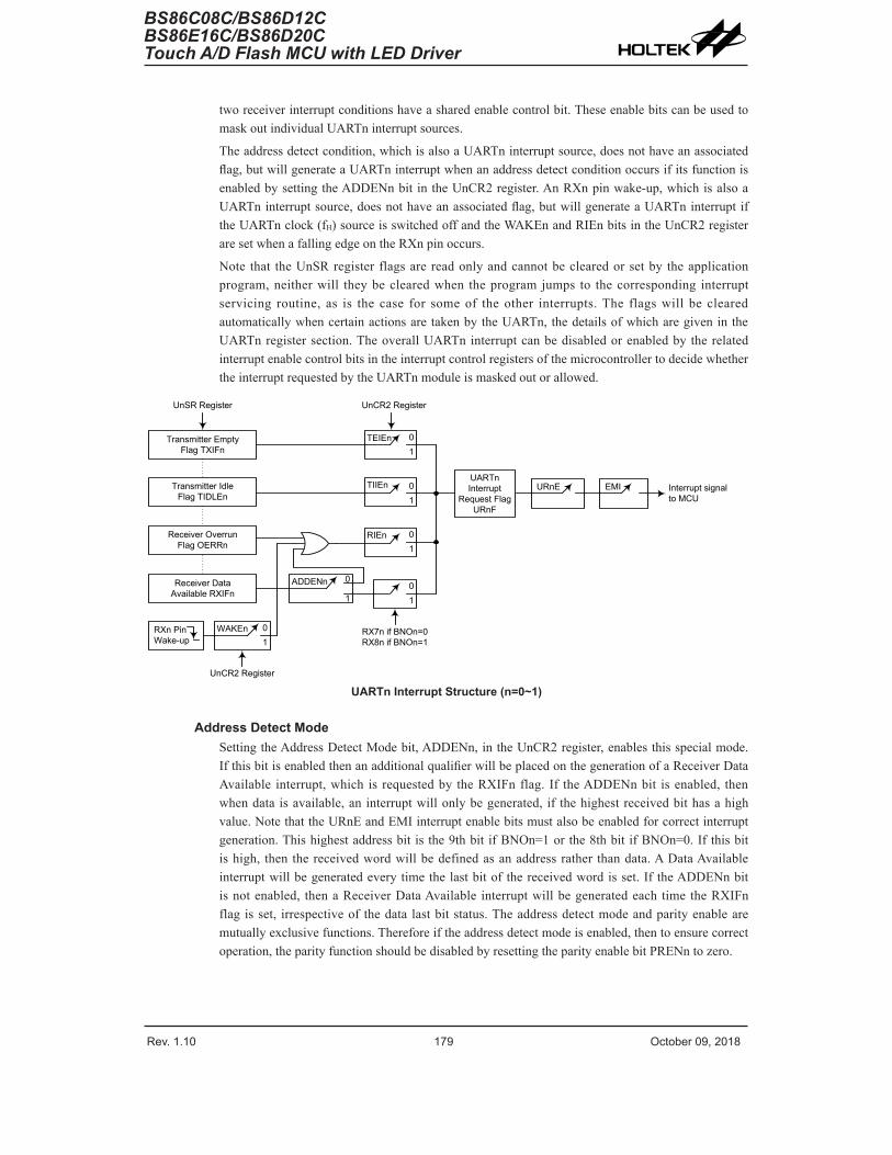
Rev. 1.10 178 October 09, 2018 Rev. 1.10 179 October 09, 2018
BS86C08C/BS86D12CBS86E16C/BS86D20C
Touch A/D Flash MCU with LED Driver
BS86C08C/BS86D12CBS86E16C/BS86D20CTouch A/D Flash MCU with LED Driver
two receiver interrupt conditions have a shared enable control bit. These enable bits can be used to mask out individual UARTn interrupt sources.
The address detect condition, which is also a UARTn interrupt source, does not have an associated flag, but will generate a UARTn interrupt when an address detect condition occurs if its function is enabled by setting the ADDENn bit in the UnCR2 register. An RXn pin wake-up, which is also a UARTn interrupt source, does not have an associated flag, but will generate a UARTn interrupt if the UARTn clock (fH) source is switched off and the WAKEn and RIEn bits in the UnCR2 register are set when a falling edge on the RXn pin occurs.
Note that the UnSR register flags are read only and cannot be cleared or set by the application program, neither will they be cleared when the program jumps to the corresponding interrupt servicing routine, as is the case for some of the other interrupts. The flags will be cleared automatically when certain actions are taken by the UARTn, the details of which are given in the UARTn register section. The overall UARTn interrupt can be disabled or enabled by the related interrupt enable control bits in the interrupt control registers of the microcontroller to decide whether the interrupt requested by the UARTn module is masked out or allowed.
Transmitter EmptyFlag TXIFn
UnSR Register
Transmitter IdleFlag TIDLEn
Receiver OverrunFlag OERRn
Receiver DataAvailable RXIFn
ADDENn
RXn PinWake-up
WAKEn 01
0
1
RX7n if BNOn=0RX8n if BNOn=1
UnCR2 Register
RIEn 01
TIIEn 01
TEIEn 01
UARTn Interrupt
Request Flag URnF
UnCR2 Register
URnE EMI
01
Interrupt signal to MCU
UARTn Interrupt Structure (n=0~1)
Address Detect ModeSetting the Address Detect Mode bit, ADDENn, in the UnCR2 register, enables this special mode. If this bit is enabled then an additional qualifier will be placed on the generation of a Receiver Data Available interrupt, which is requested by the RXIFn flag. If the ADDENn bit is enabled, then when data is available, an interrupt will only be generated, if the highest received bit has a high value. Note that the URnE and EMI interrupt enable bits must also be enabled for correct interrupt generation. This highest address bit is the 9th bit if BNOn=1 or the 8th bit if BNOn=0. If this bit is high, then the received word will be defined as an address rather than data. A Data Available interrupt will be generated every time the last bit of the received word is set. If the ADDENn bit is not enabled, then a Receiver Data Available interrupt will be generated each time the RXIFn flag is set, irrespective of the data last bit status. The address detect mode and parity enable are mutually exclusive functions. Therefore if the address detect mode is enabled, then to ensure correct operation, the parity function should be disabled by resetting the parity enable bit PRENn to zero.
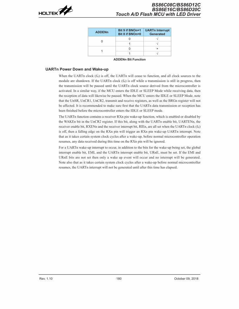
Rev. 1.10 180 October 09, 2018 Rev. 1.10 181 October 09, 2018
BS86C08C/BS86D12CBS86E16C/BS86D20C
Touch A/D Flash MCU with LED Driver
BS86C08C/BS86D12CBS86E16C/BS86D20CTouch A/D Flash MCU with LED Driver
ADDENn Bit 9 if BNOn=1Bit 8 if BNOn=0
UARTn InterruptGenerated
00 √1 √
10 ×1 √
ADDENn Bit Function
UARTn Power Down and Wake-upWhen the UARTn clock (fH) is off, the UARTn will cease to function, and all clock sources to the module are shutdown. If the UARTn clock (fH) is off while a transmission is still in progress, then the transmission will be paused until the UARTn clock source derived from the microcontroller is activated. In a similar way, if the MCU enters the IDLE or SLEEP Mode while receiving data, then the reception of data will likewise be paused. When the MCU enters the IDLE or SLEEP Mode, note that the UnSR, UnCR1, UnCR2, transmit and receive registers, as well as the BRGn register will not be affected. It is recommended to make sure first that the UARTn data transmission or reception has been finished before the microcontroller enters the IDLE or SLEEP mode.
The UARTn function contains a receiver RXn pin wake-up function, which is enabled or disabled by the WAKEn bit in the UnCR2 register. If this bit, along with the UARTn enable bit, UARTENn, the receiver enable bit, RXENn and the receiver interrupt bit, RIEn, are all set when the UARTn clock (fH) is off, then a falling edge on the RXn pin will trigger an RXn pin wake-up UARTn interrupt. Note that as it takes certain system clock cycles after a wake-up, before normal microcontroller operation resumes, any data received during this time on the RXn pin will be ignored.
For a UARTn wake-up interrupt to occur, in addition to the bits for the wake-up being set, the global interrupt enable bit, EMI, and the UARTn interrupt enable bit, URnE, must be set. If the EMI and URnE bits are not set then only a wake up event will occur and no interrupt will be generated. Note also that as it takes certain system clock cycles after a wake-up before normal microcontroller resumes, the UARTn interrupt will not be generated until after this time has elapsed.

Rev. 1.10 180 October 09, 2018 Rev. 1.10 181 October 09, 2018
BS86C08C/BS86D12CBS86E16C/BS86D20C
Touch A/D Flash MCU with LED Driver
BS86C08C/BS86D12CBS86E16C/BS86D20CTouch A/D Flash MCU with LED Driver
Low Voltage Detector – LVDEach device has a Low Voltage Detector function, also known as LVD. This enabled the device to monitor the power supply voltage, VDD, and provide a warning signal should it fall below a certain level. This function may be especially useful in battery applications where the supply voltage will gradually reduce as the battery ages, as it allows an early warning battery low signal to be generated. The Low Voltage Detector also has the capability of generating an interrupt signal.
LVD RegisterThe Low Voltage Detector function is controlled using a single register with the name LVDC. Three bits in this register, VLVD2~VLVD0, are used to select one of eight fixed voltages below which a low voltage condition will be determined. A low voltage condition is indicated when the LVDO bit is set. If the LVDO bit is low, this indicates that the VDD voltage is above the preset low voltage value. The LVDEN bit is used to control the overall on/off function of the low voltage detector. Setting the bit high will enable the low voltage detector. Clearing the bit to zero will switch off the internal low voltage detector circuits. As the low voltage detector will consume a certain amount of power, it may be desirable to switch off the circuit when not in use, an important consideration in power sensitive battery powered applications.
• LVDC Register
Bit 7 6 5 4 3 2 1 0Name — — LVDO LVDEN VBGEN VLVD2 VLVD1 VLVD0R/W — — R R/W R/W R/W R/W R/WPOR — — 0 0 0 0 0 0
Bit 7~6 Unimplemented, read as “0”Bit 5 LVDO: LVD Output Flag
0: No Low Voltage Detect1: Low Voltage Detect
Bit 4 LVDEN: Low Voltage Detector Control0: Disable1: Enable
Bit 3 VBGEN: Bandgap Buffer Control0: Disable1: Enable
Note that the Bandgap circuit is enabled when the LVD or LVR function is enabled or when the VBGEN bit is set to 1.
Bit 2~0 VLVD2~VLVD0: Select LVD Voltage000: 2.0V001: 2.2V010: 2.4V011: 2.7V100: 3.0V101: 3.3V110: 3.6V111: 4.0V
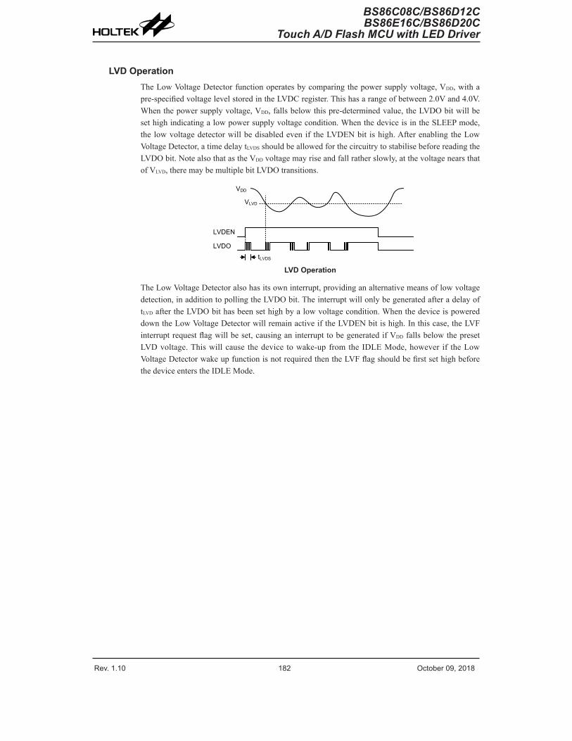
Rev. 1.10 182 October 09, 2018 Rev. 1.10 183 October 09, 2018
BS86C08C/BS86D12CBS86E16C/BS86D20C
Touch A/D Flash MCU with LED Driver
BS86C08C/BS86D12CBS86E16C/BS86D20CTouch A/D Flash MCU with LED Driver
LVD OperationThe Low Voltage Detector function operates by comparing the power supply voltage, VDD, with a pre-specified voltage level stored in the LVDC register. This has a range of between 2.0V and 4.0V. When the power supply voltage, VDD, falls below this pre-determined value, the LVDO bit will be set high indicating a low power supply voltage condition. When the device is in the SLEEP mode, the low voltage detector will be disabled even if the LVDEN bit is high. After enabling the Low Voltage Detector, a time delay tLVDS should be allowed for the circuitry to stabilise before reading the LVDO bit. Note also that as the VDD voltage may rise and fall rather slowly, at the voltage nears that of VLVD, there may be multiple bit LVDO transitions.
VDD
LVDEN
LVDO
VLVD
tLVDS
LVD Operation
The Low Voltage Detector also has its own interrupt, providing an alternative means of low voltage detection, in addition to polling the LVDO bit. The interrupt will only be generated after a delay of tLVD after the LVDO bit has been set high by a low voltage condition. When the device is powered down the Low Voltage Detector will remain active if the LVDEN bit is high. In this case, the LVF interrupt request flag will be set, causing an interrupt to be generated if VDD falls below the preset LVD voltage. This will cause the device to wake-up from the IDLE Mode, however if the Low Voltage Detector wake up function is not required then the LVF flag should be first set high before the device enters the IDLE Mode.

Rev. 1.10 182 October 09, 2018 Rev. 1.10 183 October 09, 2018
BS86C08C/BS86D12CBS86E16C/BS86D20C
Touch A/D Flash MCU with LED Driver
BS86C08C/BS86D12CBS86E16C/BS86D20CTouch A/D Flash MCU with LED Driver
InterruptsInterrupts are an important part of any microcontroller system. When an external event or an internal function such as a Timer Module or an A/D converter requires microcontroller attention, their corresponding interrupt will enforce a temporary suspension of the main program allowing the microcontroller to direct attention to their respective needs. These devices contain an external interrupt and several internal interrupt functions. The external interrupt is generated by the action of the external INT pin, while the internal interrupts are generated by various internal functions such as the TMs, Time Base, LVD, EEPROM, UART and the A/D converter, etc.
Interrupt RegistersOverall interrupt control, which basically means the setting of request flags when certain microcontroller conditions occur and the setting of interrupt enable bits by the application program, is controlled by a series of registers, located in the Special Purpose Data Memory, as shown in the accompanying table. The number of registers depends upon the device chosen but fall into three categories. The first is the INTC0~INTC3 registers which setup the primary interrupts. The second is the MFI register which setups the Multi-function interrupt. Finally there is an INTEG register to setup the external interrupt trigger edge type.
Each register contains a number of enable bits to enable or disable individual interrupts as well as interrupt flags to indicate the presence of an interrupt request. The naming convention of these follows a specific pattern. First is listed an abbreviated interrupt type, then the (optional) number of that interrupt followed by either an “E” for enable/disable bit or “F” for request flag.
Function Enable Bit Request Flag Notes
Global EMI — —INT Pin INTE INTF —Touch Key Module TKME TKMF —
Time Base TBnE TBnF n=0 for BS86C08C/BS86D12Cn=0~1 for BS86E16C/BS86D20C
I2C IICE IICF For BS86C08C/BS86D12C/BS86E16CSIM SIME SIMF For BS86D20CEEPROM write operation DEE DEF —
UART URnE URnF n=0 for BS86C08C/BS86D12C/BS86D20Cn=0~1 for BS86E16C
LVD LVE LVF —A/D Converter ADE ADF —Multi-function MFE MFF For BS86E16C/BS86D20C
CTMCTMnPE CTMnPF
n=0CTMnAE CTMnAF
PTMPTMnPE PTMnPF n=0 for BS86C08C/BS86D12C
n=0~1 for BS86E16C/BS86D20CPTMnAE PTMnAF
Interrupt Register Bit Naming Conventions

Rev. 1.10 184 October 09, 2018 Rev. 1.10 185 October 09, 2018
BS86C08C/BS86D12CBS86E16C/BS86D20C
Touch A/D Flash MCU with LED Driver
BS86C08C/BS86D12CBS86E16C/BS86D20CTouch A/D Flash MCU with LED Driver
Register Name
Bit
7 6 5 4 3 2 1 0INTEG — — — — — — INTS1 INTS0INTC0 — TB0F TKMF INTF TB0E TKME INTE EMIINTC1 PTM0AF PTM0PF CTM0AF CTM0PF PTM0AE PTM0PE CTM0AE CTM0PEINTC2 LVF UR0F DEF IICF LVE UR0E DEE IICEINTC3 — — — ADF — — — ADE
Interrupt Register List – BS86C08C/BS86D12C
Register Name
Bit
7 6 5 4 3 2 1 0INTEG — — — — — — INTS1 INTS0INTC0 — TB0F TKMF INTF TB0E TKME INTE EMIINTC1 PTM0AF PTM0PF CTM0AF CTM0PF PTM0AE PTM0PE CTM0AE CTM0PEINTC2 LVF UR0F DEF IICF LVE UR0E DEE IICEINTC3 MFF UR1F TB1F ADF MFE UR1E TB1E ADE
MFI — — PTM1AF PTM1PF — — PTM1AE PTM1PE
Interrupt Register List – BS86E16C
Register Name
Bit
7 6 5 4 3 2 1 0
INTEG — — — — — — INTS1 INTS0INTC0 — TB0F TKMF INTF TB0E TKME INTE EMIINTC1 PTM0AF PTM0PF CTM0AF CTM0PF PTM0AE PTM0PE CTM0AE CTM0PEINTC2 LVF UR0F DEF SIMF LVE UR0E DEE SIMEINTC3 MFF — TB1F ADF MFE — TB1E ADE
MFI — — PTM1AF PTM1PF — — PTM1AE PTM1PE
Interrupt Register List – BS86D20C
• INTEG Register
Bit 7 6 5 4 3 2 1 0Name — — — — — — INTS1 INTS0R/W — — — — — — R/W R/WPOR — — — — — — 0 0
Bit 7~4 Unimplemented, read as “0”Bit 1~0 INTS1~INTS0: Interrupt edge control for INT pin
00: Disable01: Rising edge10: Falling edge11: Rising and falling edges

Rev. 1.10 184 October 09, 2018 Rev. 1.10 185 October 09, 2018
BS86C08C/BS86D12CBS86E16C/BS86D20C
Touch A/D Flash MCU with LED Driver
BS86C08C/BS86D12CBS86E16C/BS86D20CTouch A/D Flash MCU with LED Driver
• INTC0 Register
Bit 7 6 5 4 3 2 1 0Name — TB0F TKMF INTF TB0E TKME INTE EMIR/W — R/W R/W R/W R/W R/W R/W R/WPOR — 0 0 0 0 0 0 0
Bit 7 Unimplemented, read as “0”Bit 6 TB0F: Time Base 0 interrupt request flag
0: No request1: Interrupt request
Bit 5 TKMF: Touch key module interrupt request flag0: No request1: Interrupt request
Bit 4 INTF: INT interrupt request flag0: No request1: Interrupt request
Bit 3 TB0E: Time Base 0 interrupt control0: Disable1: Enable
Bit 2 TKME: Touch key module interrupt control0: Disable1: Enable
Bit 1 INTE: INT interrupt control0: Disable1: Enable
Bit 0 EMI: Global interrupt control0: Disable1: Enable
• INTC1 Register
Bit 7 6 5 4 3 2 1 0Name PTM0AF PTM0PF CTM0AF CTM0PF PTM0AE PTM0PE CTM0AE CTM0PER/W R/W R/W R/W R/W R/W R/W R/W R/WPOR 0 0 0 0 0 0 0 0
Bit 7 PTM0AF: PTM0 Comparator A match interrupt request flag0: No request1: Interrupt request
Bit 6 PTM0PF: PTM0 Comparator P match interrupt request flag0: No request1: Interrupt request
Bit 5 CTM0AF: CTM0 Comparator A match interrupt request flag0: No request1: Interrupt request
Bit 4 CTM0PF: CTM0 Comparator P match interrupt request flag0: No request1: Interrupt request
Bit 3 PTM0AE: PTM0 Comparator A match interrupt control0: Disable1: Enable
Bit 2 PTM0PE: PTM0 Comparator P match interrupt control0: Disable1: Enable
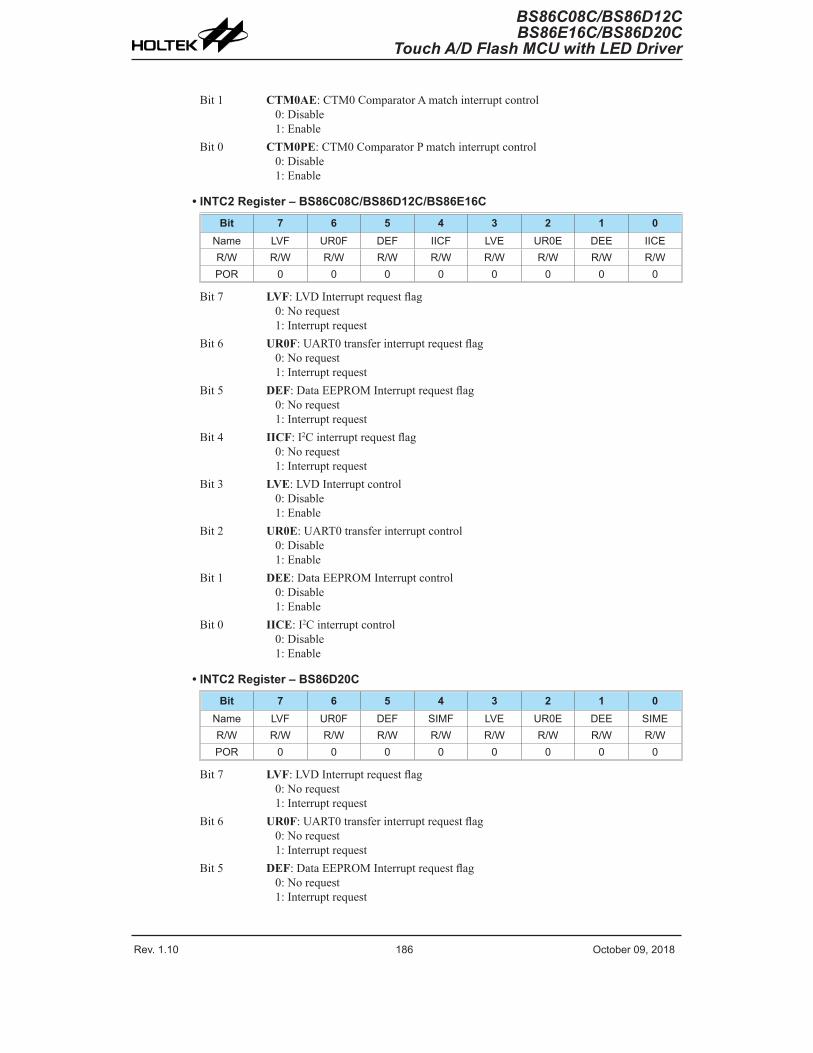
Rev. 1.10 186 October 09, 2018 Rev. 1.10 187 October 09, 2018
BS86C08C/BS86D12CBS86E16C/BS86D20C
Touch A/D Flash MCU with LED Driver
BS86C08C/BS86D12CBS86E16C/BS86D20CTouch A/D Flash MCU with LED Driver
Bit 1 CTM0AE: CTM0 Comparator A match interrupt control0: Disable1: Enable
Bit 0 CTM0PE: CTM0 Comparator P match interrupt control0: Disable1: Enable
• INTC2 Register – BS86C08C/BS86D12C/BS86E16C
Bit 7 6 5 4 3 2 1 0Name LVF UR0F DEF IICF LVE UR0E DEE IICER/W R/W R/W R/W R/W R/W R/W R/W R/WPOR 0 0 0 0 0 0 0 0
Bit 7 LVF: LVD Interrupt request flag0: No request1: Interrupt request
Bit 6 UR0F: UART0 transfer interrupt request flag0: No request1: Interrupt request
Bit 5 DEF: Data EEPROM Interrupt request flag0: No request1: Interrupt request
Bit 4 IICF: I2C interrupt request flag0: No request1: Interrupt request
Bit 3 LVE: LVD Interrupt control0: Disable1: Enable
Bit 2 UR0E: UART0 transfer interrupt control0: Disable1: Enable
Bit 1 DEE: Data EEPROM Interrupt control0: Disable1: Enable
Bit 0 IICE: I2C interrupt control0: Disable1: Enable
• INTC2 Register – BS86D20C
Bit 7 6 5 4 3 2 1 0Name LVF UR0F DEF SIMF LVE UR0E DEE SIMER/W R/W R/W R/W R/W R/W R/W R/W R/WPOR 0 0 0 0 0 0 0 0
Bit 7 LVF: LVD Interrupt request flag0: No request1: Interrupt request
Bit 6 UR0F: UART0 transfer interrupt request flag0: No request1: Interrupt request
Bit 5 DEF: Data EEPROM Interrupt request flag0: No request1: Interrupt request

Rev. 1.10 186 October 09, 2018 Rev. 1.10 187 October 09, 2018
BS86C08C/BS86D12CBS86E16C/BS86D20C
Touch A/D Flash MCU with LED Driver
BS86C08C/BS86D12CBS86E16C/BS86D20CTouch A/D Flash MCU with LED Driver
Bit 4 SIMF: SIM interrupt request flag0: No request1: Interrupt request
Bit 3 LVE: LVD Interrupt control0: Disable1: Enable
Bit 2 UR0E: UART0 transfer interrupt control0: Disable1: Enable
Bit 1 DEE: Data EEPROM Interrupt control0: Disable1: Enable
Bit 0 SIME: SIM interrupt control0: Disable1: Enable
• INTC3 Register – BS86C08C/BS86D12C
Bit 7 6 5 4 3 2 1 0Name — — — ADF — — — ADER/W — — — R/W — — — R/WPOR — — — 0 — — — 0
Bit 7~5 Unimplemented, read as “0”Bit 4 ADF: A/D Converter interrupt request flag
0: No request1: Interrupt request
Bit 3~1 Unimplemented, read as “0”Bit 0 ADE: A/D Converter interrupt control
0: Disable1: Enable
• INTC3 Register – BS86E16C
Bit 7 6 5 4 3 2 1 0Name MFF UR1F TB1F ADF MFE UR1E TB1E ADER/W R/W R/W R/W R/W R/W R/W R/W R/WPOR 0 0 0 0 0 0 0 0
Bit 7 MFF: Multi-function interrupt request flag0: No request1: Interrupt request
Bit 6 UR1F: UART1 transfer interrupt request flag0: No request1: Interrupt request
Bit 5 TB1F: Time Base 1 interrupt request flag0: No request1: Interrupt request
Bit 4 ADF: A/D Converter interrupt request flag0: No request1: Interrupt request
Bit 3 MFE: Multi-function interrupt control0: Disable1: Enable
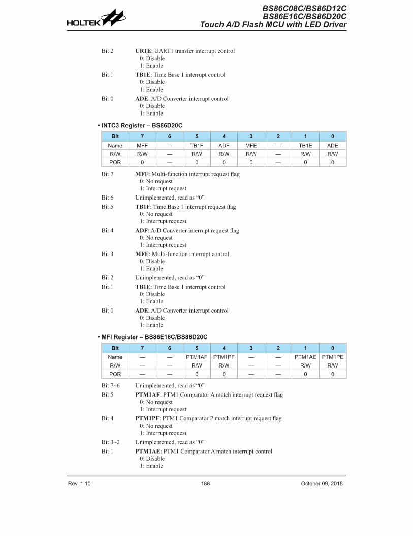
Rev. 1.10 188 October 09, 2018 Rev. 1.10 189 October 09, 2018
BS86C08C/BS86D12CBS86E16C/BS86D20C
Touch A/D Flash MCU with LED Driver
BS86C08C/BS86D12CBS86E16C/BS86D20CTouch A/D Flash MCU with LED Driver
Bit 2 UR1E: UART1 transfer interrupt control0: Disable1: Enable
Bit 1 TB1E: Time Base 1 interrupt control0: Disable1: Enable
Bit 0 ADE: A/D Converter interrupt control0: Disable1: Enable
• INTC3 Register – BS86D20C
Bit 7 6 5 4 3 2 1 0Name MFF — TB1F ADF MFE — TB1E ADER/W R/W — R/W R/W R/W — R/W R/WPOR 0 — 0 0 0 — 0 0
Bit 7 MFF: Multi-function interrupt request flag0: No request1: Interrupt request
Bit 6 Unimplemented, read as “0”Bit 5 TB1F: Time Base 1 interrupt request flag
0: No request1: Interrupt request
Bit 4 ADF: A/D Converter interrupt request flag0: No request1: Interrupt request
Bit 3 MFE: Multi-function interrupt control0: Disable1: Enable
Bit 2 Unimplemented, read as “0”Bit 1 TB1E: Time Base 1 interrupt control
0: Disable1: Enable
Bit 0 ADE: A/D Converter interrupt control0: Disable1: Enable
• MFI Register – BS86E16C/BS86D20C
Bit 7 6 5 4 3 2 1 0Name — — PTM1AF PTM1PF — — PTM1AE PTM1PER/W — — R/W R/W — — R/W R/WPOR — — 0 0 — — 0 0
Bit 7~6 Unimplemented, read as “0”Bit 5 PTM1AF: PTM1 Comparator A match interrupt request flag
0: No request1: Interrupt request
Bit 4 PTM1PF: PTM1 Comparator P match interrupt request flag0: No request1: Interrupt request
Bit 3~2 Unimplemented, read as “0”Bit 1 PTM1AE: PTM1 Comparator A match interrupt control
0: Disable1: Enable

Rev. 1.10 188 October 09, 2018 Rev. 1.10 189 October 09, 2018
BS86C08C/BS86D12CBS86E16C/BS86D20C
Touch A/D Flash MCU with LED Driver
BS86C08C/BS86D12CBS86E16C/BS86D20CTouch A/D Flash MCU with LED Driver
Bit 0 PTM1PE: PTM1 Comparator P match interrupt control0: Disable1: Enable
Interrupt OperationWhen the conditions for an interrupt event occur, such as a Touch Key Counter overflow, a TM Comparator P or Comparator A match or A/D conversion completion, etc., the relevant interrupt request flag will be set. Whether the request flag actually generates a program jump to the relevant interrupt vector is determined by the condition of the interrupt enable bit. If the enable bit is set high then the program will jump to its relevant vector; if the enable bit is zero then although the interrupt request flag is set an actual interrupt will not be generated and the program will not jump to the relevant interrupt vector. The global interrupt enable bit, if cleared to zero, will disable all interrupts.
When an interrupt is generated, the Program Counter, which stores the address of the next instruction to be executed, will be transferred onto the stack. The Program Counter will then be loaded with a new address which will be the value of the corresponding interrupt vector. The microcontroller will then fetch its next instruction from this interrupt vector. The instruction at this vector will usually be a JMP which will jump to another section of program which is known as the interrupt service routine. Here is located the code to control the appropriate interrupt. The interrupt service routine must be terminated with a RETI, which retrieves the original Program Counter address from the stack and allows the microcontroller to continue with normal execution at the point where the interrupt occurred.
The various interrupt enable bits, together with their associated request flags, are shown in the accompanying diagrams with their order of priority. Some interrupt sources have their own individual vector while others share the same multi-function interrupt vector. Once an interrupt subroutine is serviced, all other interrupts will be blocked, as the global interrupt enable bit, EMI bit will be cleared automatically. This will prevent any further interrupt nesting from occurring. However, if other interrupt requests occur during this interval, although the interrupt will not be immediately serviced, the request flag will still be recorded.
If an interrupt requires immediate servicing while the program is already in another interrupt service routine, the EMI bit should be set after entering the routine to allow interrupt nesting. If the stack is full, the interrupt request will not be acknowledged, even if the related interrupt is enabled, until the Stack Pointer is decremented. If immediate service is desired, the stack must be prevented from becoming full. In case of simultaneous requests, the accompanying diagram shows the priority that is applied. All of the interrupt request flags when set will wake-up the device if it is in SLEEP or IDLE Mode, however to prevent a wake-up from occurring the corresponding flag should be set before the device is in SLEEP or IDLE Mode.
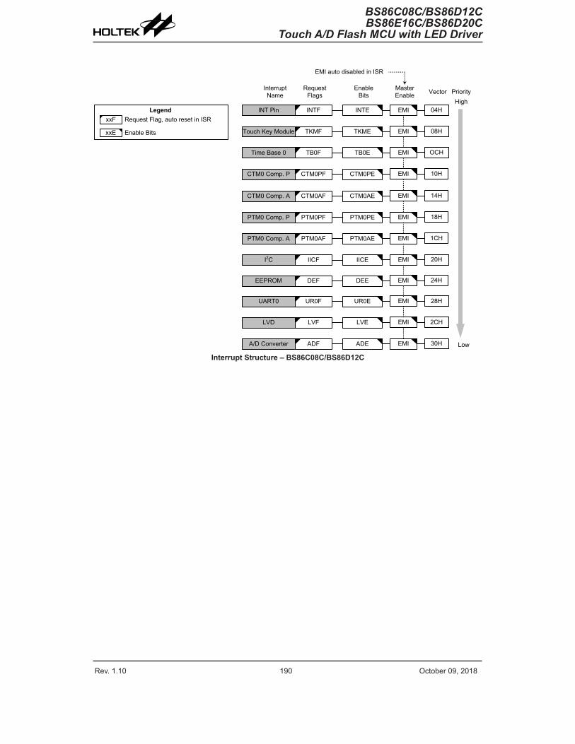
Rev. 1.10 190 October 09, 2018 Rev. 1.10 191 October 09, 2018
BS86C08C/BS86D12CBS86E16C/BS86D20C
Touch A/D Flash MCU with LED Driver
BS86C08C/BS86D12CBS86E16C/BS86D20CTouch A/D Flash MCU with LED Driver
Interrupt Name
RequestFlags
Enable Bits
MasterEnable Vector
EMI auto disabled in ISR
PriorityHigh
Low
04HINT Pin INTF INTE EMI
20HI2C IICF IICE EMI
EMI 08HTouch Key Module TKMF TKME
EMI OCHTime Base 0 TB0F TB0E
EMI 10HCTM0 Comp. P CTM0PF CTM0PE
EMI 14HCTM0 Comp. A CTM0AF CTM0AE
EMI 18HPTM0 Comp. P PTM0PF PTM0PE
1CHPTM0 Comp. A PTM0AF PTM0AE EMI
24HEEPROM DEF DEE EMI
UART0 UR0F UR0E EMI
EMILVD LVF LVE
28H
2CH
EMIA/D Converter ADF ADE 30H
Legend
xxE Enable Bits
xxF Request Flag, auto reset in ISR
Interrupt Structure – BS86C08C/BS86D12C

Rev. 1.10 190 October 09, 2018 Rev. 1.10 191 October 09, 2018
BS86C08C/BS86D12CBS86E16C/BS86D20C
Touch A/D Flash MCU with LED Driver
BS86C08C/BS86D12CBS86E16C/BS86D20CTouch A/D Flash MCU with LED Driver
Interrupt Name
Request Flags
Enable Bits
Master Enable Vector
EMI auto disabled in ISR
PriorityHigh
Low
Interrupts contained within Multi-Function Interrupts
PTM1 Comp. A PTM1AF PTM1AE
04HINT Pin INTF INTE EMI
20HI2C IICF IICE EMI
EMI 08HTouch Key Module TKMF TKME
InterruptName
Request Flags
Enable Bits
EMI OCHTime Base 0 TB0F TB0E
EMI 10HCTM0 Comp. P CTM0PF CTM0PE
EMI 14HCTM0 Comp. A CTM0AF CTM0AE
EMI 18HPTM0 Comp. P PTM0PF PTM0PE
1CHPTM0 Comp. A PTM0AF PTM0AE EMI
24HEEPROM DEF DEE EMI
PTM1 Comp. P PTM1PF PTM1PE
UART0 UR0F UR0E EMI
EMILVD LVF LVE
28H
2CH
EMIA/D Converter ADF ADE 30H
EMITime Base 1 TB1F TB1E 34H
UART1 UR1F UR1E EMI
EMIMulti-Function MFF MFE
38H
3CH
xxE Enable Bits
xxF Request Flag, auto reset in ISR
LegendxxF Request Flag, no auto reset in ISR
Interrupt Structure – BS86E16C

Rev. 1.10 192 October 09, 2018 Rev. 1.10 193 October 09, 2018
BS86C08C/BS86D12CBS86E16C/BS86D20C
Touch A/D Flash MCU with LED Driver
BS86C08C/BS86D12CBS86E16C/BS86D20CTouch A/D Flash MCU with LED Driver
Interrupt Name
Request Flags
Enable Bits
Master Enable Vector
EMI auto disabled in ISR
PriorityHigh
Low
04HINT Pin INTF INTE EMI
20HSIM SIMF SIME EMI
EMI 08HTouch Key Module TKMF TKME
EMI OCHTime Base 0 TB0F TB0E
EMI 10HCTM0 Comp. P CTM0PF CTM0PE
EMI 14HCTM0 Comp. A CTM0AF CTM0AE
EMI 18HPTM0 Comp. P PTM0PF PTM0PE
1CHPTM0 Comp. A PTM0AF PTM0AE EMI
24HEEPROM DEF DEE EMI
UART0 UR0F UR0E EMI
EMILVD LVF LVE
28H
2CH
EMIA/D Converter ADF ADE 30H
EMITime Base 1 TB1F TB1E 34H
xxE Enable Bits
xxF Request Flag, auto reset in ISR
LegendxxF Request Flag, no auto reset in ISR
Interrupts contained within Multi-Function Interrupts
PTM1 Comp. A PTM1AF PTM1AE
Interrupt Name
Request Flags
Enable Bits
PTM1 Comp. P PTM1PF PTM1PE
EMIMulti-Function MFF MFE 3CH
Interrupt Structure – BS86D20C
External InterruptThe external interrupt is controlled by signal transitions on the INT pin. An external interrupt request will take place when the external interrupt request flag, INTF, is set, which will occur when a transition, whose type is chosen by the edge select bits, appears on the external interrupt pin. To allow the program to branch to its respective interrupt vector address, the global interrupt enable bit, EMI, and respective external interrupt enable bit, INTE, must first be set. Additionally the correct interrupt edge type must be selected using the INTEG register to enable the external interrupt function and to choose the trigger edge type. As the external interrupt pin is pin-shared with I/O pins, they can only be configured as an external interrupt pin if the external interrupt enable bit in the corresponding interrupt register has been set. The pin must also be setup as an input by setting the corresponding bit in the port control register. When the interrupt is enabled, the stack is not full and the correct transition type appears on the external interrupt pin, a subroutine call to the external interrupt vector, will take place. When the interrupt is serviced, the external interrupt request flags, INTF, will be automatically reset and the EMI bit will be automatically cleared to disable other interrupts. Note that any pull-high resistor selections on the external interrupt pins will remain valid even if the pin is used as an external interrupt input.
The INTEG register is used to select the type of active edge that will trigger the external interrupt. A choice of either rising or falling or both edge types can be chosen to trigger an external interrupt. Note that the INTEG register can also be used to disable the external interrupt function.

Rev. 1.10 192 October 09, 2018 Rev. 1.10 193 October 09, 2018
BS86C08C/BS86D12CBS86E16C/BS86D20C
Touch A/D Flash MCU with LED Driver
BS86C08C/BS86D12CBS86E16C/BS86D20CTouch A/D Flash MCU with LED Driver
Touch Key Module InterruptFor a Touch Key interrupt to occur, the global interrupt enable bit, EMI, and the Touch Key interrupt enable bit, TKME, must be first set. An actual Touch Key interrupt will take place when the Touch Key interrupt request flag, TMKF, is set, a situation that will occur when the time slot counter overflows. When the interrupt is enabled, the stack is not full and the Touch Key time slot counter overflow occurs, a subroutine call to the relevant interrupt vector, will take place. When the interrupt is serviced, the Touch Key interrupt request flag will be automatically reset and the EMI bit will also be automatically cleared to disable other interrupts.
Time Base InterruptsThe BS86C08C/BS86D12C devices both have one Time Base Interrupt while the BS86E16C/BS86D20C has two Time Base Interrupts. The function of the Time Base Interrupt is to provide regular time signal in the form of an internal interrupt. It is controlled by the overflow signal from its internal timer. When this happens its interrupt request flag, TBnF, will be set. To allow the program to branch to its respective interrupt vector addresses, the global interrupt enable bit, EMI and Time Base enable bit, TBnE, must first be set. When the interrupt is enabled, the stack is not full and the Time Base overflows, a subroutine call to its respective vector location will take place. When the interrupt is serviced, the interrupt request flag, TBnF, will be automatically reset and the EMI bit will be cleared to disable other interrupts.
The purpose of the Time Base Interrupt is to provide an interrupt signal at fixed time periods. Its clock source, fPSC0 or fPSC1, originates from the internal clock source fSYS, fSYS/4, fSUB or fH and then passes through a divider, the division ratio of which is selected by programming the appropriate bits in the TBC register to obtain longer interrupt periods whose value ranges. The clock source which in turn controls the Time Base interrupt period is selected using the CLKSEL0[1:0] and CLKSEL1[1:0] bits in the PSCR register respectively.
MUX
fSYS/4fSYS
fSUBPrescaler 0
CLKSEL0[1:0]
fPSC0 fPSC0/28 ~ fPSC0/215 MUX
MUX
TB0[2:0]
TB1[2:0]
Time Base 0 Interrupt
Time Base 1 Interrupt *
TB0ON
TB1ON
MUX
Prescaler 1
CLKSEL1[1:0]
fPSC1 fPSC1/28 ~ fPSC1/215
fH
fSYS/4fSYS
fSUB
fH
Note: The Time Base 1 Interrupt is only available for the BS86E16C/BS86D20C device.Time Base Interrupts

Rev. 1.10 194 October 09, 2018 Rev. 1.10 195 October 09, 2018
BS86C08C/BS86D12CBS86E16C/BS86D20C
Touch A/D Flash MCU with LED Driver
BS86C08C/BS86D12CBS86E16C/BS86D20CTouch A/D Flash MCU with LED Driver
• PSCR Register – BS86C08C/BS86D12C
Bit 7 6 5 4 3 2 1 0Name — — — — — — CLKSEL01 CLKSEL00R/W — — — — — — R/W R/WPOR — — — — — — 0 0
Bit 7~2 Unimplemented, read as “0”Bit 1~0 CLKSEL01~CLKSEL00: Prescaler 0 clock source fPSC0 selection
00: fSYS
01: fSYS/410: fSUB
11: fH
• PSCR Register – BS86E16C/BS86D20C
Bit 7 6 5 4 3 2 1 0Name — — CLKSEL11 CLKSEL10 — — CLKSEL01 CLKSEL00R/W — — R/W R/W — — R/W R/WPOR — — 0 0 — — 0 0
Bit 7~6 Unimplemented, read as “0”Bit 5~4 CLKSEL11~CLKSEL10: Prescaler 1 clock source fPSC1 selection
00: fSYS
01: fSYS/410: fSUB
11: fH
Bit 3~2 Unimplemented, read as “0”Bit 1~0 CLKSEL01~CLKSEL00: Prescaler 0 clock source fPSC0 selection
00: fSYS
01: fSYS/410: fSUB
11: fH
• TBC Register – BS86C08C/BS86D12C
Bit 7 6 5 4 3 2 1 0Name — — — — TB0ON TB02 TB01 TB00R/W — — — — R/W R/W R/W R/WPOR — — — — 0 0 0 0
Bit 7~4 Unimplemented, read as “0”Bit 3 TB0ON: Time Base 0 Enable Control
0: Disable1: Enable
Bit 2~0 TB02~TB00: Time Base 0 time-out period selection000: 28/fPSC0
001: 29/fPSC0
010: 210/fPSC0
011: 211/fPSC0
100: 212/fPSC0
101: 213/fPSC0
110: 214/fPSC0
111: 215/fPSC0

Rev. 1.10 194 October 09, 2018 Rev. 1.10 195 October 09, 2018
BS86C08C/BS86D12CBS86E16C/BS86D20C
Touch A/D Flash MCU with LED Driver
BS86C08C/BS86D12CBS86E16C/BS86D20CTouch A/D Flash MCU with LED Driver
• TBC Register – BS86E16C/BS86D20C
Bit 7 6 5 4 3 2 1 0Name TB1ON TB12 TB11 TB10 TB0ON TB02 TB01 TB00R/W R/W R/W R/W R/W R/W R/W R/W R/WPOR 0 0 0 0 0 0 0 0
Bit 7 TB1ON: Time Base 1 Enable Control0: Disable1: Enable
Bit 6~4 TB12~TB10: Time Base 1 time-out period selection000: 28/fPSC1
001: 29/fPSC1
010: 210/fPSC1
011: 211/fPSC1
100: 212/fPSC1
101: 213/fPSC1
110: 214/fPSC1
111: 215/fPSC1
Bit 3 TB0ON: Time Base 0 Enable Control0: Disable1: Enable
Bit 2~0 TB02~TB00: Time Base 0 time-out period selection000: 28/fPSC0
001: 29/fPSC0
010: 210/fPSC0
011: 211/fPSC0
100: 212/fPSC0
101: 213/fPSC0
110: 214/fPSC0
111: 215/fPSC0
I2C Interrupt – BS86C08C/BS86D12C/BS86E16CAn I2C interrupt request will take place when the I2C Interrupt request flag, IICF, is set, which occurs when a byte of data has been received or transmitted by the I2C interface, or an I2C slave address match occurs, or an I2C bus time-out occurs. To allow the program to branch to its respective interrupt vector address, the global interrupt enable bit, EMI, and the Serial Interface Interrupt enable bit, IICE, must first be set. When the interrupt is enabled, the stack is not full and any of the above described situations occurs, a subroutine call to the respective Interrupt vector, will take place. When the interrupt is serviced, the Serial Interface Interrupt flag, IICF, will be automatically cleared. The EMI bit will also be automatically cleared to disable other interrupts.
Serial Interface Module Interrupt – BS86D20CThe Serial Interface Module Interrupt is also known as the SIM Interrupt. A SIM Interrupt request will take place when the SIM Interrupt request flag, SIMF, is set, which occurs when a byte of data has been received or transmitted by the SIM interface, an I2C address match or I2C time-out occurrence. To allow the program to branch to its respective interrupt vector address, the global interrupt enable bit, EMI, and the Serial Interface Interrupt enable bit, SIME, must first be set. When the interrupt is enabled, the stack is not full and any of the above described situations occurs, a subroutine call to the SIM interrupt vector, will take place. When the SIM Interface Interrupt is serviced, the interrupt request flag, SIMF, will be automatically reset and the EMI bit will be cleared to disable other interrupts.
Rev. 1.10 196 October 09, 2018 Rev. 1.10 197 October 09, 2018
BS86C08C/BS86D12CBS86E16C/BS86D20C
Touch A/D Flash MCU with LED Driver
BS86C08C/BS86D12CBS86E16C/BS86D20CTouch A/D Flash MCU with LED Driver
EEPROM InterruptThe EEPROM Write Interrupt is an individual interrupt source with its own interrupt vector. An EEPROM Write Interrupt request will take place when the EEPROM Write Interrupt request flag, DEF, is set, which occurs when an EEPROM Write cycle ends. To allow the program to branch to its respective interrupt vector address, the global interrupt enable bit, EMI, and EEPROM Write Interrupt enable bit, DEE, must first be set. When the interrupt is enabled, the stack is not full and an EEPROM Write cycle ends, a subroutine call to the respective interrupt vector will take place. When the EEPROM Write Interrupt is serviced, the DEF flag will be automatically cleared and the EMI bit will also be automatically cleared to disable other interrupts.
UART Transfer InterruptsThe UARTn Transfer Interrupt is controlled by several individual UARTn transfer conditions. When one of these conditions occurs, an interrupt pulse will be generated to get the attention of the microcontroller. These conditions are a transmitter data register empty, transmitter idle, receiver data available, receiver overrun, address detect and an RXn pin wake-up. To allow the program to branch to the respective interrupt vector addresses, the global interrupt enable bit, EMI, and the UARTn interrupt enable bit, URnE, must first be set. When the interrupt is enabled, the stack is not full and any of these conditions are created, a subroutine call to the UARTn Interrupt vector, will take place. When the UARTn Interrupt is serviced, the UARTn Interrupt flag, URnF, will be automatically cleared. The EMI bit will also be automatically cleared to disable other interrupts. However, the UnSR register flags will only be cleared when certain actions are taken by the UARTn, the details of which are given in the UART Interfaces chapter.
LVD InterruptThe Low Voltage Detector Interrupt is an individual interrupt source with its own interrupt vector. An LVD Interrupt request will take place when the LVD Interrupt request flag, LVF, is set, which occurs when the Low Voltage Detector function detects a low power supply voltage. To allow the program to branch to its respective interrupt vector address, the global interrupt enable bit, EMI, and Low Voltage Interrupt enable bit, LVE, must first be set. When the interrupt is enabled, the stack is not full and a low voltage condition occurs, a subroutine call to the relevant interrupt vector will take place. When the Low Voltage Interrupt is serviced, the LVF flag will be automatically cleared. The EMI bit will also be automatically cleared to disable other interrupts.
A/D Converter InterruptThe A/D Converter Interrupt is controlled by the termination of an A/D conversion process. An A/D Converter Interrupt request will take place when the A/D Converter Interrupt request flag, ADF, is set, which occurs when the A/D conversion process finishes. To allow the program to branch to its respective interrupt vector address, the global interrupt enable bit, EMI, and A/D Interrupt enable bit, ADE, must first be set. When the interrupt is enabled, the stack is not full and the A/D conversion process has ended, a subroutine call to the A/D Converter Interrupt vector will take place. When the interrupt is serviced, the A/D Converter Interrupt flag, ADF, will be automatically cleared. The EMI bit will also be automatically cleared to disable other interrupts.
Multi-function Interrupt – BS86E16C/BS86D20CWithin the BS86E16C/BS86D20C device there is one Multi-function interrupt. Unlike the other independent interrupts, this interrupt has no independent source, but rather are formed from other existing interrupt sources, namely the PTM1 interrupts.
A Multi-function interrupt request will take place when the Multi-function interrupt request flag
Rev. 1.10 196 October 09, 2018 Rev. 1.10 197 October 09, 2018
BS86C08C/BS86D12CBS86E16C/BS86D20C
Touch A/D Flash MCU with LED Driver
BS86C08C/BS86D12CBS86E16C/BS86D20CTouch A/D Flash MCU with LED Driver
MFF are set. The Multi-function interrupt flag will be set when any of its included functions generate an interrupt request flag. To allow the program to branch to its respective interrupt vector address, when the Multi-function interrupt is enabled and the stack is not full, and one of the interrupts contained within the Multi-function interrupt occurs, a subroutine call to the Multi-function interrupt vector will take place. When the interrupt is serviced, the related Multi-Function request flag will be automatically reset and the EMI bit will be automatically cleared to disable other interrupts.
However, it must be noted that, although the Multi-function Interrupt request flag will be automatically reset when the interrupt is serviced, the request flags from the original source of the Multi-function interrupt will not be automatically reset and must be manually reset by the application program.
TM InterruptsThe Compact and Periodic TMs have two interrupts, one comes from the comparator A match situation and the other comes from the comparator P match situation. The CTM0 and PTM0 interrupts have their own individual interrupt vectors respectively while the PTM1 are contained within the Multi-function Interrupts. For the CTM0 and PTM0 there are two interrupt request flags and two enable control bits. A TM interrupt request will take place when any of the TM request flags are set, a situation which occurs when a TM comparator P or A match situation happens.
To allow the program to branch to its respective interrupt vector address, the global interrupt enable bit, EMI, and respective TM Interrupt enable bit must first be set for the CTM0 and PTM0. However, the relevant Multi-function Interrupt enable bit, MFE, must also be set for the PTM1. When the interrupt is enabled, the stack is not full and a TM comparator match situation occurs, a subroutine call to the relevant TM Interrupt vector locations will take place. When the TM interrupt is serviced, the EMI bit will be automatically cleared to disable other interrupts. The CTM0 or PTM0 interrupt request flag will automatically be cleared. However, for the PTM1 only the related MFF flag will be automatically cleared. The PTM1 interrupt request flags will be kept unchanged. As the PTM1 interrupt request flags will not be automatically cleared, it has to be cleared by the application program.
Interrupt Wake-up FunctionEach of the interrupt functions has the capability of waking up the microcontroller when in the SLEEP or IDLE Mode. A wake-up is generated when an interrupt request flag changes from low to high and is independent of whether the interrupt is enabled or not. Therefore, even though these devices are in the SLEEP or IDLE Mode and its system oscillator stopped, situations such as external edge transitions on the external interrupt pin or a low power supply voltage may cause their respective interrupt flag to be set high and consequently generate an interrupt. Care must therefore be taken if spurious wake-up situations are to be avoided. If an interrupt wake-up function is to be disabled then the corresponding interrupt request flag should be set high before the device enters the SLEEP or IDLE Mode. The interrupt enable bits have no effect on the interrupt wake-up function.
Programming ConsiderationsBy disabling the relevant interrupt enable bits, a requested interrupt can be prevented from being serviced, however, once an interrupt request flag is set, it will remain in this condition in the interrupt register until the corresponding interrupt is serviced or until the request flag is cleared by the application program.
Where a certain interrupt is contained within a Multi-function interrupt, then when the interrupt service routine is executed, as only the Multi-function interrupt request flags, MFF, will be automatically cleared, the individual request flag for the function needs to be cleared by the application program.

Rev. 1.10 198 October 09, 2018 Rev. 1.10 199 October 09, 2018
BS86C08C/BS86D12CBS86E16C/BS86D20C
Touch A/D Flash MCU with LED Driver
BS86C08C/BS86D12CBS86E16C/BS86D20CTouch A/D Flash MCU with LED Driver
It is recommended that programs do not use the “CALL” instruction within the interrupt service subroutine. Interrupts often occur in an unpredictable manner or need to be serviced immediately. If only one stack is left and the interrupt is not well controlled, the original control sequence will be damaged once a CALL subroutine is executed in the interrupt subroutine.
Every interrupt has the capability of waking up the microcontroller when it is in the SLEEP or IDLE Mode, the wake up being generated when the interrupt request flag changes from low to high. If it is required to prevent a certain interrupt from waking up the microcontroller then its respective request flag should be first set high before enter SLEEP or IDLE Mode.
As only the Program Counter is pushed onto the stack, then when the interrupt is serviced, if the contents of the accumulator, status register or other registers are altered by the interrupt service program, their contents should be saved to the memory at the beginning of the interrupt service routine.
To return from an interrupt subroutine, either a RET or RETI instruction may be executed. The RETI instruction in addition to executing a return to the main program also automatically sets the EMI bit high to allow further interrupts. The RET instruction however only executes a return to the main program leaving the EMI bit in its present zero state and therefore disabling the execution of further interrupts.
Configuration OptionsConfiguration options refer to certain options within the MCU that are programmed into the device during the programming process. During the development process, these options are selected using the HT-IDE software development tools. As these options are programmed into the device using the hardware programming tools, once they are selected they cannot be changed later using the application program. All options must be defined for proper system function, the details of which are shown in the table.
No. OptionsOscillator Option
1 Low speed system oscillator selection – fSUB:LIRC or LXT
2 HIRC frequency selection – fHIRC:8MHz, 12MHz or 16MHz
Note: 1. The low speed system oscillator selection is only available for the BS86E16C/BS86D20C device.
2. When the HIRC has been configured at a frequency shown in this table, the HIRCS1 and HIRCS0 bits should also be setup to select the same frequency to achieve the HIRC frequency accuracy specified in the A.C. Characteristics.

Rev. 1.10 198 October 09, 2018 Rev. 1.10 199 October 09, 2018
BS86C08C/BS86D12CBS86E16C/BS86D20C
Touch A/D Flash MCU with LED Driver
BS86C08C/BS86D12CBS86E16C/BS86D20CTouch A/D Flash MCU with LED Driver
Application Circuits
KEY1
KEY2
KEYn
………
I2C
VDD
VDD
0.1μF
VSS
RX0/TX0 & RX1/TX1
SDA/SCL
XT2
C
R
32.768KHz
XT1
PA/PC/PD/PE/PF
NTC
VDD
ANx R
………
C
UART0 & UART1
SIMSDI/SDASCK/SCL
SDOSCS
BS86C08C/D12C/E16C
BS86D20C
BS86E16C/D20C
CO
M1
CO
M2
CO
M3
CO
M4
E D C G B F A
DISP1
H

Rev. 1.10 200 October 09, 2018 Rev. 1.10 201 October 09, 2018
BS86C08C/BS86D12CBS86E16C/BS86D20C
Touch A/D Flash MCU with LED Driver
BS86C08C/BS86D12CBS86E16C/BS86D20CTouch A/D Flash MCU with LED Driver
Instruction Set
IntroductionCentral to the successful operation of any microcontroller is its instruction set, which is a set of program instruction codes that directs the microcontroller to perform certain operations. In the case of Holtek microcontroller, a comprehensive and flexible set of over 60 instructions is provided to enable programmers to implement their application with the minimum of programming overheads.
For easier understanding of the various instruction codes, they have been subdivided into several functional groupings.
Instruction TimingMost instructions are implemented within one instruction cycle. The exceptions to this are branch, call, or table read instructions where two instruction cycles are required. One instruction cycle is equal to 4 system clock cycles, therefore in the case of an 8MHz system oscillator, most instructions would be implemented within 0.5μs and branch or call instructions would be implemented within 1μs. Although instructions which require one more cycle to implement are generally limited to the JMP, CALL, RET, RETI and table read instructions, it is important to realize that any other instructions which involve manipulation of the Program Counter Low register or PCL will also take one more cycle to implement. As instructions which change the contents of the PCL will imply a direct jump to that new address, one more cycle will be required. Examples of such instructions would be “CLR PCL” or “MOV PCL, A”. For the case of skip instructions, it must be noted that if the result of the comparison involves a skip operation then this will also take one more cycle, if no skip is involved then only one cycle is required.
Moving and Transferring DataThe transfer of data within the microcontroller program is one of the most frequently used operations. Making use of several kinds of MOV instructions, data can be transferred from registers to the Accumulator and vice-versa as well as being able to move specific immediate data directly into the Accumulator. One of the most important data transfer applications is to receive data from the input ports and transfer data to the output ports.
Arithmetic OperationsThe ability to perform certain arithmetic operations and data manipulation is a necessary feature of most microcontroller applications. Within the Holtek microcontroller instruction set are a range of add and subtract instruction mnemonics to enable the necessary arithmetic to be carried out. Care must be taken to ensure correct handling of carry and borrow data when results exceed 255 for addition and less than 0 for subtraction. The increment and decrement instructions such as INC, INCA, DEC and DECA provide a simple means of increasing or decreasing by a value of one of the values in the destination specified.
Rev. 1.10 200 October 09, 2018 Rev. 1.10 201 October 09, 2018
BS86C08C/BS86D12CBS86E16C/BS86D20C
Touch A/D Flash MCU with LED Driver
BS86C08C/BS86D12CBS86E16C/BS86D20CTouch A/D Flash MCU with LED Driver
Logical and Rotate OperationThe standard logical operations such as AND, OR, XOR and CPL all have their own instruction within the Holtek microcontroller instruction set. As with the case of most instructions involving data manipulation, data must pass through the Accumulator which may involve additional programming steps. In all logical data operations, the zero flag may be set if the result of the operation is zero. Another form of logical data manipulation comes from the rotate instructions such as RR, RL, RRC and RLC which provide a simple means of rotating one bit right or left. Different rotate instructions exist depending on program requirements. Rotate instructions are useful for serial port programming applications where data can be rotated from an internal register into the Carry bit from where it can be examined and the necessary serial bit set high or low. Another application which rotate data operations are used is to implement multiplication and division calculations.
Branches and Control TransferProgram branching takes the form of either jumps to specified locations using the JMP instruction or to a subroutine using the CALL instruction. They differ in the sense that in the case of a subroutine call, the program must return to the instruction immediately when the subroutine has been carried out. This is done by placing a return instruction “RET” in the subroutine which will cause the program to jump back to the address right after the CALL instruction. In the case of a JMP instruction, the program simply jumps to the desired location. There is no requirement to jump back to the original jumping off point as in the case of the CALL instruction. One special and extremely useful set of branch instructions are the conditional branches. Here a decision is first made regarding the condition of a certain data memory or individual bits. Depending upon the conditions, the program will continue with the next instruction or skip over it and jump to the following instruction. These instructions are the key to decision making and branching within the program perhaps determined by the condition of certain input switches or by the condition of internal data bits.
Bit OperationsThe ability to provide single bit operations on Data Memory is an extremely flexible feature of all Holtek microcontrollers. This feature is especially useful for output port bit programming where individual bits or port pins can be directly set high or low using either the “SET [m].i” or “CLR [m].i” instructions respectively. The feature removes the need for programmers to first read the 8-bit output port, manipulate the input data to ensure that other bits are not changed and then output the port with the correct new data. This read-modify-write process is taken care of automatically when these bit operation instructions are used.
Table Read OperationsData storage is normally implemented by using registers. However, when working with large amounts of fixed data, the volume involved often makes it inconvenient to store the fixed data in the Data Memory. To overcome this problem, Holtek microcontrollers allow an area of Program Memory to be setup as a table where data can be directly stored. A set of easy to use instructions provides the means by which this fixed data can be referenced and retrieved from the Program Memory.
Other OperationsIn addition to the above functional instructions, a range of other instructions also exist such as the “HALT” instruction for Power-down operations and instructions to control the operation of the Watchdog Timer for reliable program operations under extreme electric or electromagnetic environments. For their relevant operations, refer to the functional related sections.

Rev. 1.10 202 October 09, 2018 Rev. 1.10 203 October 09, 2018
BS86C08C/BS86D12CBS86E16C/BS86D20C
Touch A/D Flash MCU with LED Driver
BS86C08C/BS86D12CBS86E16C/BS86D20CTouch A/D Flash MCU with LED Driver
Instruction Set SummaryThe instructions related to the data memory access in the following table can be used when the desired data memory is located in Data Memory sector 0.
Table Conventionsx: Bits immediate data m: Data Memory address A: Accumulator i: 0~7 number of bits addr: Program memory address
Mnemonic Description Cycles Flag AffectedArithmeticADD A,[m] Add Data Memory to ACC 1 Z, C, AC, OV, SCADDM A,[m] Add ACC to Data Memory 1Note Z, C, AC, OV, SCADD A,x Add immediate data to ACC 1 Z, C, AC, OV, SCADC A,[m] Add Data Memory to ACC with Carry 1 Z, C, AC, OV, SCADCM A,[m] Add ACC to Data memory with Carry 1Note Z, C, AC, OV, SCSUB A,x Subtract immediate data from the ACC 1 Z, C, AC, OV, SC, CZSUB A,[m] Subtract Data Memory from ACC 1 Z, C, AC, OV, SC, CZSUBM A,[m] Subtract Data Memory from ACC with result in Data Memory 1Note Z, C, AC, OV, SC, CZSBC A,x Subtract immediate data from ACC with Carry 1 Z, C, AC, OV, SC, CZSBC A,[m] Subtract Data Memory from ACC with Carry 1 Z, C, AC, OV, SC, CZSBCM A,[m] Subtract Data Memory from ACC with Carry, result in Data Memory 1Note Z, C, AC, OV, SC, CZDAA [m] Decimal adjust ACC for Addition with result in Data Memory 1Note CLogic OperationAND A,[m] Logical AND Data Memory to ACC 1 ZOR A,[m] Logical OR Data Memory to ACC 1 ZXOR A,[m] Logical XOR Data Memory to ACC 1 ZANDM A,[m] Logical AND ACC to Data Memory 1Note ZORM A,[m] Logical OR ACC to Data Memory 1Note ZXORM A,[m] Logical XOR ACC to Data Memory 1Note ZAND A,x Logical AND immediate Data to ACC 1 ZOR A,x Logical OR immediate Data to ACC 1 ZXOR A,x Logical XOR immediate Data to ACC 1 ZCPL [m] Complement Data Memory 1Note ZCPLA [m] Complement Data Memory with result in ACC 1 ZIncrement & DecrementINCA [m] Increment Data Memory with result in ACC 1 ZINC [m] Increment Data Memory 1Note ZDECA [m] Decrement Data Memory with result in ACC 1 ZDEC [m] Decrement Data Memory 1Note ZRotateRRA [m] Rotate Data Memory right with result in ACC 1 NoneRR [m] Rotate Data Memory right 1Note NoneRRCA [m] Rotate Data Memory right through Carry with result in ACC 1 CRRC [m] Rotate Data Memory right through Carry 1Note CRLA [m] Rotate Data Memory left with result in ACC 1 NoneRL [m] Rotate Data Memory left 1Note NoneRLCA [m] Rotate Data Memory left through Carry with result in ACC 1 CRLC [m] Rotate Data Memory left through Carry 1Note C

Rev. 1.10 202 October 09, 2018 Rev. 1.10 203 October 09, 2018
BS86C08C/BS86D12CBS86E16C/BS86D20C
Touch A/D Flash MCU with LED Driver
BS86C08C/BS86D12CBS86E16C/BS86D20CTouch A/D Flash MCU with LED Driver
Mnemonic Description Cycles Flag AffectedData MoveMOV A,[m] Move Data Memory to ACC 1 NoneMOV [m],A Move ACC to Data Memory 1Note NoneMOV A,x Move immediate data to ACC 1 NoneBit OperationCLR [m].i Clear bit of Data Memory 1Note NoneSET [m].i Set bit of Data Memory 1Note NoneBranch OperationJMP addr Jump unconditionally 2 NoneSZ [m] Skip if Data Memory is zero 1Note NoneSZA [m] Skip if Data Memory is zero with data movement to ACC 1Note NoneSZ [m].i Skip if bit i of Data Memory is zero 1Note NoneSNZ [m] Skip if Data Memory is not zero 1Note NoneSNZ [m].i Skip if bit i of Data Memory is not zero 1Note NoneSIZ [m] Skip if increment Data Memory is zero 1Note NoneSDZ [m] Skip if decrement Data Memory is zero 1Note NoneSIZA [m] Skip if increment Data Memory is zero with result in ACC 1Note NoneSDZA [m] Skip if decrement Data Memory is zero with result in ACC 1Note NoneCALL addr Subroutine call 2 NoneRET Return from subroutine 2 NoneRET A,x Return from subroutine and load immediate data to ACC 2 NoneRETI Return from interrupt 2 NoneTable Read OperationTABRD [m] Read table (specific page) to TBLH and Data Memory 2Note NoneTABRDL [m] Read table (last page) to TBLH and Data Memory 2Note NoneITABRD [m] Increment table pointer TBLP first and Read table to TBLH and Data Memory 2Note None
ITABRDL [m] Increment table pointer TBLP first and Read table (last page) to TBLH and Data Memory 2Note None
MiscellaneousNOP No operation 1 NoneCLR [m] Clear Data Memory 1Note NoneSET [m] Set Data Memory 1Note NoneCLR WDT Clear Watchdog Timer 1 TO, PDFSWAP [m] Swap nibbles of Data Memory 1Note NoneSWAPA [m] Swap nibbles of Data Memory with result in ACC 1 NoneHALT Enter power down mode 1 TO, PDF
Note: 1. For skip instructions, if the result of the comparison involves a skip then up to three cycles are required, if no skip takes place only one cycle is required.
2. Any instruction which changes the contents of the PCL will also require 2 cycles for execution.3. For the “CLR WDT” instruction the TO and PDF flags may be affected by the execution status. The TO
and PDF flags are cleared after the “CLR WDT” instructions is executed. Otherwise the TO and PDF flags remain unchanged.

Rev. 1.10 204 October 09, 2018 Rev. 1.10 205 October 09, 2018
BS86C08C/BS86D12CBS86E16C/BS86D20C
Touch A/D Flash MCU with LED Driver
BS86C08C/BS86D12CBS86E16C/BS86D20CTouch A/D Flash MCU with LED Driver
Extended Instruction SetThe extended instructions are used to support the full range address access for the data memory. When the accessed data memory is located in any data memory sector except sector 0, the extended instruction can be used to directly access the data memory instead of using the indirect addressing access. This can not only reduce the use of Flash memory space but also improve the CPU execution efficiency.
Mnemonic Description Cycles Flag AffectedArithmeticLADD A,[m] Add Data Memory to ACC 2 Z, C, AC, OV, SCLADDM A,[m] Add ACC to Data Memory 2Note Z, C, AC, OV, SCLADC A,[m] Add Data Memory to ACC with Carry 2 Z, C, AC, OV, SCLADCM A,[m] Add ACC to Data memory with Carry 2Note Z, C, AC, OV, SCLSUB A,[m] Subtract Data Memory from ACC 2 Z, C, AC, OV, SC, CZLSUBM A,[m] Subtract Data Memory from ACC with result in Data Memory 2Note Z, C, AC, OV, SC, CZLSBC A,[m] Subtract Data Memory from ACC with Carry 2 Z, C, AC, OV, SC, CZLSBCM A,[m] Subtract Data Memory from ACC with Carry, result in Data Memory 2Note Z, C, AC, OV, SC, CZLDAA [m] Decimal adjust ACC for Addition with result in Data Memory 2Note CLogic OperationLAND A,[m] Logical AND Data Memory to ACC 2 ZLOR A,[m] Logical OR Data Memory to ACC 2 ZLXOR A,[m] Logical XOR Data Memory to ACC 2 ZLANDM A,[m] Logical AND ACC to Data Memory 2Note ZLORM A,[m] Logical OR ACC to Data Memory 2Note ZLXORM A,[m] Logical XOR ACC to Data Memory 2Note ZLCPL [m] Complement Data Memory 2Note ZLCPLA [m] Complement Data Memory with result in ACC 2 ZIncrement & DecrementLINCA [m] Increment Data Memory with result in ACC 2 ZLINC [m] Increment Data Memory 2Note ZLDECA [m] Decrement Data Memory with result in ACC 2 ZLDEC [m] Decrement Data Memory 2Note ZRotateLRRA [m] Rotate Data Memory right with result in ACC 2 NoneLRR [m] Rotate Data Memory right 2Note NoneLRRCA [m] Rotate Data Memory right through Carry with result in ACC 2 CLRRC [m] Rotate Data Memory right through Carry 2Note CLRLA [m] Rotate Data Memory left with result in ACC 2 NoneLRL [m] Rotate Data Memory left 2Note NoneLRLCA [m] Rotate Data Memory left through Carry with result in ACC 2 CLRLC [m] Rotate Data Memory left through Carry 2Note CData MoveLMOV A,[m] Move Data Memory to ACC 2 NoneLMOV [m],A Move ACC to Data Memory 2Note NoneBit OperationLCLR [m].i Clear bit of Data Memory 2Note NoneLSET [m].i Set bit of Data Memory 2Note None

Rev. 1.10 204 October 09, 2018 Rev. 1.10 205 October 09, 2018
BS86C08C/BS86D12CBS86E16C/BS86D20C
Touch A/D Flash MCU with LED Driver
BS86C08C/BS86D12CBS86E16C/BS86D20CTouch A/D Flash MCU with LED Driver
Mnemonic Description Cycles Flag AffectedBranchLSZ [m] Skip if Data Memory is zero 2Note NoneLSZA [m] Skip if Data Memory is zero with data movement to ACC 2Note NoneLSNZ [m] Skip if Data Memory is not zero 2Note NoneLSZ [m].i Skip if bit i of Data Memory is zero 2Note NoneLSNZ [m].i Skip if bit i of Data Memory is not zero 2Note NoneLSIZ [m] Skip if increment Data Memory is zero 2Note NoneLSDZ [m] Skip if decrement Data Memory is zero 2Note NoneLSIZA [m] Skip if increment Data Memory is zero with result in ACC 2Note NoneLSDZA [m] Skip if decrement Data Memory is zero with result in ACC 2Note NoneTable ReadLTABRD [m] Read table to TBLH and Data Memory 3Note NoneLTABRDL [m] Read table (last page) to TBLH and Data Memory 3Note NoneLITABRD [m] Increment table pointer TBLP first and Read table to TBLH and Data Memory 3Note None
LITABRDL [m] Increment table pointer TBLP first and Read table (last page) to TBLH and Data Memory 3Note None
MiscellaneousLCLR [m] Clear Data Memory 2Note NoneLSET [m] Set Data Memory 2Note NoneLSWAP [m] Swap nibbles of Data Memory 2Note NoneLSWAPA [m] Swap nibbles of Data Memory with result in ACC 2 None
Note: 1. For these extended skip instructions, if the result of the comparison involves a skip then up to four cycles are required, if no skip takes place two cycles is required.
2. Any extended instruction which changes the contents of the PCL register will also require three cycles for execution.

Rev. 1.10 206 October 09, 2018 Rev. 1.10 207 October 09, 2018
BS86C08C/BS86D12CBS86E16C/BS86D20C
Touch A/D Flash MCU with LED Driver
BS86C08C/BS86D12CBS86E16C/BS86D20CTouch A/D Flash MCU with LED Driver
Instruction Definition
ADC A,[m] Add Data Memory to ACC with CarryDescription The contents of the specified Data Memory, Accumulator and the carry flag are added. The result is stored in the Accumulator.Operation ACC ← ACC + [m] + CAffected flag(s) OV, Z, AC, C, SC
ADCM A,[m] Add ACC to Data Memory with CarryDescription The contents of the specified Data Memory, Accumulator and the carry flag are added. The result is stored in the specified Data Memory.Operation [m] ← ACC + [m] + CAffected flag(s) OV, Z, AC, C, SC
ADD A,[m] Add Data Memory to ACCDescription The contents of the specified Data Memory and the Accumulator are added. The result is stored in the Accumulator.Operation ACC ← ACC + [m]Affected flag(s) OV, Z, AC, C, SC
ADD A,x Add immediate data to ACCDescription The contents of the Accumulator and the specified immediate data are added. The result is stored in the Accumulator.Operation ACC ← ACC + xAffected flag(s) OV, Z, AC, C, SC
ADDM A,[m] Add ACC to Data MemoryDescription The contents of the specified Data Memory and the Accumulator are added. The result is stored in the specified Data Memory.Operation [m] ← ACC + [m]Affected flag(s) OV, Z, AC, C, SC
AND A,[m] Logical AND Data Memory to ACCDescription Data in the Accumulator and the specified Data Memory perform a bitwise logical AND operation. The result is stored in the Accumulator.Operation ACC ← ACC ″AND″ [m]Affected flag(s) Z
AND A,x Logical AND immediate data to ACCDescription Data in the Accumulator and the specified immediate data perform a bit wise logical AND operation. The result is stored in the Accumulator.Operation ACC ← ACC ″AND″ xAffected flag(s) Z
ANDM A,[m] Logical AND ACC to Data MemoryDescription Data in the specified Data Memory and the Accumulator perform a bitwise logical AND operation. The result is stored in the Data Memory.Operation [m] ← ACC ″AND″ [m]Affected flag(s) Z

Rev. 1.10 206 October 09, 2018 Rev. 1.10 207 October 09, 2018
BS86C08C/BS86D12CBS86E16C/BS86D20C
Touch A/D Flash MCU with LED Driver
BS86C08C/BS86D12CBS86E16C/BS86D20CTouch A/D Flash MCU with LED Driver
CALL addr Subroutine callDescription Unconditionally calls a subroutine at the specified address. The Program Counter then increments by 1 to obtain the address of the next instruction which is then pushed onto the stack. The specified address is then loaded and the program continues execution from this new address. As this instruction requires an additional operation, it is a two cycle instruction.Operation Stack ← Program Counter + 1 Program Counter ← addrAffected flag(s) None
CLR [m] Clear Data MemoryDescription Each bit of the specified Data Memory is cleared to 0.Operation [m] ← 00HAffected flag(s) None
CLR [m].i Clear bit of Data MemoryDescription Bit i of the specified Data Memory is cleared to 0.Operation [m].i ← 0Affected flag(s) None
CLR WDT Clear Watchdog TimerDescription The TO, PDF flags and the WDT are all cleared. Operation WDT cleared TO ← 0 PDF ← 0Affected flag(s) TO, PDF
CPL [m] Complement Data MemoryDescription Each bit of the specified Data Memory is logically complemented (1′s complement). Bits which previously contained a 1 are changed to 0 and vice versa.Operation [m] ← [m]Affected flag(s) Z
CPLA [m] Complement Data Memory with result in ACCDescription Each bit of the specified Data Memory is logically complemented (1′s complement). Bits which previously contained a 1 are changed to 0 and vice versa. The complemented result is stored in the Accumulator and the contents of the Data Memory remain unchanged.Operation ACC ← [m]Affected flag(s) Z
DAA [m] Decimal-Adjust ACC for addition with result in Data MemoryDescription Convert the contents of the Accumulator value to a BCD (Binary Coded Decimal) value resulting from the previous addition of two BCD variables. If the low nibble is greater than 9 or if AC flag is set, then a value of 6 will be added to the low nibble. Otherwise the low nibble remains unchanged. If the high nibble is greater than 9 or if the C flag is set, then a value of 6 will be added to the high nibble. Essentially, the decimal conversion is performed by adding 00H, 06H, 60H or 66H depending on the Accumulator and flag conditions. Only the C flag may be affected by this instruction which indicates that if the original BCD sum is greater than 100, it allows multiple precision decimal addition.Operation [m] ← ACC + 00H or [m] ← ACC + 06H or [m] ← ACC + 60H or [m] ← ACC + 66HAffected flag(s) C
Rev. 1.10 208 October 09, 2018 Rev. 1.10 209 October 09, 2018
BS86C08C/BS86D12CBS86E16C/BS86D20C
Touch A/D Flash MCU with LED Driver
BS86C08C/BS86D12CBS86E16C/BS86D20CTouch A/D Flash MCU with LED Driver
DEC [m] Decrement Data MemoryDescription Data in the specified Data Memory is decremented by 1.Operation [m] ← [m] − 1Affected flag(s) Z
DECA [m] Decrement Data Memory with result in ACCDescription Data in the specified Data Memory is decremented by 1. The result is stored in the Accumulator. The contents of the Data Memory remain unchanged.Operation ACC ← [m] − 1Affected flag(s) Z
HALT Enter power down modeDescription This instruction stops the program execution and turns off the system clock. The contents of the Data Memory and registers are retained. The WDT and prescaler are cleared. The power down flag PDF is set and the WDT time-out flag TO is cleared.Operation TO ← 0 PDF ← 1Affected flag(s) TO, PDF
INC [m] Increment Data Memory Description Data in the specified Data Memory is incremented by 1.Operation [m] ← [m] + 1Affected flag(s) Z
INCA [m] Increment Data Memory with result in ACCDescription Data in the specified Data Memory is incremented by 1. The result is stored in the Accumulator. The contents of the Data Memory remain unchanged.Operation ACC ← [m] + 1Affected flag(s) Z
JMP addr Jump unconditionallyDescription The contents of the Program Counter are replaced with the specified address. Program execution then continues from this new address. As this requires the insertion of a dummy instruction while the new address is loaded, it is a two cycle instruction.Operation Program Counter ← addrAffected flag(s) None
MOV A,[m] Move Data Memory to ACCDescription The contents of the specified Data Memory are copied to the Accumulator.Operation ACC ← [m]Affected flag(s) None
MOV A,x Move immediate data to ACCDescription The immediate data specified is loaded into the Accumulator.Operation ACC ← xAffected flag(s) None
MOV [m],A Move ACC to Data Memory Description The contents of the Accumulator are copied to the specified Data Memory.Operation [m] ← ACCAffected flag(s) None

Rev. 1.10 208 October 09, 2018 Rev. 1.10 209 October 09, 2018
BS86C08C/BS86D12CBS86E16C/BS86D20C
Touch A/D Flash MCU with LED Driver
BS86C08C/BS86D12CBS86E16C/BS86D20CTouch A/D Flash MCU with LED Driver
NOP No operationDescription No operation is performed. Execution continues with the next instruction.Operation No operationAffected flag(s) None
OR A,[m] Logical OR Data Memory to ACCDescription Data in the Accumulator and the specified Data Memory perform a bitwise logical OR operation. The result is stored in the Accumulator.Operation ACC ← ACC ″OR″ [m]Affected flag(s) Z
OR A,x Logical OR immediate data to ACCDescription Data in the Accumulator and the specified immediate data perform a bitwise logical OR operation. The result is stored in the Accumulator.Operation ACC ← ACC ″OR″ xAffected flag(s) Z
ORM A,[m] Logical OR ACC to Data MemoryDescription Data in the specified Data Memory and the Accumulator perform a bitwise logical OR operation. The result is stored in the Data Memory.Operation [m] ← ACC ″OR″ [m]Affected flag(s) Z
RET Return from subroutineDescription The Program Counter is restored from the stack. Program execution continues at the restored address.Operation Program Counter ← StackAffected flag(s) None
RET A,x Return from subroutine and load immediate data to ACCDescription The Program Counter is restored from the stack and the Accumulator loaded with the specified immediate data. Program execution continues at the restored address.Operation Program Counter ← Stack ACC ← xAffected flag(s) None
RETI Return from interruptDescription The Program Counter is restored from the stack and the interrupts are re-enabled by setting the EMI bit. EMI is the master interrupt global enable bit. If an interrupt was pending when the RETI instruction is executed, the pending Interrupt routine will be processed before returning to the main program.Operation Program Counter ← Stack EMI ← 1Affected flag(s) None
RL [m] Rotate Data Memory leftDescription The contents of the specified Data Memory are rotated left by 1 bit with bit 7 rotated into bit 0.Operation [m].(i+1) ← [m].i; (i=0~6) [m].0 ← [m].7Affected flag(s) None

Rev. 1.10 210 October 09, 2018 Rev. 1.10 211 October 09, 2018
BS86C08C/BS86D12CBS86E16C/BS86D20C
Touch A/D Flash MCU with LED Driver
BS86C08C/BS86D12CBS86E16C/BS86D20CTouch A/D Flash MCU with LED Driver
RLA [m] Rotate Data Memory left with result in ACCDescription The contents of the specified Data Memory are rotated left by 1 bit with bit 7 rotated into bit 0. The rotated result is stored in the Accumulator and the contents of the Data Memory remain unchanged.Operation ACC.(i+1) ← [m].i; (i=0~6) ACC.0 ← [m].7Affected flag(s) None
RLC [m] Rotate Data Memory left through CarryDescription The contents of the specified Data Memory and the carry flag are rotated left by 1 bit. Bit 7 replaces the Carry bit and the original carry flag is rotated into bit 0.Operation [m].(i+1) ← [m].i; (i=0~6) [m].0 ← C C ← [m].7Affected flag(s) C
RLCA [m] Rotate Data Memory left through Carry with result in ACCDescription Data in the specified Data Memory and the carry flag are rotated left by 1 bit. Bit 7 replaces the Carry bit and the original carry flag is rotated into the bit 0. The rotated result is stored in the Accumulator and the contents of the Data Memory remain unchanged.Operation ACC.(i+1) ← [m].i; (i=0~6) ACC.0 ← C C ← [m].7Affected flag(s) C
RR [m] Rotate Data Memory rightDescription The contents of the specified Data Memory are rotated right by 1 bit with bit 0 rotated into bit 7.Operation [m].i ← [m].(i+1); (i=0~6) [m].7 ← [m].0Affected flag(s) None
RRA [m] Rotate Data Memory right with result in ACCDescription Data in the specified Data Memory is rotated right by 1 bit with bit 0 rotated into bit 7. The rotated result is stored in the Accumulator and the contents of the Data Memory remain unchanged.Operation ACC.i ← [m].(i+1); (i=0~6) ACC.7 ← [m].0Affected flag(s) None
RRC [m] Rotate Data Memory right through CarryDescription The contents of the specified Data Memory and the carry flag are rotated right by 1 bit. Bit 0 replaces the Carry bit and the original carry flag is rotated into bit 7.Operation [m].i ← [m].(i+1); (i=0~6) [m].7 ← C C ← [m].0Affected flag(s) C
Rev. 1.10 210 October 09, 2018 Rev. 1.10 211 October 09, 2018
BS86C08C/BS86D12CBS86E16C/BS86D20C
Touch A/D Flash MCU with LED Driver
BS86C08C/BS86D12CBS86E16C/BS86D20CTouch A/D Flash MCU with LED Driver
RRCA [m] Rotate Data Memory right through Carry with result in ACCDescription Data in the specified Data Memory and the carry flag are rotated right by 1 bit. Bit 0 replaces the Carry bit and the original carry flag is rotated into bit 7. The rotated result is stored in the Accumulator and the contents of the Data Memory remain unchanged.Operation ACC.i ← [m].(i+1); (i=0~6) ACC.7 ← C C ← [m].0Affected flag(s) C
SBC A,[m] Subtract Data Memory from ACC with CarryDescription The contents of the specified Data Memory and the complement of the carry flag are subtracted from the Accumulator. The result is stored in the Accumulator. Note that if the result of subtraction is negative, the C flag will be cleared to 0, otherwise if the result is positive or zero, the C flag will be set to 1.Operation ACC ← ACC − [m] − CAffected flag(s) OV, Z, AC, C, SC, CZ
SBC A, x Subtract immediate data from ACC with CarryDescription The immediate data and the complement of the carry flag are subtracted from the Accumulator. The result is stored in the Accumulator. Note that if the result of subtraction is negative, the C flag will be cleared to 0, otherwise if the result is positive or zero, the C flag will be set to 1.Operation ACC ← ACC – [m] – CAffected flag(s) OV, Z, AC, C, SC, CZ
SBCM A,[m] Subtract Data Memory from ACC with Carry and result in Data MemoryDescription The contents of the specified Data Memory and the complement of the carry flag are subtracted from the Accumulator. The result is stored in the Data Memory. Note that if the result of subtraction is negative, the C flag will be cleared to 0, otherwise if the result is positive or zero, the C flag will be set to 1.Operation [m] ← ACC − [m] − CAffected flag(s) OV, Z, AC, C, SC, CZ
SDZ [m] Skip if decrement Data Memory is 0Description The contents of the specified Data Memory are first decremented by 1. If the result is 0 the following instruction is skipped. As this requires the insertion of a dummy instruction while the next instruction is fetched, it is a two cycle instruction. If the result is not 0 the program proceeds with the following instruction.Operation [m] ← [m] − 1 Skip if [m]=0Affected flag(s) None
SDZA [m] Skip if decrement Data Memory is zero with result in ACCDescription The contents of the specified Data Memory are first decremented by 1. If the result is 0, the following instruction is skipped. The result is stored in the Accumulator but the specified Data Memory contents remain unchanged. As this requires the insertion of a dummy instruction while the next instruction is fetched, it is a two cycle instruction. If the result is not 0, the program proceeds with the following instruction.Operation ACC ← [m] − 1 Skip if ACC=0Affected flag(s) None

Rev. 1.10 212 October 09, 2018 Rev. 1.10 213 October 09, 2018
BS86C08C/BS86D12CBS86E16C/BS86D20C
Touch A/D Flash MCU with LED Driver
BS86C08C/BS86D12CBS86E16C/BS86D20CTouch A/D Flash MCU with LED Driver
SET [m] Set Data MemoryDescription Each bit of the specified Data Memory is set to 1.Operation [m] ← FFHAffected flag(s) None
SET [m].i Set bit of Data MemoryDescription Bit i of the specified Data Memory is set to 1.Operation [m].i ← 1Affected flag(s) None
SIZ [m] Skip if increment Data Memory is 0Description The contents of the specified Data Memory are first incremented by 1. If the result is 0, the following instruction is skipped. As this requires the insertion of a dummy instruction while the next instruction is fetched, it is a two cycle instruction. If the result is not 0 the program proceeds with the following instruction.Operation [m] ← [m] + 1 Skip if [m]=0 Affected flag(s) None
SIZA [m] Skip if increment Data Memory is zero with result in ACCDescription The contents of the specified Data Memory are first incremented by 1. If the result is 0, the following instruction is skipped. The result is stored in the Accumulator but the specified Data Memory contents remain unchanged. As this requires the insertion of a dummy instruction while the next instruction is fetched, it is a two cycle instruction. If the result is not 0 the program proceeds with the following instruction.Operation ACC ← [m] + 1 Skip if ACC=0Affected flag(s) None
SNZ [m].i Skip if Data Memory is not 0Description If the specified Data Memory is not 0, the following instruction is skipped. As this requires the insertion of a dummy instruction while the next instruction is fetched, it is a two cycle instruction. If the result is 0 the program proceeds with the following instruction.Operation Skip if [m].i ≠ 0Affected flag(s) None
SNZ [m] Skip if Data Memory is not 0Description If the specified Data Memory is not 0, the following instruction is skipped. As this requires the insertion of a dummy instruction while the next instruction is fetched, it is a two cycle instruction. If the result is 0 the program proceeds with the following instruction.Operation Skip if [m]≠ 0Affected flag(s) None
SUB A,[m] Subtract Data Memory from ACCDescription The specified Data Memory is subtracted from the contents of the Accumulator. The result is stored in the Accumulator. Note that if the result of subtraction is negative, the C flag will be cleared to 0, otherwise if the result is positive or zero, the C flag will be set to 1.Operation ACC ← ACC − [m]Affected flag(s) OV, Z, AC, C, SC, CZ

Rev. 1.10 212 October 09, 2018 Rev. 1.10 213 October 09, 2018
BS86C08C/BS86D12CBS86E16C/BS86D20C
Touch A/D Flash MCU with LED Driver
BS86C08C/BS86D12CBS86E16C/BS86D20CTouch A/D Flash MCU with LED Driver
SUBM A,[m] Subtract Data Memory from ACC with result in Data MemoryDescription The specified Data Memory is subtracted from the contents of the Accumulator. The result is stored in the Data Memory. Note that if the result of subtraction is negative, the C flag will be cleared to 0, otherwise if the result is positive or zero, the C flag will be set to 1.Operation [m] ← ACC − [m]Affected flag(s) OV, Z, AC, C, SC, CZ
SUB A,x Subtract immediate data from ACCDescription The immediate data specified by the code is subtracted from the contents of the Accumulator. The result is stored in the Accumulator. Note that if the result of subtraction is negative, the C flag will be cleared to 0, otherwise if the result is positive or zero, the C flag will be set to 1.Operation ACC ← ACC − xAffected flag(s) OV, Z, AC, C, SC, CZ
SWAP [m] Swap nibbles of Data MemoryDescription The low-order and high-order nibbles of the specified Data Memory are interchanged.Operation [m].3~[m].0 ↔ [m].7~[m].4Affected flag(s) None
SWAPA [m] Swap nibbles of Data Memory with result in ACCDescription The low-order and high-order nibbles of the specified Data Memory are interchanged. The result is stored in the Accumulator. The contents of the Data Memory remain unchanged.Operation ACC.3~ACC.0 ← [m].7~[m].4 ACC.7~ACC.4 ← [m].3~[m].0Affected flag(s) None
SZ [m] Skip if Data Memory is 0Description If the contents of the specified Data Memory is 0, the following instruction is skipped. As this requires the insertion of a dummy instruction while the next instruction is fetched, it is a two cycle instruction. If the result is not 0 the program proceeds with the following instruction.Operation Skip if [m]=0Affected flag(s) None
SZA [m] Skip if Data Memory is 0 with data movement to ACCDescription The contents of the specified Data Memory are copied to the Accumulator. If the value is zero, the following instruction is skipped. As this requires the insertion of a dummy instruction while the next instruction is fetched, it is a two cycle instruction. If the result is not 0 the program proceeds with the following instruction.Operation ACC ← [m] Skip if [m]=0Affected flag(s) None
SZ [m].i Skip if bit i of Data Memory is 0Description If bit i of the specified Data Memory is 0, the following instruction is skipped. As this requires the insertion of a dummy instruction while the next instruction is fetched, it is a two cycle instruction. If the result is not 0, the program proceeds with the following instruction.Operation Skip if [m].i=0Affected flag(s) None

Rev. 1.10 214 October 09, 2018 Rev. 1.10 215 October 09, 2018
BS86C08C/BS86D12CBS86E16C/BS86D20C
Touch A/D Flash MCU with LED Driver
BS86C08C/BS86D12CBS86E16C/BS86D20CTouch A/D Flash MCU with LED Driver
TABRD [m] Read table (specific page) to TBLH and Data MemoryDescription The low byte of the program code (specific page) addressed by the table pointer pair (TBLP and TBHP) is moved to the specified Data Memory and the high byte moved to TBLH.Operation [m] ← program code (low byte) TBLH ← program code (high byte)Affected flag(s) None
TABRDL [m] Read table (last page) to TBLH and Data MemoryDescription The low byte of the program code (last page) addressed by the table pointer (TBLP) is moved to the specified Data Memory and the high byte moved to TBLH.Operation [m] ← program code (low byte) TBLH ← program code (high byte)Affected flag(s) None
ITABRD [m] Increment table pointer low byte first and read table to TBLH and Data MemoryDescription Increment table pointer low byte, TBLP, first and then the program code addressed by the table pointer (TBHP and TBLP) is moved to the specified Data Memory and the high byte moved to TBLH.Operation [m] ← program code (low byte) TBLH ← program code (high byte)Affected flag(s) None
ITABRDL [m] Increment table pointer low byte first and read table (last page) to TBLH and Data MemoryDescription Increment table pointer low byte, TBLP, first and then the low byte of the program code (last page) addressed by the table pointer (TBLP) is moved to the specified Data Memory and the high byte moved to TBLH.Operation [m] ← program code (low byte) TBLH ← program code (high byte)Affected flag(s) None
XOR A,[m] Logical XOR Data Memory to ACCDescription Data in the Accumulator and the specified Data Memory perform a bitwise logical XOR operation. The result is stored in the Accumulator.Operation ACC ← ACC ″XOR″ [m]Affected flag(s) Z
XORM A,[m] Logical XOR ACC to Data MemoryDescription Data in the specified Data Memory and the Accumulator perform a bitwise logical XOR operation. The result is stored in the Data Memory.Operation [m] ← ACC ″XOR″ [m]Affected flag(s) Z
XOR A,x Logical XOR immediate data to ACCDescription Data in the Accumulator and the specified immediate data perform a bitwise logical XOR operation. The result is stored in the Accumulator.Operation ACC ← ACC ″XOR″ xAffected flag(s) Z

Rev. 1.10 214 October 09, 2018 Rev. 1.10 215 October 09, 2018
BS86C08C/BS86D12CBS86E16C/BS86D20C
Touch A/D Flash MCU with LED Driver
BS86C08C/BS86D12CBS86E16C/BS86D20CTouch A/D Flash MCU with LED Driver
Extended Instruction DefinitionThe extended instructions are used to directly access the data stored in any data memory sections.
LADC A,[m] Add Data Memory to ACC with CarryDescription The contents of the specified Data Memory, Accumulator and the carry flag are added. The result is stored in the Accumulator.Operation ACC ← ACC + [m] + CAffected flag(s) OV, Z, AC, C, SC
LADCM A,[m] Add ACC to Data Memory with CarryDescription The contents of the specified Data Memory, Accumulator and the carry flag are added. The result is stored in the specified Data Memory.Operation [m] ← ACC + [m] + CAffected flag(s) OV, Z, AC, C, SC
LADD A,[m] Add Data Memory to ACCDescription The contents of the specified Data Memory and the Accumulator are added. The result is stored in the Accumulator.Operation ACC ← ACC + [m]Affected flag(s) OV, Z, AC, C, SC
LADDM A,[m] Add ACC to Data MemoryDescription The contents of the specified Data Memory and the Accumulator are added. The result is stored in the specified Data Memory.Operation [m] ← ACC + [m]Affected flag(s) OV, Z, AC, C, SC
LAND A,[m] Logical AND Data Memory to ACCDescription Data in the Accumulator and the specified Data Memory perform a bitwise logical AND operation. The result is stored in the Accumulator.Operation ACC ← ACC ″AND″ [m]Affected flag(s) Z
LANDM A,[m] Logical AND ACC to Data MemoryDescription Data in the specified Data Memory and the Accumulator perform a bitwise logical AND operation. The result is stored in the Data Memory.Operation [m] ← ACC ″AND″ [m]Affected flag(s) Z
LCLR [m] Clear Data MemoryDescription Each bit of the specified Data Memory is cleared to 0.Operation [m] ← 00HAffected flag(s) None
LCLR [m].i Clear bit of Data MemoryDescription Bit i of the specified Data Memory is cleared to 0.Operation [m].i ← 0Affected flag(s) None

Rev. 1.10 216 October 09, 2018 Rev. 1.10 217 October 09, 2018
BS86C08C/BS86D12CBS86E16C/BS86D20C
Touch A/D Flash MCU with LED Driver
BS86C08C/BS86D12CBS86E16C/BS86D20CTouch A/D Flash MCU with LED Driver
LCPL [m] Complement Data MemoryDescription Each bit of the specified Data Memory is logically complemented (1′s complement). Bits which previously contained a 1 are changed to 0 and vice versa.Operation [m] ← [m]Affected flag(s) Z
LCPLA [m] Complement Data Memory with result in ACCDescription Each bit of the specified Data Memory is logically complemented (1′s complement). Bits which previously contained a 1 are changed to 0 and vice versa. The complemented result is stored in the Accumulator and the contents of the Data Memory remain unchanged.Operation ACC ← [m]Affected flag(s) Z
LDAA [m] Decimal-Adjust ACC for addition with result in Data MemoryDescription Convert the contents of the Accumulator value to a BCD (Binary Coded Decimal) value resulting from the previous addition of two BCD variables. If the low nibble is greater than 9 or if AC flag is set, then a value of 6 will be added to the low nibble. Otherwise the low nibble remains unchanged. If the high nibble is greater than 9 or if the C flag is set, then a value of 6 will be added to the high nibble. Essentially, the decimal conversion is performed by adding 00H, 06H, 60H or 66H depending on the Accumulator and flag conditions. Only the C flag may be affected by this instruction which indicates that if the original BCD sum is greater than 100, it allows multiple precision decimal addition.Operation [m] ← ACC + 00H or [m] ← ACC + 06H or [m] ← ACC + 60H or [m] ← ACC + 66HAffected flag(s) C
LDEC [m] Decrement Data MemoryDescription Data in the specified Data Memory is decremented by 1.Operation [m] ← [m] − 1Affected flag(s) Z
LDECA [m] Decrement Data Memory with result in ACCDescription Data in the specified Data Memory is decremented by 1. The result is stored in the Accumulator. The contents of the Data Memory remain unchanged.Operation ACC ← [m] − 1Affected flag(s) Z
LINC [m] Increment Data Memory Description Data in the specified Data Memory is incremented by 1.Operation [m] ← [m] + 1Affected flag(s) Z
LINCA [m] Increment Data Memory with result in ACCDescription Data in the specified Data Memory is incremented by 1. The result is stored in the Accumulator. The contents of the Data Memory remain unchanged.Operation ACC ← [m] + 1Affected flag(s) Z

Rev. 1.10 216 October 09, 2018 Rev. 1.10 217 October 09, 2018
BS86C08C/BS86D12CBS86E16C/BS86D20C
Touch A/D Flash MCU with LED Driver
BS86C08C/BS86D12CBS86E16C/BS86D20CTouch A/D Flash MCU with LED Driver
LMOV A,[m] Move Data Memory to ACCDescription The contents of the specified Data Memory are copied to the Accumulator.Operation ACC ← [m]Affected flag(s) None
LMOV [m],A Move ACC to Data Memory Description The contents of the Accumulator are copied to the specified Data Memory.Operation [m] ← ACCAffected flag(s) None
LOR A,[m] Logical OR Data Memory to ACCDescription Data in the Accumulator and the specified Data Memory perform a bitwise logical OR operation. The result is stored in the Accumulator.Operation ACC ← ACC ″OR″ [m]Affected flag(s) Z
LORM A,[m] Logical OR ACC to Data MemoryDescription Data in the specified Data Memory and the Accumulator perform a bitwise logical OR operation. The result is stored in the Data Memory.Operation [m] ← ACC ″OR″ [m]Affected flag(s) Z
LRL [m] Rotate Data Memory leftDescription The contents of the specified Data Memory are rotated left by 1 bit with bit 7 rotated into bit 0.Operation [m].(i+1) ← [m].i; (i=0~6) [m].0 ← [m].7Affected flag(s) None
LRLA [m] Rotate Data Memory left with result in ACCDescription The contents of the specified Data Memory are rotated left by 1 bit with bit 7 rotated into bit 0. The rotated result is stored in the Accumulator and the contents of the Data Memory remain unchanged.Operation ACC.(i+1) ← [m].i; (i=0~6) ACC.0 ← [m].7Affected flag(s) None
LRLC [m] Rotate Data Memory left through CarryDescription The contents of the specified Data Memory and the carry flag are rotated left by 1 bit. Bit 7 replaces the Carry bit and the original carry flag is rotated into bit 0.Operation [m].(i+1) ← [m].i; (i=0~6) [m].0 ← C C ← [m].7Affected flag(s) C
LRLCA [m] Rotate Data Memory left through Carry with result in ACCDescription Data in the specified Data Memory and the carry flag are rotated left by 1 bit. Bit 7 replaces the Carry bit and the original carry flag is rotated into the bit 0. The rotated result is stored in the Accumulator and the contents of the Data Memory remain unchanged.Operation ACC.(i+1) ← [m].i; (i=0~6) ACC.0 ← C C ← [m].7Affected flag(s) C

Rev. 1.10 218 October 09, 2018 Rev. 1.10 219 October 09, 2018
BS86C08C/BS86D12CBS86E16C/BS86D20C
Touch A/D Flash MCU with LED Driver
BS86C08C/BS86D12CBS86E16C/BS86D20CTouch A/D Flash MCU with LED Driver
LRR [m] Rotate Data Memory rightDescription The contents of the specified Data Memory are rotated right by 1 bit with bit 0 rotated into bit 7.Operation [m].i ← [m].(i+1); (i=0~6) [m].7 ← [m].0Affected flag(s) None
LRRA [m] Rotate Data Memory right with result in ACCDescription Data in the specified Data Memory is rotated right by 1 bit with bit 0 rotated into bit 7. The rotated result is stored in the Accumulator and the contents of the Data Memory remain unchanged.Operation ACC.i ← [m].(i+1); (i=0~6) ACC.7 ← [m].0Affected flag(s) None
LRRC [m] Rotate Data Memory right through CarryDescription The contents of the specified Data Memory and the carry flag are rotated right by 1 bit. Bit 0 replaces the Carry bit and the original carry flag is rotated into bit 7.Operation [m].i ← [m].(i+1); (i=0~6) [m].7 ← C C ← [m].0Affected flag(s) C
LRRCA [m] Rotate Data Memory right through Carry with result in ACCDescription Data in the specified Data Memory and the carry flag are rotated right by 1 bit. Bit 0 replaces the Carry bit and the original carry flag is rotated into bit 7. The rotated result is stored in the Accumulator and the contents of the Data Memory remain unchanged.Operation ACC.i ← [m].(i+1); (i=0~6) ACC.7 ← C C ← [m].0Affected flag(s) C
LSBC A,[m] Subtract Data Memory from ACC with CarryDescription The contents of the specified Data Memory and the complement of the carry flag are subtracted from the Accumulator. The result is stored in the Accumulator. Note that if the result of subtraction is negative, the C flag will be cleared to 0, otherwise if the result is positive or zero, the C flag will be set to 1.Operation ACC ← ACC − [m] − CAffected flag(s) OV, Z, AC, C, SC, CZ
LSBCM A,[m] Subtract Data Memory from ACC with Carry and result in Data MemoryDescription The contents of the specified Data Memory and the complement of the carry flag are subtracted from the Accumulator. The result is stored in the Data Memory. Note that if the result of subtraction is negative, the C flag will be cleared to 0, otherwise if the result is positive or zero, the C flag will be set to 1.Operation [m] ← ACC − [m] − CAffected flag(s) OV, Z, AC, C, SC, CZ
Rev. 1.10 218 October 09, 2018 Rev. 1.10 219 October 09, 2018
BS86C08C/BS86D12CBS86E16C/BS86D20C
Touch A/D Flash MCU with LED Driver
BS86C08C/BS86D12CBS86E16C/BS86D20CTouch A/D Flash MCU with LED Driver
LSDZ [m] Skip if decrement Data Memory is 0Description The contents of the specified Data Memory are first decremented by 1. If the result is 0 the following instruction is skipped. As this requires the insertion of a dummy instruction while the next instruction is fetched, it is a two cycle instruction. If the result is not 0 the program proceeds with the following instruction.Operation [m] ← [m] − 1 Skip if [m]=0Affected flag(s) None
LSDZA [m] Skip if decrement Data Memory is zero with result in ACCDescription The contents of the specified Data Memory are first decremented by 1. If the result is 0, the following instruction is skipped. The result is stored in the Accumulator but the specified Data Memory contents remain unchanged. As this requires the insertion of a dummy instruction while the next instruction is fetched, it is a two cycle instruction. If the result is not 0, the program proceeds with the following instruction.Operation ACC ← [m] − 1 Skip if ACC=0Affected flag(s) None
LSET [m] Set Data MemoryDescription Each bit of the specified Data Memory is set to 1.Operation [m] ← FFHAffected flag(s) None
LSET [m].i Set bit of Data MemoryDescription Bit i of the specified Data Memory is set to 1.Operation [m].i ← 1Affected flag(s) None
LSIZ [m] Skip if increment Data Memory is 0Description The contents of the specified Data Memory are first incremented by 1. If the result is 0, the following instruction is skipped. As this requires the insertion of a dummy instruction while the next instruction is fetched, it is a two cycle instruction. If the result is not 0 the program proceeds with the following instruction.Operation [m] ← [m] + 1 Skip if [m]=0 Affected flag(s) None
LSIZA [m] Skip if increment Data Memory is zero with result in ACCDescription The contents of the specified Data Memory are first incremented by 1. If the result is 0, the following instruction is skipped. The result is stored in the Accumulator but the specified Data Memory contents remain unchanged. As this requires the insertion of a dummy instruction while the next instruction is fetched, it is a two cycle instruction. If the result is not 0 the program proceeds with the following instruction.Operation ACC ← [m] + 1 Skip if ACC=0Affected flag(s) None
LSNZ [m].i Skip if Data Memory is not 0Description If the specified Data Memory is not 0, the following instruction is skipped. As this requires the insertion of a dummy instruction while the next instruction is fetched, it is a two cycle instruction. If the result is 0 the program proceeds with the following instruction.Operation Skip if [m].i ≠ 0Affected flag(s) None
Rev. 1.10 220 October 09, 2018 Rev. 1.10 221 October 09, 2018
BS86C08C/BS86D12CBS86E16C/BS86D20C
Touch A/D Flash MCU with LED Driver
BS86C08C/BS86D12CBS86E16C/BS86D20CTouch A/D Flash MCU with LED Driver
LSNZ [m] Skip if Data Memory is not 0Description If the content of the specified Data Memory is not 0, the following instruction is skipped. As this requires the insertion of a dummy instruction while the next instruction is fetched, it is a two cycle instruction. If the result is 0 the program proceeds with the following instruction.Operation Skip if [m] ≠ 0Affected flag(s) None
LSUB A,[m] Subtract Data Memory from ACCDescription The specified Data Memory is subtracted from the contents of the Accumulator. The result is stored in the Accumulator. Note that if the result of subtraction is negative, the C flag will be cleared to 0, otherwise if the result is positive or zero, the C flag will be set to 1.Operation ACC ← ACC − [m]Affected flag(s) OV, Z, AC, C, SC, CZ
LSUBM A,[m] Subtract Data Memory from ACC with result in Data MemoryDescription The specified Data Memory is subtracted from the contents of the Accumulator. The result is stored in the Data Memory. Note that if the result of subtraction is negative, the C flag will be cleared to 0, otherwise if the result is positive or zero, the C flag will be set to 1.Operation [m] ← ACC − [m]Affected flag(s) OV, Z, AC, C, SC, CZ
LSWAP [m] Swap nibbles of Data MemoryDescription The low-order and high-order nibbles of the specified Data Memory are interchanged.Operation [m].3~[m].0 ↔ [m].7~[m].4Affected flag(s) None
LSWAPA [m] Swap nibbles of Data Memory with result in ACCDescription The low-order and high-order nibbles of the specified Data Memory are interchanged. The result is stored in the Accumulator. The contents of the Data Memory remain unchanged.Operation ACC.3~ACC.0 ← [m].7~[m].4 ACC.7~ACC.4 ← [m].3~[m].0Affected flag(s) None
LSZ [m] Skip if Data Memory is 0Description If the contents of the specified Data Memory is 0, the following instruction is skipped. As this requires the insertion of a dummy instruction while the next instruction is fetched, it is a two cycle instruction. If the result is not 0 the program proceeds with the following instruction.Operation Skip if [m]=0Affected flag(s) None
LSZA [m] Skip if Data Memory is 0 with data movement to ACCDescription The contents of the specified Data Memory are copied to the Accumulator. If the value is zero, the following instruction is skipped. As this requires the insertion of a dummy instruction while the next instruction is fetched, it is a two cycle instruction. If the result is not 0 the program proceeds with the following instruction.Operation ACC ← [m] Skip if [m]=0Affected flag(s) None

Rev. 1.10 220 October 09, 2018 Rev. 1.10 221 October 09, 2018
BS86C08C/BS86D12CBS86E16C/BS86D20C
Touch A/D Flash MCU with LED Driver
BS86C08C/BS86D12CBS86E16C/BS86D20CTouch A/D Flash MCU with LED Driver
LSZ [m].i Skip if bit i of Data Memory is 0Description If bit i of the specified Data Memory is 0, the following instruction is skipped. As this requires the insertion of a dummy instruction while the next instruction is fetched, it is a two cycle instruction. If the result is not 0, the program proceeds with the following instruction.Operation Skip if [m].i=0Affected flag(s) None
LTABRD [m] Read table (current page) to TBLH and Data MemoryDescription The low byte of the program code (current page) addressed by the table pointer (TBLP) is moved to the specified Data Memory and the high byte moved to TBLH.Operation [m] ← program code (low byte) TBLH ← program code (high byte)Affected flag(s) None
LTABRDL [m] Read table (last page) to TBLH and Data MemoryDescription The low byte of the program code (last page) addressed by the table pointer (TBLP) is moved to the specified Data Memory and the high byte moved to TBLH.Operation [m] ← program code (low byte) TBLH ← program code (high byte)Affected flag(s) None
LITABRD [m] Increment table pointer low byte first and read table to TBLH and Data MemoryDescription Increment table pointer low byte, TBLP, first and then the program code addressed by the table pointer (TBHP and TBLP) is moved to the specified Data Memory and the high byte moved to TBLH.Operation [m] ← program code (low byte) TBLH ← program code (high byte)
Affected flag(s) None
LITABRDL [m] Increment table pointer low byte first and read table (last page) to TBLH and Data MemoryDescription Increment table pointer low byte, TBLP, first and then the low byte of the program code (last page) addressed by the table pointer (TBLP) is moved to the specified Data Memory and the high byte moved to TBLH.Operation [m] ← program code (low byte) TBLH ← program code (high byte)Affected flag(s) None
LXOR A,[m] Logical XOR Data Memory to ACCDescription Data in the Accumulator and the specified Data Memory perform a bitwise logical XOR operation. The result is stored in the Accumulator.Operation ACC ← ACC ″XOR″ [m]Affected flag(s) Z
LXORM A,[m] Logical XOR ACC to Data MemoryDescription Data in the specified Data Memory and the Accumulator perform a bitwise logical XOR operation. The result is stored in the Data Memory.Operation [m] ← ACC ″XOR″ [m]Affected flag(s) Z

Rev. 1.10 222 October 09, 2018 Rev. 1.10 223 October 09, 2018
BS86C08C/BS86D12CBS86E16C/BS86D20C
Touch A/D Flash MCU with LED Driver
BS86C08C/BS86D12CBS86E16C/BS86D20CTouch A/D Flash MCU with LED Driver
Package Information
Note that the package information provided here is for consultation purposes only. As this information may be updated at regular intervals users are reminded to consult the Holtek website for the latest version of the Package/Carton Information.
Additional supplementary information with regard to packaging is listed below. Click on the relevant section to be transferred to the relevant website page.
• Package Information (include Outline Dimensions, Product Tape and Reel Specifications)
• The Operation Instruction of Packing Materials
• Carton information

Rev. 1.10 222 October 09, 2018 Rev. 1.10 223 October 09, 2018
BS86C08C/BS86D12CBS86E16C/BS86D20C
Touch A/D Flash MCU with LED Driver
BS86C08C/BS86D12CBS86E16C/BS86D20CTouch A/D Flash MCU with LED Driver
24-pin SOP (300mil) Outline Dimensions
� �
�
� �
� �
� �
�
�
� �
� ��
�
�
SymbolDimensions in inch
Min. Nom. Max.A — 0.406 BSC —B — 0.295 BSC —C 0.012 — 0.020C’ — 0.606 BSC —D — — 0.104E — 0.050 BSC —F 0.004 — 0.012G 0.016 — 0.050H 0.008 — 0.013α 0° — 8°
SymbolDimensions in mm
Min. Nom. Max.A — 10.30 BSC —B — 7.50 BSC —C 0.31 — 0.51C’ — 15.40 BSC —D — — 2.65E — 1.27 BSC —F 0.10 — 0.30G 0.40 — 1.27H 0.20 — 0.33α 0° — 8°

Rev. 1.10 224 October 09, 2018 Rev. 1.10 225 October 09, 2018
BS86C08C/BS86D12CBS86E16C/BS86D20C
Touch A/D Flash MCU with LED Driver
BS86C08C/BS86D12CBS86E16C/BS86D20CTouch A/D Flash MCU with LED Driver
24-pin SSOP (150mil) Outline Dimensions
� �
�
� �
� �
� �
�
�
� �
� � ��
�
SymbolDimensions in inch
Min. Nom. Max.A — 0.236 BSC —B — 0.154 BSC —C 0.008 — 0.012C’ — 0.341 BSC —D — — 0.069E — 0.025 BSC —F 0.004 — 0.010G 0.016 — 0.050H 0.004 — 0.010α 0° — 8°
SymbolDimensions in mm
Min. Nom. Max.A — 6.00 BSC —B — 3.90 BSC —C 0.20 — 0.30C’ — 8.66 BSC —D — — 1.75E — 0.635 BSC —F 0.10 — 0.25G 0.41 — 1.27H 0.10 — 0.25α 0° — 8°
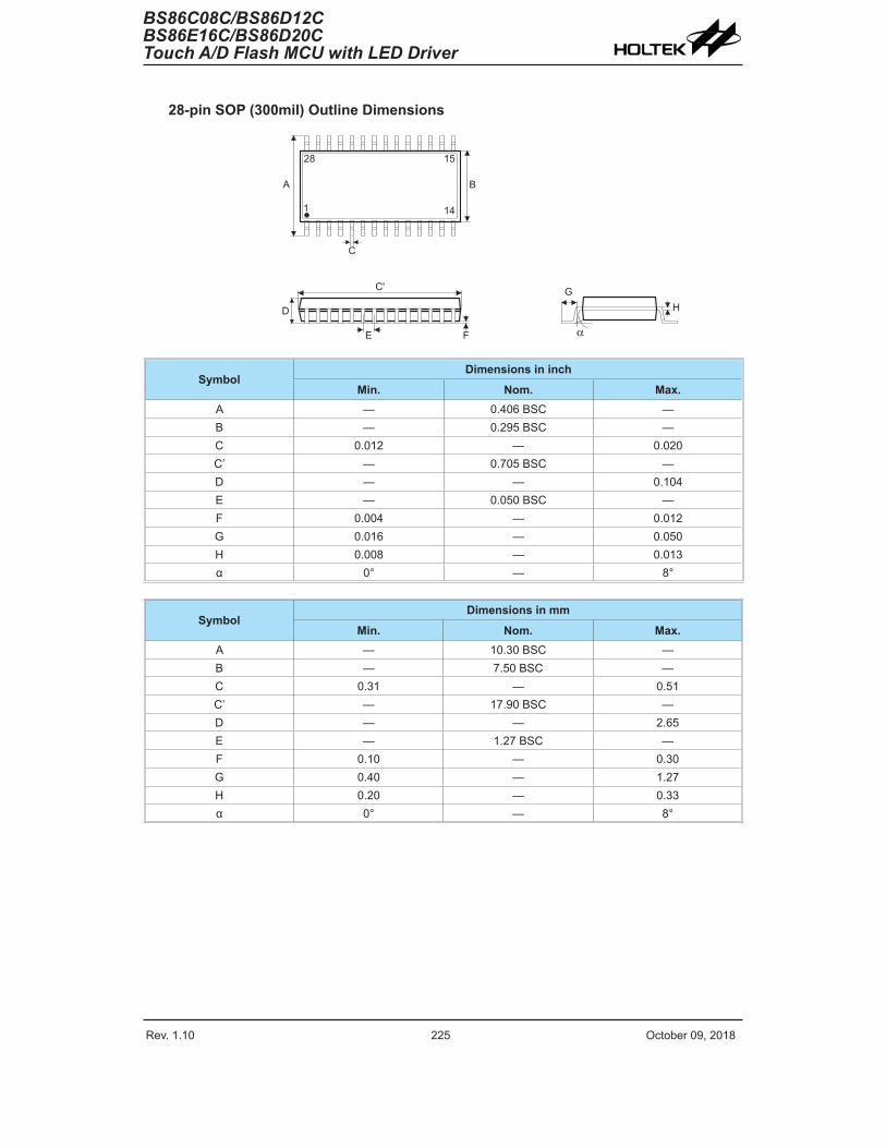
Rev. 1.10 224 October 09, 2018 Rev. 1.10 225 October 09, 2018
BS86C08C/BS86D12CBS86E16C/BS86D20C
Touch A/D Flash MCU with LED Driver
BS86C08C/BS86D12CBS86E16C/BS86D20CTouch A/D Flash MCU with LED Driver
28-pin SOP (300mil) Outline Dimensions
� �
�
� �
� �
� �
�
�
�
� � ��
��
SymbolDimensions in inch
Min. Nom. Max.A — 0.406 BSC —B — 0.295 BSC —C 0.012 — 0.020C’ — 0.705 BSC —D — — 0.104E — 0.050 BSC —F 0.004 — 0.012G 0.016 — 0.050H 0.008 — 0.013α 0° — 8°
SymbolDimensions in mm
Min. Nom. Max.A — 10.30 BSC —B — 7.50 BSC —C 0.31 — 0.51C’ — 17.90 BSC —D — — 2.65E — 1.27 BSC —F 0.10 — 0.30G 0.40 — 1.27H 0.20 — 0.33α 0° — 8°

Rev. 1.10 226 October 09, 2018 Rev. 1.10 227 October 09, 2018
BS86C08C/BS86D12CBS86E16C/BS86D20C
Touch A/D Flash MCU with LED Driver
BS86C08C/BS86D12CBS86E16C/BS86D20CTouch A/D Flash MCU with LED Driver
28-pin SSOP (150mil) Outline Dimensions
� �
�
� �
� �
� �
�
�
�
� � ��
��
SymbolDimensions in inch
Min. Nom. Max.A — 0.236 BSC —B — 0.154 BSC —C 0.008 — 0.012C’ — 0.390 BSC —D — — 0.069E — 0.025 BSC —F 0.004 — 0.010G 0.016 — 0.050H 0.004 — 0.010α 0° — 8°
SymbolDimensions in mm
Min. Nom. Max.A — 6.00 BSC —B — 3.90 BSC —C 0.20 — 0.30C’ — 9.90 BSC —D — — 1.75E — 0.635 BSC —F 0.10 — 0.25G 0.41 — 1.27H 0.10 — 0.25α 0° — 8°

Rev. 1.10 226 October 09, 2018 Rev. 1.10 227 October 09, 2018
BS86C08C/BS86D12CBS86E16C/BS86D20C
Touch A/D Flash MCU with LED Driver
BS86C08C/BS86D12CBS86E16C/BS86D20CTouch A/D Flash MCU with LED Driver
44-pin LQFP (10mm×10mm) (FP2.0mm) Outline Dimensions
� �
� ��
� �
� �
� �
� �
�
�
��
�
�
� �
� � � �
��
SymbolDimensions in inch
Min. Nom. Max.A — 0.472 BSC —B — 0.394 BSC —C — 0.472 BSC —D — 0.394 BSC —E — 0.032 BSC —F 0.012 0.015 0.018G 0.053 0.055 0.057H — — 0.063I 0.002 — 0.006J 0.018 0.024 0.030K 0.004 — 0.008α 0° — 7°
SymbolDimensions in mm
Min. Nom. Max.A — 12.00 BSC —B — 10.00 BSC —C — 12.00 BSC —D — 10.00 BSC —E — 0.80 BSC —F 0.30 0.37 0.45G 1.35 1.40 1.45H — — 1.60I 0.05 — 0.15J 0.45 0.60 0.75K 0.09 — 0.20α 0° — 7°

Rev. 1.10 228 October 09, 2018 Rev. 1.10 PB October 09, 2018
BS86C08C/BS86D12CBS86E16C/BS86D20C
Touch A/D Flash MCU with LED Driver
BS86C08C/BS86D12CBS86E16C/BS86D20CTouch A/D Flash MCU with LED Driver
Copyright© 2018 by HOLTEK SEMICONDUCTOR INC.
The information appearing in this Data Sheet is believed to be accurate at the time of publication. However, Holtek assumes no responsibility arising from the use of the specifications described. The applications mentioned herein are used solely for the purpose of illustration and Holtek makes no warranty or representation that such applications will be suitable without further modification, nor recommends the use of its products for application that may present a risk to human life due to malfunction or otherwise. Holtek's products are not authorized for use as critical components in life support devices or systems. Holtek reserves the right to alter its products without prior notification. For the most up-to-date information, please visit our web site at http://www.holtek.com/en/.