broadband linearized silicon modulator - nano-optics and...
TRANSCRIPT
Broadband linearized silicon modulator
Anatol Khilo,* Cheryl M. Sorace, and Franz X. Kärtner
Department of Electrical Engineering and Computer Science and Research Laboratory of Electronics, Massachusetts Institute of Technology, 77 Massachusetts Avenue, Cambridge, Massachusetts 02139, USA
Abstract: A scheme to achieve a wideband linearized silicon Mach-Zehnder (MZ) modulator is proposed. The modulator consists of a single MZ interferometer with identical reverse-biased silicon diode phase shifters in both arms, driven in a push-pull configuration. It is shown that the 3rd order nonlinearity of the modulator can be eliminated by canceling the nonlinearities from the silicon phase shifters and the MZ transfer function against each other. The 2nd order nonlinearity is simultaneously eliminated by differential detection or operation away from the quadrature point. As a result, the linearity of the proposed silicon modulator greatly exceeds the linearity of a conventional MZ modulator with ideal, linear (e.g. LiNbO3) phase shifters. The simplicity and large optical and RF bandwidth of the proposed modulator make it attractive for analog photonic applications.
©2011 Optical Society of America
OCIS codes: (130.4110) Modulators; (250.7360) Waveguide modulators; (060.5625) Radio frequency photonics; (070.1170) Analog optical signal processing; (060.2360) Fiber optics links and subsystems.
References and links
1. C. H. Cox III, Analog optical link: Theory and practice (Cambridge University Press, 2004). 2. C. Chang, ed., RF photonics technology fiber links (Cambridge University Press, 2002). 3. A. J. Seeds, and K. J. Williams, “Microwave photonics,” J. Lightwave Technol. 24(12), 4628–4641 (2006). 4. J. Capmany, and D. Novak, “Microwave photonics combines two worlds,” Nat. Photonics 1(6), 319–330 (2007). 5. R. C. Williamson, and R. D. Esman, “RF Photonics,” J. Lightwave Technol. 26(9), 1145–1153 (2008). 6. P. W. Juodawlkis, J. C. Twichell, G. E. Betts, J. J. Hargreaves, R. D. Younger, J. L. Wasserman, F. J. O’Donnell,
K. G. Ray, and R. C. Williamson, “Optically sampled analog-to-digital converters,” IEEE Trans. Microw. Theory Tech. 49(10), 1840–1853 (2001).
7. G. C. Valley, “Photonic analog-to-digital converters,” Opt. Express 15(5), 1955–1982 (2007), http://www.opticsinfobase.org/oe/abstract.cfm?URI=oe-15-5-1955.
8. R. A. Soref, “The past, present, and future of silicon photonics,” IEEE J. Sel. Top. Quantum Electron. 12(6), 1678–1687 (2006).
9. B. Jalali, and S. Fathpour, “Silicon photonics,” J. Lightwave Technol. 24(12), 4600–4615 (2006). 10. G. T. Reed, G. Mashanovich, F. Y. Gardes, and D. J. Thomson, “Silicon optical modulators,” Nat. Photonics
4(8), 518–526 (2010). 11. B. G. Lee, A. Biberman, J. Chan, and K. Bergman, “High-performance modulators and switches for silicon
photonic networks-on-chip,” IEEE J. Sel. Top. Quantum Electron. 16(1), 6–22 (2010). 12. J. Michel, J. Liu, and L. C. Kimerling, “High-performance Ge-on-Si photodetectors,” Nat. Photonics 4(8), 527–
534 (2010). 13. W. B. Bridges, and J. H. Schaffner, “Distortion in linearized electrooptic modulators,” IEEE Trans. Microw.
Theory Tech. 43(9), 2184–2197 (1995). 14. U. V. Cummings, and W. B. Bridges, “Bandwidth of linearized electrooptic modulators,” J. Lightwave Technol.
16(8), 1482–1490 (1998). 15. R. B. Childs, and V. A. O’Byrne, “Multichannel AM video transmission using a high-power Nd:YAG laser and
linearized external modulator,” IEEE J. Sel. Areas Comm. 8(7), 1369–1376 (1990). 16. M. Nazarathy, J. Berger, A. Ley, I. Levi, and Y. Kagan, “Progress in externally modulated AM CATV
transmission systems,” J. Lightwave Technol. 11(1), 82–105 (1993). 17. G. C. Wilson, T. H. Wood, M. Gans, J. L. Zyskind, J. W. Sulhoff, J. E. Johnson, T. Tanbun-Ek, and P. A.
Morton, “Predistortion of electroabsorption modulators for analog CATV systems at 1.55 µm,” J. Lightwave Technol. 15(9), 1654–1662 (1997).
18. Y. Chiu, B. Jalali, S. Garner, and W. Steier, “Broad-band electronic linearizer for externally modulated analog fiber-optic links,” IEEE Photon. Technol. Lett. 11(1), 48–50 (1999).
19. V. Magoon, and B. Jalali, “Electronic linearization and bias control for externally modulated fiber optic link,” in IEEE Int. Microw. Photon. Meeting, Oxford, U.K., Sep. 2000, 145–147.
#140083 - $15.00 USD Received 4 Jan 2011; accepted 15 Feb 2011; published 23 Feb 2011(C) 2011 OSA 28 February 2011 / Vol. 19, No. 5 / OPTICS EXPRESS 4485

20. R. Sadhwani, and B. Jalali, “Adaptive CMOS predistortion linearizer for fiber-optic links,” J. Lightwave Technol. 21(12), 3180–3193 (2003).
21. A. Katz, W. Jemison, M. Kubak, and J. Dragone, “Improved radio over fiber performance using predistortion linearization,” in IEEE MTT-S Int. Microw. Symp. Dig., Philadelphia, PA, Jun. 2003, 1403–1406.
22. V. J. Urick, M. S. Rogge, P. F. Knapp, L. Swingen, and F. Bucholtz, “Wide-band predistortion linearization for externally modulated long-haul analog fiber-optic links,” IEEE Trans. Microw. Theory Tech. 54(4), 1458–1463 (2006).
23. S. K. Korotky, and R. M. DeRidder, “Dual parallel modulation schemes for low-distortion analog optical transmission,” IEEE J. Sel. Areas Comm. 8(7), 1377–1381 (1990).
24. J. L. Brooks, G. S. Maurer, and R. A. Becker, “Implementation and evaluation of a dual parallel linearization system for AM-SCM video transmission,” J. Lightwave Technol. 11(1), 34–41 (1993).
25. H. Skeie, and R. Johnson, “Linearization of electro-optic modulators by a cascade coupling of phase modulating electrodes,” Proc. SPIE 1583, 153–164 (1991).
26. G. Betts, “Linearized modulator for suboctave-bandpass optical analog links,” IEEE Trans. Microw. Theory Tech. 42(12), 2642–2649 (1994).
27. M. L. Farwell, Z. Q. Lin, E. Wooten, and W. S. C. Chang, “An electrooptic intensity modulator with improved linearity,” IEEE Photon. Technol. Lett. 3(9), 792–795 (1991).
28. E. Ackerman, “Broad-band linearization of a Mach-Zehnder electrooptic modulator,” IEEE Trans. Microw. Theory Tech. 47(12), 2271–2279 (1999).
29. L. M. Johnson, and H. V. Roussell, “Reduction intermodulation distortion in interferometric optical modulators,” Opt. Lett. 13(10), 928–930 (1988).
30. L. M. Johnson, and H. V. Roussell, “Linearization of an interferometric modulator at microwave frequencies by polarization mixing,” IEEE Photon. Technol. Lett. 2(11), 810–811 (1990).
31. F. Gan, and F. X. Kärtner, “High-speed silicon electrooptic modulator design,” IEEE Photon. Technol. Lett. 17(5), 1007–1009 (2005).
32. F. Y. Gardes, G. T. Reed, N. G. Emerson, and C. E. Png, “A sub-micron depletion-type photonic modulator in Silicon On Insulator,” Opt. Express 13(22), 8845–8854 (2005), http://www.opticsinfobase.org/abstract.cfm?URI=oe-13-22-8845.
33. A. Liu, L. Liao, D. Rubin, H. Nguyen, B. Ciftcioglu, Y. Chetrit, N. Izhaky, and M. Paniccia, “High-speed optical modulation based on carrier depletion in a silicon waveguide,” Opt. Express 15(2), 660–668 (2007), http://www.opticsinfobase.org/oe/abstract.cfm?URI=oe-15-2-660.
34. L. Liao, A. Liu, D. Rubin, J. Basak, Y. Chetrit, H. Nguyen, R. Cohen, N. Izhaky, and M. Paniccia, “40 Gbit/s silicon optical modulator for high-speed applications,” Electron. Lett. 43(22), 1196–1197 (2007).
35. S. J. Spector, M. W. Geis, G. R. Zhou, M. E. Grein, F. Gan, M. A. Popovic, J. U. Yoon, D. M. Lennon, E. P. Ippen, F. Z. Kärtner, and T. M. Lyszczarz, “CMOS-compatible dual-output silicon modulator for analog signal processing,” Opt. Express 16(15), 11027–11031 (2008), http://www.opticsinfobase.org/oe/abstract.cfm?URI=oe-16-15-11027.
36. M. R. Watts, D. C. Trotter, R. W. Young, and A. L. Lentine, “Ultralow power silicon microdisk modulators and switches,” in 5th IEEE International Conference on Group IV Photonics, 4–6 (2008).
37. M. R. Watts, W. A. Zortman, D. C. Trotter, R. W. Young, and A. L. Lentine, “Low-voltage, compact, depletion-mode, silicon Mach–Zehnder modulator,” IEEE J. Sel. Top. Quantum Electron. 16(1), 159–164 (2010).
38. N. N. Feng, S. Liao, D. Feng, P. Dong, D. Zheng, H. Liang, R. Shafiiha, G. Li, J. E. Cunningham, A. V. Krishnamoorthy, and M. Asghari, “High speed carrier-depletion modulators with 1.4V-cm VπL integrated on 0.25μm silicon-on-insulator waveguides,” Opt. Express 18(8), 7994–7999 (2010), http://www.opticsinfobase.org/oe/abstract.cfm?URI=oe-18-8-7994.
39. X. Zheng, J. Lexau, Y. Luo, H. Thacker, T. Pinguet, A. Mekis, G. Li, J. Shi, P. Amberg, N. Pinckney, K. Raj, R. Ho, J. E. Cunningham, and A. V. Krishnamoorthy, “Ultra-low-energy all-CMOS modulator integrated with driver,” Opt. Express 18(3), 3059–3070 (2010), http://www.opticsinfobase.org/oe/abstract.cfm?URI=oe-18-3-3059.
40. D. M. Gill, M. Rasras, K.-Y. Tu, Y.-K. Chen, A. E. White, S. S. Patel, D. Carothers, A. Pomerene, R. Kamocsai, C. Hill, and J. Beattie, “Internal bandwidth equalization in a CMOS compatible Si-ring modulator,” IEEE Photon. Technol. Lett. 21(4), 200–202 (2009).
41. Q. Xu, B. Schmidt, S. Pradhan, and M. Lipson, “Micrometre-scale silicon electro-optic modulator,” Nature 435(7040), 325–327 (2005).
42. W. M. Green, M. J. Rooks, L. Sekaric, and Y. A. Vlasov, “Ultra-compact, low RF power, 10 Gb/s silicon Mach-Zehnder modulator,” Opt. Express 15(25), 17106–17113 (2007), http://www.opticsinfobase.org/oe/abstract.cfm?URI=oe-15-25-17106.
43. Q. Xu, S. Manipatruni, B. Schmidt, J. Shakya, and M. Lipson, “12.5 Gbit/s carrier-injection-based silicon micro-ring silicon modulators,” Opt. Express 15(2), 430–436 (2007), http://www.opticsinfobase.org/oe/abstract.cfm?URI=oe-15-2-430.
44. S. Manipatruni, X. Qianfan, B. Schmidt, J. Shakya, and M. Lipson, “High speed carrier injection 18 Gb/s silicon micro-ring electro-optic modulator,” IEEE Proc. Lasers and Electro-Optics Soc. 537–538 (2007).
45. S. Manipatruni, K. Preston, L. Chen, and M. Lipson, “Ultra-low voltage, ultra-small mode volume silicon microring modulator,” Opt. Express 18(17), 18235–18242 (2010), http://www.opticsinfobase.org/oe/abstract.cfm?URI=oe-18-17-18235.
46. A. Liu, R. Jones, L. Liao, D. Samara-Rubio, D. Rubin, O. Cohen, R. Nicolaescu, and M. Paniccia, “A high-speed silicon optical modulator based on a metal-oxide-semiconductor capacitor,” Nature 427(6975), 615–618 (2004).
#140083 - $15.00 USD Received 4 Jan 2011; accepted 15 Feb 2011; published 23 Feb 2011(C) 2011 OSA 28 February 2011 / Vol. 19, No. 5 / OPTICS EXPRESS 4486

47. L. Liao, D. Samara-Rubio, M. Morse, A. Liu, D. Hodge, D. Rubin, U. Keil, and T. Franck, “High speed silicon Mach-Zehnder modulator,” Opt. Express 13(8), 3129–3135 (2005), http://www.opticsinfobase.org/oe/abstract.cfm?URI=oe-13-8-3129.
48. Y. H. Kuo, Y. K. Lee, Y. Ge, S. Ren, J. E. Roth, T. I. Kamins, D. A. B. Miller, and J. S. Harris, “Strong quantum-confined Stark effect in germanium quantum-well structures on silicon,” Nature 437(7063), 1334–1336 (2005).
49. J. E. Roth, O. Fidaner, R. K. Schaevitz, Y.-H. Kuo, T. I. Kamins, J. S. Harris, and D. A. B. Miller, “Optical modulator on silicon employing germanium quantum wells,” Opt. Express 15(9), 5851–5859 (2007), http://www.opticsinfobase.org/oe/abstract.cfm?URI=oe-15-9-5851.
50. J. Liu, M. Beals, A. Pomerene, S. Bernardis, R. Sun, J. Cheng, L. C. Kimerling, and J. Michel, “Waveguide-integrated, ultralow-energy GeSi electro-absorption modulators,” Nat. Photonics 2(7), 433–437 (2008).
51. C. C. Sorace, A. Khilo, and F. X. Kärtner, “Broadband linear silicon Mach-Zehnder modulators,” in Integrated Photonics Research (IPR), Silicon and Nanophotonics, 2010, paper IWA4.
52. Synopsys, Sentaurus Device User Guide, Z-2010.03 ed., March 2010. 53. R. Soref, and B. Bennett, “Electrooptical effects in silicon,” IEEE J. Quantum Electron. 23(1), 123–129 (1987). 54. M. Popović, “Complex-frequency leaky mode computations using PML boundary layers for dielectric resonant
structures,” in Integrated Photonics Research 2003, Washington, DC, June 17, 2003, paper ITuD4. 55. S. J. Spector, C. M. Sorace, M. W. Geis, M. E. Grein, J. U. Yoon, T. M. Lyszczarz, E. P. Ippen, and F. X.
Kärtner, “Operation and Optimization of Silicon-Diode-Based Optical Modulators,” IEEE J. Sel. Top. Quantum Electron. 16(1), 165–172 (2010).
1. Introduction
Microwave photonics is an active research area with many applications, including antenna remoting, high-definition cable TV, radio over fiber, and photonic analog-to-digital conversion [1–7]. In microwave photonics, an analog radio-frequency (RF) signal is converted into the optical domain with a modulator, processed in the optical domain using photonic devices, and then converted back to the electrical domain. Silicon photonics is an attractive platform for microwave signal processing because of potential low-cost manufacturing and direct integration with CMOS electronics, and because many high-performance devices, such as low-loss waveguides, filters, switches, modulators, and photodetectors have already been demonstrated in the silicon platform [8–12].
In microwave photonics, the RF signal is converted into the optical domain with an electro-optic modulator. This modulator needs to be high-speed, to accommodate the RF bandwidth, and sensitive, to allow low driving voltages. The modulator also needs to be linear because nonlinearities in the modulator create distortions, which often limit the performance of a microwave photonic system. Many techniques to enhance the modulator linearity have been proposed [1,2,13–30]. Most techniques can be characterized as either pre-distortion linearization, feedback linearization, or optical transfer function linearization [1,2]. Pre-distortion linearization methods [15–22] use a nonlinear circuit preceding the modulator to distort the RF signal in such a way that the overall transfer function of the pre-distorter plus the modulator is more linear than that of the modulator alone. Pre-distortion linearization is a widely used approach, and has been successfully applied to linearize MZ modulators [15,16,18–22], directional coupler modulators [16], and multiple quantum well electroabsorption modulators [17]. However, to use pre-distortion successfully, the modulator needs to be fast enough to respond to the harmonics of the fundamental signal created by the pre-distorter. This constraint effectively reduces the RF bandwidth of the system by the order of the nonlinearity that needs to be cancelled [1]. In the feedback linearization approach, some fraction of the modulator output signal is detected and compared to the original RF signal; a feedback loop then acts to bring the difference between them to zero, ensuring linear operation. The challenges with this approach are the speed of the feedback loop (which must be fast enough to track the RF signal), and the availability of broadband RF amplifiers with sufficient gain [1]. In optical linearization approaches, two or more modulators are combined to provide a transfer function which is more linear than that of the individual modulators [13,14,23–27]. The modulators can be connected in parallel [23,24] or in series [25–27]. A conceptually similar approach is to modulate signals of different wavelengths [28] or polarizations [29,30] in a single modulator and combine them afterwards to improve the system linearity. The parameters which need to be controlled to achieve linear operation can be the optical power splitting ratio between the modulators, optical power splitting ratio
#140083 - $15.00 USD Received 4 Jan 2011; accepted 15 Feb 2011; published 23 Feb 2011(C) 2011 OSA 28 February 2011 / Vol. 19, No. 5 / OPTICS EXPRESS 4487

between the arms of an individual MZ modulator, RF voltage splitting ratio between the modulators, and the bias points of the modulators. The number of parameters to be controlled is typically higher for wideband linearization (suppression of 2nd and 3rd harmonics) and lower for sub-octave linearization (suppression of 3rd harmonic only). It is common for optical linearization approaches to result in an optical power penalty because combining modulator outputs to cancel the nonlinear harmonics usually cancels some part of the fundamental as well.
Silicon modulators are a very active area of research [10,11], with multiple groups demonstrating high-performance silicon modulators based on reverse-biased diodes [31–40], forward-biased diodes [41–45], and MOS capacitors [46,47]. Recent work on silicon-germanium structures using the quantum-confined Stark effect looks very promising [48–50]. Forward biased, ring modulators 2.5μm in radius have achieved a peak-to-peak driving voltage as small as 0.15V operating at 1 Gb/s [45]. In reverse-biased silicon diode modulators, the RF bandwidth can extend up to about 30-35 GHz [34,35,40], and VπLs as small as 1 V·cm have been achieved at speeds up to 10 Gb/s [37]. To date, most studies of silicon modulators have been performed in the context of digital transmission systems, with the modulation quality evaluated using an eye diagram and metrics such as extinction ratio. To our knowledge, no study of the linearity of silicon modulation devices for analog applications has been performed. In this work, we analyze the linearity of Mach-Zehnder (MZ) silicon modulators and predict that, despite the highly nonlinear response intrinsic to silicon, it is possible to make a modulator with linearity greatly exceeding that of a conventional MZ LiNbO3 modulator. The proposed modulator configuration is very simple and does not compromise the responsivity, optical bandwidth, or RF bandwidth of the link. The concept is applicable not only to reverse-biased silicon modulators, but also to other modulators with sufficiently high nonlinearity in their phase shifters' response.
The linearized silicon modulator proposed in this work is a push-pull MZ modulator with identical, nonlinear silicon phase shifters in its two arms. Linearization is achieved by canceling the nonlinearity of the silicon phase shifter response against the nonlinearity of the sine-squared MZ transfer function [51]. In some respects, this modulator resembles the optically linearized modulators mentioned above: the modulator is linear by itself, without the help of external electrical circuits. However, this modulator is simpler than optically linearized modulators, because it is just a single MZ structure and the only two parameters to be controlled are the MZ bias phase and the diode bias voltage. In other respects, the proposed modulator resembles pre-distortion linearized modulators: the nonlinearity of a silicon phase shifter can be viewed as analogous to the nonlinearity of a pre-distorter circuit. However, in our case, the pre-distortion function is internal to the phase shifters, which not only simplifies the implementation, but also means that the modulator RF bandwidth is not compromised by linearization. More specifically, in pre-distortion linearization, the modulator must be able to respond at the harmonics of the applied RF signal, while in our case the optical signal traveling through the silicon diodes automatically captures these harmonics and the increased bandwidth requirement does not apply.
In this work, we first describe the proposed linearization concept, which is applicable to any MZ modulator with sufficiently nonlinear phase shifters, mathematically. We then apply this concept to a silicon carrier-depletion modulator and show that its linearization is possible. We study the linearity of this modulator numerically and show that it significantly outperforms a conventional MZ modulator with ideal linear phase shifters. Finally, we examine the optical bandwidth over which the linear operation can be achieved.
2. Linearization concept
This section presents a mathematical analysis of the linearity of an MZ modulator with nonlinear phase shifters. The modulator transfer function is derived, its Taylor series expansion is analyzed, and it is shown that the 2nd and the 3rd expansion terms can be eliminated with the proper choice of modulator parameters.
#140083 - $15.00 USD Received 4 Jan 2011; accepted 15 Feb 2011; published 23 Feb 2011(C) 2011 OSA 28 February 2011 / Vol. 19, No. 5 / OPTICS EXPRESS 4488

A schematic of the MZ modulator considered in this work is shown in Fig. 1. The two arms of the MZ structure have phase shifters which are identical and described by nonlinear
voltage-dependent phase ( )v and loss ( )v . The same DC bias voltage DCv is applied to the
two arms. The RF signal ( )v v t is applied in a push-pull configuration, so that the total
voltage at the top and bottom phase shifters is DCv v and
DCv v , respectively. The optical
power at the top and the bottom outputs of the modulator can be shown to be:
2
2exp sin exp exp ,2 4 2 4 2 2
inA B A B A B
A in
PP P
(1)
2
2exp cos exp exp ,2 4 2 4 2 2
inA B A B A B
B in
PP P
(2)
where ( )A DCv v and ( )A DCv v are the phase shift and loss in the top phase
shifter, ( )B DCv v and ( )B DCv v are the phase shift and loss in bottom phase
shifter, and inP is the input power. The MZ modulator is assumed to be biased at quadrature,
so that the phase shift between the two arms at 0v is / 2 .
φ , α
φ , α
A A
B B
2vDC
v - v(t)DC
P P
P
A
B
in
0
90oφ , α
φ , α
A A
B B
2vDC
v - v(t)DC
P P
P
A
B
in
0
90o
Fig. 1. The configuration of the MZ modulator studied in this work. The two arms have identical nonlinear phase shifters biased with DC bias voltage νDC, driven in a push-pull mode with the RF signal ν(t). The 90° phase shifter biases the MZ modulator at quadrature; it will be shown that biasing the modulator slightly away from the quadrature point is one of the ways to improve the linearity.
To analyze the linearity of the MZ transfer function, let us expand the phase and loss
into a Taylor series around the DC voltage DCv :
2 3
1 2 3 ,DC DCv v v v v L (3)
2 3
1 2 3 ,DC DCv v v v v L (4)
where L is the length of the phase shifters. Note that according to Eqs. (1) and (2), the output
powers depend not on individual phases A and
B , but rather on the phase difference
A B . Using expansion (3), this phase difference is
3
1 3( ) ( ) 2 .A B DC DCv v v v v v L (5)
The second and higher-order even terms of the phase response expansion are automatically cancelled in Eq. (5) thanks to the symmetry of the push-pull configuration. In the case of a reverse-biased silicon diode, the second-order phase nonlinearity is the dominant nonlinear term, and its cancellation due to the push-pull symmetry is critical for wideband linearization.
#140083 - $15.00 USD Received 4 Jan 2011; accepted 15 Feb 2011; published 23 Feb 2011(C) 2011 OSA 28 February 2011 / Vol. 19, No. 5 / OPTICS EXPRESS 4489

Plugging Eqs. (3)–(5) into Eqs. (1) and (2) and performing a Taylor expansion, the expressions that describe modulator linearity are finally obtained:
2 2 2 3 3 2 3
1 1 2 1 3 1 2
1 22 ,
2 3DC L
A inP P e L v L L v L L L v
(6)
2 2 2 3 3 2 3
1 1 2 1 3 1 2
1 22 .
2 3DC L
B inP P e L v L L v L L L v
(7)
The above equations can be analyzed as follows. The third-order nonlinear coefficient is the sum of three terms: (i) the term due to the cubic nonlinearity of the sine-squared MZ transfer function, which is present even in the case of ideal linear phase shifters; (ii) the term due to the cubic nonlinearity of the phase shifters; and (iii) the term due to the quadratic nonlinearity of the loss in the phase shifters. If these terms can be made to cancel each other, the third order nonlinear coefficient can be set to zero. Demanding such cancellation yields a quadratic equation in L:
3 2
1 1 2 3
22 0.
3L L (8)
Linearization is possible only if this equation has real, positive solutions for the phase shifter length, L. Additionally, L must be long enough for high modulation depth to be possible, but short enough that the modulator does not take up too much chip area. Whether an acceptable length is possible depends on the above coefficients, which are determined by the shapes of
the phase shifter response curves ( )v and ( )v , as well as by the selected bias voltage DCv .
In the next section, it will be shown that a reverse-biased silicon diode phase shifter has nonlinearity suitable for the cancellation of the cubic nonlinear term in the transfer function at practical diode lengths.
The modulator transfer function also has second-order nonlinearity, see Eqs. (6) and (7), from the voltage-dependent loss. The quadratic nonlinearity is not a problem in systems with sub-octave bandwidth. However, wideband systems, such as photonic analog-to-digital converters, are affected by quadratic nonlinearity, and suppression of the second-order nonlinear term is highly desirable. The two terms of the second-order nonlinear coefficient can, in principle, cancel each other. However, this cancellation is of limited usefulness because it occurs at a different phase-shifter length than the cancellation of the cubic nonlinearity. There are two approaches to eliminating the quadratic nonlinearity without compromising the cancellation of the cubic nonlinear term. The first approach is to use differential detection: according to Eqs. (6) and (7), the second order nonlinear terms in the complimentary outputs are identical, so subtracting these outputs will eliminate the second order nonlinearity (as well as all other even-order nonlinearities). Because the odd nonlinearities have opposite signs in the two outputs, such subtraction will not eliminate the desired, linear term. The second approach is to shift the operating point of the MZ modulator away from quadrature to introduce a quadratic term in the sine-square MZ transfer function. At the proper operating point, this quadratic term will cancel the quadratic term of Eq. (6) or (7) and result in MZ modulator operation free of quadratic nonlinearity. A similar analysis to the one above, where the operating point was allowed to change, shows that cancellation of the 3rd order nonlinearity occurs at the same length regardless of operating point. Therefore, the cancellation of the 3rd order nonlinearity is not affected when the operating point is changed to cancel the 2nd order nonlinearity, and simultaneous cancellation of 2nd and 3rd order nonlinearities is straightforward. Note that this approach can eliminate quadratic nonlinearity only in one of the two modulator outputs, which is often sufficient because many applications use only a single output.
#140083 - $15.00 USD Received 4 Jan 2011; accepted 15 Feb 2011; published 23 Feb 2011(C) 2011 OSA 28 February 2011 / Vol. 19, No. 5 / OPTICS EXPRESS 4490

Once the 3rd-order and all even order nonlinear terms of the modulator transfer function are eliminated, as described above, the modulator linearity will be limited by the 5th and higher-order odd nonlinear terms. Table 1 summarizes the results of this section.
Table 1. Different Nonlinear Terms and the Ways to Cancel Them as Described in Section 2
Nonlinear term Source of nonlinearity Method of cancellation
2nd and other even-order terms
quadratic and other even-order nonlinearity of φ(v)
Cancelled due to push-pull symmetry.
2nd and other even-order terms
linear, quadratic, and other nonlinear terms of α(v)
Cancelled by using differential detection.
2nd-order term linear and quadratic terms of α(v)
Cancelled (in one of the two outputs) by shifting the operating point away from quadrature.
3rd order term cubic term of φ(v) + cubic term of MZ transfer function + quadratic term of α(v)
Eliminated with proper choice of phase shifter length. At this length, different contributions to the cubic nonlinearity cancel each other.
5th order term In general, cannot be cancelled simultaneously with the 3rd order term. Limits the linearity of the linearized modulator.
3. Linearization of a reverse-biased silicon modulator
The theoretical analysis presented above shows that the transfer function of an MZ modulator with nonlinear phase shifters can be linearized with the proper choice of modulator
parameters, provided that the phase shifters have a suitable nonlinear phase ( )v and loss
( )v response. While the linearization is not necessarily achievable for arbitrary phase shifter
nonlinearity, this section shows that a reverse-biased silicon diode phase shifter has the right amount of nonlinearity to enable linearization. The performance of such a linearized silicon modulator is analyzed and compared to a conventional MZ modulator.
A reverse-biased silicon modulator uses the free carrier plasma dispersion effect to modulate the optical signal. The RF voltage applied to a reverse-biased diode changes the width of the depletion region and, thus, the free carrier concentration profile within the diode. The optical mode traveling through the diode experiences a phase shift induced by these free carriers. The MZ structure serves to turn this phase modulation into an amplitude modulation. Free carriers induce not only a phase shift, but also undesired absorption, which needs to be included in the linearity analysis.
Before proceeding to a rigorous treatment of silicon modulators, rough estimates can be used to illustrate the possibility of canceling the cubic nonlinear term. The quadratic Eq. (8) derived in the previous section can be simplified by neglecting the term related to the voltage-
induced loss. Equation (8) becomes 3 2
1 3
20
3L . A positive solution for L is possible only
if the phase nonlinear coefficients, 1 and
3 , have the same sign. To verify that this is the
case for a reverse-biased silicon diode, we can use the Shockley diode model. In this mode, the width of the depletion region is proportional to the square root of the applied voltage,
DCv v . The induced change in the effective index of the optical mode is approximately
proportional to the width of the depletion zone, therefore ( ) ~ DCv v v . Taylor series
expansion gives
2 3
1 1 1( ) ~ 1 ... .
2 8 16DC
DC DC DC
v v vv v
v v v
(9)
The nonlinear coefficients, 1 and
3 , indeed have the same sign. Therefore, this modulator
can be linearized, i.e. it is always possible to find a positive length L at which the cubic
#140083 - $15.00 USD Received 4 Jan 2011; accepted 15 Feb 2011; published 23 Feb 2011(C) 2011 OSA 28 February 2011 / Vol. 19, No. 5 / OPTICS EXPRESS 4491

nonlinearity of the MZ transfer function 3 3
1 L cancels the cubic nonlinearity of the phase
shifters 3L .
Though a description based on Shockley's diode model gives a qualitative picture of modulator linearization, it is not accurate enough for quantitative analysis. In this work,
rigorous numerical simulations were used to find the shapes of the ( )v and ( )v curves for
a reverse-biased silicon diode. Electrical simulations were performed in Synopsys's Sentaurus
® software suite [52] and determined the spatial carrier concentration distribution as
a function of applied voltage. The electrical model used to find the carrier distributions included mobility, recombination, bandgap and breakdown effects. The carrier concentrations were then converted into refractive index and absorption coefficient distributions [53]. Finally, the obtained index and absorption distributions were substituted into a vectorial mode solver [54] to determine the effective index and attenuation coefficient of the optical mode.
The designs of a reverse-biased silicon diode can be different in terms of waveguide cross-sections and doping profiles. To be specific, we selected the diode design shown in Fig. 2 [55] and used it in the rest of this work. This design was optimized solely to maximize the diode responsivity, without consideration to the diode nonlinear characteristics. The calculated
phase and loss response, ( )v and ( )v , per unit length of the diode phase shifter are shown
in Fig. 3. Note that in Fig. 3, and throughout this work, positive voltages are voltages applied in the reverse-bias direction. The wavelength of light is assumed to be fixed at 1.55μm; wavelength dependence of modulator linearity will be studied in Sec. 4.
51017 p-type
1.51018 n-type
1018 p-type
co
nta
ct
50
nm
50nm
500nm
22
0n
m
50nm
SiO2
SiO2
50nm
co
nta
ctSiO2
p++ n++51017 p-type
1.51018 n-type
1018 p-type
co
nta
ct
50
nm
50nm
500nm
22
0n
m
50nm
SiO2
SiO2
50nm
co
nta
ctSiO2
p++ n++
Fig. 2. Cross-section of the reverse-biased silicon diode phase shifter studied in this work. This diode was designed to maximize the modulator sensitivity without regards to its linearity.
Fig. 3. (a) Phase shift and (b) change in the modal loss per centimeter of a silicon diode phase shifter length versus applied voltage. The diode cross-section is shown in Fig. 2. The circles represent simulation data points, and the curves an 8th-order polynomial fit to these points. 1.55μm light is assumed.
To study the nonlinear characteristics of the modulator, the modulator transfer functions
(1-2) were generalized to allow for MZ bias values different from quadrature. The phase ( )v
#140083 - $15.00 USD Received 4 Jan 2011; accepted 15 Feb 2011; published 23 Feb 2011(C) 2011 OSA 28 February 2011 / Vol. 19, No. 5 / OPTICS EXPRESS 4492
and loss ( )v were determined by an 8-th order polynomial fit to the simulation data points
(shown in Fig. 3). The polynomial fitting provided a way to calculate the phase and loss for arbitrary voltage values. As one has to expect, it was observed that suppression of the harmonics to a level of 60dBc and below is very sensitive to noise in the numerical data, as well as the exact fitting function used, and the exact implementation of the algorithm. Fortunately, while choice of fit creates some shift in the output graphs, all qualitative results remain the same. Moreover, despite the obvious differences in curve values with fitting choice, the quantitative differences were not so great as to exclude using bias-point tuning to achieve the desired linearity, as discussed below. To study the modulator linearity, we
generated a single-tone sinusoidal input signal, ( )v t , applied to it the MZ transfer function
with ( )v and ( )v given by the polynomial fits, and analyzed the harmonic distortions of
the obtained output signal. The extent to which the silicon modulator can be linearized, and the phase shifter length at
which linear operation is achieved, can now be found. The nonlinearity of the silicon diode phase shifters depends on the bias voltage. To start, the bias voltage is chosen to be 4V; arbitrary values of the bias voltage will be considered later. Numerical simulations show that the cubic nonlinearity is completely eliminated for L = 263μm. The harmonic distortions as a function of modulation depth for this phase shifter length are shown in Fig. 4(a). The
modulation depth is defined as max/I I , where I is the intensity swing at the output of the
modulator for given RF amplitude, and maxI is the maximum possible intensity swing
corresponding to full modulation. The powers of the harmonic distortions are specified relative to the power of the fundamental. The 3rd harmonic distortion in the linearized modulator (“HD3 lin. MZM” curve) is significantly reduced compared to a conventional MZ modulator with ideal linear phase shifters (“HD3, conv. MZM” curve), especially at small modulation depths. Note that in the absence of cubic nonlinearity, HD3 originates from the 5th order nonlinearity, as confirmed by the slope of the curve. The second harmonic (“loss-induced HD2” curve) will not be present in the proposed modulator. This curve corresponds
to the second harmonic originating from the voltage-dependent loss ( )v if the modulator
were biased at quadrature. As explained in the previous section, HD2 can be completely eliminated by biasing the modulator away from the quadrature point or by using differential detection.
#140083 - $15.00 USD Received 4 Jan 2011; accepted 15 Feb 2011; published 23 Feb 2011(C) 2011 OSA 28 February 2011 / Vol. 19, No. 5 / OPTICS EXPRESS 4493

Fig. 4. Harmonic distortions in the linearized silicon modulator and a conventional MZ modulator as a function of modulation depth. The curves “HD3, lin MZM” and “HD5, lin MZM” represent the 3rd and 5th harmonic distortions in the linearized silicon modulator, and the curve “HD3, conv. MZM” is the 3rd harmonic distortion in a conventional MZ modulator with ideal, linear phase shifters. The curve “loss-induced HD2” illustrates the amount of the 2nd harmonic distortion due to voltage-dependent loss, which can be completely eliminated by shifting the MZ bias away from quadrature or by using differential detection. The length is selected (a) to completely eliminate the cubic nonlinearity, (b) to achieve the largest
modulation depth while keeping HD3 below the 80dBc level; (c) to achieve the largest
modulation depth while keeping HD3 below the 60dBc level (see Table 2). The silicon diode reverse bias voltage was 4V; see Fig. 6 for the performance at arbitrary reverse bias voltages.
The performance of the modulator with no cubic nonlinearity (Fig. 4(a)) is limited by the 5th order nonlinearity, which quickly increases with modulation depth and limits the benefit of linearization at high modulation depths. To achieve better linearity at high modulation depths, some amount of cubic nonlinearity can be allowed. The idea is to let the contributions of the cubic and the 5th order nonlinearity to the HD3 cancel at some signal power, thus, yielding a more linear performance at this power. Figure 4(b) illustrates this concept. Here,
the phase shifter length (L = 280μm) is optimized in order to keep the HD3 below the 80dBc level up to highest possible modulation depth. The modulation depth at which the HD3 first
crosses the 80dBc level is increased from 18% (Fig. 4(a)) to 30%, i.e. the HD3 stays below
80dBc for all modulation depths lower than 30%. This increase comes at the expense of higher distortion at lower modulations depths. However, since distortions are small at low modulations depths, generally, their increase is not problematic. In Fig. 4(c), the length, L = 312μm, was optimized to achieve the highest possible modulation depth where the HD3 was
suppressed below 60dBc. Compared to the fully cancelled cubic nonlinearity (Fig. 4(a)), the acceptable modulation depth increased from 32% to 68%. A conventional MZ modulator
allows only 15% modulation with HD3 below 60dBc. We will continue to consider these three linearization criteria; for convenience, they are summarized in Table 2.
Table 2. Three Criteria for Modulator Linearization Considered in Section 3
No. Criterion Explanation 1 Fully cancelled
cubic nonlinearity The cubic nonlinear term of the modulator transfer function is completely eliminated. (Fig. 4(a))
2 80dBc level optimization
The modulator is optimized to maximize the modulation depth up to which the
third harmonic distortion, HD3, stays below the 80dBc level. (Fig. 4(b)) 3 60dBc level
optimization Same as above but with the HD3 below the 60dBc level. (Fig. 4(c))
The above discussion assumed a diode bias of 4V; the analysis will now be extended to arbitrary bias voltages. The three linearization criteria listed in Table 2 are again considered. The lengths of the phase shifters which yield the most linear performance as a function of bias
#140083 - $15.00 USD Received 4 Jan 2011; accepted 15 Feb 2011; published 23 Feb 2011(C) 2011 OSA 28 February 2011 / Vol. 19, No. 5 / OPTICS EXPRESS 4494
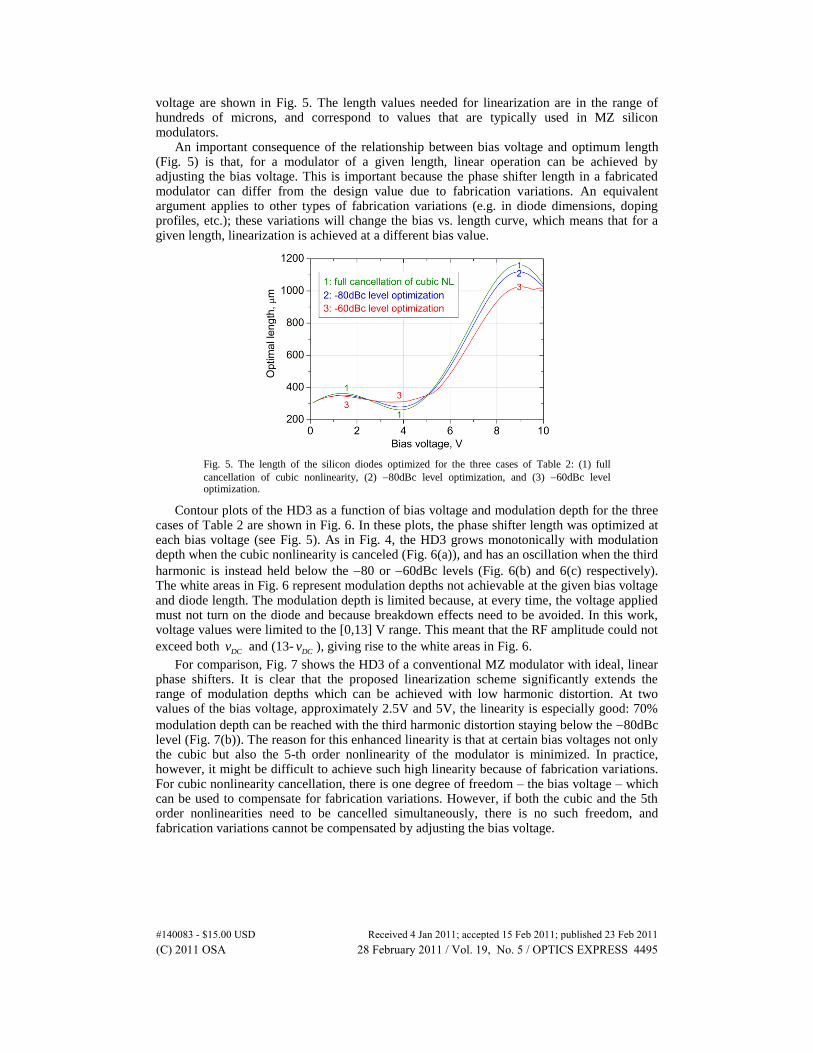
voltage are shown in Fig. 5. The length values needed for linearization are in the range of hundreds of microns, and correspond to values that are typically used in MZ silicon modulators.
An important consequence of the relationship between bias voltage and optimum length (Fig. 5) is that, for a modulator of a given length, linear operation can be achieved by adjusting the bias voltage. This is important because the phase shifter length in a fabricated modulator can differ from the design value due to fabrication variations. An equivalent argument applies to other types of fabrication variations (e.g. in diode dimensions, doping profiles, etc.); these variations will change the bias vs. length curve, which means that for a given length, linearization is achieved at a different bias value.
Fig. 5. The length of the silicon diodes optimized for the three cases of Table 2: (1) full
cancellation of cubic nonlinearity, (2) 80dBc level optimization, and (3) 60dBc level optimization.
Contour plots of the HD3 as a function of bias voltage and modulation depth for the three cases of Table 2 are shown in Fig. 6. In these plots, the phase shifter length was optimized at each bias voltage (see Fig. 5). As in Fig. 4, the HD3 grows monotonically with modulation depth when the cubic nonlinearity is canceled (Fig. 6(a)), and has an oscillation when the third
harmonic is instead held below the 80 or 60dBc levels (Fig. 6(b) and 6(c) respectively). The white areas in Fig. 6 represent modulation depths not achievable at the given bias voltage and diode length. The modulation depth is limited because, at every time, the voltage applied must not turn on the diode and because breakdown effects need to be avoided. In this work, voltage values were limited to the [0,13] V range. This meant that the RF amplitude could not
exceed both DCv and (13-
DCv ), giving rise to the white areas in Fig. 6.
For comparison, Fig. 7 shows the HD3 of a conventional MZ modulator with ideal, linear phase shifters. It is clear that the proposed linearization scheme significantly extends the range of modulation depths which can be achieved with low harmonic distortion. At two values of the bias voltage, approximately 2.5V and 5V, the linearity is especially good: 70%
modulation depth can be reached with the third harmonic distortion staying below the 80dBc level (Fig. 7(b)). The reason for this enhanced linearity is that at certain bias voltages not only the cubic but also the 5-th order nonlinearity of the modulator is minimized. In practice, however, it might be difficult to achieve such high linearity because of fabrication variations. For cubic nonlinearity cancellation, there is one degree of freedom – the bias voltage – which can be used to compensate for fabrication variations. However, if both the cubic and the 5th order nonlinearities need to be cancelled simultaneously, there is no such freedom, and fabrication variations cannot be compensated by adjusting the bias voltage.
#140083 - $15.00 USD Received 4 Jan 2011; accepted 15 Feb 2011; published 23 Feb 2011(C) 2011 OSA 28 February 2011 / Vol. 19, No. 5 / OPTICS EXPRESS 4495

405
0607
08090
100
130
130
130
100
90 80 60
100 90 80 70 60 50
40
(a) full cancellation of
cubic nonlinearity70
100
130
70
40
50607080
5060809090
13
0
100
9013
0
100
7080
90
(b) -80dBc level
optimization
(c) -60dBc level
optimization
70
8090
100
40
7080
90100
130
100 70
506070
70
90 80
60
70
405
0607
08090
100
130
130
130
100
90 80 60
100 90 80 70 60 50
40
(a) full cancellation of
cubic nonlinearity70
100
130
70
40
50607080
5060809090
13
0
100
9013
0
100
7080
90
(b) -80dBc level
optimization
(c) -60dBc level
optimization
70
8090
100
40
7080
90100
130
100 70
506070
70
90 80
60
70
405
0607
08090
100
130
130
130
100
90 80 60
100 90 80 70 60 50
40
(a) full cancellation of
cubic nonlinearity70
405
0607
08090
100
130
130
130
100
90 80 60
100 90 80 70 60 50
40
(a) full cancellation of
cubic nonlinearity70
100
130
70
40
50607080
5060809090
13
0
100
9013
0
100
7080
90
(b) -80dBc level
optimization
70
40
50607080
5060809090
13
0
100
9013
0
100
7080
90
(b) -80dBc level
optimization
(c) -60dBc level
optimization
70
8090
100
40
7080
90100
130
100 70
506070
70
90 80
60
70
Fig. 6. Third harmonic distortion, HD3, in dBc, as a function of the silicon diode bias voltage and modulation depth. At each bias voltage, the length of the silicon diode was optimized (shown in Fig. 5). Three criteria of length optimization have been used (see Table 2): (a) full cancellation of the cubic nonlinearity, (b) maximization of the modulation depth with HD3
below the 80dBc level, (c) maximization of the modulation depth with HD3 below the
60dBc level. The white areas in the plots correspond to modulation depths not achievable at given phase shifter length and bias voltage. For comparison, a plot of the HD3 in a conventional MZ modulator with ideal, linear phase shifters is shown in Fig. 7 (see also the curves labeled “HD3, conv. MZM” in Fig. 4). Note that the minus sign in front of the HD3 values has been omitted; in reality, the HD3 is, of course, negative.
#140083 - $15.00 USD Received 4 Jan 2011; accepted 15 Feb 2011; published 23 Feb 2011(C) 2011 OSA 28 February 2011 / Vol. 19, No. 5 / OPTICS EXPRESS 4496

30
40
50
60
70
80
100
90
20
30
40
50
60
70
80
100
90
20
Fig. 7. Third harmonic distortion, HD3, in dBc, present in a conventional MZ modulator with ideal linear (e.g. LiNbO3) phase shifters. The minus sign in front of the HD3 values has been omitted.
4. Optical bandwidth of the linearized, silicon modulator
Until now, the optimization and analysis of the modulator linearity was performed for a single optical wavelength. However, in many applications, modulators must be able to operate over a wide wavelength range. For example, in an optical ADC, the optical bandwidth of the pulse train input to the modulator can be 20nm or more. This section addresses the wavelength dependence of the modulator linearity.
In Sec. 2, it was established that the cubic nonlinearity of the modulator is fully cancelled when the length of its phase shifter sections satisfies Eq. (8). However, the optical phase shift depends on wavelength, which means that the optimum length also depends on wavelength. The cubic nonlinearity in a given modulator can be zero only at a single wavelength; it will increase as the wavelength differs from this wavelength. This is illustrated in Fig. 8, which shows the third harmonic distortion, HD3, as a function of wavelength for a modulator optimized at 1.55μm. The HD3 shown is the maximum HD3 over modulation depths ranging from 0 to 20% (rather just the HD3 at 20% depth). The bias voltage was 2V and the length was 348μm. One can see that HD3 grows rather quickly with distance from 1.55μm: HD3 increases by about 10dB just 3nm away from 1.55μm. However, there is still bandwidth over
which HD3 remains low. For example, HD3 remains below 100dBc within a 9nm
bandwidth, and below 90dB within a 29nm bandwidth around 1.55μm, as indicated in Fig. 8. The bandwidth can therefore be plotted as a function of the HD3 level, as it is done in Fig. 9.
Fig. 8. Maximum third harmonic distortion, HD3, with up to 20% modulation depth as a function of optical wavelength. The length was L = 348μm, selected to minimize HD3 at 1.55μm. The bias voltage was 2V. For comparison, HD3 in a modulator with ideally linear
phase shifters at 20% modulation depth is 55dBc.
Figure 9 shows how much suppression of nonlinear distortions can be achieved over a given bandwidth. The Y-axis is the bandwidth over which the HD3 stays below the level
#140083 - $15.00 USD Received 4 Jan 2011; accepted 15 Feb 2011; published 23 Feb 2011(C) 2011 OSA 28 February 2011 / Vol. 19, No. 5 / OPTICS EXPRESS 4497
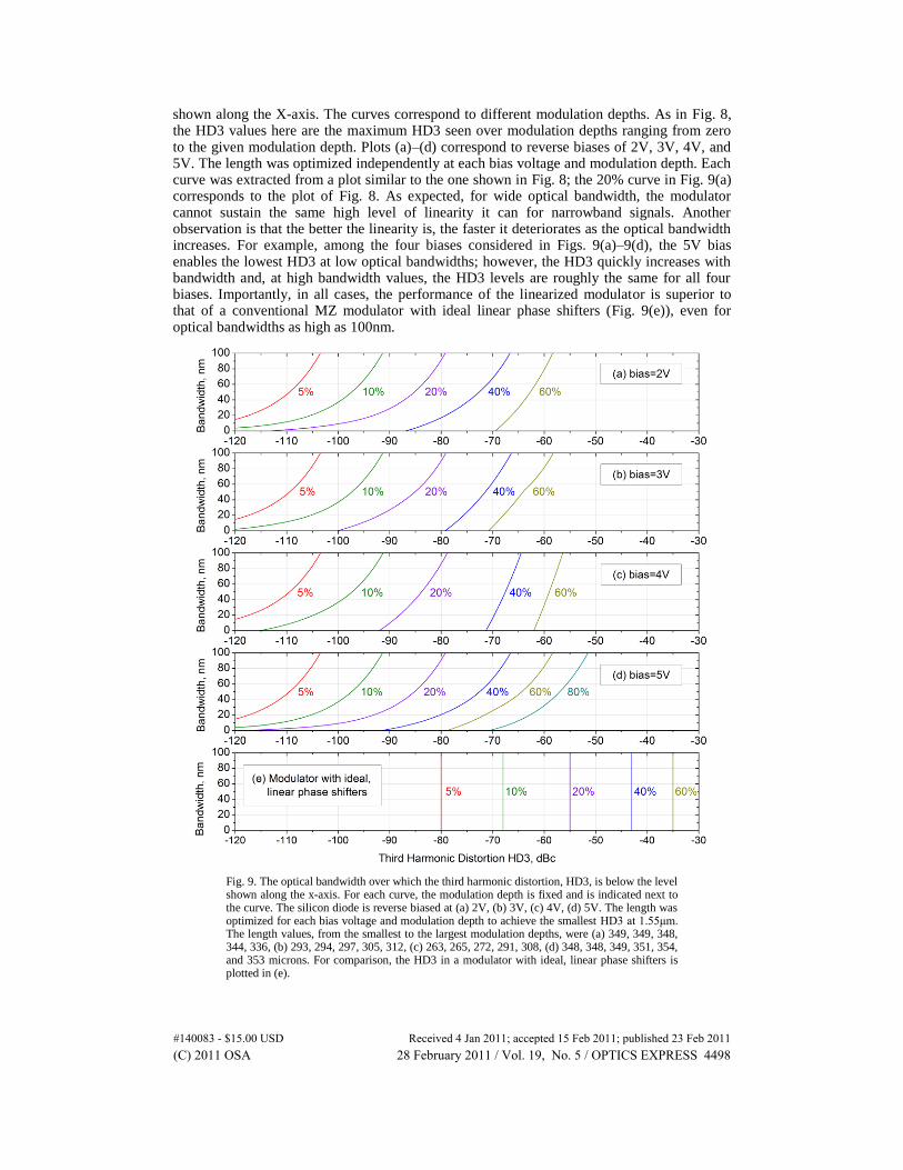
shown along the X-axis. The curves correspond to different modulation depths. As in Fig. 8, the HD3 values here are the maximum HD3 seen over modulation depths ranging from zero to the given modulation depth. Plots (a)–(d) correspond to reverse biases of 2V, 3V, 4V, and 5V. The length was optimized independently at each bias voltage and modulation depth. Each curve was extracted from a plot similar to the one shown in Fig. 8; the 20% curve in Fig. 9(a) corresponds to the plot of Fig. 8. As expected, for wide optical bandwidth, the modulator cannot sustain the same high level of linearity it can for narrowband signals. Another observation is that the better the linearity is, the faster it deteriorates as the optical bandwidth increases. For example, among the four biases considered in Figs. 9(a)–9(d), the 5V bias enables the lowest HD3 at low optical bandwidths; however, the HD3 quickly increases with bandwidth and, at high bandwidth values, the HD3 levels are roughly the same for all four biases. Importantly, in all cases, the performance of the linearized modulator is superior to that of a conventional MZ modulator with ideal linear phase shifters (Fig. 9(e)), even for optical bandwidths as high as 100nm.
Fig. 9. The optical bandwidth over which the third harmonic distortion, HD3, is below the level shown along the x-axis. For each curve, the modulation depth is fixed and is indicated next to the curve. The silicon diode is reverse biased at (a) 2V, (b) 3V, (c) 4V, (d) 5V. The length was optimized for each bias voltage and modulation depth to achieve the smallest HD3 at 1.55μm. The length values, from the smallest to the largest modulation depths, were (a) 349, 349, 348, 344, 336, (b) 293, 294, 297, 305, 312, (c) 263, 265, 272, 291, 308, (d) 348, 348, 349, 351, 354, and 353 microns. For comparison, the HD3 in a modulator with ideal, linear phase shifters is plotted in (e).
#140083 - $15.00 USD Received 4 Jan 2011; accepted 15 Feb 2011; published 23 Feb 2011(C) 2011 OSA 28 February 2011 / Vol. 19, No. 5 / OPTICS EXPRESS 4498
Note that the analysis in this section assumes that the only source of wavelength dependence in a silicon MZ modulator is the wavelength dependence of the phase and loss in the silicon diode phase shifters. However, other parameters of the MZ structure can also be wavelength-dependent and, thus, can affect modulator linearity for wideband optical inputs. In particular, the coupling ratio of the directional couplers and the bias phase of the modulator can vary with wavelength. The impact of these variations was not considered because they are not fundamental to the proposed linearization method and will affect the performance of any MZ-based modulator.
5. Summary and discussion
This work describes a modulator linearization scheme based on cancellation between the phase shifter and the MZ transfer function nonlinearities. This concept is applicable to any modulator with nonlinear phase shifters, including the reverse-biased silicon diode phase shifters studied in this work. The silicon phase shifters are intrinsically nonlinear, with both phase and loss dependent on the applied voltage in a nonlinear way. That nonlinearity allows overall linear operation to be achieved in the MZ structure at reasonable device operating voltages and lengths. The linearized modulator yields superior linearity to a conventional MZ modulator with ideal linear phase shifters, as illustrated by Figs. 4, 6, 7, and 9. For example, if
the third harmonic distortion HD3 needs to be below 80dBc, a conventional MZ modulator is limited to 5% modulation depth, while the linearized silicon modulator considered in this work enables 30% modulation at a 4V bias voltage and 57% modulation at a 5V bias voltage. The linearity of the modulator depends on the optical wavelength, i.e. a modulator optimized for one wavelength will not perform equally well at other wavelengths. In the above example,
if the HD3 is additionally required to be below 80dBc over 100nm of optical bandwidth, the modulation depth in the linearized modulator is reduced to about 20% at both bias voltages, which is still higher than in the conventional MZ case.
As mentioned in the Introduction, the proposed linearization method resembles the pre-distortion linearization in the sense that the nonlinearity of the phase shifters is conceptually similar to the nonlinearity introduced with a pre-distorter circuit. Unlike pre-distortion linearization methods, the proposed scheme does not require the modulator to work at harmonics of the applied RF signal, and, therefore, does not compromise the RF bandwidth of the modulator. However, operation at high RF frequencies may still be degraded by possible dynamic nonlinearity, i.e. the dependence of nonlinearity of the silicon phase shifter on the RF frequency. This work does not address the question about the presence and impact of this dynamic nonlinearity on the linearity of the modulator.
As with any linearization approach which relies on nonlinearity cancellation, an important question is the tolerance of the proposed approach to device parameter variations. Specifically, the diode parameters such as layer thicknesses, doping levels, and spatial doping profiles can vary from one fabrication run to another and from diode to diode in the same fabrication run, leading to variations in the nonlinearity in the phase shifters. Because the phase shifter nonlinearity also depends on an adjustable parameter – the diode bias voltage – some variations in phase shifter linearity can be compensated by simply adjusting this voltage. This is particularly true if both arms are still balanced. Fabrication variations can also lead to unbalanced arms, and while it is expected that the proximity of the two diodes on the chip will keep these variations low, the question about their impact on the modulator linearization remains open. Note that fabrication variations might be problematic if one’s goal is to achieve the very high linearity associated with simultaneous suppression of the 3rd and 5th order nonlinear terms, which only happens at specific combinations of modulator parameters and bias voltage.
Note that the modulator linearity was studied by analyzing the harmonic distortions created when a single-frequency RF tone is applied to the modulator. A single-tone test was selected for simplicity; a two-tone test could be used instead and intermodulation distortions could be analyzed. The intermodulation distortion analysis would produce different absolute values of distortions, but it would not change the relationship between the distortions in a
#140083 - $15.00 USD Received 4 Jan 2011; accepted 15 Feb 2011; published 23 Feb 2011(C) 2011 OSA 28 February 2011 / Vol. 19, No. 5 / OPTICS EXPRESS 4499

linearized and a conventional modulator. Therefore, all conclusions of this work would stay the same.
In this work, the modulator linearity is analyzed theoretically, using models and numerical simulations. However, the theory might be different from the experiment for a number of reasons. First, the parameters of a fabricated device might be different from the intended values. Second, some of the diode parameters used in the models might not be very well known; for example, the exact doping profiles. Third, although the authors used rigorous models to find the carrier distributions at given voltages, these models are still approximate: they assume there are no defects in the silicon, that the contacts are perfectly ohmic, use standard, empirical models for physical parameters like temperature and carrier concentration effects on the bandgap and on index of refraction and loss, etc. For these reasons, differences between the real nonlinearity of the fabricated device and the nonlinearity predicted by the model are unavoidable. Therefore, to make a linearized modulator in a given fabrication process, one needs to establish the nonlinearity of the silicon phase shifters experimentally. The simulation results, such as the results presented in the paper, should be viewed as a guide to the performance expected of a properly linearized silicon modulator and an estimation of the parameters necessary for linearization.
Acknowledgements
This work was sponsored by the Defense Advanced Research Projects Agency EPIC Program under contract W911NF-04-1-0431. Cheryl Sorace would like to acknowledge support from an National Science Foundation GRF.
#140083 - $15.00 USD Received 4 Jan 2011; accepted 15 Feb 2011; published 23 Feb 2011(C) 2011 OSA 28 February 2011 / Vol. 19, No. 5 / OPTICS EXPRESS 4500