bringing nanotechnology into fiber opticsfiber optics … · bringing nanotechnology into fiber...
TRANSCRIPT
Bringing Nanotechnology into Fiber Opticsinto Fiber Optics
Prof. Maksim Skorobogatiy
www.photonics.phys.polymtl.ca
Canada Research Chair in Micro and Nano PhotonicsÉ l P l h i d M é lÉcole Polytechnique de Montréalwww.photonics.phys.polymtl.ca
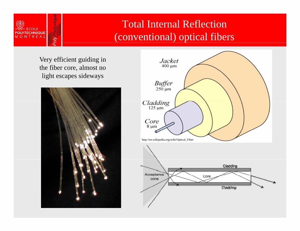
Total Internal Reflection (conventional) optical fibers
Very efficient guiding in the fiber core, almost no light escapes sideways
http://en.wikipedia.org/wiki/Optical_Fiber
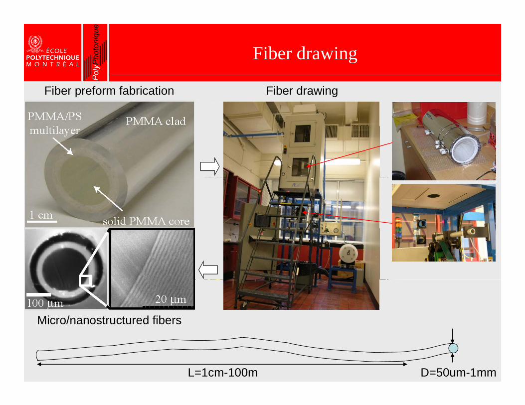
Fiber drawing
Fiber drawingFiber preform fabrication
Micro/nanostructured fibers
D=50um-1mmL=1cm-100m

Applications of fiber optics beyond telecommunications
Mechanically flexible technology for large area illumination, distributed sensing,
information transmission and fashioninformation transmission, and fashion
Photonic textiles enable
Illumination1. Practically unlimited coverage area and complex shapes2. Apparel with unusual or/and dynamically addressable appearance 3 Fiber based illuminators can be used not only in the visible ( 500nm) but also in the IR3. Fiber-based illuminators can be used not only in the visible (~500nm) but also in the IR
(invisible) ranges (1-10μm) for security and military applications
Sensing (optical fiber-based)1. Distributed sensing (T, P, …) over 1m-1km X 1m-1km areas without any point sensors2. Electrically passive technology, ability to operate in flammable environment3. Textiles can be easily integrated into large scale structures such as bridges, houses, etc. for
long term structural integrity monitoring with minimal servicing requirements.g g y g g q
Communication1. Integration of the fiber optic communication links into uniforms

Simplest application: fiber optic illuminators
Sprin
ger
S.Se
ymor
e,S
echn
olog
y,S
Fash
iona
ble
teF

Distributed illumination applications with TIR optical fibers
SCRATCHED SURFACESCRATCHED SURFACE
Lumitex Inc.
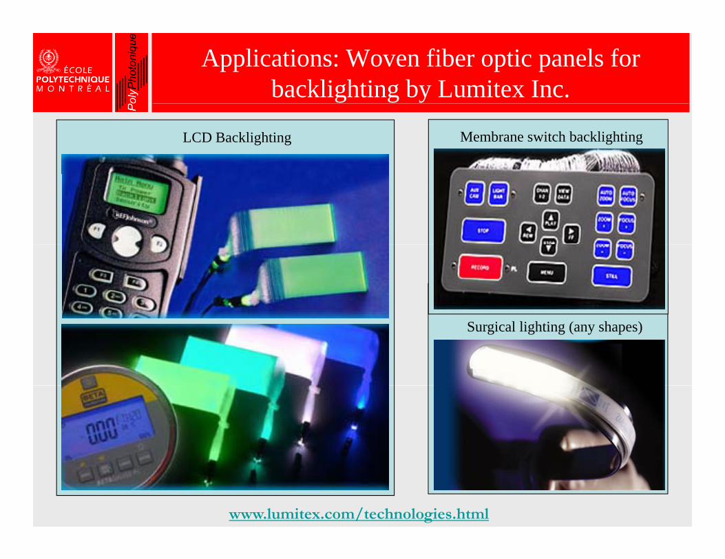
Applications: Woven fiber optic panels for backlighting by Lumitex Inc.
LCD Backlighting Membrane switch backlighting
Surgical lighting (any shapes)
www.lumitex.com/technologies.html
Applications: Fiber optic textiles for décor
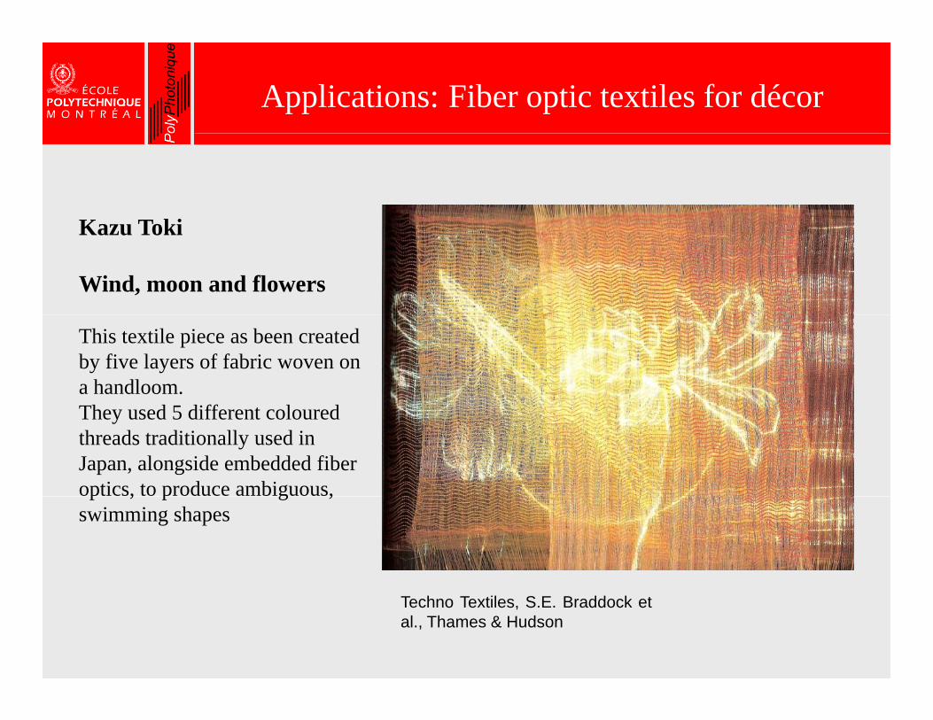
Ka TokiKazu Toki
Wind, moon and flowers
This textile piece as been created by five layers of fabric woven on a handloom. Th d 5 diff l dThey used 5 different coloured threads traditionally used in Japan, alongside embedded fiber optics, to produce ambiguous, p , p g ,swimming shapes
Techno Textiles, S.E. Braddock etal., Thames & Hudson
Applications: Fiber optic textiles for fashion
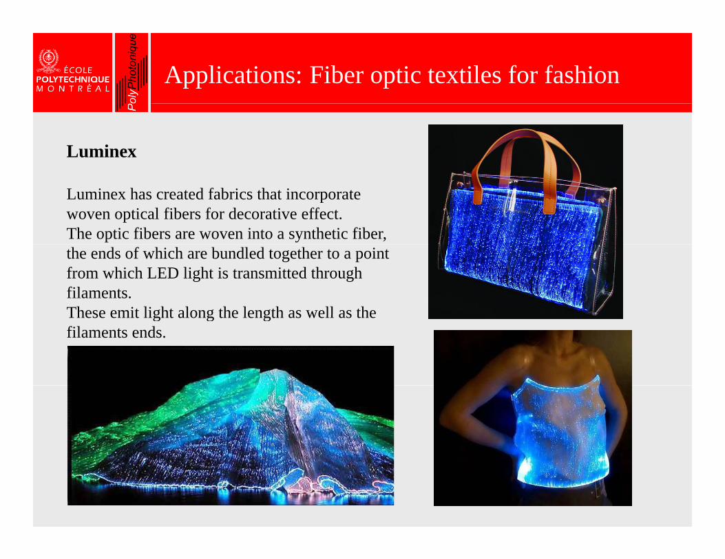
Luminex
Luminex has created fabrics that incorporate woven optical fibers for decorative effect.The optic fibers are woven into a synthetic fiber, the ends of which are bundled together to a point from which LED light is transmitted through filaments.These emit light along the length as well as theThese emit light along the length as well as the filaments ends.
Applications: Flexible screens made of woven optical fibres by France Telecom
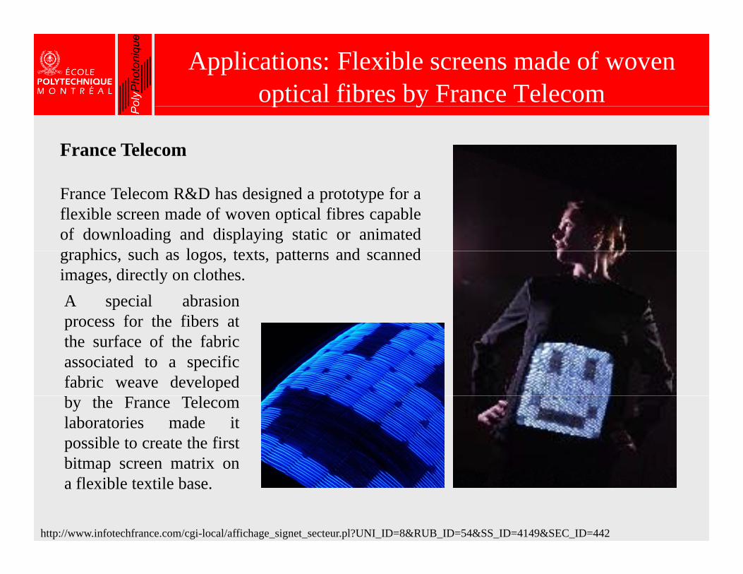
France Telecom
p y
France Telecom R&D has designed a prototype for aflexible screen made of woven optical fibres capableof downloading and displaying static or animated
hi h l t t tt d dgraphics, such as logos, texts, patterns and scannedimages, directly on clothes.A special abrasionprocess for the fibers atprocess for the fibers atthe surface of the fabricassociated to a specificfabric weave developedby the France Telecomlaboratories made itpossible to create the firstbitmap screen matrix on
http://www.infotechfrance.com/cgi-local/affichage_signet_secteur.pl?UNI_ID=8&RUB_ID=54&SS_ID=4149&SEC_ID=442
bitmap screen matrix ona flexible textile base.

Advantages of fiber drawing, non-optical applications of microstructured fibers
1. Fibers of very complex transverse geometries
Non-optical applicationstransverse geometries can be fabricated.
2. Several distinct materials (plastics, 1. Empty holes: heat isolating glasses, metals, semiconductors) can be integrated into the fiber crossection to integrate
textile2. Holes filled with phase
changing liquids - heat accumulating/releasingcrossection to integrate
complex functionalities.
3. Starting with i bj t
accumulating/releasing textile
3. Holes filled with anti-biotics + semi-permeable l ddi ti b t i l100ummacroscopic objects,
structures with sub-micron and even nano-sized features can be
cladding – anti-bacterial textile
4. Fiber made of piesoelectricmaterial + integrated metal
100um
fabricated.4. Highly cost effective.
gelectrodes – mechanically active textiles
Photonic Bandgap Fibers
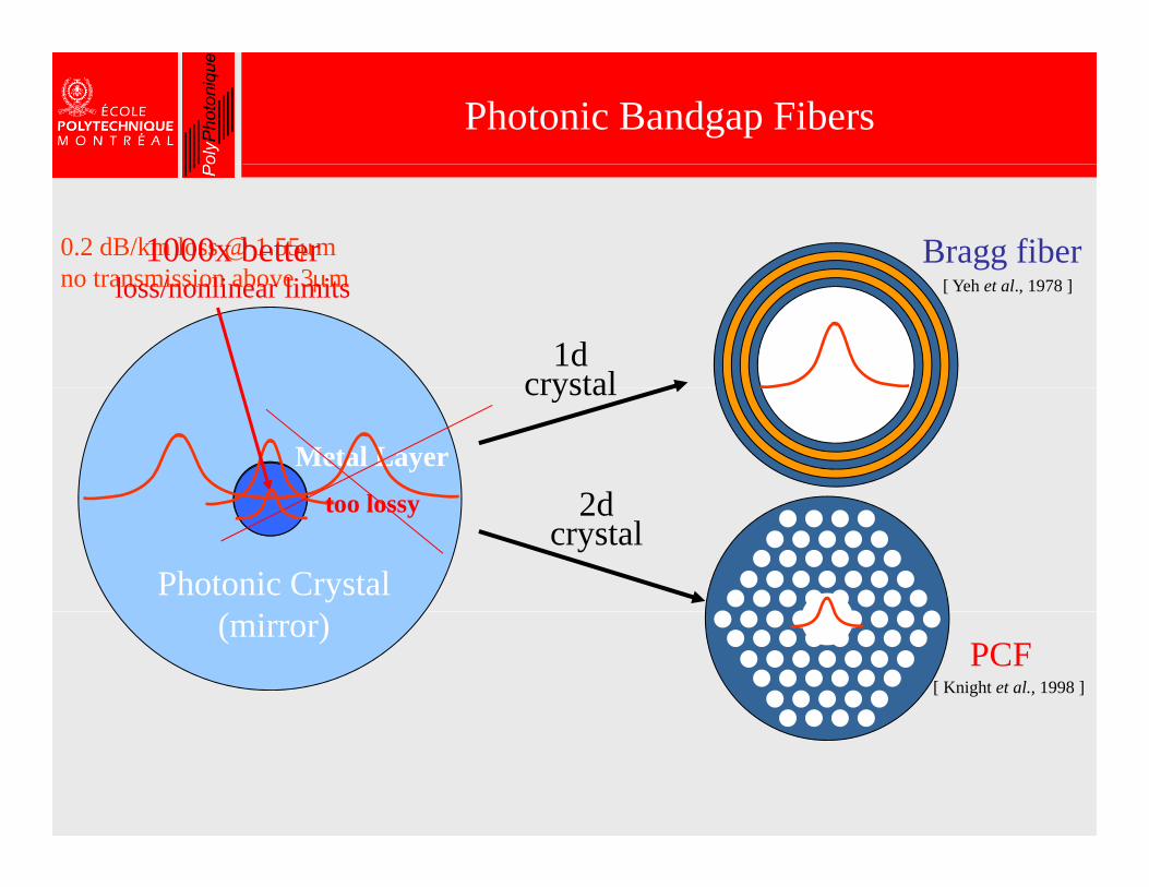
0.2 dB/km loss @ 1.55μmno transmission above 3μm
1000x better Bragg fiberno transmission above 3μmloss/nonlinear limits
1dcrystal
[ Yeh et al., 1978 ]
Metal Layert l
crystal
2dtoo lossy
Photonic Crystal
2dcrystal
(mirror)PCF
[ Knight et al., 1998 ]
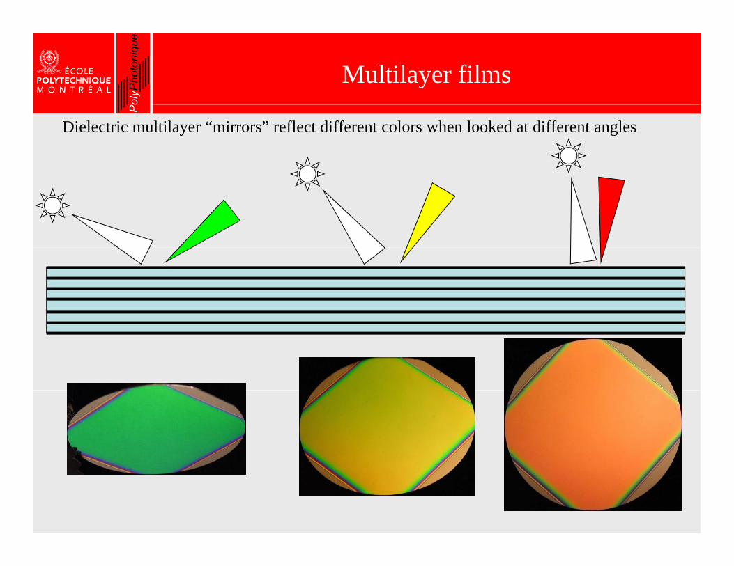
Multilayer films
Dielectric multilayer “mirrors” reflect different colors when looked at different angles
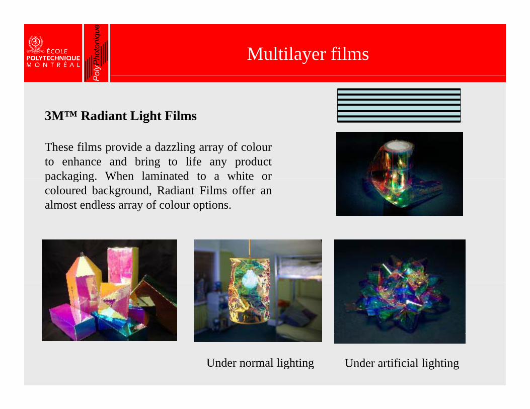
Multilayer films
3M™ Radiant Light Films
These films provide a dazzling array of colourto enhance and bring to life any productpackaging. When laminated to a white orpackaging. When laminated to a white orcoloured background, Radiant Films offer analmost endless array of colour options.
Under artificial lightingUnder normal lighting
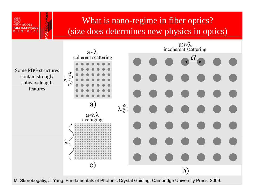
What is nano-regime in fiber optics?(size does determines new physics in optics)
Some PBG structures contain strongly subwavelength
features
M. Skorobogatiy, J. Yang, Fundamentals of Photonic Crystal Guiding, Cambridge University Press, 2009.

Three examples of guided nano-photonics
• Subwavelength structure in the fiber crossectionλ
Subwavelength structure in the fiber crossection (regular dielectrics, features < λ/5). PBG fibers (resonant light confinement)(resonant light confinement).
• Metallic inclusions that support plasmons (strongly confined modes with size < λ/5(strongly confined modes with size < λ/5-λ/20). Fibers and waveguides with integrated metallic elementsmetallic elements.
• Strongly subwavelength structure in the fiber ti ( l di l t i f t λ/20)crossection (regular dielectrics, features < λ/20).
Porous subwavelength fibers (metamaterial).λ/10
I
• Photonic bandgap fibers feature highlyPhotonic bandgap fibers feature highly subwavelength features in their crossection, while still operating in the regime of coherentwhile still operating in the regime of coherent scattering (resonant confinement).

Most PBG structures contain strongly subwavelength inclusions
Hollow core PBG fibers have highly subwavelength features(applications in high-power laser light transmission, liquid-filled core sensing in biotech,(applications in high power laser light transmission, liquid filled core sensing in biotech, gas-filled core sensing, photonic textiles, ultra-low nonlinearity telecom applications, etc.)
Bragg fibersL hi k h λ/4/
Hollow core Photonic Bandgap Fibersi l i hi k h ld b llLayer thickness h ~ λ/4/n
Polymers (n=1.5) h < λ/5Chalcogenide glass (n=2.8) h < λ/10
material vein thickness should be smaller than 2-5% of the period Λ~ λ, thus hvein < λ/20

All-Polymer Bragg fiber preforms via Co-Rolling of polymer films
Polymer or glassPolymer or glassPolymer film 1
Polymer or glass mandrel (cylinder)Polymer or glass
mandrel (cylinder)can be removed
after rollingPolymer film 2
E. Pone, M. Skorobogatiy et al., "Drawing of the hollow all-polymer Bragg fibers," Optics Express 14, 5838 (2006)

‘ColorFull’ plastic fibers for advanced textiles, short-range communications and sensing
A. Dupuis, N. Guo, B. Gauvreau, A. Hassani, E. Pone, F. Boismenu, and M. Skorobogatiy, "Guiding in the visible with "colorful" solid-core Bragg fibers," Opt. Lett. 32, 2882-2884 (2007).

Transmitted and emitted colors
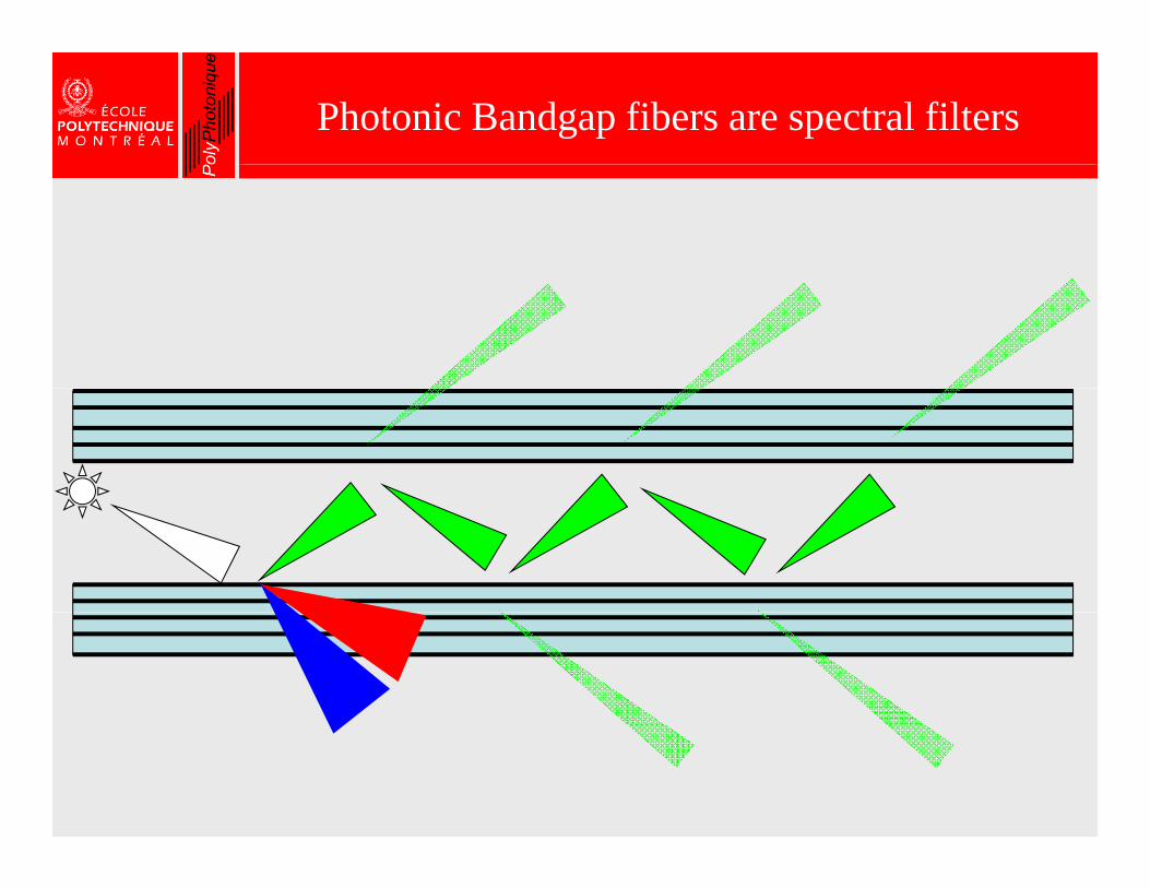
Photonic Bandgap fibers are spectral filters

Bangap shift due to fiber elongationapplications in sensing of strain
B. Gauvreau, N. Guo, K. Schicker, K. Stoeffler, F. Boismenu, A. Ajji, R. Wingfield, C. Dubois, M. Skorobogatiy, "Color-changing and color-tunable photonic bandgap fiber textiles," Opt. Express, Vol. 16, pp. 15677-15693 (2008).
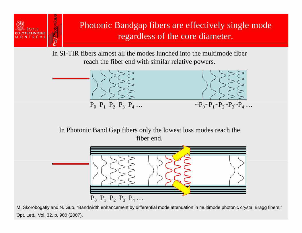
Photonic Bandgap fibers are effectively single mode regardless of the core diameter.
In SI-TIR fibers almost all the modes lunched into the multimode fiber reach the fiber end with similar relative powers.
P0 P1 P2 P3 P4 … ~P0~P1~P2~P3~P4 …
In Photonic Band Gap fibers only the lowest loss modes reach theIn Photonic Band Gap fibers only the lowest loss modes reach the fiber end.
P0 P1 P2 P3 P4 …M. Skorobogatiy and N. Guo, “Bandwidth enhancement by differential mode attenuation in multimode photonic crystal Bragg fibers,”
Opt. Lett., Vol. 32, p. 900 (2007).

PBG fiber bundles, application in colorful illumination and all-fiber spectral filtering
WHITE LIGHT INPUT
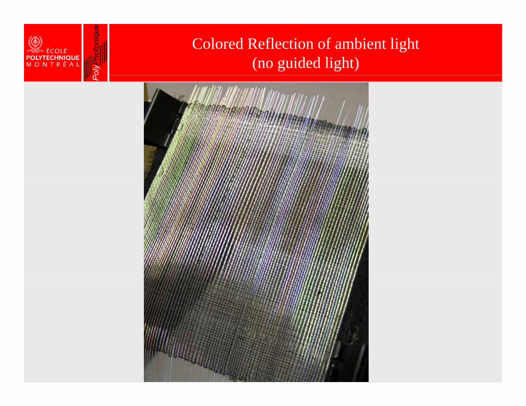
Colored Reflection of ambient light (no guided light)

Photonic textiles using photonic bandgap fibersB. Gauvreau, M. Skorobogatiy et al. "Color-changing and color-tunable photonic bandgap fiber textiles," Opt. Express,
Vol. 16, pp. 15677-15693 (2008).
Nature Photonics – News and Views, Color-tunable textiles, Nov. 2008

Changing textile appearance by mixing the ambient and emitted light
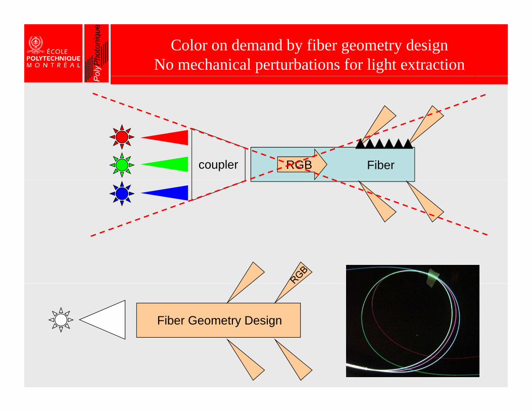
Color on demand by fiber geometry designNo mechanical perturbations for light extraction
Fibercoupler RGB
Fiber Geometry Design
Photonic Bandgap Textiles
VIDEOVIDEO
II
• Fibers and waveguides with integratedFibers and waveguides with integrated metallic elements can support highly localized plasmonic modes with size < λ/5-λ/20plasmonic modes with size < λ/5-λ/20.
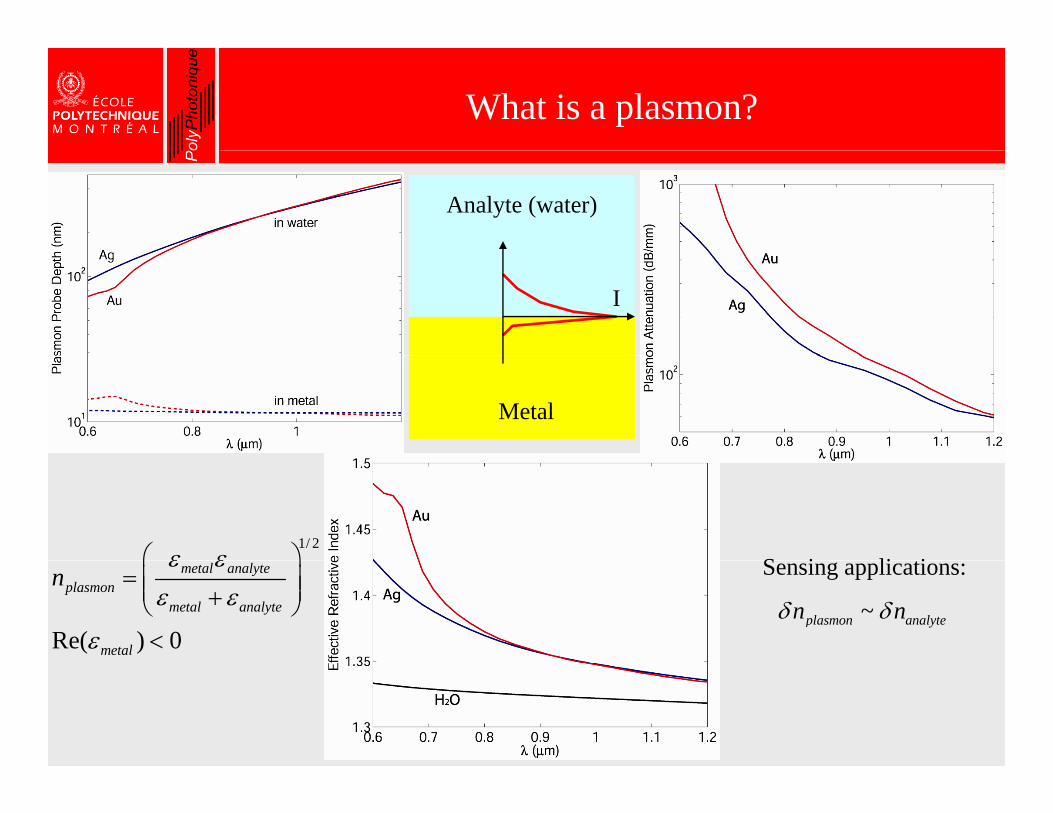
What is a plasmon?
Analyte (water)
I
Metal
1/ 2ε ε⎛ ⎞ S i li ti
~plasmon analyten nδ δRe( ) 0
metal analyteplasmon
metal analyte
metal
nε ε
ε ε
ε
⎛ ⎞= ⎜ ⎟⎜ ⎟+⎝ ⎠
<
Sensing applications:
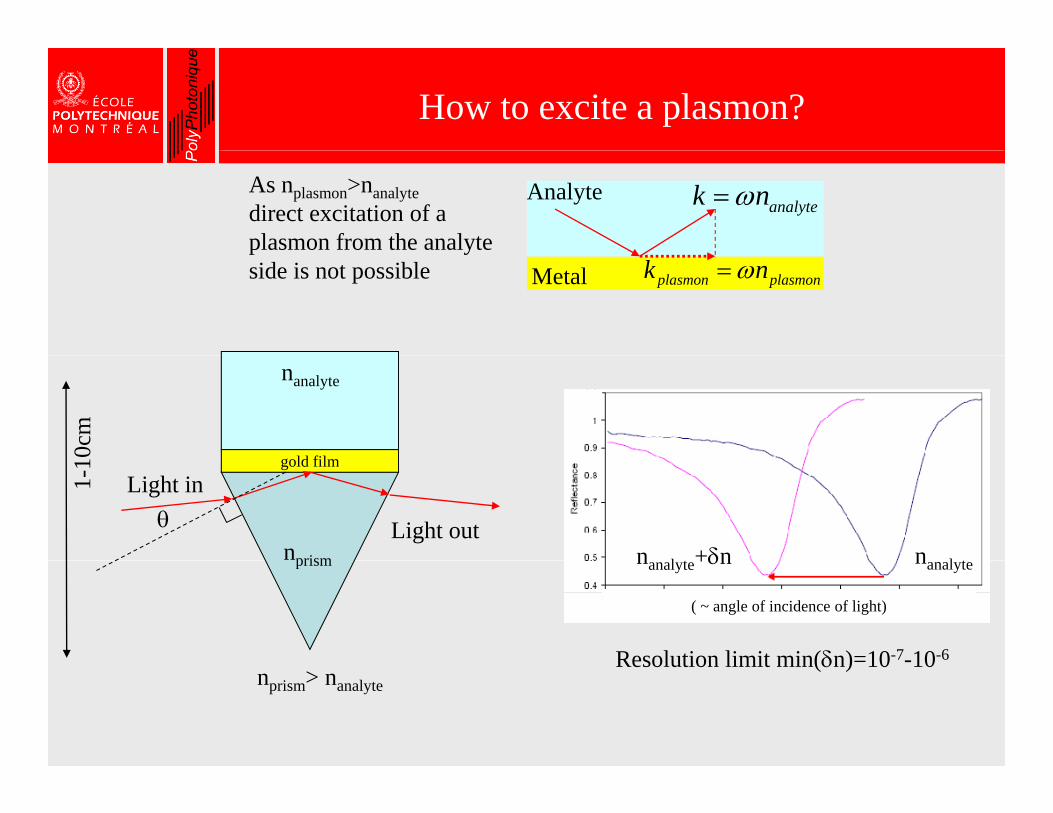
How to excite a plasmon?
analytek nω=AnalyteAs nplasmon>nanalytedirect excitation of a plasmon from the analyte
Metalp yside is not possible plasmon plasmonk nω=
analytek nω=
ld fil
nanalyte
0cm
n l tn l t +δn
Light ingold film
Light outθnprism
1-1
( ~ angle of incidence of light)
nanalytenanalyte+δn
Resolution limit min(δn)=10-7-10-6
prism
Resolution limit min(δn) 10 10nprism> nanalyte
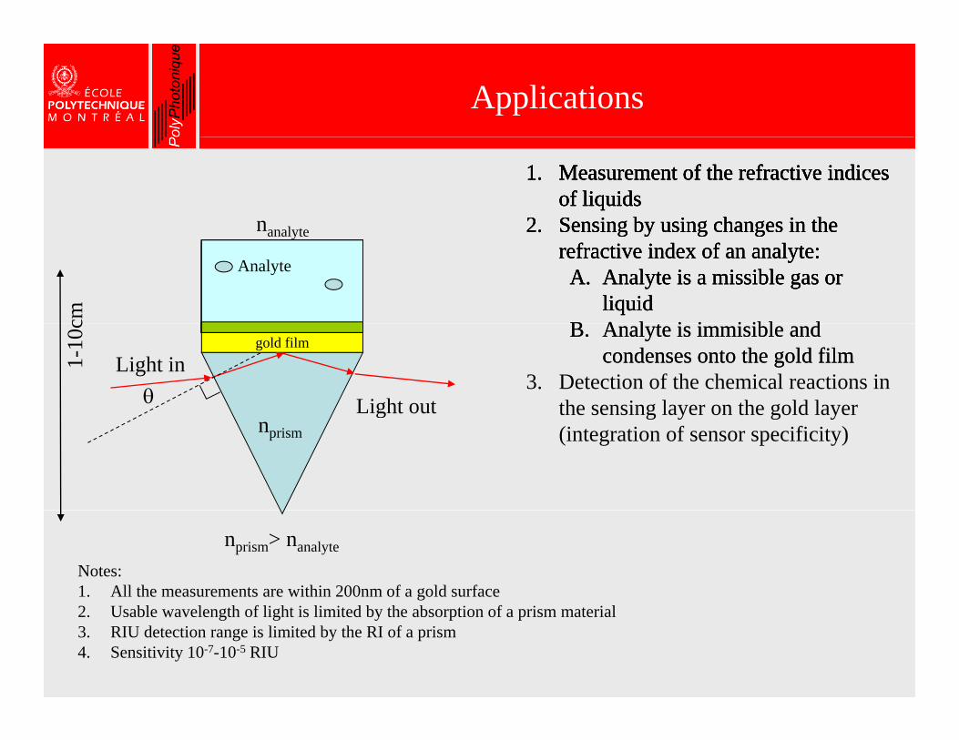
Applications
nanalyte
1. Measurement of the refractive indices of liquids
2. Sensing by using changes in the
1. Measurement of the refractive indices of liquids
2. Sensing by using changes in the
1. Measurement of the refractive indices of liquids
1. Measurement of the refractive indices of liquids
2. Sensing by using changes in thenanalyte
cm
2. Sensing by using changes in the refractive index of an analyte:A. Analyte is a missible gas or
liquid
2. Sensing by using changes in the refractive index of an analyte:A. Analyte is a missible gas or
liquidB A l t i i i ibl d
2. Sensing by using changes in the refractive index of an analyte:A. Analyte is a missible gas or
liquidB A l t i i i ibl d
Analyte
Chemical reaction
Analyte
gold film
1-10
c B. Analyte is immisible and condenses onto the gold film
B. Analyte is immisible and condenses onto the gold film
3. Detection of the chemical reactions in the sensing layer on the gold layer
Light in
Light outθnprism
g y g y(integration of sensor specificity)
g
nprism> nanalyte
Notes: 1. All the measurements are within 200nm of a gold surface2. Usable wavelength of light is limited by the absorption of a prism material3. RIU detection range is limited by the RI of a prism4. Sensitivity 10-7-10-5 RIU
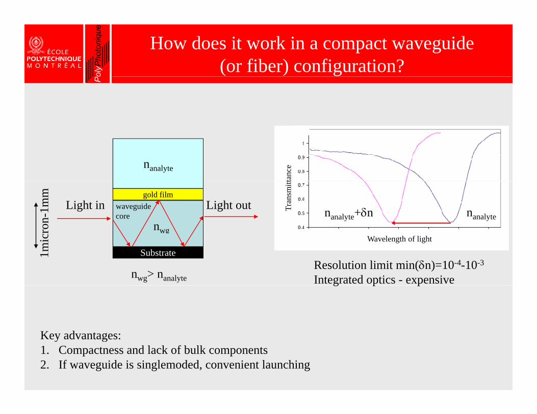
How does it work in a compact waveguide (or fiber) configuration?
nanalyte
tanc
e
Light ingold film
Light out
nwg
nanalytenanalyte+δn
ron-
1mm
waveguide core
Tran
smitt
nwg> nanalyte
Wavelength of light
Resolution limit min(δn)=10-4-10-3
Integrated optics - expensive
Substrate1mic
r
g p p
Key advantages:Key advantages:1. Compactness and lack of bulk components2. If waveguide is singlemoded, convenient launching

Applications in bio-sensing
1. Metal layer is first bio-functionalized with a nanometer thick analyte ‘recognition’ bio-molecules
nanalyte
bio molecules.
2. When analyte molecules are present in a suspension, some of them are captured by the ‘recognition’ molecules and held on a
Light ingold film
Light out
nwg
waveguide core
the recognition molecules and held on a gold surface. By detecting refractive index change in the nanometer thick bio-layer due to binding of bio-molecules (n~1.42) one
d t t f h l l
nwg> nanalyte
Substrate
can detect presence of such molecules.
3. Sensitivity can be further enhanced if metal nanoparticles are bound to the
l t l l I thi d d t t
Notes:
analyte molecules. In this mode one detects effective changes in thickness of a sensing metal layer.
1. All the measurements are within 200nm of a gold surface2. Usable wavelength of light is limited by the absorption of a waveguide core material3. RIU detection range is limited by the waveguide core and cladding indexes4. Sensitivity 10-7-10-5 RIU
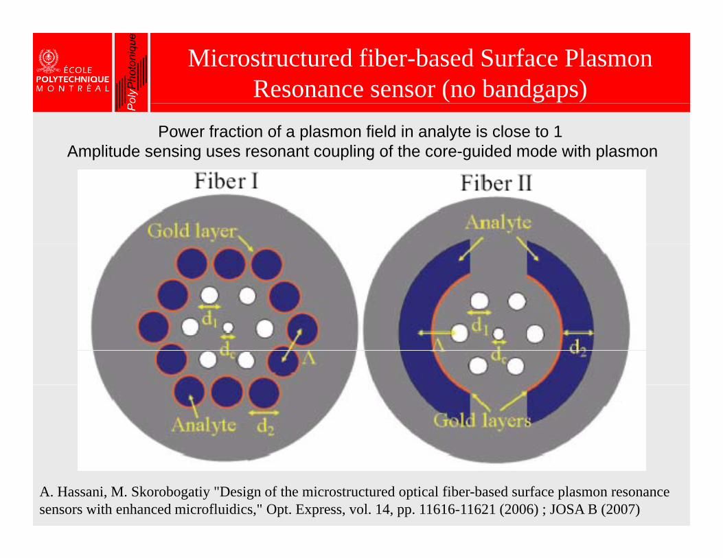
Microstructured fiber-based Surface Plasmon Resonance sensor (no bandgaps)
Power fraction of a plasmon field in analyte is close to 1 Amplitude sensing uses resonant coupling of the core-guided mode with plasmon
A. Hassani, M. Skorobogatiy "Design of the microstructured optical fiber-based surface plasmon resonance sensors with enhanced microfluidics," Opt. Express, vol. 14, pp. 11616-11621 (2006) ; JOSA B (2007)

Dispersion relations of a core-guided mode and a surface plasmon in the vicinity of phase-matching point.
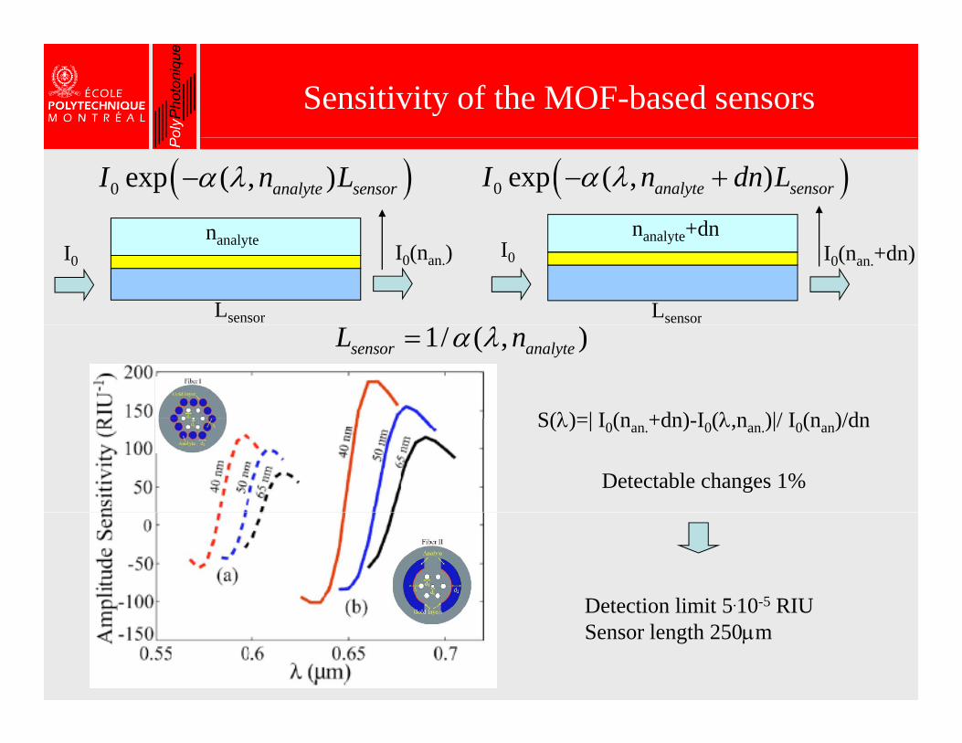
Sensitivity of the MOF-based sensors
( )0 exp ( , )analyte sensorI n Lα λ−
n n l +dn
( )0 exp ( , )analyte sensorI n dn Lα λ− +
Lsensor
nanalyteI0 I0(nan.)
Lsensor
nanalyte+dnI0 I0(nan.+dn)
1/ ( , )sensor analyteL nα λ=
S(λ)=| I (n +dn) I (λ n )|/ I (n )/dn
Detectable changes 1%
S(λ)=| I0(nan.+dn)-I0(λ,nan.)|/ I0(nan)/dn
Detection limit 5.10-5 RIUDetection limit 5.10 5 RIUSensor length 250μm

YES, IT IS POSSIBLE to Metalized the Holes inside Microstructured Fibers
A micrograph of the structure, indicating the two coated holes (top). Elemental analysis shows the presence of silver (dots in the image) An SEM of the silver surface of a coated hole is shownthe presence of silver (dots in the image). An SEM of the silver surface of a coated hole is shown on the right.
X. Zhang, R. Wang, F. M. Cox, B.T. Kuhlmey, and M. C. J. Large, “Selective coating of holes in microstructured optical fiber and its application g g y g g p ppto in-fiber absorptive polarizers,” opt. express, 16270-16278, 2007

Single Mode vs. Multimode vs. Photonic Crystal waveguides
1. Sensitiv. 10-5-10-3 RIU2. Almost any choice of
wg materials is fine.3 I i t d
1. Sensitiv. 10-4-10-3 RIU2. Hard to choose proper wg
materials, especially for air and t b d i
1. Sensitiv. 10-5-10-3 RIU2. Almost any choice of
wg materials is fine3 C i t d t bl3. Inconvenient and
unstable couplingwater based sensing
3. Convenient and stable coupling3. Convenient and stable
coupling
Nature Photonics - Plasmonics: Sensors tune in, Oct. 2006 M. Skorobogatiy, Kabashin, “Photon Crystal waveguide-based surface plasmon resonance bio-sensor,” Appl. Phys. Lett. 89, 143518 (2006) M. Skorobogatiy, Kabashin, “Plasmon excitation by the Gaussian-like core mode of a photonic crystal waveguide,” Opt. Express 14, 8419 (2006)

Dispersion relations of the core guided and plasmon modes, planar waveguides
B. Gauvreau, A. Hassani, M. Fassi Fehri, A. Kabashin, and M. A. Skorobogatiy, "Photonic bandgap fiber-based Surface Plasmon Resonance sensors," Opt Express, vol 15, 11413-11426 (2007)sensors, Opt. Express, vol. 15, 11413 11426 (2007).
Nature Photonics - Plasmonics: Sensors tune in, Oct. 2006

Energy flux in a multilayer waveguide for various values of the ambient refractive index
Amplitude Based Sensing
Sensitivity: change in the bulk refractive index resulting in 1% change of the signal amplitude
Optimal designs have theoretical sensitivity as low as 7.10-6 RIU
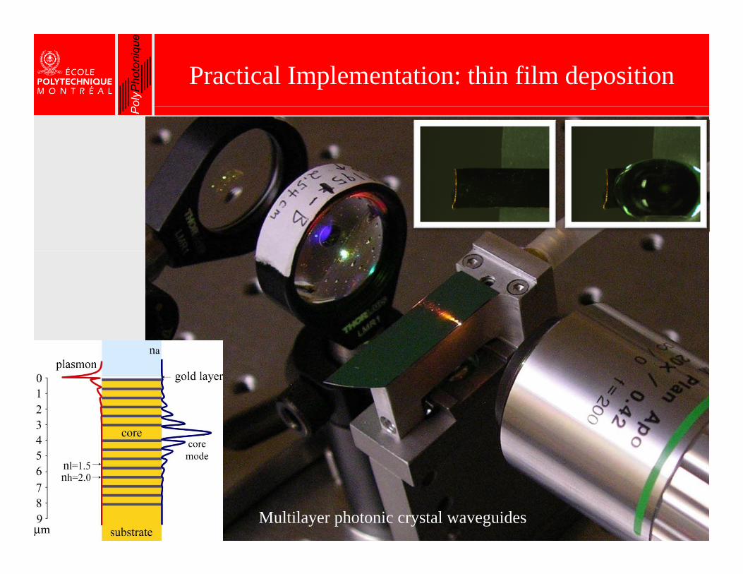
Practical Implementation: thin film deposition
Multilayer photonic crystal waveguides
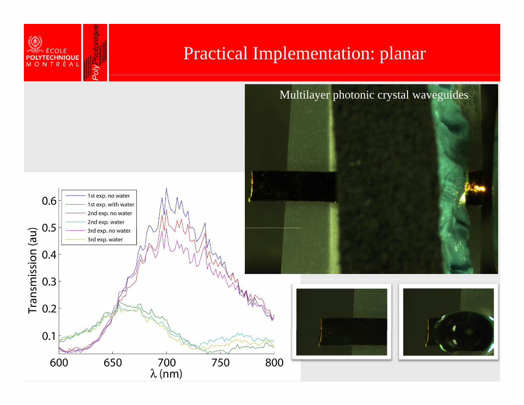
Practical Implementation: planar
Multilayer photonic crystal waveguides
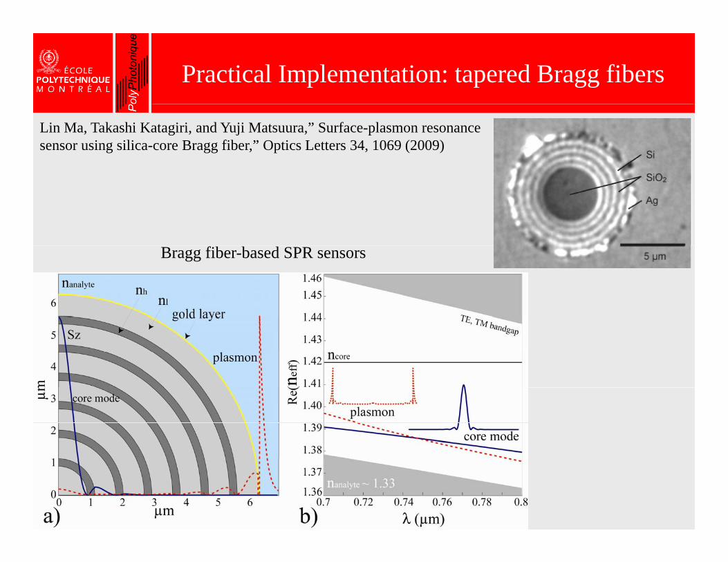
Practical Implementation: tapered Bragg fibers
Lin Ma, Takashi Katagiri, and Yuji Matsuura,” Surface-plasmon resonance sensor using silica-core Bragg fiber,” Optics Letters 34, 1069 (2009)
Bragg fiber-based SPR sensors
III
• Fibers with outer diameters comparable to theFibers with outer diameters comparable to the wavelength of light, while having highly subwavelength features in their crossectionsubwavelength features in their crossection typically operate in the metamaterial regime
Applications of THz
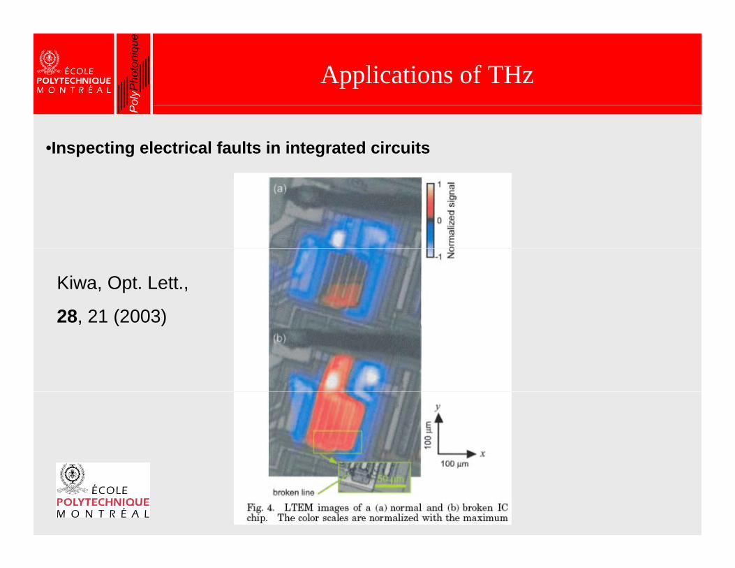
•Inspecting electrical faults in integrated circuits
Kiwa, Opt. Lett.,
28 21 (2003)28, 21 (2003)

Applications of THz
• Tomography Pearce, Opt. Lett., 30, 13 (2005)
Mittleman, Opt. Lett., 22, 12 (1997)

Applications of THz
•Chemical recognition of gases and biomolecules
Time domain spectroscopy
Jacobsen, Opt. Lett., 21, 24 (1996)
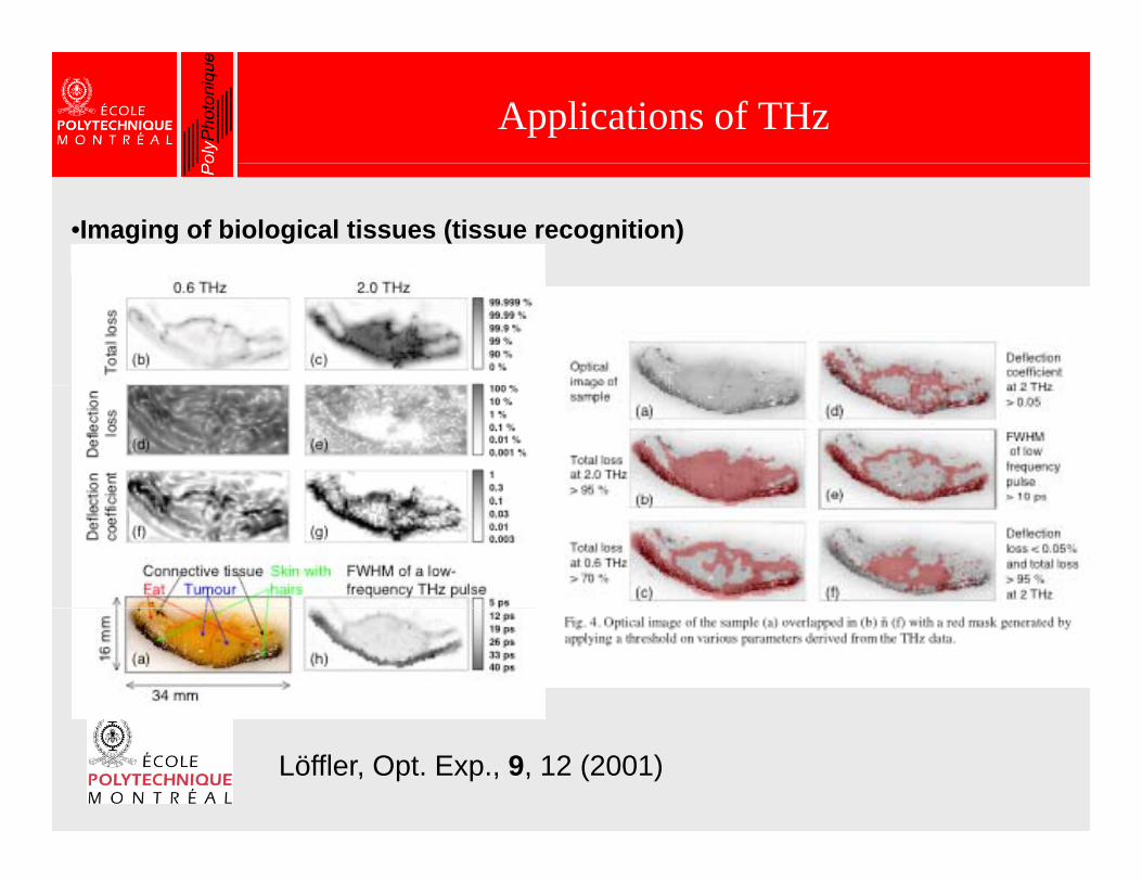
Applications of THz
•Imaging of biological tissues (tissue recognition)
Löffler, Opt. Exp., 9, 12 (2001)
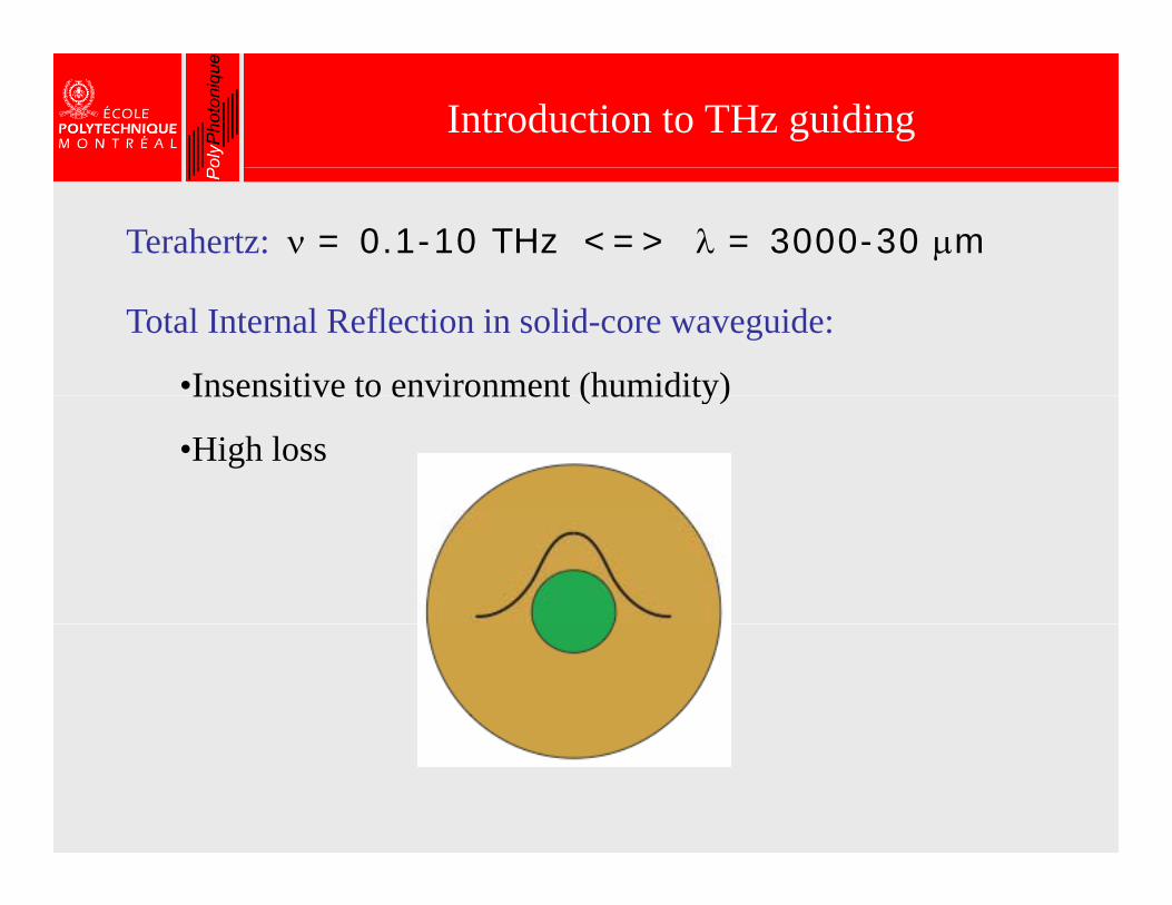
Introduction to THz guiding
Terahertz: ν = 0.1-10 THz <=> λ = 3000-30 μm
Total Internal Reflection in solid-core waveguide:
•Insensitive to environment (humidity)Insensitive to environment (humidity)
•High loss
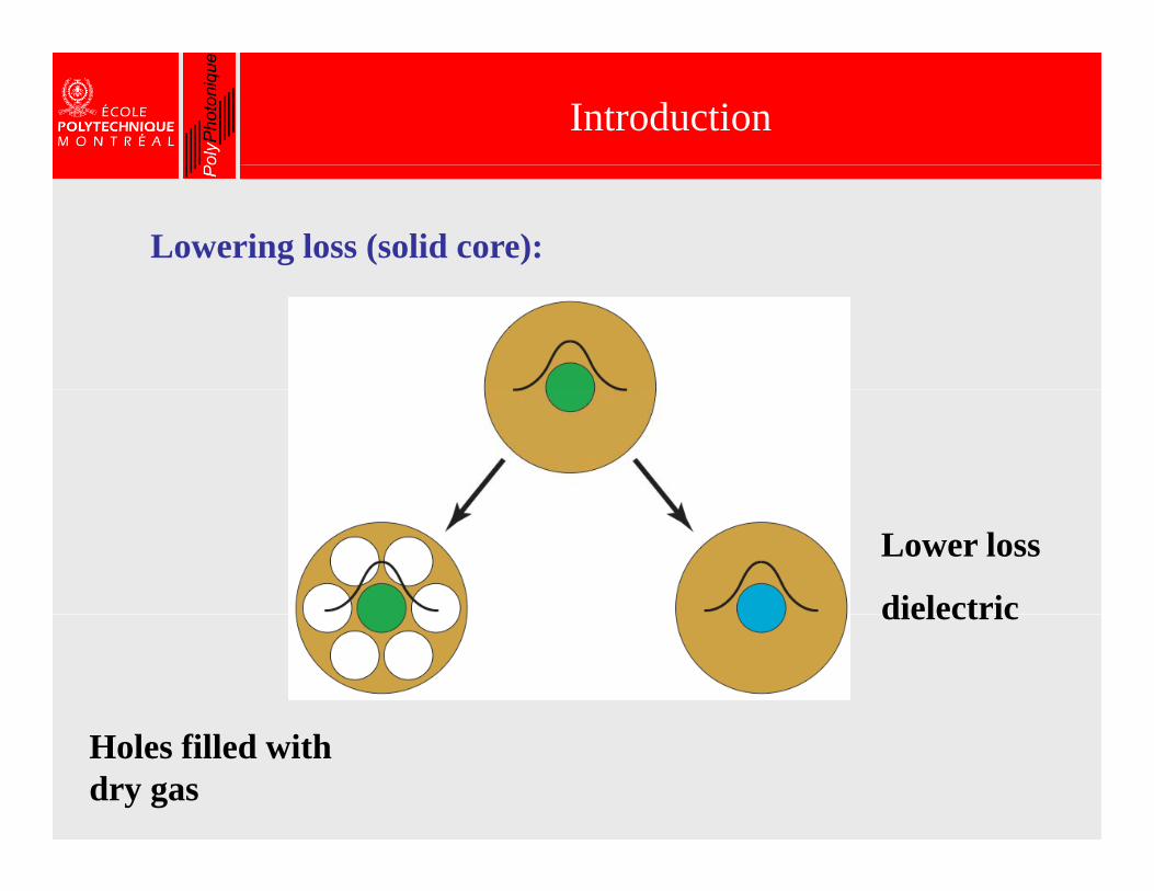
Introduction
Lowering loss (solid core):
Lower loss
dielectricdielectric
Holes filled withdry gas

Introduction
Lowering loss (hollow core):
Capillary
Metallic PorousTIR
PCF
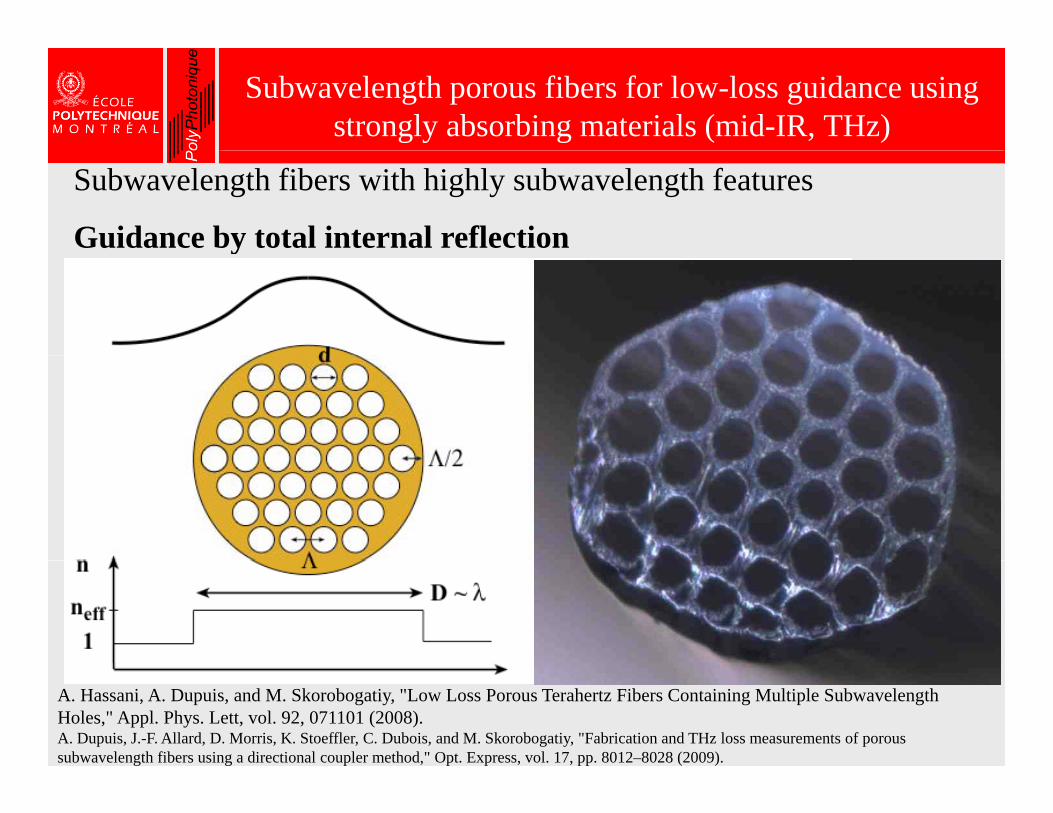
Subwavelength porous fibers for low-loss guidance using strongly absorbing materials (mid-IR, THz)
Subwavelength fibers with highly subwavelength features
Guidance by total internal reflectiony
A. Hassani, A. Dupuis, and M. Skorobogatiy, "Low Loss Porous Terahertz Fibers Containing Multiple SubwavelengthHoles," Appl. Phys. Lett, vol. 92, 071101 (2008). A. Dupuis, J.-F. Allard, D. Morris, K. Stoeffler, C. Dubois, and M. Skorobogatiy, "Fabrication and THz loss measurements of porous subwavelength fibers using a directional coupler method," Opt. Express, vol. 17, pp. 8012–8028 (2009).

Subwavelength porous fibers
at 1THz, λ=300μmnfiber=1.5αm=1cm-1=435dB/m
To reduce material loss by a factor of 10:D λ (300 m)D ~ λ (300μm)d ~ 0.1λ (30μm)hvein=Λ-d ~ 0.01λ (3μm)

Subwavelength porous fibers
at 1THz, λ=300μmnfiber=1.5; αm=1cm-1=435dB/m
Conclusions
• We have discussed three examples of optical fibers whose operationWe have discussed three examples of optical fibers whose operation relies on presence of nano-sized structure in the fiber crossection.
• First example was photonic bandgap Bragg fibers containing highly subwavelength layers (λ/10) to provide resonant light confinement in g y ( ) p gthe low refractive index core. Application in sensing, and photonic textiles.
• Second example was photonic crystal fibers containing metallic p p y ginclusions. In this configuration, highly localized and lossy plasmonic modes (λ/5) could be coupled to guided core modes. Application in compact and highly sensitive sensors of refractive i dindex.
• Third example was a porous subwavelength fiber that guides light predominantly in the subwavelength air gaps (λ/10) surrounded by even thinner (λ/100) material veins (metamaterial) Application ineven thinner (λ/100) material veins (metamaterial). Application in low-loss guidance with even highly lossy materials (mid IR, THz).

Acknowledgements
• Prof. C. Dubois• Prof. J. Berzowska (Concordia U.)• Designer Kathy Shicker (University of the
Arts London)Arts London) • Res. Assoc. E. Pone• PhD N. Guo• PhD A. Dupuis• PhD A. Hassani• MSc B. Gauvreau
• The Natural Sciences and Engineering Research Council of Canada
• Fonds Québécois de la Recherche sur la Nature et les Technologies
• Canada Research Chair Foundation
• Canadian Institute for Photonics Innovations