boot-mips: example boot code for mips® cores · violation of the law of any country or...
TRANSCRIPT

Boot-MIPS: Example Boot Code for MIPS® Cores
This application note describes Boot-MIPS, an example boot code for MIPS processor cores. Boot-MIPS is a stand-alone
executable that runs from reset, initializing core resources to the point where every processing element in the system is executing shared C code, with its own stack and coherent shared global data.
Document Number: MD00901 Revision 1.02
August 19, 2013
Imagination Technologies Limited 955 East Arques Avenue
Sunnyvale, CA 94085-4521
Copyright © 2013 Imagination Technologies Limited All rights reserved.

Boot-MIPS: Example Boot Code, Revision 01.03 Copyright © 2013 Imagination Technologies Limited. All rights reserved.
Page 2
Unpublished rights (if any) reserved under the copyright laws of the United States of America and other countries. This document contains information that is proprietary to MIPS Technologies, Inc. ("MIPS Technologies") one of the Imagination Technologies Group plc companies Any copying, reproducing, modifying or use of this information (in whole or in part) that is not expressly permitted in writing by MIPS Technologies or an authorized third party is strictly prohibited. At a minimum, this information is protected under unfair competition and copyright laws. Violations thereof may result in criminal penalties and fines. This document contains information that is proprietary to MIPS Technologies, Inc. ("MIPS Technologies"). Any copying, reproducing, modifying or use of this information (in whole or in part) that is not expressly permitted in writing by MIPS Technologies or an authorized third party is strictly prohibited. At a minimum, this information is protected under unfair competition and copyright laws. Violations thereof may result in criminal penalties and fines. Any document provided in source format (i.e., in a modifiable form such as in FrameMaker or Microsoft Word format) is subject to use and distribution restrictions that are independent of and supplemental to any and all confidentiality restrictions. UNDER NO CIRCUMSTANCES MAY A DOCUMENT PROVIDED IN SOURCE FORMAT BE DISTRIBUTED TO A THIRD PARTY IN SOURCE FORMAT WITHOUT THE EXPRESS WRITTEN PERMISSION OF MIPS TECHNOLOGIES, INC. MIPS Technologies reserves the right to change the information contained in this document to improve function, design or otherwise. MIPS Technologies does not assume any liability arising out of the application or use of this information, or of any error or omission in such information. Any warranties, whether express, statutory, implied or otherwise, including but not limited to the implied warranties of merchantability or fitness for a particular purpose, are excluded. Except as expressly provided in any written license agreement from MIPS Technologies or an authorized third party, the furnishing of this document does not give recipient any license to any intellectual property rights, including any patent rights, that cover the information in this document. The information contained in this document shall not be exported, reexported, transferred, or released, directly or indirectly, in violation of the law of any country or international law, regulation, treaty, Executive Order, statute, amendments or supplements thereto. Should a conflict arise regarding the export, reexport, transfer, or release of the information contained in this document, the laws of the United States of America shall be the governing law. The information contained in this document constitutes one or more of the following: commercial computer software, commercial computer software documentation or other commercial items. If the user of this information, or any related documentation of any kind, including related technical data or manuals, is an agency, department, or other entity of the United States government ("Government"), the use, duplication, reproduction, release, modification, disclosure, or transfer of this information, or any related documentation of any kind, is restricted in accordance with Federal Acquisition Regulation 12.212 for civilian agencies and Defense Federal Acquisition Regulation Supplement 227.7202 for military agencies. The use of this information by the Government is further restricted in accordance with the terms of the license agreement(s) and/or applicable contract terms and conditions covering this information from MIPS Technologies or an authorized third party. MIPS, MIPS I, MIPS II, MIPS III, MIPS IV, MIPS V, MIPSr3, MIPS32, MIPS64, microMIPS32, microMIPS64, MIPS-3D, MIPS16, MIPS16e, MIPS-Based, MIPSsim, MIPSpro, MIPS Technologies logo, MIPS-VERIFIED, MIPS-VERIFIED logo, 4K, 4Kc, 4Km, 4Kp, 4KE, 4KEc, 4KEm, 4KEp, 4KS, 4KSc, 4KSd, M4K, M14K, 5K, 5Kc, 5Kf, 24K, 24Kc, 24Kf, 24KE, 24KEc, 24KEf, 34K, 34Kc, 34Kf, 74K, 74Kc, 74Kf, 1004K, 1004Kc, 1004Kf, 1074K, 1074Kc, 1074Kf, R3000, R4000, R5000, Aptiv, ASMACRO, Atlas, "At the core of the user experience.", BusBridge, Bus Navigator, CLAM, CorExtend, CoreFPGA, CoreLV, EC, FPGA View, FS2, FS2 FIRST SILICON SOLUTIONS logo, FS2 NAVIGATOR, HyperDebug, HyperJTAG, IASim, interAptiv, JALGO, Logic Navigator, Malta, MDMX, MED, MGB, microAptiv, microMIPS, OCI, PDtrace, the Pipeline, proAptiv, Pro Series, SEAD, SEAD-2, SmartMIPS, SOC-it, System Navigator, and YAMON are trademarks or registered trademarks of MIPS Technologies, Inc. in the United States and other countries. All other trademarks referred to herein are the property of their respective owners. All other trademarks referred to herein are the property of their respective owners.

Boot-MIPS: Example Boot Code, Revision 01.03 Copyright © 2013 Imagination Technologies Limited. All rights reserved.
Page 3
Table of Contents 1 Introduction .................................................................................................................................. 7
1.1 Terminology .................................................................................................................................. 7
1.2 Tools.............................................................................................................................................. 8
2 Installation .................................................................................................................................... 9
2.1.1 Installing as a NavigatorICS Project....................................................................................... 9
3 Boot‐MIPS Package .....................................................................................................................14
3.1.1 Directories...........................................................................................................................14
3.1.2 Core Directory Files.............................................................................................................14
3.1.3 Common Directory Files......................................................................................................15
3.1.4 cps Directory Files ...............................................................................................................15
3.1.5 Malta Directory files............................................................................................................15
3.1.6 mt Directory Files ................................................................................................................15
3.1.7 Other files in the top directory ...........................................................................................16
4 Building the Project.....................................................................................................................16
4.1 Target Selection ..........................................................................................................................16
4.2 Build the selected Target ............................................................................................................18
5 Code Details ................................................................................................................................19
5.1 common/boot.h..........................................................................................................................22
5.2 start.S ..........................................................................................................................................24
5.2.1 Boot Exception Vector ........................................................................................................25
5.2.2 Other Exceptions.................................................................................................................25
5.2.3 Multi ‐core inter‐processor interrupt processing (1004K, 1074K, interAptiv and proAptiv CPS only). ............................................................................................................................................26
5.2.4 Ejtag Exception....................................................................................................................27
5.2.5 NMI, ISA, and MIPS32 Verification......................................................................................27
5.2.6 Initializing Common Resources ...........................................................................................28
5.2.7 Initialize System Resources .................................................................................................30
5.2.8 Initializing Core Resources ..................................................................................................32
5.2.9 Initialization Complete ........................................................................................................33
5.3 set_gpr_boot_values.S................................................................................................................34

Boot-MIPS: Example Boot Code, Revision 01.03 Copyright © 2013 Imagination Technologies Limited. All rights reserved.
Page 4
5.3.1 MT ASE Check (34K and 1004K CPS Only)...........................................................................36
5.3.2 No MT ASE (24K, 74K, 1074K, and proAptiv) ....................................................................37
5.3.3 Check for Coherent Processing System (1004K, 1074K, interAptiv or proAptiv)................37
5.3.4 Not a Coherent Processing System (24K, 34K, and 74K).....................................................37
5.3.5 Is a Coherent Processing System (1004K, 1074K, interAptiv or proAptiv only)..................37
5.3.6 Done with set_gpr_boot_values.........................................................................................39
5.4 common/copy_2c_ram.S ............................................................................................................40
5.5 common/copy_2c_SPram.S ........................................................................................................43
5.5.1 Copy to Instruction Scratch Pad..........................................................................................43
5.5.2 Copy to Data Scratch Pad....................................................................................................47
5.6 common/copy_c2_Spram_MM.S (microAptiv cores).................................................................50
5.7 common/init_caches.S (non‐proAptiv cores) .............................................................................57
5.7.1 init_icache ...........................................................................................................................57
5.7.2 init_dcache..........................................................................................................................60
5.7.3 change_k0_cca....................................................................................................................60
5.7.4 init_l23u ..............................................................................................................................61
5.8 init_L23caches.S..........................................................................................................................63
5.8.1 Init_l23c............................................................................................................................... 63
5.8.2 init_l23 ................................................................................................................................64
5.9 common/init_caches2.s (proAptiv and interAptiv Cores only)...................................................66
5.9.1 init_icache ...........................................................................................................................66
5.9.2 init_dcache..........................................................................................................................68
5.9.3 disable_l23 ..........................................................................................................................70
5.9.4 init_L23................................................................................................................................71
5.10 common/init_cp0........................................................................................................................71
5.10.1 Initialize the CP0 Status register .........................................................................................71
5.10.2 Initialize the Watch Registers..............................................................................................72
5.10.3 Clear the Compare Register ................................................................................................73
5.11 common/init_gpr.S .....................................................................................................................73
5.12 common/init_tlb (non proAptiv cores only) ...............................................................................74
5.13 common/init_tlb2 (proAptiv cores only) ....................................................................................77
5.14 cps/init_cm.S Coherence manager (CPS systems, 1004K and 1074K only) ................................79
5.15 cps/init_cpc.S Cluster Power Controller (CPS systems, 1004K, 1074K, proAptiv and interAptiv only) 81

Boot-MIPS: Example Boot Code, Revision 01.03 Copyright © 2013 Imagination Technologies Limited. All rights reserved.
Page 5
5.16 cps/init_gic.S Global Interrupt Controller (CPS systems, 1004K and 1074K only)......................82
5.16.1 Enable the GIC.....................................................................................................................83
5.16.2 Disable interrupts................................................................................................................84
5.16.3 Setting the Global Interrupt Polarity Registers...................................................................85
5.16.4 Configuring Interrupt Trigger Type .....................................................................................86
5.16.5 Interrupt Dual Edge Registers .............................................................................................86
5.16.6 Interrupt Set Mask Registers ..............................................................................................87
5.16.7 Map Interrupt to Processing Unit .......................................................................................87
5.16.8 Per‐Processor initialization .................................................................................................90
5.16.9 Map Timer interrupt Source ...............................................................................................91
5.17 cps/join_domain (CPS systems, 1004K,1074K, interAptiv and proAptiv only) ...........................93
5.18 cps/release_mp (CPS systems, 1004K, 1074K, interAptiv and proAptiv only)...........................95
5.19 Malta/init_mc_denali (Malta Evaluation Boards Only) ..............................................................97
5.20 Mt/init_vpe1 (mt cores 34K and 1004K only).............................................................................97
5.21 main.c........................................................................................................................................105
5.21.1 main.c for 24K and 74K .....................................................................................................105
5.21.2 main.c for 34K ...................................................................................................................106
5.21.3 main.c for 1074K and proAptiv CPS ..................................................................................107
5.21.4 main.c for 1004K, interAptiv CPS and interAptivUP .........................................................111
6 Makefiles...................................................................................................................................115
6.1 Top Level Makefile ....................................................................................................................115
6.2 Core Level Makefile...................................................................................................................115
6.2.1 Defines for common utilities.............................................................................................115
6.2.2 Defines for directory paths ...............................................................................................116
6.2.3 Compiler and Linker arguments........................................................................................116
6.2.4 Source file lists ..................................................................................................................117
6.2.5 Object file lists...................................................................................................................117
6.2.6 Adding to CFLAGS for Malta Board Builds ........................................................................118
6.2.7 Make Targets.....................................................................................................................118
6.2.8 C and Assembly rules ........................................................................................................119
6.2.9 Clean rule ..........................................................................................................................120
7 Linker scripts .............................................................................................................................120
7.1 Malta_Ram.ld............................................................................................................................120
7.2 malta_SPRam.ld ........................................................................................................................124

Boot-MIPS: Example Boot Code, Revision 01.03 Copyright © 2013 Imagination Technologies Limited. All rights reserved.
Page 6
7.2.1 Linking for Scratchpad RAM..............................................................................................124
7.3 sim_Ram.ld and sim_SPRam.....................................................................................................125
8 Downloading to the Malta Boot Flash ......................................................................................126
9 Debugging Using NavigatorICS..................................................................................................128
9.1 Single Core or first Core of a Multi Thread or Multi Core system ............................................128
9.2 Setting Breakpoints in Read‐Only flash code............................................................................134
9.3 Stopping at main().....................................................................................................................135
9.4 Debugging Multi‐threaded and Multi‐core systems.................................................................136
10 Creating Debug Scripts for 1004K and 1074K CPS ....................................................................144
11 Revision History ........................................................................................................................147

Boot-MIPS: Example Boot Code, Revision 01.03 Copyright © 2013 Imagination Technologies Limited. All rights reserved.
Page 7
1 Introduction Boot‐MIPS is example code for MIPS32® R1 and R2 Cores. It is intended to aid you in becoming familiar with the initialization of a MIPS Core. Building Boot‐MIPS results in MIPS32R1/R2 executables suitable for download to a MALTA software development board or to a system simulator. In addition to runtime initialization, Boot‐MIPS executables include some simple C example code that is copied from the ROM area to a RAM or Scratchpad and then executed at the end of the boot process. Only one executable is used in any particular system; where applicable, all code and non‐stack C data are shared between all processing elements. This document contains hyperlinks in blue that provide links additional information in this document.
1.1 Terminology An effort has been made to use terminology consistent with other MIPS documentation. Below is an explanation of terms used throughout this application note. • 24K and 74K Cores: Single‐core processors. • TC (Thread Context): Hardware resource to support non‐privileged threads of execution (34K,
1004K, or interAptiv only). • VPE (Virtual Processing Element): One or more TCs bound together to work as if they were a
single processor. For example, an MT Core can contain two VPEs, each with multiple TCs bound to it. Each VPE has enough independent architectural state to appear as a single processor, making each VPE capable of running a separate OS.
• 34K Core: An MT Core that implements one or two VPEs. • 1004K Core: Processor IP block containing one or two VPEs, each with a single TC. This is similar
to a single 34K core. • 1004K CPS: A CPS made up of one to four 1004K cores, a GIC (Global Interrupt Controller), CM
(Coherence Manager), and optional IOCU (IO Coherence Unit). • 1074K Core: Processor IP block consisting of a single‐threaded processing element. This is similar
to a 74K Core. • 1074K CPS: CPS consisting of one to four 1074K cores, a GIC, CM, and optional IOCU. • CM: Coherence Manager. • CM2: Coherence Manager with non‐optional L2 cache. • CPC (Cluster Power Controller): Power domain control logic. 1004K, 1074K, interAptiv or
proAptiv CPS only. • CPS (Coherent Processing System): Contains one or more MIPS cores linked together by a
Coherence Manager. 1004K, 1074K, interAptiv or proAptiv CPS only. • EVA: Enhanced Virtual Addressing scheme enabling software‐programmable memory segments.

Boot-MIPS: Example Boot Code, Revision 01.03 Copyright © 2013 Imagination Technologies Limited. All rights reserved.
Page 8
• FTLB: Fixed page size TLB. • IOCU: (I/O Coherence Unit): Interface between CM and coherent I/O devices. 1004K, 1074K,
interAptiv or proAptiv CPS only. • I$, D$, and L2$: Primary instruction and data caches and the unified Level 2 cache. • InterAptiv Core: Processor IP block consisting of one or more VPEs using the EVA memory
architecture and an optional fixed page size TLB. • InterAptiv CPS: A CPS containing one to four InterAptiv cores, a GIC, CM2, and IOCU. • MT Multi‐threaded Core. Contains one or more VPEs. • proAptiv Core: Processor IP block consisting of a single‐threaded processing element using the
EVA memory architecture and an optional fixed page‐size TLB (in addition to a variable page‐size TLB).
• proAptiv CPS: CPS consisting of up to six proAptiv cores, a GIC, CM2, and IOCU. • TC: Thread Context in an MT Core. A thread is an execution unit that has its own hardware
context and shares the pipeline with other threads in an MT Core. • VPE: Virtual Processing Element. A VPE is a virtual processor made up of one or more TC
execution units. • VTLB: Variable page size TLB.
1.2 Tools Boot‐MIPS was developed using the following hardware and software tools: • Malta™ / Malta™‐R Software Development Boards (MD00048 or MD00627) • CoreFPGA5A/5B™ Core Cards (MD00632) • MIPS32 bit files programmed into CoreFPGA5A/5B core cards • MIPS® NavigatorICS Integrated (Software Development) Component Suite • MIPS® System Navigator™ / System Navigator PRO™ EJTAG debug probes • Host PC (Windows 7) with parallel port, Cygwin, and Perl installed
This application note assumes that you are familiar with the listed tools, and that you have a functional working environment where you are able to build executables and use the Navigator Console and Navigator ICS to control your target hardware. For additional information, refer to the documentation for each tool. You should also have an understanding of the MIPS architecture, MIPS assembly coding, makefiles, linker scripts, and the C language. Note that information in this application note and the accompanying files may require modification when used with other processors, boards, or tools. Device and tool behavior may also change as new versions are added, or features are enhanced.

2 Installation
2.1.1 Installing as a NavigatorICS Project The most current archive of the code and scripts referenced in this application note can be downloaded from the MIPS Technologies website MD00901‐2B‐Boot_MIPS‐APP.zip. This package is provided as a Project that can be directly imported into NavigatorICS. This application note assumes the use of the NavigatorICS Suite. Download the zip file and start NavigatorICS. To install the project, select “Import” from the file menu in NavigatorICS.
9

Then select “Exiting Projects into Workspace”.


Click “Next”, then select “Select archive file:” and Browse to the Boot_MIPS archive file on your system and select “Finish”.

The Boot‐MIPS project will be imported into your workspace.

3 BootMIPS Package
3.1.1 Directories The Navigator ICS project is divided into directories that are specific to each MIPS core, directories that contain common elements, and directories that are specific to a particular MIPS ASE. The Boot‐MIPS package contains the following directories: • Includes – standard include files which are used as needed • 1004K ‐ files specific to the MIPS32 1004K core • 1074K – files specific to the MIPS32 1074K core • 24K – files specific to the MIPS32 24K core • 34K – files specific to the MIPS32 34K core • 74K – files specific to the MIPS32 74K core • common – files common to MIPS32 ISA and to more than one core • cps – files common to a Coherent Processing System core • Malta – files specific the MIPS Malta Evaluation Board • mt ‐ files specific to the MT ASE cores
3.1.2 Core Directory Files Each core directory contains the following files, which are described in detail in the Code section of this document: • main.c – A simple C file that is copied from ROM to RAM and later executed. • set_gpr_boot_values.S – The code in this file initializes specific General Purpose Registers for
later use. • start.S – This is the start of the boot code which will be loaded at the boot exception vector
(0xBFC0 0000). This code is similar for each core; however, it is trimmed to include only what is needed for that particular core.
• Makefile – This is the Makefile for the core. It will be called by the Main Makefile in the top‐level directory. The Makefile contains rules to build four types of executables. These object executables are described in the Build section of this document.
• malta_Ram.ld ‐ This is the linker script that will link the code for a MIPS Malta Evaluation Board that copies the main.c code from ROM to RAM.
• malta_SPRam.ld ‐ This is the linker script that will link the code for a MIPS Malta Evaluation Board that copies the main.c code from ROM to Scratchpad RAM. This can be used for systems that don’t have RAM or caches.
• sim_Ram.ld ‐ This is the linker script that will link the code for a simulator such as IASim or CASim that copies the main.c code from ROM to RAM.
• sim_SPRam.ld ‐ This is the linker script that will link the code for a simulator such as IASim or CASim that copies the main.c code from ROM to Scratchpad RAM. This can be used to simulate systems that don’t have RAM or caches.
3.1.3 Common Directory Files The common directory contains files that are common to the MIPS32 ISA or utilities that are common to all cores. These files are described in detail in the Code section of this document. • boot.h – here is where you can find general #defines and the naming of some of the General
Purpose Registers that make the code easier to follow. • copy_c2_ram.S – the code in this file is used to copy the C code in main.c from ROM to RAM. • copy_c2_SPram.S – the code in this file is used to set up Scratchpad RAM and copy the C code in
main.c from ROM to SPRAM for cores 24K and up. • copy_c2_Spram_MM.S – the code in this file is used to set up Scratchpad RAM and copy the C
code in main.c from ROM to SPRAM for microMIPS cores. • init_caches.S – (generic) initializes the L1 instruction and data caches and the L2 cache if
present. • init_caches2.S – (implementation‐specific) initializes 32K or 64K L1 instruction and data caches
and the L2 cache. • init_cp0.S – initializes Coprocessor 0 Registers. • init_gpr.S – initializes General Purpose Registers 1 – 31. • init_itc.S – initializes Inter‐Thread Communications Storage if present. • init_tlb.S – (generic) initializes the Translation Look‐aside Buffers if present. • init_tlb2.S – initializes the VTLB and FTLB Translation Look‐aside Buffers. • srecconv.pl – this is a Perl script that is used to convert a file in Srec format to one that can be
“Flashed” onto a Malta board.
3.1.4 cps Directory Files The files in the cps directory pertain to a Coherent Processing Core such as the 1004K and 1074K. • init_cm.S ‐ initializes the Coherence Manager. • init_cpc.S – initializes the Cluster Power Controller. • init_gic.S – initializes the Global Interrupt Controller. • join_domain.S ‐ joins a processing element to a Coherence Domain. • release_mp.S – releases a core for multi‐processing.
3.1.5 Malta Directory files These files are specific to the MIPS Malta Evaluation Board. • init_mc_denali.S – initializes the Denali memory controller.
3.1.6 mt Directory Files

The files in this directory are specific to the MT ASE. • init_vpe1.S– initializes the second Virtual processor for an MT Core such as the 34K or 1004K if
present.
3.1.7 Other files in the top directory
• Makefile – this is the top‐level Makefile that can be used to build a specific type for a specific core. See Target Section 4.14.1 for a list of available Targets.
4 Building the Project The Boot‐MIPS project is built using a Makefile (the project does not use the “Generate Makefile automatically” feature).
4.1 Target Selection To build the boot code you will need to set the proper target. The targets are: • 24K_SIM_RAM – Simulator Build with RAM copy for 24K Core Family • 24K_SIM_SPRAM ‐ Simulator Build with Scratchpad RAM copy for 24K Core Family • 24K_MALTA_RAM ‐ Simulator Build with RAM copy for 24K Core Family • 24K_MALTA_SPRAM – Malta Build with Scratchpad RAM copy for 24K Core Family • 34K_SIM_RAM – Simulator Build with RAM copy for 34K Core Family • 34K_SIM_SPRAM ‐ Simulator Build with Scratchpad RAM copy for 34K Core Family • 34K_MALTA_RAM ‐ Simulator Build with RAM copy for 34K Core Family • 34K_MALTA_SPRAM – Malta Build with Scratchpad RAM copy for 34K Core Family • 74K_SIM_RAM – Simulator Build with RAM copy for 74K Core Family • 74K_SIM_SPRAM ‐ Simulator Build with Scratchpad RAM copy for 74K Core Family • 74K_MALTA_RAM ‐ Simulator Build with RAM copy for 74K Core Family • 74K_MALTA_SPRAM – Malta Build with Scratchpad RAM copy for 74K Core Family • 1004K_SIM_RAM – Simulator Build with RAM copy for 1004K Core Family • 1004K_SIM_SPRAM ‐ Simulator Build with Scratchpad RAM copy for 1004K Core Family • 1004K_MALTA_RAM ‐ Simulator Build with RAM copy for 1004K Core Family • 1004K_MALTA_SPRAM – Malta Build with Scratchpad RAM copy for 1004K Core Family • 1074K_SIM_RAM – Simulator Build with RAM copy for 1074K Core Family • 1074K_SIM_SPRAM ‐ Simulator Build with Scratchpad RAM copy for 1074K Core Family ••
1074K_MALTA_RAM ‐ Simulator Build with RAM copy for 1074K Core Family 1074K_MALTA_SPRAM – Malta Build with Scratchpad RAM copy for 1074K Core Family

T here are also clean targets for each core family:
• clean_24K • clean_1004K • clean_1074K • leanc
c
_74K • lean_34K
To set these targets, select the “Boot‐MIPS” Project in the “Project Explorer” and press Alt + Enter to bring up the project properties. Then select “C/C++ Build” and click on “Behavior”. In the Behavior Dialog, change the “Build (Incremental build)” to the desired build. Also change the “Clean” field to the corresponding clean command. Here is an example of setting a 1074K_MALTA_SPRAM target:

4.2 Build the selected Target Next select the Boot‐MIPS project and click on the hammer icon .
You can click on the “Console” tab to see the results of the build:

5 Code Details This section will walk through the code contained in the Boot‐MIPS project. Flow charts of the major sections of the code are shown below. For 24K and 74K single core processors:

For 34K single core multi‐threaded processors:

For CPS non‐MT Cores 1074K and proAptiv:

For CPS MT Core 1004K and interAptiv:
The init_common_resources section is executed by all processing elements. This code initializes resources that are specific to each processing element, which include the GPRs, element‐specific CP0 registers such as Status and Count, the TLB, and the GIC. The init_core_resources section is executed only once per processor. On a virtual processor MT system it would be executed by VPEO of all cores in the CPS. This section initializes the caches and the Inter‐Thread Communication Unit (ICU) to join the coherent domain. In a virtual processing core, the code sets up the second VPE so that the second VPE can also execute the init_vpe_resources section of the boot code. The init_sys_resources section is executed only once per system by Core 0 or VPE 0 of Core 0 in a MT system. For Coherent Processing Systems It initializes the coherent processing elements such as the Cluster Power Controller, Coherence Manager, Memory Controller, and L2 and L3 caches. It also copies the “C” code to RAM and clears the bss section. When code in this section has completed, all processors in the system will be released from reset and can begin their boot process using this same code.
5.1 common/boot.h

boot.h – Located in the common directory. Here is where you can find general #defines and the names of some of the General Purpose Registers that make the code easier to follow. The file begins with #defines for LEAF and END: #define LEAF(name)\ .##text;\ .##globl name;\ .##ent name;\ name: #define END(name)\ .##size name,.-name;\ .##end name The LEAF macro is used in this example for assembly functions the make no calls to other functions and are not passed any arguments (so they don’t require a stack). The return address in the ra register should not be changed. Using the LEAF and END macros together help a debugger in finding the source code of the executable being debugged and helps in determining the size of the function. Next are #defines that control register locations and values for some of the memory‐mapped registers of a Coherent Processing System. These #defines will only be present for use with a CPS systems such as the 1004K CPS or 1074K CPS. The values for these #defines are dependent on how the CPS was configured. The values here correspond to the bit file that was used by us for testing. These are the default values if you have received your bit file from MIPS: #define GCR_CONFIG_ADDR 0xbfbf8000 // KSEG0 address of the GCR registers #define GIC_P_BASE_ADDR 0x1bdc0000 // physical address of the GIC #define GIC_BASE_ADDR 0xbbdc0000 // KSEG0 address address of the GIC #define CPC_P_BASE_ADDR 0x1bde0001 // physical address of the CPC #define CPC_BASE_ADDR 0xbbde0000 // KSEG0 address address of the CPC The next #defines are used when building a Malta Board target. They are the locations in the memory map of the Denali memory controller and the 8‐segment display on the Malta board. #define DENALI_CTL_SECTION 0xbbc00000 #define MALTA_DISP_ADDR 0xbf000410 Next is the base address and size increments of the stacks. The base should be placed in KSEG0 where there is no code or data. #define STACK_BASE_ADDR 0x82000000 /* Change: Based on memory size. */ #define STACK_SIZE_LOG2 22 /* 4Mbytes each */ To improve the readability of the assembly code, the following names have been #defined for some of the general‐purpose registers. These are present as applicable depending on the target core. The comments tell their intended purpose: #define r1_all_ones $1 /* at 0xffffffff to simplify bit insertion */

// $2 - $7 (v0, v1 a0 - a3) reserved for program use #define r8_core_num v0 /* s0 Core number */ #define r9_vpe_num v1 /* s1 VPE number that this TC is bound to */ #define r10_has_mt_ase v0 /* v0 Core implements the MT ASE. */ #define r11_is_cps $11 /* v1 Core is part of a CPS */ // $12 - $15 (t4 - t7) are free to use // C0_CONFIG, $17 (s0 and s1) reserved for program use #define r18_tc_num $18 /* s2 MT ASE TC number (0 if non-MT.) */ #define r19_more_cores $19 /* s3 Number of cores in CPS –core0 */ #define r20_more_vpes $20 /* s4 Number of vpes in core -vpe 0. */ #define r21_more_tcs $21 /* s5 Number of tcs in vpe –TC0 */ #define r22_gcr_addr $22 /* s6 (kseg1) base address of the GCRs */ #define r23_cpu_num $23 /* s7 (CP0 EBASE[CPUNUM]). */ #define r24_malta_word $24 /* t8 (kseg1) address of Malta display. */ #define r25_coreid $25 /* t9 Copy of cp0 PRiD GLOBAL! */ #define k0 $26 /* k0 Interrupt handler scratch address.*/ #define k1 $27 /* k1 Interrupt handler scratch data. */ // $28 gp and $29 sp #define r30_cpc_addr C0_ERRPC /* s8 Address of CPC register block */ // ra ra
5.2 start.S As the name implies, the code in start.S is the start of the Boot Code. This assembly source file contains the exception vectors and control code for the boot process and calls other assembly functions as needed to perform initialization of the sub‐components of the core. Each core family has a start.S that is tailored for it, so there is a start.S file located in each core family directory. There are three main differences between the individual start.S files:
1. The simplest is the start.S file for single cores such as the 24K and 74K. This is the smallest subset of functions that are required to initialize a single core.
2. Additional functionality is added to initialize a multi‐threaded system such as the 34K, 1004K, and interAptiv.
3. Additional functionality is added to initialize a multi‐core Coherent Processing System, such as the 1004K , 1074K. proAptiv, or interAptiv.
The complete set of start.S code, which code initializes a multi‐threaded Coherent Processing System, is in the 1004K Core directory. The start.S code in this directory is written so that it can be used for any core; it does this by making runtime decisions about what Core it is running on. However, customizing the start.S code for each core family makes it more efficient and improves readability. The code begins by setting options for the assembler: #include <boot.h> #include <mips/m32c0.h> #include <mips/regdef.h> #include <cps.h>

.set noreorder # Don't reorder instructions. .set noat # Don't use r1 (at) The noreorder directive tells the assembler that it may not change the ordering of the instructions in the file. The main effect of this option is the filling of the branch/jump delay slots. By default, the assembler will fill a branch or jump delay slot with an appropriate instruction. In the case of this boot code, the branch/jump delay slots are filled with precise instructions needed for the boot, so the no reorder option is used. The AT register ($1) is used by the assembly for synthetic instructions. This boot code is using AT for a specific purpose and does not use any synthetic instructions, so it uses the “noat” option. NOTE: If a program uses a synthetic instruction with the “nonat” option set, the assembly will stop with an error.
5.2.1 Boot Exception Vector When a MIPS Core is powered up or is reset, it is in exception mode, so the first instruction is fetched from the Boot Exception Vector. The boot code loads the address of the first code to call and then jumps to that address. This jump will go around a Malta board’s ID register, because the boot code will not fit in the space allotted for the boot exception vector. The jump also serves to jump to where the code was linked for. This makes it possible for the debugger to find the correct code to display in the source code window.
LEAF(__reset_vector) la a2, check_nmi jr a2 mtc0 zero, C0_COUNT // Clear cp0 Count (Used to measure boot time.)
5.2.2 Other Exceptions The next section in start.S covers the other exception vectors. The code uses the .org directive to communicate to the linker where the code should be placed in memory. The value supplied with .org is the offset from the starting base address of the code. If the code was started at the default boot exception vector address of 0xBFC0 0000, then .org 0x200 would put the code at 0xBFC0 2000. Any exception signaled during this boot indicates a serious error in the code or the hardware, so here we are not concerned with elaborate exception handlers. For the most part, the code uses the debug breakpoint instruction “sdbbp” which will halt execution and transfer control to the debugger, if one is attached. That is what happens with the first three exception vectors below: .org 0x200 /* TLB refill, 32-bit task. */ sdbbp .org 0x280 /* XTLB refill, 64-bit task. */ sdbbp .org 0x300 /* Cache error exception. */ Sdbbp For the general exceptions (shown in the code below), if the code is executing on a Malta Board, an “H” will be displayed on the 8‐segment display in the column that corresponds to the VPE (34K,

1004K, or interAptiv) or the core (1074K or proAptiv) that received the exception. On the other single cores (24K, 74K) the “H” will be in the first column. If you want the code to just stop and enter the debugger, change the eret to an sdbbp. .org 0x380 /* General exception. */ // Malta ASCII character display. li k0, MALTA_DISP_ADDR mfc0 k1, C0_EBASE // read EBASE ext k1, k1, 0, 10 // Extract CPUNum sll k1, k1, 3 // Build offset for display char. addiu k1, 8 addu k0, k0, k1 // Pointer to a single display character. // Indicate that this vpe is in the handler. li k1, 'H' // Write ASCII char to Malta ASCII display. sw k1, 0(k0) eret nop If your system contains a single core (24K or 74K), you can skip the next section!
5.2.3 Multi core interprocessor interrupt processing (1004K, 1074K, interAptiv and proAptiv CPS only).
This example show how to use inter‐processor interrupts for multi‐core processors. For those processors, the code continues. First the code clears the interrupt condition by writing the interrupt number to the Global Interrupt Write Edge Register. The interrupt to be cleared is the Core number plus 0x20. (There will be more about how this was set in the section that details the main.c code.) The code below shows the loading of the address for the Global Interrupt Write Edge Register (GIC_SH_WEDGE), then obtaining the Core number from the Exception Base Register (EBASE), and adding the 0x20 offset to compute the interrupt number to clear. Finally, the interrupt number is written to the Global Interrupt Write Edge Register to clear the interrupt. li k0, GIC_SH_WEDGE mfc0 k1, C0_EBASE // read EBASE ext k1, k1, 0, 10 // Extract CPUNum addiu k1, 0x20 // Offset to base of IPI interrupts. sw k1, 0(k0) // Clear this IPI. There is an external array declared in main.c called start_test. Each element in the array corresponds to a processing element that is waiting to continue processing after its corresponding array element has been cleared. The following code clears the element of start_test for the processor that has taken the exception. It does this by writing the address of start_test to a register, getting the CORE number from the CP0 EBASE register, multiplying it by 4 (shift left 2) to get the correct byte offset into the start_test array (declared as a integer array, so each element is 4 bytes), and then writing a 1 to that array element.

la k0, start_test mfc0 k1, C0_EBASE // read EBASE ext k1, k1, 0, 10 // Extract CPUNum sll k1, k1, 2 // x 4 for integer element addu k0, k0, k1 // index into array li k1, 1 sw k1, 0(k0) // set element of array eret nop
5.2.4 Ejtag Exception For an EJTAG exception (which you should only get on live hardware that includes EJTAG), the code displays the debug error PC so you can find the location in the code where the error occurred and then enter a loop. .org 0x480 /* debug exception (EJTAG Control Register [ProbTrap] == 0.) */ li r24_malta_word, MALTA_DISP_ADDR // $24 is clobbered. mtc0 a0, ra // DeSave $4 mfc0 a0, $24 // Read DEPC sw a0, 0(r24_malta_word) // Display DEPC 1: b 1b /* Stay here */
mfc0 a0, ra // Restore $4
nop
5.2.5 NMI, ISA, and MIPS32 Verification Recall that the code at the boot exception vector just branches to check_nmi that’s because the NMI exception vector is the same as the boot exception vector. The NMI is handled in the next Block of code. If this was an NMI exception, the NMI bit (19) in the Status Register (CP0 register 12) will be set. The code first moves the value in the status register to a temp register, then shifts it to the right to put the NMI bit in the least‐significant bit. Then it checks to see if it’s 0, and if so, branches ahead to the verify_isa label. If not, it executes a sdbbp that will cause a break into the debugger, if attached. mfc0 a0, $12 // Read CP0 Status srl a0, 19 // Shift [NMI] into LSBs. andi a0, a0, 1 // Inspect CP0 Status[NMI] beqz a0, verify_isa // Branch if NOT an NMI nop sdbbp This boot code was designed with the MIPS32 Release 2 ISA in mind, so it checks the CP0 Config register (16) to make sure the core is a MIPS32R2 core. If it is a MIPS32 core, the AT field (bits 13 and 14) are 0, and if it is a MIPS32R2 core, the AR field (bits 10 through 12) are 1. Both must be true for the code to continue. The code below reads the CP0 Config register, then shifts it left by 10 bits, leaving the AT and AR fields in bits 0 through 4. Then it masks off the AT bits (3 and 4) and branches ahead if they are 0. If they’re not 0, then the code issues a break instruction to stop in the debugger, if attached. Note that the branch delay slot contains masks of the AR bits for the next step.

verify_isa: // Verify device ISA meets code requirements (MIPS32R2) mfc0 a0, C0_CONFIG // Read CP0 Config srl a0, 10 // Shift [AT AR] into LSBs. andi a3, a0, 0x18 // Inspect AT bits beqz a3, is_mips32 // Branch if MIPS32 (0). andi a3, a0, 0x07 // Inspect AR bits sdbbp // Failed so break The code checks if any of the AR bits are set, which indicate the core is at least Release 2 of the ISA. If the check fails, the code issues a break instruction to stop in the debugger, if attached. The code is shown below: is_mips32: bnez a3, init_common_resources nop sdbbp // Failed assertion
5.2.6 Initializing Common Resources The next section of start.S initializes resources that are common to every processing element in the core(s).
• For single‐core single‐threaded processors like the 24K and 74K, the functions in this section will be called once.
• For a 34K Core, this section will be executed by each VPE. • For a 1004K/interAptiv CPS, this section will be executed by each VPE on each
1004K/interAptiv Core. • For a 1074K/proAptiv CPS, this section will be executed by each 1074K/proAptiv Core.
The actual functions called by the code will be covered in a section specific to the source file that contains that code. If viewing this electronically, you can follow the links to the section that contains the function that is called. Each function call below begins by loading the address of the function name and then jumping to that address. The Jump and Link Register (jalr) instruction jumps to the address supplied by the register and puts the address of the instruction after the jump delay slot into the Return Address (ra/ra) register. This will be used by the called function to jump back to the next code to be executed. init_common_resources: // initializes resources init_gpr function sets all of the General Purpose Registers, including shadow register sets, to a known value. la a2, init_gpr // Fill register file with boot info jalr a2 nop
set_gpr_boot_values sets the values for the General Purpose registers that will be used by the rest of the code. la a2, set_gpr_boot_values // Set register info jalr a2 nop At this point the code clears the MALTA display. It does this because during the normal boot process, the MALTA board displays Power UP on the display. It is cleared here to indicate that the Boot has started and to clean out the display. The display will then be used to report the status of the boot. On systems that have more than one Core or multiple VPEs, only the first processor clears the display. A character is written to a column in the display by using the store word instruction to write the character to the display. The address for the columns start at 0xBF00 0418 through 0xBF00 0450. Each address is 8 bytes higher. The code tests for processor 0 and loads 0xBF00 0000 into register 8 and loads a space into register 9. Then it writes to each column in the display. // Clear Malta display if processor 0 Bnez r9_vpe_num, clear_done lui v0, 0xbf00 li v1, 0x20 sw v1, 1048(v0) sw v1, 1056(v0) sw v1, 1064(v0) sw v1, 1072(v0) sw v1, 1080(v0) sw v1, 1088(v0) sw v1, 1096(v0) sw v1, 1104(v0) clear_done: init_cp0 initializes all CP0 Watch, Cause, Compare, and Config registers. la a2, init_cp0 // Initialize CP0 registers jalr a2 nop init_tlb initializes the Translation Look‐a‐side Buffers. la a2, init_tlb // Initialize the TLB jalr a2 nop init_gic is only present for multiprocessor cores (1004K, 1074K, interAptiv and proAptiv). It initializes the Global Interrupt Controller la a2, init_gic // Initialize Global Interrupt Controller. jalr a2 nop

This next check is only present for the 34K, 1004K, and interAptiv cores. For these cores, the code will only continue if it is executing on VPE0, because the rest of the code only needs to be done once per processor. bnez r9_vpe_num, init_done // If we are not a vpe0, we are done. nop The next check is only present for a 1004K or interAptiv CPS. If this is not the first core in a CPS, the code will branch around the next section of code, because it only needs to be executed once per CPS (not once for each Core). bnez r8_core_num, init_core_resources // continue for element 0 nop
5.2.7 Initialize System Resources This next section of code will be executed only once per processor. It will be executed by each single Core (24K and 74K), only on VPE0 of a multithreaded Core (34K), only on VPE0 Core 0 of a 1004K or interAptiv CPS. init_sys_resources: // for core0/vpe0. init_cpc is only present for multi‐processor systems (1004K, 1074K, interAptiv and proAptiv). It initializes the Cluster Power Controller. la a2, init_cpc // Initialize Cluster Power Controller jalr a2 nop init_cm is only present for multi‐processor systems (1004K, 1074K, interAptiv and proAptiv). It initializes the Coherence Manager. la a2, init_cm // Initialize Coherence Manager jalr a2 nop This next section of code is compiled only if the code is being built for a Malta Board. It will initialize the memory controller. For SEAD boards, if you are adapting this code for your hardware, this is where you need to put the call to initialize your memory controller. If you are using a COREFPGA5 Daughter card, the address for init_mc_denali will be used. If you are using the new CoreFPGA6 Daughter cards, then init_CoreFPGA6_mem will be loaded into the register. (The CoreFPGA6 Daughter card has the initialization built‐in, so it uses a much simpler initialization, whereas the CoreFPGA5 needs much more to configure the memory.) #ifdef DENALI la a2, init_mc_denali // CoreFPGA5 or la a2, init_CoreFPGA6_mem // CoreFPGA jalr a2

nop #endif init_l23u initializes the L2 and L3 caches for multi‐processor systems (1004K, 1074K, interAptiv and proAptiv only). la a2, init_l23u // Init the caches jalr a2 nop copy_c2_ram will copy the C code in main.c from the ROM memory area to RAM or Scratchpad RAM, depending on the Makefile target. It also copies initialized data and clears the uninitialized variables in the bss section. la a2, copy_c2_ram // Copy code/data to RAM, zero bss jalr a2 nop release_mp is present for multi‐processor systems (1004K, 1074K, interAptiv and proAptiv only) only. It is used to start them processing this boot code. la a2, release_mp // Release other cores to execute jalr a2 nop

5.2.8 Initializing Core Resources This section of code will be executed on a:
• microAptiv, 24K, or 74K Cores always • 34K Core only by VPE0 • 1004K CPS and interAptiv only VPE0 of Core 0 • 1074K CPS and proAptiv only Core 0.
init_core_resources: The next two calls, init_icache and init_dcache, found in common/init_caches.S or common/init_caches2.S, will initialize the Level 1 Instruction and Data caches so they can be used from this point on. la a2, init_icache // Initialize the L1 Icache jalr a2 nop Before the code calls the init_dcache function, it enables the caches by setting the Cache Coherency Attribute (CCA) in the K0 field of the CP0 Config register. The Boot MIPS code executes in KSEG0, and up to now KSEG0 has been operating in uncached mode (CCA = 2). Now that the instruction cache has been initialized, the code changes the CCA for KSEG0 to cacheable (3 or 5). All instructions will now be cached, so the code will run faster through the processor. All loads and stores will also be cached, so it is important not to use loads or stores until the Data cache has been initialized (in the code section following this code). The trick is, the code that changes the CCA must be executed from KSEG1 addresses (not cacheable). This is done by setting bit 29 of the register holding the change_k0_ca address jump point and then uses the JALR instruction to jump to that address. // The changing of Kernel mode cacheability must be done from KSEG1. // Since the code is executing from KSEG0 It needs to do a jump to KSEG1 // change K0 and jump back to KSEG0 la a2,change_k0_cca li a1, 0xf ins a2, a1, 29, 1 // changed to KSEG1 address by setting bit 29 jalr a2 nop Next the code calls the init_dcache function to initialize the Data Cache. la a2, init_dcache // Initialize the L1 D cache jalr a2 nop
init_l23c initializes the Level 2 and Level 3 caches, when present. The code included here is only for coherent processors, which can control the cacheability of the L2 and L3 caches and can wait until the primary caches are turned on before they are initialized. la a2, init_l23c // Initialize L2 and L3 caches jalr a2 nop init_itc will initialize the Inter‐thread Communication unit, if present (34K and 1004K/interAptiv CPS only). la a2, init_itc // Initialize ITC jalr a2 nop join_domain associates the CORE with a Coherence Domain. la a2, join_domain // Join the Coherence domain jalr a2 nop init_vpe1 will setup the second VPE if present to run this boot code (34K and 1004K/interAptiv CPS only). la a2, init_vpe1 // vpe1 to execute boot code jalr a2 nop
5.2.9 Initialization Complete The initialization is now complete for the executing Core or VPE, and this is the point at which any setup needed for an OS should take place, after which the OS takes control of the system. This code example sets up arguments to main and then executes a return from exception (necessary because all of the code so far has been part of the Boot exception handler). init_done: The code will put the address of the all_done label in the Return address register (ra/ra), so if main returns it will go to that code (which is just a loop). // Prepare for eret to main (sp and gp set up per vpe in set_gpr_boot_values) la ra, all_done // main’s return Before the code executes an eret (exception return), it must first change the address it will return to. Normally the core uses the address of the instruction that was executing when the exception occurs, which in this case is the boot exception vector. So if that has not changed, the code will loop through the boot code forever. In this case, the code places the address of the main function into the CP0 ErrorEPC register, so that when the eret is done, that is the code that will start executing. If an OS is to be started, then use the address of the start of the OS instead of the address to main.

la a1, main mtc0 a1, C0_ERRPC // ErrorEPC
For Coherent Processing Cores (1004K, 1074K, and proAptiv) and MT cores (34K and interAptiv), the external variable num_cores is set. num_cores is declared and used in main.c. The code here loads the address of the variable and makes it an uncached address (by setting bit 29) so that it will be globally written to memory. Then the code uses the value in r19_more_cores ($19/s3) and adds 1 to it to account for core 0 (r19_more_core was set in set_gpr_boot_values.S). // initializes global variable num_cores la a1, num_cores ins a1, r1_all_ones, 29, 1 // Uncached kseg1 add a0, r19_more_cores, 1 sw a0, 0(a1) Before main() begins executing, the code sets up the arguments it will use. These arguments will vary depending on the MIPS core family being booted. The temp registers 4 through 7 correspond to the argument registers in the MIPS O32 ABI (GPR registers 4 – 7, also known as a0 through a3). // Prepare arguments for main() move a0, r23_cpu_num // a0/r4 the "cpu" number move a1, r8_core_num // a1/r5 the core number move a2, r9_vpe_num // a2/r6 the vpe number addiu a3, r20_more_vpes, 1 // a3/r7 the number of vpes The boot of the core or VPE is now complete. Executing the eret instruction will bring the core out of exception mode and start execution at the address in ErrorEPC (which was set to the address of main above). eret // Exit reset exception handler The all_done label is used for the return address of main(). It is not expected that main will return. main would normally be the stat of the OS and OS’s usually just go into a control loop that never exists. If main exited, it would return to this never ending loop. all_done: // Looks like main returned. Just busy wait spin. b all_done nop
5.3 set_gpr_boot_values.S The boot code names General Purpose Registers and assigns them specific purposes. The boot.h section already covered the naming of the registers. The set_gpr_boot_values.S source file assigns values to many of these registers. The register assignment can be divided into two types, one that assigns registers according to the O32 API (such as the global pointer), and one that holds an attribute of the core. The API assignment is standard for every core, but since each core can have different attributes, each core’s version of set_gpr_boot_values.S can differ.

It should also be noted that there is an underlying style in this boot code that you don’t necessarily have to follow for your system. As discussed previously, this code is designed to run on any core. The code for the 1004K CPS is a superset of all the cores and could be used on any core. The coding style is to make a run time decision on which core is being used. To save code space for cores that don’t need all the features of the 1004K CPS, the boot code is divided into core sections with each only compiling in what is needed for that core. However, there is still code that makes some runtime decisions. To make this code even smaller and slightly faster, you can customize it for your specific core and remove those decision points. That work is left up to the reader. LEAF (set_gpr_boot_values) The first register assignment is r1_all_ones. This sets GPR 1 to all ones. It will be used many times in the code in conjunction with the insert instruction. It simplifies the code because we can us it over and over again without having to set up a register with ones each time we use the insert instruction. li r1_all_ones, 0xffffffff // Simplify code and improve clarity The code reads the EBASE register and extracts the core number into r23_cpu_num (r23/s7). mfc0 a0, C0_EBASE // Read CP0 EBASE ext r23_cpu_num, a0, 0, 4 // Extract CPUNum Malta boards have an 8‐segment display that is used by the code to report state. When using a simulator, you can use the debugger to read the address to check on state. MALTA_DISP_ADDR is a #define set in boot.h. li r24_malta_word, MALTA_DISP_ADDR // State reporting The Global pointer is common to all processing elements. Its address is defined in the linker file and set by the linker. This address will be used to reference shared global variables. The MIPS API designates that GPR 28/gp be used to hold the global pointer address, so the code sets it here. la gp, _gp // Shared globals. Part of each processing element’s context is its own stack. The stack is used to hold local variables while executing a function. It also holds other context such as GPR values that are saved to the stack when a function is called, and then restored when returning from a function call. In this case, a constant named STACK_BASE_ADDR is #defined in boot.h to point to memory designated for use by processor stacks. The MIPS API designates that GPR 29/sp be used to hold the stack pointer. The code first writes the STACK_BASE_ADDR to GPR 29, then manipulates it using the VPE or CORE number so that each processing element will have its own stack. li sp, STACK_BASE_ADDR ins sp, r23_cpu_num, STACK_SIZE_LOG2, 3 // stack.

5.3.1 MT ASE Check (34K and 1004K CPS Only) The next sections of code are only present for 34K and 1004K CPS. An MT core has CP0 Registers Config 1, 2, and 3, and the MT bit will be set in the Config 3 register. But you can’t just read the Config 3 register and see if the MT bit is set, because on non‐MT processors, there won’t be a Config 3 register. and the operation of trying to read the Config 3 register will have undetermined results (in other words, nothing good will happen). To read Config 3 properly, the code must first read the Config 1 register and check to make sure the M bit is set. The M bit in the Config1 register indicates whether or not there is a Config2 register. The M bit is bit 31 in the Config1 register. If this register is treated as a signed integer, this bit would be the signed bit, and if the bit is set, the register value would appear as a negative number or a number less than 0. The simplest way to test the bit is to check if the register value is greater than 0, using the branch greater than or equal to zero instruction. The code then looks at the Config2 register and its M bit in the same manner. The code reads the config3 register and isolates the MT bit. Bit 2 tests it and branches to the no MT ASE function if it is not set. check_mt_ase: mfc0 a0, C0_CONFIG, 1 // read C0_Config1 bgez a0, no_mt_ase // No Config2 register mfc0 a0, C0_CONFIG, 2 // read C0_Config2 bgez a0, no_mt_ase // No Config3 register mfc0 a0, C0_CONFIG, 3 // read C0_Config3 and a0, (1 << 2) // MT beqz a0, no_mt_ase li r10_has_mt_ase, 0 If the code has determined that it is executing on an MT processor, it will set GPR 2 to 1. It will use this register in cases where it needs to do special configuration for MT.
The rest of the code will save MT‐specific data in specific registers. has_mt_ase: li r10_has_mt_ase, 1 It reads the CP0 TCBind register and saves the number of the VPE context in which it is currently executing into GPR 17. It will save the number of the TC it is executing in GPR 18. // Every vpe will set up the following to simplify resource initialization. mfc0 a0, C0_TCBIND // Read CP0 TCBind ext r9_vpe_num, a0, 0, 4 // Extract CurVPE ext r18_tc_num, a0, 21, 8 // Extract CurTC Next it will read the CP0 MVPConf0 and set GPR 21 to the number of TC in the Core and set GPR 20 to the number of VPE contexts in the Core. Then the code will branch to check if this is a coherent processing system.

mfc0 a0, C0_MVPCONF0 // read C0_MVPConf0 ext r21_more_tcs, a0, 0, 8 b check_cps
ext r20_more_vpes, a0, 10, 4
5.3.2 No MT ASE (24K, 74K, 1074K, and proAptiv) If the code is executing on a non‐MT core, the MT core‐specific values will be set to zero. no_mt_ase: // This processor does not implement the MIPS32 MT ASE. li r9_vpe_num, 0 li r18_tc_num, 0 li r20_more_vpes, 0 li r21_more_tcs, 0
5.3.3 Check for Coherent Processing System (1004K, 1074K, interAptiv or proAptiv) Now the code needs to determine if it is running on a coherent multi‐core system. It does this by reading the CP0 Processor ID register into GPR 25. The code extracts the Core ID and Implementation bits and then compares them with the values for the 1004K/1074K/interAptiv/proAptiv to determine if this is a Coherent Core. If it is, it branches to setting up the Coherence Manager GPR registers. check_cps: # Determine if there is a Coherence Manager present mfc0 r25_coreid, C0_PRID // CP0 PRId. ext a0, r25_coreid, 8, 16 // Extract ID li a3, 0x0199 // MIPS, 1004K beq a3, a0, is_cps li a3, 0x019a // MIPS, 1074K beq a3, a0, is_cps nop
5.3.4 Not a Coherent Processing System (24K, 34K, and 74K) For non‐CPS systems, the code clears the GPR registers that are assigned to deal with a Coherent Processor. is_not_cps: li r11_is_cps, 0 li r8_core_num, 0 b done_init_gpr li r19_more_cores, 0
5.3.5 Is a Coherent Processing System (1004K, 1074K, interAptiv or proAptiv only) If the code determined that it is executing on a Coherent Processor, it sets r11_is_cps (GPR 3/v1) to 1 to indicate we have a Coherent Processor. r11_is_cps will be used in several places in the code to branch to the appropriate execution path.

is_cps: li r11_is_cps, 1 A Coherent Processing System contains a structure called the Global Control Block that determines the configuration of the system. This structure contains registers, the Global Control Registers or GCRs, that can be read to determine the configuration of elements within the CPS. Many of the registers can also be written to change the CPS configuration. To verify that we have a correct Global Control Block address, the code will compare the given address of the control block with the one stored within the block itself located in the GCR Base register. The given address is set by a #define in boot.h. Consult your SOC designer to determine the value of this “#define”. If the given address is not the same as the address in the GCR Base register, something is wrong, and this system should not be treated as a Coherent system. If it is equal, the code loads the given address of the GCR Configuration Block into GPR 5. // Verify that we can find the GCRs. la a1, GCR_CONFIG // KSEG1(GCRBASE) The value in the GCR Base register is a physical address, so before the code compares the given value, it must convert it to a physical address. That’s done by simply clearing the top 3 bits using the insert instruction and GPR 0. (Note that ERL is set while executing this boot code, so this step turns the address into a direct mapped address, where virtual equals physical address.) This line of code takes the first 3 bits of GPR 0, which is always 0, and inserts them starting at bit 29 into GPR register 5. ins a1, zero, 3 //Convert KSEG1 to physical address. Then it loads the GCR Base register that is located at byte offset 8 into GPR 4. lw a0, 0x0008(a1) // GCR_BASE The GCRs are located in the memory map on a 32K‐byte boundary so the lower 15 bits of the address will always be 0. The GCR Base register uses these lower bits to store additional information. Therefore to get the correct physical addres,s the code needs to clear these bits that are now stored in GPR 4. ins a0, zero, 0, 15 // Isolate address of GCR. The code checks to make sure the two GPRs are equal and branches to the gcr_found function if they are, or issues a debug break instruction to stop execution. beq a1, a0, gcr_found nop sdbbp // Can't find GCR RTL config override of MIPS default Now that the code has determined it has valid GCRs, it will save their address in GPR 22.

gcr_found: li r22_gcr_addr, GCR_CONFIG The code stores the GCR_CL_ID in GPR 16. The GCR_CL_ID is the number of the core that is executing this code within the Coherent Processing system. The GCR_CL_ID is located within the Core‐Local Control Block. The Core‐Local Control Block is located at offset 2000 hex from the GCR Base address, and the GCR_CL_ID is located at offset 28 hex within the Block. Putting these together results in offset 2028 hex from the GCR Bass address. lw r8_core_num, (CORE_LOCAL_CONTROL_BLOCK + GCR_CL_ID)(r22_gcr_addr) The code now saves the total number of Cores in the system. This information is stored in the GCR_CONFIG register located at offset 0 from the GCR Base. Bits 0 through 7 contain the value, so these bits are extracted from the register value and stored in GPR 19. lw a0, GCR_CONFIG (r22_gcr_addr) // Load GCR_CONFIG ext r19_more_cores, a0, PCORES, PCORES_S // Extract PCORES
5.3.6 Done with set_gpr_boot_values We are now done with the init_gpr function and the code returns to the calling function, init_common_resources located in start.S in section Initializing Common Resources. done_init_gpr: jr ra nop

5.4 common/copy_2c_ram.S This example boot code shows how to place C code in ROM that will later be copied to RAM or SPRAM. How to place the code in ROM is covered in the linker file section. This section covers the copying of the C code from ROM to RAM. There are a few defines to make the code easier to read. #define s1_all_ones s1 /* at Will hold 0xffffffff to simplify bit insertion of 1's. */ #define a0_temp_data a0 /* a0 data to be moved */ #define a1_temp_addr a1 /* from address */ #define a2_temp_dest a2 /* to address */ #define a3_temp_mark a3 /* ending address */ The copy_c2_ram function starts by putting the first address of the “C” code’s text section into GPR 5. Then _zap1, created in the Linker script, locates the area right after all the init code in the flash memory. The _zap1 address is the start of the “C” code that will be copied to RAM. In other words it is the copy from address. LEAF(copy_c2_ram) li s1_all_ones, 0xffffffff // Copy code and read-only/initialized data from FLASH to RAM. la a1_temp_addr, _zap1 The _zap1 address is a cached address in KSEG0. Since we haven’t yet initialized the caches, we don’t want to use this cached address. As you should know, in the MIPS architecture KSEG0 and KSEG1 are two virtual address sections that access the same physical addresses. Accesses to KSEG0 are first looked for in the cache, whereas addresses in KSEG1 go directly to memory and never access the cache. KSEG0 and KSEG1 addresses differ only in their three most‐significant bits ‐ the rest of the address bits are the same. KSEG0 addresses have the top three bits set to 100, and KSEG1 addresses have the top three bits set to 101. For example, the KSGE0 cacheable address hex 0x8001 0000 and the KSEG1 uncached address hex 0xA001 0000 access the same physical memory location. What this code does is convert the KSEG0 address into a KSEG1 address by inserting a 1 into bit 29, changing the top byte from an 8 to an A. ins a1_temp_addr, s1_all_ones, 29, 1 Next the code stores the _ftext_ram value into a2. _ftext_ram is also created in the linker file. It is the start of the “C” code section that will be copied to. In other words, it is the copy to address. It is also converted to a KSGE1 address by inserting a 1 into bit 29. la a2_temp_dest, _ftext_ram ins a2_temp_dest, s1_all_ones, 29, 1

The _edata_ram is stored in a3. _edata_ram is created in the linker file and is the address of the end of the initialized data section. The code will use this address to end the copy of the code and initialized data sections. la a3_temp_mark, _edata_ram ins a3_temp_mark, r1_all_ones, 29, 1 The code checks to make sure we have anything to copy by comparing the start of the code and data address with the end address. If there is nothing to copy, the code will skip around the copy and proceed to the clearing the uninitialized variable section. (For this example, there should always be something to copy). beq a2_temp_dest, a3, zero_bss nop The copy is simply reading from the location where the “C” code and data is stored in flash (a1) and writing it to its destination address (a2) in RAM. next_ram_word: lw a0_temp_data, 0(a1_temp_addr) sw a0_temp_data, 0(a2_temp_dest) The source and destination addresses are incremented by 4, the number of bytes in a word and the code checks to see if it still has more to copy by using a3_temp_mark which is the end address and the current destination address. addiu a2_temp_dest, 4 bne a3_temp_mark, a2_temp_dest, next_ram_word addiu a1_temp_addr, 4 Now the code turns its attention to the uninitialized variable section (also known as the bss section, which strangely enough stands for Block Started by Symbol). It is mandated by the C specification that the bss section be initialized to 0 before a program starts. This clearing of the bss section usually is done by the program loader. It is the responsibility of the boot loader to clear the first bss section before calling the main “C” function. This code is similar to the code we just went through for the copy. It uses two values created in the linker script. _fbss is the first address of the bss section and _end is the end address of the bss section. It converts both those addresses to uncached KSEG1 addresses. Then the code checks to see if there is bss to clear by seeing if they are equal. zero_bss: la a1_temp_addr, _fbss ins a1_temp_addr, s1_all_ones, 29, 1 la a3_temp_mark, _end ins a3_temp_mark, s1_all_ones, 29, 1 beq a1_temp_addr, a3_temp_mark, copy_c2_ram_done nop

The label next_bss_word will be used as a loop point. The code stores a zero using the zero register to the destination address in a1 (GPR 5). It then adds 4 bytes to the destination address, checks to see if it is at the end of the copy by comparing it to the end address stored in a3_temp_mark (GPR 7), and loops back if it is not. next_bss_word: sw zero, 0(a1) addiu a1_temp_addr, 4 bne a1_temp_addr, a3_temp_mark, next_bss_word nop The code has finished the copy and returns. copy_c2_ram_done: jr ra nop END(copy_c2_ram)

5.5 common/copy_2c_SPram.S You may have a system that uses Scratchpad RAM instead of regular RAM, or uses both, and you want to copy the main code to the Scratchpad RAM. The copy_c2_Spram.S should be used in place of the copy_c2_ram.S. The copy to Scratchpad RAM requires the memory controller to setup the SRAM for the copy. Also, there is a difference in the layout requirements for SRAM, namely that there has to be one Scratchpad RAM for instructions and one for data. This means that the code must be split to copy the instructions to the Instruction Scratchpad RAM using cache instructions, and the data to the data Scratchpad RAM using regular loads and store instructions. Here are some #defines to make the code easier to read: #define s0_save_C0_ERRCTL s0 /* use s0 only to save C0_ERRCTL */ #define v0_all_ones v0 /* at Will hold 0xffffffff to simplify bit insertion of 1's. */ #define a0_temp_data a0 /* a0 data to be moved */ #define a1_temp_addr a1 /* from address */ #define a2_temp_dest a2 /* to address */ #define a3_temp_mark a3 /* ending address */
5.5.1 Copy to Instruction Scratch Pad First check to see if there is an Instruction Scratchpad RAM by reading the CP0 Config register. If there is, the ISP bit in the Config register will be set. So the code extracts the ISP bit (bit 24) and checks to see if it’s 0. If it is, it assumes there is no Scratchpad RAM and branches to the end of the function. If it is set, the code falls through to the next instruction. mfc0 v0,C0_CONFIG ext v1, v0, 24, 1 blez v1, copy_c2_ram_done // no ISPRAM just exit nop The next few lines of code set the starting address of the ISPRAM in the ISPRAM controller. To clarify further, while the physical address of the ISPRAM can be set at core build time, it can be changed by software to place it anywhere in physical memory. The code here is changing the physical address of the ISPRAM to match the address where the main.c code was linked. The code assumes that the system is not using a TLB but instead uses Fixed Mapping Translation (FMT). With FMT, KUSEG starts at virtual address 0 and maps to Physical address 0x4000 0000. In this example, the main.c code is linked to virtual address 0x1000 0000, so the ISPRAM is placed at physical address 0x5000 0000 (_ISPram = 0x5000 0000). The “cache” instruction is used to program the ISPRAM physical address and fill it with instructions. The “cache” instruction does this by writing the tag registers to the Scratchpad controller. There are two tag registers for each Scratchpad RAM, one set for the ISPRAM and one set for the DSPRAM. Tag 0 is located at offset 0 and tag 1 is located at byte offset 8 into the Scratchpad controller. Here is a table that shows what bit and tags contain information.

I or D Tags
tag 31 20 19 12 …. 7 6 0
0 Physical Base Address E
1 Size 0
As shown in the table, the physical address is located in tag 0, bits 12 through 31 (4K boundary), and the Enable bit is located in tag 0 at bit 7. Both of these bits are read/write. The size in 4K sections is located in tag 1, bits 12 through 19. The following code will place the physical address of the ISPRAM into the CP0 C0_TAGLO register. The code puts _ISPram in a1, then moves it to the C0_TAGLO register. la a1_temp_addr, _ISPram mtc0 a1_temp_addr, C0_TAGLO
The “cache” instruction will then be used to program the instruction Scratchpad controller with the value stored in the C0_TAGLO register. By default, the cache instruction directs all of it operations to the cache controller. The code needs to change this, so that the cache operations are directed to the Scratchpad controller. It does this by setting the SPR bit (28) in the CP0 Error Control register (26, 0). The code reads the C0_ERRCTL register, makes a copy so that later it can be restored to its current state, sets the SPR bit, and writes the value back to the C0_ERRCTL register.
mfc0 s0_save_C0_ERRCTL,C0_ERRCTL move s1, s0_save_C0_ERRCTL // make copy so we can restore C0_ERRCTL ins s1, v0_all_ones, 28, 1 mtc0 s1, C0_ERRCTL Now the code can use the cache instruction to write the Instruction Scratchpad tag. Here is the instruction format of the cache instruction: cache op, offset(base)
The “op” is encoded with two pieces of information: bits zero and one tell the cache instruction which Scratchpad block the operation will be performed on:
• 00 sets it for the Instruction Scratchpad • 01 sets it for the Data Scratchpad
Bits two, three, and four of the “op” tell the instruction which operation to perform:
• 001 will load a tag
• 010 will store a tag • 011 will store data into the Scratchpad blocks memory
The offset and base register control which of the two possible tags the operation will be performed on, or which address within the Scratchpad block the data will be stored to. The code will use 8 (010 00) as the op, bits 0, 1 = 00 = Instruction Scratchpad bits 2, 3, and 4 = 010 = store a tag. Since tag 0 is being written the offset is 0 and the Base address is 0, it uses GPR 0 (which is always 0). cache 0x8,0($0) Next the code sets up the register to hold the virtual ROM address to copy from. First it loads a1_temp_addr with the address to copy from using the value _zap1, which is declared in the linker and set by the linker at link time. This address is a cached address, and because we might not have a cache, the code converts the address to an uncached address by setting bit 29. la a1_temp_addr, _zap1 // starting ROM address ins a1_temp_addr, v0_all_ones, 29, 1 // convert to uncached The code sets up a2 register to hold the virtual memory address to copy to. la a2_temp_dest, _ftext_ram // starting ram address to copy to Then the code sets up the a3_temp_mark register to mark the end address of the copy. la a3_temp_mark, _etext_ram // ending ram address Now it compares the starting address with the end address and will jump ahead if there is nothing to copy. beq a2_temp_dest, a3_temp_mark, zero_bss // equal nothing to do nop The Instruction Scratchpad memory cannot use the simple approach of using stores to write to it, because it is not attached to the load store unit of the core, only to the fetch unit, so the “cache” instruction must be used to fill the Instruction Scratchpad memory array. Therefore it doesn’t actually use the destination addresses. Instead, the instruction Scratchpad is treated as an array of words (4 bytes each). The code uses a register to store the base array element within the Instruction Scratchpad array where the code will be loaded, which will be used by the “cache” instruction. According to the way the linker script has laid out the code and the way the code has used values set in the linker script, the first instruction should be loaded into location 0 . The code uses GPR 0 to load the initial value into GPR 11, which will be used as the first index to be written to. add s1, zero, zero

The code needs to take into account the endianness of the core because it fetches instructions two at a time. The endianness will affect the order in which the instructions are stored in the Instruction Scratchpad array. To determine the core endianness, the code uses the value stored in GPR 8, where it previously stored the CP0 Config register. It extracts the BE (bit 15) from GPR 8. If this bit is set, the core is big endian; if not, it’s little endian. ext v1, v1, 15, 1 blez v1, next_Iram_wordLE nop The code for big and little endian is the same except for the order in which instructions are stored in the Instruction Scratchpad array, so just the big endian version will be described. Instructions are loaded into the Instruction Scratchpad array by the “cache” instruction, two at a time, by loading the two instructions into CP0 register C0_DATAHI and C0_DATALO before the cache instruction is executed. Recall that a1_temp_addr holds the current copy‐from address, a2 holds the current copy‐to address, and a3_temp_mark holds the ending address (in RAM). The code loads the data from a1_temp_addr into a GPR and then moves that GPR’s value to the C0_DATAHI register. Then it increments the address by one word (4 bytes), loads the data from a1_temp_addr into a GPR, and then moves that GPR’s value to the C0_DATALO register. next_Iram_wordBE: lw a0_temp_data, 0(a1_temp_addr) mtc0 a0_temp_data,C0_DATAHI addiu a1_temp_addr, 4 lw a0_temp_data, 0(a1_temp_addr) mtc0 a0_temp_data, C0_DATALO The “op” will use C (011 00) as the op, bits 0, 1 = 00 = Instruction Scratchpad bits 2, 3 , and 4 = 011 = load data into the Scratchpad blocks memory. The base address in the array is stored in GPR 11 and the offset from the base address is 0. cache 0xc,0($11) The Base and the destination addresses are then incremented by two instructions (8 bytes). addiu s1, 8 addiu a2_temp_dest, 8 The current destination address is compared to the ending address and branches to the top of the copy loop if they are not equal. bne a2_temp_dest, a3_temp_mark, next_Iram_wordBE The “from” address is incremented by an instruction in the branch delay slot (always executed with the branch).

addiu a1_temp_addr, 4 The code branches around the little endian copy when the loop falls through. b set_dspram Skipping the little endian copy …….
5.5.2 Copy to Data Scratch Pad The next step is to copy the initialized data. Copying to the Data Scratchpad is similar to the Instruction Scratchpad Copy, but only uses the DDATALO register to load the DSPRAM. Since there is only one word written at a time, there is no need for a Big/Little version of the code. First the code reads the CP0 Config register (CPO Register 16,0) and extracts the DSP bit. If it is set, the code continues setting up the Data Scratchpad.
set_dspram: mfc0 v1,C0_CONFIG ext v1, v1, 23, 1 blez v1, copy_c2_ram_done //no DSPRAM just exit nop The code sets the physical address of the Data Scratchpad by moving the DSPRAM value (defined in the linker script) into a register and then setting the enable bit (7). Then it moves the GPR to the DDataLo register (CP0 Register 28, 2). la a1_temp_addr, _DSPram // set the enable bit ins a1_temp_addr, v0_all_ones, 7, 1 // move it to the tag register mtc0 a1_temp_addr, C0_DTAGLO The “op” for the cache instruction will use 9 (010 01) , bits 0, 1 = 01 = Data Scratchpad bits 2, 3 and 4 = 010 = store a tag. Since tag 0 is being written, the offset is 0 and the Base address is 0 so it uses GPR 0 (which is always 0) // write data tag 0 using the cache instruction cache 0x9,0(zero) Next the code sets up the register to hold the virtual ROM address to copy from. First it loads a1_temp_addr with the address to copy from. _zap2 is declared in the linker and set by the linker at link time. This address is a cached address. Since we may not have a cache the code converts the address to a cached address by setting bit 29. la a1_temp_addr, _zap2 // starting ROM address ins a1_temp_addr, v0_all_ones, 29, 1 // uncached address

The code sets up a2 to hold the virtual memory address to copy to. la a2_temp_dest, _fdata_ram // starting ram address to copy to Then the code set up the a3_temp_mark register to mark the end address of the copy. la a3_temp_mark, _edata_ram // ending ram address Now it compares the starting address with the ending address and will jump ahead if there is nothing to copy. beq a2_temp_dest, a3_temp_mark, zero_bss // if = nothing to do nop The copy is simply reading from the location where the “C” code is stored in flash (a1_temp_addr), moving that value to the DDataLo register and issuing the cache instruction to write the DSPRAM at the index stored in $11. Then the index is incremented to the net word to be written in the DSPRAM. next_Dram_word: lw a0_temp_data, 0(a1_temp_addr) mtc0 a0_temp_data, $28, 3 cache 0xd,0(s1) addiu s1, 4 The source and destination addresses are incremented by 4, the number of bytes in a word and the code checks to see if it still has more to copy by checking a3_temp_mark which is the end address and the current destination address to see if they are equal. addiu a2_temp_dest, 4 bne a2_temp_dest, a3_temp_mark, next_Dram_word addiu a1_temp_addr, 4 Now the code turns its attention to the uninitialized variable section also known as the bss section which strangely enough stands for Block Started by Symbol. It is mandated by the C specification that the bss section be initialized to 0 before a program starts. This clearing of the bss section usually is done by the program loader. It is the responsibility of the boot loader to clear the first bss section before calling the main “C” function. This code is similar to the code we just went through for the copy. It uses two values created in the linker script. _fbss is the first address of the bss section and _end is the end address of the bss section. It converts both those addresses to uncached KSGE1 addresses. Then it checks to see if there is anything to copy by seeing if they are equal. zero_bss: la a1_temp_addr, _fbss ins a1_temp_addr, r1_all_ones, 29, 1 la a3_temp_mark, _end ins a3_temp_mark, r1_all_ones, 29, 1 beq a1_temp_addr, a3_temp_mark, copy_c2_ram_done

nop
The code moves a 0 to the DDataLo register so that the entries it writes to the DSPRAM will be initialized to 0. // assume bss follows the initialized data // write a 0 to the DDataLo register mtc0 zero, C0_DDATALO // set to 0 The label next_bss_word will be used as a loop point. The code stores a zero using the zero register to the destination address in GRP 5. It then adds 4 bytes to the destination address, checks to see if it is at the end of the copy by comparing it to the end address stored in GPR 7, and loops back if it is not. next_bss_word: cache 0xd,0(s1) // write DDATA LO to DSPRAM addiu a1_temp_addr, 4 addiu s1, 4 // add 4 to DSPRAM index bne a1_temp_addr, a3_temp_mark, next_bss_word
nop
The copy is now done, but there is still some cleanup to do. The code needs to enable the Instruction Scratchpad RAM so that instructions can be fetched from it. The code loads the address _ISPram into a1_temp_addr, sets the enable bit, bit 7, and moves that value to the C0_TAGLO register. Then it executes an “ehb” instruction to ensure any hazard barrier is cleared before it issues the cache instruction. copy_c2_ram_done: // Enable ISPRAM la a1_temp_addr, _ISPram // set the enable bit ins a1_temp_addr, v0_all_ones, 7, 1 // move it to the tag register mtc0 a1_temp_addr, C0_TAGLO ehb The code then executes the cache instruction with the same op it used to write the Instruction Scratchpad address. // write instruction tag lo using the cache instruction cache 0x8,0(zero) Finally, to insure that the cache instruction will be directed to the caches instead of the Scratchpads, the code restores the C0_ERRCTL using the saved value in GPR 9, then returns to the start code. // restore C0_ERRCTL mtc0 s0_save_C0_ERRCTL,C0_ERRCTL jr ra nop
END(copy_c2_ram)

5.6 common/copy_c2_Spram_MM.S (microAptiv cores) You may have a system that uses Scratchpad RAM instead of regular RAM or one that uses both, and you want to copy the main code to the Scratchpad RAM. The copy_c2_Spram.S should be used in place of the copy_c2_ram.S. For the copy to RAM, the memory controller was setup before the copy was done. The copy to Scratchpad RAM needs to set up the Scratchpad RAM using the cache controller before it can perform the copy, so there is an additional step that needs to be done here to do that setup. There is also another difference in the Scratchpad memory layout: there must be one Scratchpad RAM for instructions and another for data. This means that the code needs to be split to copy the instructions to the Instruction Scratchpad RAM using cache instructions and the data to the data Scratchpad RAM using regular loads and store instructions. Here are some #defines to make the code easier to read: #define s0_save_C0_ERRCTL s0 /* use s0 only to save C0_ERRCTL */ #define v0_all_ones v0 /* at Will hold 0xffffffff to simplify bit insertion of 1's. */ #define a0_temp_data a0 /* a0 data to be moved */ #define a1_temp_addr a1 /* from address */ #define a2_temp_dest a2 /* to address */ #define a3_temp_mark a3 /* ending address */ 5.6.1 Copy to Instruction Scratch Pad The next few lines of code set the starting address of the ISPRAM in the ISPRAM controller. To clarify further, while the physical address of the ISPRAM can be set at core build time, it can also be changed by software to place it anywhere in physical memory. The code here is changing the physical address of the ISPRAM to match the address where the main.c code was linked. The code assumes that the system is not using a TLB but instead uses Fixed Mapping Translation (FMT). With FMT, KUSEG starts at virtual address 0 and maps to Physical address 0x4000 0000. In this example, the main.c code is linked to virtual address 0x1000 0000, so the ISPRAM is placed at physical address 0x5000 0000 (_ISPram = 0x5000 0000). The “cache” instruction is used to program the Scratchpad memory physical address and fill the instruction Scratchpad. The “cache” instruction does this by writing the tag registers to the Scratchpad controller. There are two tag registers for each Scratchpad RAM, one set for the ISPRAM and one set for the DSPRAM. Tag 0 is located at offset 0 and tag 1 is located at byte offset 8 into the Scratchpad controller. Here is a table that shows what bits and tags contain information.

I or D Tags
tag 31 20 19 12
…. 7 6 0
0 Physical Base Address E
1 Size 0
As shown in the table, the physical address is located in tag 0 bits 12 through 31 (4K boundary), and the Enable bit is located in tag 0 at bit 7. Both of these bits are read/write. The size in 4K sections is located in tag 1 bits 12 through 19. The following code will place the physical address of the ISPRAM into the CP0 C0_TAGLO register. The code puts the _ISPram value into a1 then moves it to the C0_TAGLO register. la a1_temp_addr, _ISPram mtc0 a1_temp_addr, C0_TAGLO The “cache” instruction will then be used to program the instruction Scratchpad controller with the value stored in the C0_TAGLO register. By default, the cache instruction directs all of it operations to the cache controller. The code needs to change that, so that the cache operations are directed to the Scratchpad controller. It does this by setting the SPR bit (28) in the CP0 Error Control register (26, 0). To do this, the code reads the C0_ERRCTL register, makes a copy so it can later restore it to its current state, sets the SPR bit, and writes the value back to the C0_ERRCTL register. mfc0 s0_save_C0_ERRCTL,C0_ERRCTL move s1, s0_save_C0_ERRCTL // make copy so we can restore C0_ERRCTL ins s1, v0_all_ones, 28, 1 mtc0 s1, C0_ERRCTL Now the code can use the cache instruction to write the Instruction Scratchpad tag. Here is the instruction format of the cache instruction: cache op, offset(base) The “op” is encoded with 2 pieces of information; bits zero and one tell the cache instruction which Scratchpad block the operation will be performed on:
• 00 sets it for the Instruction Scratchpad • 01 sets it for the Data Scratchpad
Bits two, three and four of the “op” tell the instruction which operation to perform
• 001 will load a tag • 010 will store a tag • 011 will store data into the Scratchpad blocks memory
The offset and base register control which of the 2 possible tags the operation will be performed on or which address within the Scratchpad block data will be stored to. The code will use 8 (010 00) as the op, bits 0, 1 = 00 = Instruction Scratchpad bits 2, 3 and 4 = 010 = store a tag. Since tag 0 is being written the offset is 0 and the Base address is 0 so it uses GPR 0 (which is always 0) cache 0x8,0($0) Now check to see if there is an Instruction Scratchpad RAM. To do this the code reads the CP0 Config register. If there is an Instruction Scratchpad RAM the ISP bit in the Config register will be set so the code extracts the ISP bit, bit 24 and then checks to see if it’s 0. If it is it assumes that there is no Scratchpad RAM at all and branches to the end of the function. If it is set then the code will fall through to the next instruction. mfc0 v0,C0_CONFIG ext v1, v0, 24, 1 blez v1, copy_c2_ram_done // no ISPRAM just exit nop Next the code sets up the register to hold the virtual ROM address to copy from. First it loads a1_temp_addr with the address to copy from. _zap1 is declared in the linker and set by the linker at link time. This address is a cached address. Since we may not have a cache the code converts the address to an uncached address by setting bit 29. la a1_temp_addr, _zap1 // starting ROM address ins a1_temp_addr, v0_all_ones, 29, 1 // convert to uncached The code sets up a2 register to hold the virtual memory address to copy to. la a2_temp_dest, _ftext_ram // starting RAM address to copy to Then the code sets up the a3_temp_mark register to mark the ending address of the copy. la a3_temp_mark, _etext_ram // ending RAM address

Now it compares the starting address with the ending address and will jump ahead if there is nothing to copy. beq a2_temp_dest, a3_temp_mark, zero_bss // equal nothing to do nop The Instruction Scratchpad memory cannot use the simple approach of using stores to write to it because it is not attached to the load store unit of the core, just the fetch unit. The “cache” instruction must be used to fill the Instruction Scratchpad memory array. Therefore it doesn’t actually use the destination addresses. Instead the instruction Scratchpad is treated as an array of words (4 bytes each). The code will need a register for the “cache” instruction to store the base array element within the Instruction Scratchpad array where the code will be loaded into. The way the linker script has laid out the code and the code has used values set in the linker script the first instruction should be loaded into location 0 for the Instruction Scratchpad memory array. The code just uses GPR 0 to load the initial value into GPR 11 which will be used as the first index to be written to. add s1, zero, zero Instructions will be loaded into the Instruction Scratchpad array by the “cache” instruction, 1 at a time. One instruction is loaded into CP0 register C0_DATALO before the cache instruction is executed. Recall that a1_temp_addr holds the current copy from address, a2 holds the current copy to address and a3_temp_mark holds the ending address (in RAM). The code loads the data from a1_temp_addr into a GPR and then moves that GPR’s value to the C0_DATAHI register. Then it increments from the address by one word (4 bytes) loads the data from a1_temp_addr into a GPR and then moves that GPR’s value to the C0_DATALO register. next_Iram_word: lw a0_temp_data, 0(a1_temp_addr) mtc0 a0_temp_data, C0_DATALO The “op” will use C (011 00) as the op, bits 0, 1 = 00 = Instruction Scratchpad bits 2, 3 and 4 = 011 = will load data into the Scratchpad blocks memory. The base address in the array is stored in GPR 11 and the offset from the base address is 0. cache 0xc,0(s1) The Base and the destination addresses are then incremented by 1 instruction (4 bytes). addiu s1, 4 addiu a2_temp_dest, 4

The current destination address is compared to the ending address and branches to the top of the copy loop if they are not equal. bne a2_temp_dest, a3_temp_mark, next_Iram_word The “from” address is incremented by an instruction in the branch delay slot (always executed with the branch). addiu a1_temp_addr, 4 5.6.2 Copy to Data Scratch Pad The next step is to copy the initialized data. Copying to the Data Scratchpad is similar to the Instruction Scratchpad Copy, but only uses the DDATALO register to load the DSPRAM. Since there is only one word written at a time, there is no need for a Big/Little version of the code. First the code reads the CP0 Config register (CPO Register 16,0) and extracts the DSP bit. If it is set, the code continues setting up the Data Scratch Pad. set_dspram: mfc0 v1,C0_CONFIG ext v1, v1, 23, 1 blez v1, copy_c2_ram_done //no DSPRAM just exit nop The code sets the physical address of the Data Scratchpad by moving the DSPRAM value (defined in the linker script) into a register and then setting the enable bit (7). Then it moves the GPR to the DDataLo register (CP0 Register 28, 2)
la a1_temp_addr, _DSPram // set the enable bit ins a1_temp_addr, v0_all_ones, 7, 1 // move it to the tag register mtc0 a1_temp_addr, C0_DTAGLO The “op” for the cache instruction will use 9 (010 01) , bits 0, 1 = 01 = Data Scratchpad bits 2, 3 and 4 = 010 = store a tag. Since tag 0 is being written the offset is 0 and the Base address is 0 so it uses GPR 0 (which is always 0) // write data tag 0 using the cache instruction cache 0x9,0(zero) Next the code sets up the register to hold the virtual ROM address to copy from First it loads a1_temp_addr with the address to copy from using the value _zap1, which is declared in the linker and set by the linker at link time. This address is a cached address, and because we might not have a cache, the code converts the address to an uncached address by setting bit 29.
la a1_temp_addr, _zap2 // starting ROM address ins a1_temp_addr, v0_all_ones, 29, 1 // uncached address The code sets up the a2 register to hold the virtual memory address to copy to. la a2_temp_dest, _fdata_ram // starting RAM address to copy to Then the code set up the a3_temp_mark register to mark the ending address of the copy. la a3_temp_mark, _edata_ram // ending RAM address Now it compares the starting address with the ending address and will jump ahead if there is nothing to copy. beq a2_temp_dest, a3_temp_mark, zero_bss // if = nothing to do nop The copy is simply reading from the location where the “C” code is stored in flash (a1_temp_addr), moving that value to the DDataLo register and issuing the cache instruction to write the DSPRAM at the index stored in $11. Then the index is incremented to the next word to be written in the DSPRAM. next_Dram_word: lw a0_temp_data, 0(a1_temp_addr) mtc0 a0_temp_data, $28, 3 cache 0xd,0(s1) addiu s1, 4 The source and destination addresses are incremented by 4 (the number of bytes in a word). The code checks to see if it still has more to copy by checking a3_temp_mark, which is the end address, and the current destination address to see if they are equal. addiu a2_temp_dest, 4 bne a2_temp_dest, a3_temp_mark, next_Dram_word addiu a1_temp_addr, 4 Now the code turns its attention to the uninitialized variable section (also known as the bss section, which strangely enough stands for Block Started by Symbol). The C specification requires that the bss section be initialized to 0 before a program starts. This clearing of the bss section is usually done by the program loader. It is the responsibility of the boot loader to clear the first bss section before calling the main “C” function. This code is similar to the code we just used for the copy. It uses two values created in the linker script: _fbss is the first address of the bss section, and _end is the end address of the bss section. It converts both those addresses to uncached KSGE1 addresses. Then it checks to see if there is anything to copy by determining if they are equal.

zero_bss: la a1_temp_addr, _fbss ins a1_temp_addr, r1_all_ones, 29, 1 la a3_temp_mark, _end ins a3_temp_mark, r1_all_ones, 29, 1 beq a1_temp_addr, a3_temp_mark, copy_c2_ram_done nop The code moves a 0 to the DDataLo register to initialize the DSPRAM to 0. // assume bss follows the initialized data // write a 0 to the DDataLo register mtc0 zero, C0_DDATALO // set to 0 The label next_bss_word will be used as a loop point. The code stores a zero using the zero register to the destination address in GRP 5. It then adds 4 bytes to the destination address. Then it checks to see if it is at the end of the copy by comparing it to the end address stored in GPR 7 and loops back if it is not. next_bss_word: cache 0xd,0(s1) // write DDATA LO to DSPRAM addiu a1_temp_addr, 4 addiu s1, 4 // add 4 to DSPRAM index bne a1_temp_addr, a3_temp_mark, next_bss_word nop The copy is now done, but there is still some cleanup to do. The code needs to enable the Instruction Scratchpad RAM so that instructions can be fetched from it. The code loads the address _ISPram into a1_temp_addr, sets the enable bit, bit 7, and moves that value to the C0_TAGLO register. Then it executes an “ehb” instruction to ensure any hazard barrier is cleared before it issues the cache instruction. copy_c2_ram_done: // Enable ISPRAM la a1_temp_addr, _ISPram // set the enable bit ins a1_temp_addr, v0_all_ones, 7, 1 // move it to the tag register mtc0 a1_temp_addr, C0_TAGLO ehb The code then executes the cache instruction with the same op it used to write the Instruction Scratchpad address. // write instruction tag lo using the cache instruction cache 0x8,0(zero)
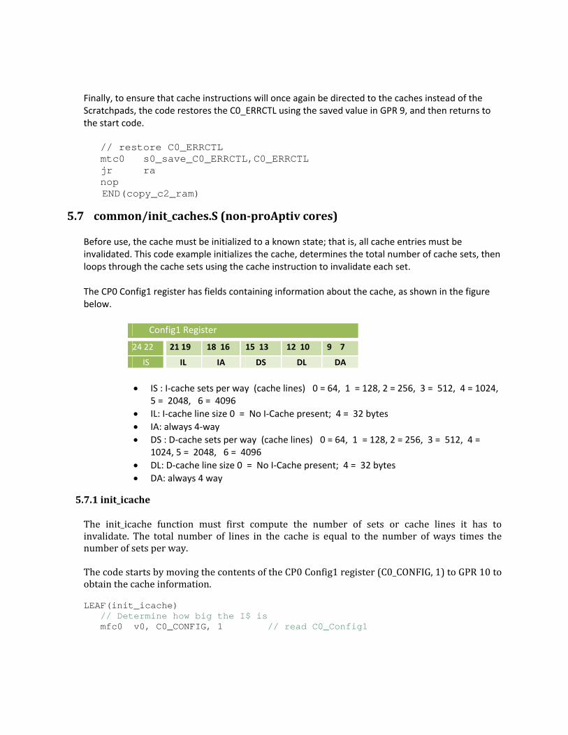
Finally, to ensure that cache instructions will once again be directed to the caches instead of the Scratchpads, the code restores the C0_ERRCTL using the saved value in GPR 9, and then returns to the start code. // restore C0_ERRCTL mtc0 s0_save_C0_ERRCTL,C0_ERRCTL jr ra nop END(copy_c2_ram)
5.7 common/init_caches.S (nonproAptiv cores) Before use, the cache must be initialized to a known state; that is, all cache entries must be invalidated. This code example initializes the cache, determines the total number of cache sets, then loops through the cache sets using the cache instruction to invalidate each set. The CP0 Config1 register has fields containing information about the cache, as shown in the figure below.
Config1 Register
24 22 21 19 18 16 15 13 12 10 9 7
IS IL IA DS DL DA
• IS : I‐cache sets per way (cache lines) 0 = 64, 1 = 128, 2 = 256, 3 = 512, 4 = 1024, 5 = 2048, 6 = 4096
• IL: I‐cache line size 0 = No I‐Cache present; 4 = 32 bytes • IA: always 4‐way • DS : D‐cache sets per way (cache lines) 0 = 64, 1 = 128, 2 = 256, 3 = 512, 4 =
1024, 5 = 2048, 6 = 4096 • DL: D‐cache line size 0 = No I‐Cache present; 4 = 32 bytes • DA: always 4 way
7.1 init_icache The init_icache function must first compute the number of sets or cache lines it has to nvalidate. The total number of lines in the cache is equal to the number of ways times the
5.
inumber of sets per way. The code starts by moving the contents of the CP0 Config1 register (C0_CONFIG, 1) to GPR 10 to obtain the cache information.
LEAF(init_icache) // Determine how big the I$ is mfc0 v0, C0_CONFIG, 1 // read C0_Config1

Next it determines the line size of the I‐cache, using the extract instruction is to extract the line size. It uses the Config1 register value that was saved in general purpose register 10, starting at bit 19, and extracts 3 bits to the least‐significant bits of register 11. // Isolate I$ Line Size ext v1, v0, CFG1_ILSHIFT, 3 The extracted value is tested to see if it is 0; if so, there is no Instruction cache, so it branches ahead without initializing the cache. // Skip ahead if No I$ beq v1, zero, done_icache nop Now the code decodes the line size to get the actual number of bytes in a line. It does this by shifting 2 to the left by the encoded line‐size value. li a2, 2 sllv v1, a2, v1 // Now have true I$ line size in bytes Now the code extracts the number of sets per way from the value read from the Config1 register that was stored in general purpose register 10, using the extract instruction. ext a1, v0, CFG1_ISSHIFT, 3 // extract IS The extracted value is converted to the actual number of sets per way by shifting 64 left by the extracted value. li a2, 64 sllv a0, a2, a0 // I$ Sets per way The number of ways is extracted using the extract instruction starting at bit 16 and extracting 3 bits to the least‐significant bits of register 13. The code then adds one to the value to get the actual number of ways. // Config1IA == I$ Assoc - 1 ext a1, v0, CFG1_IASHIFT, 3 add a1, 1 Now the sets per way are multiplied by the number of ways to get the total number of sets in the cache, which will become the number of initialization loops to be performed. mul a0, a0, a1 // Total number of sets GPR 14 will be used as an index into the cache. It will be set to a virtual address, and then translated to a physical address. Since the address 0x8000 0000 is in KSEG0, the CPU will ignore the top bit, so virtual 0x8000 0000 will become physical address 0x0000 0000. Since the cache is physically indexed, the first time through the loop, the cache instruction will write the tag to way 0, index line 0.

The lui instruction will load 0x8000 into the upper 16 bits and clear the lower 16 bits of the register. lui a2, 0x8000 // Get a KSeg0 address for cache ops Clearing the tag registers does two important things: it sets the Physical Tag address called PTagLo to 0, which ensures the upper physical address bits are zeroed out, and it also clears the valid bit for the set, which ensures that the set is free and may be filled as needed. The code uses the Move to Coprocessor zero instruction to move the general purpose register zero, which always contains a zero, to the tag registers. // Clear TagLo/TagHi registers mtc0 zero, C0_TAGLO // write C0_ITagLo mtc0 zero, C0_TAGHI // write C0_ITagHi The code is almost ready to start the loop through the cache. This move instruction puts the total number of sets that the code computed into register 15, which will be decremented each time through the loop. move a3, a0 The cache instruction will be using the Index Store tag operation on the Level 1 instruction cache so the op field is coded with 8. The first two bits are 00 for the level one instruction cache, and the operation code for Index Store tag is encoded as 010 in bits two, three and four. next_icache_tag: // Index Store Tag Cache Op // Will invalidate the tag entry, clear the lock bit, and clear // the LRF bit cache 0x8, 0(a2) The index type of operation can be used to address a byte in the cache in a specific way of the cache. This is done by dividing the virtual address argument stored in the base register of the cache instruction into several fields.
Unused Way Index Byte Index
13 12 11 5 4 0
The size of the index field will vary according to the size of a cache way. The larger the way, the larger the index needs to be. In the table above, the combined byte and page index is 12 bits, because each way of the cache is 4K. The way number is always the next two bits following the index.

The code does not explicitly set the way bits. Instead it just increments the virtual address by the cache lines size, so that the next time through the loop, the cache instruction will initialize the next set in the cache. Eventually this increment has the effect of setting the cache to index 0 of the next way in the cache, because it overflows into the way bits. Now all the code needs to do is loop maintenance. First decrement the loop counter (15/t7). add a3, -1 // Decrement set counter Then test it to see if it has reached zero, and if not, branch back to label one. bne a3, zero, next_icache_tag The instruction in the branch delay slot, which is always executed, is used to increment the virtual address (14/t6) to the next set in the cache. (11/t3) holds the line size in bytes. add a2, v1 // Get next line address From this point on, the code can be executed from a cached address. This is easily done by changing the return address from a KSEG1 address to a KSEG0 address by simply inserting a 0 into bit 29 of the address. However, if you are debugging, this will confuse the debugger, and you will no longer be able to do source‐level debugging. That is why it is commented out here. Once you have debugged your code, you can uncomment the “ins” line. done_icache: jr ra nop END(init_icache) The function is complete and returns to start.
5.7.2 init_dcache The init_dcache code is very similar to the init_icache code. The main difference is the cache instruction. The cache instruction will be using the Index Store tag operation on the Level 1 data cache, so the op field is coded with a 9. The first two bits are 01 for the Level 1 data cache, and the operation code for Index Store tag is encoded as 010 in bits two, three, and four. The rest of the code is the same as the init_icache and will not be described again.
5.7.3 change_k0_cca This function will change the Cache Coherency Attribute (CCA) of KSEG0 when in Kernel mode. It will turn caching on.

For coherent processor cores (1004K, 1074K, interAptiv and proAptiv), the CCA will be set to 5, which means that the KSEG0 address space will be set to cached write back with write allocate, coherent, and when a read misses in the cache, the line will become shared. For non‐coherent cores (24K, 34K, 74K, and microAptiv), the CCA will be set to 3, which means that the KSEG0 address space will be set to cached write back with write allocate. The code will read the CP0 Config register. Then it will test to see if it is executing on a coherent core. The non‐coherent CCA of 3 is set in the branch delay slot, so that if it isn’t a coherent core, the code will branch around the next instruction at sets the coherent CCA of 5 so if it is not a coherent core the code will fall through and set the CCA to 3. Next it will insert the CCA into the register that holds the Config Register value that was just read and then write it back to the CP0 Config Register. The non‐coherent CCA of 3 is set in the branch delay slot, so that if it isn’t a coherent core, the code will branch around the next instruction that sets the coherent CCA of 5, so if it is not a coherent core, the code will fall through and set the CCA to 3. Next it will insert the CCA into the register that holds the Config Register value that was just read and then write it back to the CP0 Config Register. LEAF(change_k0_cca) // NOTE! This code must be executed in KSEG1 (not KSGE0 uncached) // Set CCA for kseg0 to cacheable mfc0 v0, C0_CONFIG // read C0_Config beqz r11_is_cps, set_kseg0_cca li v1, 3 // CCA for all others li v1, 5 // CCA for coherent cores set_kseg0_cca: ins v0, v1, 0, 3 // insert K0 field mtc0 v0, C0_CONFIG // write C0_Config jr ra nop END(change_k0_cca)
5.7.4 init_l23u First a little background on the larger picture:
• L2 and L3 caches are system resources that are used by all cores in a CPS. Initialization of the L2 and L3 caches is done only by Core 0 in a CPS, because it only needs to be done once.
• The initialization of the L2 and L3 caches can be very time consuming because of their size. The initialization code will execute a lot faster if it is being run out of the instruction cache, so it should be done after the instruction cache has been initialized.
• The instruction cache is a Core resource and not initialized in the System initialization section of the code. Therefore, to be efficient and run the L2 and L3 cache initialization out of the I‐cache, the boot code tries to delay cache initialization until Core resources are initialized and it has checked to make sure it is only initialized by Core 0. This can only be

done if the L2 or L3 caches can be disabled before other cores are released to run this boot code. Otherwise there is a danger that other cores will use the L2 or L3 caches before Core 0 has initialized them.
• The CCA override feature controls the cache attributes for the L2 cache. It allows disabling the L2 cache by enabling the CCA override and setting the CCA to uncached.
• The CCA override works along with the L2 cache implementation. If your CPS uses the current MIPS implementation for the L2 cache, the CCA override feature is supported. However, your system can implement its own version of the L2 that does not support this feature. If that is the case, the L2 and L3 caches must be initialized as a system resource before other cores are released to run.
• MIPS does not have a reference implementation of an L3 cache. If your CPS has an L3 cache and it can be disabled, you will need to add code here to disable it. If it can’t be disabled, it will need to be initialized at this point in the code.
The init_l23u function tries to enable the CCA override and set the L2 cache to uncached in the GCR_BASE register, thus disabling it. On systems that do not support CCA override, writes to the CCA override field have no effect, and reading back the GCR_BASE register will not show the CCA override being set. First the code checks to see if it is executing on a coherent processing system, and if it isn’t, it will branch around the next piece of code and initialize the L2/L3 caches for a non‐coherent system. In this course, only the code for a coherent system will be covered. LEAF(init_l23u) // Use MR2 CCA Override to allow cached execution of L2/3 init. // Check for CCA_Override_Enable by writing a one. beqz r11_is_cps, init_l23 nop The code reads the GCR Base register. lw a0, 0x0008(r22_gcr_addr)// GCR_BASE The next 3 lines of code are used to enable CCA Override and set the L2 cache CCA to uncached. li a3, 0x50 // CM_DEFAULT_TARGET Memory // CCA Override Uncached enabled ins a0, a3, 0, 8 sw a0, 0x0008(r22_gcr_addr) Now the code will read back the GCR_BASE register. If the CCA override bit is set, it means the code above worked, and the L2 cache is set to uncached. If that is the case, the code will skip the initialization for now and be called again later when operating out of the L1 instruction cache. If not, the code will branch to the init_l23 function, which will initialize the L2 and L3 cache.
lw a0, 0x0008(r22_gcr_addr)// GCR_BASE ext a0, a0, 4, 1 // CCA_Override_Enable bnez a0, done_l23 // Skip if CCA Override is implemented. nop b init_l23 nop END(init_l23u)
5.8 init_L23caches.S
5.8.1 Init_l23c The code in this function will be called from start.S after the L1 caches have been initialized. It will check to see if the core implements CCA Override. If it does, it will call the code to initialize the L2 and L3 caches. Recall from the previous section that the code also checks to see if CCA override was implemented, and if it wasn’t, it initialized the L2 and L3 caches while the code was executing in uncached mode,. So there is no need to do it again here.
LEAF(init_l23c)
// Skip cached execution if CCA Override is not implemented. // If CCA override is not implemented the L2 and L3 caches
// would have already been initialized when init_l23u was called. beqz r11_is_cps, done_l23 nop lw a0, 0x0008(r22_gcr_addr)// GCR_BASE bnez r8_core_num, done_l23 // Only done from core 0. ext a0, a0, 4, 1 // CCA_Override_Enable beqz a0, done_l23 nop END(init_l23c)

5.8.2 init_l23 This code initializes the L2 and L3 caches. The init_icache function must first compute the number of sets or cache lines it has to invalidate. The total number of lines in the cache is equal to the number of ways times the number of sets per way. The code starts by moving the contents of the CP0 Config1 register (C0_CONFIG, 1) to GPR 10 to get the cache information. LEAF(init_L23) // Determine how big the I$ is mfc0 v0, C0_CONFIG, 2 // read C0_Config2 Next it determines the line size of the I‐cache, using the extract instruction is to extract the line size. It uses the Config1 register value that was saved in general purpose register 10, starting at bit 4, and extracts 4 bits to the least‐significant bits of register 11. // Isolate I$ Line Size ext v1, v0, 4, 4 Now the code decodes the line size to get the actual number of bytes in a line. It does this by shifting 2 to the left by the encoded line‐size value. li a2, 2 sllv v1, a2, v1 // Now have true L2$ line size in bytes Now the code extracts the number of sets per way from the value read from the Config1 register that was stored in general purpose register 10, using the extract instruction. ext a0, v0, 8, 4 // extract IS The extracted value is converted to the actual number of sets per way by shifting 64 left by the extracted value. li a2, 64 sllv a0, a2, a0 // L2$ Sets per way The number of ways is extracted using the extract instruction starting at bit 0 and extracting 4 bits to the least‐significant bits of register 13. The code then adds one to the value to get the actual number of ways. ext a1, v0, 0, 4 add a1, 1 Now the sets per way are multiplied by the number of ways to get the total number of sets in the cache, which will become the number of loops to be preformed to initialize the cache.

mul a0, a0, a1 // Total number of sets GPR 14 will be used as an index into the cache. It will be set to a virtual address, and then translated to a physical address. Since the address 0x8000 0000 is in KSEG0, the CPU will ignore the top bit, so virtual 0x8000 0000 will become physical address 0x0000 0000. Since the cache is physically indexed, the first time through the loop, the cache instruction will write the tag to way 0 index line 0. The lui instruction will load 0x8000 into the upper 16 bits and clear the lower 16 bits of the register. lui a2, 0x8000 // Get a KSeg0 address for cache ops Clearing the tag registers does two important things: it sets the Physical Tag address called PTagLo to 0, which ensures the upper physical address bits are zeroed out, and it also clears the valid bit for the set, which ensures that the set is free and may be filled as needed. The code uses the Move to Coprocessor zero instruction to move the general purpose register zero, which always contains a zero, to the tag registers. // Clear L2 TagLo/TagHi registers mtc0 zero, C0_TAGLO, 4 // write C0_ITagLo mtc0 zero, C0_TAGLO, 4 // write C0_ITagHi The cache instruction will be using the Index Store tag operation on the Level 2 cache so the op field is coded with B. The first two bits are 11 for the L2 cache and the operation code for Index Store tag are encoded as 010 in bits two, three and four. next_L2cache_tag: // Index Store Tag Cache Op will invalidate the tag entry cache 0xB, 0(a2) Now all the code needs to do is loop maintenance. First decrement the loop counter. add a3, -1 // Decrement set counter Then test it to see if it has gotten to zero, and if not branch back to label one. bne a3, zero, next_icache_tag The instruction in the branch delay slot, which is always executed, is used to increment the virtual address (14/t6) to the next set in the cache. The value in (11/t3) is the line size in bytes. add a2, v1 // Get next line address done_l2cache: // disable CCA Override to enable L2 cache

lw a0, 0x0008(r22_gcr_addr) // GCR_BASE ins a0, zero, 0, 8 // CCA Override disabled sw a0, 0x0008(r22_gcr_addr) // GCR_BASE jr ra nop END(init_L23)
5.9 common/init_caches2.s (proAptiv and interAptiv Cores only) The functions in this file will be used in place of those in init_caches.S. These functions are an example of an implementation‐specific cache initialization. The code assumes specific cache sizes of 32K or 64K, that the environment is multi‐core multiprocessing, and that there an L2 cache. Before it can be used, the cache must be initialized to a known state; that is, all cache entries must be invalidated. This code example initializes the cache, finds the total number of cache sets, then loops through the cache sets using the cache instruction to invalidate each set.
5.9.1 init_icache
LEAF(init_icache) // For this Core there is always a I cache // The IS field determines how may set there are // IS = 2 there are 256 sets // IS = 3 there are 512 sets // v1 set to line size, will be used to increment // through the cache tags li v1, 32 // Line size is always 32 bytes. This core always has a line size of 32 bytes, 4 ways, and can only have a 32 or 64K I‐cache. The IS field (sets per way) of the Config1 register will be use to determine the size of the cache. This field can have one of 2 values: a value of 2 for a 32K cache, or a value of 3 for a 64K cache. mfc0 v0, C0_CONFIG, 1 // Read C0_Config1 ext a3, v0, CFG1_ILSHIFT, 3 // Extract IS li a2, 2 // Used to test against If the check is true, the code uses the branch delay slot, which is always executed, to set the set iteration value to 256 for a 32k cache, and then branchrs ahead to Isets_done. If the check is false, the code still sets the iteration value to 256 in the branch delay slot, but then falls through and sets it again to 512 for a 64K cache. beq a2, a3, Isets_done // if IS = 2 li a3, 256 // sets = 256
li a3, 512 // else sets = 512 Skipped if branch taken

Isets_done: GPR 14 will be used as an index into the cache. It will be set to a virtual address, and then translated to a physical address. Since the address 0x8000 0000 is in KSEG0, the CPU will ignore the top bit, so virtual 0x8000 0000 will become physical address 0x0000 0000. Since the cache is physically indexed, the first time through the loop, the cache instruction will write the tag to way 0 index line 0. The lui instruction will load 0x8000 into the upper 16 bits and clear the lower 16 bits of the register. lui a2, 0x8000 // Get a KSeg0 address for cacheops Clearing the tag registers does two important things: it sets the Physical Tag address (PTagLo) to 0, which ensures the upper physical address bits are zeroed out, and it also clears the valid bit for the set, which ensures that the set is free and may be filled as needed. The code uses the Move to Coprocessor zero instruction to move the general purpose register zero, which always contains a zero, to the tag register. // clear the lock bit, valid bit, and the LRF bit mtc0 zero, C0_TAGLO // Clear C0_ITagLo to invalidate entry The cache instruction will be using the Index Store tag operation on the Level 1 instruction cache, so the op field is coded with 8. The first two bits are 00 for the Level 1 instruction cache, and the operation code for Index Store tag is encoded as 010 in bits two, three, and four. next_icache_tag: cache 0x8, 0(a2) // Index Store tag Cache opt The index type of operation can be used to address a byte in the cache in a specific way of the cache. This is done by dividing the virtual address argument stored in the base register of the cache instruction into several fields:
Way Index Byte Index
14 13 12 5 4 0
The size of the index field will vary according to the size of a cache way. The larger the way, the larger the index needs to be. In the table above, the combined byte and page index is 13 bits, because each way of the cache is 8K. The way number is always the next two bits following the index. The code does not explicitly set the way bits. Instead it just increments the virtual address by the cache lines size, so the next time through the loop the cache instruction will initialize the next set in the cache.

Eventually this increment has the effect of setting the cache to index 0 of the next way in the cache because it overflows into the way bits. Now all the code needs to do is loop maintenance. First decrement the loop counter (12/t4). add a3, -1 // Decrement set counter Then test it to see if it is zero, and if it has not, branch back to label one. bne a3, zero, next_icache_tag // Done yet? The instruction in the branch delay slot, which is always executed, is used to increment the virtual address (14/t6) to the next set in the cache. (11/t3) holds the line size in bytes add a2, v1 // Increment line address by line size From this point on, the code can be executed from a cached address. This is easily done by changing the return address from a KSEG1 address to a KSEG0 address by simply inserting a 0 into bit 29 of the address. However, if you are debugging, this will confuse the debugger and you will no longer be able to do source‐level debugging. That is why it is commented out here. Once you have debugged your code, you can uncomment the “ins” line. done_icache: // Modify return address to kseg0 which is cacheable // (for code linked in kseg1.) // However it make it easier to debug if this is not // done so while Debugging this // this should be commented out ins ra, zero, 29, 1 jr ra nop END(init_icache)
5.9.2 init_dcache The initialization of the D‐cache is very similar to the I‐cache initialization.
LEAF(init_dcache) // For this Core there is always a Dcache // The DS field determines how may set there are // DS = 2 there are 256 sets // DS = 3 there are 512 sets // v1 set to line size, will be used to increment // through the cache tags li v1, 32 // Line size is always 32 bytes.

This core always has a line size of 32 bytes, 4 ways, and can only have a 32 or 64K I‐cache. The IS field (sets per way) of the Config1 register will be use to determine the size of the cache. This field can have one of 2 values: a value of 2 for a 32K cache, or a value of 3 for a 64K cache. mfc0 v0, C0_CONFIG1 // Read C0_Config1 ext a3, v0, CFG1_DSSHIFT, 3 // Extract DS li a2, 2 // Used to test against If the check is true, the code uses the branch delay slot (which is always executed) to set the set iteration value to 256 for a 32k cache, and then branches ahead to Isets_done. If the check is false, the code still sets the iteration value to 256 in the branch delay slot, but then falls through and sets it again to 512 for a 64K cache. beq a2, a3, Dsets_done // if DS = 2 li a3, 256 // sets = 256 li a3, 512 // else sets = 512 Skipped if branch taken Dsets_done: GPR 14 will be used as an index into the cache. It will be set to a virtual address, and then translated to a physical address. Since the address 0x8000 0000 is in KSEG0, the CPU will ignore the top bit, so virtual 0x8000 0000 will become physical address 0x0000 0000. Since the cache is physically indexed, the first time through the loop the cache instruction will write the tag to way 0 index line 0. The lui instruction will load 0x8000 into the upper 16 bits and clear the lower 16 bits of the register. lui a2, 0x8000 // Get a KSeg0 address for cacheops Clearing the tag registers does two important things: it sets the Physical Tag address (PTagLo) to 0, which ensures the upper physical address bits are zeroed out. It also clears the valid bit for the set, which ensures that the set is free and may be filled as needed. The code uses the Move to Coprocessor zero instruction to move the general purpose register zero, which always contains a zero, to the tag register. // clear the lock bit, valid bit, and the LRF bit mtc0 zero, C0_TAGLO, 2 // Clear C0_DTagLo to invalidate entry The cache instruction will be using the Index Store tag operation on the Level 1 data cache, so the op field is coded with 9. The first two bits are 00 for the Level 1 instruction cache, and the operation code for Index Store tag is encoded as 010 in bits two, three and four. next_dcache_tag: cache 0x9, 0(a2) // Index Store tag Cache opt

The index type of operation can be used to address a byte in the cache in a specific way of the cache. This is done by breaking down the virtual address argument stored in the base register of the cache instruction into several fields.
Way Index Byte Index
14 13 12 5 4 0
The size of the index field will vary according to the size of a cache way. The larger the way, the larger the index needs to be. In the table above, the combined byte and page index is 13 bits because each way of the cache is 8K. The way number is always the next two bits following the index. The code does not explicitly set the way bits. Instead it just increments the virtual address by the cache lines size so that the next time through the loop, the cache instruction will initialize the next set in the cache. Eventually this increment has the effect of setting the cache to index 0 of the next way in the cache, because it overflows into the way bits. Now all the code needs to do is loop maintenance. First decrement the loop counter (12/t4). add a3, -1 // Decrement set counter Then test it to see if it has gotten to zero and if not, branch back to label one. bne a3, zero, next_dcache_tag // Done yet? The instruction in the branch delay slot, which is always executed, is used to increment the virtual address (14/t6) to the next set in the cache. (11/t3) holds the line size in bytes. add a2, v1 // Increment line address by line size At this point the D‐cache initialization is done. done_dcache: jr ra nop END(init_dcache)
5.9.3 disable_l23 This core always has an L2 cache and is always part of a CPS. Thus it needs a disable function to disable the L2 and L3 caches while the L1 cache is being initialized.

LEAF(disable_L23) // Use CCA Override to disable the L2 cache // NOTE: If you have an L3 cache, you must add code here // to disable it or initialize it if it can't be disabled. // Disable the L2 cache using CCA override by writing a 0x50 to // the GCR Base register. 0x50 enables the CCA override bit and // sets the CCA to uncached. lw a0, 0x0008(r22_gcr_addr)// Read GCR_BASE li a3, 0x50 // Enable CCA and set to uncached ins a0, a3, 0, 8 // Insert bits sw a0, 0x0008(r22_gcr_addr)// Write GCR_BASE jr ra nop END(disable_L23)
5.9.4 init_L23 This code initializes the L2 and L3 caches. It is very similar to the code that initialized the L1 instruction cache in the init_icache section and will not be covered here.
5.10 common/init_cp0 The init_cp0 code will initialize the Status Register, Watch registers, clear watch exceptions, clear timer exceptions, and set the Cache Coherence Attributes for KSEG0,
5.10.1 Initialize the CP0 Status register
Status Register, CP0 12, 0
31 27 26 25 24 22 21 20 19 18 17 15 8 7 5 4 3 2 1 0
CU RP FR RE MX BEV TS SR NMI 0 CEE IM(7:0) 0 KSU ERL EXL IE
At this point in the boot, the status register should be set as follows:
• ERL set ‐ the processor is running in kernel mode, Interrupts are disabled, the ERET instruction will use the return address held in ErrorEPC instead of EP, and the lower 2 bytes of KUSEG are treated as an unmapped and uncached region.
• BEV set – bootstrap exception mode.
LEAF(init_cp0) // Initialize Status li v1, 0x00400404 // (IM|ERL|BEV)

mtc0 v1, $12 // write C0_Status
5.10.2 Initialize the Watch Registers Next the code will initialize the Watch registers. The Watch registers are undefined following reset and need to be initialized to avoid getting spurious exceptions after the ERL bit is cleared. The code reads the CP0 Config1 register and extracts the WR field, bit 3. If this bit is not set, there are no Watch registers, so the code checks to see if it is equal to 0, and if it is, the code branches forward around the Watch register initialization. // Initialize Watch registers if implemented. mfc0 v0, C0_CONFIG, 1 // read C0_Config1 ext v1, v0, 3, 1// bit 3 (WR) Watch registers implemented beq v1, $0, done_wr The code sets up the initialization value for the Watch Registers in the branch delay slot. This value effectively clears all watch conditions. li v1, 0x7 // Clear I, R and W conditions There are up to 8 Watch Registers. The next 8 segments are all very similar and will initialize up to 8 Watch Registers. Each one begins by writing the initialization value in GPR 11 to the Watch Hi register. // Clear Watch Status bits and disable watch exceptions mtc0 v1, C0_WATCHHI // write C0_WatchHi0 Each Watch Hi register contains an M bit (bit 31) to indicate that there are “more” Watch registers if it is set. Bit 31 is the sign bit for each word, and if set would indicate that the word is a negative value (less than 0). The code reads the Watch Hi register and checks to see if it is greater than or equal to zero (no M bit set) and if it is, the code branches ahead around the remaining Watch register initializations. mfc0 v0, C0_WATCHHI // read C0_WatchHi0 bne zero, v0, done_wr The code uses the branch delay slot to clear the Watch Lo register to clear the Watch for address. mtc0 zero, C0_WATCHLO // write C0_WatchLo0 The remaining 7 segments are very similar to the one just described, so they will be skipped. After the Watch registers are initialized, the code clears the CP0 Cause register. This register indicates the cause of the most recent exception and comes up in an undefined state. In the case of the Watch Register, if the WP bit in the Cause register is set, then after the ERL bit is cleared, it would cause a spurious Watch exception. done_wr: // Clear WP bit to avoid watch exception upon user code entry,

// IV, and software interrupts. mtc0 zero, C0_CAUSE // write C0_Cause: Init AFTER init of WatchHi/Lo
5.10.3 Clear the Compare Register The code clears the CP0 Compare register so that the core will not get a Timer interrupt after the ERL bit is cleared. // Clear timer interrupt. mtc0 zero, C0_COMPARE // write C0_Compare Return; jr ra nop END(init_cp0)
5.11 common/init_gpr.S init_gpr.S will initialize all of the GPR sets in the core. Each Core has at least one GPR set (set 0) and may be implemented with additional shadow sets that can be used while taking an interrupt. The initializing of the GPR registers is not strictly necessary, but may help debug improperly written code where a value is read without being written. The code starts out by setting the default value that it will write to each register. LEAF(init_gpr) li $1, 0xdeadbeef // (0xdeadbeef stands out)
Next the code reads the CP0 Shadow Register set Control register (C0_SRSCtl) and extracts the HSS (Highest shadow Set Number). (On a core with only the base shadow set, this will be set to 0). The code extracts the HSS into GPR 0 of the base register set. The code uses GPR 0 of the base GPR set as a countdown loop counter. At the end of the loop, the code will check to see if this is 0 and exit if it is or decrement it if it is not. mfc0 $29, $12, 2 // read C0_SRSCtl ext C0_ERRPC, $29, 26, 4 // extract HSS Now the code sets uo the core so the wrpgpr (write register previous general purpose register) instruction will write to the shadow set number held in GPR 30. It does this by setting the Previous Shadow Set field (4 bits starting at bit 6) in the Shadow Register Set control register (CP0 29). next_shadow_set: // set PSS to shadow set to be initialized ins $29, $30, 6, 4 // PSS mtc0 $29, C0_SRSCTL // write C0_SRSCtl The wrpgpr instruction is used to initialize the registers. wrpgpr $1, $1

wrpgpr $2, $1 wrpgpr $3, $1 ….. wrpgpr $29, $1 When the code reaches 30, it checks to see if GPR 30 of the base register set is 0. Since it doesn’t want to wipe out the return value held in GPR 31 of the base set, it branches around the setting of registers 30 and 31. // early exit when we get to set 0 so we don't clobber return in ra beqz $30, done_init_gpr nop wrpgpr $30, $1 wrpgpr $31, $1 Then it branches back to the beginning of the loop and subtracts 1 from the shadow set number. b next_shadow_set add $30, -1 The GPR initialization is complete and the code returns to start. done_init_gpr: jr ra nop END(init_gpr)
5.12 common/init_tlb (non proAptiv cores only) init_tlb.S will initialize the Translation Look aside Buffer (TLB) if present. The TLB needs to be initialized so that there are no random translations in it. The code first checks to see if the core has a TLB. It reads the CP0 Config Register (16) and checks the MT (MMU Type) field (3 bits starting at bit 7) by extracting it to GPR 11, then sees if it is set to 1. If it’s not, the core doesn’t have a TLB, so the code will go to the end of the function. LEAF(init_tlb) check_for_tlb: // Determine if we have a TLB mfc0 v1, C0_CONFIG // read C0_Config ext v1, v1, 7, 3 // check MT field li a3, 0x1 // load a 1 to check against bne v1, a3, done_init_tlb In the branch delay slot, the code reads the MMU Size field in the CP0 Config1 register for later use.
mfc0 v0, C0_CONFIG1 // read C0_Config1

At this point the code checks to see if this is an MT core, and if not, it skips ahead to start initializing the TLB. (If you know the core is not an MT core, you can comment out the code from here to the start_init_tlb label.) // Check for TLB sharing between vpe. beqz r10_has_mt_ase, start_init_tlb nop If it is an MT core, then the code checks to see if it is executing on VPE 0 by checking the VPE number that was setup in r9_vpe_num (GPR 17). If it is 0, it skips ahead to start initializing the TLB. beqz r9_vpe_num, start_init_tlb Next the code reads the CP0 MVPControl register (CP0 0 select 1) to see if TLB sharing is turned on by extracting the STLB field (bit 3). If it is, it means it is executing on a VPE other than 0, but since it is sharing the TLB, the TLB has already been initialized by VPE 0, so it can skip to the end of the function. If it is not sharing the TLB, it will fall through and initialize the TLB of VPE 1. mfc0 a0, zero, 1 // read MVPControl ext a0, a0, 3, 1 // extract STLB bnez a0, done_init_tlb // vpe1 but sharing tlb nop Now the code will use the CP0 Config1 value stored earlier in GPR 10 and extract the MMU size field (6 bits starting at bit 25) into GPR 11. This is used as the highest TLB entry and will be used as the first index into the TLB. start_init_tlb: // Config1MMUSize == Number of TLB entries - 1 ext v1, v0, CFG1_MMUSSHIFT, 6 // extract MMU Size Now to clear all entry registers, we initialize all fields in the TLB to 0. To do this we use the same move to Coprocessor zero instruction using general purpose register 0, which always contains the value 0, and move its contents to the corresponding Coprocessor 0 register. mtc0 zero, C0_ENTRYLO0 // write C0_EntryLo0 mtc0 zero, C0_ENTRYLO1 // write C0_EntryLo1 mtc0 zero, C0_PAGEMASK // write C0_PageMask mtc0 zero, C0_WIRED // write C0_Wired Now we load $12 with the address to be placed in the entry. Note that it will be marked invalid but will ensure that the TLB does not have duplicate entries. li a0, 0x80000000 We will now use a loop to initialize each TLB entry.
The next_tlb_entry_pair label in the left column is the label of the start of the loop and the point we will loop back to. To make sure the address that will be written to the TLB entry is unique, the VPE or core number is inserted into it. next_tlb_entry_pair: Previously the code stored the highest numbered TLB entry in general purpose register v1. Here it is used to program the TLB entry index. The code uses the move to Coprocessor 0 instruction to copy the contents of general purpose register v1 to Coprocessor 0 register, which is the index register. The index will indicate the TLB entry to be written. The address to be initialized is written to the CP0 EntryHi register.
mtc0 v1, C0_INDEX // write C0_Index mtc0 a0, C0_ENTRYHI // write C0_EntryHi The code needs to make sure all the writes to CP0 been completed before writing the TLB entry. It does this by using the ehb instruction. ehb Now the TLB Write Indexed Instruction is used to write the TLB entry. tlbwi
The address is incremented by 16K so there are no duplicates. add a0, (2<<13) The branch instruction is used to see if the code has written the last TLB entry (entry 0). Here the code compares the TLB index value that is in general purpose register 11 with 0, and if they are not equal, the code branches back to the top of the loop. bne v1, zero, next_tlb_entry_pair The last instruction is in the branch delay slot and will always be executed. It uses the add instruction to decrement the index value in the general purpose register 11 by adding a ‐1.
add v1, -1
When the loop is finished, the function returns to start. done_init_tlb: jr ra nop END(init_tlb)
5.13 common/init_tlb2 (proAptiv cores only) init_tlb2.S initializes the VTLB and FTLB Translation Look‐aside Buffers. This code example is specific to processors with the VTLB/FTLB feature. In addition, it uses the fact that these cores will always have a least a 64K VTLB, and if they have the optional FTLB, it will always be 512 entries. The TLB needs to be initialized so that there are no random translations in it. LEAF(init_tlb) compute_TLB_size: The MT field in the CP0 Config register (16, 0) is used to decode what type of TLBs are in the Core. If CP0 Config MT = 1, there is only a VTLB and it may be greater than 64K. If CP0 Config MT = 4, there is also an FTLB and the VTLB is 64K. The code reads the CP0 Config register and extracts the MT field. // Determine if we have an FTLB or just a VTLB and set size accordingly mfc0 v1, C0_CONFIG // read C0_Config ext v1, v1, 7, 3 // check MT field A 1 is loaded into GPR 15 to test against. The code checks to see if MT is equal to 1, indicating there is only a VTLB, and sets the VTLB size to 64 in the branch delay slot. If it was not equal to one, the only other value it could be is 4, indicating it has an FTLB, so the code jumps ahead to set the total TLB size with FTLB. li a3, 0x1 // load a 1 to check against bne v1, a3, ftlb // if not only VTLB branch li v1, 64 // set VTLB entries to 64 If the branch falls through, it means that we don’t have an FTLB, but the VTLB may have an extended size (beyond the default 64 entries). The MMUSizeExt field in CP0 config 4 (16, 4) contains 7 bits of extended entries. These bits are the upper 7 bit of the number of total entries in the VTLB. The code reads Config 4 and extracts the MMUSizeExt field. It then shifts this value 7 to the left to put the bits in the correct position. Then it adds the default value of 64 to get the total number of TLB entries. Once the TLB size is determined, the code loads it into GPR v1 that will be used as a loop counter to integrate through and initialize TLB entries and branches to the start of the TLB initialization. mfc0 $15, C0_CONFIG, 4 // Read Config 4 ext a3, a3, 0, 7 // get MMUSizeExt sll a3, a3, 7 // shift to upper bits add v1, v1, a3 // add to the 64 b start_init_tlb nop The code reaches the ftlb label if the MT field was not 1. This means that there is an FTLB. The FTLB is a set size of 512 entries, so the total number of entries is the addition of the 64 VTLB entries plus the 512 FTLB entries or 576. The code loads 576 into GPR v1 that will be used as a loop counter to integrate through and initialize TLB entries.

ftlb: li v1, 576 // set value of 64 + 512 if using FTLB Now to clear all entry registers, we will initialize all fields in the TLB to 0. To do this we use the same move to Coprocessor zero instruction using general purpose register 0, which always contains the value 0, and move its contents to the corresponding Coprocessor 0 register. start_init_tlb: mtc0 zero, C0_ENTRYLO0 // write C0_EntryLo0 mtc0 zero, C0_ENTRYLO1 // write C0_EntryLo1 mtc0 zero, C0_PAGEMASK // write C0_PageMask mtc0 zero, C0_WIRED // write C0_Wired Now we load $12 with the address to be placed in the entry. Note that it will be marked invalid but will ensure that the TLB does not have duplicate entries. li a0, 0x80000000 We will now use a loop to initialize each TLB entry. The next_tlb_entry_pair label in the left column is the label of the start of the loop and the point we will loop back to. To make sure the address that will be written to the TLB entry is unique, the VPE or core number is inserted into it. next_tlb_entry_pair: ins a0, r23_cpu_num, 20, 4 // add "Core" number Previously the code stored the highest numbered TLB entry in general purpose register 11. Here it is used to program the TLB entry index. The code uses the move to Coprocessor 0 instruction to copy the contents of general purpose register 11 to Coprocessor 0 register, which is the index register. The index will indicate the TLB entry to be written. The address to be initialized is written to the CP0 EntryHi register.
mtc0 v1, C0_INDEX // write C0_Index mtc0 $12, C0_ENTRYHI // write C0_EntryHi The code needs to make sure all the writes to CP0 been completed before writing the TLB entry. It does this by using the ehb instruction. ehb Now the TLB Write Indexed Instruction is used to write the TLB entry. tlbwi
The address is incremented by 16K so there are no duplicates.

add a0, (2<<13) The branch instruction is used to see if the code has written the last TLB entry (entry 0). Here the code compares the TLB index value that is in general purpose register 11 with 0, and if they are not equal, the code branches back to the top of the loop. bne v1, zero, next_tlb_entry_pair The last instruction is in the branch delay slot and will always be executed. It uses the add instruction to decrement the index value in the general purpose register 11 by adding a ‐1.
add v1, -1
When the loop is finished, the function returns to start. done_init_tlb: jr ra nop END(init_tlb)
5.14 cps/init_cm.S Coherence manager (CPS systems, 1004K and 1074K only) The code in init_cm.S initializes the Coherence Manager. First the code checks to see if it is booting a coherent processing system, and if not, will branch to the end of this function. LEAF(init_cm) beqz r11_is_cps, done_cm_init // skip if not a CPS nop Register Fields
Name Bits
Global CSR Access Privilege Register (GCR_ACCESS Offset 0x0020)
Reset State
CM_ACCESS_EN 7‐0 Each bit in this field represents a coherent requester. If the bit is set, that requester is able to write to the GCR registers (this includes all registers within the Global, Core‐Local, Core‐Other, and Global Debug control blocks). The GIC is always writable by all requestors. If the bit is clear, any write request from that requestor to the GCR registers (Global, Core‐Local, Core‐Other, or Global Debug control blocks) will be dropped.
0xff
The lower 8 bits of the Global CSR Access Privilege Register controls the write access to the GCR registers by a processor unit (VPE or single core). If a bit is set, the processor unit can change the GCR. Load a 2 into a0. li a0, 2 // mask for cores in this cps. Then the code shifts the 2 to the left by the number of processor units previously stored in r19_more_cores (GPR 19 s3) and then subtracts 1. For example, if there were 4 processor units. then GCR 19 would contain a 3. Then 2 shifted left by 3 is 16 or 10 hex. sll a0, a0, r19_more_cores Now the code subtracts 1. 16 – 1 is 15 or F hex, so now we have all four lower bits set. addiu a0, -1 // Complete mask. These are written to the Global CSR Access Privilege Register, which will now allow all 4 processor units to change the GCR. sw a0, GCR_ACCESS(r22_gcr_addr) // write GCR_ACCESS The code then checks to see if there is an IOCU. It does this by loading the GCR configuration register into GPR 4 and extracting the NUMIOCU field. // Check to see if this CPS implements an IOCU. lw a0, GCR_CONFIG(r22_gcr_addr) // read GCR_CONFIG ext a0, a0, NUMIOCU, NUMIOCU_S // extract NUMIOCU. It then jumps around the next section of code to the end of the init_cm function if there are no IOCUs in the system. beqz a0, done_cm_init If there is an IOCU, then the code will make sure that the CM regions are disabled. The code loads an upper immediate value into a0, which sets bits 16 through 31 and clears bits 0 through 15. The lowest bit, bit 0, set to 0 will disable the CM region. The code uses a0 to store the value to all CM regions and thus disables them. lui a0, 0xffff // Disable the CM regions if there is an IOCU. sw a0, GCR_REG0_BASE(r22_gcr_addr) // write GCR_REG0_BASE sw a0, GCR_REG0_MASK(r22_gcr_addr) // write GCR_REG0_MASK sw a0, GCR_REG1_BASE(r22_gcr_addr) // write GCR_REG1_BASE sw a0, GCR_REG1_MASK(r22_gcr_addr) // write GCR_REG1_MASK sw a0, GCR_REG2_BASE(r22_gcr_addr) // write GCR_REG2_BASE sw a0, GCR_REG2_MASK(r22_gcr_addr) // write GCR_REG2_MASK sw a0, GCR_REG3_BASE(r22_gcr_addr) // write GCR_REG3_BASE sw a0, GCR_REG3_MASK(r22_gcr_addr) // write GCR_REG3_MASK

This completes the CM initialization and the code returns to start. done_cm_init: jr ra nop END(init_cm)
5.15 cps/init_cpc.S Cluster Power Controller (CPS systems, 1004K, 1074K, proAptiv and interAptiv only)
The init_cpc function sets the location of the Cluster Power Controller in the GCR Base Register and stores the address for further use. First the code checks to see if this is a coherent processing system by checking GPR 3 that was set in the beginning. If it’s not, then it will not have a CPC and will skip to the end and return. LEAF(init_cpc) beqz r11_is_cps, done_init_cpc // Skip if non-CPS. nop If there is a CPS, the code checks for a Cluster Power Controller by checking the Cluster Power Controller Status Register. This register is located within the Global Configuration Registers at offset 0xf0. The code uses the previously stored address of the GCR base and the 0xf0 offset to load the value of the Cluster Power Controller Status Register into a0 (GPR 4/a0). There is only one field in the Cluster Power Controller Status Register, called CPC EX, and if that bit is set, then the CPC is connected into the CPS. So all the code needs to do is test it for 0. If it’s 0, there’s no CPC and it branches around this code and returns to the initialization function. In the branch delay slot we ensure GPR 30 is clear to indicate we don’t have a CPC. lw a0, GCR_CPC_STATUS(r22_gcr_addr) // GCR_CPC_STATUS andi a0, 1 beqz a0, done_init_cpc // Skip if no CPC move r30_cpc_addr, zero If there is a CPC, the code will set the address of the CPC in the Cluster Power Controller Base Address Register. The address of the Cluster Power Controller Base Address Register is at offset 88 hex of the GCR. The code uses the known value of the location of CPC is within the system and writes that to the Cluster Power Controller Base Address Register. This is a physical address. Also, bit 0 is set, to enable the address region for the CPC.
li a0, CPC_P_BASE_ADDR // Locate CPC sw a0, GCR_CPC_BASE (r22_gcr_addr) // GCR_CPC_BASE Then the code stores this address for later use in GPR 30 using the KSEG1 equivalent address, and is now done setting up the CPC.

li r30_cpc_addr, CPC_BASE_ADDR // copy to register This completes the CPS initialization and the code returns to start. done_init_cpc: jr ra nop END(init_cpc)
5.16 cps/init_gic.S Global Interrupt Controller (CPS systems, 1004K and 1074K only)
init_gic.S initializes the Global Interrupt controller for this example boot code. The GIC address space is accessed with uncached load and store commands. For each load or store command, the hardware supplies the physical address and the Processor/VPE Number of the requester. The processor/VPE Number is used as an index to reference the appropriate subset of the instantiated control registers. By using the processor/VPE Number information, the hardware writes or reads the correct subset of the control registers pertaining to the “local” Core. Software does not need to explicitly calculate the register index for the “local” Core; it is done entirely by hardware. The GIC is divided into segments: Segment Base
Offset Addressing Method Size
Shared Section 0x0000 Offset relative to GCR_GIC_Base 32K
VPE‐Local Section 0x8000 Offset relative to GCR_GIC_Base + using VPE Number as Index
16K
VPE‐Other Section 0xc000 Offset relative to GCR_GIC_Base + using VPE‐Other Addressing Register as Index
16K
User‐Mode Visible Section
0x10000 Offset relative to GCR_GIC_Base 64K
The Shared segment starts at the Base address of the GIC. This shared section is where the external interrupt sources are registered, masked, and assigned to a particular processing element and interrupt pin. This section is used by all processing elements. Next is the VPE‐local section which starts at the Base address plus 0x8000. This is the section in which interrupts local to a VPE are registered, masked, and assigned to a particular interrupt pin. Using the VPE‐other segment, the “local” CORE can access the registers of another Core by using the Core‐Other address spaces. Software must write the VPE‐Other Addressing Register before accessing these spaces. The value of this register is used by hardware to index the appropriate subset of the control registers for the other core(s).

An additional section called the User‐Mode Visible section is used to give quick user‐mode read access to specific GIC registers. The use of this section is meant to avoid the overhead of system calls to read GIC resources, such as counter registers. First the code checks to see if it needs to initialize the global interrupt controller. It checks GPR 3 and if it is not set, then this is not a Coherent Processing system, so the code will skip the GIC initialization. LEAF(init_gic) beqz r11_is_cps, done_gic // Skip if non-CPS. Nop Even though this is a Coherent Processing System, there still may not be a GIC. To find out, the code reads the Global Control Blocks GIC Status register, offset 0xD0, extracts the GIC_EX bit, and then tests to see if it is set. If it is not set, there is no GIC, so the code will skip the GIC initialization. la a1, GCR_GIC_STATUS + GCR_CONFIG_ADDR lw a0, 0(a1) ext a0, a0, GIC_EX, GIC_EX_S beqz a0, done_gic // If no GIC then skip nop There are two parts of the GIC that need to be initialized: a Shared Part that needs to be initialized by only one core, and a local part that needs to be initialized by each processing unit. This code will do the shared part only if this is core 0, so it checks GPR 23 for the processing unit number and skips the shared section if it is not 0. bnez r23_cpu_num, init_vpe_gic // Only core0 vpe0 nop
5.16.1 Enable the GIC GCR_GIC_BASE Offset 0x0080
Register Fields
Name Bits
Description Read/Write Reset State
GIC_BaseAddress 31‐7
The base address of the 128KB Global Interrupt Controller block
R/W Undefined
GIC_EN 0 Setting to 1 enables GIC R/W 0 As you can see from the table, the address is on a 128K boundary, so the lower 17 bits will always be 0. This leaves space for additional information in the register. The GIC_EN field controls the enabling of the GIC. The code loads the address of the GIC Base Address Register into a1 (GPR 5/a1).

li a1, GCR_CONFIG_ADDR + GCR_GIC_BASE The code loads a0 (GCR 4/a0) with the address of GIC (Physical address). Then bit 0 is set, which enables the GIC. This value is stored to the GCR_GIC_BASE register. li a0, (GIC_P_BASE_ADDR | 1) // Physical address + enable sw a0, 0(a1) Next the code will use the GIC Configuration Register to confirm how many external interrupt sources we have. To do that, the code will read the register and isolate the NUMINTERRUPTS field, bits 16 through 23. Interrupt sources are configured in the core in groups of 8. This field tells you how many groups of 8 minus 1 the core has. The define GIC_SHARED_OFS is the address of the Shared section of the GIC which is loaded into a1 (GPR 5/a1). The Shared Configuration register is located at offset 0. The code loads the value of the register into a0 (GPR 4/a0). // Verify gic is 5 "slices" of 8 interrupts giving 40 interrupts. li a1, GIC_BASE_ADDR // load GIC KSEG0 Address lw a0, GIC_SH_CONFIG (a1) // GIC_SH_CONFIG Then the code extracts the number of interrupt groups. ext a0, NUMINTERRUPTS, NUMINTERRUPTS_S //extract NUMINTERRUPTS For this example, the code loads the expected value of NUMINTERRUPTS into a3 (GPR 7/a3). This example is expecting 40 interrupt sources (4 + 1 times 8). If the code doesn’t get what it expects, it executes a debug breakpoint to stop at a point where you can use the debug probe to see what’s going on. li a3, 4 beq a0, a3, configure_slices nop sdbbp // Failed assertion of 40 interrupts.
5.16.2 Disable interrupts Next the code will disable interrupts for the interrupts used by the example. Register Offset Reset Mask Register numbers Description
0x0300 0 ‐ 31 0x0304 32 ‐ 63 0x0308 64 ‐ 95 0x030c 96 ‐ 127 0x0310 128 ‐159 0x0314 160 ‐ 191
Writing a 0x1 to any bit location masks off (disables) that interrupt. At IP configuration time, the appropriate number of these registers is instantiated to support the number of External Interrupt Sources.

0x0318 192 ‐ 223 0x031c 224 ‐ 255
These are write‐only bits.
To disable interrupts, the code will use the Global interrupt Reset Mask Registers. Each interrupt source has a corresponding bit in a Reset Mask Register. Setting a bit to one resets and disables the interrupt in the GIC. The GIC can control up to 256 interrupt sources. Since all registers in the GIC are 32 bits wide, in order to have enough bits to cover all 256 sources, we will need 8 Reset Mask Registers. The first register will control interrupts 0 through 31, the second set will control 32 through 63, and so on. The system in our example has external interrupts connected to interrupt pins 24 through 39. These interrupt sources will use the first two Global interrupt Reset Mask Registers. The code that follows configures the interrupts one section at a time. First it will configure interrupts 24 through 31 and then 32 through 39. The code disables the first 32 interrupt sources by writing a 1 to bits 24 – 31 in the first Global interrupt Reset Mask Register. The offset of the Global interrupt Reset Mask Registers into the GIC Section is hex 300. configure_slices: // Hardcoded to set up the last 16 of 40 external interrupts // (24..39) for IPI. li a0, 0xff000000 sw a0, GIC_SH_RMASK31_0 (a1) // (disable 0..31)
5.16.3 Setting the Global Interrupt Polarity Registers Similar to the Reset Mask Registers, there is a set of registers that configures the polarity of the interrupt. Register Offset
Interrupt Polarity Register numbers
Description
0x0100 0 ‐ 31 0x0104 32 ‐ 63 0x0108 64 ‐ 95 0x010c 96 ‐ 127 0x0110 128 ‐159 0x0114 160 ‐ 191 0x0118 192 ‐ 223 0x011c 224 ‐ 255
Polarity of the interrupt. For Level Type: 0x0 ‐ Active Low 0x1 ‐ Active High For Single Edge Type: 0x0 ‐ Falling Edge used to set edge register 0x1 ‐ Rising Edge used to set edge register At IP configuration time, the appropriate number of these registers is instantiated to support the number of External Interrupt Sources. These bits are read/write.
The polarity determines how the interrupt is signaled to the core. Interrupts can be level or edge sensitive. If level sensitive, setting the interrupt’s corresponding bit to 1 will configure it active high,

and setting it to 0 will configure it active low. If the interrupt is edge sensitive, setting the corresponding bit to 1 will configure it to interrupt on the rising edge, and setting it to 0 will configure it to interrupt on the falling edge. The offset of the Global interrupt Polarity Registers in the GIC Section is hex 100. The code uses a0 (GPR 4/a0) to write 1’s to bits 24 through 31 of the first interrupt Polarity Register. This configures interrupt sources 24 through 31 to be rising edge sensitive. sw a0, GIC_SH_POL31_0 (a1) // (high/rise 24..31)
5.16.4 Configuring Interrupt Trigger Type There is a set of registers that configures the Trigger type of the interrupt. Setting the corresponding bit causes the interrupt to be treated as Edge signaling; if the bit is cleared, the interrupt is level signaling. The offset of the Global Interrupt Trigger Type Registers in the GIC Section is 0x180. Register Offset
Trigger Type Register numbers
Description
0x0180 0 ‐ 31 0x0184 32 ‐ 63 0x0188 64 ‐ 95 0x018c 96 ‐ 127 0x0190 128 ‐159 0x0194 160 ‐ 191 0x0198 192 ‐ 223 0x019c 224 ‐ 255
Edge or Level triggered 0x0 ‐ Level 0x1 ‐ Edge At IP configuration time, the appropriate number of these registers is instantiated to support the number of External Interrupt Sources. These are read/write bits.
The code uses GPR 4 to write 1’s to bits 24 through 31 of the first interrupt Trigger Register. This configures interrupt sources 24 through 31 to be edge sensitive. sw a0, GIC_SH_TRIG31_0 (a1) // (edge 24..31)
5.16.5 Interrupt Dual Edge Registers There is a set of registers that configures the Edge type if the interrupt is edge signaling. Register Offset
Interrupt Dual Register numbers
Description
0x0200 0 ‐ 31 0x0204 32 ‐ 63 0x0208 64 ‐ 95 0x020c 96 ‐ 127 0x0210 128 ‐159 0x0214 160 ‐ 191 0x0218 192 ‐ 223
Writing a 0x1 to any bit location sets the appropriate external interrupt source to be type dual‐edged. At IP configuration time, the appropriate number of these registers are instantiated to support the number of External Interrupt Sources. These are read/write bits.

0x021c 224 ‐ 255
5.16.6 Interrupt Set Mask Registers There is a set of registers that corresponds to the Global Interrupt Reset Mask registers; these are the Global Interrupt Set Mask Registers. Where the Reset Mask registers disable interrupts, the Set Mask Registers enable interrupts. Register Offset
Interrupt Set Mask Register numbers
Description
0x0380 0 ‐ 31 0x0384 32 ‐ 63
0x0388 64 ‐ 95 0x038c 96 ‐ 127
0x0390 128 ‐159 0x0394 160 ‐ 191 0x0398 192 ‐ 223 0x039c 224 ‐ 255
Writing a 0x1 to any bit location sets the mask (enables) for that interrupt. At IP configuration time, the appropriate number of these registers are instantiated to support the number of External Interrupt Sources. These are write only bits.
Here is the code that sets the interrupt mask. sw a0, GIC_SH_SMASK31_00 (a1) // (enable 24..31) This next section of code configures interrupts 32 through 39 the same way it configured interrupts 24 through 31. The configuration registers that control this range of interrupts is in the second register of each set, so you can see the code is offsetting each register by an additional 4 bytes. Interrupts 32 through 39 are located in the lower 8 bits of the registers, so the code sets GPR 4 to hex ff and will use this register to set interrupt bits 32 through 39, then disable the interrupts, set the Polarity Registers, set the Trigger Register, and then enable the interrupts. li a0, 0xff sw a0, GIC_SH_RMASK63_32(a1) // (disable 32..39) sw a0, GIC_SH_POL63_32(a1) // (high/rise 32..39) sw a0, GIC_SH_TRIG63_32(a1) // (edge 32..39) sw a0, GIC_SH_SMASK63_32(a1) // (enable 32..39)
5.16.7 Map Interrupt to Processing Unit Next the code will configure the Processing unit to which a particular interrupt will be assigned. To do this, the GIC has registers for each interrupt source. Each bit in those registers corresponds to a processing unit in the multi‐core system. Remember that a processing unit can be a VPE in a multi‐threaded, multi‐core system or just a single processor in a multi‐core system. For example, for interrupt source 1 registers, bit 0 would assign the interrupt to core 0 in a single core system or to VPE 0 in an MT system. The current scheme supports up to 64 different processing

units, so there are 2, 32‐bit registers for each interrupt. To allow for future expansion, the registers are spaced 32 bytes apart. Let’s look at the table. Register Offset
Interrupt Map Src to VPE Register numbers
Description
0x2000 Source 0, 0 ‐ 31 0x2004 Source 0, 32 ‐ 63 0x2020 Source 1, 0 ‐ 31 0x2024 Source 1, 32 ‐ 63 0x2040 Source 2, 0 ‐ 31 0x2044 Source 2, 32 ‐ 63 …….. 0x3fe0 Source 255, 0 ‐ 31 0x3fe4 Source 255, 32 ‐ 63
Assigns this interrupt source to a particular VPE. At IP configuration time, the appropriate number of these registers is instantiated to support the number of External Interrupt Sources and the number of VPEs. These are read/write bits.
The Interrupt Map Src to VPE Registers are in the GIC shared section and start at offset 0x2000. The first interrupt has its registers at 2000 and 2004 hex, thus giving it a 64‐bit map area. The next interrupt starts at the start of the section plus 32 bytes or 0x20, so its registers are at 2020 and 2024 hex and so on. There is a convention in MIPS Linux to use the last 16 interrupt sources for inter‐processor interrupts. In the system we are configuring, those are interrupts 24 through 39. The system could contain up to 8 virtual processing units if it is made up of multi‐threaded cores, or 4 physical processing units if it is made up of single‐threaded cores.

This code assigns 2 interrupt sources to each processing unit in the system. It does this using GPR 4 which is set up with a processor unit number. So for VPE 0, a0 (GPR 4/a0) is programmed with a 1. Then the code stores the value in a0 in the appropriate MAP register. In this case, the code divides the interrupt sources into 2 groups, one group from 24 to 31 and the other from 32 through 39. The code will take one interrupt source from each group and program it to a processing unit . For VPE 0, the code uses interrupt 24 and 32. The Map registers for 24 will start at GIC offset 0x2300. The number 0x2300 is obtained by multiplying the interrupt number by the spacing size which is 0x20 and adding the offset for the Global Interrupt Map to VPE Registers which is 0x2000. The code continues until all 8 possible processing units are configured for these interrupts. // Initialize configuration of shared interrupts // Direct GIC_int24..39 to vpe 0..7 // MIPS Linux convention that last 16 interrupts implemented be set // aside for IPI signaling. // (The actual interrupts are tied low and software sends interrupts // via GIC_SH_WEDGE writes.) li a0, 1 // Source 24 to VPE 0
// set bit 0 for CORE0 or for MT vpe0
sw a0, GIC_SH_MAP0_VPE31_0 + (GIC_SH_MAP_SPACER * 24) (a1) // Source 32 to VPE 0 sw a0,GIC_SH_MAP0_VPE31_0+(GIC_SH_MAP_SPACER * 32)(a1) sll a0, a0, 1 // set b// Source 25 to VPE 1
it 1 for CORE1 or for MT vpe1
sw a0,GIC_SH_MAP0_VPE31_0+(GIC_SH_MAP_SPACER * 25)(a1) // Source 33 to VPE 1 sw a0,GIC_SH_MAP0_VPE31_0+(GIC_SH_MAP_SPACER * 33)(a1) sll a0, a0, 1 // set bit 2 for CORE2 or for MT vpe2 // Source 26 to VPE 2 sw a0,GIC_SH_MAP0_VPE31_0+(GIC_SH_MAP_SPACER * 26)(a1) // Source 34 to VPE 2 sw a0,GIC_SH_MAP0_VPE31_0+(GIC_SH_MAP_SPACER * 34)(a1) sll a0, a0, 1 // set bit 3 for CORE3 or for MT vpe3 // Source 27 to VPE 3 sw a0,GIC_SH_MAP0_VPE3// Source 35 to VPE 3
1_0+(GIC_SH_MAP_SPACER * 27)(a1)
sw a0,GIC_SH_MAP0_VPE31_0+(GIC_SH_MAP_SPACER * 35)(a1) sll a0, a0, 1 // set b// Source 28 to VPE 4
it 4 for CORE4 or for MT vpe4
sw a0,GIC_SH_MAP0_VPE31_0+(GIC_SH_MAP_SPACER * 28)(a1) // Source 36 to VPE 4 sw a0,GIC_SH_MAP0_VPE31_0+(GIC_SH_MAP_SPACER * 36)(a1) sll a0, a0, 1 // set bit 5 for CORE5 or for MT vpe5 // Source 29 to VPE 5 sw a0,GIC_SH_MAP0_VPE31_0+(GIC_SH_MAP_SPACER * 29)(a1) // Source 37 to VPE 5 sw a0,GIC_SH_MAP0_VPE31_0+(GIC_SH_MAP_SPACER * 37)(a1) sll a0, a0, 1 // set bit 6 for CORE6 or for MT vpe6

// Source 30 to VPE 6 sw a0,GIC_SH_MAP0_VPE31_0+(GIC_SH_MAP_SPACER * 30)(a1) // Source 38 to VPE 6 sw a0,GIC_SH_MAP0_VPE31_0+(GIC_SH_MAP_SPACER * 38)(a1) sll a0, a0, 1 // set bit 7 for CORE7 or for MT vpe7 // Source 31 to VPE 7 sw a0,GIC_SH_MAP0_VPE3// Source 39 to VPE 7
1_0+(GIC_SH_MAP_SPACER * 31)(a1)
sw a0,GIC_SH_MAP0_VPE31_0+(GIC_SH_MAP_SPACER * 39)(a1)
5.16.8 PerProcessor initialization At this point we have completed initializing the shared section of the GIC. This next section of the code will initialize the per‐processor elements of the GIC. The section of registers being initialized is called VPE‐Local and is located at GIC offset 0x8000.
Register Fields
Name Bits
Description of the Local Interrupt Control Register (GIC_VPEi_CTL) 0x8000
Reset State
FDC_ROUTABLE 4 If this bit is set, the CPU Fast Debug Channel Interrupt is routable within the GIC. If this bit is clear, it is hardwired to one of the SI_Int pins as described by the CORE’s COP0 IntCtlIPFDCI register field.
IP config value
SWINT_ROUTABLE 3 If this bit is set, the CORE SW Interrupts are routable within the GIC. If this bit is clear, it is routed back to the CORE directly.
IP config value
PERFCOUNT_ROUTABLE 2 If this bit is set, the CORE Performance Counter Interrupt is routable within the GIC. If this bit is clear, it is hardwired to one of the SI_Int pins as described by the CORE’s COP0 IntCtlIPPCI register field.
IP config value

TIMER_ROUTABLE 1 If this bit is set, the CORE Timer Interrupt is route‐able within the GIC. If this bit is clear, it is hardwired to one of the SI_Int pins, as described by the CORE’s COP0 IntCtlIPTI register field.
IP config value
EIC_MODE 0 Writing a 1 to this bit will set this VPE local interrupt controller to EIC (External Interrupt Controller) mode. It is a read/write bit.
0
The code reads the Local Interrupt Control Register which is located at offset 0 in the Local section, so it is at GIC location 8000 hex. The code will be using some of the values from this register. init_vpe_gic: // Initialize configuration of per vpe interrupts li a1, (GIC_BASE_ADDR | GIC_CORE_LOCAL_SECTION_OFFSET) lw a3, GIC_COREL_CTL (a1) // GIC_VPEi_CTL
5.16.9 Map Timer interrupt Source The code checks to see if the timer interrupt is routable. It does this by extracting the Timer routable bit from the Control Register value it just read. Then it checks to see if it’s set. If it’s not set, the timer interrupt is not routable and the code will branch around routing it. map_timer_int: // extract TIMER_ROUTABLE ext a0, a3, TIMER_ROUTABLE, TIMER_ROUTABLE_S beqz a0, map_perfcount_int nop

The table below shows the layout of the Registers that will be programmed. Register Fields
Name Bits
Description of the Local WatchDog /Compare/PerfCount/SWIntx Map to Pin Registers
Reset State
MAP_TO_PIN 31 If this bit is set, this interrupt source is mapped to a VPE interrupt pin (specified by the MAP field below). Only one of the MAP_TO_PIN, MAP_TO_NMI, or MAP_TO_YQ bits can be set at any one time. It is a read/write bit.
0x1 for Timer, Perf‐Count and SWIntx; 0x0 for WatchDog
MAP_TO_NMI 30 If this bit is set, this interrupt source is mapped to NMI. Only one of the MAP_TO_PIN, MAP_TO_NMI, or MAP_TO_YQ bits can be set at any one time. It is a read/write bit.
0x1 for WatchDog; 0x0 for Others
MAP_TO_YQ 29 If this bit is set, this interrupt source is mapped to an MT Yield Qualifier pin (specified by the MAP field below). Only one of the MAP_TO_PIN, MAP_TO_NMI, or MAP_TO_YQ bits can be set at any one time. It is a read/write bit.
0
MAP 5:0 When the MAP_TO_PIN bit is set, this field contains the encoded value of the VPE interrupts signals Int[63:0]. The user should only use values of 0 to 5 (decimal). When MAP_TO_YP is set, this field contains the encoded signal selection of the Yield Qualifier.
0
The code sets up a0 (GPR 4/a0) with the encoding used to route the local CORE timer interrupt to the desired processor pin. a0 is written with bit 31 set (MAP_TO_PIN) and a 5 in the Map field to map to pin 5. This will map the local Core’s timer interrupt to the current Processor’s interrupt pin 5. This value is then stored to the GIC Local CORE Timer Map‐to‐Pin Register. li a0, 0x80000005 // Int5 is selected for timer routing sw a0, GIC_COREL_TIMER_MAP(a1) The code checks to see if the Performance Counter interrupt is routable. It does this by extracting the Perfcount Routable bit from the Control Register. Then it checks to see if it’s set. If it’s not set, the performance counter interrupt is not routable and the code will branch around routing it. map_perfcount_int: // extract PERFCOUNT_ROUTABLE ext a0, a3,PERFCOUNT_ROUTABLE, PERFCOUNT_ROUTABLE_S beqz a0, done_gic nop

li a0, 0x80000004 // Int4 is selected for sw a0, GIC_COREL_PERFCTR_MAP (a1) This completes the GIC initialization and the code returns to start. done_gic: jr ra nop END(init_gic)
5.17 cps/join_domain (CPS systems, 1004K,1074K, interAptiv and proAptiv only)
Next the code calls the init function to join this core to the Coherent Domain and the rest of the system. The code first checks to see if this is a Coherent Processing System. If it’s not, it will branch to the end of this function and return. LEAF(join_domain) beqz r11_is_cps, done_join_domain // If CPS then we are done. nop The Core Local Coherence Control Register located at offset 8 within the Core‐Local control block located at 0x2000 of the Global Control Registers controls the entry and exit of a core into the coherent Domain. Bits 0 through 7 represent a coherent requestor within the system. Register Fields
Name Bits
Core Local Coherence Control Register (GCR_Cx_COHERENCE)
Reset State
COH_DOMAIN_EN 7:0 Each bit in this field represents a coherent requester within the CPS. Setting a bit within this field will enable interventions to this Core from that requester. The requestor bit which represents the local core is used to enable or disable coherence mode in the local core. Changing the coherence mode for a local core from 0x1 to 0x0 can only be done after flushing and invalidating all the cache lines in the core; otherwise, the system behavior is UNDEFINED.
0x0

The code sets the first 4 bits of GPR 9 to 1. Then it stores it to the Core Local Coherence Control Register. This enables the other three cores possible in this system to communicate via interventions to this core. // Enable coherence and allow interventions from all other cores. // (Write access enabled via GCR_ACCESS by core 0.) li a0, 0x0f sw a0, (CORE_LOCAL_CONTROL_BLOCK | GCR_CL_COHERENCE) (r22_gcr_addr) ehb Notice the EHB instruction above. This is needed to clear an instruction hazard barrier and make sure the write to the Core Local Coherence Control Registers has taken effect before the code continues. The code initializes GPR 7 which it will use as a loop counter to 0. move a3, zero Next is the loop back label next_coherent_core, which the code will loop back to and join the next core domain. next_coherent_core: The code sets up the Core‐Other Addressing Register, offset 2018 hex from the GCR register base, with the core number it wants to join with. Register Fields
Name Bits
Core‐Other Addressing Register (GCR_Cx_OTHER) Reset State
CoreNum 31:16 CoreNum of the register set to be accessed in the Core‐Other address space.
0x0
It first stores the value of the core into a0 (GPR 4/a0), shifts it into the upper 16 bits, and stores it to the Core‐Other Addressing Register. sll a0, a3, 16 sw a0,(CORE_LOCAL_CONTROL_BLOCK|GCR_CL_OTHER) (r22_gcr_addr) The code now reads the Core Local Coherence Control Register of the other core. Recall how the code set this core’s Core Local Coherence Control Register to enable interventions from other cores, thus entering the domain. The code now needs to wait for the other core to do the same. busy_wait_coherent_core: lw a0,(CORE_OTHER_CONTROL_BLOCK|GCR_CO_COHERENCE) (r22_gcr_addr) beqz a0, busy_wait_coherent_core // Busy wait nop

Once the other core has joined, the code checks to see if there are more cores to wait for and if there are, it branches back to the next coherent core label. It also increments the other core count. bne a3, r19_more_cores, next_coherent_core addiu a3, 1 When all the cores have been waited for, the code returns to start. done_join_domain: jr ra nop END(join_domain)
5.18 cps/release_mp (CPS systems, 1004K, 1074K, interAptiv and proAptiv only)
After the first processor in an MP system has completed the boot code, it can release the remaining processors to execute the boot code. The code checks to see if there are more cores in the system, and if not, it branches to the end of this section and returns. LEAF(release_mp) blez r19_more_cores, done_release_mp // If no more cores done. The code uses a3 (GPR 7/a3) as a counter to decide if it has released all the remaining cores. li a3, 1 The code checks for a Cluster Power Controller by checking if the address was set for the CPC register block. If this value is 0, there is no CPC, and the code will skip ahead and just release the next core so it can begin execution. beqz r30_cpc_addr, release_next_core // If no CPC then use // GCR_CO_RESET_RELEASE nop // else use CPC Power Up command. For systems that have a Cluster Power Controller, only one processor should be powered up when power is first applied. That first processor needs to power up the remaining processors in order for them to continue the boot process. To do that the code will send the power up signal to each of the other cores in the system using the Cluster Power Controller. At offset 0x2010 from the base address of the CPC is the Core‐Other Addressing Register shown here. The code needs to place the number of the other core it wants to power up in this register.

To do this the code moves the number of the core it wants to power up into GPR4. Recall that the first time through, a 1 was stored in a0.
powerup_next_core: // Send PwrUp command to next core causing execution at // their reset exception vector. move a0, a3 Next the code shifts that value to the left into the range of the Core Number field of the Core‐Other Addressing Register. Then that value is stored to the Core‐Other Addressing Register. sll a0, 16 sw a0,(CPS_CORE_LOCAL_CONTROL_BLOCK|CPC_OTHERL_REG)(r30_cpc_addr) Now the code can use the Core‐Other Control Block within the CPC located at offset 0x4000 to control the core whose number it just placed in the Core‐Other Addressing Register. The first register in that block is the CPC Local Command Register. This register is used to power up or down signals for the core. It has a command field called CMD in its first 4 bits. Register Fields
Name Bits
Local Command Register (CPC_CMD_REG) Reset State
CMD 3:0 Requests a new power sequence execution for this domain. Read value is the last executed command.
Code Meaning
4’d3 PwrUp ‐ this domain using setup values in CPC_STAT_CONF_REG. Usable only for Core‐Others access. It is the software equivalent of the SI_PwrUp hardware signal.
0x0
Right now we are interested in powering up the core. That command is 3, so the Code loads a 3 into GPR 4 and stores that register to the address of the CPC at offset 0x4000. This will power up the core and it will begin executing at the reset exception vector, which is the start of this boot code. li a0, PWR_UP // "PwrUp" power domain command. sw a0,(CPS_CORE_OTHER_CONTROL_BLOCK|CPC_CMDO_REG)(r30_cpc_addr) Next the code checks to see if there are any other processors in the system by comparing the current core number with the highest core number that was previously stored in r19_more_cores. If there are other cores, the code loops back to power up the next processor. The processor count is incremented in the branch delay slot. bne r19_more_cores, a3, powerup_next_core

add a3, a3, 1 When all of the processors have been powered up, the function returns to start. jr ra nop The following code is executed in older Coherent Processing Systems without a Cluster Power Controller. When there is no CPC, the cores other than Core0 are held in reset until Core0 releases them. This loop will set the core other value so it can get to the other core’s GCR reset release. release_next_core: // Release next core to execute at their reset exception vector. move a0, a3 sll a0, 16 sw a0,(CORE_LOCAL_CONTROL_BLOCK|GCR_CL_OTHER) (r22_gcr_addr) It then stores a zero to the GCR_CO_RESET_RELEASE register to release that core from reset. sw zero, 0x4000(r22_gcr_addr) // write GCR_CO_RESET_RELEASE It continues looping until all cores are released. bne r19_more_cores, a3, release_next_core add a3, a3, 1 Once all the cores have been released from reset, the code returns to start. done_release_mp: jr ra nop END(release_mp)
5.19 Malta/init_mc_denali (Malta Evaluation Boards Only) The code will initialize the Malta memory controller. It is not covered here since it is unlikely you would be using the same memory controller as a Malta Board.
5.20 Mt/init_vpe1 (mt cores 34K and 1004K only) This code initializes the second VPE of an MT system. It first checks to see if there is an additional TC to bind to a second VPE and then if there is a second VPE. If neither is true, no action is required so the code will jump to the done point. LEAF(init_vpe1) beqz r21_more_tcs, done_init_vpe1 nop

beqz r20_more_vpes, done_init_vpe1 nop To setup the second VPE will require access to some registers that are usually non‐writable. To write to these registers, the code needs to enable Virtual Processor Configuration. This is done by setting the VPC bit in the MVPControl register (CP0 register 0, select 1). The code reads the Register. // This is executing on TC0 bound to VPE0. // Therefore VPEConf0.MVP is set to enter config mode mfc0 v0, C0_MVPCTL // C0_MVPCtl Then it sets the VPC bit (bit 1), or v0, (1 << 1) // M_MVPCtlVPC writes it back to CP0, and executes an ehb to ensure the write has been completed before it continues. mtc0 v0, C0_MVPCTL // C0_MVPCtl ehb Defines are created to make it easier to follow the code. NTCS is a register that will hold the number of TCs in the system, NVPES will hold the number of VPEs in the system, and TC will hold the current number of the TC being initialized. #define a0_NTCS a0 #define a2_NVPES a2 #define a3_TC a3 The MVPConf0 register (CP0 register 0 select 2) holds the number of TCs and VPEs that were configured into the system at build time. The code reads the register. // Get number of TC's and VPE's mfc0 v0, C0_MVPCONF0 // C0_MVPConf0 Then it extracts the highest TC number (total number of TCs ‐1) and the highest VPE number (total number of VPEs ‐1) into the registers noted above. Next it initializes the TC count to 0. ext a0_NTCS, v0, 0, 8 , // extract PTC ext a2_NVPES, v0, 10, 4 // extract PVPE // Initialize TC's/VPE's move TC, zero
nexttc: The next loop will initialize the remaining TCs in the system. The code sets up the target TC field in the VPEControl register (CP0 register 1 select 1). It does this by reading the register, inserting the TC number into the TargTC field, writing it back to the VPE Control register, and executing an ehb to ensure the write took effect before it continues. // Select TC mfc0 v0, C0_VPECTL // read C0_VPECtl ins v0, TC, 0, 8 // insert TargTC mtc0 v0, C0_VPECTL // write C0_VPECtl ehb The code checks to see if the current TC in the loop is TC 0. If it is, it branches forward to the next section since it doesn’t want to re‐initialize itself. // Bind TC to next VPE beqz a3_TC, nextvpe // Don't rebind TC0 nop The TC should be halted before the code starts changing its configuration. To do that, a 1 is placed in GPR 8 and then moved to the C0_TCHalt register (CP0 register 2 select 4). The code executes an ehb to ensure the move has taken effect. // Halt TC being configured li v0, 1 // TCHalt mttc0 v0, C0_TCHALT // C0_TCHalt ehb The code tests to see if this TC is the first TC to be bound to a VPE. If not, it branches to the binding code. This is done because this example sets up only one TC to be executable on each VPE. If there are more TCs than VPEs, the branch will be taken and the TC will be bound to the last VPE in the system (set in the delay slot). slt v1, a2_NVPES, TC // NVPE < TC? bnez v1, 2f // Bind spare TC's to VPElast Now the branch delay slot is used to save the number of VPEs in a2_NVPES. move v1, a2_NVPES // last VPE to bind to Next set this TC to be the only TC runnable on the VPE. For current cores, this effectively sets TC 1 to run exclusively on VPE 1. To do this, the XTC field (bits 21 – 28) in the VPEConf0 register (CP0 register 1 select 2) is set to the TC number. The code reads the VPEConf0 register, inserts the TC number into the XTC field, and writes the register back. // Set XTC for active TC's mftc0 v0, C0_VPECONF0 // read C0_VPEConf0 ins v0, a3_TC, 21, 8 // insert TC -> XTC
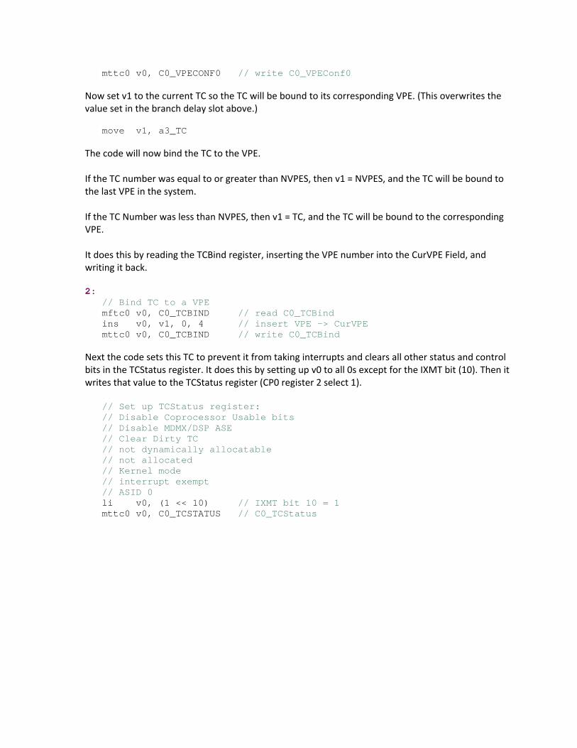
mttc0 v0, C0_VPECONF0 // write C0_VPEConf0 Now set v1 to the current TC so the TC will be bound to its corresponding VPE. (This overwrites the value set in the branch delay slot above.) move v1, a3_TC The code will now bind the TC to the VPE. If the TC number was equal to or greater than NVPES, then v1 = NVPES, and the TC will be bound to the last VPE in the system. If the TC Number was less than NVPES, then v1 = TC, and the TC will be bound to the corresponding VPE. It does this by reading the TCBind register, inserting the VPE number into the CurVPE Field, and writing it back. 2: // Bind TC to a VPE mftc0 v0, C0_TCBIND // read C0_TCBind ins v0, v1, 0, 4 // insert VPE -> CurVPE mttc0 v0, C0_TCBIND // write C0_TCBind Next the code sets this TC to prevent it from taking interrupts and clears all other status and control bits in the TCStatus register. It does this by setting up v0 to all 0s except for the IXMT bit (10). Then it writes that value to the TCStatus register (CP0 register 2 select 1). // Set up TCStatus register: // Disable Coprocessor Usable bits // Disable MDMX/DSP ASE // Clear Dirty TC // not dynamically allocatable // not allocated // Kernel mode // interrupt exempt // ASID 0 li v0, (1 << 10) // IXMT bit 10 = 1 mttc0 v0, C0_TCSTATUS // C0_TCStatus

The code now initializes the TC’s GPR registers using the same method used in init_gpr.S. li v0, 0xdeadbeef // Initialize the TC's register file mttgpr v0, $1 mttgpr v0, $2 mttgpr v0, $3 mttgpr v0, $4 mttgpr v0, $5 mttgpr v0, $6 mttgpr v0, $7 mttgpr v0, $8 mttgpr v0, $9 mttgpr v0, $10 mttgpr v0, $11 mttgpr v0, $12 mttgpr v0, $13 mttgpr v0, $14 mttgpr v0, $15 mttgpr v0, $14 mttgpr v0, $17 mttgpr v0, $18 mttgpr v0, $19 mttgpr v0, $20 mttgpr v0, $21 mttgpr v0, $22 mttgpr v0, $23 mttgpr v0, $24 mttgpr v0, $25 mttgpr v0, $26 mttgpr v0, $27 mttgpr v0, $28 mttgpr v0, $29 mttgpr v0, $30 mttgpr v0, $31

nextvpe: The code checks to see if there any more VPEs to initialize. The code checks to see if the number of VPEs left is less than the number of TCs. If it is, all the VPEs have already been initialized, so the code branches forward to donevpe (where it will check to see if there are any more TCs to initialize). slt v1, a2_NVPES, a3_TC // NVPE < a3_TC? bnez v1, donevpe // No more VPE's nop The code will now initialize the VPE. In fact, on current cores there are at most 2 VPEs, so this code will be executed only if this core has a second VPE. First the code makes sure multi‐threading is disabled. It needs to do this because only one TC should be executing this code at a time. It does this by clearing the TE bit (15) in the VPEControl register (CP0 register 1 select 1). The code reads the register, inserts a 0 into to the bit, and writes the register back. // Disable multi-threading with TC's mftc0 v0, C0_VPECTL // read C0_VPECtl ins v0, zero, 15, 1 // insert TE mttc0 v0, C0_VPECTL // write C0_VPECtl The code checks to see if this is TC 0. If it is, it branches around the initialization to the end of the function, because this has already been done for TC 0. beqz a3_TC, 1f nop The code needs to make sure that no TC is running on the VPE it is initializing. It does this by reading the VPEConf0 (CP0 register 1, select 2) of the VPE it is initializing and inserting a 0 into the VPA Field (Virtual Processor Activated). It also needs to ensure that it is the Master Virtual Processor by setting the MVP bit. This enables the writing of registers associated with the VPE. Then the code writes it back to the VPEConf0 register of the VPE. // For VPE1..n // Clear VPA and set master VPE mftc0 v0, C0_VPECONF0 // read C0_VPEConf0 ins v0, zero, 0, 1 // clear VPA or v0, (1 << 1) // set MVP mttc0 v0, C0_VPECONF0 // write C0_VPEConf0 Next copy the Status register of the running TC to the Status register of the TC being initialized. mfc0 v0, C0_STATUS // read C0_Status mttc0 v0, C0_STATUS // write C0_Status Initialize the Error PC to a dummy value.

li v0, 0x12345678 mttc0 v0, C0_EPC // write C0_EPC Clear the Cause register. mttc0 zero, C0_CAUSE // write C0_Cause Copy the Config register of the running TC to the Status register of the TC being initialized. mfc0 v0, C0_CONFIG // read C0_Config mttc0 v0, C0_CONFIG // write C0_Config The code now puts the Core number into GPR 23 of the TC being initialized. It does this by reading the EBASE register (CP0 register 15, select 1) and extracting the Cpu_num field. Then it copies the CPUNum to the TC’s GPR 23. mftc0 v0, C0_EBASE // read C0_EBASE ext v0, v0, 0, 10 // extract CPUNum mttgpr v0, r23_cpu_num The code programs the TC’s reset vector so that when it is set to run, it will start executing the boot code. It loads the address of the reset_vector from the label created in the linker file. It sets bit 29 to convert the address to a KSEG0 address so it will execute from a cacheable address. Then it writes this value to the TC’s TCRestart register (CP0 2 select 3). // vpe1 of each core can execute cached as it's L1 I$ has // already been initialized. // and the L2$ has been initialized or "disabled" via CCA override. la a1, __reset_vector ins a1, 29, 1 // Convert to cached kseg0 address mttc0 a1, C0_TCRESTART // write C0_TCRestart Now the first thread for this VPE is ready to run, so the code sets it to start running . However, it will not run until all TCs have been initialized and the code exits VPE config mode and enables virtual processing, which is does at the end of this function. The code reads the TCStatus register and enables the TC for handling interrupts by clearing the IXMT bit (10). (This doesn’t really enable interrupts; it just makes it possible for this TC to access them.) It also activates the TC by setting the A bit (13). Then it writes the value to the TC’s TCStatus register. mftc0 v0, C0_TCSTATUS // read TCStatus ins v0, zero, 10, 1 // clear IXMT ori v0, (1 << 13) // set A mttc0 v0, C0_TCSTATUS // write TCStatus Now the code un‐halts the TC by clearing the H field in its TCHalt register. (No other bit needs to be set, so it just clears the whole register.)

mttc0 zero, C0_TCHALT // clear H in TCHalt The code then sets the Virtual Processor Activated (VPA) bit in the VPEConf0 register to activate the VPE and allow the TC it has just initialized to start running. It does this by reading the initialized VPE’s VPEConf0 register and setting the VPA bit, then writing it back. mftc0 v0, C0_VPECONF0 // read VPEConf0 ori v0, 1 // set VPA mttc0 v0, C0_VPECONF0 // write VPEConf0 1: Next the code will check to see if there are any more TCs in the system to initialize. It adds 1 to the current TC being initialized, and then tests to see if it is still within the limits of the number of TCs that are in the system. If it is, it branches back to the top of the loop. donevpe: addu a3_TC, 1 sltu v1, a0_NTCS, TC beqz v1, nexttc nop At this point, all TCs and VPEs have been initialized. The code needs to “Enable Virtual Processing” and take the processor out of “Virtual Processor Configuration” mode. The code will read the MVPCtl register (CP0 register 0 select 1), set the EVP bit (1), and clear the VPC bit. // Exit config mode mfc0 v0, C0_MVPCTL // read MVPCtl ori v0, 1 // set EVP to enable execution by vpe1 ins v0, zero, 1, 1 // VPC mtc0 v0, C0_MVPCTL // write MVPCtl ehb Now for some clean‐up of the code to remove the “//defines” it created in the beginning of this file. #undef a0_NTCS #undef a2_NVPES #undef a3_TC This function is done and returns to start. done_init_vpe1: jr ra nop END(init_vpe1)
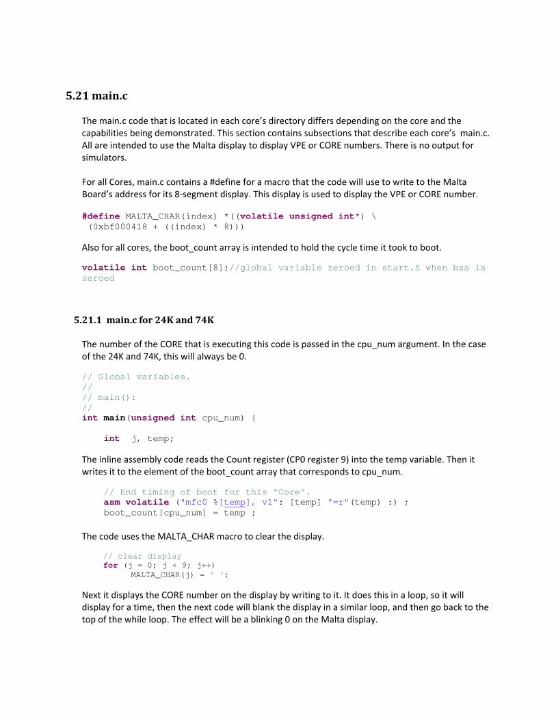
5.21 main.c The main.c code that is located in each core’s directory differs depending on the core and the capabilities being demonstrated. This section contains subsections that describe each core’s main.c. All are intended to use the Malta display to display VPE or CORE numbers. There is no output for simulators. For all Cores, main.c contains a #define for a macro that the code will use to write to the Malta Board’s address for its 8‐segment display. This display is used to display the VPE or CORE number. #define MALTA_CHAR(index) *((volatile unsigned int*) \ (0xbf000418 + ((index) * 8))) Also for all cores, the boot_count array is intended to hold the cycle time it took to boot.
volatile int boot_count[8];//global variable zeroed in start.S when bss is zeroed
5.21.1 main.c for 24K and 74K The number of the CORE that is executing this code is passed in the cpu_num argument. In the case of the 24K and 74K, this will always be 0. // Global variables. // // main(): // int main(unsigned int cpu_num) { int j, temp; The inline assembly code reads the Count register (CP0 register 9) into the temp variable. Then it writes it to the element of the boot_count array that corresponds to cpu_num.
// End timing of boot for this "Core". asm volatile ("mfc0 %[temp], v1": [temp] "=r"(temp) :) ; boot_count[cpu_num] = temp ; The code uses the MALTA_CHAR macro to clear the display. // clear display for (j = 0; j < 9; j++) MALTA_CHAR(j) = ' '; Next it displays the CORE number on the display by writing to it. It does this in a loop, so it will display for a time, then the next code will blank the display in a similar loop, and then go back to the top of the while loop. The effect will be a blinking 0 on the Malta display.
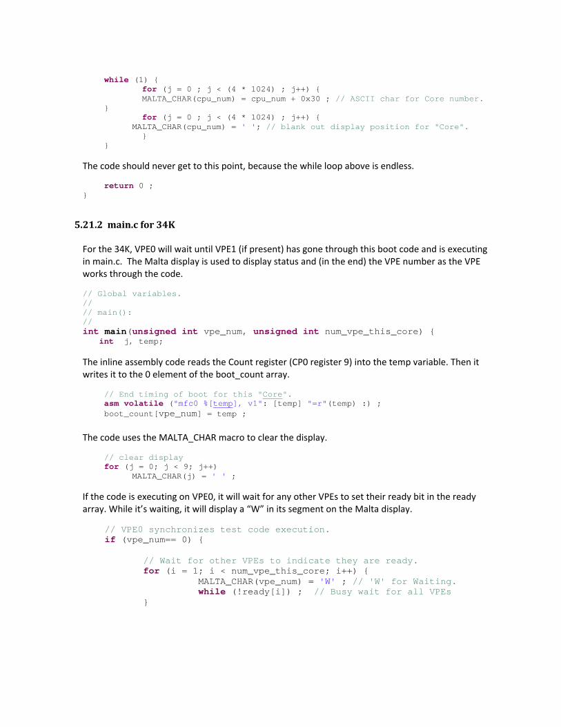
while (1) { for (j = 0 ; j < (4 * 1024) ; j++) { MALTA_CHAR(cpu_num) = cpu_num + 0x30 ; // ASCII char for Core number. } for (j = 0 ; j < (4 * 1024) ; j++) { MALTA_CHAR(cpu_num) = ' '; // blank out display position for "Core". } } The code should never get to this point, because the while loop above is endless. return 0 ; }
5.21.2 main.c for 34K For the 34K, VPE0 will wait until VPE1 (if present) has gone through this boot code and is executing in main.c. The Malta display is used to display status and (in the end) the VPE number as the VPE works through the code. // Global variables. // // main(): // int main(unsigned int vpe_num, unsigned int num_vpe_this_core) { int j, temp; The inline assembly code reads the Count register (CP0 register 9) into the temp variable. Then it writes it to the 0 element of the boot_count array.
// End timing of boot for this "Core". asm volatile ("mfc0 %[temp], v1": [temp] "=r"(temp) :) ; boot_count[vpe_num] = temp ; The code uses the MALTA_CHAR macro to clear the display. clear display // for (j = 0; j < 9; j++) MALTA_CHAR(j) = ' ' ; If the code is executing on VPE0, it will wait for any other VPEs to set their ready bit in the ready array. While it’s waiting, it will display a “W” in its segment on the Malta display. // VPE0 synchronizes test code execution. if (vpe_num== 0) { // Wait for other VPEs to indicate they are ready. for (i = 1; i < num_vpe_this_core; i++) { MALTA_CHAR(vpe_num) = 'W' ; // 'W' for Waiting. while (!ready[i]) ; // Busy wait for all VPEs }

If the code is executing on VPE1, then it will display an “r” (for ready) in its segment of the Malta display and write a 1 to its element of the ready array. The ready array is used in the code above by VPE0. } else { // Other VPE indicates ready and waits... MALTA_CHAR(vpe_num) = 'r' ; // display 'r' for ready. ready[vpe_num] = 1 ; } Both VPEs will now display a “t’. This code is just a place holder, and it’s a good place for you to put test code. // Put test code here: MALTA_CHAR(vpe_num) = 't' ; // 't' for test. Next it displays the VPE number on the display by writing to it. It does this in a loop, so it will display for a time, and then the next code will blank the display in a similar loop and go back to the top of the while loop. The effect will be a blinking 0 on the display. while (1) { for (j = 0 ; j < (4 * 1024) ; j++) { MALTA_CHAR(vpe_num) = vpe_num+ 0x30 ; // ASCII Core number. } for (j = 0 ; j < (4 * 1024) ; j++) { MALTA_CHAR(vpe_num) = ' '; // blank position for "Core". } } The code should never get to this point, because the while loop above is endless. return 0 ; }
5.21.3 main.c for 1074K and proAptiv CPS For the 1074K and proAptiv CPS, Core0 will wait until the remaining CPUs (if present) have gone through this boot code and are executing in main(). All CPUs except CPU0 will wait for an Inter‐processor Interrupt before they continue. CPU0 will just wait until all other CPUs have set their ready element in the ready array. Then CPU0 will continue. All Cores will display their CORE number in their corresponding segment on the Malta display. The set_ipi function will send an interrupt through the Global Interrupt Controller to a specific CORE number provided by cpu_num. The init_gic.S code sets up the GIC to wire each interrupt to a specific CORE. #define FIRST_IPI 32 // GIC interrupts 32+ are used to signal // interrupts between cores.
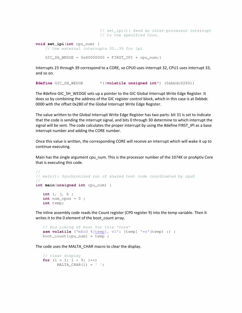
// set_ipi(): Send an inter-processor interrupt // to the specified Core.
void set_ipi(int cpu_num) { // Use external interrupts 32..39 for ipi GIC_SH_WEDGE = 0x80000000 + FIRST_IPI + cpu_num;} Interrupts 23 through 39 correspond to a CORE, so CPU0 uses interrupt 32, CPU1 uses interrupt 33, and so on. #define GIC_SH_WEDGE *((volatile unsigned int*) (0xbbdc0280)) The #define GIC_SH_WEDGE sets up a pointer to the GIC Global Interrupt Write Edge Register. It does so by combining the address of the GIC register control block, which in this case is at 0xbbdc 0000 with the offset 0x280 of the Global Interrupt Write Edge Register. The value written to the Global Interrupt Write Edge Register has two parts: bit 31 is set to indicate that the code is sending the interrupt signal, and bits 0 through 30 determine to which interrupt the signal will be sent. The code calculates the proper interrupt by using the #define FIRST_IPI as a base interrupt number and adding the CORE number. Once this value is written, the corresponding CORE will receive an interrupt which will wake it up to continue executing. Main has the single argument cpu_num. This is the processor number of the 1074K or proAptiv Core that is executing this code. // // main(): Synchronized run of shared test code coordinated by cpu0 // int main(unsigned int cpu_num) { int i, j, k ; int num_cpus = 0 ; int temp; The inline assembly code reads the Count register (CP0 register 9) into the temp variable. Then it writes it to the 0 element of the boot_count array. E g of boot for this "Core" // nd timin asm volatile ("mfc0 %[temp], v1": [temp] "=r"(temp) :) ; boot_count[cpu_num] = temp ;
The code uses the MALTA_CHAR macro to clear the display. clear display // for (i = 1; i < 9; i++) MALTA_CHAR(i) = ' ';

If the code is executing on CPU0, it will wait for any other Cores to set their ready bit in the ready array. While it’s waiting, it will display a “W” in its segment on the Malta display. // cpu0 synchronizes test code execution. if (cpu_num == 0) { num_cpus = num_cores; // Wait for other Cores to indicate they are ready. for (i = 1; i < num_cpus; i++) { MALTA_CHAR(cpu_num) = 'W' ; // 'W' for Waiting. // Busy wait for all Core to be ready. while (!ready[i]) ; } When a core reports it is ready, it will call the wait instruction which will stop the core until the core receives an interrupt. It is CORE 0’s job to send the interrupt to wake up the other cores so they can continue processing. It does this by using inter‐processor interrupts that were set up in the init_gic.S code. The code first changes the segment display by writing an “I” to the corresponding element for the core it is going to interrupt. Then it calls the set_ipi function to send the interrupt. Once CPU0 finishes this loop, it can continue and execute test code and/or the OS. Release other Core to run their tasks. // for (i = 1; i < num_cpus; i++) { // display 'i' for interrupted (from cpu0) MALTA_CHAR(i) = 'i' ; set_ipi(i) ; // Send the ipi } All CPUs other than CORE 0 will halt and wait for CORE 0 to synchronize them. First the code makes sure the interrupt source bit corresponding to its CORE number is cleared by writing to the GIC_SH_WEDGE register. Notice that bit 31 is not set, so this clears any interrupt that might be pending. Then it enables interrupts. } else { // Clear this Core’s IPI source GIC_SH_WEDGE = FIRST_IPI + cpu_num ; // Enable interrupts and wait to be released // via ipi from cpu0 asm volatile ("ei") ; Next each CORE will write an “r” to the segment display to indicate it is ready. Then it will write to the global array to indicate to CORE 0 that it is ready. // Other Core indicates ready and waits... MALTA_CHAR(cpu_num) = 'r' ; // display 'r' for ready. ready[cpu_num] = 1 ; Next interrupts are disabled for the CORE. This avoids any race condition between the testing of the start_test array and the wait instruction. asm volatile ("di") ;

The code will loop, testing its element of the start_test array, and call wait to wait for an interrupt (send by CPU0). while (!start_test[cpu_num]) { // This code will only work reliably if the // WII bit is set in config7. // When this bit is set, any interrupt even // when they are disabled will cause // wait to return. This avoids a race condition. // Wait for interrupt (qualified with "start_test").
asm volatile ("wait") ;
Once an interrupt occurs, the code enables interrupts so its interrupt service routine can run and process the interrupt. The interrupt routine will set the start_test element for this CORE. // enable interrupts so interrupt routine can run the start_test bit // and set asm volatile ("ei") ; asm volatile ("ehb") ; By the time the code gets here, the interrupt routine will have run. The code will disable interrupts before it goes back to the top of the loop. The top of the loop is where the start_test array is checked and just as before, interrupts need to be disabled to avoid a race condition. The start_ array needs to be checked, because any interrupt could have caused termination of the wait instruction. // Disable interrupts again so there is not race // condition between testing the // start_test bit variable and going back to wait. // NOTE for this code we are only expecting IPI that interrupt. //
asm volatile (" di") ; asm volatile ("ehb") ; } } All CPUs will now display a “t’. This code is just a place holder, and it’s a good place for you to put test code. // Put test code here: MALTA_CHAR(cpu_num) = 't' ; // 't' for test. Next it displays the CORE number on the display by writing to it. It does this in a loop, so it will display for a time, and then the next code will blank the display in a similar loop and go back to the top of the while loop. The effect will be a blinking 0 on the display. while (1) { for (j = 0 ; j < (4 * 1024) ; j++) { MALTA_CHAR(cpu_num) = cpu_num + 0x30 ; // cpu } for (j = 0 ; j < (4 * 1024) ; j++) {

MALTA_CHAR(cpu_num) = ' '; // blank out display } } return 0 ; }
5.21.4 main.c for 1004K, interAptiv CPS and interAptivUP
For the 1004K and interAptiv CPS, main() defines a macro that it uses to write to the Malta Board’s address for its 8‐segment display. VPE0 will wait until the remaining VPEs (if present) have gone through this boot code and are executing in main. All VPEs except VPE0 will wait for an interprocessor Interrupt before they continue. VPE0 will just wait until all other VPEs have set their ready element in the ready array. Then VPE0 will continue. All VPEs will display their number in their segment on the Malta display. NOTE: For a CPS, the VPE number will be a combination of the VPE number within a Core and the Core number + 1. For example, VPE0 of Core 0 is numbered 0, and VPE 0 of Core 1 is numbered 2. The set_ipi function will send an interrupt through the Global Interrupt Controller to a specific VPE number provided by cpu_num. The init_gic.S code sets up the GIC to wire each interrupt to a specific VPE. Interrupts 32 through 39 correspond to a VPE, so VPE0 uses interrupt 32, VPE1 interrupt 33, and so on. The #define GIC_SH_WEDGE sets up a pointer to the GIC Global Interrupt Write Edge Register. It does so by combining the address of the GIC register control block, which in this case is at 0xbbdc 0000, with the offset 0x280 of the Global Interrupt Write Edge Register. The value written to the Global Interrupt Write Edge Register has two parts: bit 31 is set to indicate that the code is sending the interrupt signal, and bits 0 through 30 determine which interrupt the signal will be sent to. The code calculates the proper interrupt by using the #define FIRST IPI as a base interrupt number and adding the CPU number. After this value has been written, the corresponding VPE will receive an interrupt that will wake it up to continue executing code where it left off. #define GIC_SH_WEDGE *((volatile unsigned int*) (0xbbdc0280)) #define FIRST_IPI 32 // GIC interrupts 32+ are used to signal interrupts between cores. // // set_ipi(): Send an inter-processor interrupt to the specified VPE. // void set_ipi(int cpu_num) { // Use external interrupts 32..39 for ipi GIC_SH_WEDGE = 0x80000000 + FIRST_IPI + cpu_num ; }

// // main(): Synchronized run of shared test code coordinated by cpu0. // int main(unsigned int cpu_num, unsigned int core_num, unsigned int vpe_num, unsigned int num_vpe_this_core) { int i, j, k ; int num_cpus = 0 ; int temp; The inline assembly code reads the Count register (CP0 register 9) into the temp variable. Then it writes it to the 0 element of the boot_count array. // End timing of boot for this "VPE". asm volatile ("mfc0 %[temp], v1": [temp] "=r"(temp) :) ; boot_count[cpu_num] = temp ; If the code is executing on CPU0 (VPE0), it waits for each core to report the number of VPEs on a core. The code tallies the number of VPEs each core reports in num_cpus, which it will use a little later in this loop. // cpu0 synchronizes test code execution. if (cpu_num == 0) { // Tally number of "VPEs" there are in this CPS. for (i = 0; i < num_cores; i++) { while (!vpe_on_core[i]) { } // Busy wait for core to report number of vpe. num_cpus += vpe_on_core[i]; } It will wait for any other VPEs to set their ready bit in the ready array. While it’s waiting, it will display a “W” in its segment on the Malta Display. // Wait for other VPEs to indicate they are ready. for (i = 1; i < num_cpus; i++) { MALTA_CHAR(cpu_num) = 'W' ; // 'W' for Waiting. // Busy wait for all VPEs to be ready. while (!ready[i]) ; } When a VPE reports it is ready, it will call the wait instruction, which will stop the VPE until the VPE receives an interrupt. It is VPE 0’s job to send the interrupt to wake up the other cores so they can continue processing. It does this by using inter‐processor interrupts that were set up in the init_gic.S code. The code first changes the segment display by writing an “I” to the corresponding element for the core it is going to interrupt. Then it calls the set_ipi function to send the interrupt. Once CPU0 finishes this loop, it can continue and execute test code and/or the OS. // Release other VPE to run their tasks.
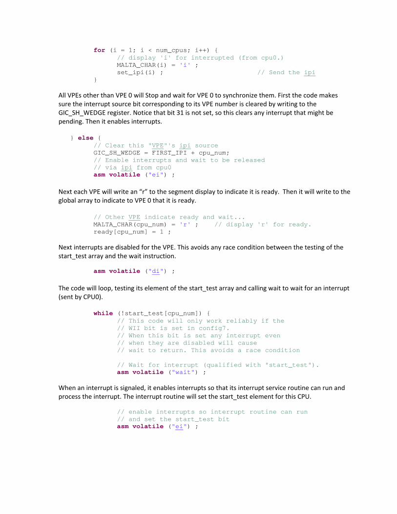
for (i = 1; i < num_cpus; i++) { // display 'i' for interrupted (from cpu0.) MALTA_CHAR(i) = 'i' ; set_ipi(i) ; // Send the ipi } All VPEs other than VPE 0 will Stop and wait for VPE 0 to synchronize them. First the code makes sure the interrupt source bit corresponding to its VPE number is cleared by writing to the GIC_SH_WEDGE register. Notice that bit 31 is not set, so this clears any interrupt that might be pending. Then it enables interrupts. } else { // Clear this "VPE"'s ipi source GIC_SH_WEDGE = FIRST_IPI + cpu_num; // Enable interrupts and wait to be released v// ia ipi f asm volatile ("ei") ;
rom cpu0
Next each VPE will write an “r” to the segment display to indicate it is ready. Then it will write to the global array to indicate to VPE 0 that it is ready. // Other VPE indicate ready and wait... MALTA_CHAR(cpu_num) = 'r' ; // display 'r' for ready. ready[cpu_num] = 1 ; Next interrupts are disabled for the VPE. This avoids any race condition between the testing of the start_test array and the wait instruction. asm volatile ("di") ;
The code will loop, testing its element of the start_test array and calling wait to wait for an interrupt (sent by CPU0). while (!start_test[cpu_num]) { // This code will only work reliably if the // WII bit is set in config7. // When this bit is set any interrupt even // when they are disabled will cause // wait to return. This avoids a race condition // Wait for interrupt (qualified with "start_test").
asm volatile ("wait") ;
When an interrupt is signaled, it enables interrupts so that its interrupt service routine can run and process the interrupt. The interrupt routine will set the start_test element for this CPU. // enable interrupts so interrupt routine can run // and set the start_test bit asm volatile ("ei") ;

By the time the reaches this point, the interrupt routine will have run. The code will disable interrupts before it returns to the top of the loop. The top of the loop is where the start_test array is checked and just as before, interrupts need to be disabled to avoid a race condition. The start_ array needs to be checked because any interrupt could have terminated the wait instruction. // Disable interrupts again so there is no race // condition between testing the // start_test bit variable and going back to wait. // NOTE: for this code we are only expecting an interprocessor interrupt. // asm volatile ("di") ; } } All CPUs will now display a “t’. This code is just a place holder, and it’s a good place to put your test code. // Put test code here: MALTA_CHAR(cpu_num) = 't' ; // 't' for test. Next it displays the VPE number on the display by writing to it. It does this in a loop, so it will display for a time, then the next code will blank the display in a similar loop and go back to the top of the while loop. The effect will be a blinking 0 on the Malta display. while (1) { for (j = 0 ; j < (4 * 1024) ; j++) { MALTA_CHAR(cpu_num) = cpu_num + 0x30 ; // VPE } for (j = 0 ; j < (4 * 1024) ; j++) { MALTA_CHAR(cpu_num) = ' '; // blank out display } } return 0 ; }
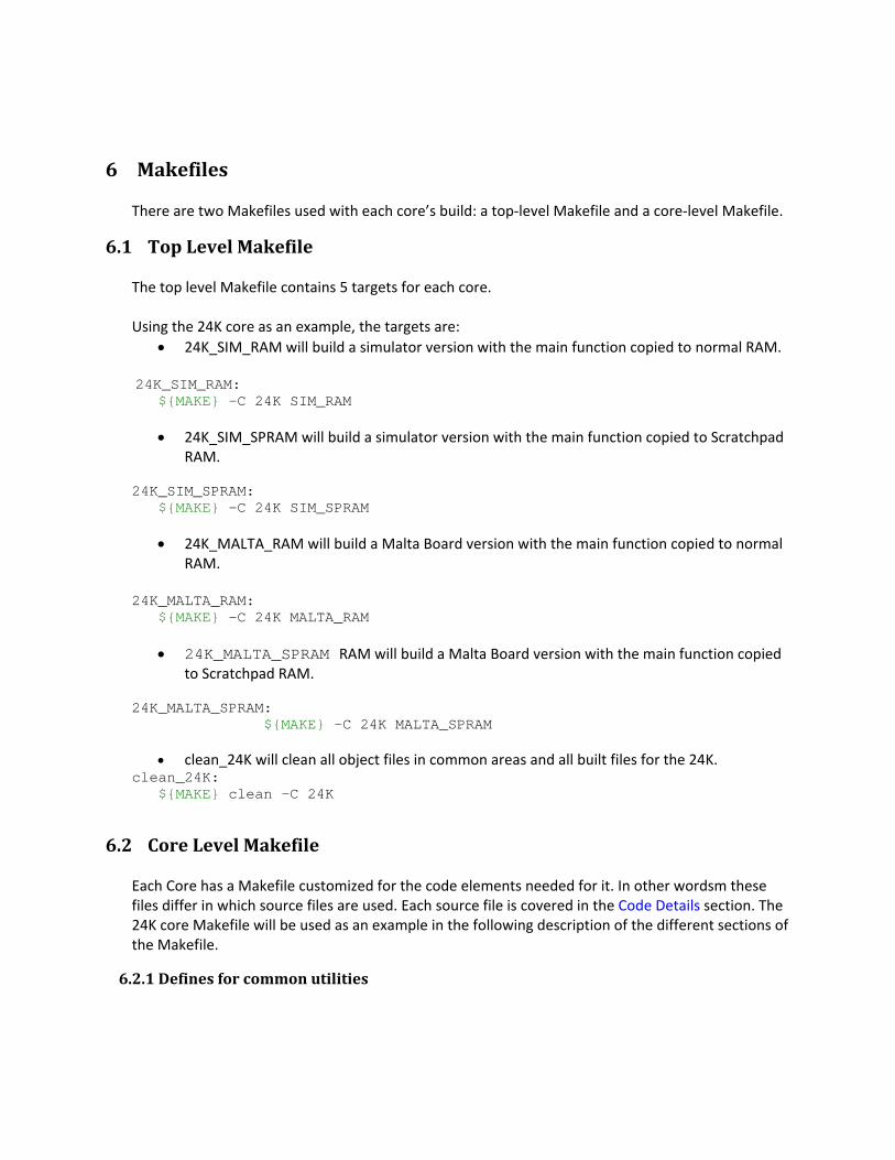
6 Makefiles There are two Makefiles used with each core’s build: a top‐level Makefile and a core‐level Makefile.
6.1 Top Level Makefile The top level Makefile contains 5 targets for each core. Using the 24K core as an example, the targets are:
• 24K_SIM_RAM will build a simulator version with the main function copied to normal RAM. 24K_SIM_RAM: ${MAKE} -C 24K SIM_RAM
• 24K_SIM_SPRAM will build a simulator version with the main function copied to Scratchpad RAM.
24K_SIM_SPRAM: ${MAKE} -C 24K SIM_SPRAM
• 24K_MALTA_RAM will build a Malta Board version with the main function copied to normal RAM.
24K_MALTA_RAM: ${MAKE} -C 24K MALTA_RAM
• 24K_MALTA_SPRAM RAM will build a Malta Board version with the main function copied to Scratchpad RAM.
24K_MALTA_SPRAM:
${MAKE} -C 24K MALTA_SPRAM
• clean_24K will clean all object files in common areas and all built files for the 24K. clean_24K: ${MAKE} clean -C 24K
6.2 Core Level Makefile Each Core has a Makefile customized for the code elements needed for it. In other wordsm these files differ in which source files are used. Each source file is covered in the Code Details section. The 24K core Makefile will be used as an example in the following description of the different sections of the Makefile.
6.2.1 Defines for common utilities
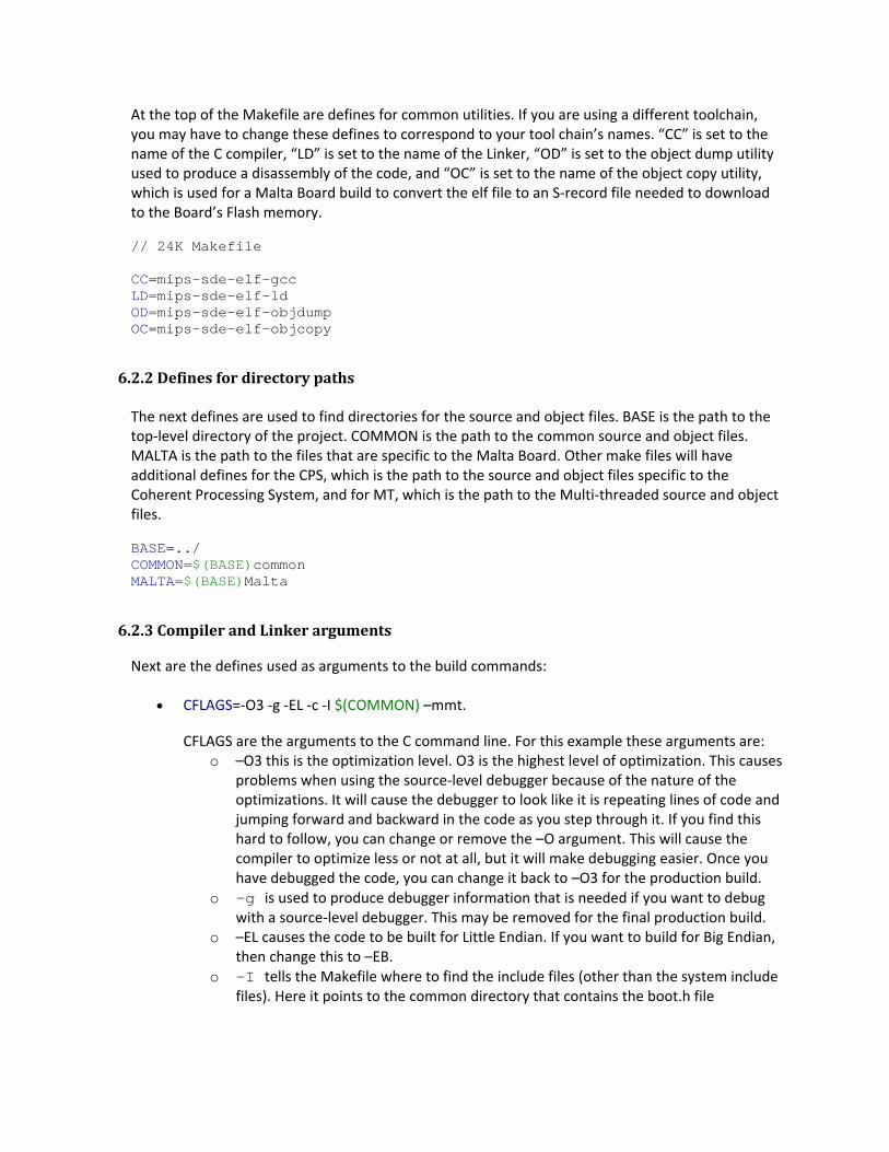
At the top of the Makefile are defines for common utilities. If you are using a different toolchain, you may have to change these defines to correspond to your tool chain’s names. “CC” is set to the name of the C compiler, “LD” is set to the name of the Linker, “OD” is set to the object dump utility used to produce a disassembly of the code, and “OC” is set to the name of the object copy utility, which is used for a Malta Board build to convert the elf file to an S‐record file needed to download to the Board’s Flash memory. // 24K Makefile
CC=mips-sde-elf-gcc LD=mips-sde-elf-ld OD=mips-sde-elf-objdump OC=mips-sde-elf-objcopy
6.2.2 Defines for directory paths The next defines are used to find directories for the source and object files. BASE is the path to the top‐level directory of the project. COMMON is the path to the common source and object files. MALTA is the path to the files that are specific to the Malta Board. Other make files will have additional defines for the CPS, which is the path to the source and object files specific to the Coherent Processing System, and for MT, which is the path to the Multi‐threaded source and object files.
BASE=../ COMMON=$(BASE)common MALTA=$(BASE)Malta
6.2.3 Compiler and Linker arguments Next are the defines used as arguments to the build commands:
• CFLAGS=‐O3 ‐g ‐EL ‐c ‐I $(COMMON) –mmt. CFLAGS are the arguments to the C command line. For this example these arguments are:
o –O3 this is the optimization level. O3 is the highest level of optimization. This causes problems when using the source‐level debugger because of the nature of the optimizations. It will cause the debugger to look like it is repeating lines of code and jumping forward and backward in the code as you step through it. If you find this hard to follow, you can change or remove the –O argument. This will cause the compiler to optimize less or not at all, but it will make debugging easier. Once you have debugged the code, you can change it back to –O3 for the production build.
o –g is used to produce debugger information that is needed if you want to debug with a source‐level debugger. This may be removed for the final production build.
o –EL causes the code to be built for Little Endian. If you want to build for Big Endian, then change this to –EB.
o –I tells the Makefile where to find the include files (other than the system include files). Here it points to the common directory that contains the boot.h file

o –mmt tells the compiler to use MT instructions. This should only be present for multi‐threaded cores.
• LDFLAGS_SIM_RAM=-T sim_Ram.ld -EL -nostdlib -Wl,-Map=sim_Ram_map • LDFLAGS_SIM_SPRAM=-T sim_SPRam.ld -EL -nostdlib -Wl,-
Map=sim_SPRam_map • LDFLAGS_MALTA_RAM=-T malta_Ram.ld -EL -nostdlib -Wl,-
Map=malta_Ram_map • LDFLAGS_MALTA_SPRAM=-T malta_SPRam.ld -EL -nostdlib -Wl,-
Map=malta_SPRam_map There are several LDFLAG defines, one for each type of build:
o –T is used to pass the name of the linker script file to the linker. There will be more information on the linker script in the next section.
o –EL links for Little Endian. To link for Big Endian, change this to –EB. o –nostdlib tells the linker to not use standard libraries. The boot code does not
support standard library calls (like printf). By using the –nostdlib option, the linker will report an error if a standard library call is made.
o ‐Wl,‐Map=<MAP file Name> this option tells the linker to produce a Map file with the given name. The map file is useful in determining to which addresses the linker has linked the code and data.
6.2.4 Source file lists There are several source file lists that correspond to different builds:
• ASOURCES is a list of the assembly files common to all targets in this Makefile. The list differs from core to core depending on the source needed to boot that particular core.
• MALTASOURCES is a list of assembly files that are specific to a Malta Board build. • ASOURCES_SP is used to combine common sources with a specific source to build for the
Scratchpad RAM version. • ASOURCES_RAM is used to combine common sources with a specific source to build for the
non‐Scratchpad RAM version. • CSOURCES is a list of C source files in the build.
6.2.5 Object file lists The object file lists are built using built‐in make rules that convert the source file lists into object file lists. There is a corresponding OBJECT file define for each source file list.
• MALTAOBJECTS=$(MALTASOURCES:.S=.o) • COBJECTS=$(CSOURCES:.c=.o) • AOBJECTS=$(ASOURCES:.S=.o) • AOBJECTS_SP=$(ASOURCES_SP:.S=.o) • AOBJECTS_RAM=$(ASOURCES_RAM:.S=.o)

The object file lists will be used in the different target builds.
6.2.6 Adding to CFLAGS for Malta Board Builds In order to have a more generic start.S file, the code contains a #define for the Denali memory controller present on Malta boards. For Malta Board target builds, the define “DENALI” needs to be added to the CFLAGS. ifeq ($(findstring MALTA_, $(MAKECMDGOALS)), MALTA_) CFLAGS += -DDENALI Endif To do this, the Makefile built‐in command “findstring” is used to search the target name passed to the make command (MAKECMDGOALS) for MALTA_. If it finds it, it adds –DDENALI to the CFLAGS define.
6.2.7 Make Targets As discussed previously, there are four make targets for each core.
6.2.7.1 MALTA_SPRAM This target builds for a Malta Board using Scratchpad RAM: MALTA_SPRAM : $(COBJECTS) $(AOBJECTS_SP) $(MALTAOBJECTS) $(OC) malta_SPRam.elf -O srec malta_SPRam.rec perl $(COMMON)/srecconv.pl -ES L malta_SPRam This target depends on the common C objects (COBJECTS), the Scratchpad‐specific Assembly objects (AOBJECTS_SP), and the Malta Board‐specific objects (MALTAOBJECTS):
$(CC) $(LDFLAGS_MALTA_SPRAM) $(COBJECTS) $(AOBJECTS_SP)\ $(MALTAOBJECTS) -o malta_SPRam.elf
The CC rule line will build the malta_SPRam.elf executable file using the object lists and Linker flags appropriate to the Malta and Scratchpad build.
$(OD) -d -S -l malta_SPRam.elf > malta_SPRam_dasm The OD rule will produce a disassembly file. $(OC) malta_SPRam.elf -O srec malta_SPRam.rec perl $(COMMON)/srecconv.pl -ES L malta_SPRam

The last two lines use object copy and a perl script to convert the elf file into a flashable file called malta_SPRam.fl.
6.2.7.2 MALTA_RAM This rule differs from the previous one by using object lists, a linker file script, and output names to produce a Malta Board RAM version of the flash file (malta_RAM.fl). MALTA_RAM : $(COBJECTS) $(AOBJECTS_RAM) $(MALTAOBJECTS) $(CC) $(LDFLAGS_MALTA_RAM) $(COBJECTS) $(AOBJECTS_RAM) \ $(MALTAOBJECTS) -o malta_Ram.elf $(OD) -d -S -l malta_Ram.elf > malta_Ram_dasm $(OC) malta_Ram.elf -O srec malta_Ram.rec
perl $(COMMON)/srecconv.pl -ES L malta_Ram
6.2.7.3 SIM_RAM This rule will produce an elf file which is suitable to be used with a simulator with normal RAM.
SIM_RAM : $(COBJECTS) $(AOBJECTS_RAM)
The rule depends on the C objects (COBJECTS) and the Assembly Objects for RAM (AOBJECTS_RAM).
$(CC) $(LDFLAGS_SIM_RAM) $(COBJECTS) $(AOBJECTS_RAM) -o sim_Ram.elf
The CC rule uses the linker script and object file list appropriate to build a Simulator RAM version of the elf file sim_Ram.elf.
$(OD) -d -S -l sim_Ram.elf > sim_Ram_dasm
The OD rule produces a disassembly file from the elf file.
6.2.7.4 SIM_SPRAM This rule differs from the SIM_RAM rule by using objects lists, a linker file script, and output name to produce a Simulator Scratchpad version of the elf file sim_SPRam.elf.
6.2.8 C and Assembly rules These rules will build the objects file needed for the CC rule from the dependency list for the target. .c.o:
$(CC) $(CFLAGS) $< -o $@

The .c.o rule takes an object name from the provided object list and compiles it from the same‐ named file ending in .c instead of .o. .S.o:
$(CC) $(CFLAGS) $< -o $@
The .S.o rule takes an object name from the provided object list and assembles it from the same‐ named file ending in .S instead of .o.
6.2.9 Clean rule The clean rule removes all traces of files produced from all target builds. It does this by using the shell commands listed in the clean rule.
7 Linker scripts The linker scripts are used by the linker to locate the code properly during the link step. They also provide symbols that are used in the boot code to perform the copy from flash memory to RAM or SPRAM. There are four linker scripts per core, one for each make target. All linker scripts use 0x9fc0 0000 as the starting address of the boot code. This is a KSEG0 address that mirrors the KSEG1 boot exception vector address, 0xbfc0 0000, in all MIPS systems, i.e., the memory location of the first instruction that will be fetched. The difference between using a KSEG0 address and a KSEG1 address is that KSEG1 is a non‐cached memory region whereas KSEG0 is a cacheable region that first starts out as uncached and can then be switched to cacheable. (The switch is done after the I‐cache has been initialized in start.S.)
7.1 Malta_Ram.ld This linker script is used in the MALTA_RAM target builds for a Malta Board with a copy of the main code from flash to normal RAM.
_monitor_flash = 0xbe000000 ; .text_init 0x9fc00000 :
AT( _monitor_flash )
The script tells the linker to create a symbol called _monitor_flash with a value of the address of the monitor flash on the Malta board, which is the starting address of the Malta Board’s flash. The Malta Board is setup to alias the normal boot vector, 0xbfc0 0000, to this address. The .text_init 0x9fc0 0000 : gives the linker the starting address for linking the object files that follow. The “AT” command directs the linker to load the code at the _monitor_flash address. Thus the code will be linked to execute starting at the boot vector, but will be loaded into the flash at the

_monitor_flash address, which on the Malta Board also appears to the VPE as the boot exception vector 0xbfc0 0000. The next part of the linker script is a list of object files that will be linked into the .text_init section. Here is an example of the list for a 24K core: { _ftext_init = ABSOLUTE(.) ; /* Start of init code. */ start.o(.text) /* Reset entry point */ ../common/init_gpr.o(.text) set_gpr_boot_values.o(.text) ../common/init_cp0.o(.text) ../common/init_tlb.o(.text) ../Malta/init_mc_denali.o(.text) ../common/init_caches.o(.text) ../common/copy_c2_ram.o(.text) . = ALIGN(8); _etext_init = ABSOLUTE(.); /* End of init code. */ } = 0 This list is the main reason there are different sets of linker scripts for each Core, i.e., because each Core can have a different set of object files. The list for the 24K is the smallest subset of objects files. The other Cores will have a superset of object files, depending on the code that needs to be included to boot that Core. There are two symbols, _ftext_init and _etext_init, that are set in accordance with the list of object files. These are seen in the section above in the beginning and end of the list:
_ftext_init = ABSOLUTE(.) ; /* Start of init code. */
_ftext_init is a symbol that is set to the current link location. In this case, that location is 0x9fc0 0000, because the symbol is at the start of the text_init section (0x9fc0 0000).
_etext_init = ABSOLUTE(.); /* End of init code. */
_etext_init is the symbol set to the last link location of the text_init section. The next part of the script will be used to link and load any object files not in the above list. This happens to be the main.o file for this boot code. The code in main.o will be copied from flash to some type of RAM, so it will be loaded at a flash location but linked for a RAM location. Along the way it will create symbols that will be used by the copy code to copy the code from flash to RAM.
_zap1 = _etext_init - _ftext_init + _monitor_flash;
The _zap1 symbol will be computed at link time. This is the address where main.o code will be loaded into the flash and be used by the copy code as a starting address for the source of the copy to RAM. It is computed by taking the starting address of the monitor flash (_monitor_flash) and adding the difference between the start of the text_init section (_ftext_init) and the ending address

of the text_init section (_etext_init). In other words, the _zap1 symbol is computed as the starting address of the flash plus the size of the text_init section.
.text_ram 0x80100000 : AT( _zap1 )
The .text_ram line tells the linker to link the text_ram section to the 0x8010 0000 RAM address. The AT line tells the linker to load it into memory at the address in the symbol _zap1. { _ftext_ram = ABSOLUTE(.) ; /* Start of code and read-only data */ *(.text)*(.text.*) . = ALIGN(8); _etext_ram = ABSOLUTE(.); /* End of code and read-only data */ } = 0 The above line tells the linker what goes into the text_ram section. First it sets the _ftext_ram symbol to point to the current link address, which in this case is the start of the text_ram section. The code will use this address as the starting destination address for the copy. Next the *(.text) line tells the linker what to put into this section. The .text sections from any object files on the linker command line (in the Makefile) that are not specifically named will go into the .text_ram output section. In the above code, the . = ALIGN(8); aligns the end of the section to an 8‐byte boundary. The _etext_ram symbol is set to the end of the text_ram section. The next section covers the initialized data section. It contains external variables that are initialized in the code.
_zap2 = _etext_ram - _ftext_ram + _zap1 ;
The _zap2 symbol is computed to contain the load address of the next section (data). It is computed by taking the end load address of the text_init, _zap1 and adding the difference between the first address of the text_ram section, _ftext_ram, and the ending address, _etext_ram. In other words, _zap2 equals the ending load address of the first section text_init and the size of the next section text_ram.
.data _etext_ram : AT( _zap2 )
Next the .data line tells the linker where to link the .data section. Here it is set to _etext_ram, which is the ending link address of the last section, text_ram. The AT line tells the linker where to load the data section. This is going to be an address in RAM. The next part describes what’s in the data section.

{ _fdata_ram = ABSOLUTE(.); /* Start of initialised data */ *(.rodata) *(.rodata.*) *(.data) . = ALIGN(8); _gp = ABSOLUTE(. + 0x7ff0); /* Base of small data */ *(.lit8) *(.lit4) *(.sdata) . = ALIGN(8); _edata_ram = ABSOLUTE(.); /* End of initialised data */ } Once again the symbols for the beginning and end link points for the section are set up (_fdata_ram and _edata_ram). In between these symbols is the list of subsections that go into the data section. It also sets up the Global Pointer symbol. This data area is 64K, with the _gp symbol pointing to the middle of it, so address offsets will be no larger than 16 bits plus or minus the Global pointer. This fits with the number of bits allowed for the offset field of instructions like sw. The _gp will be written to GPR $28 before the code in main() is called.
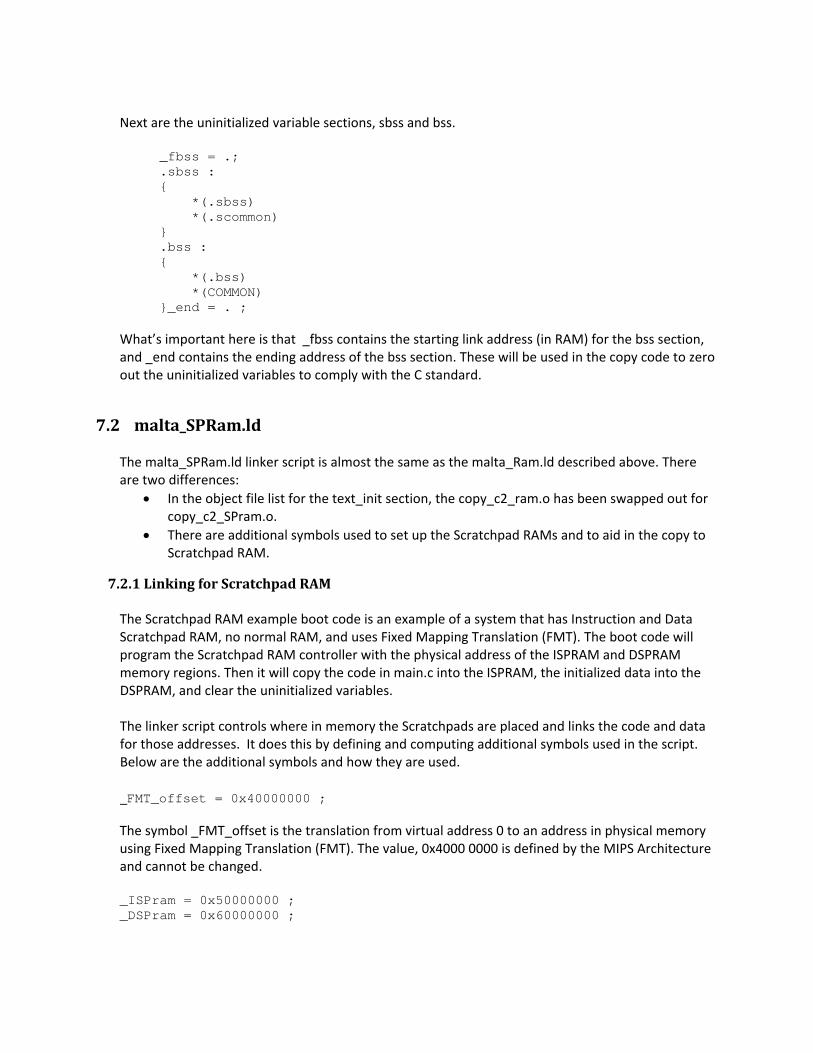
Next are the uninitialized variable sections, sbss and bss.
_fbss = .; .sbss : { *(.sbss) *(.scommon) } .bss : { *(.bss) *(COMMON) }_end = . ;
What’s important here is that _fbss contains the starting link address (in RAM) for the bss section, and _end contains the ending address of the bss section. These will be used in the copy code to zero out the uninitialized variables to comply with the C standard.
7.2 malta_SPRam.ld The malta_SPRam.ld linker script is almost the same as the malta_Ram.ld described above. There are two differences:
• In the object file list for the text_init section, the copy_c2_ram.o has been swapped out for copy_c2_SPram.o.
• There are additional symbols used to set up the Scratchpad RAMs and to aid in the copy to Scratchpad RAM.
7.2.1 Linking for Scratchpad RAM The Scratchpad RAM example boot code is an example of a system that has Instruction and Data Scratchpad RAM, no normal RAM, and uses Fixed Mapping Translation (FMT). The boot code will program the Scratchpad RAM controller with the physical address of the ISPRAM and DSPRAM memory regions. Then it will copy the code in main.c into the ISPRAM, the initialized data into the DSPRAM, and clear the uninitialized variables. The linker script controls where in memory the Scratchpads are placed and links the code and data for those addresses. It does this by defining and computing additional symbols used in the script. Below are the additional symbols and how they are used. _FMT_offset = 0x40000000 ; The symbol _FMT_offset is the translation from virtual address 0 to an address in physical memory using Fixed Mapping Translation (FMT). The value, 0x4000 0000 is defined by the MIPS Architecture and cannot be changed. _ISPram = 0x50000000 ; _DSPram = 0x60000000 ;

The symbols _ISPram and _DSPram are the physical address where the Scratchpad RAM will be located in the system. They will be used by the code in the common/copy_c2_SPram.S to position the Scratchpad RAMs in the physical memory map. These are not fixed addresses. They can be changed, usually to a physical address in the KUSEG region. _code_start = _ISPram - _FMT_offset ; _data_start = _DSPram - _FMT_offset ; The symbols _code_start and _data_start will be used as the starting link addresses for the code and data in main.c. These are computed by using the difference between the start of the SPRam and the _FMT_offset. The difference in these 2 physical addresses translates into a virtual address in KUSEG. .text_ram _code_start : .data _data_start : The address for the SPRAM computed above is used as the link address for the text_ram and data sections.
7.3 sim_Ram.ld and sim_SPRam The only differences in these two linker scripts from their Malta counterparts is the value of the _monitor_flash symbol. Recall the Malta board has flash that starts at 0xbe0 0000, which is aliased to the boot exception vector at 0xbfc0 0000. There is no aliasing done in the simulators, so _monitor_flash has the value of the boot exception vector 0xbfc0 0000.

8 Downloading to the Malta Boot Flash To download the boot code to the Malta Board, attach a parallel cable between the Malta Board and your PC. Configure your PC’s parallel port for printing. Open the “malta_Ram.ld” file in a editor. On Windows, use the WordPad editor. Be sure that “Print Page Numbers” is turned off in the “Page setup”:

Next flip the PROG switch on the S5 switch block to PROG. You should see the display change to “Flash DL”.
Then click on print. The download should be very fast for this example code, because it is very small. “FINISHED” is displayed when the printing is complete:
Flip the PROG switch back and the system should boot. If it doesn’t boot, power cycle the board.

9 Debugging Using NavigatorICS This section covers setting up a Debug session for single, multi‐threaded, and multiprocessor Cores. NavigatorICS version 2.8.2 or newer is required.
9.1 Single Core or first Core of a Multi Thread or Multi Core system This setup will start a debug session that resets the Core or CPS, sets the PC to the reset vector (0xBFC0 0000), and suspends execution. If you are using a Malta Board with an FPGA, you will need to increase the connection time‐out before you can debug. Go to the “Window” menu at the top of the Workspace View and select Preferences ‐> C/C++ ‐>Debug ‐>GDB MI, and increase the “Debugger timeout (MS):”. You can experiment, but it’s safe to just add a 0 to the end. NOTE: The debugger needs to come up once before in order for the “GDB MI” selection to appear in the menu (see figure below), so you might need to start a debug session and have it fail before you can change this value.
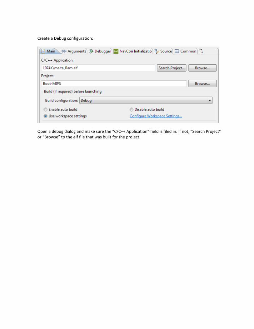
Create a Debug configuration:
Open a debug dialog and make sure the “C/C++ Application” field is filed in. If not, “Search Project” or “Browse” to the elf file that was built for the project.
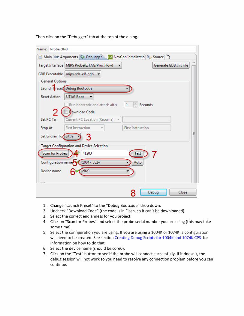
Then click on the “Debugger” tab at the top of the dialog.
1. Change “Launch Preset” to the “Debug Bootcode” drop down. 2. Uncheck “Download Code” (the code is in Flash, so it can’t be downloaded). 3. Select the correct endianness for you project. 4. Click on “Scan for Probes” and select the probe serial number you are using (this may take
some time). 5. Select the configuration you are using. If you are using a 1004K or 1074K, a configuration
will need to be created. See section Creating Debug Scripts for 1004K and 1074K CPS for information on how to do that.
6. Select the device name (should be core0). 7. Click on the “Test” button to see if the probe will connect successfully. If it doesn’t, the
debug session will not work so you need to resolve any connection problem before you can continue.

8. If you are using a singl‐ core system, just click on “Debug” to save the script and start your debug session. For 34K, 1004K, 1074K, interAptiv, and proAptiv systems, continue with the next steps.

Debugging additional VPE (34K, 1004K, and interAptiv): To debug the second VPE you need to create another and slightly different Debug configuration. Here are the changes you need to make:
1. Select “Advanced” for “Launch Preset” 2. The “Reset Action” should be “No Reset” 3. Select “Custom PC/Symbol” and enter the boot vector address for “Set PC to” 4. For “Stop At” select “First Instruction” or in newer versions of NavigatorICS “Don’t Resume” 5. Pick the correct “Device name”
You shouldn’t have to “Scan for Probes” or run the Test; otherwise, this Dialog should look the same. Create a debug configuration for all VPEs in your system.
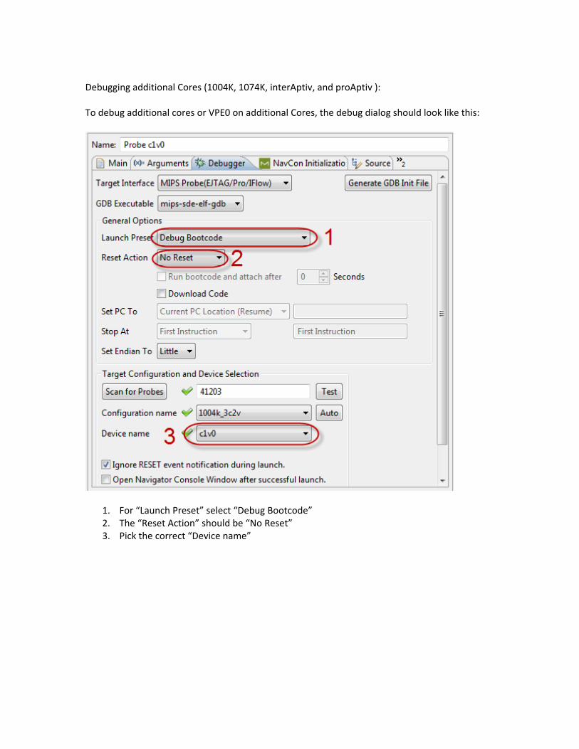
Debugging additional Cores (1004K, 1074K, interAptiv, and proAptiv ): To debug additional cores or VPE0 on additional Cores, the debug dialog should look like this:
1. For “Launch Preset” select “Debug Bootcode” 2. The “Reset Action” should be “No Reset” 3. Pick the correct “Device name”

9.2 Setting Breakpoints in ReadOnly flash code To set breakpoints in code located in read‐only memory, you need to use hardware breakpoints. Do this by right‐clicking in the grey column next to the instruction line you want to break on and select “Toggle Hardware Breakpoints”.
You will see a check in the column:
Selecting the “Breakpoints” tab will show that the breakpoint is a hardware breakpoint.
NOTE: There are a limited number of hardware breakpoints, and the debugger does not tell you when you have run out, so you may need to delete old breakpoints after they have been hit.

9.3 Stopping at main() Once you complete debugging your boot code, you can reconfigure the debug session to stop at main() instead of at the first instruction. This is not as straightforward as it would seem. To stop at main(), the debugger will default to setting a software breakpoint when it starts up. In this example, the main code is being copied from flash to RAM, which will overwrite the software breakpoint and the debugger will not stop at main. The solution is to get the debugger to set a hardware breakpoint instead. In the Debug dialog select “Additional GDB Commands”. In the “Additional Postload Commands” text box enter:
set mem inaccessible‐by‐default off mem 0x10000000 0x10000007 ro
NOTE: If you change the linker script to link main at a different address, the address for the “mem” line above will also need to be adjusted.

9.4 Debugging Multithreaded and Multicore systems When debugging Multi‐threaded or Multi‐core systems, you need to be aware of when a thread or additional core is ready to run before you can initiate a debug session for it. Always start the first core for a multi‐core system and the first core’s first VPE in an MT multi‐core system. Then you need to pick a spot in your code when additional cores or VPEs are at the point where they are ready to run so you can start them. For this boot code example (1004K): Start the first Core:
At the start of the boot code, you will only see the code in the assembler view. This is because the code has been linked for the KSEG0 address 0x9fc0 0000. This address mirrors the boot vector at 0xbfc0 0000. However, the debugger has no reference to this address to correlate with the linked source code, so you will see” No source available” in the source window. You will need to step through the next few instructions in instruction single‐step mode before you will see source code in the source window.
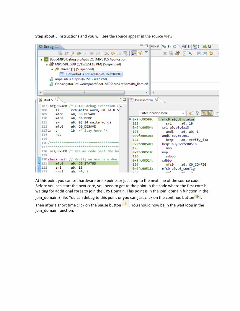
Step about 3 instructions and you will see the source appear in the source view:
At this point you can set hardware breakpoints or just step to the next line of the source code. Before you can start the next core, you need to get to the point in the code where the first core is waiting for additional cores to join the CPS Domain. This point is in the join_domain function in the
join_domain.S file. You can debug to this point or you can just click on the continue button .
Then after a short time click on the pause button . You should now be in the wait loop in the join_domain function:


Now you can start all other cores (not the second VPEs yet). Each debug session for each core will stop at the boot exception vector:
You can debug each core by selecting its thread in the “Debug” pane. After you have finished
debugging each core, select continue for all debug sessions. The display on the Malta Board will show Core 1 and 2 are ready:

If you pause Core 1 or 2 at this point, you will see they are in main().
1. Here is where the “r” gets displayed. 2. Here is the wait loop where the core waits to receive an interrupt. When the interrupt is
received, the start_test[cpu_num] will be set and the core will continue. At this point, If you are working with a multi‐threaded multi‐Core system, all cores have setup their VPE1s to start executing, and you can now start their debug sessions:


At this point you can debug the remaining VPEs form the beginning of the boot code. You will also notice that the Malta display has changed:
You can now see the “W” for Core 0 displayed. If you pause Core 0, you will see it is in this section of code:
Core 0 is waiting for all other processing units to report they have gotten the IPI interrupt.
After you have debugged the remaining VPEs, you can let all debug sessions continue . The display will change:
The display should continue to blink the processor numbers indefinitely.
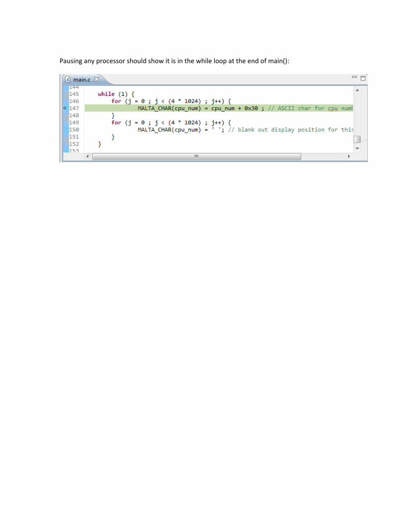
Pausing any processor should show it is in the while loop at the end of main():

1.
10 Creating Debug Scripts for 1004K and 1074K CPS Before you can create a debug configuration for the 1004K and 1074K systems, you need to create debug scripts. You will need to use the Navigator Console. Select “Start Navigator Console and select script” from your Start menu. On Windows it looks like this:

The “Select script” dialog will come up:
1. Select “mips_1004K.tcl” if you want to configure for a 1004K, or “mips_1074K.tcl” if you want to
configure for a 1074K. 2. In the “New name for script file:” text box complete the name of the script file you are creating.
For this example, _2V_2TC.tcl was added because the example configures for a 2‐VPE and 2‐TC system. The name is whatever you want it to be, but it must end in .tcl.
3. Once that’s done, click on “Setup”

The Dialog will change:
1. Select the “Number of CPUs” that you have in your FPGA or Chip. 2. Select the “Number of VPEs per CPU:” that you have in your FPGA or Chip. (NOTE: For a 1074K,
you will not have this choice.) 3. For “Ordering of devices in the jtag chain” choice 2 will be correct for most systems. 4. If you have your probe connected between your computer and board and the board is powered
up, you can select “Save and Run Script” to test to see if the script is correct. If it is, you should get no errors. If you get errors, you have chosen something wrong in the first 3 steps, and you will need to redo the setup with correct values.
Now that when you have created the script, you will see it in the drop‐down for “Configuration name” under the “Debugger” tab in your “Debug dialog”.
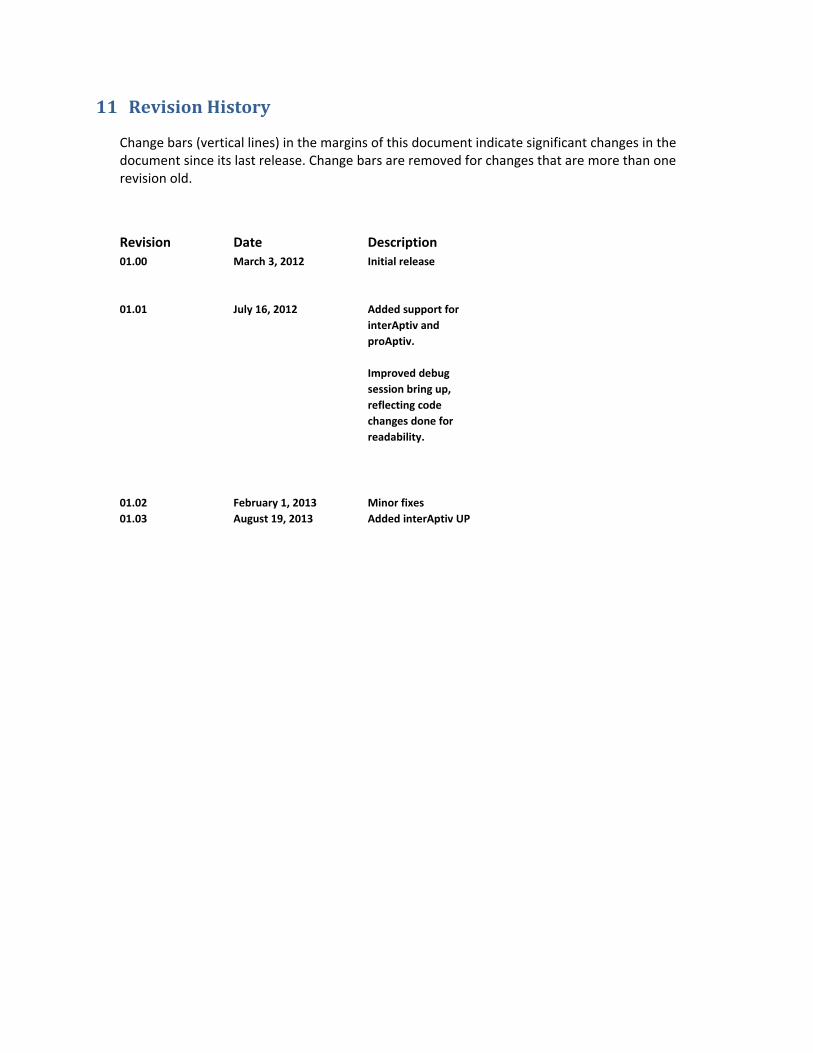
11 Revision History
Change bars (vertical lines) in the margins of this document indicate significant changes in the document since its last release. Change bars are removed for changes that are more than one revision old.
Revision Date Description 01.00
March 3, 2012
Initial release
01.01 July 16, 2012 Added support for interAptiv and proAptiv. Improved debug session bring up, reflecting code changes done for readability.
01.02 01.03
February 1, 2013 August 19, 2013
Minor fixes Added interAptiv UP