bluetooth hci oem module - penguin.czutx/zaurus/datasheets/hwmod/bluetooth/em_datasheet...registered...
TRANSCRIPT

nical Datasheet
Bluetooth HCI OEM Module
Electrical & MechacB-OHCI406i-04, cB-0921-02

2
Copyright © 2008 connectBlue AB.
The contents of this document can be changed by connectBlue AB without prior notice and do not constitute any binding undertakings from connectBlue AB. connectBlue AB is not responsible under any circumstances for direct, indirect, unexpected damage or consequent damage that is caused by this document.
All rights reserved.
Release: 2009-03
Document version: 1.2
Document number: cBProduct-0810-07 (5)
Printed in Sweden.
Trademarks
Registered trademarks from other companies are: Bluetooth is a trademark owned by the Bluetooth SIG, Inc., Microsoft™, Windows™, Windows NT™, Windows 2000™, Windows CE™, Windows ME™, are registered trademarks from Microsoft Corporation.

Section 1.1 - Introduction.Overview
3
Contents
1 Introduction 4 1.1 Overview ............................................................................................4 1.2 Key features.......................................................................................4 1.3 Product Variants ................................................................................5 1.4 Block Diagram cB-OHCI406 ..............................................................6
2 Electrical Interface and Connectors 7 2.1 Overview ............................................................................................7 2.2 Pin Numbering ...................................................................................8 2.3 J1 solder land Description..................................................................9 2.4 Characteristics .................................................................................13
3 Antennas 16 3.1 Surface Mounted Antenna (Internal)................................................16
4 Mounting Information 17 4.1 Board Outlines .................................................................................17 4.2 Using the J6 PCB solder pads.........................................................19 4.3 Antenna Issues ................................................................................19
5 Bluetooth Information 20 5.1 General Information .........................................................................20 5.2 Bluetooth qualification information...................................................21
6 Regulatory Information 22 6.1 Declaration of Conformity ................................................................22 6.2 IC and FCC Compliance for cB-OHCI406i-04 .................................23 6.3 UL listing information .......................................................................25 6.4 Compliance with RoHS directive .....................................................25
7 Guidelines for Efficient and Safe Use 26 7.1 General ............................................................................................26 7.2 Product Care....................................................................................26 7.3 Radio Frequency Exposure .............................................................26 7.4 Electronic Equipment .......................................................................27 7.5 Potentially Explosive Atmospheres..................................................27 7.6 Safety Compliance...........................................................................27

Section 1.1 - Introduction.Overview
4
1 Introduction
1.1 OVERVIEW
Picture 1: The OEM HCI Bluetooth Module with internal antenna
The Bluetooth Module, cB-OHCI406i-04, from connectBlue has been developed for integration in industrial devices providing state of the art low power features. The module minimizes the work needed to implement Bluetooth in a device as it provides all hardware, type approval, EMC certification etc. It is developed for reliable, high demanding industrial devices and applications.
The OHCI406 module has an internal RISC microcontroller that runs a Bluetooth v2.1 + EDR compliant stack firmware up to the HCI-layer. Thus the host must provide all upper layers including the application.
1.2 KEY FEATURES • Supports Bluetooth v2.1 + EDR
• Radio type approved for Europe
• Unlicensed Modular Transmitter Approval for US and Canada
• Compliant with EMC standards
• Industrial temperature range -30 to +85 C (except 3-DH5)
• Support for low power modes
• Internal antenna

Section 1.3 - Introduction.Product Variants
5
1.3 PRODUCT VARIANTS This Electrical and Mechanical datasheet contains information about the connectBlue Bluetooth HCI OEM Module based on the hardware cB-0921-02. “-02” is the PCB revision.
The product name of the module is cB-OHCI406i-04 and designates the module in this document.
The “OEM Module ID” is the serial number prefix. A module serial number is created by concatenate the OEM module ID to a six-digit sequential number e.g. cB-0162-01-000042.
Table 1: Product variants
Product Name
OEM Module ID /FCC ID Description
cB-OHCI406i-04 cB-0162-01 / PVH092102
Bluetooth HCI OEM module with internal antenna and solder land pads.

Section 1.4 - Introduction.Block Diagram cB-OHCI406
6
1.4 BLOCK DIAGRAM CB-OHCI406
Figure 1: Block diagram of cB-OHCI406

Section 2.1 - Electrical Interface and Connectors.Overview
7
2 Electrical Interface and Connectors
2.1 OVERVIEW This section describes the signals available on the module interface connector. The solder land pads on the secondary side of the PCB is designated J1 and contains two rows with 15 pads in each row. For more information see Section. 2.1.3 J1 Solder Lands Description.
Picture 2: Primary side of the module. Picture 3: Secondary side of the module.

Section 2.2 - Electrical Interface and Connectors.Pin Numbering
8
2.2 PIN NUMBERING
2.2.1 Internal Antenna A1 designates the internal antenna.
Figure 2: Primary side of the module.
2.2.2 J1 2 x 15 solder land pads
Figure 3: Secondary side of the module.
Section 2.3 - Electrical Interface and Connectors.J1 solder land Description
9
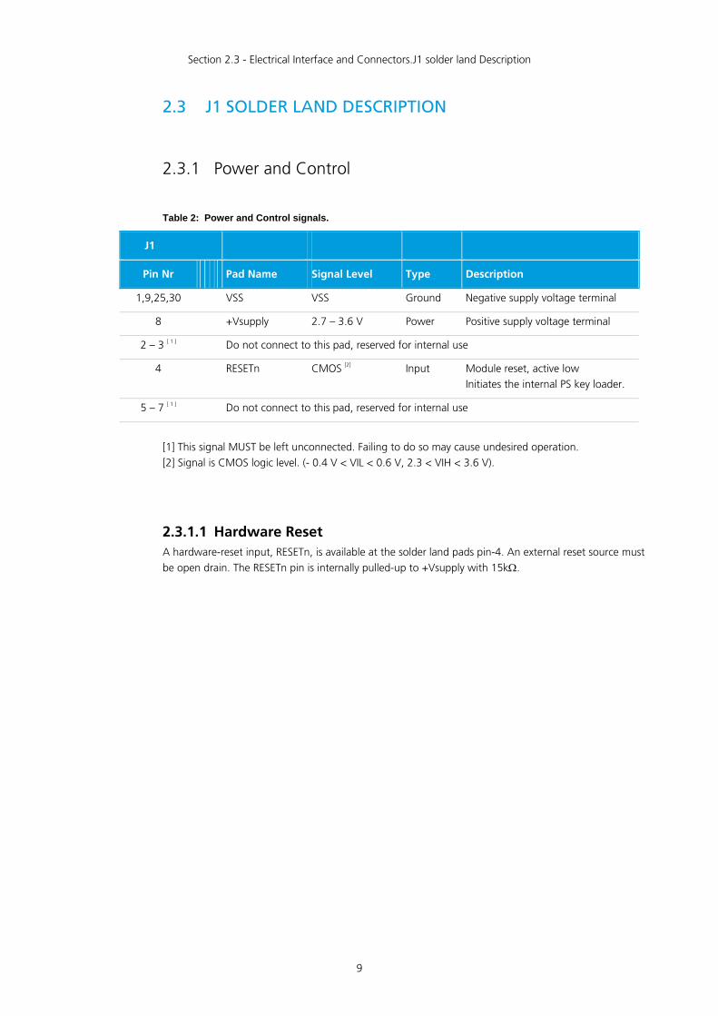
2.3 J1 SOLDER LAND DESCRIPTION
2.3.1 Power and Control
Table 2: Power and Control signals.
J1
Pin Nr Pad Name Signal Level Type Description
1,9,25,30 VSS VSS Ground Negative supply voltage terminal
8 +Vsupply 2.7 – 3.6 V Power Positive supply voltage terminal
2 – 3 [ 1 ] Do not connect to this pad, reserved for internal use
4
RESETn CMOS [2] Input Module reset, active low
Initiates the internal PS key loader.
5 – 7 [ 1 ] Do not connect to this pad, reserved for internal use
[1] This signal MUST be left unconnected. Failing to do so may cause undesired operation. [2] Signal is CMOS logic level. (- 0.4 V < VIL < 0.6 V, 2.3 < VIH < 3.6 V).
2.3.1.1 Hardware Reset A hardware-reset input, RESETn, is available at the solder land pads pin-4. An external reset source must be open drain. The RESETn pin is internally pulled-up to +Vsupply with 15kΩ.
Section 2.3 - Electrical Interface and Connectors.J1 solder land Description
10
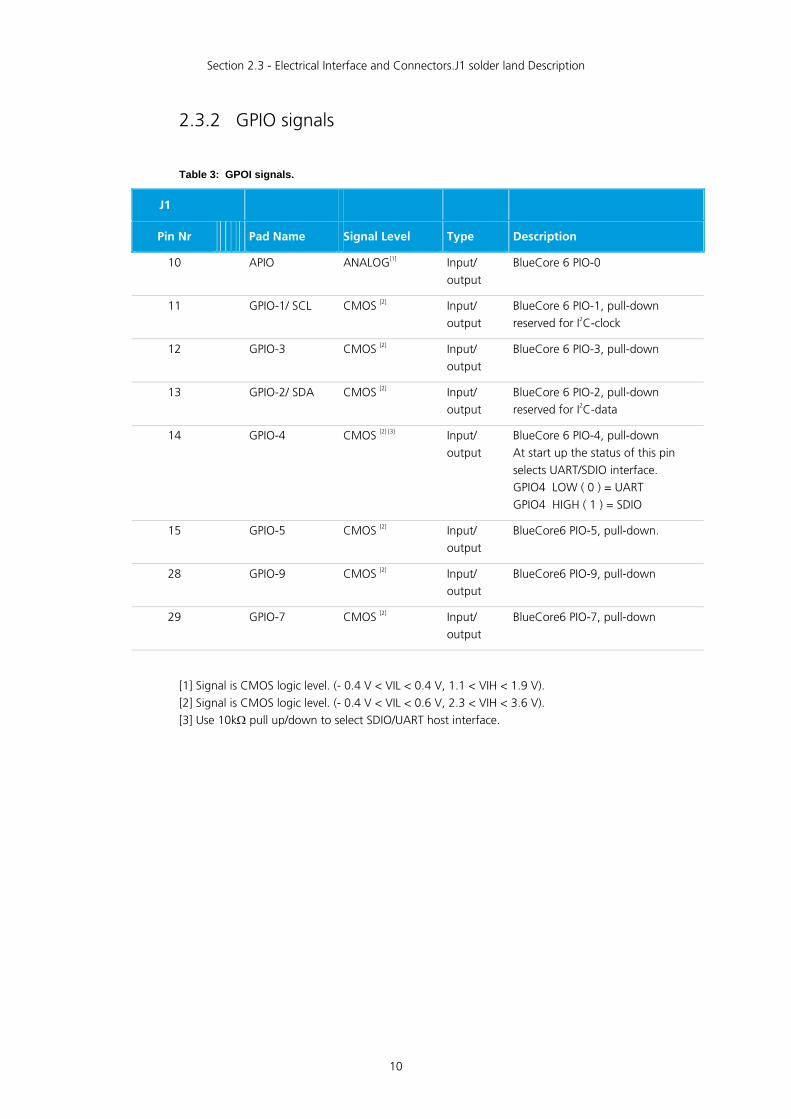
2.3.2 GPIO signals
Table 3: GPOI signals.
J1
Pin Nr Pad Name Signal Level Type Description
10 APIO ANALOG[1] Input/ output
BlueCore 6 PIO-0
11 GPIO-1/ SCL CMOS [2] Input/ output
BlueCore 6 PIO-1, pull-down reserved for I2C-clock
12 GPIO-3 CMOS [2] Input/ output
BlueCore 6 PIO-3, pull-down
13 GPIO-2/ SDA CMOS [2] Input/ output
BlueCore 6 PIO-2, pull-down reserved for I2C-data
14 GPIO-4 CMOS [2] [3] Input/ output
BlueCore 6 PIO-4, pull-down At start up the status of this pin selects UART/SDIO interface. GPIO4 LOW ( 0 ) = UART GPIO4 HIGH ( 1 ) = SDIO
15 GPIO-5 CMOS [2] Input/ output
BlueCore6 PIO-5, pull-down.
28 GPIO-9 CMOS [2] Input/ output
BlueCore6 PIO-9, pull-down
29 GPIO-7 CMOS [2] Input/ output
BlueCore6 PIO-7, pull-down
[1] Signal is CMOS logic level. (- 0.4 V < VIL < 0.4 V, 1.1 < VIH < 1.9 V). [2] Signal is CMOS logic level. (- 0.4 V < VIL < 0.6 V, 2.3 < VIH < 3.6 V). [3] Use 10kΩ pull up/down to select SDIO/UART host interface.

Section 2.3 - Electrical Interface and Connectors.J1 solder land Description
11
2.3.3 Host interface
Table 4: Host interface signals.
J1
Pin Nr Pad Name Signal Level Type Description
SDIO-CLK Input SDIO clock
CSPI-CLK Input CSPI clock
16
-
CMOS [2] weak pull-up
- -
SDIO-CSn Input SDIO chip select, active low
- - -
17
-
CMOS [2]
- -
SDIO-CMD Input SDIO data
CSPI-MOSI Input CSPI slave data input
18
-
CMOS [2] weak pull-up
- -
SDIO-DATA-3 In/Out Synchronous data I/O
CSPI-CSn Input CSPI chip select, active low
23
UART-CTS
CMOS [2]
Input UART clear to send, active low
SDIO-DATA-2 In/Out Synchronous data I/O
- - -
24
UART-RxD
CMOS [2]
Input UART receive data, active high
SDIO-DATA-1 In/Out Synchronous data I/O
CSPI-INT Input CSPI data
26
UART-RTS
CMOS [2]
Output UART request to send, active low
SDIO-DATA-0 In/Out Synchronous data I/O
CSPI-MISO Output CSPI slave data output
27
UART-TxD
CMOS [2]
Output UART transmit data, active high
[2] Signal is CMOS logic level. (- 0.4 V < VIL < 0.6 V, 2.3 < VIH < 3.6 V).

Section 2.3 - Electrical Interface and Connectors.J1 solder land Description
12
2.3.3.1 UART host interface selection During start up the status of pin 16 and 18 selects which type of UART interface to be used.
The UART supports standard baud rates between 9.6 k baud and 2764.8 k baud. The module auto negotiates the baud rate but It is recommended that for baud rates above 115.2 k the UART speed is set by writing to PSKEY “UART_BAUDRATE”.
The default settings for the UART are 8 data bits, 1 Stop bit, parity and flow control depends on selected protocol.
Table 5: UART host interface selection
J1 Pin Nr: 16 [SDIO-CLK]
Pin Nr: 18 [SDIO-CMD]
UART protocol
LOW (0) LOW (0) BCSP, Even Parity, No Flow control
LOW (0) High (1) H4, No Parity, HW Flow control
High (1) LOW (0) H4DS, No Parity, HW Flow control
High (1) High (1) H5, Even Parity No Flow control
Use 10kΩ pull up/down to select UART protocol
2.3.4 Audio Interface
Table 6: Audio interface signals.
J1
Pin Nr Pad Name Signal Level Type Description
PCM-SYNC In/Out Synchronous data sync, Bi-directional weak pull-down
19
I2S-WS
CMOS [2]
In/Out Synchronous data sync, Bi-directional weak pull-down
PCM-CLK In/Out Synchronous data clock, Bi-directional weak pull-down
20
I2S-SCK
CMOS [2]
In/Out Synchronous data clock, Bi-directional weak pull-down
PCM-OUT Output Synchronous data output tri-state,
weak pull-down 21
I2S-SD-OUT
CMOS [2]
Output Synchronous data output tri-state, weak pull-down
PCM-IN Input Synchronous data input, weak pull-down
22
I2S-SD-IN
CMOS [2]
Input Synchronous data input, weak pull-down
[2] Signal is CMOS logic level. (- 0.4 V < VIL < 0.6 V, 2.3 < VIH < 3.6 V).

Section 2.4 - Electrical Interface and Connectors.Characteristics
13
2.4 CHARACTERISTICS The cB-OHCI406 module has two linear voltage regulators, a 1.8 V regulator and a 1.5 V regulator.
The voltage level at the I/O-pins is the same as the supply voltage.
2.4.1 Power supply NOTE: Read the safety notes in chapter 7 before using the modules.
Table 7: Power supply
Symbol Parameter Value Unit
Min 2.7 VDC VDD Power supply
Max 3.6 VDC
Table 8: Current consumption
Symbol Mode Value Unit
Average 5 mA Not connected Idle
Average 35 mA Transmitting DH1
Peak 60 mA
Average 48 mA Transmitting DH5
Peak 60 mA
Average 50 mA
IDD @ VDD = 3.3V
Connected
Transmitting 3xEDR-DH5
Peak 60 mA

Section 2.4 - Electrical Interface and Connectors.Characteristics
14
2.4.2 Input/Output signals
Table 9: Input/output signals
Symbol Parameter Value Unit
Min -0.3 V VIN Low Logic LOW level input voltage
Max 0.8 V
Min 2.0 V VIN High Logic HIGH level input voltage
Max 3.3 V
VOUT Low Logic LOW level output voltage Max 0.6 V
VOUT High Logic HIGH level output voltage Min 2.3 V
IGPIO Sink and source current Max 4 mA
CGPIO Input capacitance Typ 5 pF
2.4.3 RF specification
Table 10: RF information
Symbol Parameter Value Unit
Channels 79
Min 2402 MHz f Frequency range
Max 2480 MHz
Δf Channel separation Typ 1 MHz
PTX RF output power Max +6 dBm
Receive sensitive level (BER < 0.1 %) Typ -86 dBm
Receive input level Max -10 dBm

Section 2.4 - Electrical Interface and Connectors.Characteristics
15
2.4.4 Environmental
Table 11: Temperatures characteristics
Parameter Product Variant Value Unit
Min cB-OHCI406i-04 -40 °C Storage temperature
Max cB-OHCI406i-04 +85 °C
Min cB-OHCI406i-04 [ 1 ] -30 °C Maximum operating temperature
Max cB-OHCI406i-04 +85 °C
[1] 8-DPSK EDR receiver sensitivity cannot be guaranteed below 0 °C.
2.4.5 Mechanical
Table 12: Mechanical characteristics
Parameter Product Variant Value Unit
Weight All 1.5 g

Section 3.1 - Antennas.Surface Mounted Antenna (Internal)
16
3 Antennas
3.1 SURFACE MOUNTED ANTENNA (INTERNAL)
Part Number cB-OHCI406i-04
Antenna name FR-S1-N-0-104
Manufacture Fractus
Gain 0 dBi
Antenna size (LxWxH)
7 x 3 x 1 mm
Comment The antenna gain is dependent of the mounting of the module. See section 4.2 for mounting the module considering the antenna.

Section 4.1 - Mounting Information.Board Outlines
17
4 Mounting Information
4.1 BOARD OUTLINES
Figure 4 cB-OHCI406 primary side dimensions [mm]
Figure 5 cB-OHCI406 profile dimensions [mm]

Section 4.1 - Mounting Information.Board Outlines
18
4.1.1 Solder land dimensions
Figure 6 cB-OHCI406 solder land dimensions [mm]

Section 4.2 - Mounting Information.Using the J6 PCB solder pads
19
4.2 USING THE J6 PCB SOLDER PADS
4.2.1 Host PCB In order to avoid short circuit to traces and vias on the module the host PCB footprint should not contain any traces or vias under the module except the pads interfacing the J1 pads. No other pads than the J1 should be soldered to the host PCB. For detailed information about the signals present on the solder lands see section 2.3
4.2.2 Mounting process • We strongly recommend the modules to be run through the solder process only once.
connectBlue devices will withstand up to two reflows at an absolute maximum temperature of 250°C.
• The PCB is made of FR4-type with Chemical Gold Pads.
• The modules are produced in a lead-free process with a lead-free soldering paste.
• It is recommended that the customers make their own electrical, climate, stress and vibration tests on the final assembled product to secure that the manufacturing process hasn't damaged or affected the Bluetooth module in any way.
• The modules are delivered on Tape and reel packed in drypack bags.
• The device recommended maximum reflow temperature is 245°C for 10 sec.
• The device absolute maximum reflow temperature is 250°C for 3 sec.
4.3 ANTENNA ISSUES The unit cannot be mounted arbitrary, because of the radio communication. The unit that has an internal surface mounted antenna cannot be mounted in a metal enclosure.
No metal casing or plastics using metal flakes should be used, avoid also metallic based paint or lacquer. Keep a minimum clearance of 5 mm between the antenna and the casing. Keep minimum 10 mm free space from metal around the antenna including under and above.
Section 5.1 - Bluetooth Information.General Information
20
5 Bluetooth Information
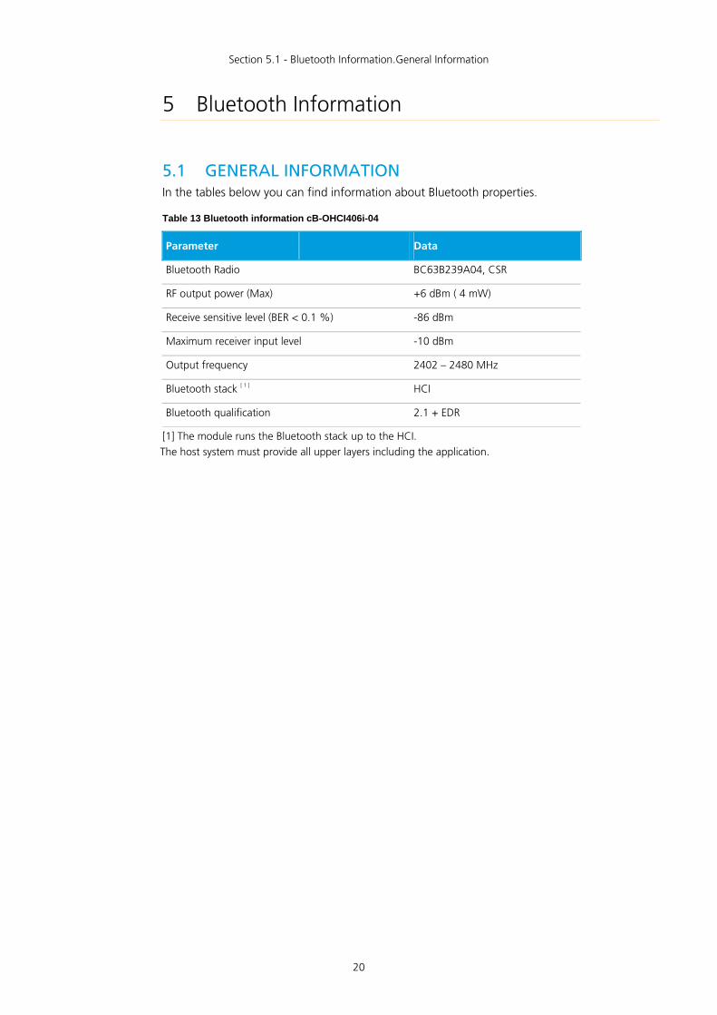
5.1 GENERAL INFORMATION In the tables below you can find information about Bluetooth properties.
Table 13 Bluetooth information cB-OHCI406i-04
Parameter Data
Bluetooth Radio BC63B239A04, CSR
RF output power (Max) +6 dBm ( 4 mW)
Receive sensitive level (BER < 0.1 %) -86 dBm
Maximum receiver input level -10 dBm
Output frequency 2402 – 2480 MHz
Bluetooth stack [ 1 ] HCI
Bluetooth qualification 2.1 + EDR
[1] The module runs the Bluetooth stack up to the HCI. The host system must provide all upper layers including the application.
Section 5.2 - Bluetooth Information.Bluetooth qualification information
21
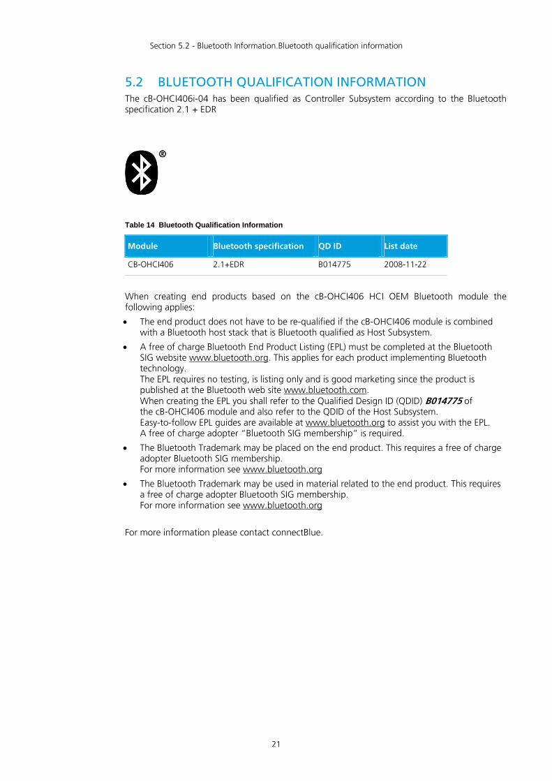
5.2 BLUETOOTH QUALIFICATION INFORMATION The cB-OHCI406i-04 has been qualified as Controller Subsystem according to the Bluetooth specification 2.1 + EDR
Table 14 Bluetooth Qualification Information
Module Bluetooth specification QD ID List date
CB-OHCI406 2.1+EDR B014775 2008-11-22
When creating end products based on the cB-OHCI406 HCI OEM Bluetooth module the following applies:
• The end product does not have to be re-qualified if the cB-OHCI406 module is combined with a Bluetooth host stack that is Bluetooth qualified as Host Subsystem.
• A free of charge Bluetooth End Product Listing (EPL) must be completed at the Bluetooth SIG website www.bluetooth.org. This applies for each product implementing Bluetooth technology. The EPL requires no testing, is listing only and is good marketing since the product is published at the Bluetooth web site www.bluetooth.com. When creating the EPL you shall refer to the Qualified Design ID (QDID) B014775 of the cB-OHCI406 module and also refer to the QDID of the Host Subsystem. Easy-to-follow EPL guides are available at www.bluetooth.org to assist you with the EPL. A free of charge adopter “Bluetooth SIG membership” is required.
• The Bluetooth Trademark may be placed on the end product. This requires a free of charge adopter Bluetooth SIG membership. For more information see www.bluetooth.org
• The Bluetooth Trademark may be used in material related to the end product. This requires a free of charge adopter Bluetooth SIG membership. For more information see www.bluetooth.org
For more information please contact connectBlue.

Section 6.1 - Regulatory Information.Declaration of Conformity
22
6 Regulatory Information
6.1 DECLARATION OF CONFORMITY
We, connectBlue AB, of Norra Vallgatan 64 3V SE-211 22 Malmö, Sweden
declare under our sole responsibility that our product:
cB-OHCI406i-04 (cB-0162-01) PCB no: cB-0921-02.
to which this declaration relates, conforms to the following product specifications:
R&TTE Directive 1999/5/EC:
Effective use of frequency spectrum:
EN 300 328 V1.7.1 (2006-05)
EMC:
EN 301 489-1 V1.4.1 (2002-08)
EN 301 489-17 V1.2.1 (2002-08)
EN 61000-6-2 (2001)
Health and safety:
EN 50371:2002
EN 60950-1:2001 and/or IEC 60950-1:2001 (1st Edition)
EN 60950-1/A11:2004 + Corrigendum:2004
Medical Electrical Equipment
IEC 60601-1-2 (2001)
26/10/2008 Malmö, Sweden
Mats Andersson
CTO of connectBlue AB
If a cB-OHCI406i-04 is used within EU a notification must be made to each of the national authorities responsible for radio spectrum management of the intention to place radio equipment that uses frequency bands whose use is not harmonized throughout the EU, on its national market. More information at: http://europa.eu.int/comm/enterprise/rtte/gener.htm

Section 6.2 - Regulatory Information.IC and FCC Compliance for cB-OHCI406i-04
23
6.2 IC AND FCC COMPLIANCE FOR CB-OHCI406I-04
6.2.1 IC Compliance Operation is subject to the following two conditions:
(1) this device may not cause harmful interference, and (2) this device must accept any interference received, including interference that may cause undesired operation.
This device is a modular transmitter with an on board antennas
The installer of this radio equipment must ensure that the antenna is located or pointed such that it does not emit RF field in excess of Health Canada limits for the general population; consult Safety Code 6, obtainable from Health Canada’s website www.hc-sc.gc.ca/rpb.
6.2.2 FCC Statement for cB-OHCI406i-04 This device complies with Part 15 of the FCC Rules. Operation is subject to the following two conditions: (1) this device may not cause harmful interference, and (2) this device must accept any interference received, including interference that may cause undesired operation.
NOTE: This equipment has been tested and found to comply with the limits for a Class B digital device, pursuant to Part 15 of the FCC Rules. These limits are designed to provide reasonable protection against harmful interference in a residential installation. This equipment generates, uses and can radiate radio frequency energy and, if not installed and used in accordance with the instructions, may cause harmful interference to radio communications. However, there is no guarantee that interference will not occur in a particular installation. If this equipment does cause harmful interference to radio or television reception, which can be determined by turning the equipment off and on, the user is encouraged to try to correct the interference by one or more of the following measures:
• Reorient or relocate the receiving antenna
• Increase the separation between the equipment and receiver
• Connect the equipment into an outlet on a circuit different from that to which the receiver is connected
Consult the dealer or an experienced radio/TV technician for help
6.2.3 Antenna Our module cB-OHCI406i-04 is for OEM integrations only. In the end-user product the module shall be professionally installed in such a manner that only the authorized antennas can be used.

Section 6.2 - Regulatory Information.IC and FCC Compliance for cB-OHCI406i-04
24
6.2.4 Caution Changes or modifications NOT expressly APPROVED by the party responsible for compliance could void the user‘s authority to operate the equipment.
6.2.5 Labeling Requirements for End Product For an end product using the product cB-OHCI406i-04 there MUST be a label containing, at least, the following information:
This device contains FCC ID: PVH092102 IC: 5325A-092102
The label must be affixed on an exterior surface of the end product such that it will be visible upon inspection in compliance with the modular approval guidelines developed by the FCC.
In accordance with 47 CFR § 15.19 the end product shall bear the following statement in a conspicuous location on the device:
“This device complies with Part 15 of the FCC Rules.
Operation is subject to the following two conditions:
(1) this device may not cause harmful interference, and (2) this device must accept any interference received, including interference that may cause undesired operation.”
When the device is so small or for such use that it is not practicable to place the statement above on it, the information shall be placed in a prominent location in the instruction manual or pamphlet supplied to the user or, alternatively, shall be placed on the container in which the device is marketed. However, the FCC ID label must be displayed on the device.
In case, where the final product will be installed in locations where the end-consumer is not able to see the FCC ID and/or this statement, the FCC ID and the statement shall also be included in the end-product manual.
6.2.6 RF-exposure Statement for cB-OHCI406i-04 This modular transmitter ultralow power device -fully complies with RF Exposure requirements.
Any notification to the end user of installation or removal instructions about the integrated radio module is NOT allowed.

Section 6.3 - Regulatory Information.UL listing information
25
6.3 UL LISTING INFORMATION If a customer intends to UL list a product containing the cB-OHCI406i-04 module based on the PCB cB-0921-02 this information is useful:
The printed circuit board if produced according to the following specification:
• UL recognized ZPMV2 min. 130 °C flame class V-0 or better.
6.4 COMPLIANCE WITH ROHS DIRECTIVE
The cB-OHCI406i-04 module is produced according to the RoHS (Restriction of the use of certain Hazardous substances in electrical and electronic equipment) directive and complies with the directive.

Section 7.1 - Guidelines for Efficient and Safe Use.General
26
7 Guidelines for Efficient and Safe Use
7.1 GENERAL Read this information before using your OEM Serial Port Adapter.
Note: Changes or modifications to the product not expressly approved by connectBlue AB will void the user’s authority to operate the equipment.
7.2 PRODUCT CARE • Do not expose your product to liquid or moisture.
• Do not expose you product to extreme hot or cold temperature (see Section 2.4.4 for further information).
• Do not expose your product to lit candles, cigarettes, cigars, open flames, etc.
• Do not drop, throw or try to bend your product since rough treatment could damage your product.
• Do not attempt to disassemble your product. Doing so will void warranty. The product does not contain consumer serviceable or replaceable components. Service should only be performed by connectBlue AB.
• Do not paint your product as the paint could prevent normal use.
• If you will not be using your product for a while, store it in a place that is dry, free from damp, dust and extreme heat and cold.
• The clearance and creepage distances required by the end product must be withheld when the module is installed.
• The cooling of the end product shall not negatively be influenced by the installation of the module when the module is installed.
7.3 RADIO FREQUENCY EXPOSURE The HCI Bluetooth module cB-OHCI406i-04 contains a small radio transmitter and receiver. During communication with other Bluetooth products the device receives and transmits radio frequency (RF) electromagnetic fields (microwaves) in the frequency range 2402 to 2480 MHz. The output power of the radio transmitter is very low.
When using the OEM HCI Bluetooth module cB-OHCI406i-04, you will be exposed to some of the transmitted RF energy. This exposure is well below the prescribed limits in all national and international RF safety standards and regulations.

Section 7.4 - Guidelines for Efficient and Safe Use.Electronic Equipment
27
7.4 ELECTRONIC EQUIPMENT Most modern electronic equipment, for example, in hospitals and cars, is shielded from RF energy. However, certain electronic equipment is not. Therefore:
Note: This equipment emits RF energy in the ISM (Industrial, Scientific, Medical) band. Please insure that all medical devices used in proximity to this device meet appropriate susceptibility specifications for this type of RF energy.
7.5 POTENTIALLY EXPLOSIVE ATMOSPHERES Turn off your electronic device before entering an area with potentially explosive atmosphere. It is rare, but your electronic device could generate sparks. Sparks in such areas could cause an explosion or fire resulting in bodily injury or even death.
Areas with a potentially explosive atmosphere are often, but not always, clearly marked. They include fuelling areas, such as petrol station, below deck on boats, fuel or chemical transfer or storage facilities, and areas where the air contains chemicals or particles, such as grain, dust, or metal powders.
7.6 SAFETY COMPLIANCE In order to fulfill the safety standard EN 60950-1:2001 the cB-OHCI406i-04 must be supplied by a class-2 Limited Power Source.
7.6.1 Power Supply • Connect your power supply only to designated power-sources as marked on the product.
• Make sure all cords and cable are positioned so that they will not be stepped on, tripped over or otherwise subject to damage or stress.
• To reduce risk of electric shock, unplug the unit from any power source before attempting to clean it.