bl1600 - digi internationalftp1.digi.com/support/documentation/0190016g.pdf · installation...
TRANSCRIPT

BL1600C-Programmable Controller
Users Manual001115 - G

BL1600 Users ManualPart Number 019-0016
001115 - G Printed in U.S.A.
Copyright© 1999 Z-World, Inc.
All rights reserved.
Z-World reserves the right to make changes and improvements to itsproducts without providing notice.
Trademarks Dynamic C
® is a registered trademark of Z-World, Inc.
Windows®
is a registered trademark of Microsoft Corporation
PLCBus
is a trademark of Z-World, Inc.
Hayes Smart Modem®
is a registered trademark of Hayes Microcom-puter Products, Inc.
Notice to UsersWhen a system failure may cause serious consequences, protecting life andproperty against such consequences with a backup system or safety deviceis essential. The buyer agrees that protection against consequencesresulting from system failure is the buyers responsibility.
This device is not approved for life-support or medical systems.
All Z-World products are 100 percent functionally tested. Additionaltesting may include visual quality control inspections or mechanicaldefects analyzer inspections. Specifications are based on characterizationof tested sample units rather than testing over temperature and voltage ofeach unit. Z-World may qualify components to operate within a range ofparameters that is different from the manufacturers recommended range.This strategy is believed to be more economical and effective. Additionaltesting or burn-in of an individual unit is available by special arrangement.
Company Address
Z-World, Inc.2900 Spafford StreetDavis, California 95616-6800USA
Telephone:Facsimile:Web Site:
E-Mail:
(530) 757-3737(530) 753-5141http://www.z w [email protected]

Table of Contents s iiiBL1600
TABLE OF CONTENTS
About This Manual vii
Chapter 1: Overview 11Introduction .......................................................................................... 12Features ................................................................................................ 13
Options and Upgrades ..................................................................... 14Development and Evaluation Tools ..................................................... 15
Software .......................................................................................... 15CE Compliance .................................................................................... 16
Chapter 2: Getting Started 17Initial BL1600 Setup ............................................................................ 18
Parts Required ................................................................................. 18Connecting the BL1600 to a Host PC .................................................. 18Running Dynamic C ............................................................................. 21
Chapter 3: BL1600 Operation 23Operating Modes.................................................................................. 24
Run Mode........................................................................................ 25EPROM................................................................................................ 25
Programming EPROMs .................................................................. 25Memory Size ................................................................................... 25Copyrights ....................................................................................... 27
Chapter 4: System Development 29BL1600 Interfaces ............................................................................... 30
Digital Inputs ................................................................................... 30Digital Outputs ................................................................................ 30Serial Ports ...................................................................................... 32Miscellaneous Signals ..................................................................... 33PLCBus Port ................................................................................... 34
Dynamic C Libraries ............................................................................ 35

iv s Table of Contents BL1600
Driver Software .................................................................................... 36Digital Inputs ................................................................................... 36Digital Outputs ................................................................................ 36High-Speed DMA Counter .............................................................. 37Battery-Backed Clock ..................................................................... 38Writing to Flash EPROM ................................................................ 38Virtual Drivers ................................................................................. 39
Invoking the Virtual Driver ........................................................... 41Virtual Driver Variables ................................................................ 41
Digital Inputs .............................................................................. 41Digital Outputs ........................................................................... 41Timers ......................................................................................... 42
Serial Communication .......................................................................... 43RS-232 Communication .................................................................. 43
Receive and Transmit Buffers ....................................................... 43Echo Option .................................................................................. 43CTS/RTS Control ......................................................................... 43XMODEM File Transfer .............................................................. 44Modem Communication ............................................................... 44
Software Support ............................................................................. 45Interrupt Handling for Z180 Port 0 ............................................... 45RS-232 Software Support ............................................................. 46XMODEM Commands ................................................................. 48Miscellaneous Functions .............................................................. 49
Master-Slave Networking ............................................................... 51RS-485 Network Hardware Connections ..................................... 52RS-485 Network Software Support .............................................. 54Miscellaneous RS-485 Network Functions .................................. 55
Support Libraries and Sample Programs......................................... 56Direct Programming of the Serial Ports ............................................... 57
Attainable Baud Rates ..................................................................... 57Z180 Serial Ports ............................................................................ 58
Asynchronous Serial Communication Interface (ASCI) ...................... 60ASCI Status Registers ..................................................................... 60
CTS1E (CTS Enable, Channel 1) ................................................. 61RDRF (Receiver Data Register Full) ............................................ 61
ASCI Control Register A ................................................................ 62ASCI Control Register B ................................................................ 63
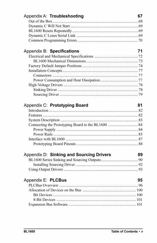
Table of Contents s vBL1600
Appendix A: Troubleshooting 67Out of the Box ...................................................................................... 68Dynamic C Will Not Start .................................................................... 69BL1600 Resets Repeatedly .................................................................. 69Dynamic C Loses Serial Link .............................................................. 69Common Programming Errors ............................................................. 70
Appendix B: Specifications 71Electrical and Mechanical Specifications ............................................ 72
BL1600 Mechanical Dimensions .................................................... 73Factory Default Jumper Positions ........................................................ 74Installation Concepts ............................................................................ 77
Connectors ...................................................................................... 77Power Consumption and Heat Dissipation ...................................... 77
High-Voltage Drivers ........................................................................... 78Sinking Driver ................................................................................. 78Sourcing Driver ............................................................................... 79
Appendix C: Prototyping Board 81Introduction .......................................................................................... 82Features ................................................................................................ 82System Description .............................................................................. 83Connecting the Prototyping Board to the BL1600 .............................. 84
Power Supply .................................................................................. 84Power Rails ..................................................................................... 85
Interface with BL1600 ......................................................................... 87Prototyping Board Pinouts .............................................................. 88
Appendix D: Sinking and Sourcing Drivers 89BL1600 Series Sinking and Sourcing Outputs ..................................... 90
Installing Sourcing Driver ............................................................... 92Using Output Drivers ........................................................................... 93
Appendix E: PLCBus 95PLCBus Overview ............................................................................... 96Allocation of Devices on the Bus ...................................................... 100
Bit Devices .................................................................................... 1008-Bit Devices ................................................................................ 101
Expansion Bus Software .................................................................... 101

vi s Table of Contents BL1600
Appendix F: EEPROM 107EEPROM Parameters ........................................................................ 108
Baud Rate ...................................................................................... 108Startup Mode ................................................................................. 108Clock Speed .................................................................................. 109
Changing Parameters Stored in EEPROM ......................................... 109Library Routines ................................................................................ 109
Appendix G: Memory, I/O Map, and Interrupt Vectors 111BL1600 Memory ................................................................................ 112
Memory and Input/Output Cycle Timing ...................................... 113Input/Output Cycle Timing ......................................................... 114
Execution Timing .......................................................................... 115Memory Map ..................................................................................... 116
Input/Output Select Map ............................................................... 116Z180 Internal Input/Output Registers Addresses 0x000x3F ....... 116Epson 72421 Timer Registers 0x40000x400F ............................ 118Other Addresses ............................................................................ 119
Interrupt Vectors ................................................................................ 121Nonmaskable Interrupts ................................................................ 122
Power Failure Interrupts ............................................................. 122Jump Vectors ................................................................................. 123Interrupt Priorities ......................................................................... 124
Appendix H: Power Management 125ADM691 Power Supervisor ............................................................... 126Power Failure Management ............................................................... 127
Power Failure Sequence ................................................................ 127Holdup Time ................................................................................. 129Multiple Power-Line Insults .......................................................... 129Sample Program to Handle Power Failure .................................... 130
Appendix I: Battery 131Battery Life and Storage Conditions .................................................. 132Replacing Soldered Lithium Battery .................................................. 132Battery Cautions ................................................................................ 133
Index 135
Schematics

BL1600 About This Manual s vii
ABOUT THIS MANUAL
This manual provides instructions for installing, testing, configuring, andinterconnecting the Z-World BL1600 controller. Instructions are alsoprovided for using Dynamic C® functions.
AssumptionsAssumptions are made regarding the user's knowledge and experience inthe following areas.
Ability to design and engineer the target system that the BL1600 willcontrol.
Understanding of the basics of operating a software program andediting files under Windows on a PC.
Knowledge of the basics of C programming.
For a full treatment of C, refer to the following texts.
The C Programming Language by Kernighan and Ritchie
and/or
C: A Reference Manual by Harbison and Steel
Knowledge of basic assembly language and architecture for the Z180microprocessor.
For documentation from Zilog, refer to the following texts.
Z180 MPU User's ManualZ180 Serial Communication ControllersZ80 Microprocessor Family User's Manual
$
$

BL1600viii s About This Manual
Table 1. Acronyms
Acronym Meaning
EPROM Erasable Programmable Read-Only Memory
EEPROM Electronically Erasable Programmable Read-Only Memory
NMI Nonmaskable Interrupt
PIO Parallel Input/Output Circuit(Individually Programmable Input/Output)
PRT Programmable Reload Timer
RAM Random Access Memory
RTC Real-Time Clock
SIB Serial Interface Board
SRAM Static Random Access Memory
UART Universal Asynchronous Receiver Transmitter
Terms and AbbreviationsTable 1 lists and defines the acronyms that may be used in this manual.
ConventionsTable 2 lists and defines the typographical conventions that may be used inthis manual.
Table 2. Typographical Conventions
Example Description
while Courier font (bold) indicates a program, a fragment of aprogram, or a Dynamic C keyword or phrase.
// IN-01… Program comments are written in Courier font, plain face.
Italics Indicates that something should be typed instead of theitalicized words (e.g., in place of filename, type a file’sname).
Edit Sans serif font (bold) signifies a menu or menu selection.
. . . An ellipsis indicates that (1) irrelevant program text isomitted for brevity or that (2) preceding program text maybe repeated indefinitely.
[ ] Brackets in a C function’s definition or program segmentindicate that the enclosed directive is optional.
< > Angle brackets occasionally enclose classes of terms.
a | b | c A vertical bar indicates that a choice should be made fromamong the items listed.

BL1600 About This Manual s ix
Pin Number 1
A black square indicatespin 1 of all headers.
Measurements
All diagram and graphic measurements are in inches followed by millime-ters enclosed in parenthesis.
IconsTable 3 displays and defines icons that may be used in this manual.
J1Pin 1
Table 3. Icons
Icon Meaning
$ Refer to or see
( Please contact
Caution
! Note
High Voltage
7,3 Tip
Factory Default
FD

BL1600x s About This Manual
Blank

BL1600 Overview s 1-11
CHAPTER 1:
OVERVIEW
Chapter 1 provides an overview and a brief description of the BL1600features.

BL160012 s Overview
IntroductionThe BL1600s combination of logic-level inputs/outputs and high-currentdrivers makes it a versatile controller in a compact form factor. TheBL1600 is ideal for OEM applications such as industrial control and dataacquisition.
The BL1600s battery-backed RAM, real-time clock, and EEPROMprovide data integrity in the event of power fluctuations or power failure.The BL1600 is readily connected to peripheral devices through standardheaders or screw terminals. An optional Prototyping Board facilitates thedevelopment of custom circuits and operator interfaces.
Figure 1-1 illustrates the BL1600 board layout.
Y1
Z180
H5
H4
U1 U2
U6
U11
U7 U8
U12
U13
U3
U4
U16
U17 U18J3
U9 U10
U14
H1 H2 H3
J1
J2
MV1
MV2
D1
Z1
C8
C16
EPROM RAM
RTC
EEPROM
PAL
U15
PLC
Bus
Por
t
Sup
er.
H.V
. Driv
er
Inputs 011 Misc. Outputs
U5
Reg.
K
GND
Mis
c.
Battery
RS-232
RS-232
RS-485
HI7
HI6
HI5
HI4
HI3
HI2
HI1
RS485+
RS485
DCIN
Figure 1-1. BL1600 Board Layout
BL1600 Overview s 1-13
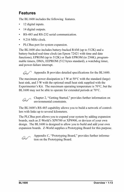
FeaturesThe BL1600 includes the following features.
12 digital inputs.
14 digital outputs.
RS-485 and RS-232 serial communication.
9.216 MHz clock.
PLCBus port for system expansion.
The BL1600 also includes battery-backed RAM (up to 512K) and abattery-backed real-time clock (an Epson 72421 with time and datefunctions), EPROM (up to 512K) or flash EPROM (to 256K), program-mable timers, DMA, EEPROM (512 bytes standard), a watchdog timer,and power-failure interrupt.
Appendix B provides detailed specifications for the BL1600.
The maximum power dissipation is 5 W at 50°C with the standard (large)heat sink, and 3 W with the optional small heat sink supplied with theExperimenters Kit. The maximum operating temperature is 70°C, but theBL1600 may not be able to operate for extended periods at 70°C.
Chapter 2, Getting Started, provides further information onenvironmental constraints.
The BL1600s RS-485 capability allows you to build a network of control-lers with links up to several kilometers.
The PLCBus port allows you to expand your system by adding expansionboards, such as Z-Worlds XP8700 or XP8900, or devices of your owndesign. The BL1600 is designed to allow you to build and add your ownexpansion boards. Z-World supplies a Prototyping Board for this purpose.
Appendix C, Prototyping Board, provides further informa-tion on the Prototyping Board.
$
$
$

BL160014 s Overview
(
Options and Upgrades
The BL1600 Series of controllers has two versions. Table 1-1 lists theirstandard features.
The following optional items are available for BL1600 Series controllers.
128K or 256K flash EPROM to replace regular EPROM.
128K or 512K SRAM.
Prototyping Board.
XP8700 expansion board to program the BL1600 if the BL1600sRS-232 serial port is required by the application. A full line ofZ-World expansion boards is available.
For ordering information, call your Z-World Sales Representa-tive at (530) 757-3737.
Table 1-1. BL1600 Series Features
Model Features
BL1600 9.216 MHz clock, 12 digital inputs, 14 high-currentsinking outputs, RS-232/RS-485 serial ports, EEPROM,real-time clock, PLCBus expansion port.
BL1610 BL1600 without serial ports, high-current drivers,EEPROM, or real-time clock.

BL1600 Overview s 1-15
Development and Evaluation ToolsThe BL1600 is supported by a Developers Kit that include everything youneed to start development with the BLl600.
The Developers Kit includes these items.
Programming cables and adapter.
24 V DC wall-mount power supply.
128K flash EPROM.
Smaller heat sink.
Sinking and sourcing high-current driver chips.
14-pin and 20-pin breakout cables.
Software
The BL1600 is programmed using Z-Worlds Dynamic C, an integrateddevelopment environment that includes an editor, a C compiler, and adebugger. Library functions provide an easy and robust interface to theBL1600.
Z-Worlds Dynamic C reference manuals provide completesoftware descriptions and programming instructions.$

BL160016 s Overview
$
CE ComplianceThe BL1600 has been tested by an approved competentbody, and was found to be in conformity with applicableEN and equivalent standards. Note the following require-ments for incorporating the BL1600 in your application tocomply with CE requirements.
The power supply provided with the Development Kit if for develop-ment purposes only. It is the customers responsibility to provide aclean DC supply to the controller for all applications in end-products.
The BL1600 has been tested to Light Industrial Immunity standards.Additional shielding or filtering may be required for an industrialenvironment.
The BL1600 has been tested to EN55022 Class A emission standards.Additional shielding or filtering may be required to meet Class Bemission standards.
Visit the Technical Reference pages of the Z-World Web siteat http://www.zworld.com for more information on shieldingand filtering.

BL1600 Getting Started s 17
CHAPTER 2:
GETTING STARTED
Chapter 2 provides instructions for connecting the BL1600 to a host PCand running a sample program.

BL160018 s Getting Started
Initial BL1600 Setup
Parts Required
24 V unregulated DC power supply
Programming cable
Optional XP8700 expansion board (needed if the RS-232 port on theBL1600 is required by the application).
The necessary parts are supplied with the Developers Kit.
Connecting the BL1600 to a Host PC1. Connect the power supply to the BL1600. Connect the two leads from
the DC power supply or wall transformer to header J2 as shown inFigure 2-1. Do not power up the power supply until the remainingsteps have been completed.
Figure 2-1. Bl1600 Power Supply Connections at Header J2
Be careful to connect the power supply wires to the correctsockets on header H2. The BL1600 may be destroyed in aninstant if the power supply is connected to the wrong socket.A protective diode prevents damage to the BL1600 if thepower supply polarity is reversed.
DCIN
J2
K
HC7
HC6
HC5
HC4
HC3
HC2
HC1
RS485+
RS485
GND to walltransformer

BL1600 Getting Started s 19
2. Check jumper settings on header J1. Jumpers on header J1 define thehardware configuration, the mode, and the baud rate. Figure 2-2 showsthe jumper settings for the various programming options.
Figure 2-2. BL1600 Programming Jumper Settings for Header J1
Appendix B, Specifications, lists all the jumper settings.
3. Establish a serial communication link. A PC communicates with theBL1600 via Serial Port 0 on the BL1600s microprocessor using RS-232protocols. There are two options to install the communication link.
Option 1BL1600 serial port (header H3).
Use the programming cable to connect the PCs 9-pin or 25-pin RS-232serial port to header H3 on the BL1600 as shown in Figure 2-3. EitherPC serial port (COM1 or COM2) may be used.
Figure 2-3. Connecting Programming Cable to BL1600 Header H3
H3
J2BL1600
to PCCOM port
9-pin to 25-pinadapter
(optional)
9-pin serialconnector
Walltransformer
$
Run program from RAM
J1
1
2
3
4
5
6
7
8
Program at 9600 bps
J1
1
2
3
4
5
6
7
8
J1
1
2
3
4
5
6
7
8
J1
1
2
3
4
5
6
7
8
Program at 19,200 bps
FD
Program at baud ratestored in EEPROM location 1

BL160020 s Getting Started
P1
J1
Latch
D2
P2
H1
U5
PAL
PAL
U6
U4
SCC2691 UART
U1
3.686MHz
U2
RN1
D1R2R1
C1 C3 C4 C2
H2
RS-232 DriverRS-232
Jack
XP8700
BL1600
H5
H4
U1 U2
U6
U11
J4
H1
Battery
serial cableto PC
H1
Option 2XP8700 expansion board.
Use the programming cable to connect the PCs 9-pin or 25-pin RS-232serial port to header H1 on the XP8700. Either PC serial port (COM1or COM2) may be used. (If you are using a non-Z-World programmingcable with an RJ-12 plug instead of a 10-pin connector, connect theRJ-12 plug to the RJ-12 jack on the XP8700.) Connect the XP8700 tothe BL1600s PLCBus port as shown in Figure 2-4.
Figure 2-4. Use of XP8700 to Program BL1600
4. The BL1600 is now ready for programming. The power supply may beplugged in and turned on.

BL1600 Getting Started s 21
!
Running Dynamic CDouble-click the Dynamic C icon to start the software. Note that the PCattempts to communicate with the BL1600 each time Dynamic C isstarted. No error messages are displayed once communication is estab-lished.
The communication rate, port, and protocol are all selected by choosingSerial Options from Dynamic Cs OPTIONS menu.
The BL1600s default communication rate is 19,200 bps. However, theDynamic C software shipped by Z-World may be initialized for a differentrate. To begin, adjust the communications rate to 19,200 bps.
Make sure that the PC serial port used to connect the serial cable (COM1or COM2) is the one selected in the Dynamic C OPTIONS menu. Selectthe 1-stop-bit protocol.
See Appendix A, Troubleshooting, if an error message suchas Target Not Responding or Communication Error appears.
Once the necessary changes have been made to establishcommunication between the host PC and the BL1600, use theDynamic C shortcut <Ctrl Y> to reset the controller and initiatecommunication.
$

BL160022 s Getting Started
Blank

BL1600 BL1600 Operation s 23
CHAPTER 3:
BL1600 OPERATION
Chapter 3 describes how to use the BL1600, with a focus on
how to set the run and programming modes, and
how to burn a custom program on EPROM.
BL160024 s BL1600 Operation
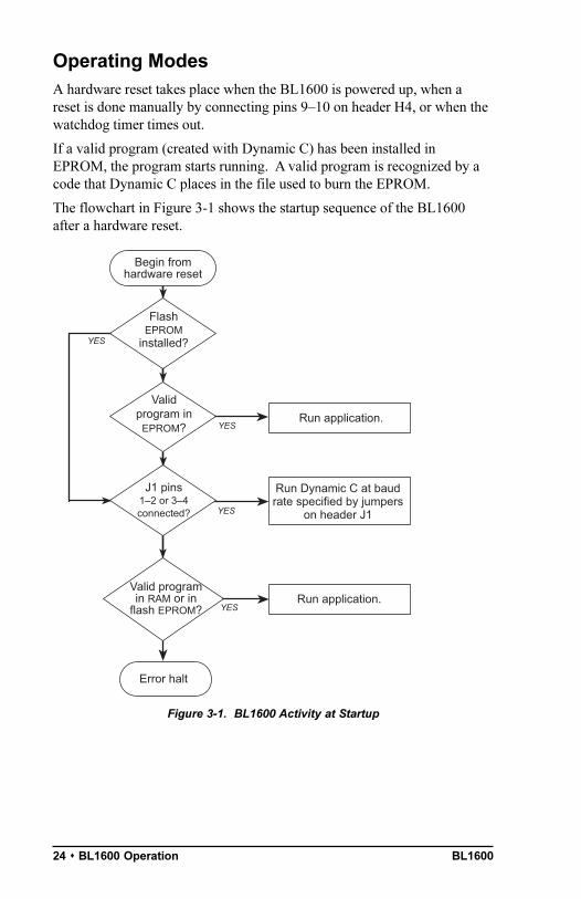
Operating ModesA hardware reset takes place when the BL1600 is powered up, when areset is done manually by connecting pins 910 on header H4, or when thewatchdog timer times out.
If a valid program (created with Dynamic C) has been installed inEPROM, the program starts running. A valid program is recognized by acode that Dynamic C places in the file used to burn the EPROM.
The flowchart in Figure 3-1 shows the startup sequence of the BL1600after a hardware reset.
Figure 3-1. BL1600 Activity at Startup
Begin fromhardware reset
YES
Run application.YES
Run Dynamic C at baudrate specified by jumpers
on header J1
J1 pins12 or 34connected?
YES
YES
Validprogram in
EPROM?
FlashEPROM
installed?
Valid programin RAM or in
flash EPROM?
Error halt
Run application.

BL1600 BL1600 Operation s 25
Run Mode
Before running a program from battery-backed RAM or flash EPROM, besure pins 12 and 34 on header J1 are not connected. If a valid userprogram is already in EPROM, that program will run immediately after ahardware reset.
If the Dynamic C EPROM is present on the board, the BL1600executes the program stored in battery-backed RAMthat is,the program last run under Dynamic C. If the Dynamic CEPROM has been replaced with a custom EPROM, then theBL1600 executes that program.
EPROM
Programming EPROMs
Dynamic C can be used to create a file for programming an EPROM byselecting the Compile to File option in the COMPILE menu. The BL1600must be connected to the PC running Dynamic C during this step becauseessential library routines must be uploaded from the Dynamic C EPROMand linked to the resulting file. The output is a binary file (optionally anIntel hex format file) that can be used to build an application EPROM.The application EPROM is then programmed with an EPROM program-mer that reads either a binary image or the Intel hex format file. Theresulting application EPROM can then replace the EPROM that came withthe BL1600.
Whenever the Dynamic C EPROM is replaced by a custom EPROM, theBL1600 ignores the program in battery-backed RAM in favor of theprogram stored in EPROM.
Memory Size
When doing program development with Dynamic C, it is best to use a128K SRAM or larger. Dynamic C will work with a 32K SRAM, but thetotal program space will be limited to 16K of root and 16K of extendedmemory. This is enough for many programs, but it is inconvenient to runout of memory during development. Once a program is burned intoEPROM, there is no reason to use SRAM larger than 32K unless the dataspace is larger than 32K.
!

BL160026 s BL1600 Operation
U8
28-pinSRAMEPROM
U7
EPROM
U7
U1U8
32-pinSRAM
J1 6-8-10
5-7-9
12-14-16
11-13-15
J1 6-8-10
5-7-9
12-14-16
11-13-15
FD
FD
FD
J1
6
5 7 9 11 13 15
8 10 12 14 16
non-Flash EPROM
J1
6
5 7 9 11 13 15
8 10 12 14 16
J1
6
5 7 9 11 13 15
8 10 12 14 16
Flash EPROM
32K EPROM
J1
6
5 7 9 11 13 15
8 10 12 14 16
64K, 128K EPROM
J1
6
5 7 9 11 13 15
8 10 12 14 16
J1
6
5 7 9 11 13 15
8 10 12 14 16
256K, 512K EPROM
32K, 128 K SRAM
J1
6
5 7 9 11 13 15
8 10 12 14 16
512K SRAM
The BL1600 can accommodate SRAM and EPROM chips from 32K to 512K,and flash EPROM from 64K to 256K. The memory chips may have 28 or 32pins, and must be seated in the sockets as shown in Figure 3-2. The locationof pin 1 relative to the socket varies, depending on the size of the chip.
Figure 3-2. Placement of 28-pin and 32-pin EPROMs on BL1600
The corresponding jumper settings for header J1 are shown in Figure 3-3.
Figure 3-3. BL1600 Jumper Settings for Different-Sized SRAM and EPROM
Either 28-pin or 32-pin chips may be used.

BL1600 BL1600 Operation s 27
Copyrights
The Dynamic C library is copyrighted. Place a label containing the follow-ing copyright notice on the EPROM whenever an EPROM that containsportions of the Dynamic C library is created.
©19911995 Z-World.
Your own copyright notice may also be included on the label to protectyour portion of the code.
Z-World grants purchasers of the Dynamic C software and the copyrightedEPROM library permission to copy portions of the EPROM library asdescribed above, provided that the following two conditions are compliedwith.
1. The resulting EPROM are used only with BL1600 controllersmanufactured by Z-World.
2. Z-Worlds copyright notice is placed on all copies of the EPROM.

BL160028 s BL1600 Operation
Blank

BL1600 System Development s 29
CHAPTER 4:
SYSTEM DEVELOPMENT
Chapter 4 provides the following information to develop the BL1600 forspecific uses.
BL1600 interfaces
Dynamic C libraries
Driver software
Serial communication
Direct programming of the serial ports
Asynchronous serial communication interface

BL160030 s System Development
BL1600 InterfacesFigure 4-1 shows a block diagram of the BL1600.
Figure 4-1. BL1600 Block Diagram
Digital Inputs
The 12 digital inputs, IN00IN11, ac-cept CMOS levels, which are at adigital threshold of approximately 2.5V. The digital inputs are arranged intwo groups, IN00IN07 and IN08IN11, on header H1. Each input linehas a 4.7 kΩ pull-up resistor. Figure4-2 shows the pinout for header H1.
Although the digital inputs are IN00-IN11, the softwarefunction calls refer to the channels as channels 112.
Digital Outputs
There are 14 digital outputs. The EN485 line can be used as an additionaldigital output if RS-485 communication is not usedno special jumpersettings or software calls have to be made. The SCL line can be used as anadditional digital output on the Bl1610, which has no EEPROM.
The output lines are arranged into two groups.
OUTB1OUTB8 eight 8-bit parallel outputs
OUT1OUT6, EN485 and SCL eight individually selectable lines
IN00IN02IN04IN06IN08IN10GND
135791113
2468
101214
H1 IN01IN03IN05IN07IN09IN11
+5 V
Figure 4-2. BL1600 Digital InputsHeader H1 Pinout
DigitalOutput
Z180
RAM
EPROM
EEPROM
Real-Time Clock
Battery
DigitalInput
User lines
E, Interrupt, ResetMisc.
OUTB
OUTSCL
PLCBus HC
KHigh-current output
+
3
2DMA request
3
8
7
7 7
12IN
OUT7 is the same as EN485.If you use EN485 to enableRS485 transmission, it is notavailable as an output.
Each user line selects agroup of 16 registers.
RS-485
RS-232
!

BL1600 System Development s 31
The OUTB1OUTB8 and SCL sig-nals are carried on header H2 asshown in Figure 4-3.
Seven of the digital outputs(OUT1OUT6 and EN485) feedthe high-current driver, providingseven high-current outputs (HC1HC7) suitable for driving relays, so-lenoids, or lamps. The high-currentoutputs are available on header J2as shown in Figure 4-4.
Figure 4-4. BL1600 Header J2 Pinout
Each high-current output includes a protective diode that can returninductive spikes to the power supply. The diodes use a common bus (K).Sinking drivers are the factory default. Sourcing drivers may also be used.Both can be seated in the same 18-pin socket.
See Appendix D, Sinking and Sourcing Drivers, for moreinformation on using or changing between sinking andsourcing driver chips.
OUTB7
OUT1OUT3OUT5
EN485
OUTB1OUTB3OUTB5
135791113151719
2468
101214161820
H2GND
OUTB8
OUT2OUT4OUT6SCLGNDOUTB2OUTB4OUTB6
+5 V
+5 V
Figure 4-3. BL1600 Digital OutputsHeader H2 Pinout
DCIN
K
HC7
HC6
HC5
HC4
HC3
HC2
HC1
RS485+
RS485
GND
High-currentoutputs
J2
$

BL160032 s System Development
13579
2468
10
H3/TX0 /RX1 or /CTS0
/RX0 /TX1 or /RTS0
J1
27
282624
23 2519
20
J1
27
282624
23 2519
20
21
22
21
22
FD
Two3-wire RS-232
One5-wire RS-232
& 2-wire RS-485
18
17
/CTS0
RXD1
TXD1
RXD0
TXD0
Z180 /RX1
/TX1
/RX0
/TX0
RS232CH1RX
RS232CH1TX
RXD0
TXD0
J1
20 22
24 23
/RTS0
485
485+
TXD1
RX485
J1 toH3
toJ2
U4(RS-232)
U9(RS-485)
Serial Ports
Two serial ports support asynchronous communication at baud rates from300 bps to 57,600 bps. The drivers can be configured either as two 3-wireRS-232 ports or as one 5-wire RS-232 port (with RTS and CTS) and onehalf-duplex RS-485 port.
Header H3 supports full-duplex RS-232 communication with handshakelines. The RS-485 lines (on the screw terminals, header J2) provide half-duplex asynchronous communication over twisted pair wires up to 3 km.
Figure 4-5 illustrates the pinout on header H3 for RS-232 communicationand provides the appropriate RS-232 and RS-485 jumper settings on head-er J1. Figure 4-4 shows the location of the RS-485 signals on header J2.
Figure 4-5. BL1600 RS-232 Serial PortHeader H3 Pinout and Jumper Settings
When header H3 is used as the programming port, it cannot beused as a communication port by the application. Refer toChapter 2, Getting Started, for information on how to pro-gram with an XP8700 expansion board if your application willneed header H3.
Figure 4-6 shows the configuration of two 3-wire RS-232 channels.
Figure 4-6. BL1600 Configuration for Two 3-wire RS-232 Channels
!

BL1600 System Development s 33
RX485
/CTS0
RXD1
TXD1
RXD0
TXD0
Z180 /CTS0
/RTS0
/RX0
/TX0
RS232CH1RX
RS232CH1TX
RXD0
TXD0
18 20/RTS0
485
485+
TXD1
J1 toH3
toJ2
25 23
24 26J1
U4(RS-232)
U9(RS-485)
13579
2468
10
H4/USER2 /DREQ0/USER3 /DREQ1
/USER1
E/RESET/INT2
Figure 4-8. BL1600 Miscellaneous SignalsHeader H4 Pinout
Figure 4-7 shows the configuration for one 5-wire RS-232 channel and one2-wire RS-485 channel.
Figure 4-7. BL1600 Configuration for One 5-wire RS-232 Channeland One 2-wire RS-485 Channel
The high-current output chip, U10, and the RS-485 driver, U9,are coupled, so that disabling the RS-485 driver will alsodisable the high-current output. The EN485 line may be usedas high-current output HC7 if RS-485 communication is notneeded.
Miscellaneous Signals
Header H4, shown in Figure 4-8,has three user lines, two DMArequest lines, and three miscel-laneous signals. These signalsare provided to support cus-tomer-designed expansionboards for the BL1600. The sig-nals are discussed briefly.
/USER1/USER3
Coupled with address lines A0A3, /USER1/USER3 allow you to readand write to as many as 48 devices (registers) in your system. Only oneline asserts at any one time. Each line identifies a group of registers. Thegroups have the following base addresses.
/USER1 0x150/USER2 0x160/USER3 0x170
A registers address is group + register#. For example, to read or write toregister 5 of group 2, use address 0x165.
!
BL160034 s System Development
/DREQ0, /DREQ1
These are DMA request lines for Z180 DMA Channels 0 and 1.
/INT2
This interrupt line is available to the designer. (/INT0 is reserved and /INT1is the PLCBus interrupt.)
/RESET
The /RESET signal can be used to manually reset the BL1600. A pushbut-ton reset switch may be added across pins 9 and 10 of H4.
E
The E signal is useful for customer-designed expansion boards for theBL1600.
Refer to page 39 of the Zilog Z180 MPU Users Manual formore information about using E.
PLCBus Port
Header H5 provides the PLCBus signals. The eight data lines on thisheader can be used as TTL-level inputs and outputs if the PLCBus is nototherwise used.
Refer to Appendix E, PLCBus, for more information aboutthe PLCBus.
$
$

BL1600 System Development s 35
Dynamic C LibrariesFunctions specific to the BL1600 can be found in the software librariessupplied with Dynamic C. These libraries are maintained in source codeso they can be easily modified or augmented by the user. The BL1600functions are in the BL16XX.LIB, CPLC.LIB, DRIVERS.LIB, AASC.LIB,and SERIAL.LIB libraries.
Whenever unresolved calls to functions remain after an application iscompiled, Dynamic C scans all the source libraries for functions with thatname. When found, the functions are extracted from the library and arecompiled with the application. The libraries are scanned until no moreunresolved names are found, so library functions can call other libraryfunctions and their order of appearance in the library is not important.
Dynamic C also accesses a library in the EPROM on the BL1600 board.This library is in machine language and the library functions can be calleddirectly from a program. This library has the advantage that the code doesnot need to be downloaded, reducing the compile time, particularly for thestandard version of Dynamic C with its slower communication rate. TheEPROM library version is used if the same function appears in both theEPROM library and the source library.
Use the following preprocessor command to replace a function in theEPROM library.
#KILL func1, func2, func3 . . .
This causes the specified functions in the EPROM library to be ignored.Replaceable functions in the EPROM library have a period (.) in theirname. The KILL directive will change the period to an underscore (_),causing a search for a legal C name to occur. Your own version of thefunction can then be added to the program or taken from one of thelibraries.
The Dynamic C SAMPLES\BL16XX subdirectory provides sample pro-grams to illustrate the software described in this chapter.

BL160036 s System Development
Driver SoftwareZ-Worlds drivers make it easy to communicate with the BL1600 inputs andoutputs. A direct driver immediately reads or writes to the controlled hardware.An indirect driver uses intermediate variables. Z-Worlds virtual driver(described later in this section under Virtual Drivers) is a periodically calledinterrupt service routine that connects the hardware with intermediate variables.
Low-level drivers return, send, or transmit values as received or as present-ed by the hardware interface. High-level drivers modify the inputs oroutputs in some way, such as by introducing calibration, hysteresis or aver-aging. Indirect, high-level drivers eliminate concerns about the technicaldetails of the I/O interface, but the price for this convenience is a slightloss of speed and efficiency.
Digital Inputs
int up_digin( int chan )
Gets the value at the specified digital input channel chan (112).
RETURN VALUE: 1 when the input voltage is high (>2.5 V) and 0when the input voltage is low.
Digital Outputs
There are 14 digital outputs, plus two additional outputs (EN485 and SCL)that depend on the hardware. Z-Worlds driver software library does notprovide drivers for the additional outputs. CPLC.LIB needs to be modi-fied to use EN485 and SCL as digital outputs.
Outputs 18 correspond to the signals OUTB1OUTB8. Outputs 914correspond to OUT1OUT6. Outputs 914 also feed the high-currentdriver (HC1HC6).
Bear in mind that the total number of high-current outputs that can be on atone time is subject to chip power limits and ambient temperature. With thesinking driver (ULN2003), no more than two 500 mA channels per chipshould be on continuously. All channels can be on at once as long as theydo not consume more than 100 mA per channel. The UDN2985A chipscan drive all channels at 30 V and 250 mA per channel at 25°C.
All 14 digital outputs appear on H2. A 0 makes the output on H2 low; a 1makes it high. For outputs 914, a 0 switches the high-current output offand a 1 turns it on. Sinking driver outputs pull low when turned on;sourcing driver outputs pull high.
int up_setout( int channel, int value )
Turns on a digital output. Pass channel number (114) and value (0for OFF, 1 for ON).
A 0 turns the output off, 1 turns the output on. Digital outputs 914support high-current channels 16.

BL1600 System Development s 37
High-Speed DMA Counter
The two DMA channels of the Z180 are used as high-speed counters (up to500 kHz). Function calls load the countdown value for the DMA channeland enable the DMA interrupt. Once a counter reaches zero, flags for theDMA channel are set to 1. Your program can monitor these flags.
void DMA0Count( unsigned integer count )
Loads DMA Channel 0 with the count value and enables the DMAChannel 0 interrupt. The function sets the flag _DMAFLAG0 to zero.When count negative edges have been detected, the channel will causean interrupt and the interrupt service routine will set the flag_DMAFLAG0 to 1. A program can monitor _DMAFLAG0 to determine ifthe number of counts has occurred.
void DMA1Count( unsigned integer count )
Loads DMA Channel 1 with the count value and enables the DMA Chan-nel 1 interrupt. The function sets the flag _DMAFLAG1 to zero. When countnegative edges have been detected, the channel will cause an interrupt andthe interrupt service routine will set the flag _DMAFLAG1 to 1. A programcan monitor _DMAFLAG1 to determine if the number of counts has occurred.
unsigned integer DMASnapShot( byte channel,unsigned integer *counter )
Reads the number of pulses that a DMA channel (0 or 1) has counted. ADMA counter is initialized with one of the two preceding functions. If aDMA channel is counting too fast to allow for stable reading of the countvalue, the function returns 0. If the function reads a stable count value, itreturns 1 and sets the parameter count. Note that even if you are unableto read the counts, DMA interrupts will still occur when the DMA channelcounts down from its loaded value.
Sample DMA Counter Program
main()unsigned integer count, oldcount;oldcount = 0;DMA0Count( 100 ); // count 100 pulseswhile( !DMA0FLAG ) // not finished
if( DMASnapShot(0,&count) ) // is it stable?if( oldcount != count )
oldcount = count;printf( DMA counted %u\n, count );
printf( finished counting\n );

BL160038 s System Development
GENDMA.C in the SAMPLES\BL16XX directory illustrates the use of DMAfunctions.
Battery-Backed Clock
The battery-backed clock retains the time and date with a resolution of onesecond, and an accuracy of about one second per day. It automaticallyaccounts for leap year.
The following structure is used to hold the time and date:
struct tm char tm_sec; // 0-59char tm_min; // 0-59char tm_hour; // 0-23char tm_mday; // 1-31char tm_mon; // 1-12char tm_year; // 0-150 (1900-2050)char tm_wday; // 0-6 where 0 means Sunday
;
The following routines are used to read and write the clock.
int tm_wr( struct tm *x ); // write the clock
int tm_rd( struct tm *x ); // read the clock
The following routines convert the time to and from a long integer. Thelong-integer format represents the number of seconds that have passedsince January 1, 1980 at midnight (00:00:00).
// return long seconds from structurelong mktime( struct tm *t );
// return structure from long secondsint mktm( struct tm *t, long time );
The long-integer format is convenient for comparing dates and times. Themktime function correctly handles dates beyond the year 2000.
Writing to Flash EPROM
int WriteFlash( unsigned long addr, char* buf,int num )
Writes num bytes from buf to flash EPROM, starting at addr. addr isan absolute physical address.
To do this, allocate flash data in the Dynamic C program by declaringinitialized variables or arrays, or by initialized xdata. For xdata,pass the data name directly to the following function.
xdata my_data 0, 0xFF, 0x08 ;...WriteFlash( my_data, my_buffer, my_count );

BL1600 System Development s 39
!
For normal data, pass the physical address of the data to the followingfunction.
char xxx[] = 0, 0xFF, 0x08 ;...WriteFlash( phy_adr(xxx), my_buffer, my_count );
RETURN VALUE:
0 if the operation was successful.1 if no flash EPROM is present.2 if a physical address is within the BIOS area (low 8K).3 if a physical address is within the symbol table.4 if the write times out.
The data must be initialized when it is declared, otherwise it will beplaced in RAM, not ROM, and this function will not work.
Writing to flash EPROM, in essence, treats the flash memoryas a nonvolatile memory. The flash EPROM is rated for10,000 writes. In tests, the flash EPROM has lasted at least100,000 writes. Nevertheless, there is a limit, after which theflash EPROM will increasingly fail to accept a write.
Virtual Drivers
Z-World supports application development for the BL1600 in a variety ofways. Some of this support stems from a virtual driver that monitors theBL1600s ports and provides a set of virtual latches, timers, counters,and function keys.
The virtual drivers are a software package that is activated by a periodicinterrupt (every 25 ms) and provides certain services to the applicationprogrammer.
These services include the following.
Run real-time second and millisecond clocks Scan the digital inputs and setting digital outputs Provide any number of virtual watchdog timers Provide clock drive for the optional real-time kernel Provide up to 10 software timers Support DelayMs and DelaySec for costatements.

BL160040 s System Development
The following function call in the BL16XX.LIB library initializes thevirtual I/O.
void VIOInit();
Initializes virtual I/O. This dummy function is used as a host for theglobal initialization of the virtual I/O variables. Virtual inputs are readand virtual outputs are written whenever VIODrvr() is called. Theinputs are DIGIN1 to DIGIN16, and the outputs are OUT1 to OUT16.Two inputs have to be same for two consecutive reads in order to bevalid.
void VIODrvr();
This virtual I/O driver updates the virtual inputs DIGIN1 to DIGIN16.The virtual outputs OUT1 to OUT16 are sent to their correspondingoutput ports.
The following switches turn off services of the virtual driver. If used, theymust precede driver calls. To avoid disabling the service, leave the switchundefined.
#define NOTIMERS
Disables the virtual timers. The virtual timers are software timers,useful in ladder logic programming.
The following preprocessor variables control features of the virtual driver.
#define N_WATCHDOG nn
Specifies the number of virtual watchdog timers. Each virtual watch-dog has a counter that has to be reloaded. If the counter for any virtualwatchdog counts down to zero, a hardware reset is forced. Use
up_wdoghit( int watchdog, byte count )
where count is the number of ticks (25 ms) to countdown, to reload avirtual watchdog. You can monitor a virtual watchdog wdog, ifnecessary, by reading the internal variable lc_wdogarray[wdog-1].
The program VWDOG.C in the SAMPLES\CPLC subdirectory illustratesthe use of virtual watchdog timers.
#define RUNKERNEL
Requests the real-time kernel. It will be initialized.

BL1600 System Development s 41
Invoking the Virtual DriverTo invoke the virtual driver, call uplc_init from your main function.The uplc_init function will initialize the following items.
Variables for the virtual driver
Virtual watchdog timers (if requested)
The real-time kernel (if requested)
The timer that runs the background routine.
If you do not use uplc_init, your program must periodically hit thehardware watchdog (if it is enabled by connecting pins 2728 on headerJ1). Otherwise, the BL1600 will reset approximately once every second.
Virtual Driver VariablesThe variables described in this section are defined in the CPLC.LIBlibrary. The virtual driver updates input variables every 25 ms to reflectthe state of the hardware inputs, and also sets hardware outputs based onthe state of its output variables.
The virtual driver does not change input variables unless the hardwareinput has the same value for at least 2 consecutive ticks of the virtualdriver.
Digital Inputs
Once uplc_init is called, the virtual driver references the 12 variablesDIGIN1, DIGIN2, DIGIN3, DIGIN4, ..., DIGIN10, DIGIN11, DIGIN12that represent the 12 digital inputs. For example,
heater = DIGIN1 || DIGIN12;
These variables take the value 1 if the input is high (>2.5 V) and 0 if theinput is low. The parameter value is changed only if the new value remainsthe same for 2 ticks (25 ms to 50 ms) of the virtual driver.
Digital Outputs
Sets the variables OUTB1, OUTB2, ..., OUTB7, OUTB8 for digital outputs to avalue of 0 for a low level, or to a value of 1 for a high level. Sets thevariables HC1, HC2, ..., HC5, HC6 for high-current outputs to a value of 0 toturn off the high-current output (on the screw terminals, header J2), or to avalue of 1 to turn on the output. Sinking driver outputs pull low when on;sourcing driver outputs pull high.

BL160042 s System Development
TxI
Counter
TxO
(a) Input Drops to 0 After Counter Reaches 0
TxI
Counter
TxO
(b) Input Drops to 0 Before Counter Reaches 0
Timers
There are 10 virtual timers. Each timer has an input flag, an output flag,and a reload value as follows.
T1I, T2I, ..., T10I input flags
T1O, T2O, ..., T10O output flags
T1RLD, T2RLD, ..., T10RLD reload values
When a timer input (e.g., T1I) goes from 0 to 1, the counter starts countingdown from the reload value (e.g., T1RLD), one count every virtual drivertick (25 ms). When the count reaches zero, the output flag (T1O) is set to1. Whenever the input is set to zero, the output flag is forced to zero. Ifthe input goes to zero before the counter expires, nothing happens to theoutput. It stays at 0. Figure 4-9 shows the behavior of the output flags forboth counter scenarios.
The virtual timers are implemented in software and do not correspond toany BL1600 hardware.
Figure 4-9. Output Flag as Timer Counts Down

BL1600 System Development s 43
Serial Communication
RS-232 Communication
Z-World has RS-232 support libraries for the Z180s Ports 0 and 1, and forthe XP8700 expansion board. Functional support for serial communica-tion includes the following.
Initialization of the serial ports. Monitoring and reading a circular receive buffer. Monitoring and writing to a circular transmit buffer. An echo option. CTS (clear to send) and RTS (request to send) control. XMODEM protocol for downloading and uploading data. A modem option.
Receive and Transmit BuffersSerial communication is made easier with a background interrupt routinethat updates receive and transmit buffers. Every time a port receivesanother character, the interrupt routine places it into the receive buffer.Your program can read the data one character at a time or as a stream ofcharacters terminated by a special character.
A program sends data by writing characters into the transmit buffer. If theserial port is not already transmitting, the write functions will automaticallyinitiate transmission. Once the last character of the buffer is sent, thetransmit interrupt is turned off. Data can be written one character at a timeor as a stream of characters.
Echo OptionIf the echo option is turned on during initialization of the serial port (withDinit_z0, Dinit_z1, or Dinit_uart) any character received isautomatically echoed back (transmitted out). This feature is ideal for usewith a dumb terminal and also for checking the characters received.
CTS/RTS ControlZ180 Port 0 is constrained by hardware to have the CTS (clear to send)pulled low by the RS-232 device to which it is talking. An XP8700,however, can enable or disable the effect of the CTS line. Z180 Port 1does not support the CTS/RTS lines.
If you choose the CTS/RTS option, the support software will pull the RTS(request to send) line high when the receive buffer has reached 80% of itscapacity. Thus, the transmitting device (if its CTS is enabled) will stoptransmitting. The RTS line is pulled low again when the received bufferhas gone below 20% of its capacity.
BL160044 s System Development
If the device with which the BL1600 is communicating does not supportCTS and RTS, the CTS and RTS lines on the BL1600 side can be tiedtogether to make communication possible.
The CTS line (/CTS0) is grounded when not in use.
XMODEM File TransferThe BL1600 supports the XMODEM protocol for downloading anduploading data. Currently, the library supports downloading an array ofdata whose size is a multiple of 128 bytes.
Uploaded data are written to a specified area in RAM. The targeted areafor writing should not conflict with the current resident program or data.
Character echo is automatically suspended during XMODEM transfer.
Modem CommunicationUsing modems and telephone lines allows RS-232 communication acrossgreat distances. If you choose the modem option, character streams thatare read from the receive buffer are automatically scanned for modemcommands. When a modem command is found, the software takesappropriate action. Normally, the communication package would be inCOMMAND mode while waiting for valid modem commands or mes-sages. Once a link is established, communication is in DATA mode(regular RS-232). However, the software continues to monitor the modemfor a NO_CARRIER message.
The software assumes that modem commands are terminated with CR,that is, a carriage return (0x0D). The modem option is easiest to use whenthe user protocol also has CR as the terminating character. Otherwise,the software has to check for two different terminating characters. Theusers terminating character cannot be any of the ASCII characters used inmodem commands nor can it be a line-feed character.
The RS-232 library supports communication with a Hayes Smart Modemor compatible modem. The CTS, RTS and DTR lines of the modem arenot used. If the modem used is not truly Hayes Smart Modem compatible,the CTS, RTS and DTR lines on the modem side need to be tied together.The CTS and RTS lines on the BL1600 side also have to be tied together.A NULL connection is also required for the TX and RX lines. A commer-cial NULL modem would already have its CTS and RTS lines tied togetheron both sides.

BL1600 System Development s 45
Software Support
This section describes functions for Port 0 of the Z180. Similar functionsare available for the XP8700 expansion card. For the XP8700, substituteuart for z0 in the function name. For Z180 Port 1, substitute z1for z0 in the function name. For example, the initialization routine forZ180 Port 0 is called Dinit_z0. The equivalent function for the XP8700would be Dinit_uart and the equivalent function for Z180 Port 1 wouldbe Dinit_z1.
Refer to the XP8700 and XP8800 Users Manual for moreinformation on the XP8700 expansion board.
Interrupt Handling for Z180 Port 0Normally, a serial interrupt service routine would be declared with thefollowing compiler directive.
#INT_VEC SER0_VEC routine
However, if you use the same serial port for Dynamic C programming,your program has to be downloaded first with Dynamic C before theaddress of the serial interrupt service routine is loaded into the interruptvector table. That is, the service routine must be loaded at run-time. Thefunction
reload_vec( int vector, int(*serv_function)() )
will load the address of the service function into the specified location inthe interrupt vector table. In this case, do not use the #INT_VEC directive.Once your service routine has taken over, Dynamic C cannot be used todebug your program.
When executable programs are generated for EPROM or for download toRAM, there will be no need for communication with Dynamic C. Then,the compile-time directive #INT_VEC can be used freely.
$

BL160046 s System Development
RS-232 Software Support
int Dinit_z0 ( void *rbuf, void *tbuf, int rsize, int tsize, byte mode, byte baud, byte modem, byte echo );
Initializes Z180 Port 0 for communication.
PARAMETERS: rbuf is a pointer to the receive buffer.
tbuf is a pointer to the transmit buffer.
rsize is the size of the receive buffer.
tsize is the size of the transmit buffer.
mode selects the operation mode as follows.
bit 0 0 1 stop bit1 2 stop bits
bit 1 0 no parity1 with parity
bit 2 0 7 data bits1 8 data bits
bit 3 0 even parity1 odd parity
bit 4 0 CTS, RTS disabled1 CTS, RTS enabled
baud is the baud rate in multiples of 1200 (e.g., specify 8 for 9600 bps).
modem 1modem is supported; 0no modem.
echo 1every character is echoed; 0no echo.
If CTS/RTS handshaking is selected, transmission from the sender isdisabled (by raising RTS) when the receive buffer is 80% full. Thesoftware lowers RTS (enabling the sender to transmit) when the receivebuffer falls below 20% of capacity. In a similar manner, a remotesystem can prevent transmission of data by Z180 Port 0 by asserting itsRTS (connected to the Z180 Port 0 CTS).
int Dread_z01ch( char *ch )
Reads a character from the circular receive buffer into character ch.
RETURN VALUE: 0buffer empty; 1 byte has been successfullyextracted from buffer.
BL1600 System Development s 47
int Dwrite_z01ch( char ch )
Places a character in the transmit buffer. If the serial port is not alreadytransmitting, the function initiates transmission.
RETURN VALUE: 0transmit buffer did not have space for ch;1write was successful.
int Dread_z0( char *buffer, char terminate )
Checks the receive buffer for a message terminated with the characterterminate. The message is copied to the buffer and is terminatedwith a null character according to the C convention.
RETURN VALUE: 0no message found with the specified terminat-ing character; 1message has been successfully extracted from buffer.
int Dwrite_z0( char *buffer, int count )
Copies count bytes from buffer to the transmit buffer. If the serialport is not already transmitting, the function initiates transmission.
RETURN VALUE: 0transmit buffer did not have space for countbytes; 1write is successful.
void Dz0send_prompt()
Places CR, LF and > in the transmit buffer.
void Dreset_z0rbuf()
Resets the receive buffer.
void Dreset_z0tbuf()
Reset the transmit buffer and stop transmission.
void Dkill_z0()
Resets Z180 Port 0.
void z0binaryreset()
Sets the serial communication mode to regular ASCII mode. Thismeans that the backspace character is tracked.
void z0binaryset()
Sets the serial communication mode to binary. This means that all datareceived are placed directly to the receive buffer without preprocessing.

BL160048 s System Development
XMODEM Commands
int Dxmodem_z0down( char *buffer, int count )
Sends (downloads) count 128-byte blocks in buffer using XMODEMprotocol.
RETURN VALUE:
0timed out (no transfer).1successful transfer.2canceled transfer (canceled by receiver side).
int Dxmodem_z0up ( unsigned long address,int *pages, int dest, int(*parser)() )
Receives (uploads) a file using XMODEM protocol.
PARAMETERS: address is the physical address in RAM where thereceived data are to be stored. If the receive buffer is allocated byxdata (a Dynamic C keyword to allocate extended memory data), thenthe name of the array may be used for the address argument. If,however, the data area is allocated using normal C, the logicaladdress of the buffer must first be converted to a physical address usingthe library function phy_adr.
pages is the number of 4K blocks of data that have been transferred.
dest If an RS-485 master-slave network is set up, specify dest = 0when the upload is intended for the master. If dest is non-zero, theupload is intended for the designated slave.
parser is the function that handles parsing of the uploaded data.
RETURN VALUE:
0timed out (no transfer).1successful transfer.2canceled transfer (canceled by sender side).
int z0modemset()
Returns information about modem selection.
RETURN VALUE: 1 if the modem option is selected (with Dinit_z0),and 0 if not.
int z0modemstat()
Returns the status of the modem.
RETURN VALUE: 1 if the modem is in command mode, and 0 if it isin data mode.

BL1600 System Development s 49
Miscellaneous Functions
int Dget_modem_command()
Deciphers Hayes-compatible modem command.
These are the modem commands.
0 "\nOK" // okay respond1 "\nCONNECT" // connect at 300 bps2 "\nRING" // ring detected3 "\nNO CARRIER" // no carrier4 "\nERROR" // command error5 "\nCONNECT 1200" // connect at 1200 bps6 "\nNO DIALTONE" // no dial tone7 "\nBUSY" // line busy8 "\nNO ANSWER" // no answer9 "\nCONNECT 2400" // connect at 2400 bps10 "\n" // just a line feed
A Hayes Smart Modem ( or compatible) is recommended. A NULLmodem is needed between the BL1600 and the modem.
Some modems may require that the RTS(4), CTS(5) and DTR(20) lineson the modem side be tied together.
A NULL modem is not needed between COM1 and COM2 andexternal modems.
RETURN VALUE: 1 if no modem command is matched.
void Drestart_z0modem()
Restarts the modem (during start of program or abnormal operation).
void Dz0modem_chk( char *buffer )
Checks buffer for valid modem commands. The function takes theappropriate response to the modem command if it finds a valid modemcommand.
RETURN VALUE: 0valid modem command; 1invalid modemcommand.
void Dz0_circ_int()
Interrupt service routine for Z180 Port 0.
void Ddelay_1sec()
Creates a 1-second delay (approximately). If RUNKERNEL is defined,suspend(40) is used.
void Ddelay_100ms()
Creates a 100 ms delay (approximately).

BL160050 s System Development
void reload_vec( int vector, int (*function)() )
Loads the address of a function into the interrupt vector table.
This function is only useful during program development when Z180Port 0 is used as the Dynamic C programming port. The compile-timeinterrupt directive loads the serial service functions address in theinterrupt vector table to generate the executable code for the EPROMor for download to RAM.
PARAMETERS: vector is the offset for the specific interrupt.
function is a pointer to the interrupt service function.
int getcrc( char *buffer, byte count, int accum )
Computes the CRC (cyclic redundancy check, or check sum) for data inbuffer. Calls to getcrc can be concatenated to compute the CRC fora large buffer.
PARAMETERS: buffer contains the characters for which to computethe CRC.
count is the number of characters in buffer, limited to 255, for thisfunction.
accum is the accumulated CRC value from previous computation.
RETURN VALUE: the integer CRC value.
void resetZ180int()
General reset function that resets, or disables, interrupts for DMAchannels, Z180 serial channels 0 and 1, PRT timers, CSI/O, INT1 andINT2.

BL1600 System Development s 51
Master-Slave Networking
Dynamic C contains library functions for master-slave two-wire half-duplex RS-485 9th-bit binary communication. This protocol is supportedonly on Z180 Port 1, which can be configured for RS-485 communication(see Figure 4-5 on page 4-4). Any Z-World controller with an RS-485serial port can be the master or the slave. There can only be one master,with a board identification address of 0. Slaves each have their owndistinct identification number from 1 to 255.
Functional support for master-slave serial communication follows thisscheme:
Z180 Port 1 is initialized for RS-485 communication.
The master sends an inquiry and waits for a response from a slave.
Slaves monitor for their address during the 9th-bit transmission. Thetargeted slave replies to the master.
The binary command message protocol adopted is similar to that used forthe opto 22 binary protocol. A master message has this form.
[slave id] [len] [ ] [ ]...[ ] [CRC hi][CRC lo]
The slaves response has this form.
[len] [ ] [ ]...[ ] [CRC hi] [CRC lo]
The term len is the length of the message that follows. len does notinclude the slave id byte (if it is part of the message) or the two CRCbytes. The CRC bytes include the slave id byte (if it is part of themessage) and the len byte.
During a transfer from the master, the address byte is transferred in 9th-bitaddress mode, and only the slave that matches this address will listen to therest of the message, which is sent in regular 8-bit data mode.

BL160052 s System Development
Add termination andbias resistors on themaster controller only
BL1600
BL1600
BL1600
BL1600
Add a terminationresistor on theend controller
No termination orbias resistors onother controllers
RS-485 Network Hardware ConnectionsFigure 4-10 and Figure 4-11 show the connections for a two-wire RS-485network. Remove RP2, shown in Figure 4-12, from all BL1600 controllersin the network, except the BL1600 that is the master controller. RP2contains the bias and termination resistors. Add a 220 Ω terminationresistor to the end BL1600 as shown in Figure 4-12.
Figure 4-10. RS-485 Multidrop Network

BL1600 System Development s 53
RP2
220 Ωterminationresistor
Figure 4-12. Installation of Termination and Bias Resistors
485 Tx
485 Rx+485 Tx+485 Rx
BL1200,BL1400,BL1500,BL1600,BL1700,PK2200
485+485
BL1000,BL1100,BL1300,PK2100
Figure 4-11. RS-485 Networking Among Z-World Controllers

BL160054 s System Development
RS-485 Network Software Support
void op_init_z1( char baud, char *rbuf, byte address )
Initializes Z180 Port 1 for RS-485 9th-bit binary communication. Thedata format defaults to 8 bits, no parity, 1 stop bit.
PARAMETERS: baud selects the baud rate in multiples of 1200 bps(specify 16 for 19,200 bps).
rbuf is the receive buffer.
address is the network address of the board: 0 for the master board.1255 for slaves.
int check_opto_command()
Checks for a valid and completed command or reply in the receivebuffer.
RETURN VALUE:
0 if there is no completed command or message available.1 if there is a completed command or reply available.2 if the completed command or reply has a bad CRC check.
int sendOp22( byte dest, char *message, byte len, int delays )
Sends a message to the slave and waits for a reply. The function putsthe message in the following format.
[slave id] [len+2] [ ] [ ]...[ ] [CRC hi][CRC lo]
PARAMETERS: dest is the slave destination (1255).
message is the message.
len is the length of the message not including the two CRC bytes. Themaximum message length is 251 bytes.
delays is the number of delays to wait for the slave reply. Each delayis ~50 ms if the real-time kernel (RTK) is used. If the RTK is not used,the software-generated delay is approximately 50 ms.
RETURN VALUE:
1 if there is no reply from the slave.2 if a completed reply has a bad CRC.1 if there is a completed reply with a proper CRC.
The slaves reply is stored in the receive buffer initialized withop_init_z1().

BL1600 System Development s 55
void replyOpto22( char *reply, byte count, int delays )
The slave replies to the masters inquiry. The function puts the reply inthe following format.
[count+2] [ ] [ ]...[ ] [CRC hi] [CRC lo]
PARAMETERS: reply is the slaves reply string.
count is the length of the reply not including the two CRC bytes.Because two CRC bytes are appended at the end, the longest reply is252 bytes.
delays is the number of delays before the message is transmittedback. Each delay is ~50 ms when the real-time kernel (RTK) is used.If the RTK is not used, the software-generated delay is approximately50 ms. The delay is implemented with suspend() if the RTK is used.Otherwise, the delay is a software countdown delay.
Miscellaneous RS-485 Network Functions
void misticware( char *tbuf, char count )
Gateway for RS-485 9th-bit binary communication. The receive bufferand the transmit buffer must be already set up, and interrupt-driventransmission must already be initialized.
PARAMETERS: tbuf is the transmit buffer. Data in the buffer shouldalready be in the correct format.
count is the number of bytes to be transmitted.
void optodelay()
Produces a delay of ~50 ms. The delay is implemented with suspend()if the real-time kernel is used. Otherwise, the delay is a softwarecountdown delay.
int rbuf_there()
Monitors the receive buffer for a completed command or reply.
RETURN VALUE:
1 if a completed command or reply is available.0 if a completed command or reply is not available.
void op_send_z1( char *tbuf, byte count )
Is called by misticware() to initiate transmission of data.
void op_rec_z1()
Is called by misticware() to reset and to ready the receiver for datareception.

BL160056 s System Development
Table 4-1. Dynamic C Serial Communication Libraries
Library Description
AASC.LIBAbstract Application-Level Serial Communicationset of libraries for all Z-World controllers.
Z0232.LIB RS-232 library for Z180 Port 0.
Z1232.LIB RS-232 library for Z180 Port 1.
MODEM232.LIBMiscellaneous functions common to other commu-nication libraries.
UART232.LIB RS-232 library for the XP8700.
NETWORK.LIBRS-485 9-bit binary half-duplex support for Z180Port 1.
Table 4-2. Dynamic C Sample Serial Communication Programs
Sample Program Description
CZ0REM.CZ0REM.C
Sample master program using Z180 Port 0 as theRS-232 communication port.
CSREMOTE.CSREMOTE.C
Sample slave program, talks with the master runningwith CZ0REM.C (Z0REM.C).
RS232.C Simple RS-232 sample program.
Z1232.C Simple RS-232 sample program for Z180 Port 1.
RS485.C Simple slave program to talk with a running master.
UART232.C Simple RS-232 sample program using the XP8700.
CUARTREM.CUARTREM.C
Same program as CZ0REM.C or Z0REM.C, but ituses an XP8700 as the RS-232 communication port.
void op_kill_z1()
Turns off Z180 Port 1 and disables the RS-485 driver.
void z1_op_int()
Interrupt service routine for Z180 Port 1 used in master-slave network-ing.
Support Libraries and Sample Programs
Table 4-1 lists the libraries in the Dynamic C LIB subdirectory that supportserial communication.
Table 4-2 lists Dynamic C SAMPLES\NETWORK subdirectories with sampleprograms to illustrate the use of the various serial communication functions.

BL1600 System Development s 57
Direct Programming of the Serial PortsIf you are planning to use the serial ports extensively, or if you intend touse synchronous communication, Z-World recommends that you obtaincopies of the Zilog technical manuals, available from Zilog, Inc., inCampbell, California. You will need the Z180 MPU Users Manual andthe Z180 SIO Microprocessor Family Users Manual (which describesthe CPU and CTC, DMA, PIO and SIO functions). Z-World provides twolow-level utility functions to get you started.
int sysclock() int z180baud( int clock, int baud )
The sysclock function returns the clock frequency in multiples of1200 bps as read from the EEPROM. The clock frequency was stored atlocation 108H at the factory. The z180baud return value is an integerwhose least significant byte is stored in CNTLB0 or CNTLB1, consideringonly the bits needed to set the baud rate. You must supply the clock andbaud rate in multiples of 1200 Hz. Thus, a 9.216 MHz clock is expressedby 7680 and 19,200 bps is represented by 16. The return value is 1 if thebaud value cannot be derived from the given clock frequency.
Each serial port appears to the CPU as a set of registers. You can accesseach serial port directly with the inport and outport library functions,using the symbolic constants for addresses 0x000x09.
The symbolic constants for addresses 0x000x09 are listed inTable G-3, Appendix G., Memory, I/O Map, and InterruptVectors.
The following sample code shows how to read and write from Z180 Port 0.
char ch;ch = inport( RDR0 );outport( TDR0, ch );
Ports may be polled or interrupt-driven. The interrupt vectors areSER0_VEC for Z180 Port 0, and SER1_VEC for Z180 Port 1.
Appendix G, Memory, I/O Map, and Interrupt Vectors,provides further information about interrupt vectors.
Attainable Baud Rates
The serial ports built into the Z180 can generate standard baud rates with a9.216 MHz clock. (The crystal is 18.432 MHz.)
$
$

BL160058 s System Development
Microprocessor Internal Bus
RDR0 TDR0
TSR0RXA0 TXA0
Shift Register OutShift Register In
Baud-RateGenerator
CKA0CNTLA0
STAT0
CNTLB0
/RTS0
/CTS0
/DCD0
RSR0
Z180 Serial Ports
The Z180 has two independent, full-duplex asynchronous serial channels,with a separate baud rate generator for each channel. The baud rate can bedivided down from the microprocessor clock or from an external clock foreither or both channels.
The serial ports have a multiprocessor communication feature that can beenabled. When enabled, an extra bit is included in the transmitted charac-ter (where the parity bit would normally go). Receiving Z180s can beprogrammed to ignore all received characters except those with the extramultiprocessing bits enabled. This provides a 1-byte attention messagethat can be used to wake up a processor without the processor having tomonitor (intelligently) all traffic on a shared communication link.
The block diagram in Figure 4-13 shows Serial Channel 0. Serial Channel1 is similar, but modem control lines /RTS and /DCD do not exist. Thefive unshaded registers shown in Figure 4-13 are directly accessible asinternal registers.
Figure 4-13. Z180 Serial Channel 0

BL1600 System Development s 59
The serial ports can be polled or interrupt-driven.
A polling driver tests the ready flags (TDRE and RDRF) until a readycondition appears (transmitter data register empty or receiver data registerfull). If an error condition occurs on receive, the routine must clear theerror flags and take appropriate action, if any. If the /CTS line is used forflow control, transmission of data is automatically stopped when /CTSgoes high because the TDRE flag is disabled. This prevents the driverfrom transmitting more characters because it thinks the transmitter is notready. The transmitter will still function with /CTS high, but exercise caresince TDRE is not available to synchronize loading the data register (TDR)properly.
An interrupt-driven driver works as follows. The program enables thereceiver interrupt as long as the program wants to receive characters. Thetransmitter interrupt is enabled only while characters are waiting in theoutput buffer. When an interrupt occurs, the interrupt routine mustdetermine the cause: receiver data register full, transmitter data registerempty, receiver error, or /DCD0 pin high (channel 0 only). None of theseinterrupts is edge-triggered. Another interrupt will occur immediately ifinterrupts are re-enabled without disabling the condition causing theinterrupt. The signal /DCD0 needs special attention because it cannot bedisabled while the receive interrupts are on. The /DCD0 line on theBL1600 is grounded to take it out of the picture.

BL160060 s System Development
STAT0 (04H)7 6 5 4 3 2 1 0
RDRF OVRN PE FE RIE /DCD0 TDRE TIE
R R R R R / W R R R / W
STAT1 (05H)7 6 5 4 3 2 1 0
RDRF OVRN PE FE RIE CTS1E TDRE TIE
R R R R R / W R R R / W
Asynchronous Serial Communication Interface(ASCI)The Z180 incorporates an ASCI interface that supports two independentfull-duplex channels.
ASCI Status Registers
A status register for each channel provides information about the state ofeach channel and allows interrupts to be enabled and disabled.
/DCD0 (Data Carrier Detect)This bit echoes the state of the /DCD0 input pin for Channel 0. However,when the input to the pin switches from high to low, the data bit switcheslow only after STAT0 has been read. The receiver is held reset as long asthe input pin is held high. This function is not generally useful because aninterrupt is requested as long as /DCD0 is a 1. This forces the programmerto disable the receiver interrupts to avoid endless interrupts. A betterdesign would cause an interrupt only when the state of the pin changes. Inthe BL1600, this pin is tied to ground.
TIE (Transmitter Interrupt Enable)This bit masks the transmitter interrupt. If set to 1, an interrupt is re-quested whenever TDRE is 1. The interrupt is not edge-triggered. Set thisbit to 0 to stop sending. Otherwise, interrupts will be requested continu-ously as soon as the transmitter data register is empty.
TDRE (Transmitter Data Register Empty)A 1 means that the channel is ready to accept another character. A highlevel on the /CTS pin forces this bit to 0 even though the transmitter isready.

BL1600 System Development s 61
CTS1E (CTS Enable, Channel 1)The signals RXS and CTS1 are multiplexed on the same pin. A 1 stored inthis bit makes the pin serve the CTS1 function. A 0 selects the RXSfunction. (The pin RXS is the CSI/O data receive pin.) When RXS isselected, the CTS line has no effect. It is not advisable to use the CTS1function on the BL1600 because the RXS line is needed to control severalother devices on the board.
RIE (Receiver Interrupt Enable)A 1 enables receiver interrupts and 0 disables them. A receiver interrupt isrequested under any of the following conditions: /DCD0 (channel 0 only),RDRF (read data register full), OVRN (overrun), PE (parity error), and FE(framing error). The condition causing the interrupt must be removedbefore the interrupts are re-enabled, or another interrupt will occur.Reading the receiver data register (RDR) clears the RDRF flag. The EFRbit in CNTLA is used to clear the other error flags.
FE (Framing Error)A stop bit was missing, indicating scrambled data. This bit is cleared bythe EFR bit in CNTLA.
PE (Parity Error)Parity is tested only if MOD1 in CNTLA is set. This bit is cleared by theEFR bit in CNTLA.
OVRN (Overrun Error)Overrun occurs when bytes arrive faster than they can be read from thereceiver data register. The receiver shift register (RSR) and receiver dataregister (RDR) are both full.
RDRF (Receiver Data Register Full)This bit is set when data is transferred from the receiver shift register to thereceiver data register. It is set even when one of the error flags is set, inwhich case defective data are still loaded to RDR. The bit is cleared whenthe receiver data register is read, when the /DCD0 input pin is high, and byRESET and IOSTOP.
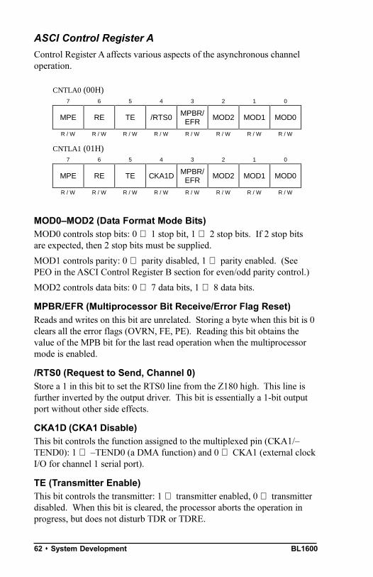
BL160062 s System Development
CNTLA0 (00H)7 6 5 4 3 2 1 0
MPE RE TE /RTS0 MPBR/EFR
MOD2 MOD1 MOD0
R / W R / W R / W R / W R / W R / W R / W R / W
CNTLA1 (01H)7 6 5 4 3 2 1 0
MPE RE TE CKA1D MPBR/EFR
MOD2 MOD1 MOD0
R / W R / W R / W R / W R / W R / W R / W R / W
ASCI Control Register A
Control Register A affects various aspects of the asynchronous channeloperation.
MOD0MOD2 (Data Format Mode Bits)MOD0 controls stop bits: 0 ⇒ 1 stop bit, 1 ⇒ 2 stop bits. If 2 stop bitsare expected, then 2 stop bits must be supplied.
MOD1 controls parity: 0 ⇒ parity disabled, 1 ⇒ parity enabled. (SeePEO in the ASCI Control Register B section for even/odd parity control.)
MOD2 controls data bits: 0 ⇒ 7 data bits, 1 ⇒ 8 data bits.
MPBR/EFR (Multiprocessor Bit Receive/Error Flag Reset)Reads and writes on this bit are unrelated. Storing a byte when this bit is 0clears all the error flags (OVRN, FE, PE). Reading this bit obtains thevalue of the MPB bit for the last read operation when the multiprocessormode is enabled.
/RTS0 (Request to Send, Channel 0)Store a 1 in this bit to set the RTS0 line from the Z180 high. This line isfurther inverted by the output driver. This bit is essentially a 1-bit outputport without other side effects.
CKA1D (CKA1 Disable)This bit controls the function assigned to the multiplexed pin (CKA1/TEND0): 1 ⇒ TEND0 (a DMA function) and 0 ⇒ CKA1 (external clockI/O for channel 1 serial port).
TE (Transmitter Enable)This bit controls the transmitter: 1 ⇒ transmitter enabled, 0 ⇒ transmitterdisabled. When this bit is cleared, the processor aborts the operation inprogress, but does not disturb TDR or TDRE.

BL1600 System Development s 63
CNTLB0 (02H) and CNTLB1 (03H)7 6 5 4 3 2 1 0
MPBT MP /CTSPS
PEO DR SS2 SS1 SS0
R / W R / W R / W R / W R / W R / W R / W R / W
Table 4-3. Baud Rate Divide Ratiosfor Source/Speed Select Bits
SS2 SS1 SS0 Divide Ratio
0 0 0 ÷ 1
0 0 1 ÷ 2
0 1 0 ÷ 4
0 1 1 ÷ 8
1 0 0 ÷ 16
1 0 1 ÷ 32
1 1 0 ÷ 64
1 1 1 external clock
RE (Receiver Enable)This bit controls the receiver: 1 ⇒ enabled, 0 ⇒ disabled. When this bit iscleared, the processor aborts the operation in progress, but does not disturbRDRF or the error flags.
MPE (Multiprocessor Enable)This bit (1 ⇒ enabled, 0 ⇒ disabled) controls the multiprocessor commu-nication mode which uses an extra bit for selective communication when anumber of processors share a common serial bus. This bit has effect onlywhen MP in ASCI Control Register B is set to 1. When this bit is 1, onlybytes with the MP bit on will be detected. Others are ignored. If this bit is0, all bytes received are processed. Ignored bytes do not affect the errorflags or RDRF.
ASCI Control Register B
Control register B configures the multiprocessor mode, parity and baud-rate selection for each channel.
SS (Source/Speed Select)Coupled with the prescaler (PS) and the divide ratio (DR), the SS bitsselect the source (internal or external clock) and the baud-rate divider, asshown in Table 4-3.
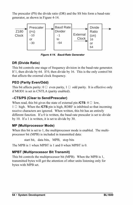
BL160064 s System Development
Prescaler(PS))10or)30
DivideRatio(DR)16or64
Baud RateDivider)1to)64
Z180Clock External
Clock
The prescaler (PS) the divide ratio (DR) and the SS bits form a baud-rategenerator, as shown in Figure 4-14.
Figure 4-14. Baud-Rate Generator
DR (Divide Ratio)This bit controls one stage of frequency division in the baud-rate generator.If 1, then divide by 64. If 0, then divide by 16. This is the only control bitthat affects the external clock frequency.
PEO (Parity Even/Odd)This bit affects parity: 0 ⇒ even parity, 1 ⇒ odd parity. It is effective onlyif MOD1 is set in CNTLA (parity enabled).
CTS/PS (Clear to Send/Prescaler)When read, this bit gives the state of external pin /CTS: 0 ⇒ low,1 ⇒ high. When the /CTS pin is high, RDRF is inhibited so that incomingreceive characters are ignored. When written, this bit has an entirelydifferent function. If a 0 is written, the baud rate prescaler is set to divideby 10. If a 1 is written, it is set to divide by 30.
MP (Multiprocessor Mode)When this bit is set to 1, the multiprocessor mode is enabled. The multi-processor bit (MPB) is included in transmitted data:
start bit, data bits, MPB, stop bits
The MPB is 1 when MPBT is 1 and 0 when MPBT is 0.
MPBT (Multiprocessor Bit Transmit)This bit controls the multiprocessor bit (MPB). When the MPB is 1,transmitted bytes will get the attention of other units listening only forbytes with MPB set.

BL1600 System Development s 65
Table 4-4. Baud Rates for ASCI Control Register B
ASCI ControlRegister B
Value
Baud Rate at9.216 MHz
(bps)
ASCI ControlRegister B
Value
Baud Rate at9.216 MHz
(bps)
00 57,600 20 19,200
01 28,800 21 9600
02 or 08 14,400 22 or 28 4800
03 or 09 7200 23 or 29 2400
04 or 0A 3600 24 or 2A 1200
05 or 0B 1800 25 or 2B 600
06 or 0C 900 26 or 2C 300
0D 450 2D 150
0E 225 2E 75
Table 4-4 relates ASCI Control Register B to the baud rate. The Z180 inthe BL1600 has a 9.216 MHz clock.

BL160066 s System Development
Blank

BL1600 Troubleshooting s 67
APPENDIX A:
TROUBLESHOOTING
Appendix A provides procedures for troubleshooting system hardware andsoftware. The sections include the following topics.
Out of the Box
Dynamic C Will Not Start
BL1600 Repeatedly Resets
Dynamic C Loses Serial Link
Common Programming Errors

BL160068 s Troubleshooting
Out of the BoxCheck the items listed below before starting development. Recheckingmay help to solve problems found during development.
Do not connect any boards with PLCBus, RS-485 or any other I/Odevices until you verify that the BL1600 runs standalone.
Verify that the entire system has good, low-impedance, separategrounds for analog and digital signals. The BL1600 is often connectedbetween the host PC and another device. Any differences in groundpotential can cause serious problems that are hard to diagnose.
Double-check the connecting cables. It is possible to reverse theconnections to the BL1600 headers.
Do not connect analog ground to digital ground anywhere.
Verify that the host PCs COM port works by connecting a known-goodserial device to the COM port. Remember that a PCs COM1/COM3and COM2/COM4 share interrupts. User shells and mouse software, inparticular, often interfere with proper COM-port operation. Forexample, a mouse running on COM1 can preclude running Dynamic Con COM3.
Use the Z-World power supply supplied with the Developers Kit. Ifanother power supply must be used, verify that it has enough capacityand filtering to support the BL1600.
Use the supplied Z-World cables. The most common fault of home-made cables is their failure to properly assert CTS at the RS-232 portof the BL1600. Without CTS being asserted, the BL1600s RS-232port will not transmit. You can assert CTS by either connecting theRTS signal of the PCs COM port or looping back the BL1600s RTS.

BL1600 Troubleshooting s 69
Dynamic C Will Not StartIf Dynamic C will not start, an error message on the Dynamic C screen (forexample, Target Not Responding or Communication Error), announcesa communication failure:
Wrong Baud Rate Either Dynamic Cs baud rate is not set correctlyor the BL1600s baud rate is not set correctly. Both baud rates must beidentical. The programming baud rate is set on the BL1600 byjumpering pins 12 or 34 on header J1 as described in Chapter 2.Dynamic Cs baud rate is set by the Serial Options command in theOPTIONS menu.
Wrong Communication Mode Both the PC and the BL1600 must beusing RS-232. Use Dynamic Cs Serial Options command in theOPTIONS menu to check and alter the protocol for the PC.
Wrong COM Port A PC generally has two serial ports, COM1 andCOM2. Specify the one used in the Dynamic C Serial Optionscommand in the OPTIONS menu. Use trial and error, if necessary.
Wrong Operating Mode The jumpers on pins 12 and 34 of headerJ1 must be configured for a programming option as described inChapter 2. Communication with Dynamic C is not possible with theBL1600 in run mode.
Wrong Memory Size Pins 510 on header J1 are used to specify thememory sizes of the EPROM and SRAM chips.
If all else fails, try connecting the serial cable to the BL1600 after power isapplied. Some RS-232 converters enter a nondestructive latch-up, and thiswill overcome that problem.
BL1600 Resets RepeatedlyWith the watchdog timer enabled by connecting pins 2728 on header J1,a system reset will occur every second if the watchdog timer is not hit atleast every 1.0 seconds. Dynamic C hits the timer, but a user programmust include calls to hitwd within the application to make sure the watch-dog timer is hit.
Dynamic C Loses Serial LinkIf the program disables interrupts for a period greater than 50 ms,Dynamic C will lose its serial link with the program. Make sure thatinterrupts are not disabled for longer than 50 ms.

BL160070 s Troubleshooting
Common Programming Errors Values for constants or variables out of range. Table A-1 lists accept-
able ranges for variables and constants.
Mismatched types. For example, the literal constant 3293 is of typeint (16-bit integer). However, the literal constant 3293.0 is of typefloat. Although Dynamic C can handle some type mismatches,avoiding type mismatches is the best practice.
Counting up from, or down to, one instead of zero. In software, ordinalseries often begin or terminate with zero, not one.
Confusing a functions definition with an instance of its use in a listing.
Not ending statements with semicolons.
Not inserting commas as required in functions parameter lists.
Leaving out ASCII space character between characters forming adifferent legalbut unwantedoperator.
Confusing similar-looking operators such as && with &,== with =, and // with /.
Inadvertently inserting ASCII nonprinting characters into a source-codefile.
Table A-1. Ranges of Dynamic CFunction Types
Type Range
int –32,768 (–215) to+32,767 (215 – 1)
long int −2,147,483,648 (−231) to+2147483647 (231 – 1)
float 1.18 × 10-38 to3.40 × 1038
char 0 to 255

BL1600 Specifications s 71
APPENDIX B:SPECIFICATIONS
Appendix B provides comprehensive BL1600 physical, electronic andenvironmental specifications.

BL160072 s Specifications
Table B-1. BL1600 General Specifications
Parameter Specification
Board Size4.52" × 4.175" × 1.0"(115 mm × 106 mm × 25 mm)
Operating Temperature -40°C to 70°C, may be stored at –55°C to 85°C
Humidity 5% to 95%, noncondensing
Power 9 V DC to 30 V DC, 150 mA, linear supply
Digital Inputs 12, TTL and CMOS compatible, 2.5 V digitalthreshold (8 additional inputs possible whenPLCBus is not used)
Digital Outputs
14, TTL and CMOS compatible — 7 of these arehigh-current outputs and can sink 100 mA each at50°C and 48 V DC; a single channel can sink upto 500 mA continuously at 25°C
Processor Z180
Clock 9.216 MHz
SRAM 32K standard, supports up to 512K
EPROM32K standard, may be replaced with 128K or256K flash EPROM
Flash EPROM May replace factory-installed EPROM
Counters Software-implementable
Serial PortsTwo RS-232 OR one RS-232 (with CTS/RTS)and one RS-485
Serial Rate Up to 57,600 bps
Watchdog Yes
Time/Date Clock Yes
Backup BatteryRenata CR2325RH 3 V DC lithium ion, rated life190 mA"h
Electrical and Mechanical SpecificationsTable B-1 lists electrical, mechanical, and environmental specifications forthe BL1600.

BL1600 Specifications s 73
BL1600 Mechanical Dimensions
Figure B-1 shows the mechanical dimensions for the BL1600.
0.2 typ(5)
0.160 dia, 4x(4)
4.52(115) ~0.35
(9)~
0.85
(22)
~1.
0(2
5)
0.2
(5)
3.6
(91)
3.9
(99)
4.17
5(1
06)
Figure B-1. BL1600 Dimensions

BL160074 s Specifications
DCIN
K
GND
485+
HC1
HC2
HC3
HC4
HC5
HC6
HC7
485–
H1 H2 H3
J2
H5
H4 J1
(soldered)
J3
Figure B-2. BL1600 Headers
Factory Default Jumper PositionsTable B-2 lists the jumper configurations for the BL1600 configurableheader (J1). The header locations are shown in Figure B-2.

BL1600 Specifications s 75
Table B-2. Standard BL1600 Jumper Settings on Header J1
Pin Group Description
Operating mode:
n.c. Run the program in RAM.
1-2 Place unit in programming mode at 9600 bps.
3-4Place unit in programming mode at baud ratespecified in EEPROM location 1.
1–4
1-2, 3-4Place unit in programming mode at19,200 bps (default)
EPROM sizes:
5-7, 6-8 32K (default)
6-8, 7-9 64K, 128K
5–10
7-9, 8-10 256K, 512K
11-13 Flash EPROM11, 13, 15
13-15 non-flash EPROM (default)
SRAM sizing:
12-14 32K or 128K SRAM. (default)
12, 14, 16
14-16 512K SRAM
17-19 Write-protect the upper half of the EEPROM.17, 19, 21
19-21 Write-enable the upper half of the EEPROM.
Serial communication:
18-2023-2524-26
One 5-wire RS-232 channel (Z180 Port 0) withRTS/CTS and one half-duplex RS-485 channel(Z180 Port 1). This is the default.
18, 20, 22,23–26
20-2223-24
Two 3-wire RS-232 channels. No RS-485.
27–28 Connect to enable the watchdog timer (default).

BL160076 s Specifications
Table B-3. BL1600 Header Functions
Header Function
H1 Digital inputs 0–11 (numbered 1–12 in the software).
H2Digital outputs. OUTB1–OUTB8 are 8-bit parallel.OUT1–OUT6, EN485 and SCL are individuallyselectable.
H3 RS-232 and programming port.
H4Miscellaneous lines. /USER1–/USER3, E, /DREQ0,/DREQ1, /INT2, /RESET.
H5PLCBus expansion connector — this connector supportsthe “LCD bus” as well. Use a 26-pin ribbon cable toattach PLCBus devices to the BL1600.
J2Screw terminal block — power, ground, RS-485, high-current outputs (HC1–HC7).
Table B-4. BL1600 Pin 1 Locations(in inches from corner with heat sink)
Header Location
H1 0.5, 3.8
H2 1.4, 3.8
H3 2.6, 3.8
H4 0.2, 3.2
H5 0.2, 1.6
Table B-3 lists the header functions for the input/output and serial commu-nication headers.
Table B-4 provides the relevant pin 1 locations for these headers.

BL1600 Specifications s 77
.mA150V5
−−
=INV
PI (B-1)
Installation Concepts
Connectors
Ideally, you should place a single, solid conductor in a screw clampterminal. Bare copper, particularly if exposed to the air for a long periodbefore installation, can become oxidized. The oxide can cause a high-resistance (~20 Ω) connection, especially if the clamping pressure is notsufficient. To avoid this, use tinned wires, clean, shiny copper wire, orcrimp the connector.
If you are using multiple conductors or stranded wire, consider solderingthe wire bundle or using a crimp connector to avoid a loss of contactpressure to a spontaneous rearrangement of the wire bundle at a later time.Soldering may make the wire subject to fatigue failure at the junction withthe solder if there is flexing or vibration.
Power Consumption and Heat Dissipation
With the standard heat sink, the total thermal resistance at the voltageregulator is about 15.2°C/W. The smaller heat sink has a thermal resis-tance of about 25.2°C/W. The maximum junction temperature of the regu-lator is 125°C.
If the BL1600 is drawing 3 W, the regulator (with the large heat sink) willoperate at
TA + 3 × 15.2°C = 95.6°C
for an ambient temperature, TA, of 50°C. The maximum power dissipation
would be
WT = (125°C 50°C)/(15.2°C/W) = 4.93 W for the large heat sink
WT = (125°C 50°C) /(25.2°C/W) = 2.98 W for the small heat sink
at 50°C. Additional power draw is possible if forced convection cooling isprovided.
The BL1600 draws about 150 mA from the total current available.Therefore, the current available to external accessories or additionalonboard devices is
If the input voltage is 12 V, the total current available to accessories is560 mA with the standard heat sink (5 W) and 270 mA with the small heatsink (3 W). For a 24 V input, the total current available is 90 mA with thestandard heat sink, and no power is left over with the small heat sink.These values are approximate.

BL160078 s Specifications
For additional information on maximum operatingconditions for the BL1600 high-voltage drivers, callZ-World Technical Support at (530) 757-3737.
(
High-Voltage DriversTable B-5 lists the high-voltage driver characteristics when sinking driversor sourcing drivers are used.
Sinking Driver
The sinking-driver IC can handle a maximum of 1.38 A (500 mA for anychannel), or 75 mA per channel on average if all channels are ON, at 60°C.The absolute maximum power that the driver IC can dissipate depends onseveral factors. The sinking ICs saturation voltage is 1.6 V DC max perchannel.
The sinking drivers source voltage must range from 2 V to 48 V DC.
Table B-5. High-Voltage Driver Characteristics
Characteristic
Sinking Driver
Sourcing Driver
IC ULN2003A UDN2985A
Number of Channels 7 8
Max. Current per Channel(all channels ON)
75 mA @ 60°C
125 mA @ 50°C
75 mA @ 60°C
125 mA @ 50°C
Voltage Source Range 2 V to 48 V DC 3 V to 30 V DC
Package Power Dissipation 2.2 W @ 25°C 2.2 W@ 25°C
Max. Current(all channels ON)
1.38 A 1.38 A
Max. Collector-EmitterVoltage (VCE)
1.6 V 1.6 V
Derating 18 mW/°C(55°C/W)
18 mW/°C(55°C/W)
Output Flyback Diode (K) Yes Yes
Max. Diode-Drop Voltage(K)
2 V DC 2 V DC
FD

BL1600 Specifications s 79
For more information on sinking and sourcing high-voltagedrivers, refer to the Motorola (DL128) or Allegro (AMS502Z) data books.
$
See Appendix D, Sinking and Sourcing Drivers, for moreinformation on installing and using sourcing drivers.$
The sourcing drivers source voltage must range from 3 V to30 V DC. The minimum output sustaining voltage is 15 VDC. Operating the driver at more than 15 V without provid-ing for energy dissipation may destroy the driver when aninductive load is connected.
Sourcing Driver
The sourcing-driver IC can handle a maximum of 1.38 A (250 mA for anychannel), or 75 mA per channel on average if all channels are ON, at 60°C.The sourcing IC can dissipate a maximum of 2.2 W. The saturationvoltage is 1.6 V DC max per channel.

BL160080 s Specifications

BL1600 Prototyping Board s 81
APPENDIX C:
PROTOTYPING BOARD
BL160082 s Prototyping Board
IntroductionThe BL1600 was designed to allow customers to build expansion boardsthat piggyback on the BL1600. Z-Worlds Prototyping Board lets youdevelop such circuitry efficiently. The Prototyping Board is an array ofuncommitted pads on 0.1" centers. Five power rails bring ±15 V, +5 V,and ground to the pads. The rails are spaced with pads judiciouslyconnected so that you easily place and connect 300-mil and 600-mil DIPs.A large section of the board is available for discrete components.
The Prototyping Board has direct connections to the BL1600s input/output headers: the PLCBus port, expansion header, digital inputs, digitaloutputs, and serial ports. The BL1600 can access up to 48 addresses on anexpansion board.
Features Compactness
The Prototyping Board fits directly over the BL1600, providing a soundfoundation for your design.
Power Rails
There are five power rails on board allowing ICs and components easyaccess to various operating voltages. Each power rail supplies +15 V,-15 V, +5 V, and ground.
Direct Header Connections
All the BL1600 headers connect directly the Prototyping Board.
Sea of Pads
An array of pads is provided for DIPs and discrete components. Pads andpower rails are arranged and interconnected so that it is easy to place andconnect 300-mil and 600-mil DIPs.
Extra Pads
Extra pads bring out signals from the PLCBus and the expansion headerfor easier soldering.
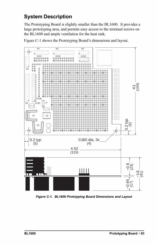
BL1600 Prototyping Board s 83
System DescriptionThe Prototyping Board is slightly smaller than the BL1600. It provides alarge prototyping area, and permits easy access to the terminal screws onthe BL1600 and ample ventilation for the heat sink.
Figure C-1 shows the Prototyping Boards dimensions and layout.
Figure C-1. BL1600 Prototyping Board Dimensions and Layout
~0.
65(1
7)~
0.9
(23)
~1.
6(4
1)
4.1
(104
)
0.2
typ
(5)
0.160 dia, 3x(4)
4.52(115)
0.2 typ(5)
U1
U3
H5 H105 J1
U2
H106
H107
H101
H4
H1
H102
H2
H103
H3
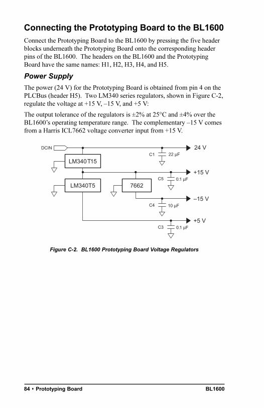
BL160084 s Prototyping Board
LM340T15
DCIN
LM340T5 7662
C1
C4
C5
C3
24 V
+15 V
15 V
+5 V
22 µF
0.1 µF
10 µF
0.1 µF
Connecting the Prototyping Board to the BL1600Connect the Prototyping Board to the BL1600 by pressing the five headerblocks underneath the Prototyping Board onto the corresponding headerpins of the BL1600. The headers on the BL1600 and the PrototypingBoard have the same names: H1, H2, H3, H4, and H5.
Power Supply
The power (24 V) for the Prototyping Board is obtained from pin 4 on thePLCBus (header H5). Two LM340 series regulators, shown in Figure C-2,regulate the voltage at +15 V, 15 V, and +5 V:
The output tolerance of the regulators is ±2% at 25°C and ±4% over theBL1600s operating temperature range. The complementary 15 V comesfrom a Harris ICL7662 voltage converter input from +15 V.
Figure C-2. BL1600 Prototyping Board Voltage Regulators

BL1600 Prototyping Board s 85
15 V+15 V+5 V
+5 V
+15 V
15 V
J1
H106 GND
Power Rails
Power Rails
The five power rails on the Prototyping Board each supply +15 V , 15 V,+5 V, and ground. A small section of the Prototyping Board (next toheader H106) has labels indicating the repeating sequence of the voltages.Figure C-3 shows the power rails.
Figure C-3. BL1600 Prototyping Board Power Rails
The pads on the Prototyping Board have various diameters. All the padsalong a power rail have a 60-mil outer diameter and a 37-mil inner diame-ter. Most other pads are 65/45, except the three columns of pads nearestthe ICL7662 converter, which have pads that have an outer diameter of70 mil and an inner diameter of 50 mil. These larger pads are ideal forcomponents, such as diodes, with thicker legs.
Note that all ground pins have square pads on the power rails.

BL160086 s Prototyping Board
GN
D+
5 V
+15
V–1
5 V
GN
D+
5 V
+15
V–1
5 V
(a) GND and 5 V on Top Side (b) +15 V and 15 V on Bottom Side
Figure C-4. BL1600 Prototyping Board ConnectionsAmong Adjacent Pads
Figure C-5. DIP Placement Along Power Rails
If you look closely at the top side of the board, you will note that somepads are connected to adjacent pads. This pattern is laid out with DIPplacement in mind. You can place either 300-mil or 600-mil DIPs in manydifferent positions and still have DIP pins connected to the adjacent pads.This makes it easy to connect them to other components. For a standard300-mil DIP, a power rail fits in between its two rows of pins; for DIPs600 mils in width, two power rails fit between its pins. This arrangementgives the DIPs easy access to the different operating voltages.
Figure C-4 illustrates this arrangement.
Figure C-5 shows the top left part wired to a ground pad through anadjacent connected pad. The middle part is wired to +5 V. The larger parton the right is wired to +15 V.
BL1600 Prototyping Board s 87
Table C-1. BL1600 Prototyping Board Header Signals
Headers
BL1600 PrototypingBoard
Signals
H1 H101 Digital inputs IN00–IN11
H2 H102Digital outputs OUT1–OUT6, EN485, SCL,OUTB1–OUTB8
H3 H103 RS-232, /RX0, /TX0, /RX1, /TX1
H5 H105PLCBus (4 address lines, 8 data lines, read, write,24 V DC, etc.)
— H106Address and data lines with read and write linesfrom the PLCBus
H4 H107PLCBus expansion bus (/USER1–/USER3, E,/DREQ0–/DREQ1, /INT2, /RESET)
$
$
Interface with BL1600Headers H1, H2, H3, H4 and H5 connect directly to the BL1600, bringingall relevant signals of the BL1600 to the Prototyping Board. Theseheaders represent the PLCBus, the digital I/O, the serial channels, and thePLCBus expansion bus. H101, H102, H103, and H105 duplicate thedigital input, output, serial, and PLCBus headers, respectively, permittingeasier soldering. Header H106 duplicates the address and data lines of thePLCBus as well as its read and write signals. Header H107 duplicates thesignals of H4.
The signals on these headers are listed in Table C-1.
Chapter 4, System Development, discusses these headersignals in more detail.
Z-Worlds Technical Note 102, BL1600 Prototyping Board,describes the design an A/D converter using the PrototypingBoard, and discusses the integration of the software, firmwareand hardware.

BL160088 s Prototyping Board
Prototyping Board Pinouts
Figure C-6 shows the pinouts for the BL1600 Prototyping Board.
Figure C-6. BL1600 Prototyping Board Signals
IN00IN02IN04IN06IN08IN10GND
135791113
2468
101214
IN01IN03IN05IN07IN09IN11
+5 V
H101
OUTB7
OUT1OUT3OUT5
EN485
OUTB1OUTB3OUTB5
135791113151719
2468
101214161820
GND
OUTB8
OUT2OUT4OUT6SCLGNDOUTB2OUTB4OUTB6
+5 V
+5 V
H102
13579
2468
10
/TX0 /RX1 or /CTS0/RX0 /TX1 or /RTS0
H103
GND
1357
2468
/USR2 /INT2/USR3 /DR0
/USR1
E /DR1
H107/RST
D0X
/AT
A3XA2X
D6XD4XD2X
135791113151719
2468
101214161820
GND
A1X
H105
+5 V
/WRX/RDX
212325
222426
+5 V
D1X
+24 VGNDGND
GNDD7XD5XD3X
GND
LCDXA0X
/STBX
GND
12245678910
H106
11121314
D2X
A2X
A0XD7X
D5XD4XD3X
A3X
D6X
/WRX
D1XD0X
A1X
/RDX

BL1600 Sinking and Sourcing Drivers s 89
APPENDIX D:
SINKING AND SOURCING DRIVERS

BL160090 s Sinking and Sourcing Drivers
BL1600 Series Sinking and Sourcing OutputsThe BL1600 Series controllers are normally supplied with ULN2003sinking drivers. Figure D-1 shows a typical sinking driver output configu-ration.
Sourcing outputs are possible by replacing the factory-installed sinkingdriver chips with sourcing output drivers (UDN2985). The UDN2985sourcing driver chip is capable of sourcing a maximum of 75 mA peroutput.
ULN2003
K
ExternalLoad
FreewheelDiode
+DC
I # 500 mA/channel
Fly
back
Cur
rent
Pat
h
VS
AT #
1.6
V D
CFigure D-1. BL1600 Sinking Driver Output

BL1600 Sinking and Sourcing Drivers s 91
Figure D-2 shows a typical sourcing driver output.
Z-World also offers all BL1600 Series controllers forquantity orders with factory-installed sourcing drivers.For ordering information, call your Z-World SalesRepresentative at (530) 757-3737.
(
ExternalLoad
UDN2985
K
+DC
FreewheelDiode
VS
AT #
1.6
V D
C
Figure D-2. BL1600 Series Sourcing Driver Output

BL160092 s Sinking and Sourcing Drivers
DCIN
K
GND
485+
HC1
HC2
HC3
HC4
HC5
HC6
HC7
485–
H1 H2 H3
J2
H5
H4 J1
J3
U10
H.V
. Driv
er
Figure D-3. Location of BL1600 Sinking Driver
Installing Sourcing Driver
Figure D-3 shows the location of the driver to be changed.
Pay particular attention to the orientation of the chip when changing thedriver. Exercise caution when installing sourcing drivers in the field.
1. Be sure power is removed from the controller.
2. Remove the ULN2003 sinking driver from the IC socket.
3. Install the UDN2985 sourcing driver chip into the IC socket.

BL1600 Sinking and Sourcing Drivers s 93
Using Output DriversThe common supply for all seven channels supplied by a driver chip iscalled K, and is labeled as such on header J2. K must be powered upto allow proper operation.
The K connection performs two vital functions to the high-voltage drivercircuitry on the BL1600.
1. K supplies power to driver circuitry inside the driver chip.
2. K also allows a diode internal to the driver chip to snub voltagetransients produced during the inductive kick associated with switchinginductive loads. (Relays, solenoids, and speakers are examples ofinductive loads.)
Long leads may present enough induction to also produce large potentiallydamaging voltage transients. The anodes of the protection diodes for eachchannel are common, and so only one voltage supply can be used for allhigh-voltage driver loads.
The following points summarize the functions of K.
K provides power to the driver chip circuitry.
K provides clamping for all high-voltage driver loads.
It is mandatory to connect K regardless of whether sourcing or sinking.
The loads supply must have a common ground with all other suppliesin your system.
All loads must use same supply voltage.
Refer to Figure D-4 and Figure D-5 when connecting K.

BL160094 s Sinking and Sourcing Drivers
To BL1600 K Connection
To BL1600 High-Voltage Output
LOAD
To Load Power (+DC source)
BL1600 K ConnectionSinking Configuration
Figure D-4. BL1600 K Connections (Sinking Configuration)
To BL1600 K Connection
To BL1600 High-Current Output
BL1600 K ConnectionSourcing Configuration
LOAD
To Load Power (+DC source)
Figure D-5. BL1600 K Connections (Sourcing Configuration)
K must be connected to the power supply used for the high-voltage load. See Figure D-4 and Figure D-5.

BL1600 PLCBus s 95
APPENDIX E:
PLCBUS
Appendix E provides the pin assignments for the PLCBus, describes theregisters, and lists the software drivers.

BL160096 s PLCBus
PLCBus OverviewThe PLCBus is a general-purpose expansion bus for Z-World controllers.The PLCBus is available on the BL1200, BL1600, BL1700, PK2100, andPK2200 controllers. The BL1000, BL1100, BL1300, BL1400, andBL1500 controllers support the XP8300, XP8400, XP8600, and XP8900expansion boards using the controllers parallel input/output port. TheBL1400 and BL1500 also support the XP8200 and XP8500 expansionboards. The ZB4100s PLCBus supports most expansion boards, exceptfor the XP8700 and the XP8800. The SE1100 adds expansion capabilityto boards with or without a PLCBus interface.
Table E-1 lists Z-Worlds expansion devices that are supported on thePLCBus.
Multiple expansion boards maybe linked together and con-nected to a Z-World controllerto form an extended system.
Figure E-1 shows the pin layoutfor the PLCBus connector.
Table E-1. Z-World PLCBus Expansion Devices
Device Description
EXP-A/D12 Eight channels of 12-bit A/D converters
SE1100 Four SPDT relays for use with all Z-World controllers
XP8100 Series 32 digital inputs/outputs
XP8200 “Universal Input/Output Board”—16 universal inputs, 6 high-current digital outputs
XP8300 Two high-power SPDT and four high-power SPST relays
XP8400 Eight low-power SPST DIP relays
XP8500 11 channels of 12-bit A/D converters
XP8600 Two channels of 12-bit D/A converters
XP8700 One full-duplex asynchronous RS-232 port
XP8800 One-axis stepper motor control
XP8900 Eight channels of 12-bit D/A converters
24
13
6 58 7
10 912 1114 1316 1518 1720 1922 2124 2326 25
GNDD7XD5XD3XD1X
LCDXA0X
GND
GND attention /ATstrobe /STBXGNDA3XGNDA2XGNDA1X
/RDXVCC (+5 V)
D0X/WRX
D4XD2X
D6X
+24 V(+5 V) VCC
Figure E-1. PLCBus Pin Diagram

BL1600 PLCBus s 97
The PLCBus consists of the following lines.
/STBXnegative-going strobe.
A1XA3Xthree control lines for selecting bus operation.
D0XD3Xfour bidirectional data lines used for 4-bit operations.
D4XD7Xfour additional data lines for 8-bit operations.
/ATattention line (open drain) that may be pulled low by any device,causing an interrupt.
The PLCBus may be used as a 4-bit bus (D0XD3X) or as an 8-bit bus(D0XD7X). Whether it is used as a 4-bit bus or an 8-bit bus depends onthe encoding of the address placed on the bus. Some PLCBus expansioncards require 4-bit addressing and others (such as the XP8700) require8-bit addressing. These devices may be mixed on a single bus.
Two independent buses, the LCD bus and the PLCBus, exist on the singleconnector.
The LCD bus consists of the following lines.
LCDXpositive-going strobe. /RDXnegative-going strobe for read. /WRXnegative-going strobe for write. A0Xaddress line for LCD register selection. D0X-D7Xbidirectional data lines (shared with expansion bus).
The LCD bus is used to connect Z-Worlds OP6000 series interfaces or todrive certain small liquid crystal displays directly. Figure E-2 illustratesthe connection of an OP6000 interface to a controller PLCBus.
Yellow wireon top
PLCBus HeaderNote position of connector
relative to pin 1.
From OP6000KLB Interface CardHeader J2
Pin 1
Figure E-2. OP6000 Connection to PLCBus Port

BL160098 s PLCBus
Table E-2. PLCBus Registers
Register Address A3 A2 A1 Meaning
BUSRD0 C0 0 0 0 Read data, one way
BUSRD1 C2 0 0 1Read data, anotherway
BUSRD2 C4 0 1 0 Spare, or read data
BUSRESET C6 0 1 1Read this register toreset the PLCBus
BUSADR0 C8 1 0 0First address nibbleor byte
BUSADR1 CA 1 0 1Second addressnibble or byte
BUSADR2 CC 1 1 0Third address nibbleor byte
BUSWR CE 1 1 1 Write data
There are eight registers corresponding to the modes determined by buslines A1X, A2X, and A3X. The registers are listed in Table E-2.
Writing or reading one of these registers takes care of all the bus details.Functions are available in Z-Worlds software libraries to read from orwrite to expansion bus devices.
To communicate with a device on the expansion bus, first select a registerassociated with the device. Then read or write from/to the register. Theregister is selected by placing its address on the bus. Each device recog-nizes its own address and latches itself internally.
A typical device has three internal latches corresponding to the threeaddress bytes. The first is latched when a matching BUSADR0 is de-tected. The second is latched when the first is latched and a matchingBUSADR1 is detected. The third is latched if the first two are latched anda matching BUSADR2 is detected. If 4-bit addressing is used, then thereare three 4-bit address nibbles, giving 12-bit addresses. In addition, aspecial register address is reserved for address expansion. This address, ifever used, would provide an additional four bits of addressing when usingthe 4-bit convention.
If eight data lines are used, then the addressing possibilities of the busbecome much greatermore than 256 million addresses according to theconventions established for the bus.

BL1600 PLCBus s 99
Table E-3. First-Level PLCBus Address Coding
First Byte Mode Addresses Full Address Encoding
– – – – 0 0 0 0– – – – 0 0 0 1– – – – 0 0 1 0– – – – 0 0 1 1
4 bits × 3 256256256256
0000 xxxx xxxx0001 xxxx xxxx0010 xxxx xxxx0011 xxxx xxxx
– – – x 0 1 0 0– – – x 0 1 0 1– – – x 0 1 1 0– – – x 0 1 1 1
5 bits × 3 2,0482,0482,0482,048
x0100 xxxxx xxxxxx0101 xxxxx xxxxxx0110 xxxxx xxxxxx0111 xxxxx xxxxx
– – x x 1 0 0 0– – x x 1 0 0 1
6 bits × 3 16,38416,384
xx1000 xxxxxx xxxxxxxx1001 xxxxxx xxxxxx
– – x x 1 0 1 0 6 bits × 1 4 xx1010
– – – – 1 0 1 1 4 bits × 1 1 1011 (expansion register)
x x x x 1 1 0 0 8 bits × 2 4,096 xxxx1100 xxxxxxxx
x x x x 1 1 0 1 8 bits × 3 1M xxxx1101 xxxxxxxx xxxxxxxx
x x x x 1 1 1 0 8 bits × 1 16 xxxx1110
x x x x 1 1 1 1 8 bits × 1 16 xxxx1111
Place an address on the bus by writing (bytes) to BUSADR0, BUSADR1and BUSADR2 in succession. Since 4-bit and 8-bit addressing modesmust coexist, the lower four bits of the first address byte (written toBUSADR0) identify addressing categories, and distinguish 4-bit and 8-bitmodes from each other.
There are 16 address categories, as listed in Table E-3. An x indicatesthat the address bit may be a 1 or a 0.
This scheme uses less than the full addressing space. The mode notationindicates how many bus address cycles must take place and how many bitsare placed on the bus during each cycle. For example, the 5 × 3 modemeans three bus cycles with five address bits each time to yield 15-bitaddresses, not 24-bit addresses, since the bus uses only the lower five bitsof the three address bytes.

BL1600100 s PLCBus
SHBUS1 SHBUS1+1SHBUS0 SHBUS0+1 SHBUS0+2 SHBUS0+3
Bus expansion BUSADR0 BUSADR1 BUSADR2
Table E-4. Allocation of Registers
A1 A2 A3 Meaning
000j 000j xxxjdigital output registers, 64 registers64 × 8 = 512 1-bit registers
000j 001j xxxj analog output modules, 64 registers
000j 01xj xxxjdigital input registers, 128 registers128 × 4 = 512 input bits
000j 10xj xxxj analog input modules, 128 registers
000j 11xj xxxj 128 spare registers (customer)
001j xxxj xxxj 512 spare registers (Z-World)
j controlled by board jumperx controlled by PAL
Z-World provides software drivers that access the PLCBus. To allowaccess to bus devices in a multiprocessing environment, the expansionregister and the address registers are shadowed with memory locationsknown as shadow registers. The 4-byte shadow registers, which are savedat predefined memory addresses, are as follows.
Before the new addresses or expansion register values are output to thebus, their values are stored in the shadow registers. All interrupts that usethe bus save the four shadow registers on the stack. Then, when exiting theinterrupt routine, they restore the shadow registers and output the threeaddress registers and the expansion registers to the bus. This allows aninterrupt routine to access the bus without disturbing the activity of abackground routine that also accesses the bus.
To work reliably, bus devices must be designed according to the followingrules.
1. The device must not rely on critical timing such as a minimum delaybetween two successive register accesses.
2. The device must be capable of being selected and deselected withoutadversely affecting the internal operation of the controller.
Allocation of Devices on the Bus
4-Bit Devices
Table E-4 provides the address allocations for the registers of 4-bitdevices.
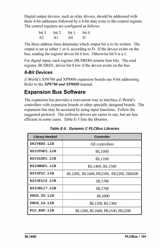
BL1600 PLCBus s 101
Table E-5. Dynamic C PLCBus Libraries
Library Needed Controller
DRIVERS.LIB All controllers
EZIOTGPL.LIB BL1000
EZIOLGPL.LIB BL1100
EZIOMGPL.LIB BL1400, BL1500
EZIOPLC.LIB BL1200, BL1600, PK2100, PK2200, ZB4100
EZIOPLC2.LIB BL1700
EZIOBL17.LIB BL1700
PBUS_TG.LIB BL1000
PBUS_LG.LIB BL1100, BL1300
PLC_EXP.LIB BL1200, BL1600, PK2100, PK2200
Digital output devices, such as relay drivers, should be addressed withthree 4-bit addresses followed by a 4-bit data write to the control register.The control registers are configured as follows
bit 3 bit 2 bit 1 bit 0A2 A1 A0 D
The three address lines determine which output bit is to be written. Theoutput is set as either 1 or 0, according to D. If the device exists on thebus, reading the register drives bit 0 low. Otherwise bit 0 is a 1.
For digital input, each register (BUSRD0) returns four bits. The readregister, BUSRD1, drives bit 0 low if the device exists on the bus.
8-Bit Devices
Z-Worlds XP8700 and XP8800 expansion boards use 8-bit addressing.Refer to the XP8700 and XP8800 manual.
Expansion Bus SoftwareThe expansion bus provides a convenient way to interface Z-Worldscontrollers with expansion boards or other specially designed boards. Theexpansion bus may be accessed by using input functions. Follow thesuggested protocol. The software drivers are easier to use, but are lessefficient in some cases. Table E-5 lists the libraries.

BL1600102 s PLCBus
There are 4-bit and 8-bit drivers. The 4-bit drivers employ the followingcalls.
void eioResetPlcBus()
Resets all expansion boards on the PLCBus. When using this call,make sure there is sufficient delay between this call and the first accessto an expansion board.
LIBRARY: EZIOPLC.LIB, EZIOPLC2.LIB, EZIOMGPL.LIB.
void eioPlcAdr12( unsigned addr )
Specifies the address to be written to the PLCBus using cyclesBUSADR0, BUSADR1, and BUSADR2.
PARAMETER: addr is broken into three nibbles, and one nibble iswritten in each BUSADRx cycle.
LIBRARY: EZIOPLC.LIB, EZIOPLC2.LIB, EZIOMGPL.LIB.
void set16adr( int adr )
Sets the current address for the PLCBus. All read and write operationsaccess this address until a new address is set.
PARAMETER: adr is a 16-bit physical address. The high-ordernibble contains the value for the expansion register, and the remainingthree 4-bit nibbles form a 12-bit address (the first and last nibbles mustbe swapped).
LIBRARY: DRIVERS.LIB.
void set12adr( int adr )
Sets the current address for the PLCBus. All read and write operationsaccess this address until a new address is set.
PARAMETER: adr is a 12-bit physical address (three 4-bit nibbles)with the first and third nibbles swapped.
LIBRARY: DRIVERS.LIB.
void eioPlcAdr4( unsigned addr )
Specifies the address to be written to the PLCBus using only cycleBUSADR2.
PARAMETER: addr is the nibble corresponding to BUSADR2.
LIBRARY: EZIOPLC.LIB, EZIOPLC2.LIB, EZIOMGPL.LIB.

BL1600 PLCBus s 103
void set4adr( int adr )
Sets the current address for the PLCBus. All read and write operationsaccess this address until a new address is set.
A 12-bit address may be passed to this function, but only the last fourbits will be set. Call this function only if the first eight bits of theaddress are the same as the address in the previous call to set12adr.
PARAMETER: adr contains the last four bits (bits 811) of thephysical address.
LIBRARY: DRIVERS.LIB.
char _eioReadD0( )
Reads the data on the PLCBus in the BUSADR0 cycle.
RETURN VALUE: the byte read on the PLCBus in the BUSADR0cycle.
LIBRARY: EZIOPLC.LIB, EZIOPLC2.LIB, EZIOMGPL.LIB.
char _eioReadD1( )
Reads the data on the PLCBus in the BUSADR1 cycle.
RETURN VALUE: the byte read on the PLCBus in the BUSADR1cycle.
LIBRARY: EZIOPLC.LIB, EZIOPLC2.LIB, EZIOMGPL.LIB.
char _eioReadD2( )
Reads the data on the PLCBus in the BUSADR2 cycle.
RETURN VALUE: the byte read on the PLCBus in the BUSADR2cycle.
LIBRARY: EZIOPLC.LIB, EZIOPLC2.LIB, EZIOMGPL.LIB.
char read12data( int adr )
Sets the current PLCBus address using the 12-bit adr, then reads fourbits of data from the PLCBus with BUSADR0 cycle.
RETURN VALUE: PLCBus data in the lower four bits; the upper bitsare undefined.
LIBRARY: DRIVERS.LIB.

BL1600104 s PLCBus
char read4data( int adr )
Sets the last four bits of the current PLCBus address using adr bits 811, then reads four bits of data from the bus with BUSADR0 cycle.
PARAMETER: adr bits 811 specifies the address to read.
RETURN VALUE: PLCBus data in the lower four bits; the upper bitsare undefined.
LIBRARY: DRIVERS.LIB.
void _eioWriteWR( char ch)
Writes information to the PLCBus during the BUSWR cycle.
PARAMETER: ch is the character to be written to the PLCBus.
LIBRARY: EZIOPLC.LIB, EZIOPLC2.LIB, EZIOMGPL.LIB.
void write12data( int adr, char dat )
Sets the current PLCBus address, then writes four bits of data to thePLCBus.
PARAMETER: adr is the 12-bit address to which the PLCBus is set.
dat (bits 03) specifies the data to write to the PLCBus.
LIBRARY: DRIVERS.LIB.
void write4data( int address, char data )
Sets the last four bits of the current PLCBus address, then writes fourbits of data to the PLCBus.
PARAMETER: adr contains the last four bits of the physical address(bits 811).
dat (bits 03) specifies the data to write to the PLCBus.
LIBRARY: DRIVERS.LIB.
The 8-bit drivers employ the following calls.
void set24adr( long address )
Sets a 24-bit address (three 8-bit nibbles) on the PLCBus. All read andwrite operations will access this address until a new address is set.
PARAMETER: address is a 24-bit physical address (for 8-bit bus)with the first and third bytes swapped (low byte most significant).
LIBRARY: DRIVERS.LIB.

BL1600 PLCBus s 105
void set8adr( long address )
Sets the current address on the PLCBus. All read and write operationswill access this address until a new address is set.
PARAMETER: address contains the last eight bits of the physicaladdress in bits 1623. A 24-bit address may be passed to this function,but only the last eight bits will be set. Call this function only if the first16 bits of the address are the same as the address in the previous call toset24adr.
LIBRARY: DRIVERS.LIB.
int read24data0( long address )
Sets the current PLCBus address using the 24-bit address, then readseight bits of data from the PLCBus with a BUSRD0 cycle.
RETURN VALUE: PLCBus data in lower eight bits (upper bits 0).
LIBRARY: DRIVERS.LIB.
int read8data0( long address )
Sets the last eight bits of the current PLCBus address using address bits1623, then reads eight bits of data from the PLCBus with a BUSRD0cycle.
PARAMETER: address bits 1623 are read.
RETURN VALUE: PLCBus data in lower eight bits (upper bits 0).
LIBRARY: DRIVERS.LIB.
void write24data( long address, char data )
Sets the current PLCBus address using the 24-bit address, then writeseight bits of data to the PLCBus.
PARAMETERS: address is 24-bit address to write to.
data is data to write to the PLCBus.
LIBRARY: DRIVERS.LIB.
void write8data( long address, char data )
Sets the last eight bits of the current PLCBus address using address bits1623, then writes eight bits of data to the PLCBus.
PARAMETERS: address bits 1623 are the address of the PLCBusto write.
data is data to write to the PLCBus.
LIBRARY: DRIVERS.LIB.

BL1600106 s PLCBus
Blank

BL1600 EEPROM s 107
APPENDIX F:
EEPROM

BL1600108 s EEPROM
EEPROM ParametersThe onboard EEPROM (electrically erasable, programmable, read-onlymemory) is used to store the constants and parameters listed in Table F-1.The five bytes presently in use determine the operation of the BL1600board when it starts up.
The EEPROM has 512 bytes. The upper 256 bytes can be written to onlywhen pins 19 and 21 on header J1 are connected. Connect pins 17 and 19on header J1 to write-protect the EEPROM.
Baud Rate
When the EEPROM is first initialized, the baud rate is set to 57,600 bps.The next section outlines the procedure to change these parameters.
Startup Mode
In programming mode, the board initializes Serial Port 0 for Dynamic C.When set for run mode, the board attempts to execute a user-writtenprogram stored in battery-backed RAM or in EPROM.
The baud rate code determines the serial communication rate at which theBL1600 attempts to communicate with the PC and Dynamic C.
Table F-1. BL1600 EEPROM Assignments
Address Definition
0Startup Mode — if 1, enter program mode; if 8, executeloaded program at startup.
1
Programming baud rate in multiples of 1200 bps. The fac-tory default is 48, meaning 57,600 bps. This location ap-plies only if J1 pins 1–2 are not connected and J1 pins 3–4are connected.
0x100Unit “serial number” in BCD time and date with the fol-lowing format: second, minutes, hours, day, month, andyear.
0x108Microprocessor clock speed in multiples of 1200 Hz (16bits). (This value is 7680 for a 9.216 MHz clock speed.)
0x16C
Long coefficient relating speed of microprocessor clockrelative to speed of real-time clock. Nominal value is107,374,182, which is 1/40 of a second microprocessorclock time on the scale where 232 is 1 second. This requires4 bytes of EEPROM, stored least byte first.

BL1600 EEPROM s 109
Clock Speed
The clock speed code is used by the BL1600 to compute parametersnecessary to set the serial port. The clock speed is also used by severalDynamic C library functions.
Changing Parameters Stored in EEPROM1 Install jumper across pins 1921 on header J1.
2 Use the ee_wr function to change the parameters.
3 Reset the BL1600 by interrupting power or by momentarily connectingpins 910 on header H4.
4 Reconnect pins 1719 on header J1. The BL1600 will automaticallyuse the new mode or baud rate specified for the next restart. The boardwill continue to operate with the new setting until the EEPROM ischanged.
Follow the above procedures to change any of the parameters listed inTable F-1. First, perform the procedure for one of these parameters, thenrepeat the procedure for the other parameters.
Library RoutinesThe following library routines can be used to read and write the EEPROM.
int ee_rd( int address );
int ee_wr( int address, char value );
The function ee_rd returns the data value in the lower byte, and thefunction ee_wr writes the character value at address. The functions returna negative value if there is a hardware problem. If this happens withee_wr, try writing again after checking pins 1921 on header J1 to makesure the EEPROM is write-enabled. Repeated negative values may beindicative of a worn-out EEPROM. A write-protection violation does notwear out the EEPROM.
These routines each require about 2.5 ms to execute. They are not re-entrant, that is, only one routine at a time will run.
The EEPROM has a rated lifetime of only 10,000 writes(unlimited reads). Do not write the EEPROM from within aloop. The EEPROM should be written to only in response to ahuman request for each write.
!

BL1600110 s EEPROM
Blank

BL1600 Memory, I/O Map, and Interrupt Vectors s 111
APPENDIX G: MEMORY,I/O MAP, AND INTERRUPT VECTORS
Appendix G provides detailed information on memory, provides an I/Omap, and lists the interrupt vectors.

BL1600112 s Memory, I/O Map, and Interrupt Vectors
BL1600 MemoryFigure G-1 shows the memory map of the 1M address space.
Figure G-1. Memory Map of 1M Address Space
Figure G-2 shows the memory map within the 64K virtual space.
Figure G-2. Memory Map of 64K Virtual Space
The various registers in the input/output (I/O) space can be accessed inDynamic C by the symbolic names listed below. These names are treatedas unsigned integer constants. The Dynamic C library functions inportand outport access the I/O registers directly.
data_value = inport( CNTLA0 );
outport( CNTLA0, data_value );
UNITIALIZEDDATA
USER CODE
LIBRARY
RAM
ROM
RAM
ROM
UNUSED
RAM-Based ROM-Based
0
STACK
XMEM64K
UNITIALIZEDDATA
USER CODE
LIBRARY
UNUSED
STACK
XMEM
512K
1024K
Socket U8RAM
Socket U7EPROM
0x00000
0x80000

BL1600 Memory, I/O Map, and Interrupt Vectors s 113
Memory and Input/Output Cycle Timing
There are two types of memory cycles that need to be considered: standardmemory cycles and Load Instruction Register (LIR) cycles. LIR cycles,which fetch the op code, have the most critical timing requirement. Thememory access time, t, in nanoseconds, can be calculated for these cyclesusing
t = 2T - 95 , (G-1)
where T is the period of a clock cycle. Figure G-3 shows these cycles withand without a wait state.
Figure G-3. Memory Cycles for 9.216 MHz ProcessorWith and Without a Wait State
The standard version of the PAL generates a wait state only during the LIRcycles. Therefore it is called a ½ wait state PAL.
T1 T2 TwT3
address
T1 T2 T3
address
data data
TAD = 70 ns TAD = 70 nsTDRS = 25 ns TDRS = 25 ns
0 wait states 1 wait state
/ME
/RD
/WR
0 wait access time = 2T - 95 ns 1 wait access time = 3T - 95 ns
= 122 ns for 9.216 MHz clock = 230 ns for 9.216 MHz clock

BL1600114 s Memory, I/O Map, and Interrupt Vectors
Table G-1. Memory Access Times(ns)
Clock Frequency EPROM SRAM
9.216 MHz, 0 wait states 122 176
9.216 MHz, 1 wait state 230 283
TwT1 T2
A0A15
/IOE
/RD
/WR
T3Tw1
D0D7 write
D0D7 read
The standard memory cycles require an access time of 2.5T - 95 nanosec-onds. Table G-1 lists the memory access times required for various clockfrequencies and wait states.
The memory access times in Table G-1 were calculated assuming that LIRcycles only take place in EPROM. These access times are conservative,and no problem should be encountered by using an EPROM with amemory access time that is more than the time listed in Table G-1.
Input/Output Cycle TimingCustomer peripheral devices are usually interfaced as I/O devices. This isconvenient because only eight address lines need to be decoded in mostcases. Figure G-4 shows how wait cycles are inserted in I/O cycles. Atleast one wait cycle (T
W) is always inserted. Up to four additional wait
states can be inserted, depending on the setup of the wait-state generator.One additional wait state, the default number (T
W1), is shown in Figure G-4.
Figure G-4. Inserting Wait Cycles in I/O Cycles

BL1600 Memory, I/O Map, and Interrupt Vectors s 115
Table G-2. BL1600 Execution Times for Dynamic C
Operation Execution Time(µs)
DMA copy (per byte) 0.73
Integer assignment (i=j;) 3.4
Integer add (j+k;) 4.4
Integer multiply (j*k;) 18
Integer divide (j/k;) 90
Floating add (p+q;) (typical) 85
Floating multiply (p*q;) 113
Floating divide (p/q;) 320
Long add (l+m;) 28
Long multiply (l*m;) 97
Long divide (l/m;) 415
Floating square root (sqrt(q);) 849
Floating exponent (exp(q);) 2503
Floating cosine (cos(q);) 3049
Execution Timing
The times reported in Table G-2 were measured using Dynamic C and theyreflect the use of Dynamic C libraries. The time required to fetch thearguments from memory, but not to store the result, is included in thetimings. The times are for a 9.216 MHz clock with 0 wait states.
The execution times can be adjusted proportionally for clock speeds otherthan 9.216 MHz. Operations involving one wait state will slow theexecution speed about 25%.

BL1600116 s Memory, I/O Map, and Interrupt Vectors
Memory Map
Input/Output Select Map
The Dynamic C library functions IBIT, ISET and IRES in the BIOS.LIBlibrary allow bits in the I/O registers to be tested, set, and cleared. Both16-bit and 8-bit I/O addresses can be used.
Z180 Internal Input/Output Registers Addresses 0x000x3F
The internal registers for the I/O devices built into to the Z180 processoroccupy the first 40 (hex) addresses of the I/O space. These addresses arelisted in Table G-3.
Table G-3. Z180 Internal I/O Registers Addresses 0x00–0x3F
Address Name Description
0x00 CNTLA0 Serial Channel 0, Control Register A
0x 01 CNTLA1 Serial Channel 1, Control Register A
0x02 CNTLB0 Serial Channel 0, Control Register B
0x03 CNTLB1 Serial Channel 1, Control Register B
0x04 STAT0 Serial Channel 0, Status Register
0x05 STAT1 Serial Channel 1, Status Register
0x06 TDR0 Serial Channel 0, Transmit Data Register
0x07 TDR1 Serial Channel 1, Transmit Data Register
0x08 RDR0 Serial Channel 0, Receive Data Register
0x09 RDR1 Serial Channel 1, Receive Data Register
0x0A CNTR Clocked Serial Control Register
0x0B TRDR Clocked Serial Data Register
0x0C TMDR0L Timer Data Register Channel 0, least
0x0D TMDR0H Timer Data Register Channel 0, most
0x0E RLDR0L Timer Reload Register Channel 0, least
0x0F RLDR0H Timer Reload Register Channel 0, most
0x10 TCR Timer Control Register
0x11–0x13 — Reserved
0x14 TMDR1L Timer Data Register Channel 1, least
0x15 TMDR1H Timer Data Register Channel 1, most
0x16 RLDR1L Timer Reload Register Channel 1, least
0x17 RLDR1H Timer Reload Register Channel 1, most
continued…

BL1600 Memory, I/O Map, and Interrupt Vectors s 117
Table G-3. Z180 Internal I/O Registers Addresses 0x00–0x3F (concluded)
Address Name Description
0x18 FRC Free-running counter
0x19–0x1F — Reserved
0x20 SAR0L DMA source address Channel 0, least
0x21 SAR0H DMA source address Channel 0, most
0x22 SAR0B DMA source address Channel 0, extra bits
0x23 DAR0L DMA destination address Channel 0, least
0x24 DAR0H DMA destination address Channel 0, most
0x25 DAR0B DMA destination address Channel 0, extra bits
0x26 BCR0L DMA Byte Count Register Channel 0, least
0x27 BCR0H DMA Byte Count Register Channel 0, most
0x28 MAR1L DMA Memory Address Register Channel 1, least
0x29 MAR1H DMA Memory Address Register Channel 1, most
0x2A MAR1BDMA Memory Address Register Channel 1, extrabits
0x2B IAR1L DMA I/O Address Register Channel 1, least
0x2C IAR1H DMA I/O Address Register Channel 1, most
0x2D — Reserved
0x2E BCR1L DMA Byte Count Register Channel 1, least
0x2F BCR1H DMA Byte Count Register Channel 1, most
0x30 DSTAT DMA Status Register
0x31 DMODE DMA Mode Register
0x32 DCNTL DMA/WAIT Control Register
0x33 IL Interrupt Vector Low Register
0x34 ITC Interrupt/Trap Control Register
0x35 — Reserved
0x36 RCR Refresh Control Register
0x37 — Reserved
0x38 CBR MMU Common Base Register
0x39 BBR MMU Bank Base Register
0x3A CBAR MMU Common/ Bank Area Register
0x3B–0x3D — Reserved
0x3E OMCR Operation Mode Control Register
0x3F ICR I/O Control Register

BL1600118 s Memory, I/O Map, and Interrupt Vectors
Table G-4. Epson 72421 Timer Registers 0x4000–0x400F
Address Name Data Bits Description
0x4000 SEC1 D7–D0 seconds
0x4001 D7–D0 10 seconds
0x4002 D7–D0 minutes
0x103 D7–D0 10 minutes
0x4004 D7–D0 hours
0x4005 D7–D0 10 hours
0x4006 D7–D0 days
0x4007 D7–D0 10 days
0x4008 D7–D0 months
0x4009 D7–D0 10 months
0x400A D7–D0 years
0x400B D7–D0 10 years
0x400C D7–D0 day of week
0x400D TREGD D7–D0 Register D
0x400E D7–D0 Register E
0x400F D7–D0 Register F
Epson 72421 Timer Registers 0x40000x400F
Table G-4 lists the Epson 72421 timer registers.

BL1600 Memory, I/O Map, and Interrupt Vectors s 119
Table G-5. Other I/O Addresses
Address Name Data Bits Description
0x040 SDA_W D7 EEPROM serial data, write. Bit 7.
0x080 LCDRDLCDWR
D0–D7 LCD read/write register, control.
0x081 LCDRD+1LCDWR+1
D0–D7 LCD read/write register, data.
0x110 INENLO D0–D7 Bits 0–7 represent digital inputs 0–7.
0x111 INENHI D0–D3 Bits 0–3 represent digital inputs 8–11.
0x111 CONFIG D4 Bit 4 represents pins 1-2 on header J1.
0x111 SDA_R D5 Read bit 5 to get EEPROM SDA line.
0x111 NMI D6 Bit 6 is the power-failure (NMI) state.
0x111 CONFIG D7 Bit 7 represents pins 3-4 on header J1.
0x120 DRV1 D0 High-current output 1 (HC1). Bit 0.This output also appears on H2.
0x121 DRV2 D0 High-current output 2 (HC2). Bit 0.This output also appears on H2.
0x122 DRV3 D0 High-current output 3 (HC3). Bit 0.This output also appears on H2.
0x123 DRV4 D0 High-current output 4 (HC4). Bit 0.This output also appears on H2.
0x124 DRV5 D0 High-current output 5 (HC5). Bit 0.This output also appears on H2.
0x125 DRV6 D0 High-current output 6 (HC6). Bit 0.This output also appears on H2.
0x126 ENB485 D0 Set bit 0 to enable RS-485 transmis-sion. Clear bit 0 to disable. The linecontrolled by this bit can also be usedas a digital output channel and a high-current channel (HC7).
continued…
Other Addresses
Table G-5 lists the other registers.

BL1600120 s Memory, I/O Map, and Interrupt Vectors
Table G-5. Other I/O Addresses (concluded)
Address Name Data Bits Description
0x127 SCL D0 EEPROM clock bit. Set the clock highby setting bit 0 of this address, and lowby clearing bit 0.
0x130 OUTBYTE D0–D7 8-bit parallel TTL-level digital output(OUTB1–OUTB8 on the schematic).
0x150 USER1 — Base address of expansion registergroup 1. These 16 registers have ad-dresses 0x150 to 0x15F. Addressingany of these registers makes /USER1assert.
0x160 USER2 — Base address of expansion registergroup 2. These 16 registers have ad-dresses 0x160 to 0x16F. Addressingany of these registers makes /USER2assert.
0x170 USER3 — Base address of expansion registergroup 3. These 16 registers have ad-dresses 0x170 to 0x17F. Addressingany of these registers makes /USER3assert.
0x1C0 WDOG — Watchdog is “hit” (J1:27-28 enableswatchdog) by reading or writing thisaddress.

BL1600 Memory, I/O Map, and Interrupt Vectors s 121
Table G-6. Interrupt Vectors for Z180 Internal Devices
Address Name Description
0x00 INT1_VEC Expansion bus attention INT1 vector.
0x02 INT2_VEC INT2 vector, can be jumpered to the outputof the real-time clock for a periodic interrupt
0x04 PRT0_VEC PRT Timer Channel 0
0x06 PRT1_VEC PRT Timer Channel 1
0x08 DMA0_VEC DMA Channel 0
0x0A DMA1_VEC DMA Channel 1
0x0C CSIO_VEC Clocked Serial I/O
0x0E SER0_VEC Asynchronous Serial Port Channel 0
0x10 SER1_VEC Asynchronous Serial Port Channel 1
Interrupt VectorsTable G-6 presents a suggested interrupt vector map. Most of theseinterrupt vectors can be altered under program control. The addresses aregiven here in hex, relative to the start of the interrupt vector page, asdetermined by the contents of the I-register. These are the default interruptvectors set by the boot code in the Dynamic C EPROM.
To vector an interrupt to a user function in Dynamic C, use a directivesuch as the following.
#INT_VEC 0x10 myfunction
The above example causes the interrupt at offset 10H (Serial Port 1 of theZ180) to invoke the function myfunction(). The function must bedeclared with the interrupt keyword, as shown below.
interrupt myfunction() ...
Refer to the Dynamic C manuals for further details on interruptfunctions.$

BL1600122 s Memory, I/O Map, and Interrupt Vectors
Nonmaskable Interrupts
Power Failure InterruptsThe following sequence of events takes place when power fails.
1. The power-failure nonmaskable interrupt (NMI) is triggered when theunregulated DC input voltage falls below approximately 7.9 V.
2. The system reset is triggered when the regulated +5 V supply fallsbelow 4.65 V. The reset remains enabled as the voltage falls further.At this point, the chip select for the SRAM is forced high (standbymode).
3. The time/date clock and SRAM are switched to the lithium backupbattery as the regulated voltage falls below the battery voltage ofapproximately 3 V.
The following function shows how to handle a power-failure interrupt.
#JUMP_VEC NMI_VEC myint
interrupt retn myint()body of interrupt routinewhile(!IBIT(WDO,0))
// input voltage is still below the threshold// that triggered the NMI
return; // if just a power glitch, return
Normally, a power-failure interrupt routine will not return, but will executethe shutdown code and then enter a loop until the +5 V voltage falls lowenough to trigger a reset. However, the voltage might fall low enough in abrownout situation to trigger a power failure interrupt, but not lowenough to reset, resulting in an endless hangup. Bit 0 of WDO is 0 whenthe voltage level is below the NMI threshold, and 1 otherwise. If this bitindicates that the low-voltage condition has reversed itself, then the power-fail routine can restart execution. If a lowbut not fatally lowvoltagepersists, then you will have to decide what action to take, if any.
A situation similar to a brownout will occur if the power supply is over-loaded. For example, when an LED is turned on, the voltage supplied tothe Z180 may dip below 7.9 V. The interrupt routine does a shutdown.This turns the LED off, clearing the problem. However, the cause of theoverload may persist, and the system will oscillate, alternately experienc-ing an overload and then resetting. To correct this situation, you need toget a larger power supply.

BL1600 Memory, I/O Map, and Interrupt Vectors s 123
Do not forget the interaction between the watchdog timer and the power-failure interrupt. If a brownout causes an extended stay in the power-failure interrupt routine, the watchdog can time out and cause a systemrestart.
A few milliseconds of computing time remain when the +5 V supply fallsbelow 4.5 V, even if power is abruptly cut off from the board. The amountof time depends on the size of the capacitors in the power supply. Thestandard wall transformer provides about 10 ms. If the power cable isabruptly removed from the BL1600 side, only the capacitors on the boardare available and the computing time is reduced to a few hundred micro-seconds. These times can vary considerably depending on the systemconfiguration and loads on the 5 V or 9 V power supplies.
The interval between the power-failure detection and entry to the power-failure interrupt routine is approximately 100 µs, or less if Dynamic CNMI communications is not in use.
Testing power-failure interrupt routines presents some problems. Nor-mally, a power-failure interrupt routine disables interrupts. Probably thebest test method is to leave messages in battery-backed memory to trackthe execution of the power-failure routines. Use a variable transformer tosimulate brownouts and other types of power-failure conditions.
The power-failure interrupt must be disabled if an external +5 V powersupply is used.
Jump Vectors
These special interrupts occur in a different manner. Instead of loading theaddress of the interrupt routine from the interrupt vector, these interruptscause a jump directly to the address of the vector, which will contain ajump instruction to the interrupt routine. This example illustrates a jumpvector.
0x66 nonmaskable power-failure interrupt
Since nonmaskable interrupts (NMI) can be used for Dynamic C communi-cations, an interrupt vector for power failure is normally stored just in frontof the Dynamic C program. Use the command
#JUMP_VEC NMI_VEC name
to store the vector here.
The Dynamic C communication routines relay to this vector when the NMIis caused by a power failure rather than by a serial interrupt.

BL1600124 s Memory, I/O Map, and Interrupt Vectors
Table G-7. Interrupt Priorities
Interrupt Priorities
(Highest Priority) Trap (illegal instruction)
NMI (nonmaskable interrupt)
INT 0 (maskable interrupts, Level 0; three modes)
INT 1 (maskable interrupts, Level 1; PLCBusattention line interrupt)
INT 2 (maskable interrupts, Level 2)
PRT Timer Channel 0
PRT Timer Channel 1
DMA Channel 0
DMA Channel 1
Clocked Serial I/O
Z180 Serial Port 0
(Lowest Priority) Z180 Serial Port 1
Interrupt Priorities
Table G-7 lists the interrupt priorities.

BL1600 Power Management s 125
APPENDIX H:
POWER MANAGEMENT
Appendix H provides information about power management and handlingpower failures.

BL1600126 s Power Management
ADM691 Power SupervisorThe ADM691 power-supervisor IC (U13) helps the system survive powerfluctuations and outages. It provides these vital services.
Power-on reset.
The ADM691 generates the power-on reset for the BL1600 by holding/RESET low until the ICs internal comparators sense that VCC hasrisen above 4.65 V (the ICs preset reset threshold ).
RAM protection
The ADM691 gates the decoded RAM-select line, /RAMCEIN, to theRAMs chip-enable line, /RAMCE, whenever VCC is above the resetthreshold and VBAT. When VCC falls below the threshold, theADM691 deasserts /RAMCE to prevent spurious writing to the RAM.
Watchdog timer
The ADM691 provides a watchdog timer that guards against system orsoftware faults by resetting the BL1600 if the software does not hitthe watchdog timer input, WDI, at least every 1.0 seconds. Hit thewatchdog timer by calling the function hitwd.
The supervisors watchdog output, /WDO, connects to the Z180s RXS/CTSI- interrupt line; /WDO is at a logic zero level after a watchdogreset and a logic 1 after a power-on reset.
Nonmaskable interrupt
The ADM691 generates a nonmaskable interrupt, /NMI, from itspower-fail output, /PFO, if the unregulated DC input, normally 9 V to12 V DC, falls below 7.9 V, giving the BL1600 advanced warning of animpending power failure so that it can execute shutdown routines. Thevoltage divider, R1-R2, determines this 7.9 V level.
/NMI also connects to the Z180 via multiplexer U2 to allow yoursoftware to monitor the /NMI line after the nonmaskable interrupt, andto recover from temporary low-input voltage conditions or brown-outs.
Backup-battery switchover
The ADM691 switches the RAM over to battery power if VCC fallsbelow the batterys voltage

BL1600 Power Management s 127
Power Failure ManagementFigure H-1 shows the power-failure detection circuitry of the BL1600.
Figure H-1. BL1600 Power-Failure Detection Circuit
Power Failure Sequence
The following events occur as the input power fails.
1. The ADM691 first triggers a power-failure /NMI (nonmaskableinterrupt) when the unregulated DC input voltage falls below approxi-mately 7.9 V (as determined by the voltage divider R1R2), allowingthe power-failure routine to store important state data during theholdup interval, t
H.
2. At some point, the raw input voltage level will drop below the regulat-ed voltage level required by the regulators dropout voltage, whereuponthe regulated output will begin to droop. The ADM691 next triggers asystem reset, /RESET, when the regulated +5 V supply falls below≈4.65 V. The ADM691 forces the chip-enable line of the SRAM high(standby mode). Thus your power-failure routine uses the holdupinterval (the time between steps 1 and 2), t
H, to store important state
data.
3. The SRAM switches to the backup battery when the regulated voltagefalls below the batterys voltage, preserving the RAMs data.
4. The ADM691 keeps /RESET enabled until the regulated voltage dropsbelow 1 V. At this point the ADM691 ceases operating. By this time,the portion of the circuitry not battery-backed should have long sinceceased functioning.
PFI
/PFO /NMI
DCIN
R1
R2
IC691
Z180
/RES
/RESET
Data Bus
D6
U13 U15
VBAT
VBAT

BL1600128 s Power Management
Figure H-2 shows the power-failure sequence.
Figure H-2. Power-Failure Sequence
Of course, if the DC input voltage continues to decrease, then the control-ler will just power down. The routine calls hitwd to make sure that thewatchdog does not time out and thereby reset the processor. The controllercan continue to run, after a fashion, at low voltages, and might not be ableto detect the low-voltage condition because the Z180s /NMI input needs tosee a high-to-low transition edge.
A situation similar to a brownout will occur if the power supply is over-loaded. In such a case, when a high-current load turns on, the raw voltagesupplied to the Z180 may dip below 7.9 V. In response, the interruptroutine does a shutdown. This shutdown turns off the high-current load,clearing the problem. However, if the cause of the overload persists, thesystem will hunt, alternately experiencing an overload and then resetting.To correct this situation, you must get a larger power supply.
1.0
2.0
9.0
8.0
7.0
6.0
5.0
4.0
3.0
I
UnregulatedDC
Regulated+5 V
691Asserts PFO
691AssertsRESET
691 CeasesOperation
tH
Power Fails
Time
CSlope = C/-I
Dropout Voltage
Vol
tage
(V
)

BL1600 Power Management s 129
Holdup Time
A few milliseconds of computing time remain until the regulated +5 Vsupply falls below ∼4.65 V, even if the power cuts off abruptly. Theamount of time depends on the size of the capacitors in the power supply.The standard power supply included with Z-Worlds Developers Kitprovides about 10 ms. If the power cable is removed abruptly from theBL1600 side, then only the capacitors on the board are available, reducingcomputing time to a few hundred microseconds. These times can varyconsiderably depending on the systems configuration and loads on the 5 Vor 9 V supplies.
The interval between detection of the power failure detection and entry tothe power-failure interrupt routine is approximately 6 µs or less
Z-World cannot predict how much time will actually be available to saveimportant state data. The ratio of the raw DC power supplys outputcapacitors value to the circuits current draw determines the actualduration of the holdup time, t
H.
Multiple Power-Line Insults
This simple setup can fail when multiple power fluctuations follow eachother rapidlya common occurrence. If the BL1600s Z180 microproces-sor receives multiple /NMIs, it will overwrite an internal register, making acorrect return from the first /NMI impossible. Also, depending on thenumber of fluctuations of the raw DC input (and hence, the number ofstacked /NMIs), the microprocessors stack could possibly overflow,corrupting the programs code or data.
When the Z180 senses an /NMI, it saves the program counter (PC) on itsprocessor stack. The Z180 copies the maskable interrupt flag, IEF1, toIEF2 and zeroes IEF1. The Z180 will restore IEF2s saved state informa-tion when it executes a RETN (return from nonmaskable interrupt)instruction.

BL1600130 s Power Management
Sample Program to Handle Power Failure
Z-World recommends the following routine to handle an /NMI. Theroutines monitor the state of the /PFO line via U2 and the data bus todetermine if the brownout condition is continuing or if the power hasreturned to normal levels. If you use this routine, you will never have toworry about multiple power-failure /NMIs because this routine simplynever returns from the first /NMI unless the power returns.
main()...
...
char dummy[24]; // reserve dummy stack// for /NMI processing
...
#define NMI_BIT 6 // routine will test data// bit 6 to determine// state of /NMI line
#JUMP_VEC NMI_VEC myint
#asm
myint::ld sp,dummy+24 ; force stack pointer
; to top of "dummy"; array to prevent; overwriting of code; or data
do whatever service, within allowable execution time
loop:call hitwd ; make sure no
; watchdog reset; during brownout
ld bc,NMI ; load the read-NMI; register to bc
in a,(c) ; read the read-NMI; register to /PFO
bit NMI_BIT, a ; check /PFO statusjr z,loop ; wait until brownout
; condition clears
timeout: ; then... a tight loop; to force a watchdog; timeout
jp timeout ; which will reset the; Z180
#endasm

BL1600 Battery s 131
APPENDIX I:
BATTERY
Appendix I provides information about the onboard lithium backupbattery.

BL1600132 s Battery
Battery Life and Storage ConditionsThe battery on the BL1600 controller will provide at least 9,000 hours ofbackup time for the onboard real-time clock and SRAM. However,backup time longevity is affected by many factors, including the amount oftime the controller is unpowered and the SRAM size. Most systems areoperated on a continuous basis, with the battery supplying power to thereal-time clock and the SRAM during power outages and/or during routinemaintenance. The time estimate reflects the shelf life of a lithium ionbattery with occasional use rather than the ability of the battery to powerthe circuitry full time.
The battery has a capacity of 190 mA·h. At 25°C, the real-time clock draws3 µA when idle, and the 32K SRAM draws 2 µA. If the BL1600 wereunpowered 100 percent of the time, the battery would last 38,000 hours(4.3 years).
To maximize the battery life, the BL1600 should be stored at roomtemperature in the factory packaging until field installation. Take care thatthe BL1600 is not exposed to extreme temperature, humidity, and/orcontaminants such as dust and chemicals.
To ensure maximum battery shelf life, follow proper storage procedures.Replacement batteries should be kept sealed in the factory packaging atroom temperature until installation. Protection against environmentalextremes will help maximize battery life.
Replacing Soldered Lithium BatteryUse the following steps to replace the battery.
1. Locate the three pins on the bottom side of the printed circuit boardthat secure the battery to the board.
2. Carefully de-solder the pins and remove the battery. Use a soldersucker to clean up the holes.
3. Install the new battery and solder it to the board. Use only a RenataCR2325RH or its equivalent.

BL1600 Battery s 133
Battery Cautions Caution (English)
There is a danger of explosion if the battery is incorrectly replaced.Replace only with the same or equivalent type recommended by themanufacturer. Dispose of used batteries according to themanufacturers instructions.
Warnung (German)
Explosionsgefahr durch falsches Einsetzen oder Behandein derBatterie. Nur durch gleichen Typ oder vom Hersteller empfohlenenErsatztyp ersetzen. Entsorgung der gebrauchten Batterien gemäb denAnweisungen des Herstellers.
Attention (French)
Il y a danger dexplosion si la remplacement de la batterie est incorrect.Remplacez uniquement avec une batterie du même type ou dun typeéquivalent recommandé par le fabricant. Mettez au rebut les batteriesusagées conformément aux instructions du fabricant.
Cuidado (Spanish)
Peligro de explosión si la pila es instalada incorrectamente. Reemplacesolamente con una similar o de tipo equivalente a la que el fabricanterecomienda. Deshagase de las pilas usadas de acuerdo con lasinstrucciones del fabricante.
Waarschuwing (Dutch)
Explosiegevaar indien de batterij niet goed wordt vervagen.Vervanging alleen door een zelfde of equivalent type als aanbevolendoor de fabrikant. Gebruikte batterijen afvoeren als door de fabrikantwordt aangegeven.
Varning (Swedish)
Explosionsfära vid felaktigt batteribyte. Använd samma batterityp elleren likvärdigt typ som rekommenderas av fabrikanten. Kassera använtbatteri enligt fabrikantens instruktion.

BL1600134 s Battery
Blank

BL1600 Index s 135
INDEX
Symbols
#define .................................... 40#INT_VEC ......................... 45, 121#JUMP_VEC ..................... 122, 123+5 V power supply ................... 127
holdup time .......................... 129/AT .............................................. 97/CTS .................................... 60, 64/CTS0 ......................................... 44/DCD0 ........................................ 60/DREQ0 ............................... 33, 34/DREQ1 ............................... 33, 34/INT0 .......................................... 34/INT1 .......................................... 34/INT2 ................................... 33, 34/PFO ................................ 126, 130/RAMCE ................................... 126/RAMCEIN ............................... 126/RDX .......................................... 97/RESET ............. 33, 34, 126, 127/RTS0 ......................................... 62/STBX ........................................ 97/USER1/USER3 ....................... 33/WDO ....................................... 126/WRX .......................................... 97=(assignment)
use .......................................... 704-bit bus operations ... 97, 98, 1005 × 3 addressing mode ............... 998-bit bus operations ... 97, 99, 1019th-bit address mode .................. 519th-bit binary communication ..54, 559th-bit transmission ................... 51
A
A0X ............................................ 97A1X, A2X, A3X ................... 97, 98
addressesencoding................................. 99modes ..................................... 99PLCBus .................................. 99
ADM691 (power supervisor IC) 126applications
relays ...................................... 31solenoids ................................ 31stepping motors ...................... 31
ASCI ............................ 60, 62, 63Control Register A ................. 62Control Register B ................. 63status registers ........................ 60
ASCII charactersand modem commands .......... 44
asynchronouschannels ................................. 62serial ports ............................. 58
asynchronous serial communicationinterface. See ASCI
attention line .............................. 97
B
background routine .................. 100backup battery .......................... 127battery
cautions ................................ 132replacing .............................. 132
battery-backed clock .................. 38battery-backed RAM .....................
.................... 13, 26, 44, 123baud rate ................................... 24,
.. 32, 46, 54, 57, 58, 64, 65serial ports ............................. 57
bidirectional data lines ............... 97BL1600 ...................................... 12
default communication rate ... 21features ................................... 13power supply .......................... 18setup ....................................... 18

BL1600136 s Index
CKA1/TEND0 ............................. 62CKA1D ....................................... 62Clear to Send/Prescaler .............. 64clock
battery-backed ....................... 38external .................................. 58frequency
system ............................... 13,.......... 32, 57, 58, 63, 64, 65
millisecond ............................. 39real-time .................... 13, 38, 39time/date ....... 13, 38, 122, 127
CMOS ........................................ 30CNTLA ....................................... 61CNTLB ....................................... 63CNTLB0 ..................................... 57CNTLB1 ..................................... 57COMMAND mode
modem communication .......... 44command protocol
master-slave ........................... 51common problems
programming errors ............... 70wrong COM port ................... 68
communicationDynamic C ........................... 123function libraries .................... 56initialization routines ............. 45RS-232 . 13, 32, 43, 44, 46, 47RS-485 ............................ 13, 30,
........ 32, 51, 52, 54, 55, 56serial ................ 13, 30, 32, 43,
.. 44, 45, 46, 52, 54, 55, 57,
. 58, 59, 60, 62, 63, 65, 116interrupts ............................ 43master-slave ......... 51, 54, 55
compile-time interrupt directive .. 50connections
RS-485 two-wire network ...... 52connectors
26-pin PLCBuspin assignments .................. 96
screw ...................................... 77costatements ............................... 39
block diagramBL1600 .................................. 30
brownouts ..... 122, 123, 126, 128buffer
receive . 43, 44, 46, 47, 54, 55initialization ....................... 46reading ............................... 46
transmit .................... 43, 47, 55initialization ....................... 46writing ................................ 47
buscontrol registers ................... 101digital inputs ........................ 101expansion .............................. 96,
........... 97, 98, 99, 100, 1018-bit drivers ..................... 104addresses .......................... 100devices .................... 100, 101functions 102, 103, 104, 105rules for devices ............... 100software drivers ............... 101
LCD ....................................... 97operations
4-bit .................... 97, 98, 1008-bit ........................... 97, 101
PLCBus ........................... 43, 45BUSADR0 ........................... 98, 99BUSADR1 ........................... 98, 99BUSADR2 ........................... 98, 99BUSADR3 ....................... 104, 105BUSRD0 ....... 101, 102, 103, 105BUSRD1 ......................... 101, 102BUSWR ................................... 102
C
CARRIAGE RETURNas modem command terminator . 44
CE compliance ........................... 16check sum .................... 51, 54, 55
computing .............................. 50check_opto_command ............ 54checking for modem commands .. 49CKA1 ......................................... 62CKA1 disable ............................. 62

BL1600 Index s 137
counter input .............................. 37counters
virtual timer ........................... 42CPLC.LIB .................................. 41CRC ............................. 51, 54, 55
computing .............................. 50CSI/O .................................. 50, 61CTS ................ 43, 44, 46, 59, 61CTS enable ................................ 61CTS/PS ...................................... 64CTS1 .......................................... 61cyclic redundancy check. See CRC
D
D0XD7X ................................... 97Data Carrier Detect .................... 60Data Format Mode Bits ............. 62DATA mode
modem communication .......... 44date and time .............................. 38DCD0 ........................... 58, 59, 61DCD0 line to ground .................. 59Ddelay_100ms ......................... 49deciphering modem commands ... 49default jumper settings ............... 74delay
in slave response .................... 55modem communication ... 49, 50
delay_1sec ............................. 49DelayMs .................................... 39DelaySec .................................. 39Developer's Kit .......................... 15development tools ...................... 15Dget_modem_command ............ 49DIGIN1...DIGIN12 .................... 41digital inputs ... 13, 30, 36, 39, 41
pinout ..................................... 31digital outputs . 13, 30, 36, 39, 41
high-voltage driver specifications78
pinout ..................................... 31dimensions
BL1600 .................................. 73Dinit_uart ...................... 43, 45
Dinit_z0 .................... 43, 45, 48Dinit_z1 ........................... 43, 45diodes
protective ............................... 31DIP relays .................................. 96direct drivers .............................. 36disabling interrupts .................... 50
DMA channels ....................... 50Z180 serial channels 0 and 1 . 50
disabling the RS-485 driver ....... 56display
liquid crystal .......................... 97divide ratio ................................. 64Dkill_z0 .................................. 47DMA
channels ................................. 37disabling interrupts ............ 50
counter ................................... 37interrupts ................................ 37request ............................. 33, 34
DMA0Count ................................ 37DMA1Count ................................ 37DMAFLAG0 .................................. 37DMASnapShot ........................... 37downloading data ......... 43, 44, 48downloading programs ....... 45, 50DR .............................................. 64Dread_z0 .................................. 47Dread_z01ch ........................... 46Dreset_z0rbuf ....................... 47Dreset_z0tbuf ....................... 47Drestart_z0modem ................. 49drivers
high-current ............................ 31sinking .................................... 15software ................................. 36
direct .................................. 36expansion bus .................. 101expansion bus 8-bit .......... 104high-level ........................... 36indirect ........................ 36, 41low-level ............................ 36relay ................................. 101virtual ..... 36, 39, 40, 41, 42

BL1600138 s Index
driverssoftware
virtualfunction library ....... 40, 41variables ......................... 40
sourcing ................................. 15installation ......................... 92
DRIVERS.LIB .................. 35, 101DTR ............................................ 44Dwrite_z0 ................................ 47Dwrite_z01ch ......................... 47Dxmodem_z0down ..................... 48Dxmodem_z0up ......................... 48Dynamic C .......................... 15, 21
communications ................... 123libraries .................................. 35programming BL1600 ........... 24programming port .................. 50serial options .......................... 21standard version ..................... 35will not start ........................... 69
Dz0_circ_int ......................... 49Dz0modem_chk ......................... 49Dz0send_prompt ..................... 47
E
E .......................................... 33, 34echo option .................. 43, 44, 46ee_rd ...................................... 109ee_wr ...................................... 109EEPROM .............. 13, 30, 50, 57
baud rate .............................. 108changing stored parameters ... 109clock speed .......................... 109constants .............................. 121initialization ......................... 108library routines ..................... 109operating mode .................... 108
programming .................... 108run .................................... 108
writeslifetime ............................. 109
EFR ............................................ 61EFR bit ....................................... 61
eioPlcAdr12 ......................... 102eioReadD0 .............................. 103eioReadD1 .............................. 103eioReadD2 .............................. 103eioResetPlcBus ................... 102eioWriteWR ........................... 104electrical specifications .............. 72EN485 .......................... 30, 31, 36environmental specifications ..... 72EPROM ......................................13,
........... 24, 25, 26, 38, 39, 45copyright ................................ 27flash ................................ 26, 38
how to write data ............... 38programming .......................... 25
Epson 72421 real-time clock ..... 13execution times ........................ 115Exp-A/D12................................. 96expansion boards ....................... 13
reset ...................................... 102expansion bus ........................... 13,
.... 96, 97, 98, 99, 100, 1018-bit drivers ......................... 104addresses .............................. 100devices ........................ 100, 101digital inputs ........................ 101functions ... 102, 103, 104, 105rules for devices ................... 100software drivers ................... 101
expansion register .................... 100external clock ............................. 58EZIOBL17.LIB ....................... 101EZIOLGPL.LIB ....................... 101EZIOMGPL.LIB ....................... 101EZIOPL2.LIB ......................... 101EZIOPLC.LIB ......................... 101EZIOTGPL.LIB ....................... 101
F
FE ....................................... 61, 62flash EPROM ...................... 26, 38
how to write data ................... 38float
use .......................................... 70

BL1600 Index s 139
framing error .............................. 61frequency
system clock .......................... 13,........ 32, 57, 58, 63, 64, 65
function libraries ................. 36, 98serial communication ............. 56virtual driver ................... 40, 41
G
getcrc ...................................... 50
H
H1digital inputs .......................... 31
H2digital outputs ................. 31, 36
H3RS-232 serial port .................. 32
H4miscellaneous outputs ..... 33, 34
H5PLCBus .................................. 96
handshakingRS-232 ................................... 43
hardware reset ............................ 40Hayes Smart Modem .......... 44, 49HC1HC6 ......................... 36, 41HC1HC7 ................................ 31headers
H1 ................................... 84, 87H2 ................................... 84, 87H3 .......................................... 84H4 ................................... 84, 87H5 ............................ 84, 87, 96J2 ........................................... 32Prototyping Board ... 85, 87, 88
heat dissipation .......................... 77high-current drivers ................... 31high-current outputs .......................
...................... 30, 31, 36, 41pinout ..................................... 31
high-level software drivers ........ 36high-speed DMA counter ........... 37
high-voltage driversK ............................................ 93specifications ......................... 78
hitwd ...................................... 128holdup time
power-failure management ........................................ 127, 129
how to write data to flash EPROM........................................... 38
I
I/O interface ............................... 36ICL7662 ..................................... 85IEF1 ......................................... 129IEF2 ......................................... 129IN00IN11 ................................. 30indirect drivers .................... 36, 41inductive spikes ......................... 31initialization
serial communication ............. 45transmit buffer ........................ 46Z180 Port 1 ..................... 51, 54
initializiationreceive buffer ......................... 46
initiatingserial communication ...... 47, 55
inport ............................ 57, 102,..... 103, 105, 112, 116, 122
inputcounter ................................... 37digital .................................... 13,
........ 30, 36, 39, 41, 82, 87RS-232 ............................ 46, 47
input/output interface ................. 36inputs/outputs
cycle timing ......................... 114devices ................................. 116map ...................................... 116space .................................... 116
inttype specifier, use .................. 70
INT1 .......................................... 50INT2 .......................................... 50

BL1600140 s Index
interfaceI/O .......................................... 36
intermediate variables ................ 36interrupt handling
Z180 Port 0 ............................ 45interrupt-driven driver ............... 59interrupt-driven transmission ..... 55interrupts ............................ 60, 61,
....... 97, 100, 121, 123, 129disabling ................................. 50DMA ...................................... 37interrupt service routines ...... 36,
........... 49, 50, 56, 122, 123interrupt vectors ... 57, 121, 123
default .............................. 121vector table ................. 45, 50
nonmaskable ................................... 122, 123, 127, 128, 129
power failure ....................... 122,.............. 123, 127, 128, 129
priorities ............................... 124routines ................................ 100serial ............................. 45, 123
and debugging .................... 45serial communication ............. 43virtual driver .......................... 39
invoking the virtual driver .. 39, 40
J
J1EEPROM write-protect ......... 75enable watchdog timer ........... 75EPROM size ................... 26, 75flash/non-flash EPROM configu-
ration .................................. 75program/run mode ................. 25program/run mode configuration
.................................... 19, 75serial communication ............. 75serial communication configura-
tion ..................................... 32SRAM size ............................. 75
J2 ............................................... 18high-current outputs ............... 31RS-485 ................................... 31
jump vectors ............................ 123jumper settings
default settings ................ 74, 75EPROM size ................... 26, 75J1 ............... 19, 25, 26, 32, 75program/run mode ................. 75programming mode ................ 19programming options ............. 19run mode ......................... 19, 25serial communication ...... 32, 75SRAM size ...................... 26, 75
K
K ......................................... 31, 93KILL ........................................... 35
L
lc_wdogarray ......................... 40LCD ........................................... 97LCD bus ..................................... 97LCDX ........................................ 97leap year ..................................... 38libraries
EPROM vs. source ................ 35function ........................... 36, 98
communication .................. 56virtual driver ............... 40, 41
replacing EPROM functions .. 35source ..................................... 35
liquid crystal display .................. 97literal (C term)
use .......................................... 70lithium backup battery ............. 122lithium battery .......................... 132LM340 ....................................... 84low-level software drivers ......... 36

BL1600 Index s 141
M
master message format ........ 51, 54master-slave
command protocol ................. 51library functions ..................... 51networking ...................... 51, 56serial communication 51, 54, 55software ................................. 54
mechanical dimensions .............. 73mechanical specifications .......... 72memory ...................................... 13
access times ......................... 114battery-backed . 26, 44, 45, 123extended
and uploaded data .............. 48random access ........................ 39read-only .................. 13, 38, 39
memory cycles ......................... 113execution timing .................. 115inserting wait states .............. 114LIR cycles ............................ 113standard ................................ 114
memory map ............................ 112millisecond clock ....................... 39miscellaneous outputs
pinout ..................................... 33misticware ............................. 55mktime ...................................... 38mktm .......................................... 38MOD0 ........................................ 62MOD1 ................................. 61, 62MOD2 ........................................ 62mode
691 ....................................... 127standby ............................. 127
8-bit data ................................ 519th-bit address ....................... 51addressing .............................. 99communication
ASCII ................................. 47binary ................................. 47mode parameter ................. 46
data format ............................. 62
modemodem
command .................... 44, 48data ............................. 44, 48mode parameter ................. 46RS-232 ............................... 44
multiprocessor ......... 62, 63, 64multiprocessor communication63operating
program.............................. 19run ............................... 19, 25
RS-232mode parameter ................. 46
standby ................................. 127supervisor ............................ 127
modem ....................................... 48commands ....................... 44, 49
deciphering ........................ 49termination ......................... 44
communication ...................... 46checking for commands ..... 49delay ........................... 49, 50restarting ............................ 49
control lines ........................... 58options ............................ 43, 44
MP ....................................... 63, 64MPBR/EFR ................................ 62MPBT ......................................... 64MPE ........................................... 63Multiprocessor Bit Receive/Error
Flag Reset .......................... 62Multiprocessor Bit Transmit ...... 64Multiprocessor Enable ............... 63Multiprocessor Mode.......... 62, 64
N
N_WATCHDOG ............................. 40network connections
RS-485 ................................... 52NMI_VEC ......................... 122, 123NO_CARRIER message ............... 44nonmaskable interrupts ..................
..... 122, 123, 127, 128, 129nonvolatile memory ................... 39

BL1600142 s Index
NOTIMERS ............................... 40NULL modem ..................... 44, 49number of bits ............................ 46
O
op_init_z1 ............................. 54op_kill_z1 ............................. 56op_rec_z1 ................................ 55op_send_z1 ............................. 55operating modes
flowchart ................................ 24run mode ................................ 25
operating temperature ................ 13opto 22 binary protocol .................
...................... 51, 54, 55, 56optodelay ................................ 55OUT1OUT6............. 30, 31, 36OUTB1OUTB8 ....... 30, 36, 41outport ................................... 57,
..... 102, 103, 105, 112, 116outputs
digital .................................... 13,........ 30, 36, 39, 41, 82, 87
high-current ....... 30, 31, 36, 41RS-232 ............................ 43, 47sourcing ................................. 90
overloadpower failure ........................ 128
overloaded power supply ......... 122overrun ....................................... 61overrun error .............................. 61OVRN .................................. 61, 62
P
parity ................................... 46, 64even/odd ................................ 64
parity error ................................. 61PE ....................................... 61, 62PEO ............................................ 64phy_adr .................................... 48pin 1 locations ............................ 76pinouts
digital inputs .......................... 31
pinoutsdigital outputs ........................ 31header H1............................... 31header H2............................... 31header H3............................... 32header H4............................... 33header J2 ................................ 31high-current outputs ............... 31miscellaneous outputs ............ 33RS-485 ................................... 31serial port ............................... 32
PLCBus ........................ 13, 34, 43,..... 45, 96, 97, 98, 100, 101
26-pin connectorpin assignments .................. 96
4-bit operations ............... 97, 998-bit operations ............... 97, 99addresses ................................ 99memory-mapped I/O register . 98reading data ........................... 98relays
DIP ..................................... 96drivers .............................. 101
writing data ............................ 98ports
serial ........................ 43, 57, 59asynchronous ..................... 58baud rate ............................ 57interrupt-driven .................. 57polling ................................ 57
power dissipation ....................... 13power failure
holdup time .......................... 129interrupt handler .................. 130interrupts ............................... 13,
..... 122, 123, 127, 128, 129sequence of events ............... 127
power for external accessories .... 77power supply .............................. 18
connection .............................. 18specification ........................... 18
power-on reset ......................... 126prescaler ..................................... 64programmable ROM ..... 13, 38, 39

BL1600 Index s 143
programmable timer ................... 13programming .............................. 39protective diodes ........................ 31protocol
commandmaster-slave ....................... 51
Prototyping Board ........................................ 13, 14, 82, 83, 84
header signals ................. 87, 88power rails ...................... 82, 85voltage converter ................... 84
PRT ............................................ 50pull-up resistor ........................... 30
R
R1 ................................... 126, 127R2 ................................... 126, 127RAM .......................................... 45
battery-backed 13, 26, 44, 123static ................................ 26, 39
rbuf_there ............................. 55RDR ........................................... 61RDRF ........................... 59, 61, 63RE .............................................. 63read data register full ................. 61read-only memory ..........................
........ 13, 38, 39, 45, 50, 57read12data ........................... 103read24data ........................... 105read4data .............................. 104read8data .............................. 105reading data on the PLCBus ..........
.................................. 98, 103real-time clock ............. 13, 38, 39real-time kernel ..... 39, 40, 49, 55receive buffer .................................
........ 43, 44, 46, 47, 54, 55initialization ........................... 46reading ................................... 46
receiver data register .................. 61Receiver Data Register Full ....... 61receiver enable ........................... 63Receiver Interrupt Enable .......... 61
receiver interrupts ........ 59, 60, 61receiver shift register ................. 61registers
other ..................................... 119Z180 ..................................... 116
regulated input voltage ... 122, 127reload_vec ...................... 45, 50replyOpto22 ........................... 55Request to Send ......................... 62reset
expansion boards ................. 102hardware ................................ 24system ................ 122, 123, 127
reset threshold .......................... 126resetZ180int ......................... 50restarting modem communication ..
........................................... 49ROM .......................................... 13
programmable .................................... 13, 38, 39, 45, 50, 57
RS-232handshaking ........................... 43programming BL1600 ........... 19serial communication ............ 13,
........ 19, 32, 43, 44, 46, 47serial input ...................... 46, 47serial output .................... 43, 47software support .................... 46
RS-232 serial portpinout ..................................... 32
RS-485disabling driver ...................... 56network connections .............. 52pinout ..................................... 32serial communication ..... 13, 19,
. 30, 32, 51, 52, 54, 55, 56RSR ........................................... 61RTS .............................. 43, 44, 46RTS0 ......................................... 62RTS1 .......................................... 58RUNKERNEL ...................... 40, 49RX line ....................................... 44RXS ............................................ 61

BL1600144 s Index
S
sample programs ................. 36, 56virtual driver .......................... 40
SCL ..................................... 30, 36screw connectors ........................ 77screw terminals ................... 32, 77SE1100 ....................................... 96select PLCBus address ............. 102sendOp22 ................................... 54SER0_VEC ................................ 45Serial Channel 0
block diagram ........................ 58Serial Channel 1 ......................... 58serial communication ................ 13,
. 19, 30, 32, 4346, 52, 54,
. 55, 5760, 62, 63, 65, 116master-slave ............. 51, 54, 55
serial interrupts ................. 45, 123and debugging ........................ 45
serial ports ................... 43, 57, 59asynchronous ......................... 58baud rate ................................ 57interrupt-driven ...................... 57low-level utility functions ...... 57polling .................................... 57
serial transmissioninitiating ................................. 47terminating ............................. 47
SERIAL.LIB ............................. 35set12adr ................................ 102set16adr ................................ 102set24adr ................................ 104set4adr .................................. 103set8adr .................................. 105shadow registers ....................... 100shutdown ......................... 122, 128sinking drivers ........................... 15
specifications ......................... 78slave identification number ........ 51slave response delay .................. 55slave response format ......... 51, 55Smart Modem
Hayes ..................................... 49
software ..................................... 15libraries ........ 36, 40, 41, 56, 98timers .............................. 40, 42
source (C term)use .......................................... 70
Source/Speed Select .................. 63sourcing drivers .................. 15, 90
specifications ......................... 78specifications ............................. 71
electrical ................................ 72environmental ........................ 72mechanical ............................. 72
SS0 ............................................ 63SS1 ............................................ 63SS2 ............................................ 63startup sequence ......................... 24STAT0 ........................................ 60static RAM .......................... 26, 39stop bits ...................................... 46struct tm ................................ 38support libraries ......................... 56suspend ............................. 49, 55sysclock .................................. 57system clock frequency .............. 13
system ... 32, 57, 58, 63, 64, 65system reset ............ 122, 123, 127
T
T1I ............................................. 42T1I...T10I ................................. 41T1O ............................................. 42T1O...T10O ................................. 41T1RLD ........................................ 42T1RLD...T10RLD ........................ 41TDR ............................................ 62TDRE ........................... 59, 60, 62TE .............................................. 62temperature
operating ................................ 13TEND0 ....................................... 62TIE ............................................. 60time and date ............ 38, 122, 127time/date clock ... 13, 38, 122, 127
registers ................................ 118

BL1600 Index s 145
timer ......................................... 116programmable ........................ 13watchdog ......... 13, 24, 40, 123
virtual .......................... 39, 40timers
PRT ........................................ 50virtual ................ 39, 40, 41, 42
tm ............................................... 38tm_rd ........................................ 38tm_wr ........................................ 38transmission
initiating .......................... 47, 55interrupt-driven ...................... 55
transmit buffer .............. 43, 47, 55initialization ........................... 46writing .................................... 47
Transmitter Data Register .......... 60empty ..................................... 60
transmitter enable ....................... 62transmitter interrupt ................... 59Transmitter Interrupt Enable ...... 60troubleshooting
baud rate ................................ 69cables ..................................... 68com port ................................. 69communication mode ............. 69repeated interrupts ................. 69watchdog timer ...................... 69
TX line ........................................ 44
U
U2 ................................... 126, 130U9 (ADM691) ......................... 126UDN2895 .................................. 79UDN2985 .................... 78, 90, 91ULN2003 ............................ 78, 90unregulated input voltage ..122, 127up_digin .................................. 36up_setout ................................ 36uplc_init ................................ 40uploading data ............. 43, 44, 48
V
VBAT ....................................... 126VIODrvr .................................... 40VIOInit .................................... 40virtual drivers ... 36, 39, 40, 41, 42
function library ............... 40, 41Invoking .......................... 39, 40sample programs .................... 40services .................................. 39variables ................................. 40
virtual timers ......... 39, 40, 41, 42virtual watchdog timers ...... 39, 40voltage divider
power failure ............... 126, 127VWDOG.C .................................... 40
W
watchdog timer ......................... 13,........... 24, 40, 69, 123, 126
virtual .............................. 39, 40WDI .......................................... 126write12data ......................... 104write24data ......................... 105write4data ........................... 104write8data ........................... 105WriteFlash ...................... 38, 39writing data on the PLCBus ...........
.................................. 98, 104
X
xdata ................................. 38, 48XMODEM
commands .............................. 48protocol .................... 43, 44, 48
XP8100 ...................................... 96XP8200 ...................................... 96XP8300 ...................................... 96XP8400 ...................................... 96XP8500 ...................................... 96XP8600 ...................................... 96

BL1600146 s Index
XP8700 ........ 43, 45, 96, 97, 101connection .............................. 20programming BL1600 ........... 20
XP8800 ............................. 96, 101XP8900 ...................................... 96
Z
z0binaryreset ....................... 47z0binaryset ........................... 47z0modemset ............................. 48z0modemstat ........................... 48
z1_op_int ................................ 56Z180 ........................................... 37
internal I/O registers ............ 116Z180
Port 0 ... 43, 45, 46, 47, 49, 50interrupt handling ............... 45
Port 1 ....... 43, 51, 52, 56, 121initialization ................ 51, 54
serial channels 0 and 1disabling interrupts ............ 50
z180baud .................................. 57

BL1600 Schematics
SCHEMATICS

This page is intentionally blank.

Part No. 019-0016001115 - G
Printed in U.S.A.
Z-World, Inc.2900 Spafford Street
Davis, California 95616-6800 USA
Telephone:Facsimile:Web Site:
E-Mail:
(530) 757-3737(530) 753-5141http://www.z [email protected]
