bkt transition in ultra thin sc films - uniroma1.it bktin scfilms artificial nanostructure goals...
TRANSCRIPT
BKT TRANSITION BKT IN SC FILMS ARTIFICIAL NANOSTRUCTURE GOALS AND PERSPECTIVES
BKT transition in ultra thin SC films
Ilaria MaccariSupervisors: Pr. Claudio Castellani, Dr. Lara Benfatto
"La Sapienza" University
February 3, 2016

BKT TRANSITION BKT IN SC FILMS ARTIFICIAL NANOSTRUCTURE GOALS AND PERSPECTIVES
CONTENTS
BKT TRANSITION
BKT IN SC FILMS
ARTIFICIAL NANOSTRUCTURE
GOALS AND PERSPECTIVES
BKT TRANSITION BKT IN SC FILMS ARTIFICIAL NANOSTRUCTURE GOALS AND PERSPECTIVES
XY MODEL IN 2D
Hamiltonian
H =°JX
<i,j>S
i
S
j
=°JX
<i,j>cos(µi °µj) '
J2
Zd2r(rµ(r))2
with:Si
= Seiµi
BKT TRANSITION BKT IN SC FILMS ARTIFICIAL NANOSTRUCTURE GOALS AND PERSPECTIVES
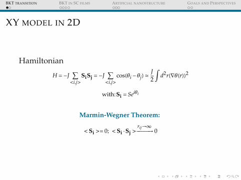
XY MODEL IN 2D
Hamiltonian
H =°JX
<i,j>S
i
S
j
=°JX
<i,j>cos(µi °µj) '
J2
Zd2r(rµ(r))2
with:Si
= Seiµi
Marmin-Wegner Theorem:
<S
i
>= 0; <S
i
·Sj
>rij!1°°°°°! 0

BKT TRANSITION BKT IN SC FILMS ARTIFICIAL NANOSTRUCTURE GOALS AND PERSPECTIVES
XY MODEL IN 2D
Hamiltonian
H =°JX
<i,j>S
i
S
j
=°JX
<i,j>cos(µi °µj) '
J2
Zd2r(rµ(r))2
with:Si
= Seiµi
Marmin-Wegner Theorem:
<S
i
>= 0; <S
i
·Sj
>rij!1°°°°°! 0
BUT:
8>><
>>:
T >TKT <S
i
·Sj
>ª e°|ri°rj|/ª
T <TKT <S
i
·Sj
>ª ( 1|ri°rj| )
T/2ºJ
BKT TRANSITION BKT IN SC FILMS ARTIFICIAL NANOSTRUCTURE GOALS AND PERSPECTIVES
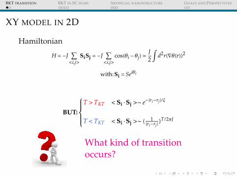
XY MODEL IN 2D
Hamiltonian
H =°JX
<i,j>S
i
S
j
=°JX
<i,j>cos(µi °µj) '
J2
Zd2r(rµ(r))2
with:Si
= Seiµi
BUT:
8>><
>>:
T >TKT <S
i
·Sj
>ª e°|ri°rj|/ª
T <TKT <S
i
·Sj
>ª ( 1|ri°rj| )
T/2ºJ
What kind of transitionoccurs?

BKT TRANSITION BKT IN SC FILMS ARTIFICIAL NANOSTRUCTURE GOALS AND PERSPECTIVES
THE ROLE OF VORTICESTHE GAUSSIAN APPROXIMATION IS NOT ENOUGH: IT DOESN’T TAKE INTO ACCOUNTTHE PRESENCE OF VORTICES!
Configurations such that:I
d2rrµ(r) = 2º

BKT TRANSITION BKT IN SC FILMS ARTIFICIAL NANOSTRUCTURE GOALS AND PERSPECTIVES
THE ROLE OF VORTICESTHE GAUSSIAN APPROXIMATION IS NOT ENOUGH: IT DOESN’T TAKE INTO ACCOUNTTHE PRESENCE OF VORTICES!
A simple estimate...
Entropic term
S= 2kB ln(La
)
Energetic term
E=ºJ ln(La
)
F=E°TS= (ºJ°2kBT) ln(La
)
TKT ' ºJ2kB
When does the transition occurs?
! Simple estimate: balance between energy and entropy
T<TBKT T>TBKT
Stuttgart, 13-01-2015

BKT TRANSITION BKT IN SC FILMS ARTIFICIAL NANOSTRUCTURE GOALS AND PERSPECTIVES
2D SUPERCONDUCTING FILMSWHERE IS THE CONNECTION WITH THE BKT TRANSITION?
HXY ª J2
Zd2r(rµ(r))2
S
i
= |S|eiµi
HS = 12
mns
Zd2rv2
s = fl2ns8m
Zd2r(rµ)2
™i = |¢|eiµi ; vS = fl2m
rµ
BKT TRANSITION BKT IN SC FILMS ARTIFICIAL NANOSTRUCTURE GOALS AND PERSPECTIVES
2D SUPERCONDUCTING FILMSWHERE IS THE CONNECTION WITH THE BKT TRANSITION?
HXY ª J2
Zd2r(rµ(r))2
S
i
= |S|eiµi
HS = 12
mns
Zd2rv2
s = fl2ns8m
Zd2r(rµ)2
™i = |¢|eiµi ; vS = fl2m
rµ
Superfluid Stiffness:
Js(TBKT) = fl2nsd4m
= fl2d4e2µo∏2 = 2TBKT
º
Js universal jump at T =TBKT is the hallmark of the transition!
BKT TRANSITION BKT IN SC FILMS ARTIFICIAL NANOSTRUCTURE GOALS AND PERSPECTIVES
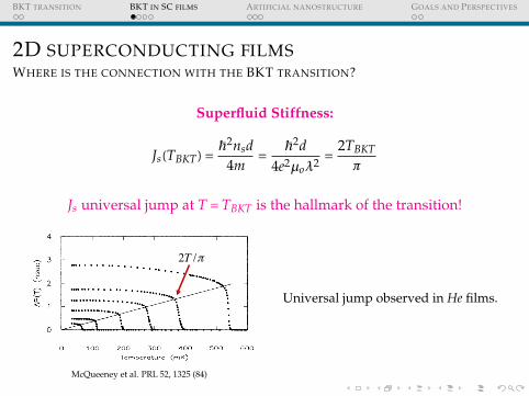
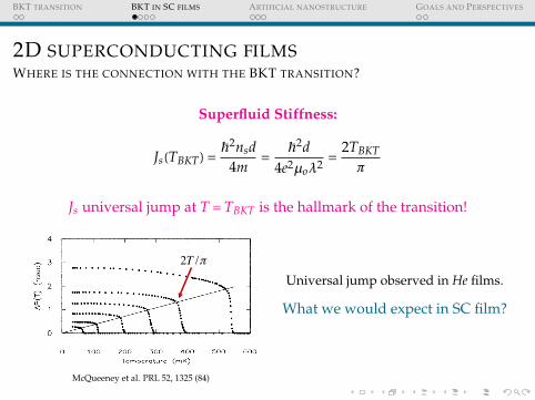
2D SUPERCONDUCTING FILMSWHERE IS THE CONNECTION WITH THE BKT TRANSITION?
Superfluid Stiffness:
Js(TBKT) = fl2nsd4m
= fl2d4e2µo∏2 = 2TBKT
º
Js universal jump at T =TBKT is the hallmark of the transition!
When does the transition occurs?
! Simple estimate: balance between energy and entropy
! This translates in the well known superfluid-density jump: at a critical value of the superfluid stiffness J the BKT transition occurs
Stuttgart, 13-01-2015
€
Js(TBKT ) =!2nsd4m
=!2d
4e2µ0λ2 =
2TBKTπ
He films McQueeney et al. PRL 52, 1325 (84)
€
2T /π
McQueeney et al. PRL 52, 1325 (84)
Universal jump observed in He films.
BKT TRANSITION BKT IN SC FILMS ARTIFICIAL NANOSTRUCTURE GOALS AND PERSPECTIVES
2D SUPERCONDUCTING FILMSWHERE IS THE CONNECTION WITH THE BKT TRANSITION?
Superfluid Stiffness:
Js(TBKT) = fl2nsd4m
= fl2d4e2µo∏2 = 2TBKT
º
Js universal jump at T =TBKT is the hallmark of the transition!
When does the transition occurs?
! Simple estimate: balance between energy and entropy
! This translates in the well known superfluid-density jump: at a critical value of the superfluid stiffness J the BKT transition occurs
Stuttgart, 13-01-2015
€
Js(TBKT ) =!2nsd4m
=!2d
4e2µ0λ2 =
2TBKTπ
He films McQueeney et al. PRL 52, 1325 (84)
€
2T /π
McQueeney et al. PRL 52, 1325 (84)
Universal jump observed in He films.
What we would expect in SC film?

BKT TRANSITION BKT IN SC FILMS ARTIFICIAL NANOSTRUCTURE GOALS AND PERSPECTIVES
BKT IN ULTRATHIN SC FILMSSOME COMPLICATIONS:
L. Presence of quasiparticles excitations
When does the transition occurs?
! Simple estimate: balance between energy and entropy
! This translates in the well known superfluid-density jump: at a critical value of the superfluid stiffness J the BKT transition occurs
Stuttgart, 13-01-2015
€
Js(TBKT ) =!2nsd4m
=!2d
4e2µ0λ2 =
2TBKTπ
However, additional effects are present that can modify this simple
text-book picture
L. Screening effects due to charged supercurrents©. Screening effects due to charged supercurrents
L. Presence of disorder
G.Lemarie et al PRB 87 (2013)
STM map of the localSC order parameter in
NbN-films

BKT TRANSITION BKT IN SC FILMS ARTIFICIAL NANOSTRUCTURE GOALS AND PERSPECTIVES
BKT IN ULTRATHIN SC FILMSSOME COMPLICATIONS:
L. Presence of quasiparticles excitations
L. Screening effects due to charged supercurrentsVortices interact logarithmically only up to the Pearl length
§= ∏2
d
©. Screening effects due to charged supercurrents
L. Presence of disorder
G.Lemarie et al PRB 87 (2013)
STM map of the localSC order parameter in
NbN-films

BKT TRANSITION BKT IN SC FILMS ARTIFICIAL NANOSTRUCTURE GOALS AND PERSPECTIVES
BKT IN ULTRATHIN SC FILMSSOME COMPLICATIONS:
L. Presence of quasiparticles excitations
L. Screening effects due to charged supercurrentsVortices interact logarithmically only up to the Pearl length
§= ∏2
d
Reducing the thickness d of the film !§> L) vortices interact logarithmically at all length scale!
©. Screening effects due to charged supercurrents
L. Presence of disorder
G.Lemarie et al PRB 87 (2013)
STM map of the localSC order parameter in
NbN-films

BKT TRANSITION BKT IN SC FILMS ARTIFICIAL NANOSTRUCTURE GOALS AND PERSPECTIVES
BKT IN ULTRATHIN SC FILMSSOME COMPLICATIONS:
L. Presence of quasiparticles excitations
L. Screening effects due to charged supercurrents
©. Screening effects due to charged supercurrents
L. Presence of disorder
i¿∝⟨Si⟩
G.Lemarie et al PRB 87 (2013)
STM map of the localSC order parameter in
NbN-films

BKT TRANSITION BKT IN SC FILMS ARTIFICIAL NANOSTRUCTURE GOALS AND PERSPECTIVES
DISORDERED ULTRATHIN SC FILMSTHEORETICAL STUDY:T.CEA, D. BUCHELI, G. SEIBOLD, L. BENFATTO, J. LORENZANA AND C. CASTELLANI PRB 89 (2014)
Mean Field calculations at T=0 for an effective boson model! Effective model with disordered coupling Jij
Jij = Jsin¡i sin¡jOPTICAL EXCITATION OF PHASE MODES IN STRONGLY . . . PHYSICAL REVIEW B 89, 174506 (2014)
0 5 10 150
0.04
0.08
0.12
N(ω
)
N(ω)
0 5 10 15ω/J, Eα/J
00.20.40.60.81
Z/J
Zα
0 10 20 30 40ω/J, Eα/J
0
0.04
0.08
0.12
N(ω
)
20 40 60 80 100Site i
-3-2-10123
φ α
20 40 60 80 100Site i
0
0.5
1
1.5
2
J ix /J
0 10 20 30 4000.20.40.60.81
Z/J
W/J=5.6 W/J=18 (b)
(c)E /J=0.26, Z /J<0.01
(a)
E /J=0.53, Z /J<0.01E /J=0.34, Z /J=0.35
E /J=0.35, Z /J=0.1
W/J=4
FIG. 5. (Color online) (a) and (b) Density of phase modes N (ω)and effective dipole Zα at two values of disorder (averaged over 100disorder configurations). (c) Spatial structure of the phase modesφαi in the one-dimensional case for a given disorder realization. Thesolid lines represent the spatial dependence of the eigenfunctions φαi
[whose gradient enters Eq. (17) for the effective dipole Zα] at selectedvalues of the excitation energies Eα . In the lower part of the figure wealso represent with bars the spatial variations of the local stiffness J x
i .As one can see, the largest effective dipole Zα is realized for the blueand orange excitations, whose monotonic phase variations overlapwith a region of large local stiffness.
σreg(ω) (see Appendix B). The results are shown in Fig. 3 and inthe inset of Fig. 2. As one can see, at large U the bosonic modelreproduces in a quantitative way the characteristic energyscales for optical absorption in the fermionic model. At weakercoupling the comparison is instead only qualitative, due partlyto the difficulties of clearly separating the contribution ofquasiparticles and collective modes.
Let us finally analyze the connection between the opticalresponse and the inhomogeneous spatial distribution of theSC properties. The optical response (16) is proportional tothe density of states of phase modes N (ω), weighted bythe effective dipole function Zα of Eq. (17). Both quantitiesdepend on disorder, as shown in Figs. 5(a) and 5(b), and ingeneral the 1/Eα prefactor of Eq. (17) favors a larger dipolefor lower-energy modes. In addition at strong disorder, whenthe system segregates into SC islands with large local stiffnessJ i
µ, the optical absorption is large when the phase excitationsoccur inside the SC regions, according to Eq. (17). This effectcan be better visualized in a one-dimensional version of themodel (10), as shown in Fig. 5(c). Here one can clearly see thatthe largest optical dipole is realized when a monotonic phasevariation overlaps with a good SC region. Since the charge isthe conjugate variable of the phase gradients, one then realizesa charge unbalance on the two sides of the island, making itoptically active.
At strong disorder this space-selective optical absorptionis strictly connected to the emergence of percolative pathsfor the superfluid currents, analogous to the ones discussedin Ref. [30] for the fermionic model (1). In Fig. 6 we showat two values of W/J the currents in the presence of a finiteapplied field A = −Ax for a given disorder configuration,superimposed on the map of the local stiffnesses J x
i . Since
W!J"10
5 10 15 20
5
10
15
20W!J"18
5 10 15 20
0.2 0.4 0.6 0.8 1Ji
x!J0
FIG. 6. (Color online) Local supercurrents (arrows) for an ap-plied field A = −Ax superimposed over the map of the localstiffnesses J x
i /J for a given disorder realization and two values ofW/J . The size of the arrows is proportional to the strength of thetotal local current, whose diamagnetic contribution is proportional tothe local stiffness displayed in the underlying map. The current flowsalong preferential paths connecting the regions with large J x
i . Thismeans that the isolated SC islands, i.e., those which reside far fromthe main percolative paths of the current, have a large paramagneticresponse responsible for the absorption at finite frequencies. Forexample, for W/J = 18 the whole diamagnetic contribution of thewhite regions on the bottom of the map is transferred to σreg(ω).
J xi is a measure of the local diamagnetic response, a small
current occurring over a good SC region is due to a large localparamagnetic response, i.e., to an optical absorption at finitefrequencies. At strong disorder the percolative supercurrentpaths leave aside several isolated SC islands, which thencontribute to σreg(ω) thanks to the dipole-activation mechanismexplained above.
IV. CONCLUSIONS
In summary, we computed the optical response due to col-lective modes in two prototype fermionic and bosonic modelsfor disordered superconductors. In both cases we find thatdisorder renders phase fluctuations optically active, in a rangeof energies that lies below the threshold for single-particleexcitations for the fermionic case. The bosonic approachallows us to establish a clear correspondence between theoptical response and the spatial inhomogeneity of the SC orderparameter, showing that optical absorption stems predomi-nantly from phase fluctuations within the good SC regions.Besides explaining recent experiments in strongly disorderedsuperconductors [14–17] our results could be further checkedexperimentally by means of near-field scanning microwaveimpedance microscopy [33]. Indeed, the proposed mechanismof direct correspondence between the SC granularity andoptical absorption, evidenced in Fig. 6, can be potentiallymapped out by this technique, which is able to resolve spatialvariations at length scales well below the radiation wavelength.In this respect the variation of the microwave optical propertiesof disordered superconductors at the nanoscale can be usedto improve the performance of SC microresonators built instandard geometries or even to design new nanoelectric devicestargeted for space- and frequency-selective applications.
174506-5
Disorder structured in real space!!

BKT TRANSITION BKT IN SC FILMS ARTIFICIAL NANOSTRUCTURE GOALS AND PERSPECTIVES
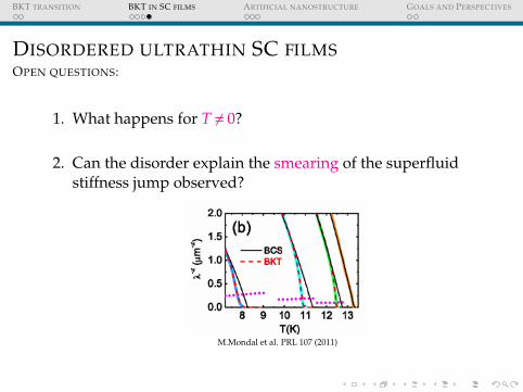
DISORDERED ULTRATHIN SC FILMSOPEN QUESTIONS:
1. What happens for T 6= 0?
2. Can the disorder explain the smearing of the superfluidstiffness jump observed?
M.Mondal et al. PRL 107 (2011)
BKT TRANSITION BKT IN SC FILMS ARTIFICIAL NANOSTRUCTURE GOALS AND PERSPECTIVES
DISORDERED ULTRATHIN SC FILMSOPEN QUESTIONS:
1. What happens for T 6= 0?
2. Can the disorder explain the smearing of the superfluidstiffness jump observed?
M.Mondal et al. PRL 107 (2011)

BKT TRANSITION BKT IN SC FILMS ARTIFICIAL NANOSTRUCTURE GOALS AND PERSPECTIVES
ARTIFICIAL NANOSTRUCTURE
œ Z.Han et al Nature 10 (2014)NATURE PHYSICS DOI: 10.1038/NPHYS2929 ARTICLES
b
a
cc
Vg
V
I
b
2a
1 µm5 µm
Figure 1 | Proximity-coupled array of superconducting discs on graphene.a, Schematics of the device, involving a triangular array of superconductingtin discs decorating the bare graphene surface. The device is connected to acurrent source and measured using a four-probe measurement set-up.b, Optical micrograph of the sample. The black lines indicate the graphenesample plasma-etched Hall bar, which is connected to the gold electrodesseen on the edge of the image. The graphene surface is decorated with aregular array of tin discs of diameter 400 nm, separated by 1 µm betweencentres. c, Scanning electron micrograph of the dashed rectangular regionin b showing the triangular lattice of tin discs with diameter 2a andseparated by a distance b.
superconductivity on the discs by the inverse proximity eect26.As we describe below, these capabilities, along with quantitativecomparisons with theory, allow us to reveal both the collapse ofsuperconductivity by quantum phase fluctuations, and the ensuing2D metallic state. In addition, under perpendicular magneticfield a re-entrant superconducting state is observed at our lowesttemperatures, as expected from theory27–29.
Berezinskii–Kosterlitz–Thouless transitionOur proximity-induced array consists of a triangular lattice ofdisc-shaped superconducting islands, which are deposited onto agraphene Hall bar equipped with a backgate electrode (Fig. 1). Thesuperconducting discs are in the form of 50 nm thick tin films, withdiameter 2a= 400 nm. Discs are separated by a distance b= 1µmbetween their centres (Fig. 1). The electronmobility of the grapheneextracted from a fit of the field eect and fromHall measurements is680 cm2 V1 s1 at high gate voltages (Supplementary Fig. 1), whilethe mean free path l can be varied with the backgate in the range10–30 nm (Supplementary Fig. 2), corresponding to a diusioncoecient D=50–140 cm2 s1 (Supplementary Fig. 2). Our systemdiers considerably from previous experiments performed on tin–graphene hybrids4,30, for which tin clusters of random shapesdensely self-assembled on the graphene surface by dewetting.Those experiments were performed in the opposite regime of shortjunctions (coherence length b) and in one case4 in the limitof strongly disordered graphene (mean free path b), for which
a superconductor-to-insulator quantum phase transition has beenobserved on decreasing the graphene charge carrier density.
We begin the presentation of the data by describing thetwo-step transition31,32 that the sample undergoes towards thesuperconducting state. On cooling from the normal state, a gate-independent resistance drop occurs at a temperature of ~3.6 K(Fig. 2a, red and blue curves, also Supplementary Fig. 3), whichis consistent with a previous observation of the superconductingtransition temperature of tin nanoparticles30. We attribute thisfirst drop to the superconducting transition of the discs, whichlocally shunt the graphene area underneath. The relative resistancedrop 1R/RN at this transition amounts to 20% on the electronside and 10% on the hole side, in good agreement with a modelincluding a carrier dependent tin/graphene interface transparency(Supplementary Information). Such an electron/hole asymmetry isrelated to the pinning of the charge density of graphene below themetal33, which in the case of tin30 leads to a p/n junction on thehole side and a transparent p/p junction on the electron side. In therest of the paper, we will focus rather on the electronic propertiesof the system on the electron side, for which the relative drop ofresistance 1R/RN exceeds the filling factor of the tin deposition(Supplementary Fig. 3), indicating that the tin/graphene interfaceconductance greatly exceeds the quantum of conductance.
Further cooling enhances the proximity eect via the graphene,which eventually leads to the percolation of superconductivity andthe establishment of a 2D superconducting state (SupplementaryFig. 3a,b). As shown in Fig. 2a, at gate voltages between 0 and 30V,the resistance decreases when the temperature is lowered from 3Kto 0.06K. An opposite trend is seen for gate voltages close to thecharge neutrality point (namely, from 30V to 0V).
Below 1K and for gate voltages above 3V, the proximity-coupled array develops full superconductivity, with a zeroresistance state and a gate-dependent critical temperature. Thetransition is captured by a Berezinskii–Kosterlitz–Thouless (BKT)mechanism34,35, which describes the 2D superconducting transitionas a proliferation and unbinding, atT BKT
c , of vortex–antivortex pairs,that is, thermal phase fluctuations of the superconducting orderparameter. A colour-scaled map showing the device resistanceversus gate voltage and temperature is shown in Fig. 2b. Theexperimentally measured superconducting temperature Tc isindicated by the white contour. The higher positive gate voltageleads to higher Tc, whereas Tc vanishes in the region around thecharge neutrality point, between 30V and 3V.
For Josephson junction arrays, the value of T BKTc is directly
proportional to the Josephson energy EJ(b,T ) of a single junctionformed between two superconducting discs. For a triangular lattice,the relation reads29:
T BKTc '1.47EJ(b,T BKT
c ) (1)
where EJ(b, T ) depends on the metal conductance g , the inter-disc distance b and the diusion coecient D (Methods). Usingexperimentally extracted values ofD and of the graphene resistancemeasured at 4 K for all back-gate values, we calculated T BKT
c bysolving (1) self-consistently with respect to T for the entire back-gate range (Methods). In Fig. 2b, the resulting T BKT
c is shown by thedashed line. For high gate voltages (that is,Vg >10V) this theoreticalvalue of T BKT
c is in excellent agreement with the experimentalcritical temperatureTc without any fitting parameter, supporting thetheoretical model29.
The critical supercurrent at T =0 provides another computablephysical quantity in such arrays. As shown in Fig. 3a, the plot ofthe dierential resistance dV/dI versus bias current and Vg allowsus to obtain the full Vg dependence on Ic at T = 0.06K. In thezero-temperature limit, the critical current of an array of discs canbe inferred from the Josephson coupling energy of neighbouring
NATURE PHYSICS | VOL 10 | MAY 2014 | www.nature.com/naturephysics 381
œ S.Eley et al Nature 4 (2011)
LETTERSPUBLISHED ONLINE: 4 DECEMBER 2011 | DOI: 10.1038/NPHYS2154
Approaching zero-temperature metallic statesin mesoscopic superconductor–normal–superconductor arraysSerena Eley1, Sarang Gopalakrishnan1, Paul M. Goldbart2 and Nadya Mason1*Systems of superconducting islands placed on normal metalfilms offer tunable realizations of two-dimensional (2D)superconductivity1,2; they can thus elucidate open questionsregarding the nature of 2D superconductors and competingstates. In particular, island systems have been predicted toexhibit zero-temperature metallic states3–5. Although evidenceexists for such metallic states in some 2D systems6,7, theircharacter is not well understood: the conventional theory ofmetals cannot explain them8, and their properties are dif-ficult to tune7,9. Here, we characterize the superconductingtransitions in mesoscopic island-array systems as a functionof island thickness and spacing. We observe two transitionsin the progression to superconductivity. Both transition tem-peratures exhibit unexpectedly strong depression for widelyspaced islands, consistent with the system approaching zero-temperature (T=0)metallic states. In particular, the first tran-sition temperature seems to linearly approach T = 0 for finiteisland spacing. The nature of the transitions is explained usinga phenomenological model involving the stabilization of super-conductivity on each island via a coupling to its neighbours.
Conventional zero-temperature (T = 0) metallic states do notexist in 2D systems possessing any disorder, because of Andersonlocalization8,9. To reconcile this fact with experimental evidence forT = 0 metals in 2D, it has been proposed that the experimentalobservations do not pertain to conventional metals, but ratherto spatially inhomogeneous superconducting (or, more generally,correlated) states3,4,10. Inhomogeneity is thought to arise in someof these systems because of phase separation; however, it can alsobe tunably engineered, for example, in hybrid superconductor–normal–superconductor (SNS) systems, such as the arrays studiedhere. In arrays of SNS junctions, the diffusion of electron pairsfrom the superconductor into the normal metal11–13—known as theproximity effect—gives rise to global superconductivity, through atransition typically described using the phenomenological theoryof Lobb, Abraham and Tinkham (LAT)14. According to the LATtheory, the T = 0 state is always superconducting, and no zero-temperature metallic state should appear.
Most previous studies of SNS arrays used islands much largerthan the superconducting coherence length SC (that is, havingwell-defined superconductivity)1; however, there is evidence thatarrays of mesoscopic islands (that is, islands of dimensionscomparable to SC) exhibit behaviour that deviates from theLAT theory5,15, and might therefore possess non-superconductingT = 0 states. Furthermore, the dependence of the superconductingtransition on key parameters—such as island spacing and size—has
1Department of Physics and Frederick Seitz Materials Research Laboratory, 104 South Goodwin Avenue, The University of Illinois Urbana-Champaign,Urbana, Illinois 61801-2902, USA, 2School of Physics, Georgia Institute of Technology, 837 State Street, Atlanta, Georgia 30332-0430, USA.*e-mail: [email protected].
c
a b
120 µm
I+I¬
v+ v¬
30 µ
m
Figure 1 |AFM topography of arrays of Nb islands on Au and SEM imageof device. a,b, AFM images of arrays of 87-nm-thick Nb islands (red) on10-nm-thick Au underlayer (yellow). Each array has an edge-to-edgespacing of 140 nm (a) and 340 nm (b). The scale bar is 500 nm. c, Falsecolour SEM image of island array (red rectangle) overlapping Au four-probepattern (yellow), with the measurement schematic indicated.
not previously been studied systematically. In this Letter, we presenttransport measurements on arrays of mesoscopic niobium (Nb)islands having systematically varying inter-island spacings, placedon patterned gold (Au) films. We observe that the device resistancedrops to zero in two steps as the temperature is lowered. The lower-temperature drop, at temperature T2, is associated with super-conducting phase-locking across the array; the data show that thedependence of T2 on island spacing and thickness deviates stronglyfrom LAT theory. Surprisingly, the higher-temperature drop, at T1,traditionally associated with the superconducting transition of eachisland, also depends strongly on the island spacing, and seems toextrapolate to zero at finite spacings. This observation implies thatsuperconductivity on individual islands is fragile, and that a T = 0metallic statemight be realizable for veryweakly coupled islands.
Our samples consist of 10 nm-thick Au, patterned for four-pointtransport measurements, on Si/SiO2 substrates (see Methods forfabrication details). The Au patterns are overlaid with triangulararrays of 260 nm diameter Nb islands, as shown in Fig. 1. Eacharray contains more than 10,000 Nb islands. The data in this Letterare from two sets of devices: having 87-nm (±2 nm)- and 145-nm(±2 nm)-thick Nb islands respectively. The devices in each setare identical, except for varied island spacing. X-ray diffractionand scanning electron microscopy of the Nb revealed columnargrains30 nm in diameter, typical of evaporated Nb (ref. 16); thus,
NATURE PHYSICS | VOL 8 | JANUARY 2012 | www.nature.com/naturephysics 59

BKT TRANSITION BKT IN SC FILMS ARTIFICIAL NANOSTRUCTURE GOALS AND PERSPECTIVES
HYBRID TIN°GRAPHENE JOSEPHSON JUNCTIONARRAYZ.HAN ET AL NATURE 10 (2014)
NATURE PHYSICS DOI: 10.1038/NPHYS2929 ARTICLES
b
a
cc
Vg
V
I
b
2a
1 µm5 µm
Figure 1 | Proximity-coupled array of superconducting discs on graphene.a, Schematics of the device, involving a triangular array of superconductingtin discs decorating the bare graphene surface. The device is connected to acurrent source and measured using a four-probe measurement set-up.b, Optical micrograph of the sample. The black lines indicate the graphenesample plasma-etched Hall bar, which is connected to the gold electrodesseen on the edge of the image. The graphene surface is decorated with aregular array of tin discs of diameter 400 nm, separated by 1 µm betweencentres. c, Scanning electron micrograph of the dashed rectangular regionin b showing the triangular lattice of tin discs with diameter 2a andseparated by a distance b.
superconductivity on the discs by the inverse proximity eect26.As we describe below, these capabilities, along with quantitativecomparisons with theory, allow us to reveal both the collapse ofsuperconductivity by quantum phase fluctuations, and the ensuing2D metallic state. In addition, under perpendicular magneticfield a re-entrant superconducting state is observed at our lowesttemperatures, as expected from theory27–29.
Berezinskii–Kosterlitz–Thouless transitionOur proximity-induced array consists of a triangular lattice ofdisc-shaped superconducting islands, which are deposited onto agraphene Hall bar equipped with a backgate electrode (Fig. 1). Thesuperconducting discs are in the form of 50 nm thick tin films, withdiameter 2a= 400 nm. Discs are separated by a distance b= 1µmbetween their centres (Fig. 1). The electronmobility of the grapheneextracted from a fit of the field eect and fromHall measurements is680 cm2 V1 s1 at high gate voltages (Supplementary Fig. 1), whilethe mean free path l can be varied with the backgate in the range10–30 nm (Supplementary Fig. 2), corresponding to a diusioncoecient D=50–140 cm2 s1 (Supplementary Fig. 2). Our systemdiers considerably from previous experiments performed on tin–graphene hybrids4,30, for which tin clusters of random shapesdensely self-assembled on the graphene surface by dewetting.Those experiments were performed in the opposite regime of shortjunctions (coherence length b) and in one case4 in the limitof strongly disordered graphene (mean free path b), for which
a superconductor-to-insulator quantum phase transition has beenobserved on decreasing the graphene charge carrier density.
We begin the presentation of the data by describing thetwo-step transition31,32 that the sample undergoes towards thesuperconducting state. On cooling from the normal state, a gate-independent resistance drop occurs at a temperature of ~3.6 K(Fig. 2a, red and blue curves, also Supplementary Fig. 3), whichis consistent with a previous observation of the superconductingtransition temperature of tin nanoparticles30. We attribute thisfirst drop to the superconducting transition of the discs, whichlocally shunt the graphene area underneath. The relative resistancedrop 1R/RN at this transition amounts to 20% on the electronside and 10% on the hole side, in good agreement with a modelincluding a carrier dependent tin/graphene interface transparency(Supplementary Information). Such an electron/hole asymmetry isrelated to the pinning of the charge density of graphene below themetal33, which in the case of tin30 leads to a p/n junction on thehole side and a transparent p/p junction on the electron side. In therest of the paper, we will focus rather on the electronic propertiesof the system on the electron side, for which the relative drop ofresistance 1R/RN exceeds the filling factor of the tin deposition(Supplementary Fig. 3), indicating that the tin/graphene interfaceconductance greatly exceeds the quantum of conductance.
Further cooling enhances the proximity eect via the graphene,which eventually leads to the percolation of superconductivity andthe establishment of a 2D superconducting state (SupplementaryFig. 3a,b). As shown in Fig. 2a, at gate voltages between 0 and 30V,the resistance decreases when the temperature is lowered from 3Kto 0.06K. An opposite trend is seen for gate voltages close to thecharge neutrality point (namely, from 30V to 0V).
Below 1K and for gate voltages above 3V, the proximity-coupled array develops full superconductivity, with a zeroresistance state and a gate-dependent critical temperature. Thetransition is captured by a Berezinskii–Kosterlitz–Thouless (BKT)mechanism34,35, which describes the 2D superconducting transitionas a proliferation and unbinding, atT BKT
c , of vortex–antivortex pairs,that is, thermal phase fluctuations of the superconducting orderparameter. A colour-scaled map showing the device resistanceversus gate voltage and temperature is shown in Fig. 2b. Theexperimentally measured superconducting temperature Tc isindicated by the white contour. The higher positive gate voltageleads to higher Tc, whereas Tc vanishes in the region around thecharge neutrality point, between 30V and 3V.
For Josephson junction arrays, the value of T BKTc is directly
proportional to the Josephson energy EJ(b,T ) of a single junctionformed between two superconducting discs. For a triangular lattice,the relation reads29:
T BKTc '1.47EJ(b,T BKT
c ) (1)
where EJ(b, T ) depends on the metal conductance g , the inter-disc distance b and the diusion coecient D (Methods). Usingexperimentally extracted values ofD and of the graphene resistancemeasured at 4 K for all back-gate values, we calculated T BKT
c bysolving (1) self-consistently with respect to T for the entire back-gate range (Methods). In Fig. 2b, the resulting T BKT
c is shown by thedashed line. For high gate voltages (that is,Vg >10V) this theoreticalvalue of T BKT
c is in excellent agreement with the experimentalcritical temperatureTc without any fitting parameter, supporting thetheoretical model29.
The critical supercurrent at T =0 provides another computablephysical quantity in such arrays. As shown in Fig. 3a, the plot ofthe dierential resistance dV/dI versus bias current and Vg allowsus to obtain the full Vg dependence on Ic at T = 0.06K. In thezero-temperature limit, the critical current of an array of discs canbe inferred from the Josephson coupling energy of neighbouring
NATURE PHYSICS | VOL 10 | MAY 2014 | www.nature.com/naturephysics 381
S.Eleyet al Nature 4 (2011)
The gate-tunable sheet resistanceof graphene allows to vary the
coupling J between islands.
Collapse of superconductivity at T = 0.! Emergence of an unexpected state.
ARTICLES NATURE PHYSICS DOI: 10.1038/NPHYS2929
5
4
3
2
1
0
dV
/dI (
h/4e
2 )
20 30100−10−20
60 mK3 K4 K
a
Vd
b
Gate voltage (V)
0.1
1.0
−30 −20 −10 0 10 20 30
S
10
60
1.0
0.1
Gate voltage (V)
Tem
pera
ture
(K)
(kΩ)
c
101
102
103
104
Res
istan
ce (Ω
)
0.1 1.0 4.0Temperature (K)
Vg−Vd (V)035791318233343
Figure 2 | Collapse of superconductivity in the proximity-coupled array. a, Gate voltage dependence of the four-probe resistance for three dierenttemperatures. The curve at T = 4 K gives the gate dependence of the device resistance above the superconducting transition of the tin discs. At T =3 K, theresistance drops throughout the full gate range owing to the superconducting transition of the tin discs. At the base temperature of 0.06 K, the arrayundergoes a transition from the superconducting to the resistive state for 29 V <Vg <3 V and the resistance exhibits a sharp peak at the chargeneutrality point, indicated by Vd, the so-called Dirac voltage. b, Colour-scaled map of resistance versus temperature and gate voltage ( Vg). Thesuperconducting phase (S) on the electron-doped side is shown as the blue area and the superconducting critical temperature Tc bordering the resistivestate is indicated by the white contour. The dashed line is calculated from equation (1) without a fitting parameter. The experimental Tc deviates aroundVg =5 V towards a sharp breakdown of the superconducting state at Vg =3 V. c, Line cuts from b of the temperature dependence of the array resistance.Whereas the resistance drops into a fully superconducting state for Vg Vd > 10V, a levelling-o to a gate-dependent finite value is observed for0<Vg Vd < 10V.
discs29, which is given by:
EJ (b,T =0)= 3
4gD
b2 ln2(b/a)=
2eI1 (2)
where g =/(e2R) is the dimensionless conductance of graphenein the normal state, with R the sheet resistance, and I1 is themaximum supercurrent between two neighbouring discs. The totalcritical current Ic can be estimated by summing the local criticalcurrent I1 of each of the disc neighbours (Fig. 1b) of the array,which contribute as parallel channels, and by neglecting the smallcontribution to Ic fromnon-nearest pairs of discs, leading to: Ic 6I1.According to the above relations, at T Tc, the product of IcRN(RN being the graphene sheet resistance in the normal state) shoulddepend only on diusion coecient D for a given geometry. Thiscan be directly tested, as the use of graphene as a 2D disorderedmetal enables one to gate-tune the diusion coecient whilekeeping all geometrical aspects of the array constant. By extractingthe experimental critical current Ic from Fig. 3a, and measuring RNat 4 K (Fig. 2a), we plot the quantity eIcRN/D as a function of thegate voltage in Fig. 3b. One can see that above a given doping level
this quantity reaches a constant level of 3.6×109cm2. Such a valuematches the quantity 33/b2 ln2(b/a) (dashed line in Fig. 3b), whichdepends only on the geometry of the array. Therefore, at high gatevoltages, this experiment follows the theoretical predictions for suchproximity-coupled arrays of discs sparsely decorating graphene29.
Quantum breakdown of superconductivityThe central result of this work is the anomalous reduction of thesample’s critical temperature Tc with respect to the calculated TBKTon increasing graphene resistance, leading to a sudden collapse ofsuperconductivity when approaching the charge neutrality point ofthe graphene layer (dark red region of Fig. 2b). The Vg-dependenceof Tc shown in Fig. 2b first deviates from T BKT
c towards lowertemperatures for Vg < 10 V, and then abruptly drops to zero ataround3V. The suppression of superconductivity is also apparentin the Vg-dependence of the critical supercurrent Ic at 0.06 K. Ascan be seen in Fig. 3, the zero-resistance state (blue region, markedas ‘S’ in Fig. 3a) disappears when Vg = 3V, in a similar fashionas for Tc. We attribute these significant deviations, culminatingin the collapse of superconductivity, to the failure of the BKTmodel29, which takes into account only thermal phase fluctuations.
382 NATURE PHYSICS | VOL 10 | MAY 2014 | www.nature.com/naturephysics
BKT TRANSITION BKT IN SC FILMS ARTIFICIAL NANOSTRUCTURE GOALS AND PERSPECTIVES
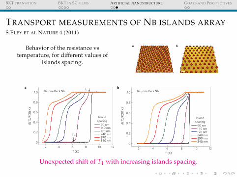
TRANSPORT MEASUREMENTS OF NB ISLANDS ARRAYS.ELEY ET AL NATURE 4 (2011)
Behavior of the resistance vstemperature, for different values of
islands spacing.
LETTERSPUBLISHED ONLINE: 4 DECEMBER 2011 | DOI: 10.1038/NPHYS2154
Approaching zero-temperature metallic statesin mesoscopic superconductor–normal–superconductor arraysSerena Eley1, Sarang Gopalakrishnan1, Paul M. Goldbart2 and Nadya Mason1*Systems of superconducting islands placed on normal metalfilms offer tunable realizations of two-dimensional (2D)superconductivity1,2; they can thus elucidate open questionsregarding the nature of 2D superconductors and competingstates. In particular, island systems have been predicted toexhibit zero-temperature metallic states3–5. Although evidenceexists for such metallic states in some 2D systems6,7, theircharacter is not well understood: the conventional theory ofmetals cannot explain them8, and their properties are dif-ficult to tune7,9. Here, we characterize the superconductingtransitions in mesoscopic island-array systems as a functionof island thickness and spacing. We observe two transitionsin the progression to superconductivity. Both transition tem-peratures exhibit unexpectedly strong depression for widelyspaced islands, consistent with the system approaching zero-temperature (T=0)metallic states. In particular, the first tran-sition temperature seems to linearly approach T = 0 for finiteisland spacing. The nature of the transitions is explained usinga phenomenological model involving the stabilization of super-conductivity on each island via a coupling to its neighbours.
Conventional zero-temperature (T = 0) metallic states do notexist in 2D systems possessing any disorder, because of Andersonlocalization8,9. To reconcile this fact with experimental evidence forT = 0 metals in 2D, it has been proposed that the experimentalobservations do not pertain to conventional metals, but ratherto spatially inhomogeneous superconducting (or, more generally,correlated) states3,4,10. Inhomogeneity is thought to arise in someof these systems because of phase separation; however, it can alsobe tunably engineered, for example, in hybrid superconductor–normal–superconductor (SNS) systems, such as the arrays studiedhere. In arrays of SNS junctions, the diffusion of electron pairsfrom the superconductor into the normal metal11–13—known as theproximity effect—gives rise to global superconductivity, through atransition typically described using the phenomenological theoryof Lobb, Abraham and Tinkham (LAT)14. According to the LATtheory, the T = 0 state is always superconducting, and no zero-temperature metallic state should appear.
Most previous studies of SNS arrays used islands much largerthan the superconducting coherence length SC (that is, havingwell-defined superconductivity)1; however, there is evidence thatarrays of mesoscopic islands (that is, islands of dimensionscomparable to SC) exhibit behaviour that deviates from theLAT theory5,15, and might therefore possess non-superconductingT = 0 states. Furthermore, the dependence of the superconductingtransition on key parameters—such as island spacing and size—has
1Department of Physics and Frederick Seitz Materials Research Laboratory, 104 South Goodwin Avenue, The University of Illinois Urbana-Champaign,Urbana, Illinois 61801-2902, USA, 2School of Physics, Georgia Institute of Technology, 837 State Street, Atlanta, Georgia 30332-0430, USA.*e-mail: [email protected].
c
a b
120 µm
I+I¬
v+ v¬
30 µ
m
Figure 1 |AFM topography of arrays of Nb islands on Au and SEM imageof device. a,b, AFM images of arrays of 87-nm-thick Nb islands (red) on10-nm-thick Au underlayer (yellow). Each array has an edge-to-edgespacing of 140 nm (a) and 340 nm (b). The scale bar is 500 nm. c, Falsecolour SEM image of island array (red rectangle) overlapping Au four-probepattern (yellow), with the measurement schematic indicated.
not previously been studied systematically. In this Letter, we presenttransport measurements on arrays of mesoscopic niobium (Nb)islands having systematically varying inter-island spacings, placedon patterned gold (Au) films. We observe that the device resistancedrops to zero in two steps as the temperature is lowered. The lower-temperature drop, at temperature T2, is associated with super-conducting phase-locking across the array; the data show that thedependence of T2 on island spacing and thickness deviates stronglyfrom LAT theory. Surprisingly, the higher-temperature drop, at T1,traditionally associated with the superconducting transition of eachisland, also depends strongly on the island spacing, and seems toextrapolate to zero at finite spacings. This observation implies thatsuperconductivity on individual islands is fragile, and that a T = 0metallic statemight be realizable for veryweakly coupled islands.
Our samples consist of 10 nm-thick Au, patterned for four-pointtransport measurements, on Si/SiO2 substrates (see Methods forfabrication details). The Au patterns are overlaid with triangulararrays of 260 nm diameter Nb islands, as shown in Fig. 1. Eacharray contains more than 10,000 Nb islands. The data in this Letterare from two sets of devices: having 87-nm (±2 nm)- and 145-nm(±2 nm)-thick Nb islands respectively. The devices in each setare identical, except for varied island spacing. X-ray diffractionand scanning electron microscopy of the Nb revealed columnargrains30 nm in diameter, typical of evaporated Nb (ref. 16); thus,
NATURE PHYSICS | VOL 8 | JANUARY 2012 | www.nature.com/naturephysics 59
LETTERS NATURE PHYSICS DOI: 10.1038/NPHYS2154
a
c
Island
R(T)
/R(1
0 K
)
T (K)
Islandspacing
Islandspacing
T1
T2
87-nm-thick Nb
Coherent islands:superconducting state
Resi
stan
ce
T2
J′ kBT>∼ Coherent grains
JJ′Supercond.
phase
Normal state
Grain
T1
Temperature
J (kBT)2/J′>∼
0
0.2
0.4
0.6
0.8
1.0
2 4 6 8 10 12
90 nm140 nm190 nm240 nm290 nm340 nm
b
R(T)
/R(1
0 K
)
T (K)
145-nm-thick Nb
0
0.2
0.4
0.6
0.8
1.0
2 4 6 8 10 12
90 nm140 nm190 nm240 nm290 nm340 nm
V IV III II I
Figure 2 | Superconductivity in Nb island arrays. a,b, Temperature dependent resistive transitions in arrays having different edge-to-edge island spacings.The island diameter is 260 nm for all arrays. The islands are 87 nm thick (a) and 145 nm thick (b). Black arrows in a mark T1 and T2 for the islands spaced140 nm apart. The data are normalized to the resistance at 10 K. Note that T1 and T2 occur at higher temperatures for thicker islands. In a, the lowesttemperature curves are cut off by the minimum attainable temperature of our apparatus. c, The curve illustrates two-step resistance versus temperaturebehaviour, with the island transition marked at T1, and film transition marked at T2. Pictures show three islands, each limited to four grains for simplicity. Inregion I, the Nb islands are normal metals. In region II, the phase of the grains (represented by arrows) starts to become coherent throughout each island(although there is not yet inter-island phase coherence). At T1, Cooper pairs diffuse from the Nb into the Au, and the resistance drops. The grains haveintra-island Josephson coupling J and nearest-neighbour inter-island coupling J’(represented by red squiggly lines). In region III, J has saturated, but J’continues to increase as the normal metal coherence length N increases. In region IV, N becomes comparable to the island spacing, and the entire systemof film and islands progresses towards having global phase coherence. As the temperature is further decreased, the film undergoes a transition to asuperconducting state at T2.
each Nb island contains 50–100 grains. The superconductingcoherence length of Nb is estimated to be 27 nm (see Methods),comparable to the grain size but smaller than the island size.
Figure 2 shows resistance measurements for the devices, as wellas an illustration of the two-step development of superconductivity.The data in Fig. 2a,b show that both T1 and T2 decrease withincreasing island spacing. The resistance exhibits an abrupt changein slope at T1, but not the sharp drop seen for larger islands1.Figure 3 shows a plot of T1 versus island spacing. It is evident thatT1 decreases more rapidly for the shorter islands, but seems todecrease linearly with spacing for both the shorter and taller islands,extrapolating to zero at840 nm and2,600 nm, respectively. TheresultingT =0 states would thus bemetallic in that they would havefinite resistance at finite island spacing. The data in Fig. 2 also showthat T2 is more strongly depressed for shorter islands than for tallerislands. As schematized in Fig. 2c, these trends can be understoodusing a model of coupled islands, each composed of grains, havingtwo characteristic energy scales: (1) J , the coupling between grainson an individual island, and (2) J 0 (<J ), the coupling between grainson neighbouring islands. According to this scheme, for T >T1, theseparate grains on each island have incoherent superconductingphases; at T1, intra-island phase coherence develops, and thesystem’s resistance decreases. For very large islands, T1 woulddepend only on J , which grows with island height but is spacing-independent. Formesoscopic islands, however, the T1 of an isolatedisland is depressed (possibly to T = 0) by phase fluctuationsamong the grains; the inter-island coupling J 0 serves to reduce
these fluctuations by increasing the effective ‘dimensionality’ ofthe island system, thereby stabilizing superconductivity. Thus, T1decreases for larger spacings (that is, as J 0 decreases). Below T1,the intra-island phase coherence strengthens continuously (Fig. 2c,region II); thus, the system resistance continuously decreases ratherthan steeply dropping at T1. Region III of Fig. 2c shows the familiarproximity behaviour; here, the normal-metal coherence length17 Nincreases until it becomes comparable to the island spacing. Then,inter-island phase coherence begins to emerge (Fig. 2c, region IV),and at T2 the system undergoes a Berezinskii–Kosterlitz–Thoulesstransition to a fully superconducting state1,2.
The inset to Fig. 4 shows how T2 decreases with increasingisland spacing. For each device, T2 was extracted by measuringthe temperature at which current–voltage (I–V ) curves becamenonlinear (see Supplementary Information). The dependence of T2on array parameters deviates from LAT theory both quantitatively(that is, T2 decreases more rapidly with island spacing thanpredicted) and qualitatively (that is, T2 depends strongly on islandheight). Figure 4 also shows the systematic dependence of N(T2)on island spacing, where N = p
hD/(kBT ) and the normal-metaldiffusion constant D 94 cm2 s1 (see Methods). We observeN(T2) to vary approximately linearly with island spacing.
We now turn to a more quantitative description of thesetransitions. From the Ginzburg–Landau perspective, T1 for anisolated island of lateral dimensions comparable to SC shouldequal the transition temperature for a continuous film of thesame height, because the suppression of superconductivity due to
60 NATURE PHYSICS | VOL 8 | JANUARY 2012 | www.nature.com/naturephysics
Unexpected shift of T1 with increasing islands spacing.
BKT TRANSITION BKT IN SC FILMS ARTIFICIAL NANOSTRUCTURE GOALS AND PERSPECTIVES
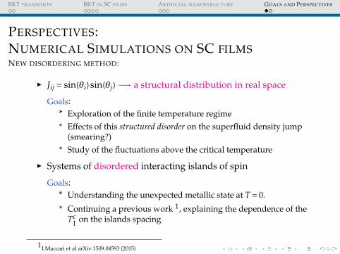
PERSPECTIVES:NUMERICAL SIMULATIONS ON SC FILMSNEW DISORDERING METHOD:
œ Jij = sin(µi)sin(µj) °! a structural distribution in real space
Goals:* Exploration of the finite temperature regime* Effects of this structured disorder on the superfluid density jump
(smearing?)* Study of the fluctuations above the critical temperature
œ Systems of disordered interacting islands of spin
Goals:* Understanding the unexpected metallic state at T = 0.
* Continuing a previous work 1, explaining the dependence of theTc
1 on the islands spacing
1I.Maccari et al arXiv:1509.04593 (2015)

BKT TRANSITION BKT IN SC FILMS ARTIFICIAL NANOSTRUCTURE GOALS AND PERSPECTIVES
Thank you for yourattention!