bismuth – based oxide semiconductors: mild synthesi s …
TRANSCRIPT

BISMUTH – BASED OXIDE SEMICONDUCTORS: MILD SYNTHESIS
AND PRACTICAL APPLICATIONS
by
HARI KRISHNA TIMMAJI
Presented to the Faculty of the Graduate School of
The University of Texas at Arlington in Partial Fulfillment
of the Requirements
for the Degree of
DOCTOR OF PHILOSOPHY
THE UNIVERSITY OF TEXAS AT ARLINGTON
December 2011

Copyright © by Hari Krishna Timmaji 2011
All Rights Reserved

iii
ACKNOWLEDGEMENTS
With great pleasure and gratitude, I express my sincere thanks to my research advisor
Professor Krishnan Rajeshwar for his continuous guidance and encouragement throughout my
research work.
I extend my sincere thanks and gratitude to my committee members, Professors
Purnendu (Sandy) Dasgupta, James Grover, Melanie Sattler, and Richard (Xiyun) Guan for their
valuable guidance and advice.
My special thanks go to Professor Norma Tacconi for her immense patience with me,
moral support, help, and valuable discussions throughout my research. I also thank all the past
and present members of our research group for their contributions to my research.
I especially thank my parents Sri. Vedanta Chary and Smt. Anooradha, my sister Bindu,
my brother-in-law Krishna, and my niece Laasya, for providing me their unending support and
encouragement throughout my career and life. I thank Dr. Devi Majumdar, for her suggestions in
writing this dissertation, her constant support, and trust in me. I also acknowledge my friends,
Srinivas Prabakar and Karthik Shastry, for being great roommates and for sharing my ups and
downs during my time at UTA.
Finally, I thank the Department of Earth & Environmental Sciences, and the Department
of Chemistry, at University of Texas at Arlington, for giving me an opportunity to follow my dream
and for extending financial support for this dissertation study.
October 17, 2011

iv
ABSTRACT
BISMUTH – BASED OXIDE SEMICONDUCTORS: MILD SYNTHESIS
AND PRACTICAL APPLICATIONS
Hari Krishna Timmaji, PhD
The University of Texas at Arlington, 2011
Supervising Professor: Krishnan Rajeshwar
In this dissertation study, bismuth based oxide semiconductors were prepared using
‘mild’ synthesis techniques – electrodepostion and solution combustion synthesis. Potential
environmental remediation and solar energy applications of the prepared oxides were evaluated.
Bismuth vanadate (BiVO4) was prepared by electrodeposition and solution combustion
synthesis. A two step electrosynthesis strategy was developed and demonstrated for the first
time. In the first step, a Bi film was first electrodeposited on a Pt substrate from an acidic BiCl3
medium. Then, this film was anodically stripped in a medium containing hydrolyzed vanadium
precursor, to generate Bi3+, and subsequent BiVO4 formation by in situ precipitation. The
photoelectrochemical data were consistent with the in situ formation of n-type semiconductor
films.

v
In the solution combustion synthesis procedure, BiVO4 powders were prepared using
bismuth nitrate pentahydrate as the bismuth precursor and either vanadium chloride or vanadium
oxysulfate as the vanadium precursor. Urea, glycine, or citric acid was used as the fuel. The
effect of the vanadium precursor on the photocatalytic activity of combustion synthesized BiVO4
was evaluated in this study. Methyl orange was used as a probe to test the photocatalytic
attributes of the combustion synthesized (CS) samples, and benchmarked against a commercial
bismuth vanadate sample. The CS samples showed superior activity to the commercial
benchmark sample, and samples derived from vanadium chloride were superior to vanadium
oxysulfate counterparts. The photoelectrochemical properties of the various CS samples were
also studied and these samples were shown to be useful both for environmental photocatalytic
remediation and water photooxidation applications.
Silver bismuth tungstate (AgBiW2O8) nanoparticles were prepared for the first time by
solution combustion synthesis by using silver nitrate, bismuth nitrate, sodium tungstate as
precursors for Ag, Bi, and W respectively and urea as the fuel. The photocatalytic activity of
these nanoparticles was superior to a sample prepared by solid-state synthesis. The
combustion-synthesized particles were subsequently modified with Pt catalyst islands using a
photodepostion technique and then used for the photo-generation of syngas (CO + H2). Formic
acid was used in these experiments for in situ generation of CO2 and its subsequent reduction to
CO. In the absence of Pt modification, H2 was not obtained. These results were compared with
those obtained with acetic acid in place of formic acid, and finally the mechanistic pathways for
syngas and methane photogeneration are presented.

vi
TABLE OF CONTENTS
ACKNOWLEDGEMENTS ................................................................................................................ iii ABSTRACT ...................................................................................................................................... iv LIST OF ILLUSTRATIONS .............................................................................................................. ix LIST OF TABLES ........................................................................................................................... xii Chapter Page
1. INTRODUCTION……………………………………..………..….. ...................................... 1
1.1 Oxide Semiconductors ..................................................................................... 1
1.1.1 Electronic Band Structure of Solids .................................................. 3
1.1.2 Photocatalysis .................................................................................. 4
1.2 Energy Payback Time and Mild Synthesis of Inorganic Semiconductors ....... 8
1.3 Electrodeposition of Inorganic Oxide Semiconductors ..................................... 9
1.3.1 Photoelectrochemical Concepts ..................................................... 12
1.4 Combustion Synthesis of Oxide Semiconductors .......................................... 16 1.5 Oxide Semiconductors and Photocatalysis .................................................... 19
1.5.1 Bismuth Vanadate (BiVO4) ............................................................. 19
1.5.2 Silver Bismuth Tungstate (AgBiW2O8)............................................ 23
2. EXPERIMENTAL .......................................................................................................... 26
2.1 Bismuth Vanadate (BiVO4) ............................................................................. 26
2.1.1 Solution Combustion Synthesis of BiVO4 ....................................... 26
vii
2.2 Silver Bismuth Tungstate (AgBiW2O8) ............................................................ 27
2.2.1 Solution Combustion Synthesis of AgBiW2O8 ................................ 28 2.2.2 Platinum (Pt) Photodeposition on SCS–AgBiW2O8 ........................ 28
2.3 Sample Characterization ................................................................................ 29 2.3.1 Thermogravimetric Analysis (TGA) ................................................ 29
2.3.2 Differential Scanning Calorimetry (DSC) ........................................ 29
2.3.3 X – Ray Diffraction (XRD) .............................................................. 30 2.3.4 Diffuse Reflectance Spectroscopy (DFR) ...................................... 31 2.3.5 X – Ray Photoelectron Spectroscopy (XPS) .................................. 32 2.3.6 Raman Spectroscopy ..................................................................... 32
2.4 Photocatalysis Experiments ........................................................................... 33 2.5 DFT Methodology ........................................................................................... 36 2.6 Photoelectrochemistry .................................................................................... 36
2.7 Electrosynthesis of BiVO4 Electrodes ............................................................ 37
3. RESULTS AND DISCUSSION ..................................................................................... 39
3.1 Solution Combustion Synthesis of BiVO4 ....................................................... 39
3.1.1 Fuel Precursor Combinations and Thermal Analyses .................... 39
3.1.2 Influence of Vanadium Precursor ................................................... 42 3.1.3 Sample Characterization ................................................................ 43
3.2 Photocatalytic Behavior of BiVO4 ................................................................... 52 3.3 Photoelectrochemistry of BiVO4 ..................................................................... 57 3.4 Electrosynthesis of BiVO4 ............................................................................... 61
3.4.1 Optimization and Miscellaneous Aspects ....................................... 61 3.4.2 Sample Characterization ................................................................ 62
3.5 Photoelectrochemical Behavior ...................................................................... 66

viii
3.6 Solution Combustion Synthesis of AgBiW2O8 ................................................ 68
3.6.1 Crystal Structure Modeling Considerations .................................... 68 3.6.2 Electronic Structure Calculations ................................................... 70 3.6.3 Sample Characterization ................................................................ 73
3.7 Photocatalytic Behavior of AgBiW2O8 ............................................................ 79
3.7.1 Photodegradation of Methyl Orange .............................................. 79
3.7.2 Photogeneration of Syngas (CO + H2) and Methane on Pt – modified AgBiW2O8 ............................................................ 82
4. SUMMARY AND CONCLUSIONS ............................................................................... 90
REFERENCES ............................................................................................................................... 92 BIOGRAPHICAL INFORMATION ................................................................................................ 100

ix
LIST OF ILLUSTRATIONS
Figure Page 1.1 Spectral distribution of solar photon flux .................................................................................... 2 1.2 Electronic energy structure for solids ......................................................................................... 3 1.3 Schematic diagram of photocatalysis on the semiconductor particle ........................................ 5 1.4 Schematic representation of the recombination and redox processes on the semiconductor particle. 1 = charge carrier generation; 2 = bulk recombination; 3 = surface recombination; 4 = charge transfer .................................. 6 1.5 Band edge positions of semiconductors ..................................................................................... 8 1.6 Representation of (a) n – type and (b) p – type semiconductors. EC is the conduction band energy level, EV is the valence band energy level, EF is the Fermi level of the semiconductor, ED and EA are the energy levels created by the donor and acceptor dopants, respectively. ...................................................... 13 1.7 Band bending for (a) n – type and (b) p – type semiconductors in an electrolyte solution. ......................................................................................................... 15 1.8 Current-potential curves for a solution containing couple O/R. for a n-type semiconductor in the dark (1) and under irradiation (2). The dotted line (3) is the i-E curve at a platinum electrode ..................................................... 16 1.9 Schematic representation of the temperature – time profile in a CS reaction. TC is the combustion temperature (maximum temperature), Tig is the ignition temperature, TO is the onset temperature of the combustion reaction. .................................. 17 1.10 Crystal structure of BiVO4. Dashed black lines indicate the base centered monoclinic primitive cell. Color notation; blue = bismuth; red = oxygen; green = vanadium tetrahedra ................................................................................................. 21 1.11 Band structures of BiVO4 ........................................................................................................ 22 1.12 Band structures of W based oxides ........................................................................................ 24 2.1 Flow chart of combustion synthesis procedure ........................................................................ 27 2.2 Schematic diagram of the photocatalysis reactor setup ............................................................. 34

x
2.3 Time course of absorbance spectra showing photocatalytic degradation of methyl orange in a suspension containing CS sample, BV3 ................................................ 35 2.4 Schematic diagram of the photoelectrochemistry experiment setup........................................ 37 3.1 Different stages of the BiVO4 combustion synthesis process .................................................. 40 3.2 TGA data of the CS precursor mixtures ................................................................................... 41 3.3 DSC data of the CS precursor mixtures ................................................................................... 42 3.4 XRD data of sample BV3 before and after annealing .............................................................. 43 3.5 XRD spectra of the CS samples along with the reference. Peaks due to V2O5 are denoted by an * and BiVO4 (pucherite form) are denoted by ♦. ................................ 45 3.6 TEM images of selected CS BiVO4 prepared from VCl3 (a1 and a2) and from VOSO4 (b1 and b2) using glycine as fuel. ................................................................ 47 3.7 Tauc plots showing band gap (Eg) values for the CS samples and the reference. .................. 48 3.8 TGA profiles for the two vanadium precursors used in this study ............................................ 49 3.9 Raman spectra of the CS samples along with the reference ................................................... 50 3.10 Raman spectra of relevant commercial samples. .................................................................. 52 3.11 MO photodegradation profiles in suspensions containing CS samples and the benchmark sample (Ref). MO blank runs represent an experiment without the photocatalyst. Inset figure shows the degradation profile after 4 hr illumination ..................... 53 3.12 Schematic representation of MO photodegradation mechanism ........................................... 55 3.13 Photocurrent measurements of CS sample BV2 (a) compared with the Reference (b) Photocurrents were measured at 1.0 V using a solar simulator (300 W) as the light source, and 0.1 M Na2SO4 as supporting electrolyte ............................. 58 3.14 Photocurrent measurements of CS sample BV2 (a) compared with the Reference (b) Photocurrents were measured at 0.40 V using a solar simulator (300 W) as the light source, and 0.1 M Na2SO4 as supporting electrolyte ............................. 59 3.15 Two step electrosynthesis strategy for the electrosynthesis of BiVO4 photoelectrodes ........................................................................................................... 62 3.16 SEM images for an electrodeposited Bi film (a) before and (b) after oxidative stripping in the presence of a vanadium precursor. Inset in (b) contains an SEM image of a postannealed Bi–V–O film (450°C, 2 h). The “as prepared”
Bi–V–O film was formed by electrogeneration of Bi3+ in 0.02 M NH4VO3, pH 7...................... 63

xi
3.17. High resolution XPS analyses of (A) (a) Bi 4f, (b) V 2p, and (c) O 1s for BiVO4 films prepared from BiCl3/NH4VO3, pH 7 and (B) corresponding spectra for a film prepared from authentic BiVO4 powder. ................................................................. 64 3.18(a) Photovoltammograms for a BiVO4 photoelectrode film prepared from BiCl3/NH4VO3 at pH 7 and measured in 0.1 M Na2SO4 ..................................................... 67 3.18(b) Corresponding photocurrent action spectrum recorded at 0.7 V. The inset contains analysis of these data according to the Butler method (η is the quantum yield, and hν is the photon energy). ..................................................... 67 3.19 Structures of three possible lattices for AgBiW2O8 and their relative energy differences with respect to the wolframite structure. purple, gray, yellow and red atoms are Bi, Ag, W and O, respectively ................................................................................. 69 3.20 Calculated band structure of wolframite AgBiW2O8. Here 0 eV refers to the highest occupied band (Fermi energy). ............................................ 71 3.21 Calculated partial density of states for wolframite AgBiW2O8. Here 0 eV refers to the highest occupied band (Fermi energy). ........................................... 73 3.22 XRD spectra of the combustion synthesized (CS) and solid state (SSR) synthesized AgBiW2O8. ............................................................................. 74 3.23 TEM images of solution combustion synthesized AgBiW2O8 ................................................. 75 3.24 Tauc plots for (a) SCS-AgBiW2O8 and (b) SSR-AgBiW2O8. Insets contain the percent transmittance data for both samples. ........................................... 77 3.25 High-resolution core level X-ray photoelectron spectra (ordinates in the spectra in counts per second) in the (a) Ag 3d, (b) Bi 4f, (c) W 4f, (d) O 1s and (e) Pt 4f binding energy regimes for SCS-AgBiW2O8 (a-d) and Pt-modified SCS-AgBiW2O8. ............. 78 3.26 Comparison of methyl orange photodegradation profiles (fractional concentration vs irradiation time) for the blank case (no oxide photocatalyst) and for the two photocatalyst SCS- and SSR-AgBiW2O8 powders. ................................................................ 80 3.27 Kinetic data for the MO degradation profiles with the SCS– and SSR–AgBiW2O8. .............. 81 3.28 SCS–AgBiW2O8 powder (a) before and (b) after surface modification with 1 wt % Pt. ......... 83 3.29 Temporal profiles of the gaseous products formed in the photocatalytic reaction of AgBiW2O8-Pt from (a )formic acid and (b) acetic acid as electron donors. Both systems were saturated with N2. ..................................................................... 84 3.30 Mechanistic pathways for the photocatalytic Kolbe reaction along with other reactions occurring on irradiation of Pt-modified SCS-AgBiW2O8 nanoparticles in contact with (a) formic acid and (b) acetic acid respectively. ............................................. 87

xii
LIST OF TABLES
Table Page 1.1 Bond lengths of BiVO4 .............................................................................................................. 22
3.1 BiVO4 samples prepared from different precursors and fuels .................................................. 39
3.2 Raman Bands (cm–1) of the CS samples and the benchmark BiVO4 ....................................... 50
3.3. Comparison of surface area of AgBiW2O8 nanoparticles prepared by solution combustion synthesis and solid-state reaction .......................................................... 75

1
CHAPTER 1
INTRODUCTION
1.1 Oxide Semiconductors
Oxide semiconductors have attracted much attention in the past decades due to their
various properties, which include optical, electrical, magnetic, mechanical and catalytic /
photocatalytic properties, to name a few. They are attractive candidates for solar energy
applications, such as photovoltaic, photoelectrochemical and photocatalytic remediation.1,2 To
select a material suitable for all the above applications is however a difficult task and no one
material is ideal for more than one of the above applications.2 Listed below are some of the
desirable properties of the oxide semiconductors that determine their use in solar energy
applications.2
• optical energy gap (favorable to have absorbance in the visible region of the solar
spectrum)
• electronic properties (higher lifetime of charge carriers and effective charge separation)
• relevant positions of the conduction and valence band edges with respect to the
reduction potentials of the substrate of interest
• generation of highly reducing and oxidizing species at the semiconductor / medium
interface
• chemically inert and stable over wide pH range
• photochemical stability in aqueous solutions

2
It is difficult for any one semiconductor oxide to fulfill all the above requirements, which
would make it an ideal material. The most widely studied oxide semiconductor is TiO2, which
sparked worldwide interest in these materials for solar energy applications.2 TiO2 has been
studied for degradation of organics from air and water, bacterial disinfection, water splitting, odor
control, cancer treatment, etc.3 A major limitation of TiO2 is its band gap value (~3.0 – 3.2 eV)
which restricts its absorption in the UV region of the solar spectrum (~4% of the solar spectrum),
with very little or no absorption in the visible region (~50% of the solar spectrum). Figure 1.1
shows the spectral distribution of the solar flux. Improving the activity of TiO2 towards visible light,
and/or developing other oxide semiconductors with visible light activity would enhance the
pertinence of these materials towards solar energy conversion and environmental remediation
applications.2
Figure 1.1 Spectral distribution of solar photon flux.4

3
Compared to other non oxide semiconductors such as gallium arsenide (GaAs), indium
phosphide (InP), cadmium telluride (CdTe), cadmium selenide (CdSe) etc., the advantages of
using oxide semiconductors are that their component elements are more in abundance, are non-
toxic, are more stable in aqueous media, and their optical and electronic properties can be
improved by doping.2 Before proceeding further, it would be useful to consider some insights into
the electronic band structure of semiconductors, the concept of band gap, and some crucial
aspects of photocatalysis.
1.1.1 Electronic Band Structure of Solids
In isolated atoms, the electrons are present in specific energy levels. In solids, the atoms
are compacted, due to which the orbitals are so closely spaced that they are essentially present
as continuous bands, rather than individual energy levels. The filled bonding orbitals constitute
the valence band (VB) and the vacant antibonding orbitals constitute the conduction band (CB).
The gap between the valence and conduction bands is known as the band gap (Eg), measured in
the units of electron volts. A schematic description of the electronic energy structure for solids is
shown in below in Figure 1.2.5
Figure 1.2 Electronic energy structure for solids.
4
In metals, the band gap is very small, and the valence and conduction bands are
overlapping. An electron can move from one level to another with only small energy of activation.
In the case of non metals or insulators, the band gap is very large and it requires large energy to
move an electron from the valence band to the conduction band, which is not useful from a
practical point of view.5 In the case of semiconductors, the band gap is not too large, and
excitation of the electrons by suitable energy causes them to move from the valence band to the
conduction band, thereby facilitating conduction of electricity. The excitation could be caused by
thermal energy or light energy.5
1.1.2 Photocatalysis
Photocatalysis can be defined as a catalytic process where the reaction occurs due to the
electron – hole pairs (e– – h+) photogenerated on the surface of the semiconductor material
irradiated by light of suitable energy.3 From a thermodynamic sense, some authors differentiate
between ‘photocatalytic’ and ‘photosynthetic’ reactions based on the ∆G values of the reactions.
The reactions with ∆G < 0 (e.g., oxidation of organic compounds) are termed as ‘photocatalytic’
reactions, whereas the reactions with ∆G > 0 (e.g., water splitting reactions) are termed as
‘photosynthetic’ reactions.1,6
When a semiconductor is excited with photons of energy ≥ than the band gap, the
electrons from the valence band move to the conduction band (e¯CB), leaving a positively charged
space in the valence band, which is termed as a ‘hole’ (h+VB). The electron – hole pairs then
migrate to the surface of the semiconductor particle and can take part in subsequent redox
reactions. A schematic of the photocatalysis process is shown in Figure 1.3 below.

5
Figure 1.3 Schematic diagram of photocatalysis on the semiconductor particle.
The photogenerated charge carriers can undergo (i) recombination in the bulk of the
semiconductor or through trap sites on the surface, and release heat and/or luminescence (ii)
charge transfer by reacting with electron acceptor or donor species and resulting in subsequent
redox reactions.1,3,6 Figure 1.4 is a schematic of the different recombination and charge transfer
processes on the semiconductor particle.
Semiconductor particle
e¯
h+
hν
Eg
Reduction
Oxidation
CB
VB

6
Figure 1.4 Schematic representation of the recombination and redox processes on the semiconductor particle. 1 = charge carrier generation; 2 = bulk recombination; 3 = surface
recombination; 4 = charge transfer.
The photocatalytic efficiency depends on the number of charge carriers taking part in the
reaction, and on the effective separation of the photogenerated electron – hole pairs. The
equations given below describe the photocatalysis reaction mechanism occurring on a
semiconductor particle.6
Charge carrier generation
(1.1) e h hSC cbvb−+ +→+ ν
Semiconductor particle
4
4
hν
Reduction
Oxidation
2 e¯
h+
e–
h+
e¯
h+
1 3

7
Charge carrier trapping
(1.3) /
(1.2)
eOH SCOH SC e
SC -OHSC - OH h
trcb
vb
−−
+•+
−→−+
→+
Bulk recombination
(1.4) heat SC e h cbvb +→+ −+
Surface recombination
(1.6) /
(1.5) ecb
OH SC eOHSC h
OH SC OHSC
trvb −→−+
−→−+
−+
+•−
Charge transfer
(1.8) /
(1.7) Re Re
OxOH SCOx eOHSC
dOH SC d OHSC
tr−•−
+•+•
+−→+−
+−→+−
where SC represents the semiconductor, e¯cb is the photogenerated conduction band electron,
h+vb is the photogenerated valence band hole, SC–OH●+ is the surface trapped hole, (surface
bound hydroxyl radical), SC–OH/ e¯tr is the surface trapped electron, Red is an electron donor,
Ox is an electron acceptor.6
Another important aspect in the photocatalysis process is the position of the conduction
and valence band edges of the semiconductor with respect to the reduction potentials of the
substrate of interest. Charge transfer occurs when the redox potential of the electron acceptor
species is more positive than the conduction band edge of the semiconductor, and the redox
potential of the electron donor species is more negative than the valence band edge.1,3,6 Figure
1.5 shows the band edge positions of some semiconductors in relation to the redox potentials for
water splitting.7

8
Figure 1.5 Band edge positions of semiconductors.
From the above discussion, we can observe that there are a variety of semiconductor
materials which have potential for photocatalytic applications.
Other factors which influence the photocatalytic performance of the semiconductors are
surface area and particle size. In particles with larger surface area and smaller size (nanosize),
the charge carriers can reach the surface faster and with relative ease compared to larger size
particles, thereby reducing the recombination rate and enhancing the photoactivity.
1.2 Energy Payback Time and Mild Synthesis of Inorganic Semiconductors
Oxide semiconductors are generally prepared by high temperature processes (e.g. solid
state reactions), which in addition to requiring high temperatures for synthesis, are also time
consuming. In this processes the energy payback time is very long. Energy payback time is
defined as the time required to recover the energy used to prepare a material.2 Since the solid
state routes of synthesis require high temperatures and long reaction times, the energy input is
significantly higher for these processes. This has resulted in developing ‘mild’ synthesis (low
temperature) routes to prepare the materials, some of which include sol–gel, sonochemical,
chemical bath deposition and electrochemical methods.

9
Methods such as sol–gel and chemical bath deposition normally involve the initial
preparation of a precursor gel, and subsequent decomposition of the precursor gel at elevated
temperatures to form the oxide.8 These techniques require low temperatures of preparation,
result in better mixing of the reactants as the reactants are in liquid / colloidal states, result in
better purity of the products, and can be carried out under ambient conditions. Since the
methods can be used under low temperature and ambient conditions, the energy input for these
processes is significantly reduced when compared to solid state ceramic routes of synthesis,
which require high temperatures and long reaction times.
As with any preparation technique, product morphology and formation depends on
factors such as pH, temperature, solution composition and concentration. By controlling these
factors, products of desired morphology can be obtained.
However, some of the drawbacks of these processes include high raw material cost, use
of organic solutions, requirement of additional calcination steps for solvent removal and improving
product crystallinity, long processing times, particle agglomeration, careful control of the process
parameters, etc. Though the energy input is significantly lower, longer reaction times are still
required for product formation.
In this respect, combustion synthesis process is a time – and energy – efficient process
of preparing nanomaterials. This study focuses on preparing oxide semiconductors using ‘mild’
synthesis routes, namely electrodeposition and combustion synthesis. A brief background on
these techniques is described in the following sections.
1.3 Electrodeposition of Inorganic Oxide Semiconductors
Electrodeposition or electrochemical deposition is a relatively inexpensive and simple
technology with well known industrial range applications for metal and metal alloy deposition,
which range from large area surface treatments (i.e. zinc electroplating) to most advanced
electronic industries (copper deposition on chips, magnetic heads, etc.).9 The low cost, relatively
low temperature, soft processing and comparatively low material demand make this technology

10
attractive in terms of commercialization. Beginning with Si,9 a variety of non oxide (group III–V,
II–IV compounds) and oxide semiconductors (oxides of Ni, Cu, Zn, Fe, Mn, Ti, W etc) have been
prepared by electrodeposition with applications extending to transistors, piezoelectric devices,
gas sensors, electrocatalysis, solar water splitting, environmental remediation etc.10 In addition to
the binary oxides, mixed oxides and metal/oxide nanocomposites have also been prepared using
this technique.10
The basic technique involves an electrolysis step wherein a substance from a solution is
deposited onto the surface of an electrode under the influence of an electric field. When an
electric current is passed between two or more electrodes separated in an electrolyte solution,
film deposition occurs at the electrode – electrolyte interface (known as the electrical double
layer), which has a high potential gradient of around 105 V/cm.11
Electrodeposition can be achieved under galvanostatic (current controlled) or
potentiostatic (potential controlled) modes. The precursors are mostly in the solution (dissolved
form) and the process can be both cathodic and anodic. In cathodic electrodeposition, the metal
is deposited at the cathode by passing current in a solution of a metal salt via reduction of a
dissolved metal ion followed by dehydration of the initially deposited hydroxide. Anodic
electrodeposition involves the oxidation of a metal or a transition metal cation (in solution form)
followed by its chemical reaction with water to form the corresponding oxide layer on the
electrode surface. 10,11
A basic electrodeposition setup contains the following
(i) Working electrode (WE): the substrate for the film to be formed
(ii) Counter electrode (CE): an inert material (Pt or Au) which helps in film synthesis
(iii) Reference electrode (RE): to measure the potential of the WE
(iv) Electrolyte solution (bath solution): contains the supporting electrolyte, the
electroactive species, and any additives.

11
Some of the advantages of electrodeposition are 11
(i) It is a low temperature technique limited by the boiling point of the electrolyte. Higher
deposition conditions can be carried out using molten salt electrolytes.
(ii) It is basically a reduction/oxidation reaction wherein the reducing or oxidizing power
can be varied and selected by fine tuning of the cell potential (or current).
(iii) Variation in the bath composition can lead to changes in the film composition.
(iv) Experiments are simple to perform, and high quality products can be obtained at low
cost.
However, the process also suffers from some disadvantages, which are outlined below11
(i) The process can be performed only on conducting substrates.
(ii) Since the experiments are carried out under ambient conditions, the products are
often amorphous and poorly ordered, making structural determination difficult. An
additional annealing step needs to be done to improve crystallinity and achieve better
stoichiometry.
The product composition, morphology spatial orientation can be tuned by controlling the
growth parameters such as pH, solution bath composition, current density, potential, temperature,
annealing conditions, etc., By fine tuning the desired conditions, nanostructures of oxides can be
formed in the desired growth direction. In addition, dopants can also be incorporated into the
host oxide matrix, which reduces the band gap of the semiconductors. This is particularly useful
in the case of semiconductors with applications in photovoltaic and solar photocatalytic devices,
where it is possible to enhance the visible light activity of t hese materials by doping. With the
advances and improvements in the ability to control the deposition process at an atomic scale,
and the ability to demonstrate epitaxial growth in some cases, there has been a great deal of
progress in electrodeposition techniques.10
The nature of the solvent also affects the size and composition of the materials prepared.
Any solvent with an electrochemical window exceeding that of the dissolved species would be
suitable for experiments. In other words, the dissolved species should be more easily oxidized or

12
reduced than the solvent used. Aqueous solvents have limitations in these aspects as they have
relatively narrow electrochemical windows in which to operate. Tendency to liberate H2 molecule
during electrolysis, low thermal stability, evaporation are some other limitations of aqueous
solvents.12 These limitations can be overcome by using of non-aqueous electrolytes (molten salts
and ionic liquids). The advantages of non-aqueous electrolytes include non-volatility, non-
flammablity in most cases, less toxicity, good solvents for both organic and inorganic materials,
use over a wide temperature range, and in addition exhibit good electrical conductivity and have
wide electrochemical windows. These aspects are making the use of non-aqueous electrolytes
increasingly important. 12
The ability for preparing a wide range of materials with this technique, combined with the
excellent photoelectrochemical and photocatalytic properties of BiVO4 prompted us to study the
feasibility of preparing BiVO4 photoelectrodes by electrochemical deposition. A two step
procedure electrosynthesis strategy for preparing BiVO4 electrodes on a Pt substrate was
developed and demonstrated in the current work. To the best of our knowledge, this was the first
report on the two step electrosynthesis strategy for preparing BiVO4. The BiVO4 films were
investigated for water photooxidation studies. The aim of this technique was to develop a simple,
proof-of-concept study for preparing oxide semiconductors for potential photoelectrochemical
applications.
Before discussing further on the preparation of the oxide semiconductors, let us briefly
consider some important photoelectrochemical concepts of semiconductors.
1.3.1 Photoelectrochemical Concepts5
When an electrode is irradiated with light of suitable energy, it absorbs the light and
results in the production of a current (photocurrent). This property of electrodes is the basis of
photoelectrochemical measurements. Information about the nature of the electrode–solution
interface, the energetics and kinetics of the process can be obtained from studying the
dependence of the photocurrent on wavelength, solution composition, electrode potential etc.

13
Practical applications of photoelectrochemical processes include studying the efficiency of
conversion of light energy to electrical and chemical energy.
As mentioned earlier, the electronic properties of solids can be explained in terms of the
band model, wherein the closely spaced molecular orbitals are described as forming continuous
bands comprising of the filled valence band (VB) and the empty conduction band (CB). The gap
between the conduction and the valence band is the band gap, measured in units of electron
volts.
Excitation (thermal or photo induced) of electrons from VB to CB causes the conduction
of current. With semiconductors with a large band gap, excitation alone is not sufficient to move
the electrons to the CB. In such cases, substituting donor or acceptor atoms (dopants) into the
semiconductor lattice can be done to induce conduction. The dopant atoms create a new energy
level in the band gap, depending on the characteristics of the dopant. If a donor atom is
substituted into the lattice, a new level is formed just below the CB level, and the material is an n
– type semiconductor, with the CB electrons contributing majorly to the electrical conductivity of
the material. In the case of an acceptor atom substitution, the new level is formed just above the
VB, and the material is a p – type semiconductor, with the VB holes being the majority current
carriers. Figure 1.6 shows a schematic of the two types of semiconductors.
Figure 1.6 Representation of (a) n – type and (b) p – type semiconductors. EC is the conduction band energy level, EV is the valence band energy level, EF is the Fermi level
of the semiconductor, ED and EA are the energy levels created by the donor and acceptor dopants, respectively.
(a) (b)

14
An important concept in semiconductor electrodes is the Fermi level (EF), which is
defined as the energy where the probability of a level being occupied by an electron (at 0 K) is ½.
For an intrinsic semiconductor, EF is approximately in between the VB and CB. In a doped
semiconductor, the location of EF depends on the doping level. For n – type semiconductors, EF
lies slightly below the CB, whereas for p – type semiconductors, EF lies slightly above the VB.
What happens at the semiconductor / electrolyte interface when the semiconductor is in
contact with the solution? When a semiconductor is in contact with the solution, the
electrochemical potential of the two phases must be the same to attain electrostatic equilibrium
(their Fermi levels must be equal). The electrochemical potential of the solution phase depends
on the redox potential of the solution, and that of the semiconductor depends on its EF.
Equilibrium is attained by charge transfer between the phases. In the case of an n – type
semiconductor, EF of the semiconductor is above that in the solution, and electrons flow from the
semiconductor to the solution. The excess charge does not reside at the electrode surface, but
extends into the electrode in a region known as space-charge region. The resulting electric field
in this region affects the electrochemical potential of the electrons.
For an n – type semiconductor, the space-charge region comprises of positive charges
due to depletion of electrons (depletion layer). Only the band energies in this region are different
from the energies in the bulk of the semiconductor, whereas the band positions remain the same.
Due to the positive charge in the space-charge region, the band edges are bent upwards (band
bending) due to the energy difference between the space-charge region and the bulk of the
semiconductor. In the case of a p – type semiconductor, the space-charge region consists of
excess negative charge and the bands are bent downwards. (Figure 1.7)

15
Figure 1.7 Band bending for (a) n – type and (b) p – type semiconductors in an electrolyte
solution.
Excess electrons in the space-charge region move towards the bulk of the
semiconductor, and excess holes move towards the interface. The potential at which no excess
charge exists in the semiconductor is the point of zero charge (EZ), also known as flat band
potential (Efb), since the bands are not bent due to the absence of electric field and space-charge
regions.
Applying a potential to a semiconductor electrode affects the charge transfer ability
across the interface. When the potential is more negative than Efb (for n – type), electrons
accumulate at the semiconductor surface (accumulation layer). Then, the semiconductor
behaves like a metal electrode.
When a n – type semiconductor in a solution is irradiated with light of energy greater than
Eg photons are absorbed and electron – hole pairs are created. Electron – hole pairs in the bulk
of the semiconductor recombine with evolution of heat. Those present in the space-charge
region are separated and result in current generation. The electrons move from the
semiconductor to the external circuit, while the holes move to the surface and oxidize the species
in solution, resulting in photo-oxidations, and generating photoanodic current. An illustration of
this phenomenon is explained in Figure 1.8 below.
(a) (b)

16
Figure 1.8 Current-potential curves for a solution containing couple O/R. for an n-type
semiconductor in the dark (1) and under irradiation (2). The dotted line (3) is the i-E curve at a platinum electrode
In the dark, there is no current flow at potentials more positive than Efb due to the
absence of holes in the semiconductor to accept electrons from the reduced species with redox
potential in the band gap region (curve 1). Under irradiation, there is flow of current (photoanodic
current) as long as the potential of the electrode is more positive than Efb (curve 2). The photo-
oxidation occurs at less positive potentials than that required for an inert metal electrode (curve 3)
since light irradiation assists the oxidation process. Similarly, irradiation of a p – type
semiconductor results in a photocathodic current flow and promotes photo-reduction reactions.
Another method of synthesis of oxide semiconductors used in the current work was
combustion synthesis, which is described in the following section.
1.4 Combustion Synthesis of Oxide Semiconductors
Combustion synthesis (CS) is a time- and energy- efficient process, also called as self
propagating high temperature synthesis (SHS). The method was pioneered by Merzhanov, a
Russian scientist, and has been used to prepare a variety of technologically useful oxide and non
oxide materials such as refractories, dielectrics, sensors, semiconductors, phosphors, etc.13

17
Traditionally used in the preparation of ceramics, the ease and simplicity of the method has made
it an important technique for preparing nanomaterials with applications in microtechnology,
biotechnology, surface coatings, energy, and environment.2,13,14
In a typical combustion synthesis reaction, stoichiometric amounts of a precursor and an
organic fuel are mixed, ignited, and brought to combustion. The advantage of the method is that
once the exothermic reaction mixture is ignited by an external source, a rapid, self- sustaining,
high temperature reaction wave propagates through the reaction mixture resulting in the
formation of the final products.14,15. Typical ignition times for the process are of the order of a few
seconds, and the reaction velocities range from 0.1 to 10 cm/s. Very high temperatures (>
1000° C) are reached within a few seconds. 15 Figure 1.9 below shows a representative
temperature – time profile for a CS reaction. 16
Figure 1.9 Schematic representation of the temperature – time profile in a CS reaction. TC is the combustion temperature (maximum temperature), Tig is the ignition temperature, TO is the onset
temperature of the combustion reaction.
The exothermicity of the reaction is used by the reactants to form products, making the
process self-sustaining. No further energy input is required once the reaction mixture is ignited.
18
This property of reaching very high reaction temperatures within very short times makes the
process both time– and energy– efficient.
The conventional SHS technique is also known as solid state SHS. In this process, the
initial reaction mixture is in the form a powder pellet, which is ignited by an external source.
Since the reaction mixture is in solid form, and due to the high reaction temperatures occurring
within a short period of time, it is difficult to synthesize nanosized particles with a high surface
area using this method. The typical range of the product size obtained by this method is in the
order of 10 – 100µm.15 A variety of refractory compounds like borides, silicides, nitrides and
carbides are synthesized by this technique.14,15,17
An improvement in the conventional SHS process is known as the solution combustion
synthesis (SCS). In this process variant, the initial reaction mixture is in the form of a solution
containing stoichiometric ratios of the oxidizer and fuel, which is uniformly heated by an external
source.15 Since the reaction mixture is in liquid phase, this technique enables the reactants to
mix at a molecular level, resulting in nanosized product particles with uniform composition.15 The
reaction proceeds with the evolution of large amount of gases, which inhibit the sintering of the
product and favor formation of nanosized particles.14,15 The SCS reaction is classified into
volume combustion mode or self propagating mode, depending on the chemical nature of the
reaction mixture and the process conditions. The high reaction temperatures result in pure and
crystalline products.14 Depending on the nature of the fuel, the combustion reaction is either
smoldering, flaming or explosive,13,14 enabling the synthesis of nanosized compounds of desired
morphology.14 This process has been used to prepare a variety of compounds ranging from
ceramics, binary and complex oxides, perovskites, etc., in addition to refractory compounds.17
Doping of trace amounts of rare earth metals can also be achieved in compounds synthesized by
SCS.14
The characteristics of the combustion synthesis process outlined above make it an
effective technique for synthesis of oxide nanoparticulate materials. An example of the CS
reaction is given below using glycine as fuel.15

19
(g) 2N2
1Φ95
x (g) O2ΦH1825
(g) 2COx9
10 (s)
2xOxM 21)Ox(Φ
45
COOH2NH2CHxΦ95
x)3(NOxM
+
++Φ+→−+
+
An important step in the CS reactions is the calculation of the stoichiometric ratio, known
as the oxidizer to fuel (O/F) ratio, or the equivalence ratio, denoted by Ф. Due to the high
exothermic nature of the reaction, concepts from propellant chemistry are used to study the
nature of the reactions, and to calculate the O/F ratio. The ratio is expressed in the equation
below.18
Valency elements reducing of tsCoefficien (-1) Valency elements oxidizing of tsCoefficien
×Σ
×Σ=Φ (1.9)
The mixture is stoichiometric when Ф = 1, fuel lean when Ф < 1 and fuel rich when Ф > 1.
Maximum energy is released when Ф = 1, which is the ideal case for combustion. In calculating
the Φ values, the valencies of the elements are considered as follows: C has a valency of +4, H
has a valency of +1, the metal cations M2+, M3+, M4+, have valencies of +2, +3 and +4,
respectively. Oxygen has an oxidizing valency of −2, and nitrogen is considered to have zero
valency.18 The ratio Ф = 1 was used for preparing the compounds throughout our study.
1.5 Oxide Semiconductors and Photocatalysis
Considering the advantages of the ‘mild’ synthesis methods – electrodeposition and
combustion synthesis, the present study focused on preparing bismuth vanadate (BiVO4) and
silver bismuth tungstate (AgBiW2O8) by solution combustion synthesis. In addition, BiVO4 was
also prepared using a two step electrosynthesis technique. These oxide semiconductors were
further characterized and tested for their photocatalytic activity under visible light irradiation.
1.5.1 Bismuth Vanadate (BiVO4)
Bismuth vanadate (BiVO4) is interesting from a variety of perspectives, including its
ferroelastic behavior, acousto–optical and ion conductive properties. Yellow pigments based on
BiVO4 are also environmentally–attractive “green” substitutes for lead, chromium, and cadmium

20
based paints especially from an ecotoxicological perspective and high performance (good gloss
and hiding power).19 BiVO4 has been extensively studied, especially over the past decade, for its
visible light photoactivity and water splitting applications, and has been shown to degrade organic
pollutants and photogenerate O2 by splitting water. The most relevant aspects of BiVO4 to the
current research work are its excellent photoelectrochemical and photocatalytic properties for
applications in solar water splitting 20 and environmental remediation.21
Bismuth vanadate exists in three polymorphic forms, monoclinic phase (distorted
scheelite, clinobisvanite), tetragonal phase (tetragonal scheelite, dreyerite) and orthorhombic
phase (tetragonal zircon, pucherite).22,23 The orthorhombic phase occurs naturally as the
pucherite mineral. The tetragonal zircon – type structure can be formed by low temperature
laboratory synthesis, while high temperature synthesis produces the monoclinic form. The
monoclinic form undergoes a reversible transition to the tetragonal scheelite form on heating
above 255°C. The tetragonal form also transforms i rreversibly to the monoclinic form on
mechanical treatment (e.g., grinding with an agate mortar and pestle).24
Among the three polymorphs, monoclinic BiVO4 is known to exhibit the best
photocatalytic activity under visible light irradiation. The reason for this is explained from the
electronic band structure of BiVO4. Generally, the valence bands in metal oxides are derived
from O 2p orbitals, and the conduction bands derived from the metal s or d orbitals. In monoclinic
BiVO4, the valence band comprises of hybrid Bi 6s and O 2p orbitals, which causes an upward
dispersion of the valence band at the zone boundary.25 However, a direct energy band gap is
maintained and the conduction band minimum is lowered due to coupling between V 3d, O 2p
and Bi 6p. Symmetric electron and hole masses result from these interactions, which facilitate
efficient charge carrier separation.25
Figure 1.10 depicts the unit cell structure of monoclinic BiVO4. The basic unit structure of
monoclinic BiVO4 consists of a VO4 tetrahedron and a BiO8 polyhedron. Four oxygen atoms
surround the V site, and eight oxygen atoms surround the Bi site.25 The VO4 tetrahedron is
connected to the BiO8 by sharing an apex oxygen atom. The Bi and the V atoms are arranged

21
alternately along the crystallographic axis, making monoclinic BiVO4 exhibit the characteristics of
a layered structure. 25
Figure 1.10 Crystal structure of BiVO4. Dashed black lines indicate the base centered monoclinic primitive cell.
Color notation; blue = bismuth; red = oxygen; green = vanadium tetrahedra.
Four types of bond lengths are present for the Bi – O bond, and two types for V – O bond,
and are shown in table 1.1.26 The different types of bond lengths indicate that both the VO4 and
BiO8 polyhedra are slightly distorted. 26 This distortion enhances the lone pair impact of the Bi 6s
states, and disperses the VB upwards resulting in a reduced band gap. As a result, the electrons
can be excited by visible light. The band structure diagram is shown in Figure 1.11.27

22
Table 1.1 Bond lengths of BiVO4
Crystal system Bond length (Å)
Bi – O V – O
Monoclinic
2.354 � 2 1.69 � 2 2.372 � 2 1.77 � 2 2.516 � 2 2.628 � 2 1.72 � 4
Tetragonal 2.453 � 2 2.499 � 2
Figure 1.11 Band structures of BiVO4.
In view of the band structure, extensive studies have been carried out on BiVO4 for its
visible light photoactivity, especially in the last decade, and a wide range of methods have been
developed for preparing it.24-71 These methods include solution co-precipitation,28 solid-state
calcinations,28 various solution-phase preparation strategies,27 hydrothermal synthesis (with or
without surfactant),31 metallo-organic deposition,41 sol–gel synthesis,34 flame pyrolysis,49
sonochemical/ultrasound-assisted procedures,37 and electrodeposition.71 Composites of BiVO4
also have been prepared with V2O5,72 WO3,
52 polyaniline,61 and carbon.73
The current research examined the influence of vanadium precursors on the
photocatalytic attributes of BiVO4. One major finding from these studies was that the

23
photocatalytic activity depended on the choice of precursor. There are other published reports on
the combustion synthesis of BiVO448,74 or its composites.72 The present study differs from these
published reports in some specific important attributes. For example, in the present study, the Ф
ratio was maintained at unity, in comparison to a prior study where the Ф ratio was varied (>1)48.
This study shows for the first time that use of vanadium chloride (instead of oxysulfate) affords
better-quality BiVO4 samples, which is corroborated by the thermal analysis data.75
1.5.2 Silver Bismuth Tungstate (AgBiW2O8)
As mentioned earlier in section 1.1, it is difficult to select an ideal semiconductor oxide
material for fulfilling both the energy and environment applications. Research aimed at
developing oxide semiconductors for the above applications has increased tremendously within
the past decades, and new ternary and quaternary complex oxides have emerged for their
photocatalytic ability. One such group of complex oxides belonging to the ABi(MO4)2 system,
(where A = Na, Ag; and M = Mo, W), have been studied for their promising photocatalytic activity
for organic degradation and H2 generation. 76-78 Compounds composed of both Ag+ and Bi3+ ions
exhibited band gap narrowing, which was attributed to a synergetic effect of the Ag+ and Bi3+ ions
and a hybrid valence band formed from Ag 4d, Bi 6s and O 2p orbitals.79,80
Particularly among these oxides, there are very few studies on the preparation and
photocatalytic attributes of AgBiW2O8. In one study, the compound was prepared by a high-
temperature (973 K for 18 h) solid state reaction from the corresponding metal oxide mixture and
studied for its photocatalytic ability to generate H2 from an aqueous solution of CH3OH.76 Of the
three related oxides (Bi2W2O9, Ag2WO4, and AgBiW2O8) examined in this study, AgBiW2O8
exhibited the highest photo-activity for H2 evolution.76 This is the only study we are aware of
where Ag and Bi are present intrinsic (in a single phase) in the compound. More recently,
molybdates belonging to the class to the class ABi(MoO4)2 (A = Na, Ag) and tungstates belonging
to the class ABi(WO4)2 (A = Na) have been studied for the effect of chemical composition and
electronic structure on the photodegradation of 2 – propanol.77,78 Other studies on Ag based
oxides have focused on preparing Bi2WO6 ‘superstructures’ and then modifying the structure with

24
Ag by using a deposition precipitation procedure,81 or preparing other oxides of Ag (AgAlO2,
AgCrO2, and Ag2CrO4)82 and correlating the effect of crystal structure and electronic properties on
their photocatalytic properties.
Previous researchers have identified a monoclinic scheelite structure with space group I
2/m (No 12) for this compound.76 Based on the density of states (DOS) studies, it was
speculated that the conduction band of AgBiW2O8 comprised of Bi 6s, Ag 4d and O 2p orbitals.
The study compared three oxides Ag2WO4, Bi2W2O9 and AgBiW2O8 and, it was speculated that
the conduction band bottom in AgBiW2O8 is more raised, due to the hybridization and the effect of
the weaker crystal field surrounding the W atoms. In addition, it was also shown that the valence
band shifted upwards due to hybridization of the Bi 6s, Ag 4d and O 2p orbitals. A schematic of
the band structures of the different W based oxides is shown below in Figure 1.12.76
Figure 1.12 Band structures of W based oxides.

25
In this present study, silver bismuth tungstate (AgBiW2O8) was prepared by combustion
synthesis and its photocatalytic properties were examined.
Given the ability of tungstates to photogenerate H2,79 and the limited information on
AgBiW2O8 and its photocatalytic attributes, another objective of this study was to demonstrate
proof-of-concept for the application of the combustion synthesized AgBiW2O8 powder for the
photocatalytic generation of syngas. Syngas is a gas mixture that contains varying amounts of
CO and H2. Common examples of producing syngas include the steam reforming of methane or
liquid hydrocarbons, and the gasification of coal or biomass. Thermally mild (i.e., low
temperature) alternatives for producing this transportable chemical fuel mixture obviously would
be significant from an energy perspective. Value is even further added if the production process
can be driven via a renewable solar energy source from a source greenhouse gas material such
as CO2.83 Thus, a second innovative aspect of this study is to show that Pt-modified AgBiW2O8
can generate syngas under mild conditions involving only bandgap irradiation of the photocatalyst
particle suspensions. Literature precedence for the photogeneration of syngas in homogeneous
solutions containing noble metal complexes is duly noted.84,85
The focus of the study is on preparing oxide semiconductors by combustion synthesis
process. The superior activity of the CS prepared oxides is established by comparing the
photocatalytic activity of the CS powders against the corresponding commercial / solid state
synthesized benchmark samples. The influence of combustion precursors is addressed for the
first time. A proof-of-concept application for photogeneration of syngas is described in this
research. The experimental details, results and conclusions are described in the following
sections of the study.

26
CHAPTER 2
EXPERIMENTAL
2.1 Bismuth Vanadate (BiVO4)
For the solution combustion synthesis process, bismuth nitrate pentahydrate,
Bi(NO3)3.5H2O (Alfa Aesar, 99% pure), was used as the precursor for bismuth, and vanadium (III)
chloride, VCl3 (Alfa Aesar, 99% metals basis), or vanadium oxysulfate, VOSO4 (Alfa Aesar,
99.9% metals basis) were used as precursors for vanadium. Urea, glycine, or citric acid was
used as fuel. All chemicals were used as received. Double-distilled water (Corning Megapure)
was used to prepare all solutions. A commercial sample of BiVO4 (Alfa Aesar, 99.9% metals
basis) was used as a reference material for benchmarking the characteristics of the combustion-
synthesized (CS) powders.
2.1.1 Solution Combustion Synthesis of BiVO4
Stochiometric mixtures of the oxide precursor and fuel were taken in a ceramic crucible
and homogenized in 0.1 M HNO3 medium. The acid serves to dissolve Bi(NO3)3 so that the
precursor species are homogeneously dispersed. The solution was then transferred to a furnace
pre-heated at 150 °C and left for 4-5 min. When th e solution gets dehydrated, spontaneous
combustion sets in and a foamy mass is obtained.14 The CS samples were then taken out, finely
ground in an agate mortar and pestle, and then thermally annealed at 600 °C for 30 min to ensure
removal of trace organic combustion products from the powder surface and to improve
crystallinity. Figure 2.1 shows a flow chart of the solution combustion synthesis procedure
developed in this study.

27
Figure 2.1 Flow chart of combustion synthesis procedure.
2.2 Silver Bismuth Tungstate (AgBiW2O8)
Silver nitrate, AgNO3 (Fischer Scientific) bismuth nitrate pentahydrate, Bi(NO3)3.5H2O (Alfa
Aesar, 99% pure), sodium tungsten oxide dihydrate, Na2WO4.2H2O, (Alfa Aesar ACS 99.0–
101.0%) were used as precursors for silver, bismuth and tungsten respectively, for solution
combustion synthesis. Urea was used as fuel. All chemicals were used as received. Double-
distilled water (Corning Megapure) was used to prepare all solutions. The photocatalytic activity of
the combustion synthesized powders was compared against AgBiW2O8 prepared by solid state
reaction, as outlined in the work of Tang and Ye.76
Oxidizer Dil. HNO3 Fuel
Crucible
Furnace (@ 150° C)
Anneal (@ 600° C)
Final product
3 – 5 min
30 min
Foamy, fluffy powder

28
2.2.1 Solution Combustion Synthesis of AgBiW2O8
Stoichiometric mixtures of the sliver nitrate and bismuth nitrate were taken in a ceramic
crucible and homogenized in 0.1 M HNO3 medium, to enable dissolution of Bi(NO3)3 and
homogenous dispersion of the precursor species. Stoichiometric mixtures of the tungsten
precursor and the fuel were taken in a beaker, homogenized in water, and transferred to the
crucible with the bismuth and silver precursor mixture. A white suspension was formed when the
two solutions were mixed. The crucible was then placed in a furnace pre-heated at 150 °C and left
for 4-5 min. The solution got dehydrated, and spontaneous combustion set in with the release of
large amount of fumes, resulting in the formation of a pale yellow flaky powder as the final
product. The sample was then taken out, finely ground in an agate mortar and pestle, washed
several times with distilled water to remove any impurities, and finally dried overnight in an oven at
80 °C. The combustion synthesized and the solid st ate synthesized samples are referred to as
SCS–AgBiW2O8 and SCS–AgBiW2O8, respectively, throughout this work.
2.2.2 Platinum (Pt) Photodeposition on SCS – AgBiW2O8
For the photogeneration of syngas (CO + H2) from formic acid and methane from acetic
acid using the SCS-AgBiW2O8 photocatalyst, the SCS-AgBiW2O8 nanoparticles were pre-modified
with Pt catalyst islands using a photodeposition procedure.86 The required amount of SCS-
AgBiW2O8 powder was dispersed in 50 ml water and the suspension was transferred to a 500 ml
photoreactor, to which 13.5 ml of HCOOH (96%) and the the Pt precursor (K2PtCl6) were added.
The Pt dose on the samples was 1 % (m/m basis). This reaction mixture was irradiated for 30 min
under constant N2 bubbling to ensure proper dispersion of the mixture and bring about the
photodeposition of Pt onto the SCS-AgBiW2O8 particles. The resultant powder photocatalyst was
filtered, dried overnight at 70° C and then finely ground before using it for the photocatalysis
experiments.
29
2.3 Sample Characterization
Characterization of the combustion synthesized oxides was carried out using various
analytical techniques. The characterization techniques, along with concise background
information for each method are presented below.
2.3.1 Thermogravimetric Analysis (TGA)87
Thermogravimetric Analysis (TGA) measures the amount and rate of change in the
weight of a material as a function of temperature or time in a controlled atmosphere. The thermal
stability of a material and the fraction of its volatile components can be found out from the
changes in mass occurring when the material is heated. In most cases, measurements are
performed in an oxidative atmosphere (air or O2 and inert gas mixtures) with a linear temperature
ramp, and the change in mass is recorded as a function of increasing sample temperature. TGA
measurements can give us information on the thermal and oxidative stability of a material,
composition of multi-component systems, decomposition kinetics, moisture content etc. Materials
exhibiting weight loss or gain due to decomposition, oxidation or dehydration can be
characterized by TGA.
2.3.2 Differential Scanning Calorimetry (DSC)87
Differential scanning calorimetry (DSC) is a thermal analysis technique which measures
the heat flow associated with transitions in materials as a function of temperature and time in a
controlled atmosphere. The heat flow difference between the sample and a reference are
recorded as they are subjected to a temperature program. Quantitative and qualitative
information about the physical and chemical changes that include endothermic/exothermic
processes or changes in heat capacity can be obtained from DSC measurements. DSC can give
information regarding the glass transition temperatures, melting & boiling points, crystallization
time & temperature, percent crystallinity, heats of fusion and reaction, specific heat, oxidative
stability, reaction kinetics, purity, thermal stability, etc.

30
For the combustion synthesized oxides, the TGA and DSC analyses of the precursor
mixtures were carried out using a TA Instruments Model Q600 instrument. The precursor
mixtures were placed in an open ceramic crucible in flowing air/N2 mixture (oxidative
atmosphere), under a linear temperature ramp rate of 15 °C/min.
2.3.3 X-Ray Diffraction (XRD)87,88
X-Ray diffraction (XRD) is a technique for estimating the crystal structure of a sample.
XRD can be used to estimate the crystal structure of both single crystals and powder samples. A
typical diffraction pattern contains a plot of the measured intensity against the diffraction angle
(Bragg angle). In the case of powder samples, XRD analysis can provide information on the
purity of the powder sample, and also identify the crystal structure of an unknown material. The
basic principle of X – ray diffraction is as follows: When the sample is hit by an X – ray beam, the
X – ray photons collide with the electrons in the sample and deflect away from the direction of the
incident beam. The diffracted beams interfere with each other and the resultant intensity
distribution is affected by the interaction. When there is constructive interference from the
diffracted beams, a peak is observed and the intensity of the peak is measured against the
diffraction angle. The positions of the peaks and intensities are used to identify the structure or
phase of the sample.
The angle where the peak is formed is governed by Bragg’s law, which gives the relation between
the diffraction angle and the interplanar spacing between the atoms.
θsin 2dnλ = (2.1)
where n is an integer, λ is the wavelength of the X-ray beam, d is the interplanar spacing
between the atoms and θ is the diffraction angle (Bragg angle)
A powder diffraction pattern can give us information on the phase composition of the
material (qualitative analysis), lattice parameters and Bragg reflection indices (quantitative
analysis).

31
Powder X-ray diffraction (XRD) for the combustion synthesized samples was performed
on a Siemens D-500 diffractometer using CuKα radiation. Diffractograms used a 2θ step size
and dwell time of 0.02° and 1.25 s respectively. F urther analyses of the XRD patterns used the
Philips X-pert Highscore software.
2.3.4 Diffuse Reflectance Spectroscopy (DFR)89,90
Diffuse reflectance spectroscopy is a technique to estimate the absorption properties of
materials. For semiconductors, the absorption coefficient and band gap values can be estimated
using DFR spectroscopy measurements. The band gap energies (Eg) for the various samples
were calculated by plotting the values of (αhν)n vs the photon energy (hν), 89,90 where α (also
denoted as k) is the absorption coefficient.89 The value of n in the relation depends on the type of
transitions involved, n = 2 for a direct transition and n = ½ for an indirect transition.89 The relation
between the absorption coefficient and the reflectance of the sample is calculated from the
Kubelka – Munk function, 90
( )sk
2R
R-1 f(R)
2
== (2.2)
f(R) = Kubelka–Munk function; R = absolute reflectance of the sample; k (or α) = absorption
coefficient; and s = scattering coefficient.
The percent reflectance (%R) values obtained from the diffuse reflectance measurements were
converted to reflectance (R) values using the equation
( ) (%R)log - 2 R1log 10= (2.3)
The band gap values are estimated from a plot of [f(R).hν]n vs hν90
For the combustion synthesized powder samples, the diffuse reflectance spectra of the
were obtained on a Perkin–Elmer Lambda 35 spectrophotometer equipped with an integrating
sphere. The band gap values were estimated from the plot of the Kubelka – Munk function
versus the photon energy.90

32
2.3.5 X – Ray Photoelectron Spectroscopy (XPS)87
X – ray photoelectron spectroscopy (XPS), or electron spectroscopy for chemical
applications (ESCA), is a non destructive spectroscopic technique for studying the surface of
solids. It can be used to study the surface of any solid and can detect all elements ( ~ at 0.1
atomic percent abundance) except hydrogen.
In XPS, when a sample is placed in the path of x-rays of known energy, all the electrons
with binding energies less than the energy of the x- rays are ejected, with a kinetic energy
dependent on the incident X- ray and the binding energy of the atomic orbital. The kinetic
energies of these photoelectrons are measured by an energy analyzer in a high resolution
electron spectrometer to determine the concentrations of the elements present. The binding
energy is indicative of a specific element and a particular structural feature of electron distribution.
The relation between the binding energy and the kinetic energy is given by the following equation
φν −−= kinb EhE (2.4)
Eb is the binding energy of the electron, Ekin is the kinetic energy of the electron, hν is the energy
of the exciting radiation and Φ is the spectrometer work function (constant for a given analyzer).
The ability of this technique to study surfaces enables its use to study heterogeneous
catalysts, polymers and polymer adhesion problems, metals, alloys and semiconductors.
2.3.6 Raman Spectroscopy87
Raman spectroscopy is a technique used to determine the molecular structures and
compositions of organic and inorganic materials. Low frequency modes such as vibrational and
rotational modes of a system can be studied using Raman spectroscopy. It relies on the
interactions of inelastic scattering (Raman scattering) of monochromatic radiation with the
sample. When a beam of monochromatic radiation passes through a sample and interacts with
the electron cloud of the sample, the molecules in the sample undergo vibrations upon excitation
from the ground state to a virtual energy state. Upon relaxation, the molecule emits a photon and
returns to a different vibrational or rotational state.

33
When the molecule accepts energy from the incident scattered radiation, it is excited into
a higher vibrational energy state (Stokes shift). If the molecule releases energy to the incident
radiation, it returns to its ground vibrational state (anti Stokes shift). The difference between the
incident and the Raman scattered radiation results in the vibrational spectrum of interest.
Raman spectra of the CS BiVO4 samples, their precursor materials, and relevant
commercial samples (BiVO4,V2O5, Bi2O3) were recorded with a Horiba Jobin Yvon ARAMIS
instrument using an excitation wavelength of 633 nm and a grating with 600 lines/mm. The slit
width was set at 100 µm, the time exposure was typically 1 s, and 15 scans were averaged for
each spectrum.
2.4 Photocatalysis Experiments
The photocatalytic activity of the CS samples and the commercial benchmark sample
was assessed by using the photodegradation of methyl orange (MO) as a probe.91 The reactor
vessel92 consisted of an inner and an outer cylindrical glass vessel. The light source (450 W
tungsten-halogen lamp) was placed in the inner vessel, which had a provision for water circulation
to maintain a uniform reactor temperature, and also to filter off infrared radiation. The light
intensity (as measured on a radiometer/photometer @500 nm) was 0.14 µW/cm2 when a glass
inner vessel was used and was 0.33 µW/cm2 when the inner vessel was made of quartz. The
photocatalytic assessment was made with the glass inner vessel such that the UV portion of the
lamp output was filtered out. The outer reaction vessel was equipped with a stirrer and ports for
sample aliquot withdrawal. A gas inlet connection was also provided for continually purging the
suspension and preventing it from settling. Figure 2.2 shows a schematic diagram of the
photocatalysis reactor setup.

34
Figure 2.2 Schematic diagram of the photocatalysis reactor setup.
An aqueous suspension of 250 ml of 50 µM methyl orange solution and the CS powder
photocatalyst (dose: 2 g/L) was taken in the photocatalytic reactor. The pH of the MO solution
was adjusted in the range 3.0 – 3.2, as it was found from initial experiments that the optimum pH
for the photocatalytic reaction is around 3.0. This result is also in agreement with previous
studies on heterogeneous photocatalytic MO degradation.47 Preliminary runs were made to
assess the influence of purge gas (N2 or O2) on the MO degradation rate and it was found that O2
purge better facilitated the photocatalytic reaction. Blank runs were performed under identical
experimental conditions without the photocatalyst.
The reaction mixture was initially stirred in the dark for 30 min to attain adsorption
equilibrium.93 After 30 min, the light was turned on and sample aliquots were drawn out at
periodic intervals (in this case, every 1 h). The samples were centrifuged, and filtered using a
0.45 µ membrane filter to remove any powder photocatalyst from the solution. The extent of MO
degradation was estimated by measuring the absorbance of the solution at an analytical
Cooling water inlet Cooling water outlet
Sample collection port
O2 purge
Frit
Lamp
Reaction mixture

35
wavelength of 502 nm, using an Agilent 8453 UV-visible spectrophotometer instrument. Figure
2.3 shows a representative time course of MO degradation (monitored via spectrophotometric
measurement of MO light absorption) for combustion synthesized BiVO4 powder.
Figure 2.3 Time course of absorbance spectra showing photocatalytic degradation of methyl orange in a suspension containing CS sample, BV3.
For the photocatalysis runs with formic acid and acetic acid, the reaction mixture
consisted of 0.5 g of Pt-modified SCS-AgBiW2O8 in 200 mL of 0.1 M carboxylic acid solutions
saturated with N2. The photoreactor was sealed and gas analysis was performed in a gas
chromatograph equipped with a Shin Carbon column and a thermal conductivity detector, using
an isothermal program at 70°C. The instrument was initially optimized for detection of CO, CH4,
CO2, H2 and O2.

36
2.5 DFT Methodology
The electronic band structure of AgBiW2O8 was obtained using DFT calculations, which
were carried out by Dr. Muhammad Huda and his group at the Physics Department at UTA, as a
part of another collaboration work. The methodology and the results have been described in this
present work in order to enable a better understanding of the band structure of AgBiW2O8. Given
below is a description of the methodology used for calculating the band structure.
The electronic structure calculations were performed using the generalized gradient
approximation (PBE-GGA functional), 94,95 by using DFT as implemented in the Vienna ab initio
simulation package (VASP)96,97 code and the standard frozen-core projector augmented-wave
(PAW)98,99 method. The density-of-states (DOS) plots were generated with the tetrahedron
method.100 The ion positions and volumes were always relaxed without any symmetry constraint
to allow the internal geometry and the shape of the lattice to change freely and until the force on
each of the ion was 0.01 eV/Å or less. For visualization of the crystal structures, Crystal Maker
software was used.
2.6 Photoelectrochemistry
A single compartment, three-electrode cell set-up was used for the photoelectrochemistry
4 experiments. A platinum coil served as a counter electrode and a saturated Ag/AgCl electrode
was used as a reference electrode. Working electrodes consisted of BiVO4 films (CS samples
and the commercial reference) coated on stainless steel foils (0.6 cm2) by electrophoretic
deposition (EPD). EPD was performed from alcoholic suspensions (45 mg in 3 mL of
isopropanol) by applying an electric field of 20 V/cm between two parallel stainless steel
electrodes for 15 min. The coated electrodes were annealed at 80°C for 30 min. Coated
electrodes were weighed before and after being subjected to EPD to determine the amount of
BiVO4 in each film. Figure 2.4 shows a schematic setup of the photoelectrochemistry experiment
setup. The PEC measurements used a full spectrum solar simulator (300W Oriel Solar

37
Simulator, Newport/Oriel instruments) whose output was manually interrupted to examine both
the “dark” current and photocurrent behavior as a function of time. The photocurrent experiments
were performed in 0.1M Na2SO4 supporting electrolyte. The photocatalysis experiments and the
photoelectrochemical 4 measurements were carried out at ambient temperature.
Figure 2.4 Schematic diagram of the photoelectrochemistry experiment setup.
2.7 Electrosynthesis of BiVO4 Electrodes
The electrosynthesis procedure involved preparing the BiVO4 electrodes supported on a
Pt substrate. The procedure comprised of two steps: in the first step, a Bi film was
electrodeposited on the substrate from an acidic BiCl3 medium. In the second step, the film was
transferred to a medium containing hydrolyzed vanadium precursor, and was anodically stripped
to generate Bi3+. In situ precipitation then yielded BiVO4 on the substrate.
Bismuth chloride, BiCl3 (Alfa Aesar 98% pure) was used as the precursor for bismuth.
Ammonium vanadate, NH4VO3 (Alfa Aesar, 99% metals basis), was used as vanadium precursor.
All chemicals were from commercial sources and used as received. Deaerated (ultrapure N2-
purge) and double-distilled water (Corning Megapure) was used to prepare all solutions.
Working Electrode (BiVO4 film on SS foil)
Counter Electrode (Pt coil)
Reference Electrode (Saturated Ag/AgCl electrode)
Supporting Electrolyte solution (0.1 M Na2SO4)
38
A single compartment, three-electrode cell setup was used for the electrodeposition and
photoelectrochemical experiments. A platinum disk working electrode (Bioanalytical Systems,
0.02 cm2 geometric area) was polished to a mirror finish with alumina slurry (Buehler) and
cleaned in an ultrasonic bath before use. A platinum coil served as a counter electrode and an
Ag/AgCl/saturated KCl electrode was used as a reference. Photocurrents were measured with
the full output of a 100 W tungsten halogen lamp. The details of the setup for the acquisition of
photoaction spectra are given elsewhere,86 as is a description of the instrumentation for scanning
electron microscopy (SEM) [also equipped with an energy-dispersive X-ray analysis (EDX) probe]
and X–ray photoelectron spectroscopy (XPS).101 A “benchmark film” of commercial BiVO4 (Alfa
Aesar, 99.9% metals basis) was prepared on a stainless steel substrate (0.6 cm2) by
electrophoretic deposition at 20 V/cm from an alcoholic suspension (45 mg in 3 mL of isopropanol)
for 15 min. The coated film was then subjected to thermal annealing at 80°C for 30 min.

39
CHAPTER 3
RESULTS AND DISCUSSION
3.1 Solution Combustion Synthesis of BiVO4
As mentioned in the introduction section, combustion synthesis involves heating a
reaction mixture, which comprises of an oxidizing agent (metal salt) and a reducing agent (fuel) in
stoichiometric quantities. The ratio of the oxidizer – fuel (O/F ratio, denoted by Φ) is based on
rocket propellant theory, which shows that the maximum energy is released when the O/F ratio is
unity.18
3.1.1 Fuel Precursor Combinations and Thermal Analyses
The precursor – fuel combinations included in this study are described in Table 3.1. Two
sets of CS samples were prepared: one set with VCl3 and another with VOSO4 as the oxide
precursor for vanadium. Three different fuels, urea, glycine and citric acid were used in the
sample preparation. The different combinations of precursors and fuels are listed below in Table
3.1.
Table 3.1 BiVO4 samples prepared from different precursors and fuels
Sample Precursor Fuel Band gap (eV)
BV1
(BiNO3)3.5H2O + VCl3
Urea 2.17 ± 0.01
BV2 Glycine 2.22 ± 0.01
BV3 Citric acid 2.23 ± 0.01
BV4
BiNO3)3.5H2O + VOSO4
Urea 2.34 ± 0.01
BV5 Glycine 2.39 ± 0.01
BV6 Citric acid 2.44 ± 0.01
BiVO4 (ref) 2.36 ± 0.01

40
Figure 3.1 contains a representative photograph of the CS BiVO4 at three stages in the
solution combustion synthesis process.
Figure 3.1 Different stages of the BiVO4 combustion synthesis process.
The final CS product was yellow in color, as seen from Figure 3.1, and its visual
appearance is similar to the material synthesized by other methods (Refs. 20, 29, 31). Initial
experiments were performed by varying the Bi:V mole ratio in the precursor mixture, and it was
found that a ratio of 1:1 was optimal for monoclinic BiVO4 formation. This finding is in accord with
those of previous authors using solution synthesis procedures.27
The details of the combustion synthesis process can be better understood from the
thermal analysis of the precursor mixtures. Figure 3.2 contains the TGA profiles of the CS
sample precursors. Thermal analyses offer useful insights into the combustion synthesis details.
Figure 3.2 contains TGA profiles of precursor mixtures for the six CS samples. Broadly 2 – 3
Final product
Initial precursor + fuel mixture
To furnace
Anneal and grind
Combustion synthesized
product

41
regimes of mass loss can be seen depending on the choice of fuel. The first mass loss step (~
40 % mass loss) occurs between 100°C and 150°C; ass igned to the loss of water from the mixed
metal salts and the fuel. A second mass loss regime (~ 15 – 25 % mass loss) occurs over a
rather wide temperature span (ranging from 250 – 300°C to ~ 475°C) depending on whether the
fuel is urea or glycine / citric acid respectively. This regime originates from a combination of fuel
decomposition [especially urea which is least stable48] and metal salt decomposition processes.
A third regime (accounting for another ~ 15 % mass loss) occurs at temperatures > 500°C only
for the case where urea is the fuel (Figure 3.3). This step corresponds to the loss of residual
organic carbon from the matrix.
Figure 3.2 TGA data of the CS precursor mixtures.
The “cleanest” TGA profile is observed for the BV2 precursor with glycine as the fuel.
This trend also mirrored the visual appearance of the CS product obtained in the three cases.
The final product was fluffy and flaky with urea or citric acid as the fuel whereas in the case of
glycine, the CS product was a fine powder.
Figure 3.3 contains DSC profiles of the precursor mixtures for the six samples considered
in Figure 3.2 above. These profiles are complex showing both endothermic and exothermic
peaks. The exothermic signals correspond to oxidative decomposition of the fuel plus
combustion of the precursor mixture and these mainly correspond to the second regime in the
(a (b)

42
TGA mass loss profiles (Figure. 3.2). The endothermic DSC peaks are assignable to loss of
water from the matrix along with other thermal decomposition steps.
Figure 3.3. DSC data of the CS precursor mixtures.
3.1.2 Influence of Vanadium Precursor
Generally speaking, the CS products derived from vanadium chloride as precursor were
better in terms of lower energy band gap values and photocatalytic activity as elaborated further
in the subsequent sections. The reason for this can be seen in the TGA profiles for the two V
precursors shown in Figure 3.2. Clearly the chloride salt is less refractory relative to the
oxysulfate counterpart and its thermal decomposition also has a “cleaner” profile. Concomitantly
the more facile decomposition of the chloride salt simultaneously promotes the parallel formation
of V2O5, (from the XRD and Raman spectroscopy data below) that is beneficial from a practical
application standpoint of BiVO4. The differences in the product morphology for the two
precursors, evident from the TEM data presented in Figure 3.6, also can be rationalized on the
basis of the thermal behavior shown in Figure 3.2.
(a (b)

43
3.1.3 Sample Characterization
Monoclinic form of BiVO4 was obtained using the Bi:V mole ratio of 1:1, and keeping the
O/F ratio also at 1. As mentioned above, the samples were annealed at 600°C to improve the
crystallinity of the sample and also to remove residual carbon and other impurities. The
annealing step was optimized with the aim to promote conversion to the photocatalytically active
monoclinic phase of BiVO4. In this regard, it is noteworthy that the photocatalytic activity of a
related compound such as Bi2MoO6 prepared by a reflux method was reported to be dependent
on the annealing temperature and the resulting crystallinity was an important factor for the
photocatalytic activity.102 Figure 3.4 shows the XRD images for a representative sample (BV3)
before and after the annealing step. The characteristic signature of the monoclinic form is evident
from the XRD data only after annealing.
Figure 3.4 XRD data of sample BV3before and after annealing.

44
Figure 3.5 contains powder XRD patterns for six optimized CS products compared in
each case with the commercial benchmark sample. Evidence of the monoclinic form is seen from
the characteristic splitting of the diffraction peak signals at 2θ values of 18.5°, 35° and 47.5°. 54
When VCl3 was used as the precursor, traces of V2O5 as diagnosed by the peaks labeled with * in
Figure 3.5 (a) were also seen. Elemental analyses was carried out on the samples and yielded a
3.7 % level of oxide by mass. Small amounts of the tetragonal zircon phase were also observed,
diagnosed by peaks labeled with ♦ in Figure 3.5 (b) when VOSO4 was used as the vanadium
precursor.

45
Figure 3.5 XRD spectra of the CS samples along with the reference. Peaks due to V2O5 are denoted by an * and BiVO4 (pucherite form) are denoted by ♦.

46
The average particle size, estimated from the XRD peaks using the Scherrer equation,88
yielded a value of ~ 34 nm for the CS samples while the particle size was about three times larger
(~ 94 nm) in the commercial sample.
θ cos βλK
D = (3.1)
D is the particle size, K is a constant (0.89), λ is the CuKα wavelength (1.5405 Å), β is the full
width at half maximum (FWHM) in radians of a selected diffraction peak and θ is the diffraction
angle.
In principle, the crystal size estimation by Scherrer equation can only be applied to well
crystallized samples, otherwise the XRD peak broadening might just reflect low crystallinity
instead of nanosized entities.103 Therefore, TEM images of CS BiVO4 samples prepared from the
two vanadium precursors were additionally acquired and are compared in Figure 3.6 : BV2
(frames a1, a2) from VCl3 vs. BV4 (frames b1, b2) from VOSO4. The CS BiVO4 samples from
VCl3 are seen to be nanocrystalline showing aggregates of elongated crystals suggesting
monoclinic phase, and in accord with their typical monoclinic XRD patterns [Figure 3.5 (a)], while
samples from VOSO4 shows smaller but mainly round nanocrystalline particles, their
nanocrystallinity detected by lattice fringes appearing in some of them (Figure 3.6, frames b1,
b2).

47
Figure 3.6 TEM images of selected CS BiVO4 prepared from VCl3 (a1 and a2) and from VOSO4 (b1 and b2) using glycine as fuel.
Figure 3.7 contains Tauc plots89 constructed from the UV visible diffuse reflectance data
for the six CS samples as well as for the commercial benchmark sample. The band gap energies
(Eg) for the various samples were calculated by plotting the values of (αhν)n vs the photon energy
(hν), 89,90 where α (also denoted as k) is the absorption coefficient.89 The band gap values are
estimated from a plot of [f(R).hν]n vs hν,90 and were found to range from 2.17 eV to 2.44 eV while
the commercial BiVO4 sample shows an Eg of 2.36 eV. The Eg values are also listed in Table 3.1.
(a1)
(a2)
(b1)
(b2)
40 nm 200 nm
20 nm 50 nm

48
Figure 3.7 Tauc plots showing band gap (Eg) values for the CS samples and the reference.
To assess the effect of the precursor on the Eg values of BiVO4 samples, statistical
significance (null hypothesis) tests were carried out by performing replicates (at least 4) on each
of the samples and the reference considered in Figure 3.7. Student t-tests 104 were performed to
compare pairs of Eg values derived from Figures 3.7(a) and 3.7(b) respectively, using the average
Eg values from replicates. The following conclusions could be drawn from the statistical data
analyses, (95% confidence level): (a) Eg values for samples derived from VCl3 were lower than
those derived from VOSO4. (b) Eg values for samples derived from VCl3 are lower than that of
the reference sample while the values for VOSO4 are higher than that of the reference specimen.
These trends can be mechanistically rationalized on the basis of the precursor thermal stability
differences of the two precursors (Figure 3.8) and the corresponding morphological variations
discussed earlier.
(b) (a)

49
Figure 3.8 TGA profiles for the two vanadium precursors used in this study.
Tetragonal BiVO4 has a much larger Eg value of 2.9 eV.27 Even for monoclinic BiVO4, the
values of Eg varies from 2.4 eV,27 2.45 eV,37 2.34 eV,43 2.45 eV,48 2.43 eV,51 2.34 – 2.43 eV,52
and 2.4 eV,56 depending on the mode of synthesis, and this is reflected in the literature data as
well. For example, variations in the pH from 1 to 9 in hydrothermal synthesis resulted in BiVO4
samples ranging in Eg value from 2.39 eV to 2.47 eV respectively.38 Similarly, monoclinic BiVO4
obtained from hydrothermal synthesis in another study had Eg values of 2.39 eV, 2.40 eV, and
2.46 eV for cuboid-like, square plate-like and flower-like morphologies respectively.58
Further characterization of the CS samples was done using Raman spectroscopy.
Spectra for the six CS BiVO4 samples compared to the commercial benchmark sample of BiVO4
are shown in Figure 3.9. Table 3.2 compiles their Raman band positions and assignments.31
Initial observation of Figure 3.9 reveals a close resemblance between the benchmark sample and
the six CS samples, although other minor peaks are seen in the CS samples synthesized from

50
VCl3 [Figure 3.9 (a)], while the match between the benchmark and CS samples is perfect when
VOSO4 was used as precursor [Figure 3.9 (b)].
Figure 3.9 Raman spectra of the CS samples along with the reference.
Table 3.2 Raman Bands (cm–1) of the CS samples and the benchmark BiVO4.
BV1 BV2 BV3 BV4 BV5 BV6 Benchmark Assignment
828 829 828 824 828 829 826 νs (V–O)
701 704 703 714 710 707 709 νas (V–O)
366 366 366 364 367 367 364 δs (VO43–)
323 323 323 328 324 325 322 δas (VO43–)
209 209 209 210 211 211 207 lattice mode
142 142 143 123 125 126 123 lattice mode
νs = symmetric stretching; νas = asymmetric stretching; δs = symmetric bending; δas = asymmetric bending
Vibrational spectra of minerals containing pentavalent vanadium show four vibrations for
VO43–, namely, an A1 symmetric stretching signal, an E bending mode, an F2 antisymmetric
stretching peak and a F2 bending mode.105 The F2 modes are both Raman and infrared active
while the A1 and E modes are Raman active only. Therefore, four vibrational modes are
expected to be present in the Raman spectra of CS BiVO4 samples.

51
Monoclinic BiVO4 is reported to exhibit a strong V–O symmetric stretching band, νs(V–
O), at ca. 824 cm–1,31 which is the most prominent in all the CS samples in agreement with the
monoclinic structure indicated by the XRD data. The band position varies from 824 cm–1 to 829
cm–1 in the CS samples. Depending on the method of preparation of BiVO4, the band position
was also reported to range from 812 cm–1 (aqueous process) 36 to 832 cm–1 (ammonia
coprecipitation).54 It was reported that the stretching frequency has a relation to the V–O bond
length, wherein lower frequencies of the V–O stretching band correspond to longer bond
lengths.38
A weak V–O antisymmetric/asymmetric stretching vibration band, νas (V–O), is reported
in the range of 700 cm–1 to 723 cm–1, while the medium intensity symmetric, δs (VO43–), and
asymmetric, δas (VO43–), bending modes of VO4
3– are reported around 365 cm–1 and 320 cm–1
respectively106 and in full agreement with signature of the CS samples. Also, bands peaking at ca.
208 cm–1 and 140 cm–1 caused by lattice vibrations31 are clearly seen in the spectra of our CS
samples, corroborating again that the CS samples exhibit the requisite features corresponding to
the vibration bands of monoclinic BiVO4.
Considering the probability of bismuth and/or vanadium oxide formation during the
combustion synthesis of BiVO4, Raman spectra of Bi2O3, V2O5 and also of VCl3 were also
acquired (Figure 3.10). On comparing the spectra in Figures 3.9 (a) and 3.10, it is seen that that
the extra peaks in the CS samples prepared from VCl3 [Figure 3.9 (a)] arise from the formation of
V2O5 which is characterized by nine bands in the 100–1200 cm–1 range located at 140, 193, 280,
302, 401, 478, 525, 699 and 992 cm–1 respectively. Seven out of these bands are seen in the
spectra of Figure 3.9 (a) while those at 193 cm–1 and 302 cm–1 are hidden as shoulders of more
intense bands from the parent BiVO4 structure. The highest frequency band at 992 cm–1 is
characteristic of V2O5 and it is assigned to the antisymmetric stretching vibration of the V–O–V
group,107 and is clearly present in CS samples BV1, BV2 and BV3.

52
Figure 3.10 Raman spectra of relevant commercial samples.
3.2 Photocatalytic Behavior of BiVO4
The photocatalytic behavior of the CS BiVO4 samples was evaluated using methyl
orange (MO) as a probe. Methyl orange has been used as a probe material in other studies on
BiVO4 photoactivity.37,47,53,58 Various solution probes used by other researchers include
alkylphenols,30 N,N,N´,N´–tetramethylated rhodamine,39 phenol,40-42 Cr (VI),42 methylene blue43
and eosin Y.60 Comparisons were made in these previous studies with other oxide photocatalysts
(such as TiO2) or with BiVO4 prepared from solid state reaction. The illumination sources in
previous studies on MO photodegradation ranged from high pressure Hg lamp,37 12W energy
saving lamp,47 500W Xe lamp,53 or even sunlight.58
Figure 3.11 contains the concentration – time profiles for methyl orange (MO) dye
degradation as observed for the six CS samples under visible light illumination. The profiles for

53
the blank sample (without photocatalyst) and the commercial benchmark sample are also shown
for comparison. The decrease in concentration was calculated using the equation
100 0CtC
ndegradatio % ×= (3.2)
where Ct is the concentration at time ‘t’, C0 is the concentration at time t=0.
Figure 3.11 MO photodegradation profiles in suspensions containing CS samples and the benchmark sample (Ref). MO blank runs represent an experiment without the photocatalyst. Inset
figure shows the degradation profile after 4 hr illumination.

54
From the above, it can be noted that (a) MO photodegradation is negligible in the
absence of BiVO4, even after several hours of illumination. (b) all the six CS samples showed
superior photocatalytic activity than the commercial benchmark BiVO4 (ref) counterpart. A bar
diagram comparing the performance of all the samples after 4 h of irradiation is included as an
inset in Figure 3.11.
MO degradation has been shown to occur by three possible mechanisms47; (a) photolysis
of the dye, (b) photosensitization, wherein an electron from the dye is excited by light irradiation
and injected onto the conduction band of the photocatalyst, and (c) heterogeneous photocatalysis
mechanism where the light energy promotes an electron from the valence band of the
photocatalyst to the conduction band, and the holes formed in the valence band oxidize the dye.
Studies carried out by other researchers on the photodegradation of MO indicate that the
degradation occurs via a combination of photosensitization and photocatalysis processes, where
both the photogenerated electrons and the OH● formed degrade the dye in parallel pathways. 47
O2 also plays an important role in the photooxidation reactions.108 O2 reacts with the
conduction band electrons to form a O2–• radical, which in turn forms the OH• radical. The
organics are then degraded directly by the photogenerated holes from the valence band, or
indirectly by the OH• radical.108
Degradation of MO by the photolysis mechanism is not predominant in our case, since
the degradation profile in the absence of the photocatalyst is negligible (MO blank in Figure 3.11
and inset figure). Therefore, it can be said that the degradation occurs via photosensitization and
photocatalytic pathways.
The possible degradation reactions are given below, along with a schematic (Figure 3.12)
describing the degradation mechanism. 47

55
(3.15) OH CO OH MO
(3.14) OH OH e OH
(3.13) OH H O )(e BiVO
(3.12) BiVO O O )(e BiVO
(3.11) BiVO H OH )(h BiVO OH
(3.10) BiVO MO )(h BiVO MO
(3.9) )(h BiVO )(e BiVO hν BiVO
(3.8) OH CO OH MO
(3.7) OH OH e OH
(3.6) OH H O )(e BiVO
(3.5) BiVO O O )(e BiVO
(3.4) )(e BiVO MO BiVO MO
(3.3) MO hν MO
22
--22
222-
4
422-
4
442
44
4-
44
22
--22
222-
4
422-
4
-44
+→→+
+→+
→++
+→+
++→+
+→+
+→+
+→→+
+→+
→++
+→+
+→+
→+
•
•
+•−
•−
+•+
•++
+
•
•
+•−
•−
•+∗
∗
Equations 3.3 to 3.8 indicate the photosensitization pathway, and equations 3.8 to 3.15
depict the photocatalysis pathway for MO degradation.
Figure 3.12 Schematic representation of MO photodegradation mechanism.
Similar to the studies on the band gap data, statistical significance tests (Student t-tests)
were performed to assess the trends in PC activity of the six CS samples relative to one another
e¯
O
O2–
hν
MO
MO*
MO+
e–
hν
h+ VB
CB

56
and with respect to the commercial benchmark (“Ref” in Figure 3.11). The following conclusions
could be made (with 95% confidence and n = 4): (a) All the six CS samples have superior PC
activity relative to the commercial sample. (b) The photocatalytic activity of BV1 and BV2 are
comparable as are BV4 and BV5. (c) CS samples prepared from VCl3 show superior PC activity
relative to samples from VOSO4.
The specific surface areas of the six CS samples ranged from 0.30 m2/g to 1.35 m2/g
while the commercial sample had a value of 0.45 m2/g. BV1, BV2, BV3 samples all had
consistently lower surface areas than BV4, BV5, and BV6, yet were superior in their PC activity.
In general, all these surface areas are low – a trend that is generally true for CS – derived
samples.74 The higher PC activity of BV1, BV2, and BV3 (relative to BV4, BV5, BV6 and also to
the reference sample) is likely due to their lower Eg values, affording a higher light absorption
cross-section. Also, the presence of trace amounts of V2O5 could result in enhanced activity.
Studies have shown that composites of V2O5–BiVO4 enhance the photocatalytic activity due to
heterojunction formation between V2O5 and BiVO4, wherein the heterojunction structure is said to
increase the separation extent and lifetime of the photogenerated e––h+ pairs. 72,109
Notwithstanding spectral distribution and photon flux variations, some broad comparisons
for MO degradation of our CS samples with BiVO4 synthesized by other methods37 are possible.
BiVO4 samples from a “facile” sonochemical method showed very high PC activity: ~ 90 % MO
was photodegraded in 30 min compared with ~ 8 % for BiVO4 prepared by solid state reaction
and ~ 6 % for Degussa P25 TiO2.37 On the other hand, only ~ 10 % of MO was photodegraded
after ~ 4 h irradiation of solution synthesized BiVO4.47 Platinum loading increased the PC activity
to ~ 70 % MO photodegradation. Surfactant assisted hydrothermally synthesized BiVO4 resulted
in ~85 % MO photodegradation after 90 min irradiation.53 Finally, 36–58 % of the initial MO
present was photodegraded by hydrothermally synthesized BiVO4 after 4 h in another study
conducted in outdoor sunlight.58 The variability was due to the pH employed for the suspensions
in the hydrothermal procedure. In contrast, Degussa P–25 TiO2 only showed ~ 12 % MO
photodegradation.

57
In comparison, our CS samples (450W tungsten halogen lamp irradiation) resulted in MO
photodegradation levels ~ 65 % after 4 h (BV3) depending on the precursor and the fuel; BV3
showed the highest PC activity (Figure 3.11). On the other hand, the commercial benchmark
BiVO4 caused only ~ 5 % MO photodegradation over the same time interval.
3.3 Photoelectrochemistry of BiVO4
The optical absorption in monoclinic BiVO4 results in the excitation of electrons from a Bi
6s – O 2p hybrid valence band to a V 3d derived conduction band.27 However, the trap sites on
the oxide surfaces act as recombination centers for the photogenerated e––h+ pairs. Minimizing
the extent of surface recombination enhances the performance of the material with respect to
both its photocatalytic efficacy and practically useful photoelectrochemical processes such as
water oxidation. To this end, films were prepared of the CS BiVO4 powder and irradiated at a
fixed bias potential in 0.1 M Na2SO4 supporting electrolyte. The results are shown for sample BV2
at the two bias potentials: 1.0 V (Figure 3.13) and 0.40 V (Figure 3.14) respectively.

58
Figure 3.13 Photocurrent measurements of CS sample BV2 (a) compared with the reference (b). Photocurrents were measured at 1.0 V using a solar simulator (300 W) as the light source, and
0.1 M Na2SO4 as supporting electrolyte.
(a)
(b)

59
Figure 3.14 Photocurrent measurements of CS sample BV2 (a) compared with the reference (b). Photocurrents were measured at 0.40 V,using a solar simulator (300 W) as the light source, and
0.1 M Na2SO4 as supporting electrolyte.
(a)
(b)

60
By imposing a (reverse) bias potential, the minority carriers are driven to the film/solution
interface and the majority carriers to the rear (ohmic) contact. In the case of BiVO4 (n – type
semiconductor),110 the minority carriers are holes. The photogenerated holes oxidize solution
species (adsorbed H2O molecules or OH– groups); the sulfate species are inert from a redox
perspective (at least at the potentials considered in Figures 3.13 and 3.14). The photocurrents in
Figures 3.13 and 3.14 are anodic consistent with the n – type semiconductor behavior of BiVO4.
For each bias potential, the data are compared with those for the commercial benchmark
sample. At the more positive bias potential, carrier recombination is minimized and the
photoanodic currents are ~ 22 times higher for BV2 relative to the commercial benchmark
attesting to the superior photoactivity of the CS sample. The gradual decay in the photocurrent
envelope as a function of time in Figure 3.13(a) presumably arises from mass transport limitations.
On the other hand, the photocurrents in Figure 3.13(b) for the commercial BiVO4 sample have not
reached high enough level to “feel” the mass transport limitation.
At a lower bias potential, trap – mediated recombination prevails, diagnosed by the
“spiked” photocurrent – time profiles for the commercial BiVO4 sample in Figure 3.14(b). In
contrast, these spikes are absent for BV2 at the same bias potential (Figure 3.14(a)) reflecting the
better surface quality of the CS method. The implications of the photoelectrochemical data in
Figures 3.13 and 3.14 are that CS BiVO4 would make good photo anode materials for solar water
oxidation. Thus these materials are not only applicable for environmental photoremediation
(Figure 3.11), but are also useful for solar water splitting.

61
3.4 Electrosynthesis of BiVO4
In addition to the samples prepared by combustion synthesis, BiVO4 was also prepared
by an electrosynthesis procedure. BiVO4 electrodes were prepared by first electrodepositing a Bi
film on a Pt substrate, and then stripping the film anodically in a vanadium solution to generate
Bi3+ and subsequent precipitation (in situ) to yield BiVO4 on the substrate. The electrodeposition
scheme is depicted in Figure 3.15.
3.4.1 Optimization and Miscellaneous Aspects
The rich vanadium solution chemistry, particularly for V5+ with the presence of at least
VO2+, VO3
− (metavanadate), and VO43− (orthovanadate) species and not counting other
numerous protonated complexes, prompted us to evaluate the salts: NH4VO3, V2O5, or Na3VO4
as the vanadium precursor. Initial experiments were carried out varying the solution pH (1 to 14)
and the salt concentration (0.01 to 0.04 M), and keeping the Bi3+ concentration constant at 0.02 M
in all the cases. Electrodeposition of bismuth films was performed potentiostatically (0.2 V, 50 s)
in a solution containing 0.02 M BiCl3 + 0.5 M KBr in 1 M HCl, according to a reported
procedure,111 and with a total charge in the 140–160 mC/cm2 range. Previous studies on
electrodeposition and stripping of Bi in aqueous media 112 are also noted. The Bi film stripping
potential (see Figure 3.15b) was +1.7 V in all the cases considered below. The optimal
conditions for BiVO4 formation (with little contamination from Bi2O3) were found out to be as
follows: 0.02 M NH4VO3 as the vanadium precursor and pH 7 for the reaction medium. All the
experiments were carried out under these conditions. Under these conditions, the VO3− species
hydrolyzes to VO43−, according to equation 3.16, followed by in situ precipitation with Bi3+ to
generate BiVO4 at the substrate – electrolyte interface.
+−− +⇔+ 2HVOOHVO 3423 (3.16)

62
Figure 3.15 Two step electrosynthesis strategy for the electrosynthesis of BiVO4 photoelectrodes.
Considering the presence of minor amounts of Bi2O3 in addition to BiVO4 component, the
terminology “Bi–V–O,” was used for the electrodeposited films. The use of basic pH values
promotes the formation of Bi2O3. (The formation of V2O5 can be ruled out on the basis of
arguments presented later and the XPS data).
3.4.2 Sample Characterization
The morphological changes occurring on an electrodeposited Bi film leading to the
formation of a Bi-V-O film are shown in Figure 3.15. The representative SEM images for the
changes undergone for the NH4VO3 (pH 7 case) are shown in Figure 3.16. The characteristic
nanostructure of the electrosynthesized Bi film consisting of flowerlike assemblies of platelets
(Figure 3.16a) is converted to cotton-like entities (puffing up from the thin Bi platelets) after the
bismuth oxidation in the NH4VO3 solution (Figure 3.16b). These cotton-like structures are
interpreted to be diagnostic of a high hygroscopic property for the formed film, which is known for
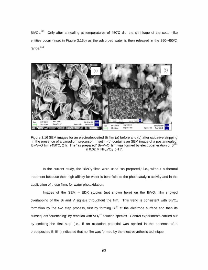
63
BiVO4.113 Only after annealing at temperatures of 450°C did the shrinkage of the cotton-like
entities occur (inset in Figure 3.16b) as the adsorbed water is then released in the 250–450°C
range.113
Figure 3.16 SEM images for an electrodeposited Bi film (a) before and (b) after oxidative stripping in the presence of a vanadium precursor. Inset in (b) contains an SEM image of a postannealed Bi–V–O film (450°C, 2 h. The “as prepared” Bi–V–O film was formed by electrogeneration of Bi3+
in 0.02 M NH4VO3, pH 7.
In the current study, the BiVO4 films were used “as prepared,” i.e., without a thermal
treatment because their high affinity for water is beneficial to the photocatalytic activity and in the
application of these films for water photoxidation.
Images of the SEM – EDX studies (not shown here) on the BiVO4 film showed
overlapping of the Bi and V signals throughout the film. This trend is consistent with BiVO4
formation by the two step process, first by forming Bi3+ at the electrode surface and then its
subsequent “quenching” by reaction with VO43− solution species. Control experiments carried out
by omitting the first step (i.e., if an oxidation potential was applied in the absence of a
predeposited Bi film) indicated that no film was formed by the electrosynthesis technique.

64
Figure 3.17A contains high resolution XPS spectra for a representative BiVO4 film in the
Bi 4f [Figure 3.17A (a)], V 2p [Fig. 3.17A (b)], and O 1s [Figure 3.17A (c)] binding energy regions.
The corresponding spectra for a film prepared from an authentic BiVO4 powder sample (see the
Experimental section) are included in Figure 3.17B for comparison.
Figure 3.17 High resolution XPS analyses of (A) (a) Bi 4f, (b) V 2p, and (c) O 1s for BiVO4 films prepared from BiCl3/NH4VO3, pH 7 and (B) corresponding spectra for a film prepared from
authentic BiVO4 powder.
Both samples in Figure 3.17 show the spin orbit splitting for Bi 4f7/2 and Bi 4f5/2 and for V
2p1/2 and V 2p3/2. These spectral data are in good accord with those reported for BiVO4 films
prepared by other techniques.39,41 Importantly, the Bi 4f7/2 and Bi 4f5/2 peaks appear at higher
energies than those for the metallic Bi located at 156.8 and 162.2 eV, respectively.114 The V 2p3/2

65
peak was found at 516.4 eV in the benchmark sample and slightly shifted to a higher energy for
the electrodeposited BiVO4 film [see Figure 3.17A(b) and 3.17B(b)]. As the reported position for
vanadium as V2O5 is 516.6 eV,115 considering the O 1s XPS data is necessary to ascertain the
chemical identity of the surface composition in the electrodeposited films. In the oxygen binding
energy region [(Figure 3.17A(c) and 3.17B(c)], the most dominant O 1s peak at 529.6 eV and
assigned to oxygen in a BiVO4 lattice environment41 is clearly seen in all our XPS spectra. For
the electrosynthesized samples, a shoulder at 531.7 eV, corresponding to OH− groups,114 is more
pronounced than that in the benchmark film. Similarly, a peak at 533.0 eV is associated with
oxygen in water116 and is present in the electrosynthesized samples consistent with their aqueous
preparative history and with the notion that these films contain adsorbed water. This is also
expected from the high hydrophilicity of BiVO4.
Coincidentally, the O 1s peak at 529.6 eV can also be assigned to oxygen in a V2O5
lattice environment;117 thus, the presence of surface V2O5 “contaminant” cannot be ruled out yet.
However, the XPS signals for the three element components (Bi, V, and O) are located at the
correct energies for BiVO4, and the surface atomic ratio of V to Bi is lower than the stoichiometric
ratio in all the cases, including for the benchmark BiVO4 where the V/Bi ratio is only 0.6. The V/Bi
ratio in the electrodeposited BiVO4 films was also close to this value for several films tested.
These findings rule out V2O5 as a component in the surface composition of the films as otherwise
they would have a V/Bi ratio > 1. If any oxide was formed during the stripping of Bi0 to Bi3+ in the
V5+ solution, it is Bi2O3. Bi2O3 formation is enhanced at basic pH values because of the
competition of OH− species present at high concentrations relative to the V5+ precursor species
for reaction with the freshly electrogenerated Bi3+. Therefore, our surface analysis data indicate a
thin Bi-rich surface layer to be always present atop the BiVO4 films. The commercial BiVO4
powder also shares this surface compositional feature, presumably stemming from its preparative
history. A Bi-rich surface layer was also reported by previous authors for BiVO4 formed by a
metallorganic decomposition route.41 This layer serves as a useful film photocorrosion protection
role in photoelectrochemical scenarios, as discussed in the next section.

66
3.5 Photoelectrochemical Behavior
Figure 3.18a contains a representative photocurrent/potential (iph/V) profile under
chopped visible light irradiation (0.1 Hz) for a BiVO4 film prepared in the NH4VO3 (pH 7) precursor
solution. These photoelectrochemical data were obtained in neutral media with Na2SO4 as a
supporting electrolyte to check the performance of the electrodeposited film for water
photooxidation. At pH ≥ 7, anodic iph/V profiles diagnostic of the n – type BiVO4 are seen in the
potential range extending from ~ 0.1 to 1.4 V, which also agree well with the data reported earlier
for BiVO4 films prepared by other routes.41,117 The iph onset potential at ~ 0.1 V is also as
expected for the conduction band position of BiVO4, corroborating its n – type semiconductor
behavior.
The photoaction spectral data further confirmed the identity of the electrodeposited BiVO4
films. One such spectrum is shown in Figure 3.18b. The medium was the same as in the
experiment considered in Figure 3.18a, and therefore, the data pertain to the photooxidation of
water. The good photoresponse from 350 to 580 nm yields a characteristic energy bandgap (Eg)
of 2.14 eV for BiVO4. The inset in Figure 3.18b contains the graphical analysis of the photoaction
spectral data leading to the above Eg value.

67
Figure 3.18(a) Photovoltammograms for a BiVO4 photoelectrode film prepared from BiCl3/NH4VO3
at pH 7 and measured in 0.1 M Na2SO4.
Figure 3.18(b) Corresponding photocurrent action spectrum recorded at 0.7 V. The inset contains analysis of these data according to the Butler method in Ref. 120. η is the quantum yield,
and hν is the photon energy (see also Ref. 120).

68
The analysis described by a previous author118 on the basis of the Gärtner mode119 was
used here, and the assumption of a direct bandgap is inherent in the plot contained in Figure.
3.18b. A direct gap was also assumed by previous authors for their analysis of
photoelectrochemical data on BiVO4 thin films prepared by a chemical solution approach.117 The
rationalization for a direct gap is available from the first principles electronic structure (density
functional theory or DFT) calculations for BiVO4.25 Incidentally, the Eg value obtained above is in
good accord with the value (2.1 eV) obtained from the DFT calculations for BiVO4 in the
monoclinic (scheelite) form.120 This structure modification and bandgap value are also generally
found for BiVO4 films and powders prepared by other methods.28,34,37,40,41,49,55 The
photoelectrochemical data were stable over several minutes, indicating that these films are
reasonably stable toward anodic photocorrosion. This work was developed as a proof-of-concept
study, and long term stability tests need to be carried out to assess the stability of the prepared
films.
3.6 Solution Combustion Synthesis of AgBiW2O8
Silver bismuth tungstate (AgBiW2O8) was another oxide semiconductor prepared by
combustion synthesis for the first time, and tested for its photocatalytic ability to degrade methyl
orange (MO), similar to the studies with BiVO4. The activity was compared to a sample of
AgBiW2O8 prepared by a solid state reaction.76 In addition to photodegradation of MO, another
crucial aspect was to demonstrate a proof-of-concept for photogeneration of syngas using
AgBiW2O8 particles.
3.6.1 Crystal Structure Modeling Considerations
To date, very little information is available on the exact crystal structure of AgBiW2O8.
The only structure of AgBiW2O8 we are aware of so far is the predicted monoclinic structure from
a previous study,76 which was speculated based on studies on three different oxides Ag2WO4,
Bi2W2O9, and AgBiW2O8. As mentioned earlier, the electronic band structure calculations were

69
performed by Dr. Huda and his group (Section 2.5). The results and the following discussion on
the crystal structure modeling and the band structure calculations have been included in the
present work to facilitate a better understanding of the band structure of AgBiW2O8.
Since the monoclinic structure was identified in a previous study,76
three possible
monoclinic structures, wolframite, scheelite, and fergusonite, were considered for the crystal
structure determination of AgBiW2O8. Figure 3.19 below shows the atomic arrangements for the
three crystal systems of AgBiW2O8. The calculations considered several possible relative sites
for Ag and Bi, and the lowest energy ones were chosen for the final calculations.
Figure 3.19 Structures of three possible lattices for AgBiW2O8 and their relative energy differences with respect to the wolframite structure. Purple, gray, yellow and red atoms are Bi, Ag, W and O,
respectively.

70
The scheelite structure is usually characterized by a tetragonal unit cell, but the
monoclinic CaWO4-d structure which is distorted from tetragonal symmetry appears to be
energetically favored. The wolframite and scheelite structures are closely related and transform
into one another depending on the cationic (R3+) radii.121 The higher atomic density in scheelite
structure is due to the fact that the supercell is double the size than in wolframite or fergusonite. On
the other hand, fergusonite, another distorted scheelite structure,122,123 also has a monoclinic unit
cell lattice. Both the fergusonite and wolframite supercells contain 24 atoms (two formula units)
each, whereas the scheelite supercell contains a total of 48 atoms (four formula units). From
DFT calculations, the wolframite structure (space group P 2/c; No. 13) was found to be the most
stable form with the lowest energy in terms of the possible relative sites for Ag and Bi atoms,
while the scheelite and fergusonite structures were 0.69 eV and 0.28 eV higher in energy,
respectively. This finding was in contrast to the earlier result which predicted a I 2/m space group
(No. 12) for AgBiW2O8.76 The rationalization for the wolframite structure was provided on the
following basis: The mineral structure for I 2/m symmetry has a hollendite structure, which cannot
accommodate a layered Ag-Bi-W-O network, and the bonding coordination also cannot
accommodate a W atom in this structure. Aluminum tungstate (space group C 2/m No. 12)
was also evaluated, but was found to be less stable than the wolframite structure. No other
structure with I 2/m symmetry was found to support the Ag-Bi-W-O network.
Wolframite belongs to the monoclinic space group P 2/c (No.13, Z=2)124 as in the AWO4
(A = Cd, Mn, Fe) family. In this structure, each W atom is coordinated to six O atoms, forming
octahedral WO6 structural units (Figure 3.19). Two distinct oxygen atoms (O1 and O2) occupy
two different sites in this structure: type O1 is connected to one tungsten atom with a shorter
bond length and to two A atoms with larger bond lengths, and type O2 is bonded to two different
W atoms and to one A atom. Thus the overall structure is made up of hexagonally close-packed
oxygen with certain octahedral sites occupied by A and W cations.125 For the present
calculations, a double unit cell of wolframite was used where the A-sites were replaced by Ag+
and Bi3+ selectively.

71
3.6.2 Electronic Structure Calculations
Figure 3.20 shows the band structure of the wolframite AgBiW2O8 structure (calculated by
Dr. Huda’s group) along the special symmetry points in the Brillouin zone. The calculations
predicted a minimum energy band gap of 1.96 eV, which is an indirect gap, where the conduction
band minimum occurs between the D and Z points. The existence of the long tails of absorption
curves for both SCS and SSR samples (diffuse reflectance data) indicated an indirect band gap
via (see diffuse reflectance data), in addition to the main optical transition. The minimum direct
gap of 2.02 eV was shown to occur between Y and E points. Both of these gaps are smaller than
the experimentally measured band gaps of 2.75 eV. However, this underestimation of energy
band gaps is generally a typical feature of DFT calculations.
Figure 3.20 Calculated band structure of wolframite AgBiW2O8. Here 0 eV refers to the highest occupied band (Fermi energy).

72
From the band structure calculations, it was shown that the valence band is divided into two
regions. The upper region was from the Fermi level (the highest occupied level) to – 0.5 eV, and
the second region starts from – 0.8eV. A gap of around 0.3 eV exists between these two regions.
The less dispersive bands along the Z to C points near the band gap indicated that electron or
hole transport across the oxygen layers (along the vertical direction in Figure 3.20) was not very
likely due to the higher electron effective mass in that direction. Hence, electronic conduction
was more likely to happen along the 2-D horizontal planes. The two relatively higher dispersion
regions (Y to E and D to Z in Figure 3.20) in the conduction band minima were due to the
presence of Bi-p levels, which also facilitates higher electron mobility relative to that of the holes.
The contribution from Ag 4d to the upper part of the valence band could be clearly seen
from the partial density-of-states (p-DOS) plot for AgBiW2O8 (Figure 3.21). Even at the topmost
part of the valence band the contribution from O-p is not significant. No contribution from the Bi-
s was observed, unlike the case of BiVO4 where Bi-s had an anti-bonding contribution at the top
of the valence band.25 The contributions of O-p and W-d around the band edges are similar to
that of the monoclinic WO3 parent structure.126
However, in AgBiW2O8, the presence of the Ag-d level “modulates” the valence band,
and is also responsible for the uplift of the valence band edge compared to the WO3 case. Bi-p
was found to contribute to the conduction band minimum, though the lower part of the conduction
band is dominated by W-d levels. Even though the O 2p and Bi 6p orbital contributions are small
around both the band edges, their presence would facilitate favorable p-d optical transitions.
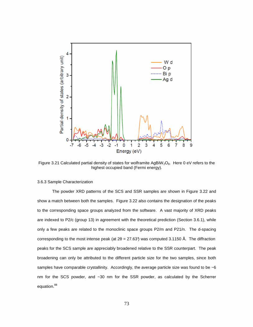
73
Figure 3.21 Calculated partial density of states for wolframite AgBiW2O8. Here 0 eV refers to the highest occupied band (Fermi energy).
3.6.3 Sample Characterization
The powder XRD patterns of the SCS and SSR samples are shown in Figure 3.22 and
show a match between both the samples. Figure 3.22 also contains the designation of the peaks
to the corresponding space groups analyzed from the software. A vast majority of XRD peaks
are indexed to P2/c (group 13) in agreement with the theoretical prediction (Section 3.6.1), while
only a few peaks are related to the monoclinic space groups P2/m and P21/n. The d-spacing
corresponding to the most intense peak (at 2θ = 27.63°) was computed 3.1150 Å. The diffraction
peaks for the SCS sample are appreciably broadened relative to the SSR counterpart. The peak
broadening can only be attributed to the different particle size for the two samples, since both
samples have comparable crystallinity. Accordingly, the average particle size was found to be ~6
nm for the SCS powder, and ~30 nm for the SSR powder, as calculated by the Scherrer
equation.88

74
Figure 3.22 XRD spectra of the combustion synthesized (CS) and solid state (SSR) synthesized AgBiW2O8.
Consistent with the smaller particle size, the SCS samples also have a higher surface
area (by an order of magnitude) relative to the SSR counterpart. Table 3.3 shows a comparison
of the BET surface area values of the SCS and the SSR samples. It is also evident from these
data that the SSR sample prepared in this work has a somewhat higher surface area than that
quoted in a previous study. The superior dispersion of the SCS sample relative to the SSR
counterpart, is entirely consistent with the feature that the high reaction temperatures attained in
solution combustion synthesis,2,14 result in a finely dispersed and porous morphology for the
synthesized product. This is all the more desirable given that solution combustion synthesis yields
the product in minutes as opposed to the several hours-long synthesis times spanned in solid-
state reaction routes.

75
Table 3.3. Comparison of surface area of AgBiW2O8 nanoparticles prepared by solution combustion synthesis and solid-state reaction
Photocatalyst Micropore Area
cm2 External Surface Area
cm2 BET Surface Area
m2 g-1 Comment
SCS-AgBiW2O8 5.488 28.938 34.436 This work
SSR-AgBiW2O8 0.136 0.406 0.542 This work
SSR-AgBiW2O8 - - 0.29 Ref. 7
Representative TEM images of the SCS–AgBiW2O8 are shown in Figure 3.23. The
images show mainly spherical nanocrystalline particles in 5 – 10 nm range, which are in accord
with the particle size calculated by the Scherrer equation. It is worth mentioning that the samples
were obtained by solution combustion synthesis even without a post annealing treatment step.
This is yet another crucial advantage with this synthesis approach from an energy input
perspective to add to its high time efficiency, as mentioned in the introduction section.
Figure 3.23 TEM images of solution combustion synthesized AgBiW2O8.

76
Figures 3.24 (a) and 3.24 (b) contain the UV-visible diffuse reflectance data on the SCS
and SSR synthesized AgBiW2O8 samples, respectively. The absorption plots in the inset show
an extension of the absorption edge into the visible region. The band gap (Eg) values of the
powders, estimated from the Tauc plots of the square root of the Kubelka–Munk function versus
the photon energy, 90 were found to be 2.74 eV for the SCS sample, and 2.77 eV for the SSR
sample. These values are in very good agreement with a the value (2.75 eV) reported for this
complex oxide in a previous study on solid state synthesis.76 The long wavelength absorption tail
(Figure 3.24 insets) is not attributed to the surface plasmon absorption of Ag metal (490 – 530
nm), since Ag0 was not detected on the surface of the AgBiW2O8 nanoparticles, which is shown
from the XPS analysis described in the following section.

77
Figure 3.24 Tauc plots for (a) SCS-AgBiW2O8 and (b) SSR-AgBiW2O8. Insets contain the percent
transmittance data for both samples.

78
Figure 3.25 contains the high-resolution XPS data for the SCS–AgBiW2O8 samples in the
binding energy regimes (3d for Ag, 4f for Bi and W, and 1s for O) characteristic of the four
elements in the compound. The Pt 4f signals for the Pt modified AgBiW2O8 are also shown in the
figure.
Figure 3.25 High-resolution core level X-ray photoelectron spectra (ordinates in the spectra in counts per second) in the (a) Ag 3d, (b) Bi 4f, (c) W 4f, (d) O 1s and (e) Pt 4f binding energy
regimes for SCS-AgBiW2O8 (a-d) and Pt-modified SCS-AgBiW2O8. .
The XPS signals for the metal components are split due to spin-orbit coupling. The
signals are located at 387.9 eV for silver (Ag 3d5/2), at 158.9 eV for bismuth (Bi 4f5/2) and at 35.1
eV for tungsten (W 4f7/2) respectively.114 These respective peaks for Ag, Bi and W are associated
with Ag+ or Ag2+ in an oxide structure, with Bi3+ also surrounded by oxygen neighbors (such as in
Bi2O3, Bi2O4), and with W6+ in a hexagonal oxygen-bonded structure (such as WO3, H2WO4).127
The XPS data are in accord with a layered structure for AgBiW2O8 composed of WO6 octahedral
sheets interleaved with Bi-O-Bi layers and AgOx polyhedra. Importantly, the XPS data also

79
confirm that there is no free metal formation (i.e., Ag0, Bi0) during SCS. For instance, in the Bi
binding energy regime, it must be noted that the Bi 4f7/2 and Bi 4f5/2 signals in Figure 3.25b are
located at 158.95 and 164.2 eV; far higher in energy than the characteristic peaks for metallic Bi
located at 156.8 eV and 162.2 eV respectively.127 Similar considerations apply for silver peaks as
well.127
In the O 1s binding energy regime, the peak at 529.9 eV is in good agreement with that
similarly reported for a bismuth tungstate structure127 and at variance with that for WO3 at 530.5
eV.128 The other O 1s peak at 532.1 eV is assignable to residual water bound to the oxide
particles and also to water molecules adsorbed on the sample surface.129
Furthermore, the XPS profiles of the powder samples after the dye degradation and
syngas photogeneration reactions did not show any shift in the binding energy, which is an
indication that the composition of the sample was stable after photocatalysis.
3.7 Photocatalytic Behavior of AgBiW2O8
3.7.1 Photodegradation of Methyl Orange
The photocatalytic activity of the CS and SSR powders was evaluated under visible light
irradiation using methyl orange as a probe material. The results of MO photodegradation in the
form of a concentration – time plot, are presented in Figure 3.26. The figure contains the
degradation profiles as a function of time for the blank (no photocatalyst) case, and for the SCS–
and SSR – AgBiW2O8 samples. The extent of photodegradation of MO was measured by the
decrease in absorbance. The data were plotted taking the time at the start of light irradiation i.e.,
after 30 min of adsorption in the dark, as the initial time.

80
Figure 3.26 Comparison of methyl orange photodegradation profiles (fractional concentration vs irradiation time) for the blank case (no oxide photocatalyst) and for the two photocatalyst SCS–
and SSR–AgBiW2O8 powders.
The results indicate the superior activity of the SCS sample over the SSR sample. For
example, ~ 60% of the dye was degraded by the SCS sample in about 2 h, while the SSR sample
showed a degradation of ~ 20 in the same time. The superior activity of the SCS sample is
rooted in the morphological factors (Table 3.3), with a higher surface area for the SCS sample. It
is known that smaller size and higher surface area increase the photocatalytic activity due to
enhanced charge carrier photogeneration and separation.
The degradation profiles in Figure 3.26 indicate a pseudo first order kinetic rate for the
photocatalysis reactions, and the data match well with the model of the pseudo first order kinetics

81
plotted in Figure 3.27. The solid line indicates the least squares linear fit for the kinetic data
plotted as a dotted line with circles for data points.
Figure 3.27 Kinetic data for the MO degradation profiles with the SCS– and SSR–AgBiW2O8.
The apparent rate constants calculated from the slopes of the lines were 0.0102 min–1 for
the SCS sample and 0.0018 min–1 for the SSR sample. The rate was higher for the SCS
nanoparticles when compared to the SSR reference, which is indicative of its better photocatalytic
performance. This could be explained on the basis of the morphological differences between the
two samples. The smaller size of the SCS particles leads to enhanced charge carrier generation
and more effective separation of the photogenerated charge carriers, resulting in an enhanced
degradation rate.
Similar to the case with BiVO4, MO degradation is assumed to be by photocatalysis and
photosensitization pathways.47 Degradation by photolysis is negligible in this case, as evident from

82
the MO blank data in Figure 3.26. The possible degradation mechanism is outlined below by the
following equations.
Photosensitization pathway
(3.23) OH CO OH MO
(3.22) OH OH e OH
(3.21) OH H O )(e ABW
(3.20) ABW O O )(e ABW
(3.19) )(e ABW MO ABW MO(3.18) MO hν MO
22
--22
222-
22-
-
+→→+
+→+
→++
+→+
+→+
→+
•
•
+•−
•−
•+∗
∗
Photocatalysis pathway
(3.30) OH CO OH MO
(3.29) OH OH e OH
(3.28) OH H O )ABW(e
(3.27) ABW O O )(e ABW
(3.26) ABW H OH )(h ABW OH
(3.25) ABW MO )(h ABW MO
(3.24) )(h ABW )(e ABW h ABW
22
--22
222-
22-
2
-
+→→+
+→+
→++
+→+
++→+
+→+
+→+
•
•
+•−
•−
+•+
•++
+ν
The role of O2 is elucidated from equations (5) and (12). The conduction band electrons on
the photocatalyst surface are scavenged by O2 forming the superoxide radical (O2–•). The
superoxide radical forms ●OH species, which then causes the indirect degradation of MO.47,108
3.7.2. Photogeneration of syngas (CO +H2) and Methane on Pt – modified AgBiW2O8
In addition to MO photodegradation, the SCS – AgBiW2O8 oxide was also studied for its
ability to photogenerate syngas (CO + H2) from formic acid (HCOOH) and methane (CH4) from
acetic acid (H3CCOOH). This particular aspect was aimed towards developing a proof-of-concept
study for generation of syngas from CO2 reduction, CO2 being generated in situ from formic acid
degradation. For this purpose, the AgBiW2O8 nanoparticles were loaded with 1 mass percent Pt
using a photodeposition procedure.86 The color of the Pt – modified oxide particles changed

83
significantly from light yellow to a grayish hue as illustrated in Figure 3.28 below. The oxide powder
was then loaded into a Pyrex photoreactor containing 200 ml of a deaerated solution (N2 purged) of
0.1 M HCOOH or 0.1 M H3CCOOH containing at a dose of 2 g/L. The UV lamp (400 W medium-
pressure Hg arc) was turned on and the gaseous products evolved were analyzed by gas
chromatography.
Figure 3.28 SCS–AgBiW2O8 powder (a) before and (b) after surface modification with 1 wt % Pt.
Figure 3.29 compares the temporal evolution of the gaseous products for formic acid
(Figure 3.29a) and acetic acid (Figure 3.29b) as the electron donor. Control experiments carried
out without photocatalyst powder did not yield any gaseous products indicating negligible acid
photolysis. In addition, in the methane photogeneration experiments, another set of controls
without initial Pt modification were also carried out, to assess the effect of Pt on H2 and CH4
photogeneration.
(b) (a)

84
Figure 3.29 Temporal profiles of the gaseous products formed in the photocatalytic reaction of AgBiW2O8-Pt from (a) formic acid and (b) acetic acid as electron donors. Both systems were
saturated with N2.

85
A noticeable feature of this experiment is that HCOOH acts as an in situ precursor for
CO2 generation (Figure 3.29a). The advantages of using formate species is two fold. First, the
direct electrochemical reduction of CO2 in aqueous media is difficult due to the low partial
pressure of CO2 in the atmosphere (3.9 x 10⁻⁴ atm) and by its low solubility in water (1.5 g/L at
298 K), 130 and second, the formate species have high solubility in water (945 g/L at 298 K).131 In
addition, the formate species have high proclivity for being adsorbed on oxide semiconductor
surfaces132 and are easily oxidized by the photogenerated holes in the oxide.
In both cases (Figures 3.29a and b), the photoreaction is initiated by photooxidation of
the respective carboxylic acid (photo-Kolbe reaction) on the oxide photocatalyst surface. The
●OH radicals photogenerated from the initial hole (h+vb) attack on the surface adsorbed water
molecules cause carboxylic acid oxidation rather than O2 generation from photooxidation of water.
H2 photogeneration on Pt sites occurs in both cases although initial Pt modification of the oxide
surface has different consequences. In the case of formic acid as the electron donor, H2
photogeneration is completely quenched in the absence of Pt while for acetic acid (Figure 3.29b),
the extent of methane photogeneration is influenced by the presence of Pt islands on the oxide
surface.
Rationalization of the above observations can be done by considering the radical
intermediates that are generated on initial photo-oxidation of the organic acid. In the case of
formic acid oxidation, the intermediate photogenerated HCOO● radical injects an electron into the
AgBiW2O8 conduction band via the well-established current–doubling mechanism (shown in
Figure 3.30a).133 The net result is formation of hydrogen atoms (on Pt sites followed by
subsequent H2 formation) and CO2. No poisoning of the Pt sites was observed attesting to the
site specificity visualized for CO2 reduction and proton reduction on the bare semiconductor
surface and Pt islands respectively.
In the second case for acetic acid, the corresponding H3CCOO● photogenerated radical
(formed from initial hole attack on acetate) rapidly decomposes to H3C● + CO2, and then the H3C
●
radicals react with the hydrogen atoms stored on Pt islands to ultimately get converted into CH4

86
(Figure 3.30b). Absence of the Pt sites inhibits the surface reaction involving the methyl radicals
and hydrogen atoms. Figure 3.30 summarizes the mechanistic paths for the photocatalytic Kolbe
reaction plus other reactions occurring on irradiation of Pt-modified SCS-AgBiW2O8 nanoparticles
in contact with HCOOH (Figure 3.30a) and H3CCOOH (Figure 3.30b) respectively.
Rate constants of the reactions associated with the photogenerated electrons are
indicated as k(x) (with x = 1 to 4). The reaction product profiles are consistent with an ordering of
these rate constants: k(1) > k(2) ~ k(4) > k(3). The very low amount of H2 formed in the case of
acetic acid is consistent with k(1) > k(4) which means that the photoelectrons are mainly
consumed in the generation of CH4 from the methyl radical. Importantly no C2H6 was found in our
experiments indicating that the conduction band electrons are transferred to H3C● thus cancelling
out the radical-radical coupling. The uptake of e–cb from Pt-modified SCS-AgBiW2O8 is much
higher by H3C● than by CO2 (k(1) > k(3)) and therefore no CO is observed in the data for
CH3COOH (Figure 3.29b). Further, k(2) > k(3) which would be consistent with the ratio,
H2 : CO ~ 3 : 1, measured for formic acid as the electron donor.

87
Figure 3.30 Mechanistic pathways for the photocatalytic Kolbe reaction along with other reactions
occurring on irradiation of Pt-modified SCS-AgBiW2O8 nanoparticles in contact with (a) formic acid and (b) acetic acid respectively.
(a)
(b)

88
In the absence of irradiation, the products and pathways of electrochemical oxidation of
the two carboxylic acids (Kolbe reaction) depend on the anode material.134 On a platinum
electrode and with simple carboxylic acids such as H3CCOOH, the Kolbe reaction (performed by
galvanostatic electrolysis) involves the formation of hydrocarbons through a free radical sequence
as follows134: (H3CCOO¯ � H3CCOO● � H3C● + CO2, 2 H3C
● � C2H6). Thus, the normal Kolbe
reaction involves radical-radical coupling (H3C● coupling) as the predominant mechanism at
platinum anodes while an abnormal Kolbe reaction almost exclusively occurs at carbon
electrodes either in organic or in aqueous media generating CH3COOCH3.134 With α-substituted
carboxylic acids, more complex mechanisms involving radicals and/or carbonium ion
intermediates give rise to the formation of other products such as olefins, alcohols, ethers, and
esters.135
Interesting contrasts have been reported in product evolution for similar electrode
surfaces with and without illumination.136-139 Ethane (C2H6) was observed as the dominant
product on a TiO2 photoanode in organic media (acetonitrile) with 0.1 M tetrabutyl ammonium
perchlorate as supporting electrolyte and 0.08 M of tetrabutyl ammonium acetate as source of
acetate ions.136 On the other hand, methane (rather than ethane) was reported on
photoirradiated TiO2-Pt nanoparticles in contact with acetic acid very similar to the observations in
this study (Figure 3.29b). Methyl radical coupling (leading to ethane) is clearly favored on the
massive electrode surface because of the site proximity effect.
Quantum yields for the formation of syngas (H2+CO) and CO2 in the formic acid solution
were as follows: H2 = 3.0 %, CO = 0.8 % and CO2 = 4.5 %. [Chemical actinometry using an
aqueous solution of 6 mM K3Fe(C2O4)3.3H2O in 1.0 N H2SO4 140 provided a calculated photon flux
of 3.2 x 10⁻² moles and thus the reported quantum yield was calculated as the percent ratio of
the number of moles of product divided by the moles of photons.] The H2:CO2 ratio was seen to
be ~ 1:1.5 for reaction times up to 1 hr, whereas it reached a ratio of 1:2.8 for reaction times
higher than 3 h. Product amounts at the end of the photocatalytic runs were as follows:
H2 = 1.0 × 10⁻² mol/g.L, CO = 3.0 × 10⁻³ mol/g.L and CO2 = 2.8 × 10⁻² mol/g.L. These data are

89
reported as the number of moles of product divided by the photocatalyst mass and liquid volume
in the photoreactor. The turnover number (TON = molar amount of reacted electrons divided by
molar amount of catalyst) for the photocatalytic formation of H2 + CO (using a factor 2 to
represent the number of electrons per H2 and CO respectively) on the Pt-modified SCS–
AgBiW2O8 nanoparticles reached a value of ca. 4.3 after 4 h irradiation, producing 1.0 mmol of H2
and 0.3 mmol of CO.
For the photocatalytic synthesis of CH4 from acetic acid on Pt-modified SCS–AgBiW2O8
nanoparticles, the amount of gases generated at the end of the runs was as follows:
CH4 = 1.45 x 10⁻² mol/g.L, CO2 = 0.92 x 10⁻² mol/g.L and H2 = 0.24 x 10⁻² mol/g.L, with the
quantum yields as follows: CH4 = 1.7 %, CO2 = 1.2 % and H2 = 0.3 %. The experimental
CH4:CO2 ratio was found to be ~ 1.5:1 at reaction times up to 1 h, increasing slightly afterwards to
1.6:1.

90
CHAPTER 4
SUMMARY AND CONCLUSIONS
There has been an exponential increase in the research for developing new oxide
photocatalysts for solar energy and environmental remediation applications, especially during the
past decade. Combined with the advances in nanotechnology, the activity and applications of
oxide photocatalysts have increased substantially, ranging from air and water purification, solar
induced hydrogen production, self cleaning devices to microbial disinfection etc.
As part of the search for new oxide photocatalysts, the present dissertation focused on
preparing bismuth based oxide photocatalysts of the Bi-M-O (M = V or W) family using ‘mild’
synthesis routes (electrodeposition and combustion synthesis)2,10-15,87 and evaluating their
efficacy for solar energy and environmental remediation applications. These preparation
methods are simple, less time consuming, and more importantly, reduce the energy payback time
of the prepared materials. Two such oxides namely, bismuth vanadate (BiVO4) and silver
bismuth tungstate (AgBiW2O8), were prepared during the course of this research.
The photocatalytic activity of the oxide photocatalysts was assessed by studying the
degradation of methyl orange (MO) dye under visible light irradiation. Both the compounds
showed superior photocatalytic activity when compared to the respective benchmark samples.
Another crucial aspect of this study was to test the ability of the oxides to photocatalytically
generate fuels from aqueous solutions of carboxylic acids. The ability of photocatalysts to
produce fuels from sources such as CO2 is beneficial from an energy perspective. This aspect
was the basis for studying the syngas photogeneration capacity of AgBiW2O8 in the present work.
Part I of the study focused on preparing BiVO4 by solution combustion synthesis and its
photocatalytic activity was assessed using MO degradation. The effect of the vanadium
precursor on the photocatalytic activity was probed for the first time in this study, and it was found

91
that the choice of vanadium precursor influenced the photocatalytic performance of BiVO4. In
addition, BiVO4 photoelectrodes were also prepared on a Pt substrate by electrodepostion.
Part II of the study comprised of preparing AgBiW2O8 photocatalyst by solution
combustion synthesis. AgBiW2O8 was prepared for the first time using the combustion synthesis
technique in this study. The combustion–synthesized sample showed superior MO
photodegradation ability relative to a benchmark sample prepared by solid state reaction, which is
explained based on the morphological differences in the samples.
Another important aspect of this work was to assess syngas (H2 + CO) photogeneration
capacity of SCS-AgBiW2O8 from an aqueous solution of formic acid, as well as methane (CH4)
photogeneration from an aqueous solution of acetic acid. Pt was photodeposited on the oxide
surface and it was observed that H2 and CH4 photogeneration capacities were affected by the Pt
loading. The reaction mechanisms were found to be different in both the cases.
Overall, the focus of the research was to prepare oxide semiconductors using ‘mild’
synthesis methods and to evaluate their potential for solar energy and environmental remediation
applications. The results were promising in that the photocatalytic activity was superior to the
respective benchmark samples. Further studies aimed at increasing the sensitivity of the
materials towards visible light need to be carried out to enhance the use of these materials under
solar irradiation.

92
REFERENCES
(1) Rajeshwar, K. Journal of Applied Electrochemistry 2007, 37, 765-787.
(2) Rajeshwar, K.; de Tacconi, N. R. Chemical Society Reviews 2009, 38, 1984-1998.
(3) Linsebigler, A. L.; Lu, G. Q.; Yates, J. T. Chemical Reviews 1995, 95, 735-758.
(4) http://www.lbl.gov/Science-Articles/Archive/MSD-full-spectrum-solar-cell.html.(accessed 07/2011).
(5) Bard, A. J., Faulkner, L. R. Electrochemical methods: fundamentals and applications; 2nd Ed ed.; John Wiley & Sons: NJ, 2001.
(6) Zhang, H. J.; Chen, G. H.; Bahnemann, D. W. Journal of Materials Chemistry 2009, 19, 5089-5121.
(7) Kudo, A.; Miseki, Y. Chemical Society Reviews 2009, 38, 253-278.
(8) Sohrabi, M.; Tavakoli, A.; Kargari, A. Chemical Papers 2007, 61, 151-170.
(9) Lincot, D. Thin Solid Films 2005, 487, 40-48.
(10) Schlesinger, T. E. R., K.; de Tacconi, N. R. Electrodeposition of Semiconductors; 5th ed.; Springer: New York, 2010.
(11) Kamath, P. V.; Therese, G. H. A. Chemistry of Materials 2000, 12, 1195-1204.
(12) Simka, W.; Puszczyk, D.; Nawrat, G. Electrochimica Acta 2009, 54, 5307-5319.
(13) Patil, K. C., Hegde, M.S., Rattan, Tanu, Aruna, S.T. Chemistry of Nanocrystalline Oxide Materials: Combustion Synthesis, Properties and Applications; World Scientific Publishing Pte. Ltd.: Singapore, 2008.
(14) Aruna, S. T.; Mukasyan, A. S. Current Opinion in Solid State & Materials Science 2008, 12, 44-50.
(15) Mukasyan, A. S.; Epstein, P.; Dinka, P. Proceedings of the Combustion Institute 2007, 31, 1789-1795.
(16) Moore, J. J.; Feng, H. J. Progress in Materials Science 1995, 39, 243-273.
(17) Merzhanov, A. G. Journal of Materials Chemistry 2004, 14, 1779-1786.

93
(18) Jain, S. R.; Adiga, K. C.; Verneker, V. R. P. Combustion and Flame 1981, 40, 71-79.
(19) Smith, H. M. High Performance Pigments; Wiley - VCH: Weinheim, Germany, 2002.
(20) Rajeshwar, K., McConnell, R., Licht, S. (Eds.) Solar Hydrogen Generation; Springer: New York, 2008.
(21) Rajeshwar, K., Ibanez, J.G. Environmental Electrochemistry; Academic Press: San Diego, 1997.
(22) Qurashi, M. M., Barnes, W.H. Am.Mineralogist 1952, 37, 423.
(23) Sleight, A. W.; Chen, H. Y.; Ferretti, A.; Cox, D. E. Materials Research Bulletin 1979, 14, 1571-1581.
(24) Bhattacharya, A. K.; Mallick, K. K.; Hartridge, A. Materials Letters 1997, 30, 7-13.
(25) Walsh, A.; Yan, Y.; Huda, M. N.; Al-Jassim, M. M.; Wei, S. H. Chemistry of Materials 2009, 21, 547-551.
(26) Tokunaga, S.; Kato, H.; Kudo, A. Chemistry of Materials 2001, 13, 4624-4628.
(27) Kudo, A.; Omori, K.; Kato, H. Journal of the American Chemical Society 1999, 121, 11459-11467.
(28) Kudo, A.; Ueda, K.; Kato, H.; Mikami, I. Catalysis Letters 1998, 53, 229-230.
(29) Oshikiri, M.; Boero, M.; Ye, J. H.; Zou, Z. G.; Kido, G. Journal of Chemical Physics 2002, 117, 7313-7318.
(30) Kohtani, S.; Makino, S.; Kudo, A.; Tokumura, K.; Ishigaki, Y.; Matsunaga, T.; Nikaido, O.; Hayakawa, K.; Nakagaki, R. Chemistry Letters 2002, 660-661.
(31) Liu, J. B.; Wang, H.; Wang, S.; Yan, H. Materials Science and Engineering B-Solid State Materials for Advanced Technology 2003, 104, 36-39.
(32) Kohtani, S.; Koshiko, M.; Kudo, A.; Tokumura, K.; Ishigaki, Y.; Toriba, A.; Hayakawa, K.; Nakagaki, R. Applied Catalysis B-Environmental 2003, 46, 573-586.
(33) Kohtani, S.; Hiro, J.; Yamamoto, N.; Kudo, A.; Tokumura, K.; Nakagaki, R. Catalysis Communications 2005, 6, 185-189.
(34) Liu, H. M.; Nakamura, R.; Nakato, Y. Journal of the Electrochemical Society 2005, 152, G856-G861.
(35) Zhang, C.; Zhu, Y. F. Chemistry of Materials 2005, 17, 3537-3545.
(36) Gotic, M.; Music, S.; Ivanda, M.; Soufek, M.; Popovic, S. Journal of Molecular Structure 2005, 744, 535-540.
(37) Zhou, L.; Wang, W. Z.; Liu, S. W.; Zhang, L. S.; Xu, H. L.; Zhu, W. Journal of Molecular Catalysis a-Chemical 2006, 252, 120-124.

94
(38) Yu, J. Q.; Kudo, A. Advanced Functional Materials 2006, 16, 2163-2169.
(39) Zhang, L.; Chen, D. R.; Jiao, X. L. Journal of Physical Chemistry B 2006, 110, 2668-2673.
(40) Long, M.; Cai, W. M.; Cai, J.; Zhou, B. X.; Chai, X. Y.; Wu, Y. H. Journal of Physical Chemistry B 2006, 110, 20211-20216.
(41) Sayama, K.; Nomura, A.; Arai, T.; Sugita, T.; Abe, R.; Yanagida, M.; Oi, T.; Iwasaki, Y.; Abe, Y.; Sugihara, H. Journal of Physical Chemistry B 2006, 110, 11352-11360.
(42) Xie, B. P.; Zhang, H. X.; Cai, P. X.; Qiu, R. L.; Xiong, Y. Chemosphere 2006, 63, 956-963.
(43) Zhang, X.; Ai, Z. H.; Jia, F. L.; Zhang, L. Z.; Fan, X. X.; Zou, Z. G. Materials Chemistry and Physics 2007, 103, 162-167.
(44) Chen, X. Y.; Zhang, Z. J.; Lee, S. W. Journal of Solid State Chemistry 2008, 181, 166-174.
(45) Long, M. C.; Beranek, R.; Cai, W. M.; Kisch, H. Electrochimica Acta 2008, 53, 4621-4626.
(46) Chatchai, P.; Murakami, Y.; Kishioka, S. Y.; Nosaka, A. Y.; Nosaka, Y. Electrochemical and Solid State Letters 2008, 11, H160-H163.
(47) Ge, L. Journal of Molecular Catalysis a-Chemical 2008, 282, 62-66.
(48) Jiang, H. Q.; Endo, H.; Natori, H.; Nagai, M.; Kobayashi, K. Journal of the European Ceramic Society 2008, 28, 2955-2962.
(49) Strobel, R.; Metz, H. J.; Pratsinis, S. E. Chemistry of Materials 2008, 20, 6346-6351.
(50) Zhao, Y.; Xie, Y.; Zhu, X.; Yan, S.; Wang, S. X. Chemistry-a European Journal 2008, 14, 1601-1606.
(51) Zhang, X. F.; Chen, S.; Quan, X.; Zhao, H. M. Separation and Purification Technology 2009, 64, 309-313.
(52) Chatchai, P.; Murakami, Y.; Kishioka, S. Y.; Nosaka, A. Y.; Nosaka, Y. Electrochimica Acta 2009, 54, 1147-1152.
(53) Zhang, A. P.; Zhang, J. Z. Spectrochimica Acta Part a-Molecular and Biomolecular Spectroscopy 2009, 73, 336-341.
(54) Yu, J. Q.; Zhang, Y.; Kudo, A. Journal of Solid State Chemistry 2009, 182, 223-228.
(55) Yin, W. Z.; Wang, W. Z.; Shang, M.; Zhang, L.; Ren, J. Chemistry Letters 2009, 38, 422-423.
(56) Dunkle, S. S.; Helmich, R. J.; Suslick, K. S. Journal of Physical Chemistry C 2009, 113, 11980-11983.
(57) Sun, S. M.; Wang, W. Z.; Zhou, L.; Xu, H. L. Industrial & Engineering Chemistry Research 2009, 48, 1735-1739.

95
(58) Li, H. B.; Liu, G. C.; Duan, X. C. Materials Chemistry and Physics 2009, 115, 9-13.
(59) Ke, D. N.; Peng, T. Y.; Ma, L.; Cai, P.; Dai, K. Inorganic Chemistry 2009, 48, 4685-4691.
(60) Wang, F. X.; Shao, M. W.; Cheng, L.; Hua, J.; Wei, X. W. Materials Research Bulletin 2009, 44, 1687-1691.
(61) Sun, Y. F.; Wu, C. Z.; Long, R.; Cui, Y.; Zhang, S. D.; Xie, Y. Chemical Communications 2009, 4542-4544.
(62) Shang, M.; Wang, W. Z.; Sun, S. M.; Ren, J.; Zhou, L.; Zhang, L. Journal of Physical Chemistry C 2009, 113, 20228-20233.
(63) Zhang, A. P.; Zhang, J. Z. Materials Letters 2009, 63, 1939-1942.
(64) Dong, F. Q.; Wu, Q. S.; Ma, J.; Chen, Y. J. Physica Status Solidi a-Applications and Materials Science 2009, 206, 59-63.
(65) Zhang, A. P.; Zhang, J. Z.; Cui, N. Y.; Tie, X. Y.; An, Y. W.; Li, L. J. Journal of Molecular Catalysis a-Chemical 2009, 304, 28-32.
(66) Ma, D. K.; Wang, S.; Cai, P.; Jiang, J. L.; Yang, D. P.; Huang, S. M. Chemistry Letters 2009, 38, 962-963.
(67) Zhang, X. F.; Zhang, Y. B.; Quan, X.; Chen, S. Journal of Hazardous Materials 2009, 167, 911-914.
(68) Yin, W. Z.; Wang, W. Z.; Zhou, L.; Sun, S. M.; Zhang, L. Journal of Hazardous Materials 2010, 173, 194-199.
(69) Yang, T.; Xia, D. G. Journal of Crystal Growth 2009, 311, 4505-4509.
(70) Sayama, K.; Wang, N. N.; Miseki, Y.; Kusama, H.; Onozawa-Komatsuzaki, N.; Sugihara, H. Chemistry Letters 2010, 39, 17-19.
(71) Dall'Antonia, L. H.; de Tacconi, N. R.; Chanmanee, W.; Timmaji, H.; Myung, N.; Rajeshwar, K. Electrochemical and Solid State Letters 2010, 13, D29-D32.
(72) Jiang, H. Q.; Nagai, M.; Kobayashi, K. Journal of Alloys and Compounds 2009, 479, 821-827.
(73) Lee, D. K.; Cho, I. S.; Lee, S.; Bae, S. T.; Noh, J. H.; Kim, D. W.; Hong, K. S. Materials Chemistry and Physics 2010, 119, 106-111.
(74) Roy, B.; Fuierer, P. A. Journal of Materials Research 2009, 24, 3078-3086.
(75) Timmaji, H. K., Chanmanee, W., de Tacconi, N.R., Rajeshwar, K Journal of Advanced Oxidation Technologies 2011, 14, 93-105.
(76) Tang, J. W.; Ye, J. H. Journal of Materials Chemistry 2005, 15, 4246-4251.

96
(77) Shi, H. F.; Li, Z. S.; Ye, J. H.; Zou, Z. G. Journal of Physics D-Applied Physics 2010, 43, 085402-1-085402-7.
(78) Shi, H. F.; Huang, X. L.; Tian, H. M.; Lv, J.; Li, Z. S.; Ye, J. H.; Zou, Z. G. Journal of Physics D-Applied Physics 2009, 42, -.
(79) Kato, H.; Matsudo, N.; Kudo, A. Chemistry Letters 2004, 33, 1216-1217.
(80) Tang, J. W.; Zou, Z. G.; Ye, J. H. Angewandte Chemie-International Edition 2004, 43, 4463-4466.
(81) Zhang, L. S.; Wong, K. H.; Chen, Z. G.; Yu, J. C.; Zhao, J. C.; Hu, C.; Chan, C. Y.; Wong, P. K. Applied Catalysis a-General 2009, 363, 221-229.
(82) Ouyang, S.; Li, Z.; Ouyang, Z.; Yu, T.; Ye, J.; Zou, Z. The Journal of Physical Chemistry C 2008, 112, 3134-3141.
(83) Chueh, W. C.; Falter, C.; Abbott, M.; Scipio, D.; Furler, P.; Haile, S. M.; Steinfeld, A. Science 2010, 330, 1797-1801.
(84) Lehn, J. M.; Ziessel, R. Proceedings of the National Academy of Sciences of the United States of America-Physical Sciences 1982, 79, 701-704.
(85) Ziessel, R.; Hawecker, J.; Lehn, J. M. Helvetica Chimica Acta 1986, 69, 1065-1084.
(86) de Tacconi, N. R.; Chenthamarakshan, C. R.; Rajeshwar, K.; Lin, W. Y.; Carlson, T. F.; Nikiel, L.; Wampler, W. A.; Sambandam, S.; Ramani, V. Journal of the Electrochemical Society 2008, 155, B1102-B1109.
(87) Dean, J. A. Analytical Chemistry Handbook; McGraw-Hill, Inc.: New York, 1995.
(88) Cullity, B. D. Elements of X-Ray Diffraction; Addison-Wesley: Reading, MA, 1967.
(89) Pankove, J. L. Optical Processes in Semiconductors; Prentice Hall: Englewood, Cliffs, New Jersey, 1971.
(90) Finlayson, A. P.; Tsaneva, V. N.; Lyons, L.; Clark, M.; Glowacki, B. A. Physica Status Solidi a-Applications and Materials Science 2006, 203, 327-335.
(91) Hawecker, J.; Lehn, J. M.; Ziessel, R. Helvetica Chimica Acta 1986, 69, 1990-2012.
(92) Lin, W. Y.; Wei, C.; Rajeshwar, K. Journal of the Electrochemical Society 1993, 140, 2477-2482.
(93) Chenthamarakshan, C. R.; Rajeshwar, K. Langmuir 2000, 16, 2715-2721.
(94) Perdew, J. P.; Chevary, J. A.; Vosko, S. H.; Jackson, K. A.; Pederson, M. R.; Singh, D. J.; Fiolhais, C. Physical Review B 1992, 46, 6671-6687.
(95) Perdew, J. P.; Burke, K.; Ernzerhof, M. Physical Review Letters 1996, 77, 3865-3868.
(96) Kresse, G.; Furthmuller, J. Physical Review B 1996, 54, 11169-11186.

97
(97) Kresse, G.; Furthmuller, J. Computational Materials Science 1996, 6, 15-50.
(98) Kresse, G.; Joubert, D. Physical Review B 1999, 59, 1758-1775.
(99) Blochl, P. E. Physical Review B 1994, 50, 17953-17979.
(100) Blochl, P. E.; Jepsen, O.; Andersen, O. K. Physical Review B 1994, 49, 16223-16233.
(101) de Tacconi, N. R.; Rajeshwar, K.; Chanmanee, W.; Valluri, V.; Wampler, W. A.; Lin, W. Y.; Nikiel, L. Journal of the Electrochemical Society 2010, 157, B147-B153.
(102) Shimodaira, Y.; Kato, H.; Kobayashi, H.; Kudo, A. Journal of Physical Chemistry B 2006, 110, 17790-17797.
(103) Jeong, H. Y.; Lee, J. H.; Hayes, K. F. Geochimica Et Cosmochimica Acta 2008, 72, 493-505.
(104) Harris, D. C. Quantitative Chemical Analysis; 7th ed.; W.H. Freeman and Co.: New York, 2007.
(105) Farmer, V. C. e. Mineralogical Society Monograph 4: The Infrared Spectra of Minerals; Mineralogical Society: London, England, 1974.
(106) Frost, R. L.; Henry, D. A.; Weier, M. L.; Martens, W. Journal of Raman Spectroscopy 2006, 37, 722-732.
(107) Fomichev, V. V.; Ukrainskaya, P. I.; Ilyin, T. M. Spectrochimica Acta Part a-Molecular and Biomolecular Spectroscopy 1997, 53, 1833-1837.
(108) Ouyang, S.; Ye, J. Journal of the American Chemical Society 2011, 133, 7757-7763.
(109) Su, J.; Zou, X.-X.; Li, G.-D.; Wei, X.; Yan, C.; Wang, Y.-N.; Zhao, J.; Zhou, L.-J.; Chen, J.-S. The Journal of Physical Chemistry C 2011, 115, 8064-8071.
(110) Vinke, I. C.; Diepgrond, J.; Boukamp, B. A.; Devries, K. J.; Burggraaf, A. J. Solid State Ionics 1992, 57, 83-89.
(111) deTorresi, S. I. C.; Carlos, I. A. Journal of Electroanalytical Chemistry 1996, 414, 11-16.
(112) Hepel, M.; Bruckenstein, S.; Kanige, K. Journal of the Chemical Society, Faraday Transactions 1993, 89, 251-254.
(113) Wood, P.; Glasser, F. R. Ceramics International 2004, 30, 875-882.
(114) Wagner, C. D., Riggs, W.M., Davis, L.E., Moulder, J.F., and Mullenberg, G.E. Handbook of X-ray Photoelectron Spectroscopy; Perkin-Elmer Corp: Eden Prairie, MN, 1979.
(115) Andersson, S. L. T. Journal of the Chemical Society, Faraday Transactions 1: Physical Chemistry in Condensed Phases 1979, 75, 1356-1370.
(116) Azimirad, R.; Naseri, N.; Akhavan, O.; Moshfegh, A. Z. Journal of Physics D-Applied Physics 2007, 40, 1134-1137.

98
(117) Luo, H. M.; Mueller, A. H.; McCleskey, T. M.; Burrell, A. K.; Bauer, E.; Jia, Q. X. Journal of Physical Chemistry C 2008, 112, 6099-6102.
(118) Butler, M. A. Journal of Applied Physics 1977, 48, 1914-1920.
(119) Gartner, W. W. Physical Review 1959, 116, 84.
(120) Stoltzfus, M. W.; Woodward, P. M.; Seshadri, R.; Klepeis, J. H.; Bursten, B. Inorganic Chemistry 2007, 46, 3839-3850.
(121) Klevtsov, P. V.; Klevtsova, R. F. Journal of Structural Chemistry 1977, 18, 339-355.
(122) Ishii, K.; Morita, N.; Nakayama, H.; Tsunekawa, S.; Fukuda, T. Physica Status Solidi a-Applied Research 1989, 112, 207-214.
(123) David, W. I. F. Materials Research Bulletin 1983, 18, 749-756.
(124) Abraham, Y.; Holzwarth, N. A. W.; Williams, R. T. Physical Review B 2000, 62, 1733-1741.
(125) Sleight, A. W. Acta Crystallographica B 1972, B 28, 2899-2902.
(126) Huda, M. N.; Yan, Y. F.; Moon, C. Y.; Wei, S. H.; Al-Jassim, M. M. Physical Review B 2008, 77, 195102-1-195102-13.
(127) Li, G. S.; Zhang, D. Q.; Yu, J. C.; Leung, M. K. H. Environmental Science & Technology 2010, 44, 4276-4281.
(128) Cantalini, C.; Sun, H. T.; Faccio, M.; Pelino, M.; Santucci, S.; Lozzi, L.; Passacantando, M. Sensors and Actuators B-Chemical 1996, 31, 81-87.
(129) Leftheriotis, G.; Papaefthimiou, S.; Yianoulis, P.; Siokou, A. Thin Solid Films 2001, 384, 298-306.
(130) Palmer, D. A.; Vaneldik, R. Chemical Reviews 1983, 83, 651-731.
(131) CRC Handbook of Chemistry and Physics; 82nd Ed ed.; CRC Press: Boca Raton, FL, 2001-2002.
(132) Chenthamarakshan, C. R.; Rajeshwar, K. Electrochemistry Communications 2000, 2, 527-530.
(133) Morrison, S. R. The Chemical Physics of Surfaces; Plenum Press: New York and London, 1977.
(134) Koehl, W. J. Journal of the American Chemical Society 1964, 86, 4686-4690.
(135) Weedon, B. C. I. Advances in Organic Chemistry; Interscience Publishers Inc.: New York, 1960; Vol. 1.
(136) Kraeutler, B.; Bard, A. J. Journal of the American Chemical Society 1977, 99, 7729-7731.
99
(137) Kraeutler, B.; Jaeger, C. D.; Bard, A. J. Journal of the American Chemical Society 1978, 100, 4903-4905.
(138) Kraeutler, B.; Bard, A. J. Journal of the American Chemical Society 1978, 100, 2239-2240.
(139) Kraeutler, B.; Bard, A. J. Journal of the American Chemical Society 1978, 100, 5985-5992.
(140) Murov, S. L., Carmichael, Ian., Hug, Gordon L. Handbook of Photochemistry; 2nd Ed., ed.; Marcel Dekker Inc: New York, 1993.

100
BIOGRAPHICAL INFORMATION
Hari Krishna Timmaji received his Ph.D in Earth and Environmental Sciences from The
University of Texas at Arlington in December 2011. He obtained his Master of Science and
Technology (with specialization in Environmental Chemistry) degree from Jawaharlal Nehru
Technological University, Hyderabad, India in August 1997, and Bachelor of Science degree from
Osmania University, Hyderabad, India in April 1994.