bipolar digital integrated circuit … · caution observe precautions when handling because these...
TRANSCRIPT
Caution Observe precautions when handling because these devices are sensitive to electrostatic discharge.
BIPOLAR DIGITAL INTEGRATED CIRCUIT
µPB1513TU13 GHz INPUT DIVIDE BY 4 PRESCALER IC
FOR SATELLITE COMMUNICATIONS
DESCRIPTION The µPB1513TU is a silicon germanium (SiGe) monolithic integrated circuit designed as a divide by 4 prescaler IC
for satellite communications and point-to-point/multi-point radios. The package is 8-pin lead-less minimold suitable for surface mount. This IC is manufactured using our 50 GHz fmax UHS2 (Ultra High Speed Process) SiGe bipolar process.
FEATURES • Operating frequency : fin = 5 to 13 GHz • Low current consumption : ICC = 48 mA @ VCC = 5.0 V • High-density surface mounting : 8-pin lead-less minimold• Supply voltage : VCC = 4.5 to 5.5 V • Division ratio : 4
APPLICATIONS • Point-to-point/Multi-point radios• VSAT radios
ORDERING INFORMATION
Part Number Order Number Package Marking
Supplying Form
µPB1513TU-E2 µPB1513TU-E2-A 8-pin lead-less minimold(Pb-Free) Note
1513 • 8 mm wide embossed taping• Pin 5, 6, 7, 8 indicates pull-out direction of tape• Qty 5 kpcs/reel
Note With regards to terminal solder (the solder contains lead) plated products (conventionally plated), contact your nearby sales office.
Remark To order evaluation samples, contact your nearby sales office. Part number for sample order: µPB1513TU
Document No. PU10540EJ02V0DS (2nd edition) Date Published March 2005 CP(K)
© NEC Compound Semiconductor Devices, Ltd. 2004, 2005
The mark shows major revised points.
DISCONTIN
UED

µPB1513TU
INTERNAL BLOCK DIAGRAM AND PIN CONNECTIONS
Pin No. Pin Name
1 VCC1
2 IN
3 GND
4 IN
5 OUT
6 GND
7 OUT
(Top View)
2
3
4
1
7
6
5
8Regulator
1/2 1/2
8 VCC2
SYSTEM APPLICATION EXAMPLE
PLL
13 GHz Prescaler1/4
PB1513TUµ
LNA Down-Converter
Up-ConverterPA
Diplexer
Data Sheet PU10540EJ02V0DS 2
DISCONTIN
UED

µPB1513TU
PIN EXPLANATION
Pin No. Pin Name Applied Voltage (V)
Function and Applications
1 VCC1 5 Power supply pin.
This pin must be equipped with bypass capacitor (example : 100 pF and 10 nF) to minimize ground impedance.
2 IN − Signal input pin.
This pin should be coupled to signal source with capasitor (example : 100 pF) for DC cut.
3 GND 0 Ground pin.
Ground pattern on the board should be formed as widely as possible to minimize ground impedance.
4 IN − Signal input bypass pin.
This pin must be equipped with bypass capacitor (example : 100 pF) to minimize ground impedance.
5 OUT − Divided frequency output pin.
This pin shoud be coupled to load device with capasitor (example : 100 pF) for DC cut.
6 GND 0 Ground pin.
Ground pattern on the board should be formed as widely as possible to minimize ground impedance.
7 OUT − Divided frequency output pin.
This pin should be coupled to load device with capasitor (example : 100 pF) for DC cut.
8 VCC2 5 Power supply pin.
This pin must be equipped with bypass capacitor (example : 100 pF and 10 nF) to minimize ground impedance.
Data Sheet PU10540EJ02V0DS 3
DISCONTIN
UED

µPB1513TU
ABSOLUTE MAXIMUM RATINGS
Parameter Symbol Test Conditions Ratings Unit
Supply Voltage VCC TA = +25°C 6 V
Total Power Dissipation PD TA = +85°C Note 867 mW
Thermal Resistance (junction to ground paddle)
Rth(j-c) TA = +85°C Note 75 °C/W
Operating Ambient Temperature TA −40 to +85 °C
Storage Temperature Tstg −55 to +150 °C Note Mounted on 33 × 21 × 0.4 mm polyimide PCB, with copper patterning on both sides.
RECOMMENDED OPERATING RANGE
Parameter Symbol MIN. TYP. MAX. Unit
Supply Voltage VCC 4.5 5.0 5.5 V
Operating Ambient Temperature TA −40 +25 +85 °C
ELECTRICAL CHARACTERISTICS (VCC = 4.5 to 5.5 V, TA = −40 to +85°C, ZS = ZL = 50 Ω)
Parameter Symbol Test Conditions MIN. TYP. MAX. Unit
Circuit Current ICC No Signals − 48 75 mA
Input Sensitivity Pin1 fin = 5 to 6 GHz −8 − −5 dBm
Pin2 fin = 6 to 12 GHz −8 − 0 dBm
Pin3 fin = 12 to 13 GHz −5 − 0 dBm
Output Power Pout fin = 5 to 13 GHz, single ended, Pin = −5 dBm
−11 −4 2 dBm
Data Sheet PU10540EJ02V0DS 4
DISCONTIN
UED

µPB1513TU
TYPICAL CHARACTERISTICS (TA = +25°C, unless otherwise specified)
Out
put P
ower
Pou
t (dB
m)
Frequency f (GHz)
Inpu
t Sen
sitiv
ity P
in (
dBm
)
Frequency f (GHz)
INPUT SENSITIVITY vs. FREQUENCY OUTPUT POWER vs. FREQUENCY15
10
5
0
–5
–10
–15
–20
–25
–30
–350 5 10 15 20
Guaranteed operating range
VCC = 4.5 VVCC = 5.0 VVCC = 5.5 V
3210
–1–2–3–4–5–6–7–8–9
–10–11–12
0 5 10 15 20
Pin = –5 dBm
VCC = 4.5 VVCC = 5.0 VVCC = 5.5 V
Guaranteed operating range
Inpu
t Sen
sitiv
ity P
in (
dBm
)
Frequency f (GHz)
INPUT SENSITIVITY vs. FREQUENCY15
10
5
0
–5
–10
–15
–20
–25
–30
–350 5 10 15 20
Guaranteed operating range
VCC = 5.0 V
TA = –40˚CTA = +25˚CTA = +85˚C
Out
put P
ower
Pou
t (dB
m)
Frequency f (GHz)
OUTPUT POWER vs. FREQUENCY3210
–1–2–3–4–5–6–7–8–9
–10–11–12
0 5 10 15 20
Guaranteed operating range
TA = –40˚CTA = +25˚CTA = +85˚C
VCC = 5.0 VPin = –5 dBm
1 2 3 4 5 60
5
10
15
20
25
30
35
40
45
50
55
CURCUIT CURRENT vs. SUPPLY VOLTAGE
Supply Voltage Vcc (V)
Circ
uit C
urre
nt I
cc (
mA
)
TA = –40˚CTA = +25˚CTA = +85˚C
Remark The graphs indicate nominal characteristics.
Data Sheet PU10540EJ02V0DS 5
DISCONTIN
UED

µPB1513TU
S-PARAMETERS (TA = +25°C, VCC = 5.0 V) S11−FREQUENCY
1
2 3
4
START : 5.0 GHzSTOP : 13.0 GHz
FREQUENCY S11
GHz MAG ANG
5.0 0.603 170.56.0 0.705 139.77.0 0.782 112.08.0 0.766 90.69.0 0.820 71.2
10.0 0.832 57.911.0 0.768 46.312.0 0.698 32.213.0 0.798 26.6
1 : 6.5 GHz2 : 8.0 GHz3 : 9.5 GHz4 : 11.0 GHz
S22−FREQUENCY
12
34
START : 1.25 GHzSTOP : 3.25 GHz
FREQUENCY S22
GHz MAG ANG
1.25 0.002 90.3 1.4 0.011 133.31.6 0.024 132.31.8 0.038 130.22.0 0.054 127.32.2 0.073 126.82.4 0.092 124.52.6 0.117 122.62.8 0.137 121.93.0 0.164 120.33.2 0.186 120.33.25 0.196 121.0
1 : 1.5 GHz2 : 2.0 GHz3 : 2.5 GHz4 : 3.0 GHz
Data Sheet PU10540EJ02V0DS 6
DISCONTIN
UED
µPB1513TU
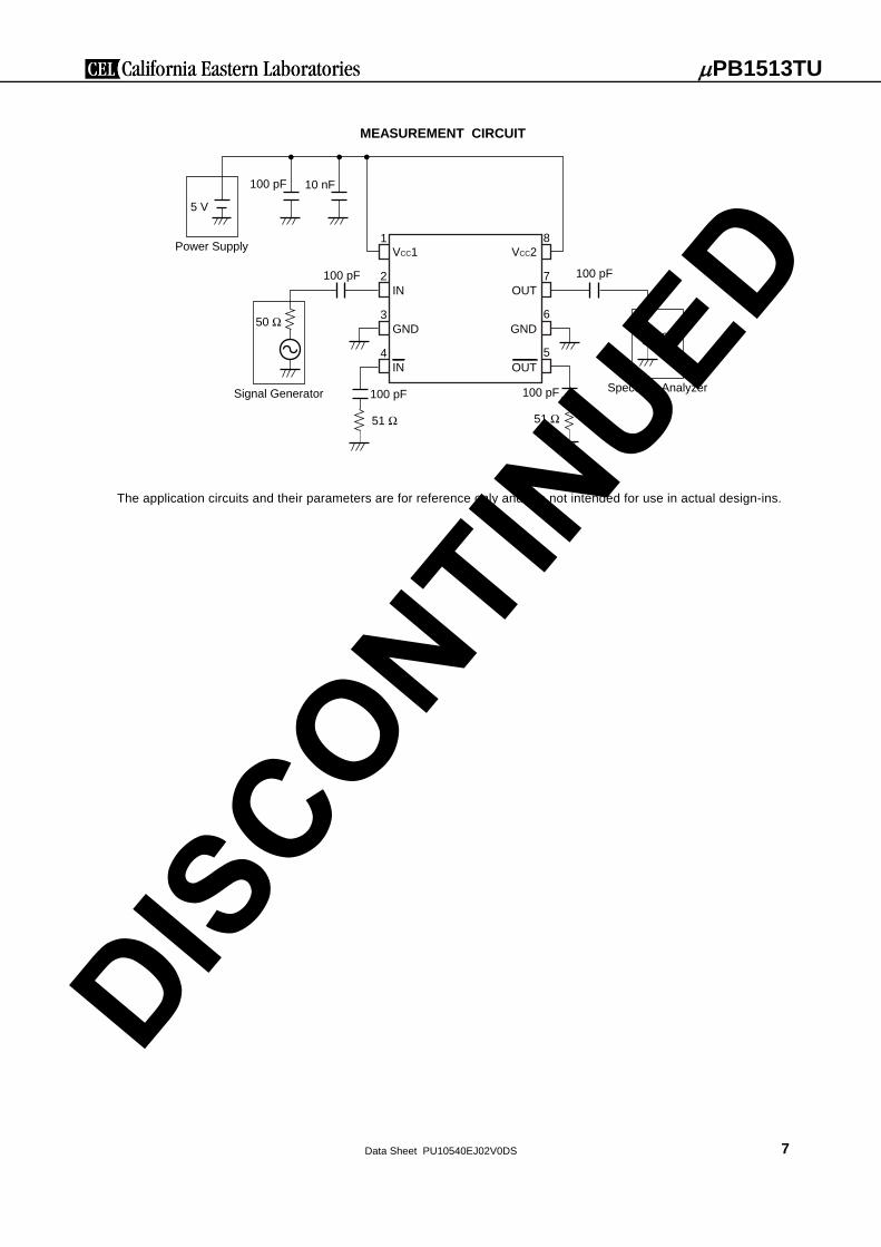
MEASUREMENT CIRCUIT
IN
GND
IN
VCC1
2
3
4
1
7
6
5
8
100 pF
50 Ω
Spectrum Analyzer100 pF
51 Ω
100 pF
51 Ω
100 pF
Signal Generator
50 Ω
OUT
GND
OUT
VCC2
5 V
Power Supply
100 pF 10 nF
The application circuits and their parameters are for reference only and are not intended for use in actual design-ins.
Data Sheet PU10540EJ02V0DS 7
DISCONTIN
UED

µPB1513TU
ILLUSTRATION OF THE MEASUREMENT CIRCUIT ASSEMBLED ON EVALUATION BOARD
51 Ω
51 Ω
100 pF
10 nF
100 pF
100 pF
100 pF
100 pF
1234
8765
Remarks 1. 33 × 21 × 0.4 mm double-sided copper-clad polyimide PCB 2. Back side: GND pattern 3. Solder plated on pattern 4. represents cutout 5. : Through holes
Data Sheet PU10540EJ02V0DS 8
DISCONTIN
UED

µPB1513TU
PACKAGE DIMENSIONS
8-PIN LEAD-LESS MINIMOLD (UNIT: mm)
1 2 3 4
8 7 6 5
2.2±
0.05
2.0±
0.1
(Top View)0.
5±0.
03
4 3 2 1
5 6 7 8
0.4±
0.1
0.4±
0.1
(1.4
)
(0.75)(0.75)
(0.25) (0.25)
0.16±0.05
(Bottom View)
2.0±0.1
(0.3
5)(0
.35)
(0.3
5)(0
.35)
(0.5
)(0
.5)
(0.6
)(0
.6)
(0.65)(0.65)
(0.6)
(0.3)
0.12
5+0.
1
–0.0
5
Data Sheet PU10540EJ02V0DS 9
DISCONTIN
UED
µPB1513TU
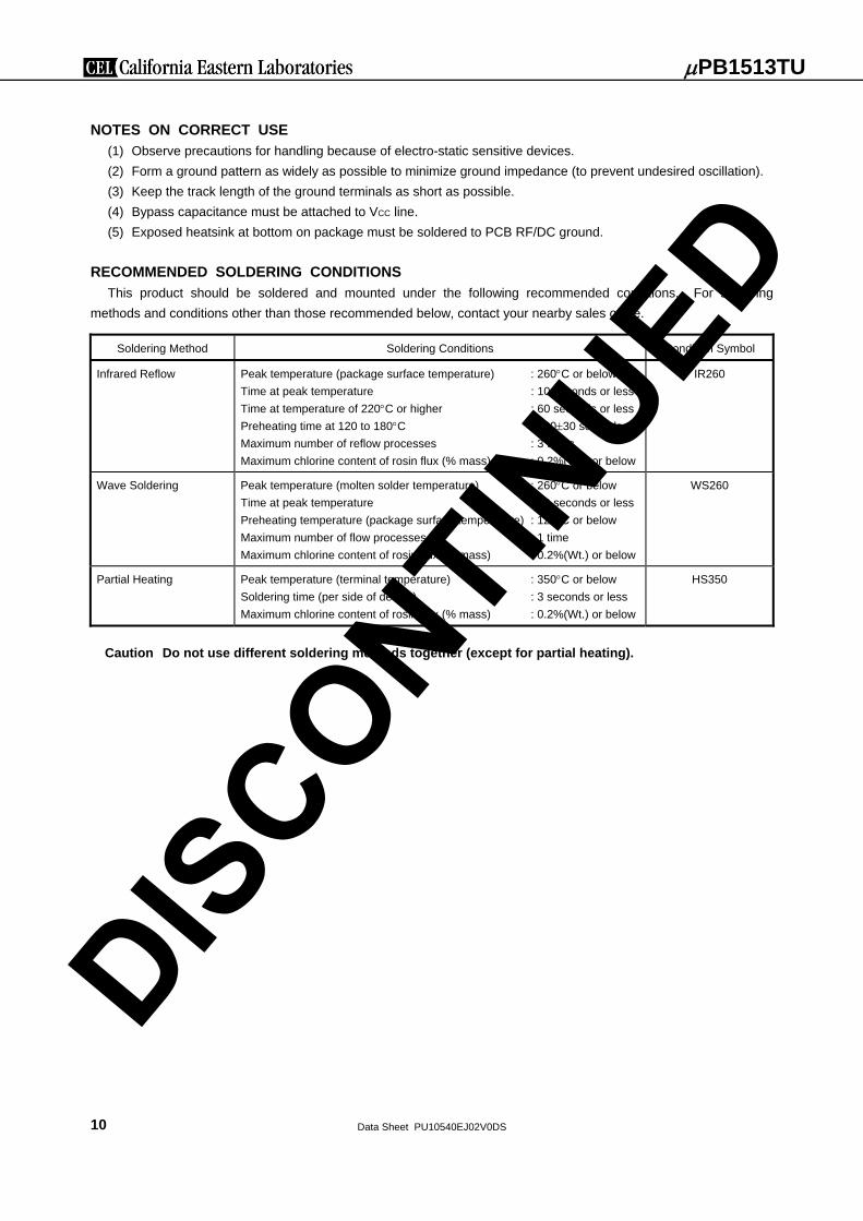
NOTES ON CORRECT USE (1) Observe precautions for handling because of electro-static sensitive devices. (2) Form a ground pattern as widely as possible to minimize ground impedance (to prevent undesired oscillation). (3) Keep the track length of the ground terminals as short as possible. (4) Bypass capacitance must be attached to VCC line. (5) Exposed heatsink at bottom on package must be soldered to PCB RF/DC ground.
RECOMMENDED SOLDERING CONDITIONS This product should be soldered and mounted under the following recommended conditions. For soldering
methods and conditions other than those recommended below, contact your nearby sales office.
Soldering Method Soldering Conditions Condition Symbol
Infrared Reflow Peak temperature (package surface temperature) : 260°C or below Time at peak temperature : 10 seconds or less Time at temperature of 220°C or higher : 60 seconds or less Preheating time at 120 to 180°C : 120±30 seconds Maximum number of reflow processes : 3 times Maximum chlorine content of rosin flux (% mass) : 0.2%(Wt.) or below
IR260
Wave Soldering Peak temperature (molten solder temperature) : 260°C or below Time at peak temperature : 10 seconds or less Preheating temperature (package surface temperature) : 120°C or below Maximum number of flow processes : 1 time Maximum chlorine content of rosin flux (% mass) : 0.2%(Wt.) or below
WS260
Partial Heating Peak temperature (terminal temperature) : 350°C or below Soldering time (per side of device) : 3 seconds or less Maximum chlorine content of rosin flux (% mass) : 0.2%(Wt.) or below
HS350
Caution Do not use different soldering methods together (except for partial heating).
Data Sheet PU10540EJ02V0DS 10
DISCONTIN
UED
µPB1513TU
When the product(s) listed in this document is subject to any applicable import or export control laws and regulation of the authorityhaving competent jurisdiction, such product(s) shall not be imported or exported without obtaining the import or export license.
M8E 00. 4 - 0110
The information in this document is current as of March, 2005. The information is subject to change without notice. For actual design-in, refer to the latest publications of NEC's data sheets or data books, etc., for the most up-to-date specifications of NEC semiconductor products. Not all products and/or types are available in every country. Please check with an NEC sales representative for availability and additional information.No part of this document may be copied or reproduced in any form or by any means without prior written consent of NEC. NEC assumes no responsibility for any errors that may appear in this document.NEC does not assume any liability for infringement of patents, copyrights or other intellectual property rights of third parties by or arising from the use of NEC semiconductor products listed in this document or any other liability arising from the use of such products. No license, express, implied or otherwise, is granted under any patents, copyrights or other intellectual property rights of NEC or others.Descriptions of circuits, software and other related information in this document are provided for illustrative purposes in semiconductor product operation and application examples. The incorporation of these circuits, software and information in the design of customer's equipment shall be done under the full responsibility of customer. NEC assumes no responsibility for any losses incurred by customers or third parties arising from the use of these circuits, software and information.While NEC endeavours to enhance the quality, reliability and safety of NEC semiconductor products, customers agree and acknowledge that the possibility of defects thereof cannot be eliminated entirely. To minimize risks of damage to property or injury (including death) to persons arising from defects in NEC semiconductor products, customers must incorporate sufficient safety measures in their design, such as redundancy, fire-containment, and anti-failure features.NEC semiconductor products are classified into the following three quality grades:"Standard", "Special" and "Specific". The "Specific" quality grade applies only to semiconductor products developed based on a customer-designated "quality assurance program" for a specific application. The recommended applications of a semiconductor product depend on its quality grade, as indicated below. Customers must check the quality grade of each semiconductor product before using it in a particular application. "Standard": Computers, office equipment, communications equipment, test and measurement equipment, audio
and visual equipment, home electronic appliances, machine tools, personal electronic equipmentand industrial robots
"Special": Transportation equipment (automobiles, trains, ships, etc.), traffic control systems, anti-disastersystems, anti-crime systems, safety equipment and medical equipment (not specifically designedfor life support)
"Specific": Aircraft, aerospace equipment, submersible repeaters, nuclear reactor control systems, lifesupport systems and medical equipment for life support, etc.
The quality grade of NEC semiconductor products is "Standard" unless otherwise expressly specified in NEC's data sheets or data books, etc. If customers wish to use NEC semiconductor products in applications not intended by NEC, they must contact an NEC sales representative in advance to determine NEC's willingness to support a given application.(Note)(1) "NEC" as used in this statement means NEC Corporation, NEC Compound Semiconductor Devices, Ltd.
and also includes its majority-owned subsidiaries.(2) "NEC semiconductor products" means any semiconductor product developed or manufactured by or for
NEC (as defined above).
•
•
•
•
•
•
Data Sheet PU10540EJ02V0DS 11
DISCONTIN
UED

µPB1513TU
NEC Compound Semiconductor Devices Hong Kong Limited E-mail: [email protected] (sales, technical and general) Hong Kong Head Office Taipei Branch Office Korea Branch Office
TEL: +852-3107-7303TEL: +886-2-8712-0478TEL: +82-2-558-2120
FAX: +852-3107-7309 FAX: +886-2-2545-3859FAX: +82-2-558-5209
NEC Electronics (Europe) GmbH http://www.ee.nec.de/ TEL: +49-211-6503-0 FAX: +49-211-6503-1327
California Eastern Laboratories, Inc. http://www.cel.com/ TEL: +1-408-988-3500 FAX: +1-408-988-0279 0406
NEC Compound Semiconductor Devices, Ltd. http://www.ncsd.necel.com/ E-mail: [email protected] (sales and general) [email protected] (technical) Sales Division TEL: +81-44-435-1588 FAX: +81-44-435-1579
For further information, please contact
DISCONTIN
UED
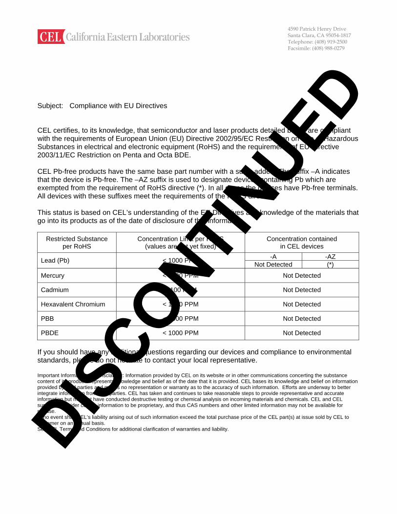
Subject: Compliance with EU Directives CEL certifies, to its knowledge, that semiconductor and laser products detailedwith the requirements of European Union (EU) Directive 2002/95/EC RestrictioSubstances in electrical and electronic equipment (RoHS) and the requiremen2003/11/EC Restriction on Penta and Octa BDE. CEL Pb-free products have the same base part number with a suffix added. Ththat the device is Pb-free. The –AZ suffix is used to designate devices containiexempted from the requirement of RoHS directive (*). In all cases the devices All devices with these suffixes meet the requirements of the RoHS directive. This status is based on CEL’s understanding of the EU Directives and knowledgo into its products as of the date of disclosure of this information.
Restricted Substance per RoHS
Concentration Limit per RoHS (values are not yet fixed)
Concein
-A Lead (Pb) < 1000 PPM Not Detect
Mercury < 1000 PPM N
Cadmium < 100 PPM N
Hexavalent Chromium < 1000 PPM N
PBB < 1000 PPM N
PBDE < 1000 PPM N
If you should have any additional questions regarding our devices and compliastandards, please do not hesitate to contact your local representative. Important Information and Disclaimer: Information provided by CEL on its website or in other communicationcontent of its products represents knowledge and belief as of the date that it is provided. CEL bases its knowprovided by third parties and makes no representation or warranty as to the accuracy of such information. Eintegrate information from third parties. CEL has taken and continues to take reasonable steps to provide reinformation but may not have conducted destructive testing or chemical analysis on incoming materials and suppliers consider certain information to be proprietary, and thus CAS numbers and other limited informationrelease. In no event shall CEL’s liability arising out of such information exceed the total purchase price of the CEL pacustomer on an annual basis. See CEL Terms and Conditions for additional clarification of warranties and liability. DIS
CONTINU
4590 Patrick Henry Drive Santa Clara, CA 95054-1817 Telephone: (408) 919-2500 Facsimile: (408) 988-0279
below are compliant n on Use of Hazardous ts of EU Directive
e suffix –A indicates ng Pb which are have Pb-free terminals.
ge of the materials that
ntration contained CEL devices
-AZ ed (*)
ot Detected
ot Detected
ot Detected
ot Detected
ot Detected
nce to environmental
s concerting the substance ledge and belief on information fforts are underway to better presentative and accurate chemicals. CEL and CEL may not be available for
rt(s) at issue sold by CEL to
ED