biosensors and bioelectronics - university of glasgow · different groups have worked on magnetic...
TRANSCRIPT

Contents lists available at ScienceDirect
Biosensors and Bioelectronics
journal homepage: www.elsevier.com/locate/bios
Magnetic biosensors: Modelling and simulation
Vahid Nabaeia, Rona Chandrawatib, Hadi Heidaria,⁎
aMicroelectronics Lab, School of Engineering, University of Glasgow, Glasgow G12 8QQ, UKb School of Chemical and Biomolecular Engineering, The University of Sydney, Sydney, NSW 2006, Australia
A R T I C L E I N F O
Keywords:Magnetic sensorsModellingSimulationHall sensorsGiant magnetoresistors
A B S T R A C T
In the past few years, magnetoelectronics has emerged as a promising new platform technology in variousbiosensors for detection, identification, localisation and manipulation of a wide spectrum of biological, physicaland chemical agents. The methods are based on the exposure of the magnetic field of a magnetically labelledbiomolecule interacting with a complementary biomolecule bound to a magnetic field sensor. This Reviewpresents various schemes of magnetic biosensor techniques from both simulation and modelling as well asanalytical and numerical analysis points of view, and the performance variations under magnetic fields at steadyand nonstationary states. This is followed by magnetic sensors modelling and simulations using advancedMultiphysics modelling software (e.g. Finite Element Method (FEM) etc.) and home-made developed tools.Furthermore, outlook and future directions of modelling and simulations of magnetic biosensors in differenttechnologies and materials are critically discussed.
1. Introduction
In recent years, an enormous surge of works has been carried out todevelop new methods for detection of a wide range of biomoleculartargets in life-science applications, medical diagnostics, and pharma-ceutical discovery. Development of high-speed, reliable, accurate andhigh-resolution biosensing platforms continues to be driven by the hugemarket potential for bio-detection systems (Blohm and Guiseppi-Elie,2001; Chin et al., 2007; Enserink, 2001; Prinz, 1998). Recent researchworks focusing on magnetic sensors and nanoparticles with applicationsin biomedicine and their detection by magnetic sensors underpin theseefforts. For example, magnetic nanoparticle based hyperthermia treat-ment, guided drug delivery and the use of magnetic particles as MRIcontrast agents are examples of highly successful research and clinicalmethods. Among the various biosensors, the magnetic biosensors haveattracted more attentions because of their remarkable advantages. Forexample, when compared to fluorescent based methods, magneticbiosensors have four advantages. First, magnetic probes are more stableover time in culture and can be used for long term labelling assays.Fluorescent tags are chemical compounds that can lose integrity as afunction of time; this is not the case with magnetic nanotags. Thisproperty can prove advantageous for long term labelling assays duringtissue and organ fabrication. Second, magnetic materials do not lead tobackground noise effects, which do occur with fluorescently labelledsamples. Background fluorescence is a common phenomenon in biolo-gical samples and is due to the inherent properties of the tissue. Third,
application of controlled magnetic fields on the external surface pro-vides a mechanism for remotely measuring and regulating the biolo-gical environment. And finally, the sensitivity of magnetic assays hasbeen shown to be greater than fluorescent assays. The high sensitivityallows detection at significantly lower protein concentrations, com-pared with fluorescent based techniques (Birla, 2016). Computer aidedmodelling and simulation towards optimal design of biosensing systemshas proven their feasible functionality and reliable performance(Nabaei, 2014). Simulation enables product comparison in a range ofcomplex physiological environments. Therefore, prototype fabricationcost will be decreased due to optimum design of the material and in-strument. However, computational modelling is not always a straight-forward approach and it is accompanying with major challenges thatmay hamper the development of new concepts. Despite considerableadvances in computing systems and methodologies in the last decade,modelling and simulation has not yet fully realized the potential andopportunities afforded by different technologies, and this has keptmodelling from achieving its fullest potential in modelling complex andvery large-scale systems.
Additional aspect is uncertainty. Models are necessarily approx-imate representations of real systems. There are always inherent un-certainties in the data used to create the model, as well as the beha-viours and processes defined within the model itself. It is critical tounderstand and manage these uncertainties in any modelling approach.Modelling of magnetic biosensing systems are not exceptional fromthese difficulties. A specific challenge in this area is the need to consider
https://doi.org/10.1016/j.bios.2017.12.023Received 4 November 2017; Accepted 16 December 2017
⁎ Corresponding author.E-mail address: [email protected] (H. Heidari).
Biosensors and Bioelectronics 103 (2018) 69–86
Available online 20 December 20170956-5663/ Crown Copyright © 2017 Published by Elsevier B.V. All rights reserved.
T

a wide array of relevant physical phenomena in the system. For in-stance, in the modelling of Hall sensor response to a localized magneticfield produced by a magnetic tip with bias voltage, a strong effect dueto capacitive coupling between the tip and the sensor arises (Heidariet al., 2015). This perturbing effect appears in the measurements and itshould be modelled to reach a more realistic and valuable simulationresult (Heidari et al., 2013; Nabaei et al., 2013). Another main chal-lenge is the scale of the system to be modelled and consequently the runtime of the simulation work. For example, in finite element method(FEM) based modelling for a good trade-off between accuracy and si-mulation run time, the meshed structures of the sample should containa sufficient number of points. Smaller meshing dimensions and highernumber of points increase the accuracy of the simulation results, butwould require more central processing unit (CPU) time and longer ex-ecution. One of the recent and effective techniques which have beenused to overcome to this problem is General-purpose computing on gra-phics processing units (GPGPU) that uses a GPU, which typically handlescomputation only for computer graphics, to perform computation inapplications traditionally handled by the CPU.
Different groups have worked on magnetic biosensors review, asinstance, one group has focused on magnetic impedance biosensors(Wang et al., 2017). They have first introduced the magnetoimpedanceeffect in some soft ferromagnetic devices, and then they have reviewedthe detection of magnetic ferrofluid, magnetic beads, magnetically la-belled bioanalytes and biomagnetic fields of living systems. Finally,some strategies have been proposed for design of the high-performancemagnetoimpedance biosensor, for quantitative and ultrasensitive de-tection of magnetically labelled biomolecules. Another team have re-viewed three types of biosensors including magnetic relaxation switchassay-sensors, which are based on the effects magnetic particles exerton water proton relaxation rates, magnetic particle relaxation sensors,which determine the relaxation of the magnetic moment within themagnetic particle, magnetoresistive sensors, which detect the presenceof magnetic particles on the surface of electronic devices (Sagadevanand Periasamy, 2014). Nano-scaled biosensors trends and their appli-cations have been reviewed in another work (Koh and Josephson,2009). In this study, the attention has been mainly focused on nanos-tructured materials, nano-particles, carbon nanotubes, and biologicalnanomaterial based biosensing devices.
This review presents an overview of magnetic biosensor modellingand simulation which have been developed in the past 10 years, fo-cusing on their mathematical models and solution methodology (suchas analytical and numerical). The applied model's strengths and
weaknesses are highlighted and the used competence of differentmodelling software, including commercial (i.e. Multiphysics modellingsoftware) and home-made, are discussed. The objectives of this surveypaper on magnetic biosensor modelling are threefold: (1) to addresseffective and competent magnetic biosensor modelling approaches; (2)to discuss challenges and difficulties in this area and propose possiblesolutions to overcome these challenges, (3) to introduce performedexperimental works on magnetic biosensor which have not applied anymodel, and propose modelling and simulation studies that can be de-veloped to enhance understanding and interpretation of the obtainedresults and optimization of the system.
2. Magnetic biosensors
This section reviews various representative low-magnetic fieldsensors and presents a brief overview of the different techniques andmechanisms as well as major results obtained so far in the developmentand application of these sensors.
2.1. Magnetoresistance device
In 1857, William Thomson (Lord Kelvin) first reported the aniso-tropic magnetoresistance (AMR) effect, observing that when iron wassubjected to a magnetic field there was a 0.033% increase in its elec-trical resistance (Thomson, 1856). This very subtle effect is the result ofthe variation of electron mean free path as a function of the angle of theelectron velocity with respect to material magnetization. The sensitivityof magnetoresistive (MR) materials is expressed as the change in re-sistance divided by the minimum resistance (MR ratio) (Fig. 1).
2.2. Giant magnetoresistance coupled multilayer
The giant magnetoresistance (GMR) effect happens in a multi-layerstructure in which magnetic and non-magnetic thin films are depositedalternately. When there is no external magnetic field, the magnetizationof all ferromagnetic layers is coupled to their neighbours oppositely. Atthis state, electron spins with both orientations are in low conductancespin channels due to the spin collision at the interfaces between fer-romagnetic and non-magnetic layers. This state is called the high re-sistance state (Fig. 2A). When we apply an external magnetic field, allthe ferromagnetic layer's magnetization is saturated in the field direc-tion. At this state, the electron spins with the orientation in the samedirection as the external magnetic field do not have spin collisions at
Fig. 1. Graphical overview of this review.
V. Nabaei et al. Biosensors and Bioelectronics 103 (2018) 69–86
70

the interfaces, thus they are in a high conductance spin channel. Thisstate is called the low resistance state (Fig. 2B and C).
Since the GMR systems are able to sense very low magnetic fields,the potential of GMR for magnetic bead detection was realized and ledto development of magnetic biosensor for life science applications.GMR effect was first described independently by Baibich et al. (1988)and Binasch et al. (1989) through the study of magnetic properties ofmagnetic and nonmagnetic metal thin film multilayers. Baselt et al.(1998) described a new concept in biological labelling and magneticsensor detection based on GMR sensors.
They introduced a semiconductor-based multilayer GMR sensorchip, which came to be known as the bead array counter chip thatdetects local in-plane magnetic fields produced by paramagnetic mi-crobeads immobilized directly above the sensor surface during anti-body–antigen binding assays. Other investigators have also followedBaselt's initial approach with other GMR sensor devices (Reiss et al.,2005; Schotter et al., 2002, 2004). The principle detection is shown inFig. 2D and E. Specific antigens are immobilized on the sensor surface.Superparamagnetic nanoparticles or beads, which are specifically at-tached to a target antibody, are used for detection. In a washing step,unbound magnetic beads are removed and beads bound to antigenmolecules are measured. The superparamagnetic nature of the beads
allows to switch on their magnetic stray field by a homogeneous ex-ternal magnetic field oriented perpendicular to the sensor surface(Fig. 2E). Hence, the stray field components of the magnetic markerswithin the sensitive sensor area can be detected by a drop in the elec-trical resistance of the GMR sensor. For an optimum bead detection,GMR sensors with isotropic signals and high sensitivities are needed.
Li et al. (2010) developed a GMR system that can detect interleukin-6 (IL-6), a potential cancer biomarker, in unprocessed human serum.The GMR sensor was first functionalized with capture antibodies. In thepresence of IL-6, a sandwich with detection antibodies labelled mag-netic nanoparticles was formed. Subsequently, dipole field generated bythe particles captured on the sensor surface was detected. This methodoffers IL-6 detection down to 125 fM within 5 min. The assay only re-quires 4 μL of serum sample for analysis, and the near 0° magnetizationdesign of the GMR sensor eliminates the need for a high magnetic field.Collectively, this system has a great potential for a point-of-care device.
Some more recent works have also demonstrated that the GMRsensors are promising candidates for biomedical applications (Ennenet al., 2016; Rizzi et al., 2017; Xu et al., 2016). A CMOS front-end withintegrated magnetoresistive sensors for biomolecular recognition de-tection applications have been reported (Costa et al., 2017). Char-acterization of the GMR sensor's signal and noise has shown CMOS
Fig. 2. (A) Schematic diagram of a current in plane GMR structure: magnetization of all ferromagnetic layers is coupled oppositely (high resistance state). (B) and (C) magnetization of allferromagnetic layers are saturated in one direction by an external field (low resistance states). Schematic representation of a magnetic biosensor: (D) a superparamagnetic beadfunctionalized with a receptor molecule hybridize to the target molecule attached onto the sensor surface; (E) An external field align the magnetic moment of the bead and the magneticstray field can be detected by the GMR sensor (Binasch et al., 1989). Schematic diagram of the spin-valve structure and operation of current perpendicular to the plane of GMR spin-valveat (F) parallel (low resistance) state and (G) antiparallel (high resistance) state. (H) Simulations and measured MR response of PSV ring. Micromagnetic simulations (using OOMMF) showmagnetization states of a 2 μ m PSV ring with 200 nm line width as the Py layer is cycled from reverse onion (H1) to forward onion state (H2) and back, as indicated by the arrows. MRmeasurements on an actual microfabricated ring confirm that the reverse onion state of the Co layer remains largely undisturbed during the cycling, giving rise to minimum (H1) andmaximum (H2) MR levels. The plateaus correspond to vortex states (H3) in the Py layer obtained on the ascending and descending field sweeps (Corte-León et al., 2014). Results of beaddetection: (J) Schematic showing the induced dipole field from a single magnetic bead partially cancelling the externally applied field over the ring. (K) Minor hysteresis loops of the 4 µmPSV ring taken in both presence (red open circles) and absence (black solid squares) of the bead after saturating the ring at −1500 Oe (Corte-León et al., 2014). Reprinted withpermissions. (For interpretation of the references to color in this figure legend, the reader is referred to the web version of this article).
V. Nabaei et al. Biosensors and Bioelectronics 103 (2018) 69–86
71

building blocks were designed targeting a negligible noise when com-pared with the GMR sensor's noise and a low power consumption. TheCMOS front-end was fabricated using the magnetoresistive sensors werepost-fabricated on top of the CMOS chip with high yield. Due to its lowcircuit noise and overall equivalent magnetic noise, the full system wasable to detect 250 nm magnetic nanoparticles with a circuit imposedsignal-to-noise ratio degradation of only−1.4 dB. Furthermore, the lowpower consumption (6.5 mW) and small dimensions (7.59 mm2) of thepresented solution guarantees the portability of the detection systemallowing its usage at the point-of-care. A simple and sensitive methodfor the detection of influenza A virus based on giant magnetoresistance(GMR) biosensor has been developed in another work (Krishna et al.,2016). Authors have demonstrated GMR biosensor detected as low as1.5 × 102 TCID50/mL virus and the signal intensity increased withincreasing concentration of virus up to 1.0 × 10⁵ TCID50/mL. Thisstudy has shown that the GMR biosensor assay is relevant for diagnosticapplication since the virus concentration in nasal samples of influenzavirus infected swine was reported to be in the range of 103 to 105TCID50/mL. Another group systematically investigated time-domainMagnetorelaxometry (MRX) by measuring the signal dependence on theapplied field, magnetization time, and magnetic core size (Huang et al.,2017). MRX is a promising new biosensing technique for point-of-carediagnostics. The extracted characteristic times varied for differentmagnetic nano-particles (MNPs), exhibiting unique magnetic sig-natures. The signal contribution based on the MNP location and cor-related the coverage with measured signal amplitude has been alsomeasured. Lastly, the authors demonstrated, for the first time, a GMR-based time-domain MRX bioassay. This approach validates the feasi-bility of immunoassays using GMR-based MRX and provides an alter-native platform for point-of-care diagnostics.
2.3. Spin valves
Another type of GMR effect occurs when the current is perpendi-cular to the film plane. This forms the basis of the so-called GMR spin-valve, which was first described by Dieny et al. (1991) It normallycontains three main layers. A pinned layer, whose magnetization doesnot change with the external field, is normally pinned by an anti-ferromagnetic substrate, and a free layer works as a switch of the spin-valve (Fig. 2F and G). The magnetic materials could be Ni, Co and Fe. Anon-magnetic conducting layer such as Cr, Cu, Ru, or Ag separates thepinned and free layers (Baibich et al., 1988; Pratt et al., 1991). Whenthe free layer is parallel to the pinned layer the electrons, whose spinshave the same orientation with the layers travel in a wide spin channelwhereas the oppositely oriented electron spins have a narrow channel.When the two layers are antiparallel, electron spins in either orientationhave a narrow channel in the layer with the opposite magnetization.Therefore, the resistance of a parallel state is smaller than the anti-parallel state.
This device has been used for magnetically-labelled biosensorsby Graham et al. (2005, 2004) and Li et al. (2003b, 2006). Grahamet al. described a 2 µm × 6 µm sensor consisting of a MR material stackwith two ferromagnetic layers, typically a NiFe-based composite, whichare separated by a Cu spacer to detect bulk numbers of 400 nm dextraniron oxide particles. Recent research revealed that a graphene layer canbe used as the separation layer for a GMR spin-valve (Munoz-Rojaset al., 2009). Llandro et al. (2007) have presented a magnetic multi-plexed assay technology which encodes the identities of target biomo-lecules according to the moment of magnetic beads to which they areattached. They have shown that pseudo spin valve ring can detect asingle sized-matched bead in a digital manner. Simulations (using Ob-ject Oriented Micro Magnetic Framework (OOMMF) software) of themagnetization states of a Py (4 nm)/Cu (5 nm)/Co (7 nm) ring with2 µm outer diameter and 200 nm line width and an exemplar minor MRloop of the same structure are shown in Fig. 2H. An external magneticbead is applied to a bead placed over the ring. Since the bead
magnetization aligns with applied field, the stray field thus generatedopposes and partially cancels the applied field bellow the bead (sche-matically shown in Fig. 2J). Fig. 2K shows minor MR loops taken with(red open circles) and without (black solid squares) bead over the ring.The shifts of the permally layer transition due to the dipole field gen-erated from the bead can clearly be seen.
2.4. Magnetic tunnel junctions
Tunnelling magnetoresistance (TMR) is similar to GMR but has anon-magnetic insulating layer instead of a conducting one. The in-sulating layer is normally 1–2 nm thick, such that the electrons cantunnel through. These sensors are also known as magnetic tunneljunctions (MTJ). The materials of the insulating layer could be Al2O3
(Moodera et al., 1995), Ga2O3 (Li et al., 2000), MgO (Khan et al., 2008),and graphene (Cobas et al., 2012). TMR were first demonstrated in-dependently by Moodera et al. and Miyazaki and Tezuka (Cobas et al.,2012; Khan et al., 2008; Li et al., 2000; Miyazaki and Tezuka, 1995;Moodera et al., 1995). Several groups have demonstrated the capabilityof TMR sensors to detect micro to nano-sized magnetic beads (Brzeskaet al., 2004; Shen et al., 2005; Wang et al., 2005). MTJs are the mostsensitive magnetoresistance sensors with a MR ratio of 20–50%, or, asmore recently reported, over 200% when using a MgO tunnel barrier(Parkin et al., 2004b). Instead of a Cu spacer like that found in the spin-valve construction, MTJs have a thin insulating layer (≤ 2 nm thick),which acts as a tunnel barrier. The thickness of the insulating layer canbe varied to effectively “tune” the device sensitivity. Additionally, thesensing current is directed perpendicular to the relatively large areaMTJ layers rather than in the plane of the sensor as used in GMRstructures. Wang et al. (2005) are pursuing this concept to produce a106 sensor array, with the promise of each sensor detecting a singlemagnetic label attached to a single DNA fragment. In a study by Albonet al. (2009) arrays of tunnel magnetoresistance sensors have beenemployed to detect magnetic microbeads. For single bead detection,elliptically shaped sensors of axis lengths of 400 and 100 nm are used. Alinear response of the sensor signal in a magnetic field range between−500 and +500 Oe has been reported. An elliptical element with alength of 400 nm on the longitudinal and 100 nm on the transverse axishas been used (Fig. 3A). Magnetic markers 1 µm Dynabead® MyOne™are used, which are superparamagnetic and consist of about 8 nm ma-ghemite magnetic nanoparticles embedded in a porous polymer matrix.Detection of the magnetic labels is done by applying an in-plane dcmagnetic field over the linear range of the sensor. The external mag-netic field is chosen parallel to the y axis (as indicated in Fig. 3B). Sincethe sensitivity varies between each sensor, they have introduced therelative resistance change
∆ =−TMR R R
Rbea sensor
sensor
d
(1)
where Rbead and Rsensor denote the resistance of the TMR sensor with andwithout bead, respectively. The obtained signal depends on the positionof the bead with respect to the sensor (Fig. 3C). The noise signal hasbeen evaluated by subtracting the sensor resistances between twoconsecutive measurements done before coating the sensor surfaces withbeads. In general, for parallel orientation of the magnetization in thepinned layer and the external homogenous field, we find an increasingsensor resistance if the particle is placed along the long axis of the el-lipse and a decreasing resistance value if it is located along the shortaxis.
2.5. Anisotropic magnetoresistance (AMR) based devices
The anisotropic magnetoresistance (AMR) effect leads to a localdependence of electrical conductivity on the mutual orientation ofmagnetization and current density vectors. The ferromagnetic sampleshows high resistivity when the magnetization direction is parallel to
V. Nabaei et al. Biosensors and Bioelectronics 103 (2018) 69–86
72

the current, and low resistivity when they are perpendicular (Beguivinet al., 2014; Corte-León et al., 2014; Manzin et al., 2014). Before GMR,there was an active pursuit of devices utilizing AMR (Mcguire andPotter, 1975). Miller et al. (2002) introduced the use of AMR tech-nology in the form of a ring sensor. In the ring approach, a single-layer,current-in-plane Ni80Fe20 ring sensing element is fabricated wherebythe AMR material is modulated by the radial fringing field from a singlemagnetic bead. The ring sensor has outer and inner diameters of 5 µmand 3.2 µm, respectively. When the bead is centred over the ring, theradial fringing field rotates the magnetization from circumferentialtowards a radial outward direction. This rotation causes a magnetore-sistance to decrease and a measurable voltage signal in the Wheatstonebridge. Recently, AMR nanostructures with different shapes such as L-shape (Donolato et al., 2009), square ring (Vavassori et al., 2008), andzigzag (Donolato et al., 2010; Ruan et al., 2010; Vieira et al., 2012,2009) have been employed for detection of magnetic beads. Donolatoet al. (2009) have presented a device concept based on controlled mi-cromagnetic configurations in a corner-shaped permalloy nanostructureterminated with two circular disks (Fig. 3D). The device consists of apatterned L-shaped permalloy strip, 25 nm thick and 180 nm wide, withtwo end disks (diameter 500 nm) that have their centre at 2 µm fromthe corner. They have performed AMR measurements on the studieddevice and it can be seen from Fig. 3H the beads grouped on the cornerby the domain wall (DW) can influence the position of the first tran-sition (for positive magnetic field) corresponding to the removal of thedomain wall from the corner where the beads are located. Magneticbead detection using DW-based magnetic nanostructures (e.g. a L-shaped nanowire) and based on AMR properties of the nanostructurehas two main steps; first step is pinning of the DW in the nanostructure(corner), the second step is characterization of the AMR properties ofthe nanostructure in the presence and absence of the magnetic bead
grouped by the DW on the corner of the nanostructure.
2.6. Hall magnetometry
Hall sensors are versatile devices exhibiting a high magnetic mo-ment sensitivity over a wide field range and an elevated signal-to-noiseratio in both low and room temperature conditions (Heidari et al.,2014, 2016). Moreover, they generally provide a linear response, beingnot affected by magnetic saturation. These sensors have been studiedand investigated both experimentally and numerically for differentapplications, such as Hall magnetometry on nanostructures, detectionof magnetic beads as label in medical application.
2.7. Hall devices for detection of magnetic beads
As one of the most important applications, Hall sensors have beenadopted for the detection (Besse et al., 2002; Di Michele et al., 2011;Haun et al., 2010; Kazakova et al., 2007; Landry et al., 2004; Llandroet al., 2010; Manandhar et al., 2009; Mihajlovic et al., 2007, 2005;Sandhu et al., 2007) and even counting (Lee et al., 2009) of individualmagnetic nanobeads used as labels for medical imaging, drug deliveryand manipulation of biological species (Gijs, 2004; Pankhurst et al.,2003). Furthermore, they can be used to map the trajectory of movingbeads, as demonstrated by Aledealat et al. (2010) for the dynamic de-tection of superparamagnetic beads in a microfluidic channel integratedwith an InAs quantum well micro-Hall sensor. As one of the pioneeringgroups, Besse et al. have used a cross-shaped silicon Hall sensor fabri-cated in CMOS technology with active area 2.4 × 2.4 µm2 for the de-tection of a single magnetic bead (Dynabead M-280) (Besse et al.,2002). Mihajlović et al. (2005) have performed a room-temperaturedetection of a single commercial superparamagnetic bead suitable for
Fig. 3. (A) Sensor setup and initial magnetization of the ferromagnetic electrodes (Donolato et al., 2010). (B) The in-plane magnetic field of a bead with magnetic moment of 67.2 kA/maligned parallel to the y axis. The black lines indicate the component value Hy = 0. (C) Examples of the detection of single superparamagnetic beads with respect to its orientation towardthe sensor. Insets show the experimental situation (Donolato et al., 2010). (D) 3D schematic of the device interacting with a magnetized particle (Enserink, 2001). (E) AFM image of aclean device. (F) and (G) AFM images after the first and second dispensation of a drop of the same volume (2 μL) and concentration of beads (5 × 10¹⁰ particles mL−1). (H) Voltage dropacross the corner as a function of the magnetic field for the clean ring (squares), with the cluster of beads of panels (c) (triangles) and (d) (circles). The field is applied starting from 0 Oeand cycled back and forth up to±280 Oe (Enserink, 2001). Reprinted with permissions.
V. Nabaei et al. Biosensors and Bioelectronics 103 (2018) 69–86
73

biological applications, using an InAs quantum-well micro-Hall sensor.Their studies have demonstrated the use of phase-sensitive detection ona single Hall cross as well as in a Hall gradiometry setup. Sensor geo-metry and test result of ac phase sensitive detection are shown inFig. 4A and B, respectively. A clear drop in the Hall voltage is observedfor the cross with the bead and it is completely absenting for the emptycross. The magnitude of the voltage decrease is 2.0 µV, which corre-sponds to a change in the sensed stray field of 80 µT (Fig. 5).
Kazakova et al. have also presented detection and susceptibilitymeasurement experiments on a single superparamagnetic bead
applying an ac-dc measurement technique (Di Michele et al., 2011,2010; Kazakova et al., 2010). The detection and magnetic character-ization of the bead were performed using ultra-sensitive InSb Hall de-vices. Single bead detection was demonstrated using a step-wise changeof the dc magnetic field; measurements were performed using only thein-phase component of the total ac Hall voltage. Very clear evidence ofthe bead presence was simultaneously demonstrated with explicit se-paration of parasitic inductive signals (Fig. 4C and D).
The Hall sensors have also been employed for the counting ofmagnetic beads by Lee et al. (2009). For this purpose, Hall resistances
Fig. 4. (A) SEM image of two adjacent Hall crosses adapted toshow the actual detection measurement configuration; (B) ac Hallvoltage as a function of time for the two crosses shown in part (A)of the figure. The drop in the signal from one cross upon applyingthe static field B1 is due to the presence of the bead (Grahamet al., 2004). In-phase (Vx) and out-of-phase (Vy) components ofthe ac Hall voltage in response to BDC steps (BDC = 100 mT) witha duration of 30 s as measured on (C) an empty device and (D) adevice with a Dynal bead. Note that the Vy component alwaysshows an increase of the voltage independent of the presence ofthe bead. The effect is associated with dominating inductive andparasitic ferromagnetic signals. The gray rectangles represent thestate when BDC is on Issadore et al. (2013). Experimental (fullsquares) and calculated (open circles) Hall resistance at H = 0 asa function of the number of beads. The solid lines are guides forthe eyes. (E) and (F) are for the Hall sensors that are 9.3 µm and20 µm in width, respectively. The inset of (E) illustrates an ex-ample of lattice points in the sensor area for calculation, where wis the width of the Hall sensor and d is 2.8 µm, i.e., the diameter ofa bead. The calculated values are an average, and the upper andlower error bars indicate the maximum and minimum values,respectively (Kazakova et al., 2007). Hall voltage loops of Per-malloy disks (diameter: 800 nm, thickness: 30 nm, temperature:1.4 K) containing three and four artificial pinning centres. Thefield is applied in the plane of the disks as indicated by arrows.(G) The three branches of the minor loop reflect pinning of thevortex core at different pinning sites. The blue hysteresis branchcorresponds to pinning at the blue pinning site, etc. Double ar-rows represent reversible sections of the stray field curves, whilesingle arrows show the direction of irreversible jumps. The anti-dots were separated by 200 nm. (H) Four stable magnetic statescan be found in a disk with four antidots separated by a distanceof 150 nm. Switching from plateau (i) to (ii) is accomplished byapplying an external magnetic field between Hsw2 and Hsw3 (Liet al., 2000). Reprinted with permissions. (For interpretation ofthe references to color in this figure legend, the reader is referredto the web version of this article).
V. Nabaei et al. Biosensors and Bioelectronics 103 (2018) 69–86
74

measured at room temperature are found to be proportional to thenumber of the magnetic beads (Fig. 4E and F), and are in good agree-ment with the numerically simulated results presented in this study.Proposed sensors are designed to measure the number of beads betweenzero and full-scale signals for a given number range of interest.
A microfluidic chip-based micro-Hall (μHall) platform for sensitivedetection of bacteria was recently reported (Issadore et al., 2013). Inthis approach, target bacteria (Staphylococcus aureus) were magneticallylabelled using molecular ligands, rendering them superparamagnetic.The local magnetic fields produced by individual bacteria were thenmeasured by the μHall sensors. This system enables bacteria detection
within 1 h over a wide dynamic range (101–106 counts) and the authorsdemonstrated the ability to distinguish Gram-positive from Gram-ne-gative bacteria. By changing the molecular ligands, this assay could beadapted to differentiate a variety of other bacterial species.
2.8. Hall magnetometry on magnetic nanostructures
The magnetic behaviour of sub-micrometre ferromagnetic elementshas become increasingly important because of their application inmagnetoelectronic devices. These devices typically contain a patternedsoft magnetic layer which is switched between two magnetization states
Fig. 5. (A) Single bead detection experiment (Mihajlovic et al., 2005). (B) Influence of bead distance from sensor (Mihajlovic et al., 2005). (C) SEM image of an iron particle array grownonto Permalloy (where the particles with diameters of about 13 nm are arranged on a hexagonal lattice) and setup of the magnetic measurements (Miller et al., 2002). (D) Comparison ofcalculated (top) and measured (bottom) Magnetization reversal for a particle-Permalloy heterostructure. The calculated total magnetization of the particles, Ip and its derivative dIp /dHshow clearly a reversal in two steps. The measured Hall voltage can favourably be compared to dIp/dH. Again, a sharp and a broader step due to the particles’ influence can be recognized(Miller et al., 2002). (E) Coordinate system used in the calculations, and simulation results (Miyazaki and Tezuka, 1995): (F) Perpendicular component of the magnetic field from amagnetic bead in a direction perpendicular to the sensor plane, (G) magnetic field detected by the Hall sensor as a function of bead position, (H) perpendicular component of magneticfield from a magnetic bead in a direction horizontal to the sensor plane, and (I) magnetic field detected by the Hall sensor as a function of bead position (Miyazaki and Tezuka, 1995).Reprinted with permissions.
V. Nabaei et al. Biosensors and Bioelectronics 103 (2018) 69–86
75

(Manzin and Nabaei, 2014). Micro and nanostructured permalloymedia are a possible candidate for such devices (Gallagher et al., 1997;Gomez et al., 1999; Kirk et al., 1997). In particular, with circular na-nomagnets made of permalloy or cobalt, it might be possible to realizethe needed micromagnetic characteristics (Cowburn et al., 1999;Guslienko et al., 2002; Prejbeanu et al., 2002; Pulwey et al., 2001;Raabe et al., 2000; Schneider et al.al., 2002, 2000). Hall-magnetometry,imposing a negligible perturbation on the nanomagnet during themagnetization reversal process, has been introduced as a powerful toolfor the detection of nanostructure stray field. An important advantageof this method is that it can be employed over a wide range of tem-peratures, i.e. from cryogenic temperatures up to ambient temperature.This technique has been used by different groups to measure stray fieldhysteresis loops of different nanostructures (Hengstmann et al., 2001;Rahm et al., 2003a, 2003b; Schneider et al., 2003; Schuh et al., 2001).Rahm et al. (2003b) have used Hall sensors fabricated from GaAs/Al-GaAs heterojunction material to measure stray field hysteresis loops ofindividual disks. Hall magnetometry on individual ferromagnetic diskshas also been performed to study vortex pinning at single point defects(Rahm et al., 2004a). As a main conclusion, the authors showed, byusing Hall magnetometry, that point defects inside ferromagnetic diskscan significantly alter the corresponding hysteresis trace. By means ofHall magnetometry, it has been also put in evidence that inserting nantidots (holes) into a disk the magnetization reversal takes place via(n-1) jumps of the vortex core between neighbouring antidots (Rahmet al., 2004b). The results of this study are shown in Fig. 4G and H. Itcan be seen from measurements that each defect represents an artificialpinning site for the magnetic vortex core. Besides experimental Hallmagnetometry on nanostructures, analytical studies also show that theintroduction of a hole into a ferromagnetic nanodisk may deeply modifythe structure and dynamics of a vortex like state (Moura-Melo et al.,2008)
2.9. Hall sensor response to local electric and magnetic fields
Scanning gate microscopy (SGM) is a technique that can be used toexplore magnetic sensitivity of Hall effect sensors. In this technique, themeasured quantity is the transverse Hall voltage of the device while themagnetic tip is scanned over the sensor surface. The magnetic tip,conventionally used for magnetic force microscopy, is here used as asource of stray magnetic field to be detected by Hall effect sensors(Nabaei et al., 2013). The magnetic tip can be also electrically chargedand thus capacitively coupled to the sensor plane, due to the applica-tion of a voltage bias or contamination phenomena, producing per-turbing electric fields. This phenomenon has been investigated throughnumerical modelling and experimental analysis in (Nabaei et al., 2013).Folks et al. have measured the room temperature response of nanoscale
semiconductor Hall crosses to local applied magnetic fields under var-ious local electric gate conditions using scanning gate microscopy. Inthis study, near-surface quantum wells of AlSb/InAs/AlSb, located just5 nm from the heterostructure surface, allow very high sensitivity tolocalized electric and magnetic fields applied near the device surfaces.The Hall crosses have critical dimensions of 400 and 100 nm. Withcertain small gate voltages (Vg) the devices of both sizes are stronglyresponsive to the local magnetic field at the centre of the cross. Theauthors have found that, at high Vg, the response to local magneticfields is greatly distorted by strong electric fields applied near the crosscorners (Folks et al., 2009). Baumgartner et al. (2006) have presentedscanning gate measurements on a Hall cross in the regime of the clas-sical Hall effect. The real-space patterns of induced resistance changesare manifestations of the symmetry properties of such a Hall system.The detailed behaviour in the diffusive regime has been shown to becompatible with models based on a local conductivity tensor. Hall crossgeometry sensor also have been used as a local electric field probe,which is capable of detecting an electric charge as small as the charge ofone electron, operating under ambient conditions and having a spatialresolution down to 100 nm (Barbolina et al., 2006). The submicron-sized probes were made from a high-density high-mobility two-di-mensional electron gas, which is sensitive to the presence of electriccharges near its surface. The authors demonstrate the possibility ofusing such microprobes for life-science applications by measuring anelectric response of individual yeast cells to abrupt changes in theirenvironment.
2.10. Superconducting quantum interference device (SQUID)
One of the most sensitive low field sensors is the superconductingquantum interference device (SQUID)(Tamanaha et al., 2008) devel-oped around 1962 with the help of Brian J. Josephson's work (Lenz,1990). Kotitz et al. (1997) first introduced the concept of SQUID todetect antibodies labelled magnetic nanoparticles as a way to avoidusing radioisotopes or unstable enzymes or fluorescent dyes that arestandard in immunoassays. Externally applied magnetic field magne-tizes the superparamagnetic nanoparticles such that they line up alongthe magnetic field lines. When the magnetic field is removed, the par-ticles remain aligned for a brief period before randomizing again. Thisshort, but decaying, period of self-magnetization is described as amagnetic remanence. A SQUID measures the decay of remnant mag-netization of superparamagnetic nanoparticles bound to targets. Inanother SQUID measurement technique, Enpuku et al. (2005) andTsukamoto et al. (2005) developed a 25 nm-diameter (nominal) Fe3O4
magnetic marker with a high magnetic field and designed an optimizedpickup coil to detect the magnetic flux signal from a moving sample.
Fig. 6. Various magnetoresistance effects. Reproduced fromTumanski (2001, 2016).
V. Nabaei et al. Biosensors and Bioelectronics 103 (2018) 69–86
76

3. Discussion
Among the various magnetoresistive effects (Fig. 6), AMR effect,GMR, spin valve effect and magnetic tunnel junction MTJ are com-monly being used (Tumanski, 2001). Despite the fact that the AMRsensors are treated as slightly old-fashioned sensors but they have in-teresting advantages. They are very cheap and still available. The AMRsensors have better sensitivity than GMR sensors. In these sensorspreparation of pairs of sensors to remove the influence of the tem-perature is easy. In contrary, the main disadvantages of AMR sensorsare relative small change of resistance, not exceeding 2% and possibi-lity of demagnetization by high magnetic field. The GMR sensors in twothin ferromagnetic films, transition from initial antiparallel to parallelstate is accompanying by a very large (even more than 100%) change ofresistance. The main disadvantage of classical GMR effect was puresensitivity. Antiparallel state was obtained by strong coupling of twolayers separated by very thin separator. The MTJ sensors with spacermade by oxidized aluminum have quite large magnetoresistance about40% for relative small magnetic field (Fig. 6). But this type of MTJ hadsome problems with noises and small polarization voltage. Another typeof MTJ with barrier of crystalline textured MgO has magnetoresistanceas large as 180–220% (Parkin et al., 2004a; Yuasa et al., 2004).
Hall effect devices with simple design and technology of manu-facturing are most widely used magnetic sensors. They are very cheapbut the sensors for magnetic field measurement with high linearity andsmall temperature errors are expensive. Other remarkable advantagesof these sensors are the lack of ferromagnetic elements and the possi-bility of measuring of the various parameters such as current, angle,radial and axial position. The offset voltage of a Hall device is a quasi-static output voltage that exists in the absence of a magnetic field. Itseverely limits the applicability of Hall sensors when non-periodic orlow frequency magnetic signals have to be detected. Relative low sen-sitivity and high consumption are the other drawbacks of these devices.It is important to note that using high mobility material for Hall sensorslead to high sensitivity and low offset. It should be also noted thatminiaturization of the hall sensors deteriorates their performance andthis deterioration can be compensated by the associated electroniccircuit, but this implies a rising of the development costs. The highestsensitivity exhibits SQUID sensors with noise about 5 fT/√ Hz enableto detect fTmagnetic field. Therefor they are suitable for magnetic fieldresulting from brain activity. The NDT techniques also profit this highsensitivity to detect and even to forecast defects (Krause andKreutzbruck, 2002). One of the drawbacks of the SQUID devices is thatthe application of this type of magnetic sensors is restricted to lowtemperature condition.
Magnetic sensors working range and a category of magnetic sensorsapplications are presented in Fig. 7 and Table 1 (Lenz and Edelstein,2006). As can be seen, magnetic sensors have a broad range of appli-cations. For example, ultra-sensitive magnetic sensors are able to detecttiny magnetic fields produced outside the brain by neuronal currents,
which can be used for diagnostic applications. High reliability non-contact switching with magnetic sensors leads to enhanced safetystandards in aircraft, and magnetic sensors are also used in automobilesto detect positions in the engine crank shaft and wheel braking. Com-puters have nearly unlimited memory through the application ofmagnetic sensors in magnetic storage hard drives and tape drives(Nazari Nejad, 2015).
4. Modelling and simulation of magnetic biosensors
4.1. Finite element modelling and methodology
There are a great many numerical techniques used in engineeringapplications for which digital computers are very useful. The numericaltechniques generally employ a method which discretizes the continuumof the structural system into a finite collection of points (or nodes)/elements called finite elements. The most popular technique used cur-rently is the finite element method (FEM). There are other methods likethe finite difference method (FDM) and the boundary element method(BEM).
4.2. Finite element method
In the finite element method (FEM) of analysis a complex regiondefining a continuum is discretized into simple geometric shapes calledfinite elements. The material properties and the governing relationshipsare considered over these elements and expressed in terms of unknownvalues at elements corners. An assembly process duly considering theloading and constraints results in a set of equations. Solution of theseequations gives the approximate behaviour of the continuum. The basicsteps in the FEM are: (1) Discretization of the domain; (2) Identificationof variables; (3) Choice of approximating functions; (4) Formation ofthe element stiffness matrix; (5) Formulation of the overall stiffnessmatrix; (6) incorporation of boundary conditions; (7) Formulation ofelement load matrix; (8) Formation of the overall load matrix; and (9)Solution of simultaneous conditions. The advantages of FEM are: (a)fast, reliable and accurate; (b) it can analyse any structure with complexloading and boundary conditions; (c) it can analyse structures withdifferent material properties; (d) this method is easily amenable tocomputer programming; and (e) it can analyse structures having vari-able thickness. Main disadvantages of this method are: (a) the costinvolved in the solution of the problem; (b) it is difficult to model allproblems accurately and the results obtained are approximate; (c) theresult depends upon the number of elements used in the analysis; and(d) data preparation is tedious and time consuming.
4.3. Finite difference method
In the finite difference approximation of differential equations, thederivatives in the equations are replaced by difference quotients of the
Fig. 7. Comparison between magnetic sensors working range.
V. Nabaei et al. Biosensors and Bioelectronics 103 (2018) 69–86
77

values of the dependent variables at discrete mesh points of the domain.After the equations are replaced by difference quotients of the values ofthe dependent variables at discrete mesh points of the domain. Afterimposing the appropriate boundary conditions on the structure, thediscrete equations are solved obtaining the values of the variables atmesh points. The technique has many disadvantages, including in-accuracies of the derivatives of the approximated solution, difficultiesin imposing boundary conditions along curved boundaries, difficultiesin accurately representing complex geometric domains, and the in-ability to utilize non-uniform and non-rectangular meshes.
4.4. The boundary element method
The boundary element method developed more recently than FEM,transforms the governing differential equations and boundary condi-tions into integral equations, which are converted to contain surfaceintegrals. Because only surface integrals remain, surface elements areused to perform the required integrations. This is the main advantage ofBEM over FEM, which require three-dimensional elements throughoutthe volumetric domain. Boundary elements for a general three-dimen-sional solid are quadrilateral or triangular surface elements coveringthe surface area of the component. For two-dimensional and axisym-metric problems, only line elements tracing the outline of the compo-nent are necessary. Although BEM offers some modelling advantagesover FEM, the latter can analyse more types of engineering applicationsand is much more firmly entrenched in today's computer-aided-design(CAD) environment. Development of engineering applications of BEM isproceeding however, and more will be seen of the method in the future.
4.5. Hall effect devices
The Hall effect sensors can be used for the detection of magneticbeads (Colle, 2008). Using the superparamagnetic behaviour of mag-netic beads, a simulation model for the bead detection has been de-veloped and have applied ac-dc technique to perform experimentalstudies (Fig. 5A). They have concluded that the Hall voltage obtainedfrom CMOS sensors can be improved by decreasing the passivation(Fig. 5B) and for heterostructure sensors a different material stackmight be able to decrease the detection limit. In this paper authors havepointed that a finite element method (FEM) simulation has been appliedto validate the proposed mathematical model of dipole approximationbetween the bead and Hall sensor.
Magnetization processes in arrays of ferromagnetic iron particleswith diameter about 13 nm, have been investigated by Christoph et al.(2001) (Fig. 5C). A modified boundary-element method was developedto calculate the magnetization pattern of the particle-Permalloy het-erostructures with a proper discretization of the system. This methodsimplifies the evaluation of the magnetostatic energy, a difficult pro-blem encountered in using FEM. The calculated magnetic behaviour ofthe Permalloy film, the particles, as well as the coupled heterostructurefor applied fields has been compared to the experimental magnetization
curves (Fig. 5D). Magnetization reversal for an array of 5 × 5 particlesinteracting via magnetic Permalloy layer is calculated (Fig. 5D, toppanel). Only the particle magnetization Ip is shown. Magnetization re-versal of the particles started at fields as small as μ H0 0 = −0.25 T andcompleted at μ H0 = −0.6 T. As a consequence of the Hall gradio-metry, the measured voltages resulted from differences in the magne-tization of heterostructures compared to Permalloy without carrying anarray. Strong influences due to the particle magnetization reversal wereobserved from −0.15 T (with a sharp onset) up to fields of −0.32 T at30 K (Fig. 5D, bottom). It is a remarkable result of the numerical si-mulation that the net remagnetization curve of the Permalloy layer wasonly weakly influenced by the iron particles (also seen experimentallyby the small total Hall voltage, Fig. 5D, bottom) but the domain pat-terns differed strongly. This can be understood as being due to the localcharacter of the particle stray fields.
Kumagai et al. (2008) have proposed a numerical and experimentalanalysis on the variation of the magnetic sensitivity of the active surfaceregion of AlGaAs/InGaAs two-dimensional electron gas Hall effectbiosensors with location and number of superparamagnetic beads. De-tection procedure of superparamagnetic beads with diameters in therange of 200 nm to 2.8 µm using Hall sensors and lock-in measurementshas been already reported in a previous work (Sandhu et al., 2004).They have simulated how the magnetization both in the vertical andhorizontal components of the beads’ magnetization influences theoutput of the Hall sensor. Fig. 5E shows the coordinate system used intheir numerical analysis of the Hall sensors. Fig. 5F shows the per-pendicular component of the magnetic field from a magnetic particlesaturated perpendicular to the sensor plane, deduced using analyticalequations (Sandhu et al., 2004). Fig. 5G is magnetic field detected bythe 5 µm Hall sensor as a function of position of 1 µm magnetic beadshows the perpendicular component of the magnetic field from amagnetic bead magnetized in the horizontal direction to the sensorplane. Fig. 5I is magnetic field detected by the Hall sensor as a functionof position of magnetic bead, while the bead is magnetized in thehorizontal direction. Performed analysis showed that edges and cornersof the Hall sensors were most sensitive and exhibited a linear response.
Sandhu et al. (Kim et al., 2015). have fabricated an on-chip mag-netometer by integrating a planar Hall magnetoresistive (PHR) sensorwith microfluidic channels. The PHR signals were monitored during theoscillation of 35 pL droplets of magnetic nanoparticles. A FEM simu-lation using Maxwell software (Ver. 12.2, Ansoft, USA) has been carriedout to determine the critical length of a droplet for an undistorted di-pole field. The maximum length of the mesh was set to be 1.5 µm. Thepermanent magnets were introduced for the generation of a magneticfield in the magnetostatic model of the Maxwell 3D software. Themeasured M–H curve for 3 μL sample was used as an input parameter inMaxwell software. Field distribution was generated by entering theM–H curve data in the Maxwell software. The simulated results areshown in Fig. 8A, contour flux lines of a droplet under an applied fieldof +100 Oe in the z-direction. The distribution of simulated Bx isplotted in Fig. 8B, because the sensor is sensitive to the in-plane
Table 1Category of magnetic sensor applications.
Magnetic field 1 nT 1 μT 10 mT
Category High Sensitivity Medium Sensitivity Low SensitivityDefinition Measuring field gradients or differences due to
induced (in Earth’s field) or permanent dipolemoments
Measuring perturbations in the magnitudes and/or directionof earth’s fields due to induced or permanent dipoles
Measuring fields stronger thanEarth’s magnetic field
Major Applications Brain function mapping magnetic anomalydetection
Magnetic compass Noncontact switchingMunitions fusing Current measurementMineral prospecting Magnetic memory readout
Most Common Sensor SQUID Optically pumped Coil magnetometer Coil magnetometerFluxgate Hall-effect sensorMagnetoresistive Magnetoresistive
V. Nabaei et al. Biosensors and Bioelectronics 103 (2018) 69–86
78

component Bx. The profiles of Bx along the centre line for a range oflengths of droplets are shown in Fig. 8C. An increase in the length of adroplet leads to an increase in the peak of dipole field strength up to adroplet length of 70 µm, after which it is invariant (Fig. 8C and theinset)). The decrease of the peak for droplet lengths smaller than 70 µmis caused by the overlapping of positive and negative fields at the edgesof the droplets. These results showed that the critical length of a dropletfor undistorted field information was 70 µm for 25 µm height and20 µm width. Simulation gave an idea about the size and distance of thedroplet to be detected, and helped to design and prepare an optimumand effective experimental setup in this study.
Manzin et al. (2012) have introduced Hall sensors model for de-tection of magnetic nanobeads using FEM. The ac-dc measurement
technique has been selected for this purpose. A two-dimensional modelhas been developed under the assumptions of diffusive transport re-gime. The magnetic described as a dipole and is assumed to be uni-formly magnetized along the external applied field.
In this work, a Hall sensor with variable probe width ranging from400 nm to 800 nm has been modelled. Fig. 8E shows the amplitude ofthe Hall signal due to the bead versus applied DC magnetic field. As itcan be seen, an increase of the dc field leads to a detriment in themagnetic moment resolution. As the other parametric analysis, a 75-nm-radius bead is placed at different heights above the Hall sensor.Fig. 8F shows that for high values of magnetic dc field, the influence ofheight on hall signal reduces. The model used for simulations in thiswork has been developed at INRIM (Istituto Nazionale di Recerca
Fig. 8. (A) The contour flux lines of a droplet under an applied +100 Oe z-field (Moura-Melo et al., 2008). (B) The contour of Bx field (Moura-Melo et al., 2008). (C) The simulatedprofiles of various lengths of droplets, and the inset shows the critical length of droplet (above 70 µm) in which the droplet signals are apparent (Moura-Melo et al., 2008). (D) Scheme ofthe double-cross Hall sensor. The nanobead is located in correspondence of the left cross centre. The Hall voltage is computed as the difference between the average electric potentialvalues at the voltage lead ends (Munoz-Rojas et al., 2009). (E) Amplitude of the ac Hall voltage due to a nanobead with variable radius R as a function of dc magnetic field. The verticaldistance between the Hall plate and the bead centre is 200 nm. The probe width w is set at 400 nm (Nabaei et al., 2013). (F) Amplitude of the ac Hall voltage due to a 75-nm-radius beadas a function of the dc field and the distance d from the bead centre to the Hall plate. The probe width w is equal to 600 nm (Nabaei et al., 2013). Reprinted with permissions.
V. Nabaei et al. Biosensors and Bioelectronics 103 (2018) 69–86
79

Metrologica, Turin, Italy) based on the FEM. This home-made model isadvantageous to the models developed in commercial Multiphysicssoftware, because of its high flexibilities in introducing various statesand working conditions as well as high capability to be modified andextended for simulation of different problems and applications.
The effects of design parameters on the performance of a generalCMOS Hall sensors, with insight on current-related sensitivity, powerconsumption, and bandwidth have been analysed (Crescentini et al.,2017). Authors have analysed the devices by means of 3D-TCAD si-mulations embedding galvanomagnetic transport model, which takesinto account the Lorentz force acting on carriers due to a magnetic field.For example, dimension of contacts in Hall sensors have been analysedthrough simulation. The Hall voltage at different points of the y-axis, ona device with sensing area of 40 µm × 40 µm has been measured andrelevant curve has been produced. As it can be seen form Fig. 9A thespike on the y = 19.5 µm curve at about x = 20 µm is due to thepresence of the highly doped contact while the oscillations relate tonumerical errors. This study has exploited modern technology-com-puter-aided-design (TCAD) simulations to investigate the effects ofdesign parameters on sensor performance. Simulations are based onSynopsis Sentaurus®, which implements galvanomagnetic transportmode, and are verified through experimental measurements on a pro-totype. Other simulation results have been defined a set of trade-offsand design rules that can be used by electronic designers to conceivetheir own Hall probes.
In another work authors have performed simulation to optimize theconductor structural parameters of a new free space current sensorusing Ansoft Maxwell software. The optimized parameters are im-plemented in a free-space current sensor applying a Hall-effect element(Qiu et al., 2014). The goal of magnetic field simulation is to optimizethe magnetic flux density that the Hall element senses under differentconditions. Fig. 9B shows the simulation model, the main character-istics of which are as follows: a) Current excitation loads on the electricconductor. b) Adaptive meshing, the number of the elements is notmore than 30,000. c) The nonlinear residual of the model is controlledwithin 0.01. The authors have concluded their studies as follows: a) Themagnetic flux density generated by a U-shaped conductor is muchhigher than that by a straight conductor; b) A gap size of about 1.0 mmcan guarantee the sensor to have an electrical isolation voltage of2.5 kV.; c) A circular cross-section conductor is appreciated thanks to itslow cost, easy availability and relatively high magnetic flux densitygenerated by it.; d) The influence of the magnetic field generated by thepart near the end of the conductor pins is gradually reduced by in-creasing length. e) The sensitivity of the new designed free-space cur-rent sensor is relatively stable and the average sensitivity is about15 mV/A. f) The linearity error of the new designed free-space currentsensor can be controlled within±0.6%. g) A basic accuracy of± 3.0%
is realizable for free-space current sensors under using the optimizedparameters of the conductor.
4.6. MR sensors
Tunnelling magnetoresistance (TMR) device has been used for E.coli detection by manipulating superparamagnetic beads to a sensingarea (Li and Kosel, 2013). Instead of biochemical immobilization layer,which is commonly used in magnetic biosensor systems, in this workthe trapping has been used. Replacing the biochemical immobilizationlayer by the trapping well greatly simplifies the detection process. Afinite-element simulation is performed (using COMSOL software) tocalculate BM, the magnetic flux density generated by the current in theconducting line, and BStray, the magnetic flux density of magnetic beadsinside the trapping well (Fig. 10A). The susceptibility of the super-paramagnetic beads used is 0.79 (Dynabeads® M-270). In the model, theconducting line has a width of 6 µm, a length of 15 µm and a thicknessof 0.3 µm. The red rectangle in Fig. 10A represents the TMR sensorsurface. It has a width of 3 µm, a length of 15 µm and zero thickness.The sensor surface is separated from the conducting line by a 200-nmthick layer of SiN and a 60-nm thick nonmagnetic top electrode of theTMR sensor. A direct current of 30 mA is applied to the conducting linein x-direction. The current creates a magnetic field, which changes theresistance of the TMR sensor. By whole device simulation of the bead inthe corner of TMR (symmetry does not apply in this case), the averagevalue of y component of BStray is calculated 1.233e-2 mT, correspondingto VStray = 155.9 nV. For the bead in the centre of TMR, the averagevalue of y component of BStray is obtained 7.638e-3 mT, and VStray is96.56 nV (Fig. 10B and C). As expected, the output voltage of the TMRsensor caused by a single bead is the highest when the bead is located atthe centre of the trapping well and is the lowest when the bead is lo-cated at its corner. The output voltage caused by a single bead shouldbe between 96.56 nV (bead at a corner) and 219.1 nV (bead at thecentre). This is in good agreement with the experimental results pre-sented by authors in this study.
Following previous work, Li and Kosel (2014) have demonstratedthe capability of TMR biosensor in the detection of E. coli (Fig. 10D andE). The trap is formed by a current-carrying microwire that attracts themagnetic beads into a sensing space on top of a TMR sensor. Fig. 10Fshows the simulation results obtained for voltage, Vstray, caused by anindividual magnetic bead and its dependence on the bead's location. Forone bead on the chip's surface at the centre of the micro-wire (Y = 0, Z= 1.4 µm) Vstray is obtained 87.52 nV. This represents the highest valuethat can be expected from an individual bead. When the TMR sensor isfully covered with magnetic beads, two rows of magnetic beads in thefirst layer contribute the most to the total signal. When the bacteria areattached to the surface of the beads, a part of the sensing space will be
Fig. 9. (A) Simulation Hall voltage along x directionfor a 40 µm × 40 µm sensor and (B) SimulationModel (Crescentini et al., 2017).
V. Nabaei et al. Biosensors and Bioelectronics 103 (2018) 69–86
80

occupied by them, yielding a decrease in the sensor signal. As one of theadvantages of this technique and compared with magnetic biosensorspreviously developed by this group, it does not require surface bio-functionalization and procedure can be completed within half an hour.The same authors have used a bead concentrator, consisting of goldmicrostructures, at the bottom of a microchannel to attract and movemagnetic particles into a trap (Li and Kosel, 2012). In this work, to
sense targets, two kinds of solutions have been arranged; one com-prising only superparamagnetic particles, the other one containingbeads with the protein bovine serum albumin as the target and fluor-escent markers. Owing the size difference between bare beads andbeads with target, less magnetic beads were immobilized inside thevolume chamber in case of magnetic beads with target as compared tobare magnetic beads. A simulation using commercial finite-element
Fig. 10. (A) Model used for finite-element simulation of the effects of the magnetization current and superparamagnetic bead on the sensor. The red rectangle represents the TMR sensor'ssurface. The model also includes a bead and the conducting line. The sensitive direction of the TMR sensor is along the y-axis (Nabaei, 2014). Y-component of the flux density of asuperparamagnetic bead magnetized by the current through the conductor at the sensor surface; (B) Bead at the centre of the sensor; (C) Bead at the edge of the sensor (Nabaei, 2014). Amagnetic biosensor comprised of an electromagnetic trap and a tunnel magneto-resistive (TMR) sensor (Nabaei et al., 2013); (D) an optical image of the TMR biosensor. (E) Schematic ofthe detection method. The current in the microwire creates a non-uniform magnetic field, forming an electromagnetic trap on the top of the TMR biosensor. (F) Simulation results for thevoltage of magnetic sensor caused by the stray field of an individual magnetic bead (Nabaei et al., 2013). (G) Magnitude of magnetic flux density and schematic cross-section of thedevice. Fl is the lateral magnetic force. Fv is the vertical magnetic force (Nazari Nejad, 2015). (H) Trapping of magnetic particles (Nazari Nejad, 2015). Reprinted with permissions. (Forinterpretation of the references to color in this figure legend, the reader is referred to the web version of this article).
V. Nabaei et al. Biosensors and Bioelectronics 103 (2018) 69–86
81

software (COMSOL) is performed to calculate the magnetic field andmagnetic force. The model as shown in Fig. 10G is the same to thefabricated device (Fig. 10H). The height of the gold microstructures is300 nm. The current applied to the gold microstructure beneath thechamber is 30 mA. The other currents are increased to keep the samecurrent density in all the gold microstructures. The height and width ofthe chamber made from SU8 is 5 µm and 8 µm, respectively. Themagnetic bead has a diameter of 2.8 µm and a magnetic susceptibilityof 0.17, which are the values of a Dynabead M-270. Fig. 10G also showsthe distribution of the magnetic field flux density. The strongest fieldexists near the gold microstructures. The field strength rapidly di-minishes when moving away from the gold microstructures. The ad-vantage of proposed method is that complex biological treatment of thesensor surface is not required, since a combination of magnetic forcesand a mechanical trap is used to immobilize magnetic beads. Themagnetic field generated by electrical currents can also be used tomagnetize the magnetic beads. This eliminates the need for an externalmagnetic field source, which is commonly required for magnetor-esistive biosensors. Another aspect worth to mention is that the con-centrator would allow this system to operate on droplets rather thanusing microfluidic channels, which would reduce the complexity.
Micromagnetic simulation for detecting magnetic beads has beenalso performed by using a high-sensitivity spin-valve sensor as the de-tector in Liu et al. (2006). The magnetic beads polarized by a dcmagnetic field contribute to a nonuniform dipole field, which can affectthe magnetization state of spin-valve sensor, leading to a detectableresistance change (Fig. 11A–C). Magnetization configurations with sixmagnetic beads over the sense plane and that without the beads isshown in Fig. 11D, in a transverse 15 Oe applied field. The dipole fieldcreated by the magnetic beads is in the reversed direction which par-tially cancels the applied field, resulting in a small change of themagnetization of the free layer along the clockwise direction, which canbe seen from the enlarged view, shown in Fig. 11F. Micromagnetic si-mulation study showed that single or several 2 µm diam microbeads canbe detected with about 98 µV voltage change per bead, indicating thatthe single molecule detection with a micron-sized bead marker is pos-sible. Nevertheless, single nano-sized bead as small as 250 nm showslow signal of about 34 µV, which is hardly to be detected by using thepresent spin-valve sensors.
Li et al. (2003a) have fabricated a series of highly sensitive spinvalve sensors on a micron scale that successfully detected the presenceof a single superparamagnetic bead (Dynabeads M-280, 2.8 µm in dia-meter) and thus showed suitability for identifying biomolecules la-belled by such magnetic beads. By polarizing the magnetic microbeadon a spin valve sensor with a dc magnetic field and modulating itsmagnetization with an orthogonal ac magnetic field, they observed amagnetoresistance (MR) signal reduction caused by the magnetic dipolefield from the bead that partially cancelled the applied fields to the spinvalve. A two-dimensional micromagnetic simulation for the spin valvesensors has been performed using the OOMMF software (Donahueet al., 1999). They have used OOMMF to simulate only the magneti-zation behaviour of the Co90 Fe10 free layer to obtain the correspondingMR responses. The saturation magnetization (1540 emu/cm3) and ex-change stiffness (1.53 µerg/cm) of Co90 Fe10 were obtained fromWilliams (2001). The uniaxial anisotropy field was found to be 40 Oe,close to the reference value of 32 Oe (Pratt et al., 1991). The cell sizewas chosen to be 25 nm for the micron-sized sensors. The Dynabeadsare considered as a magnetic dipole, and their susceptibility was ex-perimentally found to be ~ 0.04. The resistance changes ∆∼R sen,simu,from simulations is presented in Table 2. It can be seen that the simu-lations are consistent with the measurements. Further experiments andshowed that these sensors or their variations can detect 1–10 Co na-noparticles with a diameter of about 11 nm, and are suitable for DNAfragment detection.
Li et al. (2014) have presented an external field-free magnetic biosensing structure, which will be useful for magnetic bio sensing system
miniaturization. This structure is based on unique patterned groovesembedded in spin valve biosensor and employs the stray fields from thefree and pinned layers of biosensor for magnetic nanoparticle (MNP)magnetization. Micromagnetic simulation has been carried out usingOOMMF software (Donahue, 1999), to simulate the magnetization be-haviour of the free layer under the stray field from the pinned layer andthe dipole field from the MNPs. In the simulation, both the free andpinned layer with a groove structure are divided into small magneticcells with the same size (5 nm). Each magnetic cell has its own mag-netic moment and interacts with all other cells. Before the MNPbonding, the effective field on the free layer is the sum of the stay fieldfrom all the magnetic cells of the pinned layer. The MNP is magnetizedby the total field from all the magnetic cells of the free and pinnedlayers. The dipole field from the MNP is discretized and incorporatedinto the OOMMF input file as well as the stay field from the pinnedlayer on the free layer. The averaged magnetization orientations of thefree layer are computed from the magnetization distribution of themagnetic cells by OOMMF. Results showed a maximum signal to noiseratio of 18.6 dB from one 8 nm radius iron oxide magnetic nanoparticlelocating in the centre of the groove structure and the signal strengthincreased with the MNP position near the groove corner.
In another work Wirix-Speetjens et al. (2006) have described a de-tection system based on a magnetic spin-valve sensor that is capable ofgiving position-time information of the magnetic behaviour of onesingle bead. The results obtained with this system for the detection of asingle particle signature are then compared with simulations. For thiscomparison, they have developed a model where an additional particle-substrate separation distance is included. This distance is determined bya force balance of the perpendicular forces acting on the magneticparticle, including the magnetic and electrostatic force. As it can beseen from Fig. 11K, these simulations agree well with the single particledetection experiment. A finite element analysis using Maxwell 3D fromAnsoft has been applied for the simulations. This tool requires the valueof the relative permeability of the particle's material. This relativepermeability is obtained by measuring the magnetic susceptibility,which is related to it, using a SQUID of quantum design. From theSQUID data, a value of =χ 0.257±0.015 for the susceptibility, andincorporating the particle's demagnetization field, a value of1.28±0.02 for the relative permeability has been obtained (O'handley,2000). The model illustrated the importance of the additional particle/substrate separation distance, which was found to be 1250 nm for theirparticle detection system. When this separation distance is not takeninto account, the peak to peak signal increases from 250 to about800 µV. Authors have concluded that this additional separation dis-tance is an important parameter and needs to be taken into account formodelling the sensor response of unbound particles.
4.7. Superconducting quantum interference device (SQUID)
Authors have striven to clarify the mechanism of weakness inmagnetic noise by means of numerical electromagnetic field simulationto support a SQUID development (Terauchi et al., 2014). A non-linearcurrent-voltage characteristic of the Josephson junction is taken intoaccount the simulation to represent the SQUID behaviour. As the re-sults, the phenomena of the step-increasing magnetic flux and the spikevoltage is simulated. The simplified non-linear current-voltage char-acteristic of the Josephson junction is considered in the developed si-mulation using the 3-D finite element method (FEM) (Terauchi et al.,2012). The simulation model includes the dc-SQUID ring with twoJosephson junctions and the around air region. The bias current of10.0 µA flows into the dc-SQUID ring. The critical current of the Jo-sephson junction is 7.0 µA. In the simulation, an external magnetic fieldis applied parallel to the z-axis and uniformly increases from 0 to5.0 µT. In order to investigate the electromagnetic behaviour of the dc-SQUID ring, the magnetic flux crossing the dc-SQUID ring and thevoltage between the terminals of the dc-SQUID ring are computed.
V. Nabaei et al. Biosensors and Bioelectronics 103 (2018) 69–86
82

Fig. 12 shows the current density distribution on the super-conducting and voltage states, respectively. On Fig. 12A, the currentdisproportionately flows in the Josephson junctions. On the other hand,the less current flows on Fig. 12B. When the Josephson junction is as-sumed as a constant resistance, these phenomena, the step-increasing
magnetic flux and the spike voltage, cannot be reproduced. It is suc-cessful to realize the qualitative expression of the SQUID behaviour bytaking into account the current-voltage characteristic of the Josephsonjunction. For further study, the more elaborate consideration of theJosephson junction is required for quantitative evaluation. For
Fig. 11. (A) Schematic diagram of the MR biosensor based on the molecular recognition of DNA hybridization. (B) Illustration of the spin-valve sensor and magnetic bead, themagnetization configuration, applied field Ha and dipole field Hb are also sketched. (C) Calculated dipole field distribution for a 2 µm diam microbead (O'handley, 2000). (D) Simulatedmagnetization configuration of free layer with six magnetic beads (solid dark arrows) and that without beads (open gray arrows). The beads are located in a uniform array over the senseplane (O'handley, 2000). (E) and (F) are the corresponding enlarged views. The dipole field direction is sketched in the plot of (F) (O'handley, 2000). (G) The signal from one 8 nm radiusiron oxide magnetic nanoparticle, in terms of MR change, of biosensor with 100 nm groove width and different groove length (Pratt et al., 1991). (H) The signal from one 8 nm radius ironoxide magnetic nanoparticle, in terms of MR change, of biosensor with 200 nm groove width and different groove length. (I) Signal dependence on the particle position inside the groovestructure, in terms of MR change, of biosensor with 200 nm groove width (transversal direction) and 700 nm groove length (longitudinal direction). (J) The signal dependence on theparticle number, in terms of MR change, of biosensor with 200 nm groove width and 700 nm groove length. The black dotted curve is the simulation result and the red curve is theextended linear dependence from one particle signal (Pratt et al., 1991). (K) Simulated (dotted line) and experimental data (solid line) showing the sensor response when a singlemagnetic particle with an average susceptibility crosses the sensor (Prinz, 1998). (L) and (M) show the sensor response when a particle with either a high or low susceptibility istransported across the sensor (Prinz, 1998). Reprinted with permissions.
Table 2Experimental data for two spin valve sensors with a single 2.8 mm diam magnetic bead (Dynabeads M-280) and the micromagnetic simulation results. The voltages are all rms values.
Sensor size (μm2) Active area (μm2) Ht (Oe rms) Hb (Oe) Vbias (V) R2/R1 (kΩ/ kΩ) V0sig/Vnoise (mV/mV) Vsig/Vnoise (mV/mV) ΔȒsen (mΩ) ΔȒsen,sim (mΩ)
3 × 12 3 × 4.1 32.0 120.0 30.0 9.13/9.53 0.03/0.09 1.2/0.1 5.2 5.62.5 × 10 2.5 × 3.8 38.0 94.0 100.0 22.2/24.8 0.04/0.15 3.8/0.3 11.9 13.3
V. Nabaei et al. Biosensors and Bioelectronics 103 (2018) 69–86
83
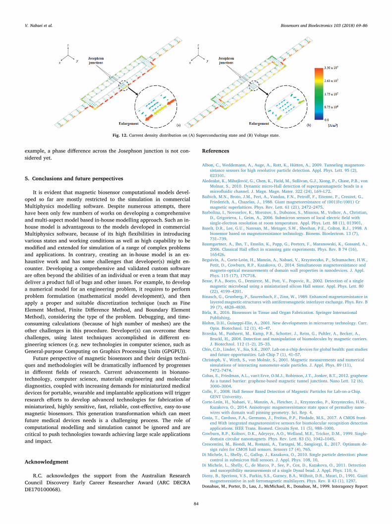
example, a phase difference across the Josephson junction is not con-sidered yet.
5. Conclusions and future perspectives
It is evident that magnetic biosensor computational models devel-oped so far are mostly restricted to the simulation in commercialMultiphysics modelling software. Despite numerous attempts, therehave been only few numbers of works on developing a comprehensiveand multi-aspect model based in-house modelling approach. Such an in-house model is advantageous to the models developed in commercialMultiphysics software, because of its high flexibilities in introducingvarious states and working conditions as well as high capability to bemodified and extended for simulation of a range of complex problemsand applications. In contrary, creating an in-house model is an ex-haustive work and has some challenges that developer(s) might en-counter. Developing a comprehensive and validated custom softwareare often beyond the abilities of an individual or even a team that maydeliver a product full of bugs and other issues. For example, to developa numerical model for an engineering problem, it requires to performproblem formulation (mathematical model development), and thenapply a proper and suitable discretization technique (such as FineElement Method, Finite Difference Method, and Boundary ElementMethod), considering the type of the problem. Debugging, and time-consuming calculations (because of high number of meshes) are theother challenges in this procedure. Developer(s) can overcome thesechallenges, using latest techniques accomplished in different en-gineering sciences (e.g. new technologies in computer science, such asGeneral-purpose Computing on Graphics Processing Units (GPGPU)).
Future perspective of magnetic biosensors and their design techni-ques and methodologies will be dramatically influenced by progressesin different fields of research. Current advancements in bionano-technology, computer science, materials engineering and moleculardiagnostics, coupled with increasing demands for miniaturized medicaldevices for portable, wearable and implantable applications will triggerresearch efforts to develop advanced technologies for fabrication ofminiaturized, highly sensitive, fast, reliable, cost-effective, easy-to-usemagnetic biosensors. This generation transformation which can meetfuture medical devices needs is a challenging process. The role ofcomputational modelling and simulation cannot be ignored and arecritical to push technologies towards achieving large scale applicationsand impact.
Acknowledgment
R.C. acknowledges the support from the Australian ResearchCouncil Discovery Early Career Researcher Award (ARC DECRADE170100068).
References
Albon, C., Weddemann, A., Auge, A., Rott, K., Hütten, A., 2009. Tunneling magnetore-sistance sensors for high resolutive particle detection. Appl. Phys. Lett. 95 (2),023101.
Aledealat, K., Mihajlović, G., Chen, K., Field, M., Sullivan, G.J., Xiong, P., Chase, P.B., vonMolnar, S., 2010. Dynamic micro-Hall detection of superparamagnetic beads in amicrofluidic channel. J. Magn. Magn. Mater. 322 (24), L69–L72.
Baibich, M.N., Broto, J.M., Fert, A., Vandau, F.N., Petroff, F., Eitenne, P., Creuzet, G.,Friederich, A., Chazelas, J., 1988. Giant magnetoresistance of (001)Fe/(001) Crmagnetic superlattices. Phys. Rev. Lett. 61 (21), 2472–2475.
Barbolina, I., Novoselov, K., Morozov, S., Dubonos, S., Missous, M., Volkov, A., Christian,D., Grigorieva, I., Geim, A., 2006. Submicron sensors of local electric field withsingle-electron resolution at room temperature. Appl. Phys. Lett. 88 (1), 013901.
Baselt, D.R., Lee, G.U., Natesan, M., Metzger, S.W., Sheehan, P.E., Colton, R.J., 1998. Abiosensor based on magnetoresistance technology. Biosens. Bioelectron. 13 (7),731–739.
Baumgartner, A., Ihn, T., Ensslin, K., Papp, G., Peeters, F., Maranowski, K., Gossard, A.,2006. Classical Hall effect in scanning gate experiments. Phys. Rev. B 74 (16),165426.
Beguivin, A., Corte-León, H., Manzin, A., Nabaei, V., Krzysteczko, P., Schumacher, H.W.,Petit, D., Cowburn, R.P., Kazakova, O., 2014. Simultaneous magnetoresistance andmagneto-optical measurements of domain wall properties in nanodevices. J. Appl.Phys. 115 (17), 17C718.
Besse, P.A., Boero, G., Demierre, M., Pott, V., Popovic, R., 2002. Detection of a singlemagnetic microbead using a miniaturized silicon Hall sensor. Appl. Phys. Lett. 80(22), 4199–4201.
Binasch, G., Grunberg, P., Saurenbach, F., Zinn, W., 1989. Enhanced magnetoresistance inlayered magnetic-structures with antiferromagnetic interlayer exchange. Phys. Rev. B39 (7), 4828–4830.
Birla, R., 2016. Biosensors in Tissue and Organ Fabrication. Springer InternationalPublishing.
Blohm, D.H., Guiseppi-Elie, A., 2001. New developments in microarray technology. Curr.Opin. Biotechnol. 12 (1), 41–47.
Brzeska, M., Panhorst, M., Kamp, P.B., Schotter, J., Reiss, G., Puhler, A., Becker, A.,Bruckl, H., 2004. Detection and manipulation of biomolecules by magnetic carriers.J. Biotechnol. 112 (1–2), 25–33.
Chin, C.D., Linder, V., Sia, S.K., 2007. Lab-on-a-chip devices for global health: past studiesand future opportunities. Lab Chip 7 (1), 41–57.
Christoph, V., Wirth, S., von Molnár, S., 2001. Magnetic measurements and numericalsimulations of interacting nanometer-scale particles. J. Appl. Phys. 89 (11),7472–7474.
Cobas, E., Friedman, A.L., van't Erve, O.M.J., Robinson, J.T., Jonker, B.T., 2012. grapheneAs a tunnel barrier: graphene-based magnetic tunnel junctions. Nano Lett. 12 (6),3000–3004.
Colle, F., 2008. Hall Sensor Based Detection of Magnetic Particles for Lab-on-a-Chip.GENT University.
Corte-León, H., Nabaei, V., Manzin, A., Fletcher, J., Krzysteczko, P., Krzysteczko, H.W.,Kazakova, O., 2014. Anisotropic magnetoresistance state space of permalloy nano-wires with domain wall pinning geometry. Sci. Rep. 4.
Costa, T., Cardoso, F.A., Germano, J., Freitas, P.P., Piedade, M.S., 2017. A CMOS front-end With integrated magnetoresistive sensors for biomolecular recognition detectionapplications. IEEE Trans. Biomed. Circuits Syst. 11 (5), 988–1000.
Cowburn, R.P., Koltsov, D.K., Adeyeye, A.O., Welland, M.E., Tricker, D.M., 1999. Single-domain circular nanomagnets. Phys. Rev. Lett. 83 (5), 1042–1045.
Crescentini, M., Biondi, M., Romani, A., Tartagni, M., Sangiorgi, E., 2017. Optimum de-sign rules for CMOS hall sensors. Sensors 17 (4), 765.
Di Michele, L., Shelly, C., Gallop, J., Kazakova, O., 2010. Single particle detection: phasecontrol in submicron Hall sensors. J. Appl. Phys. 108, 10.
Di Michele, L., Shelly, C., de Marco, P., See, P., Cox, D., Kazakova, O., 2011. Detectionand susceptibility measurements of a single Dynal bead. J. Appl. Phys. 110, 6.
Dieny, B., Speriosu, V.S., Parkin, S.S., Gurney, B.A., Wilhoit, D.R., Mauri, D., 1991. Giantmagnetoresistive in soft ferromagnetic multilayers. Phys. Rev. B 43 (1), 1297.
Donahue, M., Porter, D., Lau, J., McMichael, R., Donahue, M., 1999. Interagency Report
Fig. 12. Current density distribution on (A) Superconducting state and (B) Voltage state.
V. Nabaei et al. Biosensors and Bioelectronics 103 (2018) 69–86
84

NISTIR 6376. NIST J. Res. National Institute of Standards and Technology,Gaithersburg, vol. 114, pp. 57–67.
Donahue, M.J., 1999. OOMMF User's Guide, Version 1.0. -6376.Donolato, M., Gobbi, M., Vavassori, P., Leone, M., Cantoni, M., Metlushko, V., Ilic, B.,
Zhang, M., Wang, S.X., Bertacco, R., 2009. Nanosized corners for trapping and de-tecting magnetic nanoparticles. Nanotechnology 20 (38), 385501.
Donolato, M., Vavassori, P., Gobbi, M., Deryabina, M., Hansen, M.F., Metlushko, V., Ilic,B., Cantoni, M., Petti, D., Brivio, S., Bertacco, R., 2010. On-chip manipulation ofprotein-coated magnetic beads via domain-wall conduits. Adv. Mater. 22 (24), 2706.
Ennen, I., Kappe, D., Rempel, T., Glenske, C., Hütten, A., 2016. Giant magnetoresistance:basic concepts, microstructure, magnetic interactions and applications. Sensors 16(6), 904.
Enpuku, K., Inoue, K., Soejima, K., Yoshinaga, K., Kuma, H., Hamasaki, N., 2005.Magnetic immunoassays utilizing magnetic markers and a high-T/sub c/SQUID. IEEETrans. Appl. Supercond. 15 (2), 660–663.
Enserink, M., 2001. Biodefense hampered by inadequate tests. Science 294 (5545),1266–1267.
Folks, L., Troup, A., Boone, T., Katine, J., Nishioka, M., Grobis, M., Sullivan, G., Ikhlassi,A., Field, M., Gurney, B., 2009. Near-surface nanoscale InAs Hall cross sensitivity tolocalized magnetic and electric fields. J. Phys.: Condens. Matter 21 (25), 255802.
Gallagher, W.J., Parkin, S.S.P., Lu, Y., Bian, X.P., Marley, A., Roche, K.P., Altman, R.A.,Rishton, S.A., Jahnes, C., Shaw, T.M., Xiao, G., 1997. Microstructured magnetictunnel junctions. J. Appl. Phys. 81 (8), 3741–3746.
Gijs, M.A.M., 2004. Magnetic bead handling on-chip: new opportunities for analyticalapplications. Microfluid Nanofluid 1 (1), 22–40.
Gomez, R.D., Luu, T.V., Pak, A.O., Kirk, K.J., Chapman, J.N., 1999. Domain configura-tions of nanostructured permalloy elements. J. Appl. Phys. 85 (8), 6163–6165.
Graham, D.L., Ferreira, H.A., Freitas, P.P., 2004. Magnetoresistive-based biosensors andbiochips. Trends Biotechnol. 22 (9), 455–462.
Graham, D.L., Ferreira, H.A., Feliciano, N., Freitas, P.P., Clarke, L.A., Amaral, M.D., 2005.Magnetic field-assisted DNA hybridisation and simultaneous detection using micron-sized spin-valve sensors and magnetic nanoparticles. Sens. Actuators B Chem. 107(2), 936–944.
Guslienko, K.Y., Novosad, V., Otani, Y., Shima, H., Fukamichi, K., 2002. Magnetizationreversal due to vortex nucleation, displacement, and annihilation in submicron fer-romagnetic dot arrays. Phys. Rev. B 65, 2.
Haun, J.B., Devaraj, N.K., Hilderbrand, S.A., Lee, H., Weissleder, R., 2010. Bioorthogonalchemistry amplifies nanoparticle binding and enhances the sensitivity of cell detec-tion. Nat. Nanotechnol. 5 (9), 660–665.
Heidari, H., Bonizzoni, E., Gatti, U., Maloberti, F., 2014. A current-mode CMOS integratedmicrosystem for current spinning magnetic Hall sensors. IEEE Int. Symp. CircuitsSyst. 678–681.
Heidari, H., Bonizzoni, E., Gatti, U., Maloberti, F., 2015. A CMOS current-mode magneticHall sensor With integrated front-end. IEEE Trans. Circuits Syst. I Regul. Pap. 62 (5),1270–1278.
Heidari, H., Bonizzoni, E., Gatti, U., Maloberti, F., Dahiya, R., 2016. CMOS vertical Hallmagnetic sensors on flexible substrate. IEEE Sens. J. 16 (24), 8736–8743.
Heidari, H., Gatti, U., Bonizzoni, E., Maloberti, F., 2013. Low-Noise Low-Offset Current-Mode Hall Sensors. In: Proceedings of the IEEE Conference on Ph.D. Research inMicroelectronics and Electronics (PRIME), pp. 325–328.
Hengstmann, T.M., Grundler, D., Heyn, C., Heitmann, D., 2001. Stray-field investigationon permalloy nanodisks. J. Appl. Phys. 90 (12), 6542–6544.
Huang, C.-C., Zhou, X., Hall, D.A., 2017. Giant magnetoresistive biosensors for time-do-main magnetorelaxometry: a theoretical investigation and progress toward an im-munoassay. Sci. Rep. 7.
Issadore, D., Chung, H.J., Chung, J., Budin, G., Weissleder, R., Lee, H., 2013. μHall chipfor sensitive detection of bacteria. Adv. Healthc. Mater. 2 (9), 1224–1228.
Kazakova, O., Gallop, J., Perkins, G., Cohen, L., 2007. Scanned micro-Hall microscope fordetection of biofunctionalized magnetic beads. Appl. Phys. Lett. 90 (16).
Kazakova, O., Panchal, V., Gallop, J., See, P., Cox, D.C., Spasova, M., Cohen, L.F., 2010.Ultrasmall particle detection using a submicron Hall sensor. J. Appl. Phys. 107, 9.
Khan, M., Henk, J., Bruno, P., 2008. Anisotropic magnetoresistance in Fe/MgO/Fe tunneljunctions. J. Phys.: Condens. Matter 20 (15), 155208.
Kim, K.W., Reddy, V., Torati, S.R., Hu, X.H., Sandhu, A., Kim, C.G., 2015. On-chipmagnetometer for characterization of superparamagnetic nanoparticles. Lab Chip 15(3), 696–703.
Kirk, K.J., Chapman, J.N., Wilkinson, C.D.W., 1997. Switching fields and magnetostaticinteractions of thin film magnetic nanoelements. Appl. Phys. Lett. 71 (4), 539–541.
Koh, I., Josephson, L., 2009. Magnetic nanoparticle sensors. Sensors 9 (10), 8130–8145.Kotitz, R., Matz, H., Trahms, L., Koch, H., Weitschies, W., Rheinlander, T., Semmler, W.,
Bunte, T., 1997. SQUID based remanence measurements for immunoassays. IEEETrans. Appl. Supercond. 7 (2), 3678–3681.
Krause, H.J., Kreutzbruck, M.V., 2002. Recent developments in SQUID NDE. Phys. C:Supercond. 368 (1), 70–79.
Krishna, V.D., Wu, K., Perez, A.M., Wang, J.-P., 2016. Giant Magnetoresistance-basedbiosensor for detection of influenza A virus. Front. Microbiol. 7.
Kumagai, Y., Imai, Y., Abe, M., Sakamoto, S., Handa, H., Sandhu, A., 2008. Sensitivitydependence of Hall biosensor arrays with the position of superparamagnetic beads ontheir active regions. J. Appl. Phys. 103 (7), 07A309.
Landry, G., Miller, M.M., Bennett, B.R., Johnson, M., Smolyaninova, V., 2004.Characterization of single magnetic particles with InAs quantum-well Hall devices.Appl. Phys. Lett. 85 (20), 4693–4695.
Lee, W., Joo, S., Kim, S.U., Rhie, K., Hong, J., Shin, K.-H., Kim, K.H., 2009. Magnetic beadcounter using a micro-Hall sensor for biological applications. Appl. Phys. Lett. 94(15), 153903.
Lenz, J., Edelstein, S., 2006. Magnetic sensors and their applications. IEEE Sens. J. 6 (3),
631–649.Lenz, J.E., 1990. A review of magnetic sensors. Proc. IEEE 78 (6), 973–989.Li, F., Kosel, J., 2012. A magnetic method to concentrate and trap biological targets. IEEE
Trans. Magn. 48 (11), 2854–2856.Li, F., Kosel, J., 2013. A magnetic biosensor system for detection of E. coli. IEEE Trans.
Magn. 49 (7), 3492–3495.Li, F., Kosel, J., 2014. An efficient biosensor made of an electromagnetic trap and a
magneto-resistive sensor. Biosens. Bioelectron. 59, 145–150.Li, G., Joshi, V., White, R.L., Wang, S.X., Kemp, J.T., Webb, C., Davis, R.W., Sun, S.,
2003a. Detection of single micron-sized magnetic bead and magnetic nanoparticlesusing spin valve sensors for biological applications. J. Appl. Phys. 93 (10),7557–7559.
Li, G.X., Joshi, V., White, R.L., Wang, S.X., Kemp, J.T., Webb, C., Davis, R.W., Sun, S.H.,2003b. Detection of single micron-sized magnetic bead and magnetic nanoparticlesusing spin valve sensors for biological applications. J. Appl. Phys. 93 (10),7557–7559.
Li, G.X., Sun, S.H., Wilson, R.J., White, R.L., Pourmand, N., Wang, S.X., 2006. Spin valvesensors for ultrasensitive detection of superparamagnetic nanoparticles for biologicalapplications. Sens. Actuators a Phys. 126 (1), 98–106.
Li, Y., Srinivasan, B., Jing, Y., Yao, X., Hugger, M.A., Wang, J.-P., Xing, C., 2010.Nanomagnetic competition assay for low-abundance protein biomarker quantifica-tion in unprocessed human sera. J. Am. Chem. Soc. 132 (12), 4388–4392.
Li, Y., Wang, Y., Klein, T., Wang, J.-P., 2014. External-field-free magnetic biosensor. Appl.Phys. Lett. 104 (12), 122401.
Li, Z., De Groot, C., Moodera, J.H., 2000. Gallium oxide as an insulating barrier for spin-dependent tunneling junctions. Appl. Phys. Lett. 77 (22), 3630–3632.
Liu, Y., Jin, W., Yang, Y., Wang, Z., 2006. Micromagnetic simulation for detection of asingle magnetic microbead or nanobead by spin-valve sensors. J. Appl. Phys. 99 (8)(08G102).
Llandro, J., Hayward, T., Morecroft, D., Bland, J., Castaño, F., Colin, I., Ross, C., 2007.Quantitative digital detection of magnetic beads using pseudo-spin-valve rings formultiplexed bioassays. Appl. Phys. Lett. 91 (20), 203904.
Llandro, J., Palfreyman, J.J., Ionescu, A., Barnes, C.H.W., 2010. Magnetic biosensortechnologies for medical applications: a review. Med. Biol. Eng. Comput. 48 (10),977–998.
Manandhar, P., Chen, K.S., Aledealat, K., Mihajlovic, G., Yun, C.S., Field, M., Sullivan,G.J., Strouse, G.F., Chase, P.B., von Molnar, S., Xiong, P., 2009. The detection ofspecific biomolecular interactions with micro-Hall magnetic sensors. Nanotechnology20 (35).
Manzin, A., Nabaei, V., 2014. Modelling of micro-Hall sensors for magnetization imaging.J. Appl. Phys. 115 (17), 17E506.
Manzin, A., Nabaei, V., Kazakova, O., 2012. Modelling and optimization of submicronHall sensors for the detection of superparamagnetic beads. J. Appl. Phys. 111 (7)(07E513).
Manzin, A., Nabaei, V., Corte-León, H., Kazakova, O., Krzysteczko, P., Schumacher, H.W.,2014. Modeling of anisotropic magnetoresistance properties of permalloy nanos-tructures. IEEE Trans. Magn. 50 (4), 1–4.
Mcguire, T.R., Potter, R.I., 1975. Anisotropic magnetoresistance in ferromagnetic 3d al-loys. IEEE Trans. Magn. 11 (4), 1018–1038.
Mihajlovic, G., Xiong, P., von Molnar, S., Ohtani, K., Ohno, H., Field, M., Sullivan, G.J.,2005. Detection of single magnetic bead for biological applications using an InAsquantum-well micro-Hall sensor. Appl. Phys. Lett. 87 (11).
Mihajlovic, G., Aledealat, K., Xiong, P., Von Molnar, S., Field, M., Sullivan, G.J., 2007.Magnetic characterization of a single superparamagnetic bead by phase-sensitivemicro-Hall magnetometry. Appl. Phys. Lett. 91 (17).
Miller, M.M., Prinz, G.A., Cheng, S.F., Bounnak, S., 2002. Detection of a micron-sizedmagnetic sphere using a ring-shaped anisotropic magnetoresistance-based sensor: amodel for a magnetoresistance-based biosensor. Appl. Phys. Lett. 81 (12),2211–2213.
Miyazaki, T., Tezuka, N., 1995. Giant magnetic tunneling effect in Fe/Al2O3/Fe junction.J. Magn. Magn. Mater. 139 (3), L231–L234.
Moodera, J.S., Kinder, L.R., Wong, T.M., Meservey, R., 1995. Large magnetoresistance atroom temperature in ferromagnetic thin film tunnel junctions. Phys. Rev. Lett. 74(16), 3273.
Moura-Melo, W.A., Pereira, A.R., Silva, R.L., Oliveira, N.M., 2008. How hole defectsmodify vortex dynamics in ferromagnetic nanodisks. J. Appl. Phys. 103, 12.
Munoz-Rojas, F., Fernandez-Rossier, J., Palacios, J.J., 2009. Giant magnetoresistance inultrasmall graphene based devices. Phys. Rev. Lett. 102, 13.
Nabaei, V., 2014. Modelling of Nanostructured Devices for Magnetic SensingApplications. Polytechnic University of Turin.
Nabaei, V., Rajkumar, R., Manzin, A., Kazakova, O., Tzalenchuk, A., 2013. Optimizationof Hall bar response to localized magnetic and electric fields. J. Appl. Phys. 113 (6),064504.
Nazari Nejad, S., 2015. Miniature Magnetic Sensors.O'handley, R.C., 2000. Modern Magnetic Materials: Principles and Applications. Wiley.Pankhurst, Q.A., Connolly, J., Jones, S.K., Dobson, J., 2003. Applications of magnetic
nanoparticles in biomedicine. J. Phys. D. Appl. Phys. 36 (13), R167–R181.Parkin, S.S.P., Kaiser, C., Panchula, A., Rice, P.M., Hughes, B., Samant, M., Yang, S.-H.,
2004a. Giant tunnelling magnetoresistance at room temperature with MgO (100)tunnel barriers. Nat. Mater. 3 (12), 862–867.
Parkin, S.S.P., Kaiser, C., Panchula, A., Rice, P.M., Hughes, B., Samant, M., Yang, S.H.,2004b. Giant tunnelling magnetoresistance at room temperature with MgO (100)tunnel barriers. Nat. Mater. 3 (12), 862–867.
Pratt, W.P., Lee, S.F., Slaughter, J.M., Loloee, R., Schroeder, P.A., Bass, J., 1991.Perpendicular giant magnetoresistances of Ag/Co multilayers. Phys. Rev. Lett. 66(23), 3060–3063.
V. Nabaei et al. Biosensors and Bioelectronics 103 (2018) 69–86
85

Prejbeanu, I.L., Natali, M., Buda, L.D., Ebels, U., Lebib, A., Chen, Y., Ounadjela, K., 2002.In-plane reversal mechanisms in circular Co dots. J. Appl. Phys. 91 (10), 7343–7345.
Prinz, G.A., 1998. Magnetoelectronics. Science 282 (5394), 1660–1663.Pulwey, R., Rahm, M., Biberger, J., Weiss, D., 2001. Switching behavior of vortex
structures in nanodisks. Ieee Trans. Magn. 37 (4), 2076–2078.Qiu, J., Liu, J.-.G., Zhang, Q., Lin, J., 2014. Simulation and optimization of conductor
structural parameters of free-space hall-effect current sensor. In: Proceedings of the2014 IEEE International Workshop on Applied Measurements for Power SystemsProceedings (AMPS), pp. 1–6.
Raabe, J., Pulwey, R., Sattler, R., Schweinbock, T., Zweck, J., Weiss, D., 2000.Magnetization pattern of ferromagnetic nanodisks. J. Appl. Phys. 88 (7), 4437–4439.
Rahm, M., Biberger, J., Umansky, V., Weiss, D., 2003a. Vortex pinning at individualdefects in magnetic nanodisks. J. Appl. Phys. 93 (10), 7429–7431.
Rahm, M., Schneider, M., Biberger, J., Pulwey, R., Zweck, J., Weiss, D., Umansky, V.,2003b. Vortex nucleation in submicrometer ferromagnetic disks. Appl. Phys. Lett. 82(23), 4110–4112.
Rahm, M., Hollinger, R., Umansky, V., Weiss, D., 2004a. Influence of point defects onmagnetic vortex structures. J. Appl. Phys. 95 (11), 6708–6710.
Rahm, M., Stahl, J., Wegscheider, W., Weiss, D., 2004b. Multistable switching due tomagnetic vortices pinned at artificial pinning sites. Appl. Phys. Lett. 85 (9),1553–1555.
Reiss, G., Brueckl, H., Huetten, A., Schotter, J., Brzeska, M., Panhorst, M., Sudfeld, D.,Becker, A., Kamp, P.B., Puehler, A., 2005. Magnetoresistive sensors and magneticnanoparticles for biotechnology. J. Mater. Res. 20 (12), 3294–3302.
Rizzi, G., Lee, J.-R., Guldberg, P., Dufva, M., Wang, S.X., Hansen, M.F., 2017.Denaturation strategies for detection of double stranded PCR products on GMRmagnetic biosensor array. Biosens. Bioelectron. 93, 155–160.
Ruan, G., Vieira, G., Henighan, T., Chen, A.R., Thakur, D., Sooryakumar, R., Winter, J.O.,2010. Simultaneous magnetic manipulation and fluorescent tracking of multiple in-dividual hybrid nanostructures. Nano Lett. 10 (6), 2220–2224.
Sagadevan, S., Periasamy, M., 2014. Recent trends in nanobiosensors and their applica-tions-a review. Rev. Adv. Mater. Sci. 36, 62–69.
Sandhu, A., Sanbonsugi, H., Shibasaki, I., Abe, M., Handa, H., 2004. High sensitivity InSbultra-thin film micro-Hall sensors for bioscreening applications. Jpn. J. Appl. Phys. 43(7A), L868.
Sandhu, A., Kumagai, Y., Lapicki, A., Sakamoto, S., Abe, M., Handa, H., 2007. High ef-ficiency Hall effect micro-biosensor platform for detection of magnetically labeledbiomolecules. Biosens. Bioelectron. 22 (9–10), 2115–2120.
Schneider, M., Hoffmann, H., Zweck, J., 2000. Lorentz microscopy of circular ferro-magnetic permalloy nanodisks. Appl. Phys. Lett. 77 (18), 2909–2911.
Schneider, M., Hoffmann, H., Otto, S., Haug, T., Zweck, J., 2002. Stability of magneticvortices in flat submicron permalloy cylinders. J. Appl. Phys. 92 (3), 1466–1472.
Schneider, M., Liszkowski, J., Rahm, M., Wegscheider, W., Weiss, D., Hoffmann, H.,Zweck, J., 2003. Magnetization configurations and hysteresis loops of small per-malloy ellipses. J. Phys. D. Appl. Phys. 36 (18), 2239–2243.
Schotter, J., Kamp, P.B., Becker, A., Puhler, A., Brinkmann, D., Schepper, W., Bruckl, H.,Reiss, G., 2002. A biochip based on magnetoresistive sensors. IEEE Trans. Magn. 38(5), 3365–3367.
Schotter, J., Kamp, P.B., Becker, A., Puhler, A., Reiss, G., Bruckl, H., 2004. Comparison ofa prototype magnetoresistive biosensor to standard fluorescent DNA detection.Biosens. Bioelectron. 19 (10), 1149–1156.
Schuh, D., Biberger, J., Bauer, A., Breuer, W., Weiss, D., 2001. Hall-magnetometry onferromagnetic dots and dot arrays. IEEE Trans. Magn. 37 (4), 2091–2093.
Shen, W.F., Liu, X.Y., Mazumdar, D., Xiao, G., 2005. In situ detection of single micron-sized magnetic beads using magnetic tunnel junction sensors. Appl. Phys. Lett.86 (25).
Tamanaha, C., Mulvaney, S., Rife, J., Whitman, L., 2008. Magnetic labeling, detection,and system integration. Biosens. Bioelectron. 24 (1), 1–13.
Terauchi, N., Noguchi, S., Igarashi, H., Hatsukade, Y., Tanaka, S., 2012. Characteristicanalysis of directly coupled HTS dc-SQUID magnetometer with superconducting filmmagnetic-shield considering Josephson-junction resistance. IEEE Trans. Magn. 48 (2),571–574.
Terauchi, N., Noguchi, S., Igarashi, H., 2014. Numerical simulation of SQUID magnet-ometer considering equivalent electrical circuit of Josephson junction. Phys. Procedia58, 200–203.
Thomson, W., 1856. On the electro-dynamic qualities of metals:–effects of magnetizationon the electric conductivity of nickel and of iron. Proc. R. Soc. Lond. 8, 546–550.
Tsukamoto, A., Saitoh, K., Suzuki, D., Sugita, N., Seki, Y., Kandori, A., Tsukada, K.,Sugiura, Y., Hamaoka, S., Kuma, H., 2005. Development of multisample biologicalimmunoassay system using HTSSQUID and magnetic nanoparticles. IEEE Trans. Appl.Supercond. 15 (2), 656–659.
Tumanski, S., 2001. Thin Film Magnetoresistive Sensors. CRC Press.Tumanski, S., 2016. Handbook of Magnetic Measurements. CRC Press.Vavassori, P., Metlushko, V., Ilic, B., Gobbi, M., Donolato, M., Cantoni, M., Bertacco, R.,
2008. Domain wall displacement in Py square ring for single nanometric magneticbead detection. Appl. Phys. Lett. 93 (20), 203502.
Vieira, G., Henighan, T., Chen, A., Hauser, A.J., Yang, F.Y., Chalmers, J.J., Sooryakumar,R., 2009. Magnetic wire traps and programmable manipulation of biological cells.Phys. Rev. Lett. 103, 12.
Vieira, G., Chen, A., Henighan, T., Lucy, J., Yang, F.Y., Sooryakumar, R., 2012. Transportof magnetic microparticles via tunable stationary magnetic traps in patterned wires.Phys. Rev. B 85, 17.
Wang, S.X., Bae, S.Y., Li, G.X., Sun, S.H., White, R.L., Kemp, J.T., Webb, C.D., 2005.Towards a magnetic microarray for sensitive diagnostics. J. Magn. Magn. Mater. 293(1), 731–736.
Wang, T., Zhou, Y., Lei, C., Luo, J., Xie, S., Pu, H., 2017. Magnetic impedance biosensor: areview. Biosens. Bioelectron. 90, 418–435.
Williams, E.M., 2001. Design and Analysis of Magnetoresistive Recording Heads. J Wiley.Wirix-Speetjens, R., Fyen, W., De Boeck, J., Borghs, G., 2006. Single magnetic particle
detection: experimental verification of simulated behavior. J. Appl. Phys. 99 (10),103903.
Xu, J., Li, Q., Zong, W., Zhang, Y., Li, S., 2016. Ultra-wide detectable concentration rangeof GMR biosensors using Fe3O4 microspheres. J. Magn. Magn. Mater. 417, 25–29.
Yuasa, S., Nagahama, T., Fukushima, A., Suzuki, Y., Ando, K., 2004. Giant room-tem-perature magnetoresistance in single-crystal Fe/MgO/Fe magnetic tunnel junctions.Nat. Mater. 3 (12), 868–871.
V. Nabaei et al. Biosensors and Bioelectronics 103 (2018) 69–86
86