bga 8m x 36 533 mhz 300 mhz industrial temp 288mb cio low
TRANSCRIPT

GS4288C36GL
8M x 36288Mb CIO Low Latency DRAM (LLDRAM) II
533 MHz–300 MHz 2.5 V VEXT 1.8 V VDD
1.5 V or 1.8 V VDDQ
144-Ball BGACommercial TempIndustrial Temp
Rev: 1.04 4/2018 1/60 © 2011, GSI TechnologySpecifications cited are subject to change without notice. For latest documentation see http://www.gsitechnology.com.
Features• Pin- and function-compatible with Micron RLDRAM® II• 533 MHz DDR operation (1.067Gb/s/pin data rate)• 38.4 Gb/s peak bandwidth (x36 at 533 MHz clock frequency)• 8M x 36 organization available• 8 internal banks for concurrent operation and maximum
bandwidth• Reduced cycle time (15 ns at 533 MHz)• Address Multiplexing (Nonmultiplexed address option
available) • SRAM-type interface• Programmable Read Latency (RL), row cycle time, and burst
sequence length• Balanced Read and Write Latencies in order to optimize data
bus utilization• Data mask for Write commands• Differential input clocks (CK, CK)• Differential input data clocks (DKx, DKx)• On-chip DLL generates CK edge-aligned data and output
data clock signals• Data valid signal (QVLD)• 32 ms refresh (8K refresh for each bank; 64K refresh
command must be issued in total each 32 ms)• 144-ball BGA package• HSTL I/O (1.5 V or 1.8 V nominal)• 25–60 matched impedance outputs• 2.5 V VEXT, 1.8 V VDD, 1.5 V or 1.8 V VDDQ I/O
• On-die termination (ODT) RTT
• Commerical and Industrial TemperatureCommercial (+0° TC +95°C)
Industrial (–40° TC +95°C)
IntroductionThe GSI Technology 288Mb Low Latency DRAM (LLDRAM) II is a high speed memory device designed for high address rate data processing typically found in networking and telecommunications applications. The 8-bank architecture and low tRC allows access rates formerly only found in SRAMs.
The Double Data Rate (DDR) I/O interface provides high bandwidth data transfers, clocking out two beats of data per clock cycle at the I/O balls. Source-synchronous clocking can be implemented on the host device with the provided free-running data output clock.
Commands, addresses, and control signals are single data rate signals clocked in by the True differential input clock transition, while input data is clocked in on both crossings of the input data clock(s).
Read and Write data transfers always in short bursts. The burst length is programmable to 2, 4 or 8 by setting the Mode Register.
The device is supplied with 2.5 V VEXT and 1.8 V VDD for the
core, and 1.5 V or 1.8 V for the HSTL output drivers.
Internally generated row addresses facilitate bank-scheduled refresh.
The device is delivered in an efficent BGA 144-ball package.

GS4288C36GL
Specifications cited are subject to change without notice. For latest documentation see http://www.gsitechnology.com.
Rev: 1.04 4/2018 2/60 © 2011, GSI Technology
8M x 36 Ball Assignments—144-Ball BGA—Top View
1 2 3 4 5 6 7 8 9 10 11 12
A VREF VSS VEXT VSS VSS VEXT TMS TCK
B VDD DQ8 DQ9 VSS VSS DQ1 DQ0 VDD
C VTT DQ10 DQ11 VDDQ VDDQ DQ3 DQ2 VTT
D A221 DQ12 DQ13 VSS VSS QK0 QK0 VSS
E A211 DQ14 DQ15 VDDQ VDDQ DQ5 DQ4 A202
F A5 DQ16 DQ17 VSS VSS DQ7 DQ6 QVLD
G A8 A6 A7 VDD VDD A2 A1 A0
H B2 A9 VSS VSS VSS VSS A4 A3
J DK0 DK0 VDD VDD VDD VDD B0 CK
K DK1 DK1 VDD VDD VDD VDD B1 CK
L REF CS VSS VSS VSS VSS A14 A13
M WE A16 A17 VDD VDD A12 A11 A10
N A18 DQ24 DQ25 VSS VSS DQ35 DQ34 A192
P A15 DQ22 DQ23 VDDQ VDDQ DQ33 DQ32 DM
R VSS QK1 QK1 VSS VSS DQ31 DQ30 VSS
T VTT DQ20 DQ21 VDDQ VDDQ DQ29 DQ28 VTT
U VDD DQ18 DQ19 VSS VSS DQ27 DQ26 VDD
V VREF ZQ VEXT VSS VSS VEXT TDO TDI
Notes:1. Reserved for future use. This pin may be connected to GND.2. Reserved for future use. This pin may have parasitic characteristics of an address pin. It may be connected to GND.

GS4288C36GL
Specifications cited are subject to change without notice. For latest documentation see http://www.gsitechnology.com.
Rev: 1.04 4/2018 3/60 © 2011, GSI Technology
Ball Descriptions
Symbol Type Description
A0–A20 InputAddress Inputs—A0–A20 define the row and column addresses for Read and Write Operations. During a Mode Register Set (MRS), the address inputs define the register settings. They are sampled at the rising edge of CK.
BA0–B2 Input Bank Address inputs—Select to which internal bank a command is being applied.
CK, CK InputInput Clock—CK and CK are differential input clocks. Addresses and commands are latched on the rising edge of CK. CK is ideally 180º out of phase with CK.
CS InputChip Select—CS enables the command decoder when Low and disables it when High. When the command decoder is disabled, new commands are ignored, but internal operations continue.
DQ0–DQ35 InputData Input—The DQ signals form the 36-bit data bus. During Read commands, the data is referenced to both edges of QKx. During Write commands, the data is sampled at both edges of DK.
DK, DK Input
Input Data Clock—DK and DK are the differential input data clocks. All input data is referenced to both edges of DK. DK is ideally 180º out of phase with DK. DQ0– DQ17 are referenced to DK0 and DK0 and DQ18–DQ35 are referenced to DK1 and DK1. All DKx and DKx pins must always be supplied to the device.
DM InputInput Data Mask—The DM signal is the input mask signal for Write data. Input data is masked when DM is sampled High. DM is sampled on both edges of DK1. Tie signal to ground if not used.
TCK Input IEEE 1149.1 clock input—This ball must be tied to VSS if the JTAG function is not used.
TMS, TDI Input IEEE 1149.1 test inputs—These balls may be left as no connects if the JTAG function is not used.
WE, REF InputCommand Inputs—Sampled at the positive edge of CK, WE and REF define (together with CS) the command to be executed.
VREF Input Input Reference Voltage—Nominally VDDQ/2. Provides a reference voltage for the input buffers.
ZQ Reference
External Impedance (25–60)—This signal is used to tune the device outputs to the system data bus impedance. DQ output impedance is set to 0.2 * RQ, where RQ is a resistor from this signal to ground. Connecting ZQ to GND invokes the Minimum Impedance mode. Connecting ZQ to VDD invokes the
Maximum Impedance mode. Refer to the Mode Register Definition diagrams (Mode Register Bit 8 (M8)) to activate or deactivate this function.
QKx, QKx Output
Output Data Clocks—QKx and QKx are opposite polarity, output data clocks. They are free running,and during Reads, are edge-aligned with data output from the LLDRAM II. QKx is ideally 180º out of phase with QKx. QK0 and QK0 are aligned with DQ0–DQ17, and QK1 and QK1 are aligned with DQ18–DQ35.

GS4288C36GL
Specifications cited are subject to change without notice. For latest documentation see http://www.gsitechnology.com.
Rev: 1.04 4/2018 4/60 © 2011, GSI Technology
QVLD Output Data Valid—The QVLD pin indicates valid output data. QVLD is edge-aligned with QKx and QKx.
TDO OutputIEEE 1149.1 Test Output—JTAG output. This ball may be left as no connect if the JTAG function is not used.
VDD SupplyPower Supply—Nominally, 1.8 V. See the DC Electrical Characteristics and Operating Conditions section for range.
VDDQ SupplyDQ Power Supply—Nominally, 1.5 V or 1.8 V. Isolated on the device for improved noise immunity. See the DC Electrical Characteristics and Operating Conditions section for range.
VEXT SupplyPower Supply—Nominally, 2.5 V. See the DC Electrical Characteristics and Operating Conditions section for range.
VSS Supply Ground
VTT —Power Supply—Isolated termination supply. Nominally, VDDQ/2. See the DC Electrical Characteristics
and Operating Conditions section for range.
A21, A22 — Reserved for Future Use—This signal is not connected and may be connected to ground.
DNU — Do Not Use—These balls may be connected to ground.
NF — No Function—These balls can be connected to ground.
Ball Descriptions (Continued)
Symbol Type Description
GS4288C36GL
Specifications cited are subject to change without notice. For latest documentation see http://www.gsitechnology.com.
Rev: 1.04 4/2018 5/60 © 2011, GSI Technology
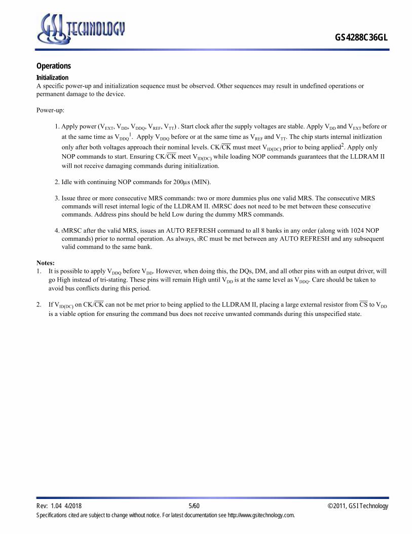
OperationsInitializationA specific power-up and initialization sequence must be observed. Other sequences may result in undefined operations or permanent damage to the device.
Power-up:
1. Apply power (VEXT, VDD, VDDQ, VREF, VTT) . Start clock after the supply voltages are stable. Apply VDD and VEXT before or
at the same time as VDDQ1. Apply VDDQ before or at the same time as VREF and VTT. The chip starts internal initlization
only after both voltages approach their nominal levels. CK/CK must meet VID(DC) prior to being applied2. Apply only
NOP commands to start. Ensuring CK/CK meet VID(DC) while loading NOP commands guarantees that the LLDRAM II
will not receive damaging commands during initialization.
2. Idle with continuing NOP commands for 200s (MIN).
3. Issue three or more consecutive MRS commands: two or more dummies plus one valid MRS. The consecutive MRS commands will reset internal logic of the LLDRAM II. tMRSC does not need to be met between these consecutive commands. Address pins should be held Low during the dummy MRS commands.
4. tMRSC after the valid MRS, issues an AUTO REFRESH command to all 8 banks in any order (along with 1024 NOP commands) prior to normal operation. As always, tRC must be met between any AUTO REFRESH and any subsequent valid command to the same bank.
Notes: 1. It is possible to apply VDDQ before VDD. However, when doing this, the DQs, DM, and all other pins with an output driver, will
go High instead of tri-stating. These pins will remain High until VDD is at the same level as VDDQ. Care should be taken to avoid bus conflicts during this period.
2. If VID(DC) on CK/CK can not be met prior to being applied to the LLDRAM II, placing a large external resistor from CS to VDD
is a viable option for ensuring the command bus does not receive unwanted commands during this unspecified state.

GS4288C36GL
Specifications cited are subject to change without notice. For latest documentation see http://www.gsitechnology.com.
Rev: 1.04 4/2018 6/60 © 2011, GSI Technology
Power–Up Initialization Sequence
200us Min Mode Initialization tMRSC Refresh 1024 Cycles NOP Cycles Min
NOP NOP MRS MRS MRS NOP AREF AREF NOP AC
CODE(1,2) CODE(1,2) CODE(2) ADDR
Bank 0 Bank 7 Valid
tDKLtDK
tDKL
tDKHtDKHtDK
tCKL
tCK
tCKLtCKHtCKH
tCK
VEXT
VDD
VDDQ
VREF
VTT
CK
CK
DK
DK
Command
ADDR
BA
DM
DQ
All Banks(5)
Notes:1. Recommend all address pins held Low during dummy MRS commands.2. A10–A17 must be Low.3. DLL must be reset if tCK or VDD are changed.4. CK and CK must be separated at all times to prevent bogus commands from being issued.5. The sequence of the eight AUTO REFRESH commands (with respect to the 1024 NOP commands) does not matter. As is required for any operation,
tRC must be met between an AUTO REFRESH command and a subsequent VALID command to the same bank.
GS4288C36GL
Specifications cited are subject to change without notice. For latest documentation see http://www.gsitechnology.com.
Rev: 1.04 4/2018 7/60 © 2011, GSI Technology
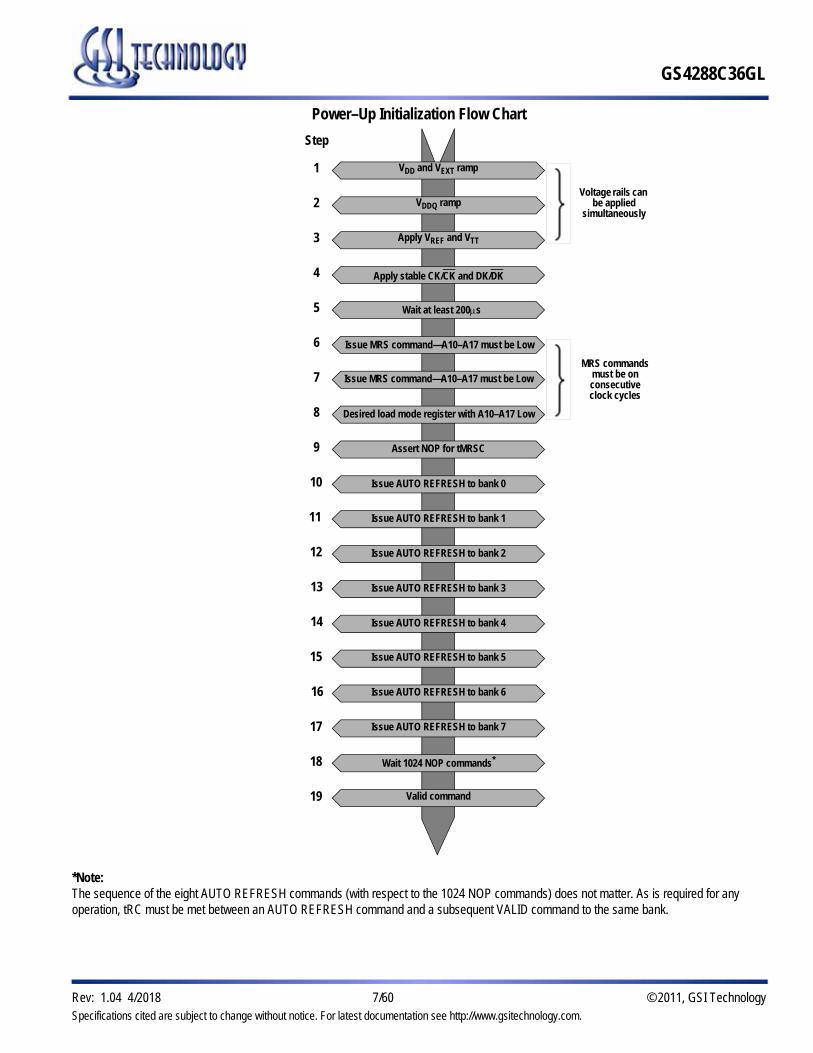
Power–Up Initialization Flow Chart
VDD and VEXT ramp
VDDQ ramp
Apply VREF and VTT
Apply stable CK/CK and DK/DK
Wait at least 200s
Issue MRS command—A10–A17 must be Low
Issue MRS command—A10–A17 must be Low
Desired load mode register with A10–A17 Low
Assert NOP for tMRSC
Issue AUTO REFRESH to bank 0
Issue AUTO REFRESH to bank 1
Issue AUTO REFRESH to bank 2
Issue AUTO REFRESH to bank 3
Issue AUTO REFRESH to bank 4
Issue AUTO REFRESH to bank 5
Issue AUTO REFRESH to bank 6
Issue AUTO REFRESH to bank 7
Wait 1024 NOP commands*
Valid command
Step
1
2
3
4
5
6
7
8
9
10
11
12
13
14
15
16
17
18
19
Voltage rails can be applied
simultaneously
MRS commands must be on consecutive clock cycles
*Note:The sequence of the eight AUTO REFRESH commands (with respect to the 1024 NOP commands) does not matter. As is required for any operation, tRC must be met between an AUTO REFRESH command and a subsequent VALID command to the same bank.

GS4288C36GL
Specifications cited are subject to change without notice. For latest documentation see http://www.gsitechnology.com.
Rev: 1.04 4/2018 8/60 © 2011, GSI Technology
DLL ResetMode Register Bit 7 (M7) selects DLL Reset as is shown in the Mode Register Definition tables. The default setting for M7 is Low, whereby the DLL is disabled. Once M7 is set High, 1024 cycles (5s at 200 MHz) are needed before a Read command can be issued. The delay allows the internal clock to be synchronized with the external clock. Failing to wait for synchronization to occur may result in a violation of the tCKQK parameter. A reset of the DLL is necessary if tCK or VDD is changed after the DLL has already been enabled. To reset the DLL, set M7 is Low. After waiting tMRSC, an MRS command should be issued to set M7 High. 1024 clock cycles must pass before loading the next Read command.
Driver Impedance MappingThe LLDRAM II is equipped with programmable impedance output buffers. Setting Mode Register Bit 8 (M8) High during the MRS command activates the feature. Programmable impedance output buffers allow the user to match the driver impedance to the PCB trace impedance. To adjust the impedance, an external resistor (RQ) is connected between the ZQ ball and VSS. The value of the resistor must be five times the desired impedance (e.g., a 300 resistor produces an output impedance of 60). RQ values of 125–300 are supported, allowing an output impedance range of 25–60 (±15%).
The drive impedance of uncompensated output transistors can change over time due to changes in supply voltage and die temperature. When drive impedance control is enabled in the MRS, the value of RQ is periodically sampled and any needed impedance update is made automatically. Updates do not affect normal device operation or signal timing.
When Bit M8 is set Low during the MRS command, the output compensation circuits are still active but reference an internal resistance reference. The internal reference is imprecise and subject to temperature and voltage variations so output buffers are set to a nominal output impedance of 50, but are subject to a ±30 percent variance over the Commercial temperature range of the device.
GS4288C36GL
Specifications cited are subject to change without notice. For latest documentation see http://www.gsitechnology.com.
Rev: 1.04 4/2018 9/60 © 2011, GSI Technology
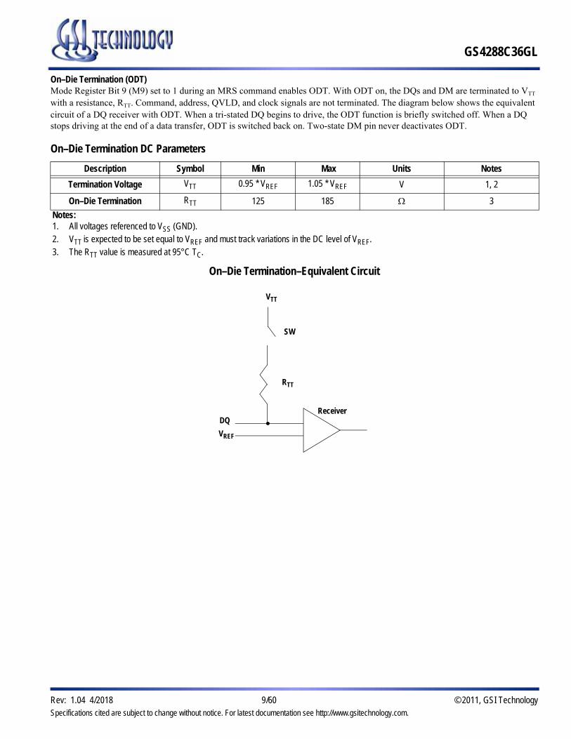
On–Die Termination (ODT)Mode Register Bit 9 (M9) set to 1 during an MRS command enables ODT. With ODT on, the DQs and DM are terminated to VTT
with a resistance, RTT. Command, address, QVLD, and clock signals are not terminated. The diagram below shows the equivalent circuit of a DQ receiver with ODT. When a tri-stated DQ begins to drive, the ODT function is briefly switched off. When a DQ stops driving at the end of a data transfer, ODT is switched back on. Two-state DM pin never deactivates ODT.
On–Die Termination DC Parameters
Description Symbol Min Max Units Notes
Termination Voltage VTT 0.95 * VREF 1.05 * VREF V 1, 2
On–Die Termination RTT 125 185 3
Notes:1. All voltages referenced to VSS (GND).2. VTT is expected to be set equal to VREF and must track variations in the DC level of VREF.3. The RTT value is measured at 95°C TC.
VTT
SW
RTT
ReceiverDQ
VREF
On–Die Termination–Equivalent Circuit
GS4288C36GL
Specifications cited are subject to change without notice. For latest documentation see http://www.gsitechnology.com.
Rev: 1.04 4/2018 10/60 © 2011, GSI Technology
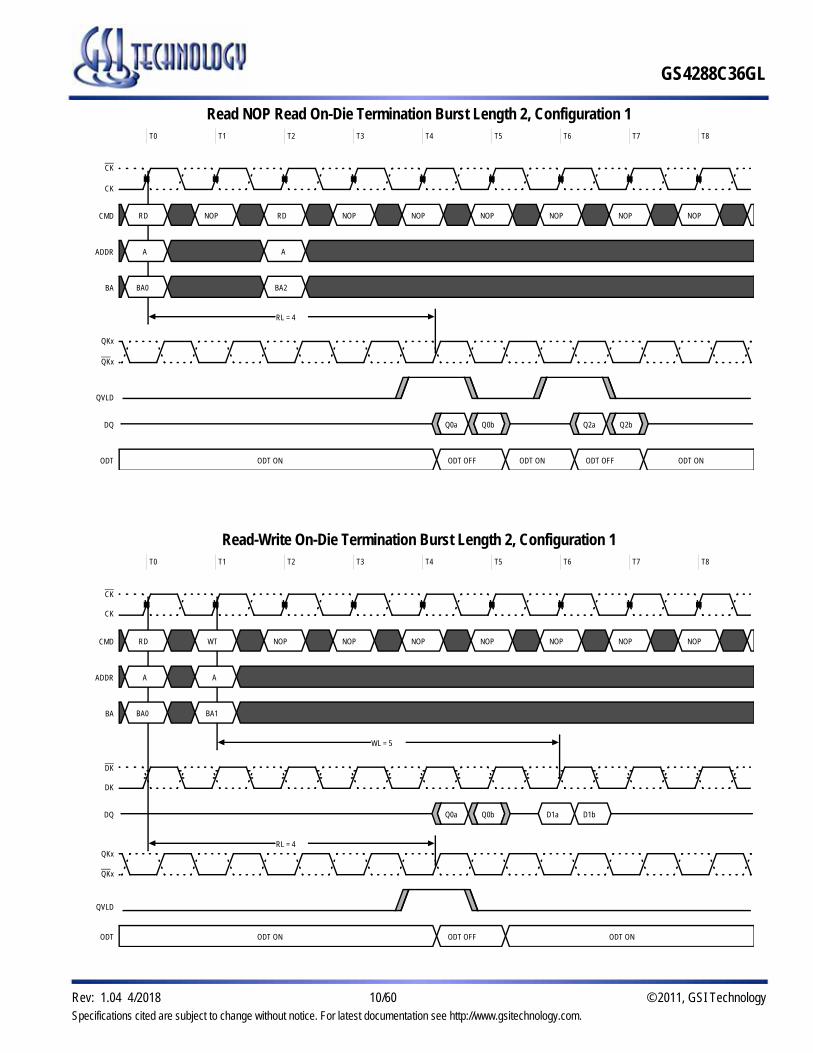
Read NOP Read On-Die Termination Burst Length 2, Configuration 1T0 T1 T2 T3 T4 T5 T6 T7 T8
RD NOP RD NOP NOP NOP NOP NOP NOP
A A
BA0 BA2
Q0a Q0b Q2a Q2b
ODT ON ODT OFF ODT ON ODT OFF ODT ON
RL = 4
CK
CK
CMD
ADDR
BA
QKx
QKx
QVLD
DQ
ODT
Read-Write On-Die Termination Burst Length 2, Configuration 1T0 T1 T2 T3 T4 T5 T6 T7 T8
RD WT NOP NOP NOP NOP NOP NOP NOP
A A
BA0 BA1
Q0a Q0b D1a D1b
ODT ON ODT OFF ODT ON
RL = 4
WL = 5
CK
CK
CMD
ADDR
BA
DK
DK
DQ
QKx
QKx
QVLD
ODT

GS4288C36GL
Specifications cited are subject to change without notice. For latest documentation see http://www.gsitechnology.com.
Rev: 1.04 4/2018 11/60 © 2011, GSI Technology
Read Burst On-die Termination Burst Length 2, Configuration 1T0 T1 T2 T3 T4 T5 T6 T7 T8
RD RD RD NOP NOP NOP NOP NOP NOP
A A A
BA0 BA1 BA2
Q0a Q0b Q1a Q1b Q2a Q2b
ODT ON ODT OFF ODT ON
RL = 4
CK
CK
CMD
ADDR
BA
QKx
QKx
QVLD
DQ
ODT
GS4288C36GL
Specifications cited are subject to change without notice. For latest documentation see http://www.gsitechnology.com.
Rev: 1.04 4/2018 12/60 © 2011, GSI Technology
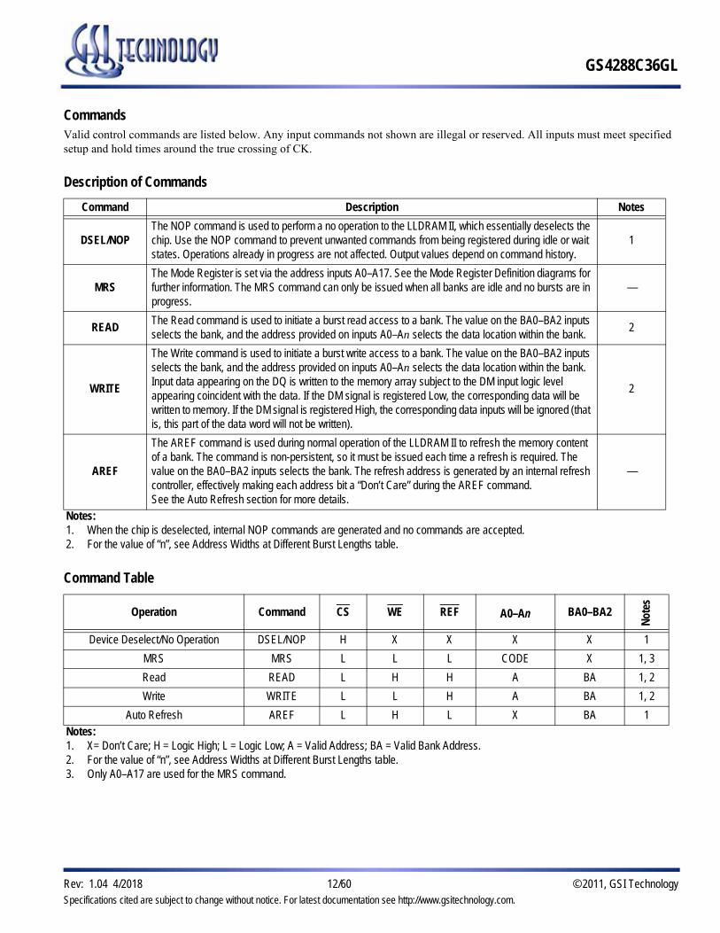
CommandsValid control commands are listed below. Any input commands not shown are illegal or reserved. All inputs must meet specified setup and hold times around the true crossing of CK.
Description of Commands
Command Description Notes
DSEL/NOPThe NOP command is used to perform a no operation to the LLDRAM II, which essentially deselects the chip. Use the NOP command to prevent unwanted commands from being registered during idle or wait states. Operations already in progress are not affected. Output values depend on command history.
1
MRSThe Mode Register is set via the address inputs A0–A17. See the Mode Register Definition diagrams for further information. The MRS command can only be issued when all banks are idle and no bursts are in progress.
—
READThe Read command is used to initiate a burst read access to a bank. The value on the BA0–BA2 inputs selects the bank, and the address provided on inputs A0–An selects the data location within the bank.
2
WRITE
The Write command is used to initiate a burst write access to a bank. The value on the BA0–BA2 inputs selects the bank, and the address provided on inputs A0–An selects the data location within the bank. Input data appearing on the DQ is written to the memory array subject to the DM input logic level appearing coincident with the data. If the DM signal is registered Low, the corresponding data will be written to memory. If the DM signal is registered High, the corresponding data inputs will be ignored (that is, this part of the data word will not be written).
2
AREF
The AREF command is used during normal operation of the LLDRAM II to refresh the memory content of a bank. The command is non-persistent, so it must be issued each time a refresh is required. The value on the BA0–BA2 inputs selects the bank. The refresh address is generated by an internal refresh controller, effectively making each address bit a “Don’t Care” during the AREF command. See the Auto Refresh section for more details.
—
Notes:1. When the chip is deselected, internal NOP commands are generated and no commands are accepted.2. For the value of “n”, see Address Widths at Different Burst Lengths table.
Command Table
Operation Command CS WE REF A0–An BA0–BA2
Not
esDevice Deselect/No Operation DSEL/NOP H X X X X 1
MRS MRS L L L CODE X 1, 3
Read READ L H H A BA 1, 2
Write WRITE L L H A BA 1, 2
Auto Refresh AREF L H L X BA 1Notes:1. X= Don’t Care; H = Logic High; L = Logic Low; A = Valid Address; BA = Valid Bank Address.2. For the value of “n”, see Address Widths at Different Burst Lengths table.3. Only A0–A17 are used for the MRS command.
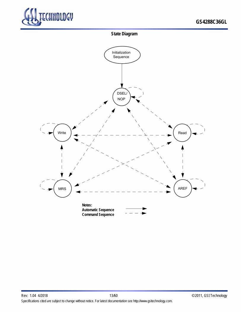
Initialization Sequence
DSEL/
NOP
Read Write
MRS AREF
Notes:Automatic SequenceCommand Sequence
GS4288C36GL
Specifications cited are subject to change without notice. For latest documentation see http://www.gsitechnology.com.
Rev: 1.04 4/2018 13/60 © 2011, GSI Technology
State Diagram

GS4288C36GL
Specifications cited are subject to change without notice. For latest documentation see http://www.gsitechnology.com.
Rev: 1.04 4/2018 14/60 © 2011, GSI Technology
Mode Register SetMode Register Set controls the operating modes of the memory, including configuration, burst length, test mode, and I/O options. During an MRS command, the address inputs A0–A17 are sampled and stored in the Mode Register. Except during initialization to force internal reset, after a valid MRS command, tMRSC must be met before any command except NOP can be issued to the LLDRAM II. All banks must be idle and no bursts may be in progress when an MRS command is loaded.
Note: Changing the burst length configuration may scramble previously written data. A burst length change must be assumed to invalidate all stored data.
Mode Register Set
CODE
CK
CK
CS
WE
REF
Addr
BA(2:0)

M2 M1 M0 Configuration
0 0 0 13 (default)
0 0 1 13
0 1 0 2
0 1 1 3
1 0 0 43
1 0 1 5
1 1 0 Reserved
1 1 1 Reserved
M4 M3Burst
Length
0 0 2 (default)
0 1 4
1 0 8
1 1 Reserved
M5 Address MUX
0 Nonmulitplexed (default)
1 Multiplexed
M7 DLL Reset
0 DLL reset4 (default)
1 DLL enabled
M9On Die
Termination
0 Off (default)
1 On
M8 Drive Impedance
0 Internal 505 (default)
1 External (ZQ)
A10A17 A9 A8 A7 A6 A5 A4 A3 A2 A1 A0...
17–10 9 8 7 6 5 4 3 2 1 0
Reserved1 ODT IM DLL NA2 AM BL Config
Address Bus
Mode Register (Mx)
GS4288C36GL
Specifications cited are subject to change without notice. For latest documentation see http://www.gsitechnology.com.
Rev: 1.04 4/2018 15/60 © 2011, GSI Technology
Mode Register Definition in Nonmultiplexed Address Mode
Notes:1. A10–A17 must be set to zero; A18–An = “Don’t Care”.2. A6 not used in MRS.3. BL = 8 is not available.4. DLL RESET turns the DLL off.5. ±30% over rated temperature range.

GS4288C36GL
Specifications cited are subject to change without notice. For latest documentation see http://www.gsitechnology.com.
Rev: 1.04 4/2018 16/60 © 2011, GSI Technology
Configuration TablesThe relationship between cycle time and read/write latency is selected by the user. The configuration table below lists valid configurations available via Mode Register bits M0, M1, and M2 and the clock frequencies supported for each setting. Write Latency is equal to the Read Latency plus one in each configuration to reduce bus conflicts.
Cycle Time and Read/Write Latency Configuration Table
ParameterConfiguration
Units12 2 3 42, 3 5
tRC 4 6 8 3 5 tCK
tRL 4 6 8 3 5 tCK
tWL 5 7 9 4 6 tCK
Valid Frequency Range 266–175 400–175 533–175 200–175 333–175 MHzNotes:1. tRC < 20 ns in any configuration is only available with –18 and –24 speed grades.2. BL = 8 is not available. 3. The minimum tRC is typically 3 cycles, except in the case of a Write followed by a Read to the same bank. In this instance, the minimum
tRC is 4 cycles.

GS4288C36GL
Specifications cited are subject to change without notice. For latest documentation see http://www.gsitechnology.com.
Rev: 1.04 4/2018 17/60 © 2011, GSI Technology
Burst Length Read and Write data transfers occur in bursts of 2, 4, or 8 beats. Burst Length is programmed by the user via Mode Register Bit 3 (M3) and Bit 4 (M4). The Read Burst Length diagrams illustrate the different burst lengths with respect to a Read Command. Changes in the burst length affect the width of the address bus.
Note: Changing the burst length configuration may scramble previously written data. A burst length change must be assumed to invalidate all stored data.
Read Burst Lengths
READ
Q0 Q1
READ NOP NOP NOP NOP NOP NOP NOP
Q0 Q1 Q2 Q3
READ NOP NOP NOP NOP NOP NOP NOP
Q0 Q1 Q2 Q3 Q4 Q5 Q6 Q7
RL = 5
RL = 5
RL = 5
Example BL=2
Example BL=4
Example BL=8
CK
CK
Command
QKx
QKx
QVLD
DQ
CK1
CK1
Command1
QKx1
QKx1
QVLD1
DQ1
CK2
CK2
Command2
QKx2
QKx2
QVLD2
DQ2
Address Widths at Different Burst Lengths
Burst Length Configuration
x36
2 A0–A18
4 A0–A17
8 A0–A16

GS4288C36GL
Specifications cited are subject to change without notice. For latest documentation see http://www.gsitechnology.com.
Rev: 1.04 4/2018 18/60 © 2011, GSI Technology
WriteWrite data transfers are launched with a Write command, as shown below. A valid address must be provided during the Write command.
During Write data transfers, each beat of incoming data is registered on crossings of DK and DK until the burst transfer is complete. Write Latency (WL) that is always one cycle longer than the programmed Read Latency (RL), so the first valid data registered at the first True crossing of the DK clocks WL cycles after the Write command.
A Write burst may be followed by a Read command (assuming tRC is met). At least one NOP command is required between Write and Read commands to avoid data bus contention. The Write-to-Read timing diagrams illustrate the timing requirements for a Write followed by a Read. Setup and hold times for incoming DQ relative to the DK edges are specified as tDS and tDH. Input data may be masked a High on an associated DM pin. The setup and hold times for the DM signal are tDS and tDH.W
Write Command
A
BA
CK
CK
CS
WE
REF
Addr
BA(2:0)

GS4288C36GL
Specifications cited are subject to change without notice. For latest documentation see http://www.gsitechnology.com.
Rev: 1.04 4/2018 19/60 © 2011, GSI Technology
Write Burst Length 2, Configuration 1
T0 T1 T2 T3 T4 T5 T6 T7 T8
WR WR WR WR WR WR WR WR WR
A A A A A A A A A
BA0 BA1 BA2 BA3 BA0 BA4 BA5 BA6 BA7
D0a D0b D1a D1b D2a D2b D3a D3b
WL=5
RC = 4RC = 4
CK
CK
CMD
ADDR
BA
DK
DK
DM
DQ
Write Burst Length 4, Configuration 1
T0 T1 T2 T3 T4 T5 T6 T7 T8
WR NOP WR NOP WR NOP WR NOP WR
A A A A A
BA0 BA1 BA0 BA3 BA0
D0a D0b D0c D0d D1a D1b D1c D1d
WL = 5
RC = 4RC = 4
CK
CK
CMD
ADDR
BA
DK
DK
DM
DQ

GS4288C36GL
Specifications cited are subject to change without notice. For latest documentation see http://www.gsitechnology.com.
Rev: 1.04 4/2018 20/60 © 2011, GSI Technology
Write-Read Burst Length 2, Configuration 1
0 1 2 3 4 5 6 7 8 9
WR NOP RD RD NOP NOP NOP NOP NOP NOP
A A A
BA0 BA1 BA2
D0a D0b Q1a Q1b Q2a Q2b
WL = 5
RL = 4
CK
CK
CMD
ADDR
BA
DK
DK
DM
DQ
QVLD
QKx
QKx

GS4288C36GL
Specifications cited are subject to change without notice. For latest documentation see http://www.gsitechnology.com.
Rev: 1.04 4/2018 21/60 © 2011, GSI Technology
Write-Read Burst Length 4, Configuration 1
T0 T1 T2 T3 T4 T5 T6 T7 T8 T9
WR NOP NOP RD NOP RD NOP NOP NOP NOP
A A A
BA0 BA1 BA2
D0a D0b D0c D0d Q1a Q1b Q1c Q1d Q2a
WL = 5
RL = 4
CK
CK
CMD
ADDR
BA
DK
DK
DM
DQ
QVLD
QKx
QKx
GS4288C36GL
Specifications cited are subject to change without notice. For latest documentation see http://www.gsitechnology.com.
Rev: 1.04 4/2018 22/60 © 2011, GSI Technology
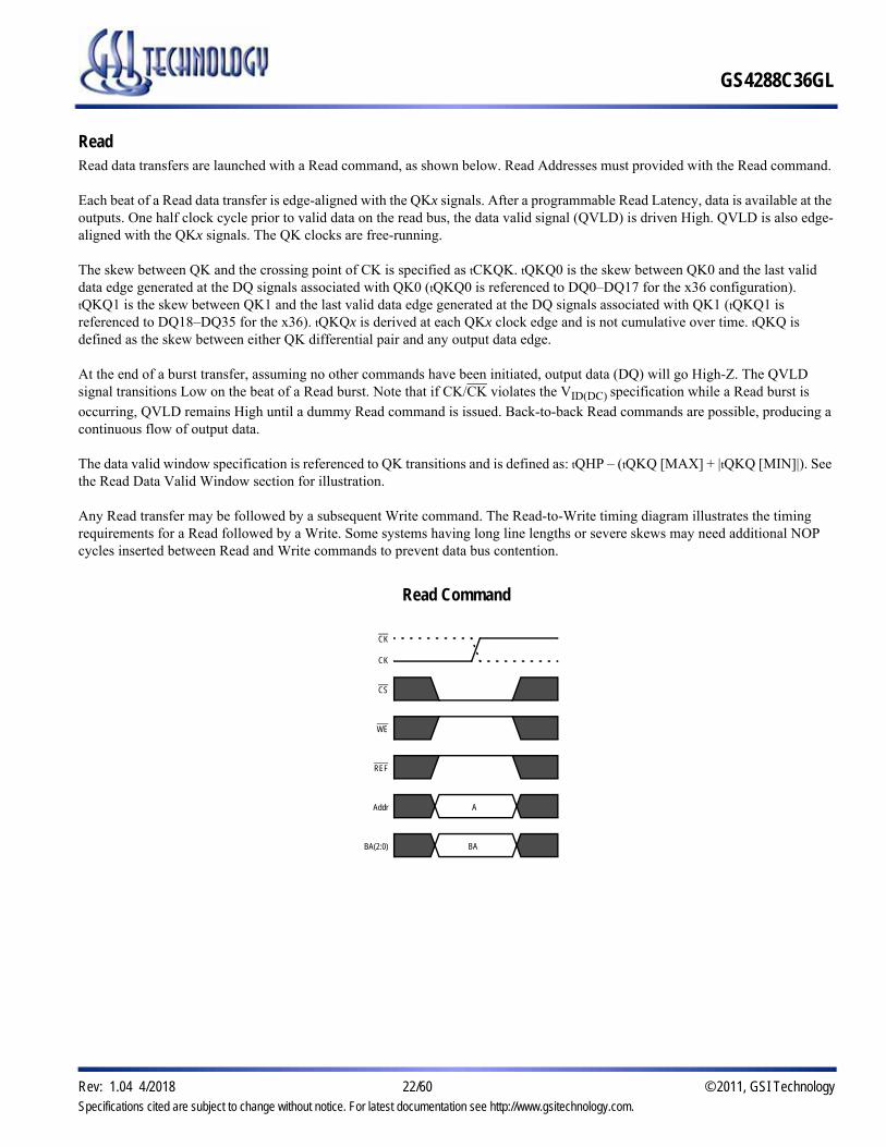
Read Read data transfers are launched with a Read command, as shown below. Read Addresses must provided with the Read command.
Each beat of a Read data transfer is edge-aligned with the QKx signals. After a programmable Read Latency, data is available at the outputs. One half clock cycle prior to valid data on the read bus, the data valid signal (QVLD) is driven High. QVLD is also edge-aligned with the QKx signals. The QK clocks are free-running.
The skew between QK and the crossing point of CK is specified as tCKQK. tQKQ0 is the skew between QK0 and the last valid data edge generated at the DQ signals associated with QK0 (tQKQ0 is referenced to DQ0–DQ17 for the x36 configuration). tQKQ1 is the skew between QK1 and the last valid data edge generated at the DQ signals associated with QK1 (tQKQ1 is referenced to DQ18–DQ35 for the x36). tQKQx is derived at each QKx clock edge and is not cumulative over time. tQKQ is defined as the skew between either QK differential pair and any output data edge.
At the end of a burst transfer, assuming no other commands have been initiated, output data (DQ) will go High-Z. The QVLD signal transitions Low on the beat of a Read burst. Note that if CK/CK violates the VID(DC) specification while a Read burst is
occurring, QVLD remains High until a dummy Read command is issued. Back-to-back Read commands are possible, producing a continuous flow of output data.
The data valid window specification is referenced to QK transitions and is defined as: tQHP – (tQKQ [MAX] + |tQKQ [MIN]|). See the Read Data Valid Window section for illustration.
Any Read transfer may be followed by a subsequent Write command. The Read-to-Write timing diagram illustrates the timing requirements for a Read followed by a Write. Some systems having long line lengths or severe skews may need additional NOP cycles inserted between Read and Write commands to prevent data bus contention.
Read Command
A
BA
CK
CK
CS
WE
REF
Addr
BA(2:0)
GS4288C36GL
Specifications cited are subject to change without notice. For latest documentation see http://www.gsitechnology.com.
Rev: 1.04 4/2018 23/60 © 2011, GSI Technology
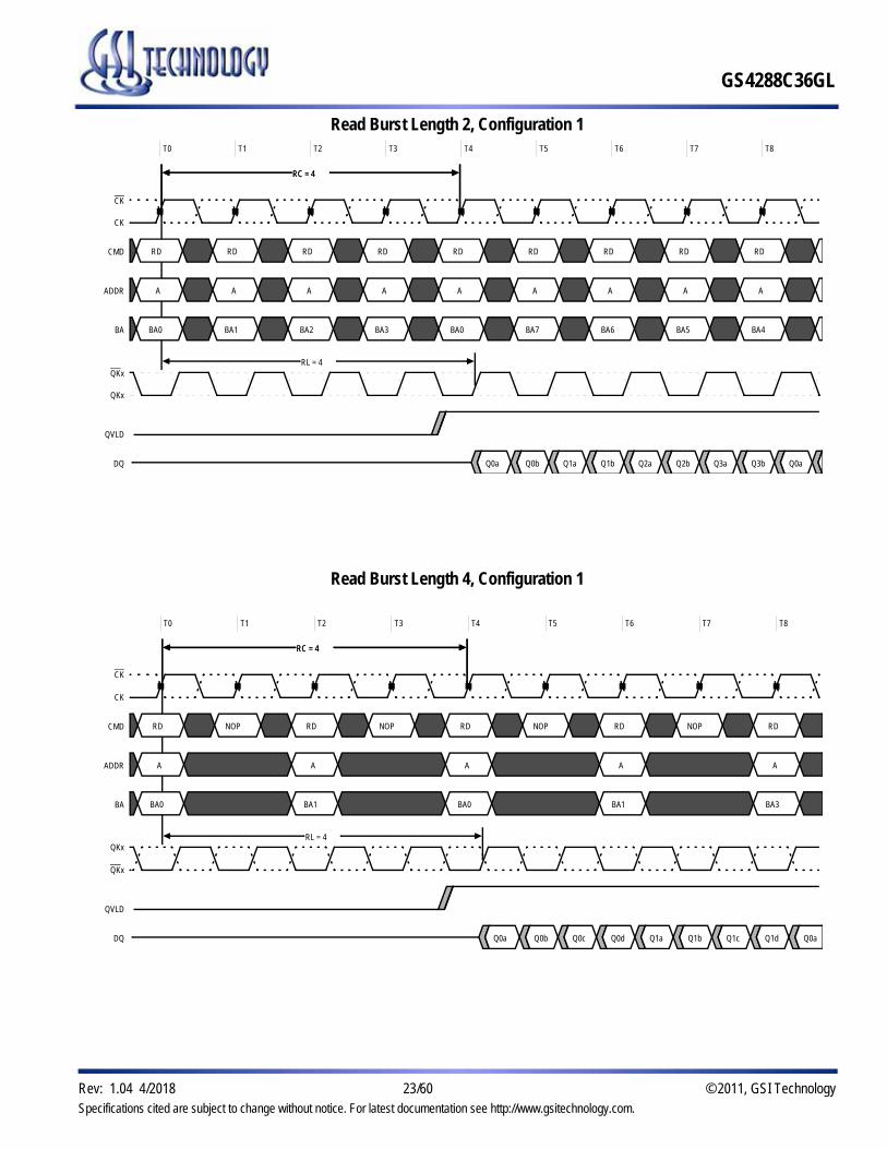
Read Burst Length 2, Configuration 1T0 T1 T2 T3 T4 T5 T6 T7 T8
RD RD RD RD RD RD RD RD RD
A A A A A A A A A
BA0 BA1 BA2 BA3 BA0 BA7 BA6 BA5 BA4
Q0a Q0b Q1a Q1b Q2a Q2b Q3a Q3b Q0a
RL = 4
RC = 4RC = 4
CK
CK
CMD
ADDR
BA
QKx
QKx
QVLD
DQ
Read Burst Length 4, Configuration 1
T0 T1 T2 T3 T4 T5 T6 T7 T8
RD NOP RD NOP RD NOP RD NOP RD
A A A A A
BA0 BA1 BA0 BA1 BA3
Q0a Q0b Q0c Q0d Q1a Q1b Q1c Q1d Q0a
RL = 4
RC = 4RC = 4
CK
CK
CMD
ADDR
BA
QKx
QKx
QVLD
DQ
GS4288C36GL
Specifications cited are subject to change without notice. For latest documentation see http://www.gsitechnology.com.
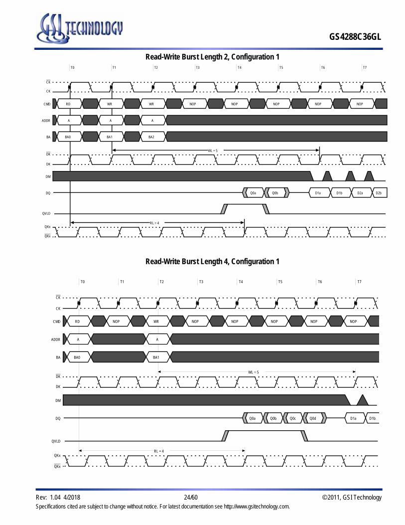
Rev: 1.04 4/2018 24/60 © 2011, GSI Technology
Read-Write Burst Length 2, Configuration 1T0 T1 T2 T3 T4 T5 T6 T7
RD WR WR NOP NOP NOP NOP NOP
A A A
BA0 BA1 BA2
Q0a Q0b D1a D1b D2a D2b
RL = 4
WL = 5
CK
CK
CMD
ADDR
BA
DK
DK
DM
DQ
QVLD
QKx
QKx
Read-Write Burst Length 4, Configuration 1
T0 T1 T2 T3 T4 T5 T6 T7
RD NOP WR NOP NOP NOP NOP NOP
A A
BA0 BA1
Q0a Q0b Q0c Q0d D1a D1b
RL = 4
WL = 5
CK
CK
CMD
ADDR
BA
DK
DK
DM
DQ
QVLD
QKx
QKx

GS4288C36GL
Specifications cited are subject to change without notice. For latest documentation see http://www.gsitechnology.com.
Rev: 1.04 4/2018 25/60 © 2011, GSI Technology
Auto Refresh The Auto Refresh (AREF) command launches a REFRESH cycle on one row in the bank addressed. Refresh row addresses are generated by an internal refresh counter, so address inputs are Don’t Care, but a bank addresses (BA 2:0) must be provided during the AREF command. A refresh may be contining in one bank while other commands, including other AREF commands, are launched in other banks. The delay between the AREF command and a READ, WRITE or AREF command to the same bank must be at least tRC.
The entire memory must be refreshed every 32 ms (tREF). This means that this 288Mb device requires 64K refresh cycles at an average periodic interval of 0.49s MAX (actual periodic refresh interval is 32 ms/8K rows/8 banks = 0.488s). To improve efficiency, eight AREF commands (one for each bank) can be launched at periodic intervals of 3.90s (32 ms/8K rows = 3.90s). The Auto Refresh Cycle diagram illustrates an example of a refresh sequence.
Auto Refresh (AREF) Command
BA
CK
CK
CS
WE
REF
A(20:0)
BA(2:0)
Auto Refresh Cycle
AREF AREF NOP AREF
BA0 BA3 BA4
CK
CK
CMD
Bank

GS4288C36GL
Specifications cited are subject to change without notice. For latest documentation see http://www.gsitechnology.com.
Rev: 1.04 4/2018 26/60 © 2011, GSI Technology
Address MultiplexingLLDRAM II defaults to “broadside” addressing at power up, meaning, it registers all address inputs on a single clock transition. However, for most configurations of the device, considerable efficiency can be gained by operating in Address Multiplexed mode, cutting the address pin count on the host device in half. In Multiplexed Address mode, the address is loaded in two consecutive clock transitions. Broadside Addressing only improves Continuous Burst mode data transfer efficiency of Burst Length 2 (BL = 2) configuration.
In Address Multiplex mode, bank addresses are loaded on the same clock transition as Command and the first half of the address, Ax. The 576Mb Address Mapping in Multiplexed Address Mode table and Cycle Time and Read/Write Latency Configuration in Mulitplexed Mode table show the addresses needed for both the first and second clock transitions (Ax and Ay, respectively). The AREF command does not require an address on the second clock transition, as only the Bank Address are loaded for refresh commands. Therefore, AREF commands may be issued on consecutive clocks, even when in Address Multiplex mode.
Setting Mode Register Bit 5 (M5) to 1 in the Mode Register activates the Multiplexed Address mode. Once this bit is set subsequent MRS, READ, and WRITE operate as described in the Multiplexed Address Mode diagram.

GS4288C36GL
Specifications cited are subject to change without notice. For latest documentation see http://www.gsitechnology.com.
Rev: 1.04 4/2018 27/60 © 2011, GSI Technology
Power-Up Multiplexed Address Mode
200us Min tMRSC tMRSC Refresh All Banks(9) 1024 NOP cycles Min
NOP NOP MRS MRS MRS NOP MRS NOP REF REF NOP AC
CODE(1,2) CODE(1,2) CODE(2,3) Ax(2,4) Ay(2) Valid(5)
Bank 0 Bank 7 Valid(5)
tDKL
tDK
tDKLtDKHtDKH
tDK
tCKLtCK
tCKLtCKHtCKH
tCK
VEXT
VDD
VDDQ
VREF
VTT
CK
CK
DK
DK
Command
ADDR
Bank

GS4288C36GL
Specifications cited are subject to change without notice. For latest documentation see http://www.gsitechnology.com.
Rev: 1.04 4/2018 28/60 © 2011, GSI Technology
MRS Command In Multiplexed ModeThe Mode Register Set command stores the data for controlling the RAM into the Mode Register. The register allows the user to modify Read and Write pipeline length, burst length, test mode, and I/O options. The Multiplexed MRS command requires two cycles to complete The Ax address is sampled on the true crossing of clock with the MRS Command. The Ay address and a required NOP command are captured on the next next crossing of clock. After issuing a valid MRS command, tMRSC must be met before any READ, WRITE, MRS, or AREF command can be issued to the LLDRAM II. This statement does not apply to the consecutive MRS commands needed for internal logic reset during the initialization routine. The MRS command can only be issued when all banks are idle and no bursts are in progress.
Note: The data written by the prior burst length is not guaranteed to be accurate when the burst length of the device is changed.
MRS Command in Multiplexed Mode
MRS
Ax Ay
CK
CK
CS
WE
REF
A(20:0)
BA(2:0)
Notes:1. Recommended that all address pins held Low during dummy MRS commands.2. A10–A18 must be Low.3. Set address A5 High. This enbles the part to enter Multiplexed Address mode when in Non-Multiplexed mode operation. Multiplexed
Address mode can also be entered at some later time by issuing an MRS command with A5 High. Once address Bit A5 is set High, tMRSC must be satisfied before the two-cycle multiplexed mode MRS command is issued.
4. Address A5 must be set High. This and the following step set the desired mode register once the LLDRAM II is in Multiplexed Address mode.
5. Any command or address.6. The above sequence must be followed in order to power up the LLDRAM II in the Multiplexed Address mode.7. DLL must be reset if tCK or VDD are changed.8. CK and CK must separated at all times to prevent bogus commands from being issued.9. The sequence of the eight AUTO REFRESH commands (with respect to the 1024 NOP commands) does not matter. As is required for any
operation, tRC must be met between an AUTO REFRESH command and a subsequent VALID command to the same bank.

GS4288C36GL
Specifications cited are subject to change without notice. For latest documentation see http://www.gsitechnology.com.
Rev: 1.04 4/2018 29/60 © 2011, GSI Technology
Mode Register Definition in Multiplexed Address Mode
M2 M1 M0 Configuration
0 0 0 12 (default)
0 0 1 12
0 1 0 2
0 1 1 3
1 0 0 42
1 0 1 5
1 1 0 Reserved
1 1 1 Reserved
M4 M3Burst
Length
0 0 2 (default)
0 1 4
1 0 8
1 1 Reserved
M5 Address MUX
0 Nonmulitplexed (default)
1 Multiplexed
M7 DLL Reset
0 DLL reset4 (default)
1 DLL enabled
M9On Die
Termination
0 Off (default)
1 On
M8 Drive Impedance
0 Internal 503 (default)
1 External (ZQ)
A18...A10 A9 A8 A4 A3
18–10 9 8 7 6 5 4 3 2 1 0
Reserved1 ODT IM DLL NA5 AM BL Config Mode Register (Mx)
A18...A10 A9 A8 A5 A4 A3 A0
Ay Ax
Notes:1. A10–A18 must be set to zero.2. BL = 8 is not available.3. ±30% over rated temperature range.4. DLL RESET turns the DLL off.5. Ay8 not used in MRS.6. BA0–BA2 are “Don’t Care”.7. Addresses A0, A3, A4, A5, A8, and A9 must be set as shown in order to activate the Mode Register in the Multiplexed Address mode.

288Mb Address Mapping in Multiplexed Address Mode
Data WidthBurst
LengthBall
Address
A0 A3 A4 A5 A8 A9 A10 A13 A14 A17 A18
x36
2Ax A0 A3 A4 A5 A8 A9 A10 A13 A14 A17 A18
Ay X A1 A2 X A6 A7 X A11 A12 A16 A15
4Ax A0 A3 A4 A5 A8 A9 A10 A13 A14 A17 X
Ay X A1 A2 X A6 A7 X A11 A12 A16 A15
8Ax A0 A3 A4 A5 A8 A9 A10 A13 A14 X X
Ay X A1 A2 X A6 A7 X A11 A12 A16 A15Notes:X = Don’t Care.
GS4288C36GL
Specifications cited are subject to change without notice. For latest documentation see http://www.gsitechnology.com.
Rev: 1.04 4/2018 30/60 © 2011, GSI Technology
Configuration in Mulitplexed ModeIn Multiplexed Address mode, the Read and Write latencies are increased by one clock cycle. However, the LLDRAM II cycle time remains the same as when in Nonmultiplexed Address mode.
Cycle Time and Read/Write Latency Configuration in Mulitplexed Mode
ParameterConfiguration
Units12 2 3 42, 3 5
tRC 4 6 8 3 5 tCK
tRL 5 7 9 4 6 tCK
tWL 6 8 10 5 7 tCK
Valid Frequency Range 266–175 400–175 533–175 200–175 333–175 MHzNotes: 1. tRC < 20 ns in any configuration is only available with –24 and –18 speed grades.2. BL = 8 is not available.3. The minimum tRC is typically 3 cycles, except in the case of a Write followed by a Read to the same bank. In this instance the minimum
tRC is 4 cycles.
Write Command in Multiplexed ModeAddress Multiplexed Write data transfers are launched with a Write command, as shown below. A valid address must be provided during the Write command. The Ax address must be loaded on the same true clock crossing used to load the Write command and the Bank address. The Ay address and a NOP command must be provided at the next clock crossing.
During Write data transfers, each beat of incoming data is registered on crossings of DK and DK until the burst transfer is complete. Write Latency (WL) is always one cycle longer than the programmed Read Latency (RL).
A Write burst may be followed by a Read command (assuming tRC is met). At least one NOP command is required between Write and Read commands to avoid data bus contention. The Write-to-Read timing diagrams illustrate the timing requirements for a Write followed by a Read. Setup and hold times for incoming DQ relative to the DK edges are specified as tDS and tDH. Input data may be masked high on an associated DM pin. The setup and hold times for the DM signal are tDS and tDH.

GS4288C36GL
Specifications cited are subject to change without notice. For latest documentation see http://www.gsitechnology.com.
Rev: 1.04 4/2018 31/60 © 2011, GSI Technology
Write Command in Multiplexed ModeWRITE
Ax Ay
BA
CK
CK
CS
WE
REF
A(20:0)
BA(2:0)
Write Burst Length 4, Configuration 1 in Multiplexed Mode
T0 T1 T2 T3 T4 T5 T6 T7 T8
WR NOP WR NOP WR NOP WR NOP WR
Ax Ay Ax Ay Ax Ay Ax Ay Ax
BA0 BA1 BA0 BA3 BA0
D0a D0b D0c D0d D1a D1b
WL = 6
RC = 4RC = 4
CK
CK
CMD
ADDR
BA
DK
DK
DM
D
Read Command in Multiplexed ModeAddress Multiplexed Read data transfers are launched with a Read command, as shown below. A valid address must be provided during the READ command. The Ax address must be loaded on the same True clock crossing used to load the READ command and the Bank address. The Ay address and a NOP command must be provided at the next clock crossing.
Each beat of a Read data transfer is edge-aligned with the QKx signals. After a programmable Read Latency, data is available at the outputs. One half clock cycle prior to valid data on the read bus, the data valid signal (QVLD) is driven High. QVLD is also edge-aligned with the QKx signals. The QK clocks are free-running.

GS4288C36GL
Specifications cited are subject to change without notice. For latest documentation see http://www.gsitechnology.com.
Rev: 1.04 4/2018 32/60 © 2011, GSI Technology
The skew between QK and the crossing point of CK is specified as tCKQK. tQKQ0 is the skew between QK0 and the last valid data edge generated at the DQ signals associated with QK0 (tQKQ0 is referenced to DQ0–DQ17 for the x36 configuration). tQKQ1 is the skew between QK1 and the last valid data edge generated at the DQ signals associated with QK1 (tQKQ1 is referenced to DQ18–DQ35 for the x36). tQKQx is derived at each QKx clock edge and is not cumulative over time. tQKQ is defined as the skew between either QK differential pair and any output data edge.
At the end of a burst transfer, assuming no other commands have been initiated, output data (DQ) will go High–Z. The QVLD signal transitions Low on the beat of a Read burst. Note that if CK/CK violates the VID(DC) specification while a Read burst is
occurring, QVLD remains High until a dummy Read command is issued. Back-to-back Read commands are possible, producing a continuous flow of output data.
The data valid window specification is referenced to QK transitions and is defined as: tQHP – (tQKQ [MAX] + |tQKQ [MIN]|). See the Read Data Valid Window section.
Any Read transfer may be followed by a subsequent Write command. The Read-to-Write timing diagram illustrates the timing requirements for a Read followed by a Write. Some systems having long line lengths or severe skews may need additional NOP cycles inserted between Read and Write commands to prevent data bus contention.
Read Command in Mulitplexed ModeREAD
Ax Ay
BA
CK
CK
CS
WE
REF
A(20:0)
BA(2:0)
GS4288C36GL
Specifications cited are subject to change without notice. For latest documentation see http://www.gsitechnology.com.
Rev: 1.04 4/2018 33/60 © 2011, GSI Technology
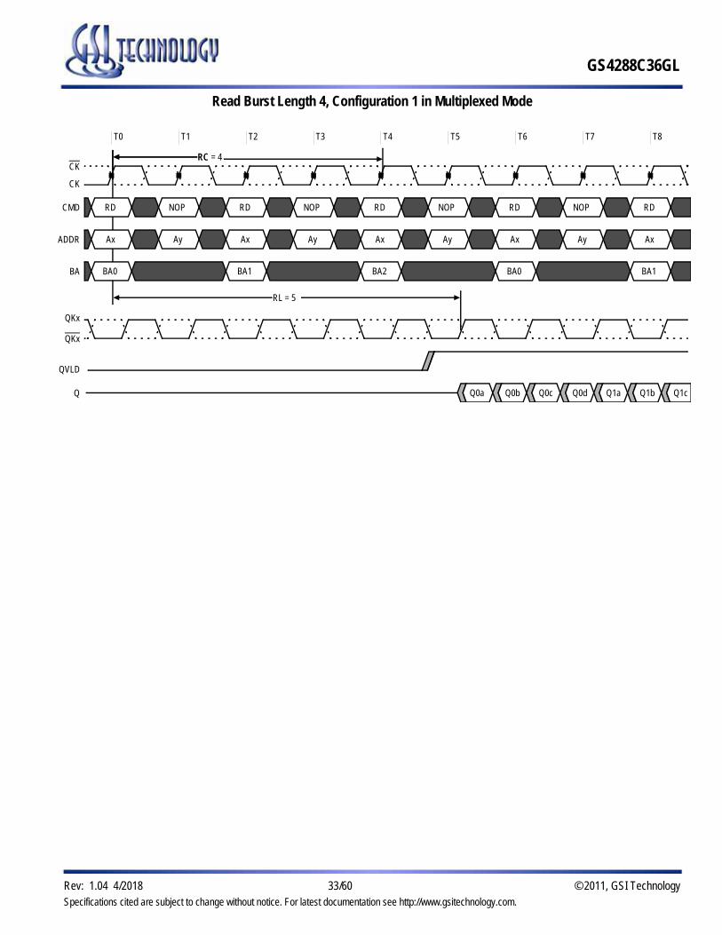
Read Burst Length 4, Configuration 1 in Multiplexed Mode
T0 T1 T2 T3 T4 T5 T6 T7 T8
RD NOP RD NOP RD NOP RD NOP RD
Ax Ay Ax Ay Ax Ay Ax Ay Ax
BA0 BA1 BA2 BA0 BA1
Q0a Q0b Q0c Q0d Q1a Q1b Q1c
RL = 5
RC RC = 4
CK
CK
CMD
ADDR
BA
QKx
QKx
QVLD
Q

GS4288C36GL
Specifications cited are subject to change without notice. For latest documentation see http://www.gsitechnology.com.
Rev: 1.04 4/2018 34/60 © 2011, GSI Technology
Refresh Commands in Multiplexed Address ModeThe AREF command launches a REFRESH cycle on one row in the bank addressed. Refresh row addresses are generated by an internal refresh counter. so address inputs are Don’t Care, but Bank addresses (BA 2:0) must be provided during the AREF command. A refresh may be continuing in one bank while other commands, including other AREF commands, are launched in other banks. The delay between the AREF command and a READ, WRITE or AREF command to the same bank must be at least tRC.
The entire memory must be refreshed every 32 ms (tREF). This means that this 576Mb device requires 128K refresh cycles at an average periodic interval of 0.24s MAX (actual periodic refresh interval is 32 ms/16K rows/8 = 0.244s). To improve efficiency, eight AREF commands (one for each bank) can be launched at periodic intervals of 1.95s (32 ms/16K rows = 1.95s). The Auto Refresh Cycle diagram illustrates an example of a refresh sequence.
Unlike READ and WRITE commands in Address Multiplex mode, all the information needed to execute an AREF command (the AREF command and the Band Address (BA 2:0)) is loaded in a single clock crossing, another AREF command (to a different bank) may be loaded on the next clock crossing.
Consecutive Refresh Operations with Multiplexed Mode
T0 T1 T2 T3 T4 T5 T6 T7 T8 T9 T10 T11
AC NOP AREF AREF AREF AREF AREF AREF AREF AREF AC NOP
Ax Ay Ax Ay
BAn BA0 BA1 BA2 BA3 BA4 BA5 BA6 BA7 BAn
CK
CK
CMD
ADDR
BA
Notes:1. Any command.2. Bank n is chosen so that tRC is met.

GS4288C36GL
Specifications cited are subject to change without notice. For latest documentation see http://www.gsitechnology.com.
Rev: 1.04 4/2018 35/60 © 2011, GSI Technology
Absolute Maximum Ratings
Absolute Maximum Voltage(All voltages reference to VSS)
Parameter Min Max Unit
I/O Voltage –0.3 VDDQ + 0.3 V
Voltage on VEXT supply –0.3 +2.8 V
Voltage on VDD supply relative to VSS –0.3 +2.1 V
Voltage on VDDQ supply relative to VSS –0.3 +2.1 V
Note: Permanent damage to the device may occur if the Absolute Maximum Ratings are exceeded. Operation should be restricted to Recommended Operating Conditions. Exposure to conditions exceeding the Absolute Maximum Ratings, for an extended period of time, may affect reliability of this component.
Absolute Maximum Temperature
Parameter Temperature
RangeSymbol Min. Max. Unit Notes
Storage Temperature — TSTG –55 +150 C° 1
Reliability junction temperatureCommercial
TJ— +110 C° 2
Industrial — +110 C° 2
Notes:1. Max storage case temperature; TSTG is measured in the center of the package. 2. Temperatures greater than 110 C° may cause permanent damage to the device. This is a stress rating only and functional operation of the
device at or above this is not implied. Exposure to the absolute maximum ratings conditions for extended periods may affect reliability of the part.

GS4288C36GL
Specifications cited are subject to change without notice. For latest documentation see http://www.gsitechnology.com.
Rev: 1.04 4/2018 36/60 © 2011, GSI Technology
Recommended Operating Temperature and Thermal ImpedanceLike any other semiconductor device, the LLDRAM II must be operated within the temperature specifications shown in the Temperature Limits table for the device to meet datasheet specifications. The thermal impedance characteristics of the device are listed below. In applications where the ambient temperature or PCB temperature are too high, use of forced air and/or heat sinks may be required in order to satisfy the case temperature specifications.
Temperature Limits
Parameter Temperature
RangeSymbol Min. Max. Unit Notes
Operating junction temperatureCommercial
TJ0 +100 C° 1
Industrial –40 +100 C° 1
Operating case temperatureCommercial
TC0 +95 C° 2, 3
Industrial –40 +95 C° 2, 3, 4
Notes:1. Junction temperature depends upon package type, cycle time, loading, ambient temperature, and airflow. 2. Maximum operating case temperature, TC, is measured in the center of the package.3. Device functionality is not guaranteed if the device exceeds maximum TC during operation.4. Junction and case temperature specifications must be satisfied.
Thermal Impedance
PackageTest PCBSubstrate
JA (C°/W)Airflow = 0 m/s
JA (C°/W)Airflow = 1 m/s
JA (C°/W)Airflow = 2 m/s
JB (C°/W) JC (C°/W)
BGA 2-layer 29.0 21.9 19.9 13.6 4.0
4-layer 18.5 13.5 12.6 12.4 4.2
Notes:1. Thermal Impedance data is based on a number of of samples from mulitple lots and should be viewed as a typical number. 2. Please refer to JEDEC standard JESD51-6. 3. The characteristics of the test fixture PCB influence reported thermal characteristics of the device. The minimal metalization of a 2-layer
board tends to minimize the utility of the junction-to-board heat path. The 4-layer test fixture PCB is intended to highlight the effect of connection to power planes typically found in the PCBs used in most applications. Be advised that a good thermal path to the PCB can result in cooling or heating of the RAM depending on PCB temperature.
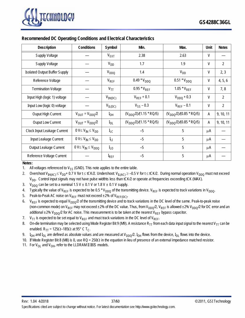
Recommended DC Operating Conditions and Electrical Characteristics
Description Conditions Symbol Min. Max. Unit Notes
Supply Voltage — VEXT 2.38 2.63 V —
Supply Voltage — VDD 1.7 1.9 V 2
Isolated Output Buffer Supply — VDDQ 1.4 VDD V 2, 3
Reference Voltage — VREF 0.49 * VDDQ 0.51 * VDDQ V 4, 5, 6
Termination Voltage — VTT 0.95 * VREF 1.05 * VREF V 7, 8
Input High (logic 1) voltage — VIH(DC) VREF + 0.1 VDDQ + 0.3 V 2
Input Low (logic 0) voltage — VIL(DC) VSS – 0.3 VREF – 0.1 V 2
Ouput High Current VOUT = VDDQ/2 IOH (VDDQ/2)/(1.15 * RQ/5) (VDDQ/2)/(0.85 * RQ/5) A 9, 10, 11
Ouput Low Current VOUT = VDDQ/2 IOL (VDDQ/2)/(1.15 * RQ/5) (VDDQ/2)/(0.85 * RQ/5) A 9, 10, 11
Clock Input Leakage Current 0 V VIN VDD ILC –5 5 A —
Input Leakage Current 0 V VIN VDD ILI –5 5 A —
Output Leakage Current 0 V VIN VDDQ ILO –5 5 A —
Reference Voltage Current — IREF –5 5 A —
Notes:1. All voltages referenced to VSS (GND). This note applies to the entire table. 2. Overshoot VIH(AC) VDD+ 0.7 V for t tCK/2. Undershoot: VIL(AC) –0.5 V for t tCK/2. During normal operation VDDQ must not exceed
VDD. Control input signals may not have pulse widthts less than tCK/2 or operate at frequencies exceeding tCK (MAX).3. VDDQ can be set to a nominal 1.5 V ± 0.1 V or 1.8 V ± 0.1 V supply.4. Typically the value of VREF is expected to be 0.5 * VDDQ of the transmitting device. VREF is expected to track variations in VDDQ. 5. Peak-to-Peak AC noise on VREF must not exceed ±2% of VREF(DC).6. VREF is expected to equal VDDQ/2 of the transmitting device and to track variations in the DC level of the same. Peak-to-peak noise
(non-common mode) on VREF may not exceed ±2% of the DC value. Thus, from VDDQ/2, VREF is allowed ±2% VDDQ/2 for DC error and an addtional ±2% VDDQ/2 for AC noise. This measurement is to be taken at the nearest VREF bypass capacitor.
7. VTT is expected to be set equal to VREF and must track variations in the DC level of VREF.8. On-die termination may be selected using Mode Register Bit 9 (M9). A resistance RTT from each data input signal to the nearest VTT can be
enabled. RTT = 125–185at 95° C TC.9. IOH and IOL are defined as absolute values and are measured at VDDQ/2. IOH flows from the device, IOL flows into the device.10. If Mode Register Bit 8 (M8) is 0, use RQ = 250in the equation in lieu of presence of an external impedance matched resistor.11. For VOL and VOH, refer to the LLDRAM II IBIS models.
GS4288C36GL
Specifications cited are subject to change without notice. For latest documentation see http://www.gsitechnology.com.
Rev: 1.04 4/2018 37/60 © 2011, GSI Technology

GS4288C36GL
Specifications cited are subject to change without notice. For latest documentation see http://www.gsitechnology.com.
Rev: 1.04 4/2018 38/60 © 2011, GSI Technology
DC Differential Input Clock Logic Levels
Parameter Symbol Min. Max. Unit Notes
Clock input voltage level: CK and CK VIN(DC) –0.3 VDDQ + 0.3 V 1–4
Clock input differential voltage: CK and CK VID(DC) 0.2 VDDQ + 0.6 V 1–5
Notes:1. DKx and DKx have the same requirements as CK and CK. 2. All voltages referenced to VSS (GND).3. The CK and CK input reference level (for timing referenced to CK/CK) is the point at which CK and CK cross. The input reference level for
signals other than CK/CK is VREF.4. The CK and CK input slew rate must be 2 V/ns ( 4 V/ns if measured differentially).5. VID is the magnitude of the difference between the input level on CK and the input level on CK.
Recommended AC Operating Conditions and Electrical Characteristics
Input AC Logic Levels
Parameter Symbol Min. Max. Unit Notes
Input High (logic 1) Voltage VIH VREF + 0.2 — V 1, 2, 3
Input Low (logic 0) Voltage VIL — VREF – 0.2 V 1, 2, 3
Notes:1. All voltages referenced to VSS (GND).2. The AC and the DC input level specifications are defined in the HSTL standard (that is, the receiver will effectively switch as a result of the
signal crossing the AC input level, and will remain in that state as long as the signal does not ring back above (see drawing below) the DC input Low (High) level).
3. The minimum slew rate for the input signals used to test the device is 2 V/ns in the range between VIL(AC) and VIH(AC).
VIH(DC)MIN
VREF
VIL(DC)MAX
VDDQ
VIH(AC)MIN
VIL(AC)MAX
VSS
VS
WIN
G(A
C) (
MIN
)
Nominal tAS/ tCS/ tDS and tAH/ tCH/ tDH Slew Rate

GS4288C36GL
Specifications cited are subject to change without notice. For latest documentation see http://www.gsitechnology.com.
Rev: 1.04 4/2018 39/60 © 2011, GSI Technology
AC Differential Input Clock Levels
Parameter Symbol Min. Max. Unit Notes
Clock input differential voltage: CK and CK VID(AC) 0.4 VDDQ + 0.6 V 1–5
Clock input crossing point voltage: CK and CK VIX(AC) VDDQ/2 – 0.15 VDDQ/2 + 0.15 V 1–4, 6
Notes:1. DKx and DKx have the same requirements as CK and CK. 2. All voltages referenced to VSS (GND).3. The CK and CK input reference level (for timing referenced to CK/CK) is the point at which CK and CK cross. The input reference level for
signals other than CK/CK is VREF.4. The CK and CK input slew rate must be 2 V/ns ( 4 V/ns if measured differentially).5. VID is the magnitude of the difference between the input level on CK and the input level on CK. 6. The value of VIX is expected to equal VDDQ/2 of the transmitting device and must track variations in the DC level of the same.
VIN(DC) MAX
CK
CK
VDDQ/2 + 0.15
VDDQ/2
VDDQ/2 – 0.15
VIN(DC) MIN
VIX(AC)MAX
VIX(AC)MIN
Maximum Clock Level
Minimum Clock Level
VID(AC)3
VID(DC)2
1
Differential Clock Input Requirements
Notes:1. CK and CK must cross within this region.2. CK and CK must meet at least VID(DC)MIN when static and centered around VDDQ/2.3. Minimum peak-to-peak swing.4. It is a violation to tristate CK and CK after the part is initialized.
GS4288C36GL
Specifications cited are subject to change without notice. For latest documentation see http://www.gsitechnology.com.
Rev: 1.04 4/2018 40/60 © 2011, GSI Technology
Input Slew Rate DeratingThe Address and Command Setup and Hold Derating Values shown in the following table should be added to the default tAS/tCS/tDS and tAH/tCH/tDH specifications when the slew rate of any of these input signals is less than the 2 V/ns.
To determine the setup and hold time needed for a given slew rate, add the tAS/tCS default specification to the “tAS/tCS VREF to CK/CK Crossing” and the tAH/tCH default specification to the "tAH/tCH CK/CK Crossing to VREF" derated values in the Address
and Command Setup and Hold Derating Values table. The derated data setup and hold values can be determined the same way using the “tDS VREF to CK/CK Crossing” and “tDH to CK/CK Crossing to VREF” values in the Data Setup and Hold Derating
Values table. The derating values apply to all speed grades.
The setup times in the table relate to a rising signal. The time from the rising signal crossing VIH(AC)MIN to the CK/CK cross point
is static and must be maintained across all slew rates. The derated setup timing describes the point at which the rising signal crosses VREF(DC) to the CK/CK cross point. This derated value is calculated by determining the time needed to maintain the given slew
rate and the delta between VIH(AC)MIN and the CK/CK cross point. All these same values are also valid for falling signals (with
respect to VIL(AC)MAX and the CK/ CK cross point).
The hold times in the table relate to falling signals. The time from the CK/CK cross point to when the signal crosses VIH(DC) MIN is
static and must be maintained across all slew rates. The derated hold timing describes the delta between the CK/CK cross point to when the falling signal crosses VREF(DC). This derated value is calculated by determining the time needed to maintain the given
slew rate and the delta between the CK/CK cross point and VIH(DC). The hold values are also valid for rising signals (with respect
to VIL(DC)MAX and the CK and CK cross point).
Note: The above descriptions also pertain to data setup and hold derating when CK/CK are replaced with DK/DK.

Address and Command Setup and Hold Derating Values
Command/Address Slew Rate (V/ns)
tAS/tCS VREF to CK/CK crossing
tAS/tCS VIH(AC)MIN CK/CK crossing
tAH/tCH CK/CK crossing to VREF
tAH/tCH CK/CK crossing to
VIH(DC)MIN
Uni
ts
CK/CK Differential Slew Rate: 2.0 V/ns2.0 0 –100 0 –50 ps1.9 5 –100 3 –50 ps1.8 11 –100 6 –50 ps1.7 18 –100 9 –50 ps1.6 25 –100 13 –50 ps1.5 33 –100 17 –50 ps1.4 43 –100 22 –50 ps1.3 54 –100 27 –50 ps1.2 67 –100 34 –50 ps1.1 82 –100 41 –50 ps1.0 100 –100 50 –50 ps
CK/CK Differential Slew Rate: 1.5 V/ns2.0 30 –70 30 –20 ps1.9 35 –70 33 –20 ps1.8 41 –70 36 –20 ps1.7 48 –70 39 –20 ps1.6 55 –70 43 –20 ps1.5 63 –70 47 –20 ps1.4 73 –70 52 –20 ps1.3 84 –70 57 –20 ps1.2 97 –70 64 –20 ps1.1 112 –70 71 –20 ps1.0 130 –70 80 –20 ps
CK/CK Differential Slew Rate: 1.0 V/ns2.0 60 –40 60 10 ps1.9 65 –40 63 10 ps1.8 71 –40 66 10 ps1.7 78 –40 69 10 ps1.6 85 –40 73 10 ps1.5 93 –40 77 10 ps1.4 103 –40 82 10 ps1.3 114 –40 87 10 ps1.2 127 –40 94 10 ps1.1 142 –40 101 10 ps1.0 160 –40 110 10 ps
GS4288C36GL
Specifications cited are subject to change without notice. For latest documentation see http://www.gsitechnology.com.
Rev: 1.04 4/2018 41/60 © 2011, GSI Technology

Data Setup and Hold Derating Values
Data Slew Rate (V/ns)tDS VREF to CK/CK
crossingtDS VIH(AC)MIN CK/CK
crossingtDS
CK/CK crossing to VREF
tDS CK/CK crossing to
VIH(DC)MIN
Uni
ts
DK/DK Differential Slew Rate: 2.0 V/ns2.0 0 –100 0 –50 ps1.9 5 –100 3 –50 ps1.8 11 –100 6 –50 ps1.7 18 –100 9 –50 ps1.6 25 –100 13 –50 ps1.5 33 –100 17 –50 ps1.4 43 –100 22 –50 ps1.3 54 –100 27 –50 ps1.2 67 –100 34 –50 ps1.1 82 –100 41 –50 ps1.0 100 –100 50 –50 ps
DK/DK Differential Slew Rate: 1.5 V/ns2.0 30 –70 30 –20 ps1.9 35 –70 33 –20 ps1.8 41 –70 36 –20 ps1.7 48 –70 39 –20 ps1.6 55 –70 43 –20 ps1.5 63 –70 47 –20 ps1.4 73 –70 52 –20 ps1.3 84 –70 57 –20 ps1.2 97 –70 64 –20 ps1.1 112 –70 71 –20 ps1.0 130 –70 80 –20 ps
DK/DK Differential Slew Rate: 1.0 V/ns2.0 60 –40 60 10 ps1.9 65 –40 63 10 ps1.8 71 –40 66 10 ps1.7 78 –40 69 10 ps1.6 85 –40 73 10 ps1.5 93 –40 77 10 ps1.4 103 –40 82 10 ps1.3 114 –40 87 10 ps1.2 127 –40 94 10 ps1.1 142 –40 101 10 ps1.0 160 –40 110 10 ps
GS4288C36GL
Specifications cited are subject to change without notice. For latest documentation see http://www.gsitechnology.com.
Rev: 1.04 4/2018 42/60 © 2011, GSI Technology
GS4288C36GL
Specifications cited are subject to change without notice. For latest documentation see http://www.gsitechnology.com.
Rev: 1.04 4/2018 43/60 © 2011, GSI Technology
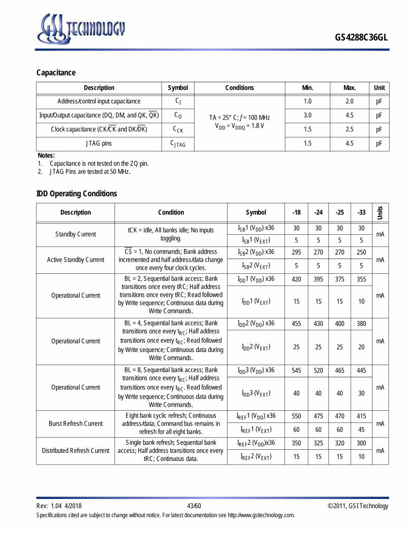
Capacitance
Description Symbol Conditions Min. Max. Unit
Address/control input capacitance CI
TA = 25° C; f = 100 MHzVDD = VDDQ = 1.8 V
1.0 2.0 pF
Input/Output capacitance (DQ, DM, and QK, QK) CO 3.0 4.5 pF
Clock capacitance (CK/CK and DK/DK) CCK 1.5 2.5 pF
JTAG pins CJTAG 1.5 4.5 pF
Notes:1. Capacitance is not tested on the ZQ pin.2. JTAG Pins are tested at 50 MHz.
IDD Operating Conditions
Description Condition Symbol -18 -24 -25 -33
Uni
ts
Standby CurrenttCK = idle, All banks idle; No inputs
toggling.
ISB1 (VDD) x36 30 30 30 30mA
ISB1 (VEXT) 5 5 5 5
Active Standby CurrentCS = 1, No commands; Bank address
incremented and half address/data change once every four clock cycles.
ISB2 (VDD) x36 295 270 270 250mA
ISB2 (VEXT) 5 5 5 5
Operational Current
BL = 2, Sequential bank access; Bank transitions once every tRC; Half address
transitions once every tRC; Read followed by Write sequence; Continuous data during
Write Commands.
IDD1 (VDD) x36 420 395 375 355
mAIDD1 (VEXT) 15 15 15 10
Operational Current
BL = 4, Sequential bank access; Bank transitions once every tRC; Half address
transitions once every tRC; Read followed by Write sequence; Continuous data during
Write Commands.
IDD2 (VDD) x36 455 430 400 380
mAIDD2 (VEXT) 25 25 25 20
Operational Current
BL = 8, Sequential bank access; Bank transitions once every tRC; Half address
transitions once every tRC. Read followed by Write sequence; Continuous data during
Write Commands.
IDD3 (VDD) x36 545 520 465 445
mAIDD3 (VEXT) 40 40 40 30
Burst Refresh CurrentEight bank cyclic refresh; Continuous
address/data; Command bus remains in refresh for all eight banks.
IREF1 (VDD) x36 550 475 470 415mA
IREF1 (VEXT) 60 60 60 45
Distributed Refresh CurrentSingle bank refresh; Sequential bank
access; Half address transitions once every tRC; Continuous data.
IREF2 (VDD)x36 350 325 320 300mA
IREF2 (VEXT) 15 15 15 10

GS4288C36GL
Specifications cited are subject to change without notice. For latest documentation see http://www.gsitechnology.com.
Rev: 1.04 4/2018 44/60 © 2011, GSI Technology
Operating Burst Write Current Example
BL= 2; Cyclic bank access; Half of address bits change every clock cycle; Continuous
data; Measurement is taken during continuous Write.
IDD2W (VDD) x36 835 715 715 620
mAIDD2W (VEXT) 60 60 60 45
Operating Burst Write Current Example
BL= 4; Cyclic bank access; Half of address bits change every two clock cycles;
Continuous data; Measurement is taken during continuous Write.
IDD4W (VDD) x36 735 630 630 545
mAIDD4W (VEXT) 55 55 55 40
Operating Burst Write Current Example
BL= 8; Cyclic bank access; Half of address bits change every four clock cycles;
Continuous data; Measurement is taken during continuous Write.
IDD8W (VDD) x36 695 595 595 515
mAIDD8W (VEXT) 55 55 55 40
Operating Burst Read Current Example
BL= 2; Cyclic bank access; Half of address bits change every clock cycle; Continuous
data; Measurement is taken during continuous Read.
IDD2R (VDD)x36 735 630 630 545
mAIDD2R (VEXT) 60 60 60 45
Operating Burst Read Current Example
BL= 4; Cyclic bank access; Half of address bits change every two clock cycles;
Continuous data; Measurement is taken during continuous Read.
IDD4R (VDD) x36 675 570 570 490
mAIDD4R (VEXT) 55 55 55 40
Operating Burst Read Current Example
BL= 8; Cyclic bank access; Half of address bits change every four clock cycles;
Continuous data; Measurement is taken during continuous Read.
IDD8R (VDD) x36 650 550 550 475
mAIDD8R (VEXT) 55 55 55 40
Notes: 1. IDD specifications are tested after the device is properly initialized and is operating at worst-case rated temperature and voltage specifications. 2. Definitions of IDD Conditions:
3a. Low is defined as VIN VIL(AC) MAX.
3b. High is defined as VIN VIH(AC) MIN.3c. Stable is defined as inputs remaining at a High or Low level.3d. Floating is defined as inputs at VREF = VDDQ/2. 3e. Continuous data is defined as half the DQ signals changng between High and Low every half clock cycle (twice per clock).3f. Continuous address is defined as half the address signals changing between High and Low every clock cycles (once per clock).3g. Sequential bank access is defined as the bank address incrementing by one every tRC.3h. Cyclic bank access is defined as the bank address incrementing by one for each command access. For BL = 2 this is every clock, for BL = 4 this
is every other clock, and for BL = 8 this is every fourth clock. 3. CS is High unless a Read, Write, AREF, or MRS command is registered. CS never transitions more than once per clock cycle. 4. IDD parameters are specified with ODT disabled.5. Tests for AC timing, IDD, and electrical AC and DC characteristics may be conducted at nominal reference/supply voltage levels, but the related
specifications and device operations are tested for the full voltage range specified.6. IDD tests may use a VIL-to-VIH swing of up to 1.5 V in the test environment, but input timing is still referenced to VREF (or to the crossing point for CK/CK), and
parameter specifications are tested for the specified AC input levels under normal use conditions. The minimum slew rate for the input signals used to test the device is 2 V/ns in the range between VIL(AC) andVIH(AC).
IDD Operating Conditions (Continued)
Description Condition Symbol -18 -24 -25 -33
Uni
ts

GS4288C36GL
Specifications cited are subject to change without notice. For latest documentation see http://www.gsitechnology.com.
Rev: 1.04 4/2018 45/60 © 2011, GSI Technology
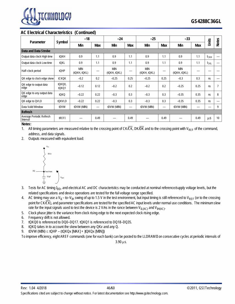
AC Electrical Characteristics
Parameter Symbol–18 –24 –25 –33
Uni
ts
Not
es
Min Max Min Max Min Max Min Max
Clock
Input Clock Cycle Time tCK 1.875 5.7 2.5 5.7 2.5 5.7 3.3 5.7 ns —
Input data clock cycle time tDK tCK tCK tCK tCK ns —
Clock jitter: period tJITPER –100 100 –150 150 –150 150 –200 200 ps 5, 6
Clock jitter: cycle-to-cycle tJITCC — 200 — 300 — 300 — 400 ps —
Clock High TimetCKHtDKH
0.45 0.55 0.45 0.55 0.45 0.55 0.45 0.55 tCK —
Clock Low TimetCKLtDKL
0.45 0.55 0.45 0.55 0.45 0.55 0.45 0.55 tCK —
Clock to input data clock tCKDK –0.3 0.3 –0.45 0.5 –0.45 0.5 –0.45 1.2 ns —
Mode register set cycle time to any command tMRSC 6 — 6 — 6 — 6 — tCK —
Setup TimesAddress/command and input setup time tAS/tCS 0.3 — 0.4 — 0.4 — 0.5 — ns —
Data–in and data mask to DK set up time tDS 0.17 — 0.25 — 0.25 — 0.3 — ns —
Hold TimesAddress/command and input hold time tAH/tCS 0.3 — 0.4 — 0.4 — 0.5 — ns —
Data-in and data mask to DK setup time tDH 0.17 — 0.25 — 0.25 — 0.3 — ns —
Notes:1. All timing parameters are measured relative to the crossing point of CK/CK, DK/DK and to the crossing point with VREF of the command,
address, and data signals. 2. Outputs measured with equivalent load:
VTT
50
Test Point
10 pF
DQ
VOUT
3. Tests for AC timing IDD, and electrical AC and DC characteristics may be conducted at nominal reference/supply voltage levels, but the related specifications and device operations are tested for the full voltage range specified.
4. AC timing may use a VIL– to–VIH swing of up to 1.5 V in the test environment, but input timing is still referenced to VREF (or to the crossing point for CK/CK), and parameter specifications are tested for the specified AC input levels under normal use conditions. The minimum slew rate for the input signals used to test the device is 2 V/ns in the rance between VIL(AC) and VIH(AC).
5. Clock phase jitter is the variance from clock rising edge to the next expected clock rising edge.6. Frequency drift is not allowed.7. tQKQ0 is referenced to DQ0–DQ17. tQKQ1 is referenced to DQ18–DQ35. 8. tQKQ takes in to account the skew between any QKx and any Q.9. tDVW (MIN) tQHP – (tQKQx [MAX] + |tQKQx [MIN]|)To improve efficiency, eight AREF commands (one for each bank) can be posted to the LLDRAM II on consecutive cycles at periodic intervals of
3.90 s
GS4288C36GL
Specifications cited are subject to change without notice. For latest documentation see http://www.gsitechnology.com.
Rev: 1.04 4/2018 46/60 © 2011, GSI Technology
Data and Data Strobe
Output data clock High time tQKH 0.9 1.1 0.9 1.1 0.9 1.1 0.9 1.1 tCKH —
Output data clock Low time tQKL 0.9 1.1 0.9 1.1 0.9 1.1 0.9 1.1 tCKL —
Half–clock period tQHPMIN
(tQKH, tQKL)—
MIN(tQKH, tQKL)
—MIN
(tQKH, tQKL)—
MIN(tQKH, tQKL)
— — —
QK edge to clock edge skew tCKQK –0.2 0.2 –0.25 0.25 –0.25 0.25 –0.3 0.3 ns —
QK edge to output data edge
tQKQ0,tQKQ1
–0.12 0.12 –0.2 0.2 –0.2 0.2 –0.25 0.25 ns 7
QK edge to any output data edge tQKQ –0.22 0.22 –0.3 0.3 –0.3 0.3 –0.35 0.35 ns 8
QK edge to QVLD tQKVLD –0.22 0.22 –0.3 0.3 –0.3 0.3 –0.35 0.35 ns —
Data Valid Window tDVW tDVW (MIN) — tDVW (MIN) — tDVW (MIN) — tDVW (MIN) — — 9
RefreshAverage Periodic RefreshInterval tREFI — 0.49 — 0.49 — 0.49 — 0.49 s 10
VTT
50
Test Point
10 pF
DQ
VOUT
AC Electrical Characteristics (Continued)
Parameter Symbol–18 –24 –25 –33
Uni
ts
Not
es
Min Max Min Max Min Max Min Max
Notes:1. All timing parameters are measured relative to the crossing point of CK/CK, DK/DK and to the crossing point with VREF of the command,
address, and data signals. 2. Outputs measured with equivalent load:
3. Tests for AC timing IDD, and electrical AC and DC characteristics may be conducted at nominal reference/supply voltage levels, but the related specifications and device operations are tested for the full voltage range specified.
4. AC timing may use a VIL– to–VIH swing of up to 1.5 V in the test environment, but input timing is still referenced to VREF (or to the crossing point for CK/CK), and parameter specifications are tested for the specified AC input levels under normal use conditions. The minimum slew rate for the input signals used to test the device is 2 V/ns in the rance between VIL(AC) and VIH(AC).
5. Clock phase jitter is the variance from clock rising edge to the next expected clock rising edge.6. Frequency drift is not allowed.7. tQKQ0 is referenced to DQ0–DQ17. tQKQ1 is referenced to DQ18–DQ35. 8. tQKQ takes in to account the skew between any QKx and any Q.9. tDVW (MIN) tQHP – (tQKQx [MAX] + |tQKQx [MIN]|)To improve efficiency, eight AREF commands (one for each bank) can be posted to the LLDRAM II on consecutive cycles at periodic intervals of
3.90 s

GS4288C36GL
Specifications cited are subject to change without notice. For latest documentation see http://www.gsitechnology.com.
Rev: 1.04 4/2018 47/60 © 2011, GSI Technology
Read Data Valid Window for x36 Device
Notes:1. tQHP is defined as the lesser of tQKH or tQKL.2. tQKQ0 is referenced to DQ0–DQ17.3. Minimum data valid window (tDVW) can be expressed as tQHP – (tQKQx [MAX] + |tQKQx [MIN]|).4. tQKQ1 is referenced to DQ18–DQ35.5. tQKQ takes into account the skew between any QKx and any DQ.
'B1 'B0
'B0 'B1
'B1 'B0
'B0 'B1
'B1 'B0
'B0 'B1
'B1 'B0
'B0 'B1
'B1 'B0
'HZZZ 'H1ZX'H1XX'H1XX'H1X5'H155 'H054'H0D6'H092'H0BA'H0AA 'HZAX'HZXX'HZXX'HZXZ'HZZZ
'B0 'B1
'B1 'B0
'B0 'B1
'B1 'B0
'B0 'B1
'B1 'B0
'B0 'B1
'B1 'B0
'B0 'B1
'HZZZ 'H0ZX'H0XX'H0XX'H0XA'H0AA 'H1AB'H129'H16D'H145'H155 'HZ5X'HZXX'HZXX'HZXZ'HZZZ
tQHP1 tQHP1tQHP1 tQHP1
tQKQ0(Min)tQKQ0(Min)
tDVW3
tQKQ0(Max)
tQKQ0(Min)
tDVW3
tQKQ0(Min)
tDVW3
tQKQ0(Max)
tQKQ0(Min)
tDVW3
tQKQ0(Min)
tQHP1 tQHP1tQHP1 tQHP1
tQKQ1(Min)
tDVW3tQKQ1(Max) tDVW3
tQKQ1(Min)
tDVW3
tQKQ0(Max)
tDVW3
tQKQ1(Min)
QK0QK0
DQ_Lower_0
DQ_Lower_1
DQ_Lower_2
DQ_Lower_3
DQ_Lower_...
DQ_Lower_14
DQ_Lower_15
DQ_Lower_16
DQ_Lower_17
DQ_Lower
QK1QK1
DQ_Upper_18
DQ_Upper_19
DQ_Upper_20
DQ_Upper_21
DQ_Upper_...
DQ_Upper_32
DQ_Upper_33
DQ_Upper_34
DQ_Upper_35
DQ_Upper

GS4288C36GL
Specifications cited are subject to change without notice. For latest documentation see http://www.gsitechnology.com.
Rev: 1.04 4/2018 48/60 © 2011, GSI Technology
Read Burst Timing
IEEE 1149.1 Serial Boundary Scan (JTAG)LLDRAM II includes an IEEE 1149.1 (JTAG) serial boundary scan Test Access Port (TAP). JTAG ports are generally used to verify the connectivity of the device once it has been mounted on a Printed Circuit Board (PCB). The port operates in accordance with IEEE Standard 1149.1-2001 (JTAG). Because the ZQ pin is actually an analog output, to ensure proper boundary-scan testing of the ZQ pin, Mode Register Bit 8 (M8) needs to be set to 0 until the JTAG testing of the pin is complete. Note that upon power up, the default state of Mode Register Bit 8 (M8) is Low.
Whenever the JTAG port is used prior to the initialization of the LLDRAM II device, such as when initial connectivity testing is conducted, it is critical that the CK and CK pins meet VID(DC) or that CS be held High from power-up until testing begins. Failure
to do so can result in inadvertent MRS commands being loaded and causing unexpected test results. Alternately a partial initialization can be conducted that consists of simply loading a single MRS command with desired MRS Register settings. JTAG testing may then begin as soon as tMRSC is satisfied. JTAG testing can be conducted after full initialization, as well.
The input signals of the test access port (TDI, TMS, and TCK) are referenced to the VDD as a supply, while the output driver of the
TAP (TDO) is powered by VDDQ.
The JTAG test access port incorporates a standard TAP controller from which the Instruction Register, Boundary Scan Register, Bypass Register, and ID Code Register can be selected. Each of these functions of the TAP controller are described below.
Disabling the JTAG FeatureUse of the JTAG port is never required for RAM operation. To disable the TAP controller, TCK must be tied Low (VSS) to prevent
clocking of the device. TDI and TMS are internally pulled up and may be unconnected or they can be connected to VDD directly or
through a pull-up resistor. TDO should be left unconnected. Upon power-up, the device will come up in a reset state, which will not interfere with the operation of the device.
Test Access Port (TAP)
Test Clock (TCK)The test clock is used only with the TAP controller. All inputs are captured on the rising edge of TCK. All outputs are driven from the falling edge of TCK.
Test Mode Select (TMS)The TMS input is used to give commands to the TAP controller and is sampled on the rising edge of TCK.
All of the states in the TAP Controller State Diagram are entered through the serial input of the TMS pin. A “0” in the diagram represents a Low on the TMS pin during the rising edge of TCK while a “1” represents a High on TMS.
Q0 Q1 Q2 Q3
tDVWtDVW
tQKQmin
tQKQmax
tQKVLDmintQKVLDmax
tQKHtQKHtQKLtQKLtCKQK
tCKtCKtCKLtCKLtCKHtCKH
CK
CK
QKx
QKx
QVLD
DQ

GS4288C36GL
Specifications cited are subject to change without notice. For latest documentation see http://www.gsitechnology.com.
Rev: 1.04 4/2018 49/60 © 2011, GSI Technology
Test Data-In (TDI)The TDI ball is used to serially input test instructions and data into the registers and can be connected to the input of any of the registers. The register between TDI and TDO is chosen by the instruction that is loaded into the TAP instruction register. For information on loading the instruction register, see the TAP Controller State Diagram. TDI is connected to the Most Significant Bit (MSB) of any register (see the TAP Controller Block Diagram).
Test Data-Out (TDO)The TDO output ball is used to serially clock test instructions and data out from the registers. The TDO output driver is only active during the Shift-IR and Shift-DR TAP controller states. In all other states, the TDO pin is in a High-Z state. The output changes on the falling edge of TCK. TDO is connected to the Least Significant Bit (LSB) of any register (see the TAP Controller Block Diagram).
TAP ControllerThe TAP controller is a finite state machine that uses the state of the TMS pin at the rising edge of TCK to navigate through its various modes of operation. See the TAP Controller State Diagram. Each state is described in detail below.
Test-Logic-ResetThe test-logic-reset controller state is entered when TMS is held High for at least five consecutive rising edges of TCK. As long as TMS remains High, the TAP controller will remain in the test-logic-reset state. The test logic is inactive during this state.
Run-Test/IdleThe run-test/idle is a controller state in between scan operations. This state can be maintained by holding TMS Low. From here either the data register scan, or subsequently, the instruction register scan can be selected.
Select-DR-ScanSelect-DR-scan is a temporary controller state. All test data registers retain their previous state while here.
Capture-DRThe Capture-DR state is where the data is parallel-loaded into the test data registers. If the Boundary Scan Register is the currently selected register, then the data currently on the pins is latched into the test data registers.
Shift-DRData is shifted serially through the data register while in this state. As new data is input through the TDI pin, data is shifted out of the TDO pin.
Exit1-DR, Pause-DR, and Exit2-DRThe purpose of Exit1-DR is used to provide a path to return back to the run-test/idle state (through the Update-DR state). The Pause-DR state is entered when the shifting of data through the test registers needs to be suspended. When shifting is to reconvene, the controller enters the Exit2-DR state and then can re-enter the Shift-DR state.
Update-DRWhen the EXTEST instruction is selected, there are latched parallel outputs of the boundary scan shift register that only change state during the Update-DR controller state.
Instruction Register StatesThe instruction register states of the TAP controller are similar to the data register states. The desired instruction is serially shifted into the instruction register during the Shift-IR state and is loaded during the Update-IR state.
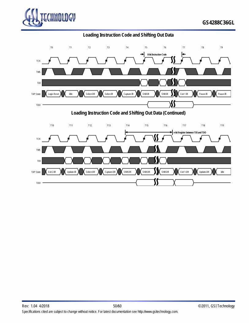
GS4288C36GL
Specifications cited are subject to change without notice. For latest documentation see http://www.gsitechnology.com.
Rev: 1.04 4/2018 50/60 © 2011, GSI Technology
Loading Instruction Code and Shifting Out Data
Loading Instruction Code and Shifting Out Data (Continued)
T0 T1 T2 T3 T4 T5 T6 T7 T8 T9
Logic-Reset Idle Select-DR Select-IR Capture-IR Shift-IR Shift-IR Exit 1-IR Pause-IR Pause-IR
8-bit Instruction Code8-bit Instruction Code
TCK
TMS
TDI
TAP State
TDO
T10 T11 T12 T13 T14 T15 T16 T17 T18 T19
Exit 2-IR Update-IR Select-DR Capture-DR Shift-DR Shift-DR Shift-DR Exit 1-DR Update-DR Idle
n-bit Register between TDI and TDOn-bit Register between TDI and TDO
TCK
TMS
TDI
TAP State
TDO

GS4288C36GL
Specifications cited are subject to change without notice. For latest documentation see http://www.gsitechnology.com.
Rev: 1.04 4/2018 51/60 © 2011, GSI Technology
JTAG Tap Controller State Diagram
Select DR-scan
Capture-DR
Shift-DR
Exit1-DR
Pause-DR
Exit2-DR
Update-DR
Select IR-scan
Capture-IR
Shift-IR
Exit1-IR
Pause-IR
Exit2-IR
Update-IR
Test Logic Reset
Run Test Idle0
0
1
0
1
1
0
0
1
1
1
0
0
1
0
0 0
0
1
1
0 0
1 1 00
0
1
1 1 1
1
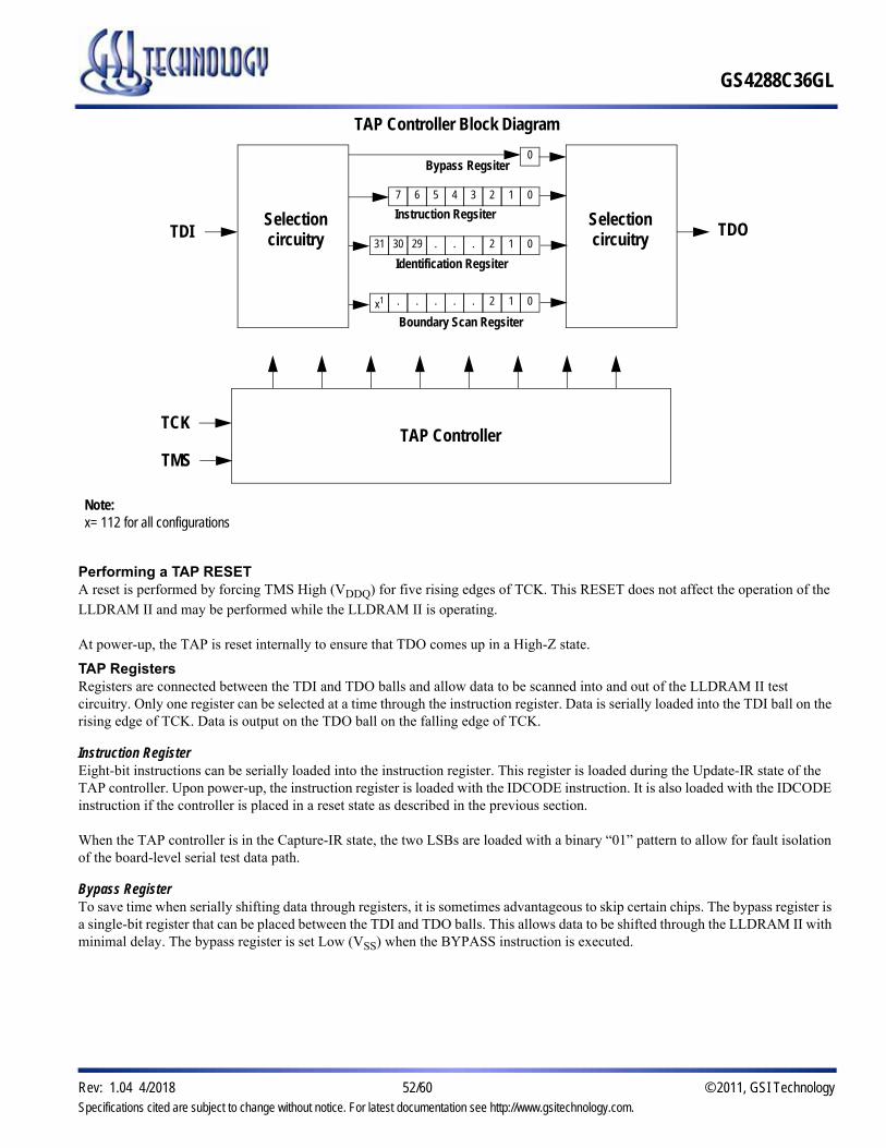
GS4288C36GL
Specifications cited are subject to change without notice. For latest documentation see http://www.gsitechnology.com.
Rev: 1.04 4/2018 52/60 © 2011, GSI Technology
TAP Controller Block Diagram
Performing a TAP RESETA reset is performed by forcing TMS High (VDDQ) for five rising edges of TCK. This RESET does not affect the operation of the
LLDRAM II and may be performed while the LLDRAM II is operating.
At power-up, the TAP is reset internally to ensure that TDO comes up in a High-Z state.
TAP RegistersRegisters are connected between the TDI and TDO balls and allow data to be scanned into and out of the LLDRAM II test circuitry. Only one register can be selected at a time through the instruction register. Data is serially loaded into the TDI ball on the rising edge of TCK. Data is output on the TDO ball on the falling edge of TCK.
Instruction RegisterEight-bit instructions can be serially loaded into the instruction register. This register is loaded during the Update-IR state of the TAP controller. Upon power-up, the instruction register is loaded with the IDCODE instruction. It is also loaded with the IDCODE instruction if the controller is placed in a reset state as described in the previous section.
When the TAP controller is in the Capture-IR state, the two LSBs are loaded with a binary “01” pattern to allow for fault isolation of the board-level serial test data path.
Bypass RegisterTo save time when serially shifting data through registers, it is sometimes advantageous to skip certain chips. The bypass register is a single-bit register that can be placed between the TDI and TDO balls. This allows data to be shifted through the LLDRAM II with minimal delay. The bypass register is set Low (VSS) when the BYPASS instruction is executed.
x1 . . . . . 2 1 0
31 30 29 . . . 2 1 0
0
7 6 5 4 3 2 1 0
Selectioncircuitry
Selectioncircuitry TDOTDI
Bypass Regsiter
Instruction Regsiter
Identification Regsiter
Boundary Scan Regsiter
TCK
TMSTAP Controller
Note: x= 112 for all configurations

GS4288C36GL
Specifications cited are subject to change without notice. For latest documentation see http://www.gsitechnology.com.
Rev: 1.04 4/2018 53/60 © 2011, GSI Technology
Boundary Scan RegisterThe Boundary Scan Register is connected to all the input and bidirectional balls on the LLDRAM II. Several bits are also included in the scan register for reserved balls. The LLDRAM II has a 113-bit register.
The Boundary Scan Register is loaded with the contents of the RAM I/O ring when the TAP controller is in the Capture-DR state and is then placed between the TDI and TDO balls when the controller is moved to the Shift-DR state.
The Boundary Scan Register table shows the order in which the bits are connected. Each bit corresponds to one of the balls on the LLDRAM II package. The MSB of the register is connected to TDI, and the LSB is connected to TDO.
Identification (ID) RegisterThe ID register is loaded with a vendor-specific, 32-bit code during the capture-DR state when the IDCODE command is loaded in the instruction register. The IDCODE is hardwired into the LLDRAM II and can be shifted out when the TAP controller is in the shift-DR state. The ID register has a vendor code and other information described in the table below.
TAP Instruction Set
OverviewMany different instructions (256) are possible with the 8-bit instruction register. All combinations used are listed in the Instruction Codes table. These six instructions are described in detail below. The remaining instructions are reserved and should not be used.
The TAP controller used in this LLDRAM II is fully compliant to the 1149.1 convention.
Instructions are loaded into the TAP controller during the Shift-IR state when the instruction register is placed between TDI and TDO. During this state, instructions are shifted through the instruction register through the TDI and TDO balls. To execute the instruction once it is shifted in, the TAP controller needs to be moved into the Update-IR state.
EXTESTThe EXTEST instruction allows circuitry external to the component package to be tested. Boundary Scan Register cells at output balls are used to apply a test vector, while those at input balls capture test results. Typically, the first test vector to be applied using the EXTEST instruction will be shifted into the Boundary Scan Register using the PRELOAD instruction. Thus, during the Update-IR state of EXTEST, the output driver is turned on, and the PRELOAD data is driven onto the output balls.
IDCODEThe IDCODE instruction causes a vendor-specific, 32-bit code to be loaded into the instruction register. It also places the instruction register between the TDI and TDO balls and allows the IDCODE to be shifted out of the device when the TAP controller enters the Shift-DR state. The IDCODE instruction is loaded into the instruction register upon power-up or whenever the TAP controller is given a test logic reset state.
Identification Register Definitions
Instruction Field Bit Size Bit Size
Revision number (31:28) abcdab = die revisioncd = 10 for x36
Device ID (27:12) 00jkidef10100111def = 000 for 288Mb
i = 0 for common I/O, 1 for separate I/Ojk = 01 for LLDRAM II
GSI JEDEC ID code (11:1) 01011011001 Allows unique identification of LLDRAM II vendor
ID register presence indicator (0) 1 Indicates the presence of an ID register

GS4288C36GL
Specifications cited are subject to change without notice. For latest documentation see http://www.gsitechnology.com.
Rev: 1.04 4/2018 54/60 © 2011, GSI Technology
High-ZThe High-Z instruction places all LLDRAM II outputs into a High-Z state, and causes the bypass register to be connected between TDI and TDO when the TAP Controller is in the Shift DR state.
CLAMPWhen the CLAMP instruction is loaded into the instruction register, the data driven by the output balls are determined from the values held in the Boundary Scan Register. Additionally, it causes the bypass register to be connected between TDI and TDO when the TAP Controller is in the Shift DR state.
SAMPLE/PRELOADWhen the SAMPLE/PRELOAD instruction is loaded into the instruction register and the TAP controller is in the Capture-DR state, a snapshot of data on the inputs and bidirectional balls is captured in the Boundary Scan Register.
The user must be aware that the TAP controller clock can only operate at a frequency up to 50 MHz, while the LLDRAM II clock operates significantly faster. Because there is a large difference between the clock frequencies, it is possible that during the Capture-DR state, an input or output will undergo a transition. The TAP may then try to capture a signal while in transition (metastable state). This will not harm the device, but there is no guarantee as to the value that will be captured. Repeatable results may not be possible.
To ensure that the Boundary Scan Register will capture the correct value of a signal, the LLDRAM II signal must be stabilized long enough to meet the TAP controller’s capture setup plus hold time (tCS + tCH). The LLDRAM II clock input might not be captured correctly if there is no way in a design to stop (or slow) the clock during a SAMPLE/PRELOAD instruction. If this is an issue, it is still possible to capture all other signals and simply ignore the value of the CK and CK captured in the Boundary Scan Register.
Once the data is captured, it is possible to shift out the data by putting the TAP into the Shift-DR state. This places the Boundary Scan Register between the TDI and TDO balls.
BYPASSWhen the BYPASS instruction is loaded in the instruction register and the TAP is placed in a Shift-DR state, the bypass register is placed between TDI and TDO. The advantage of the BYPASS instruction is that it shortens the boundary scan path when multiple devices are connected together on a board.
Reserved for Future UseThe remaining instructions are not implemented but are reserved for future use. Do not use these instructions.
TAP Timing
T0 T1 T2 T3 T4 T5
tTLOV
tTLOX
tTHDX
tDVTH
tTHMX
tMVTH
tTHTHtTHTH
tTLTHtTLTH
tTHTLtTHTL
Test Clock (TCK)
Test Mode Select (TMS)
Test Data-In (TDI)
Test Data-Out (TDO)
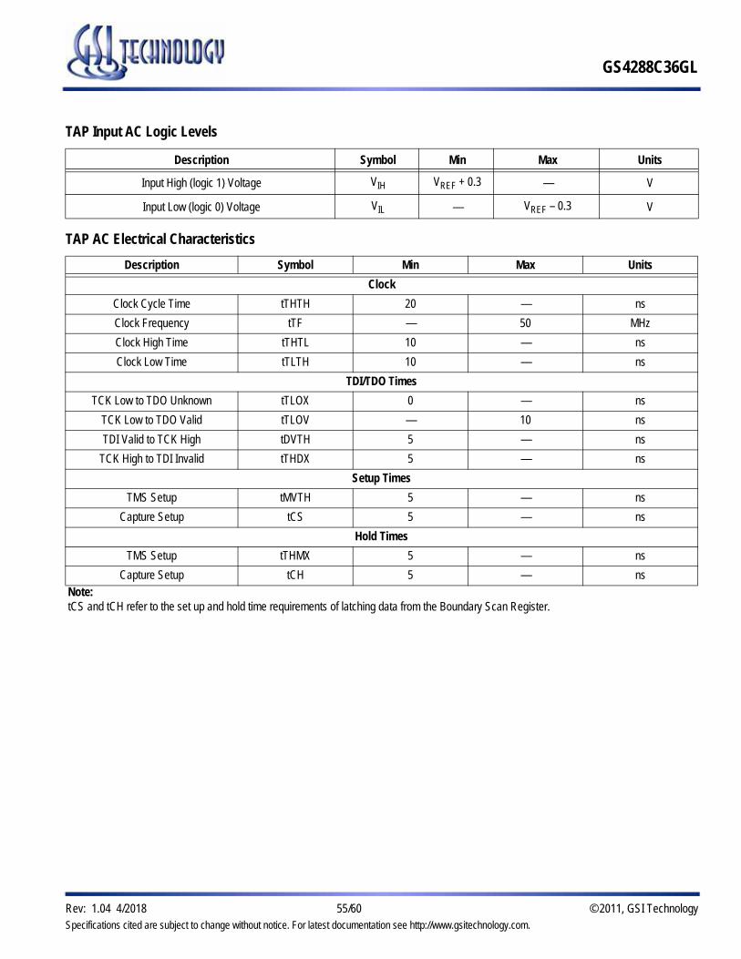
GS4288C36GL
Specifications cited are subject to change without notice. For latest documentation see http://www.gsitechnology.com.
Rev: 1.04 4/2018 55/60 © 2011, GSI Technology
TAP Input AC Logic Levels
Description Symbol Min Max Units
Input High (logic 1) Voltage VIH VREF + 0.3 — V
Input Low (logic 0) Voltage VIL — VREF – 0.3 V
TAP AC Electrical Characteristics
Description Symbol Min Max Units
Clock
Clock Cycle Time tTHTH 20 — ns
Clock Frequency tTF — 50 MHz
Clock High Time tTHTL 10 — ns
Clock Low Time tTLTH 10 — ns
TDI/TDO Times
TCK Low to TDO Unknown tTLOX 0 — ns
TCK Low to TDO Valid tTLOV — 10 ns
TDI Valid to TCK High tDVTH 5 — ns
TCK High to TDI Invalid tTHDX 5 — ns
Setup Times
TMS Setup tMVTH 5 — ns
Capture Setup tCS 5 — ns
Hold Times
TMS Setup tTHMX 5 — ns
Capture Setup tCH 5 — nsNote:tCS and tCH refer to the set up and hold time requirements of latching data from the Boundary Scan Register.

GS4288C36GL
Specifications cited are subject to change without notice. For latest documentation see http://www.gsitechnology.com.
Rev: 1.04 4/2018 56/60 © 2011, GSI Technology
TAP DC Electrical Characteristics and Operating Conditions
Description Condition Symbol Min Max Units Notes
Input High (logic 1) Voltage — VIH VREF + 0.15 VDD + 0.3 V 1, 2
Input High (logic 0) Voltage — VIL VSS – 0.3 VREF – 0.15 V 1, 2
Input Leakage CurrentOutput disabled,0 VVIN VDDQ
ILI –5.0 5.0 —
Output Leakage Current 0 VVIN VDD ILO –5.0 5.0 —
Output Low Voltage IOLC = 100 VOL1 — 0.2 V 1
Output Low Voltage IOLT = 2mA VOL2 — 0.4 V 1
Output High Voltage IOHC = 100 VOH1 VDDQ – 0.2 — V 1
Output High Voltage IOHT= 2mA VOH2 VDDQ – 0.4 — V 1
Notes:1. All voltages referenced to VSS (GND).
2. Overshoot = VIH(AC) VDD + 0.7 V for t tTHTH/2; undershoot = VIL(AC)– 0.5 V for t tTHTH/2; during normal operation, VDDQ must not exceed VDD.
Scan Register Sizes
Register Name Bit Size
Instruction 8
Bypass 1
ID 32
Boundary Scan 113
JTAG TAP Instruction Codes
Instruction Code Description
EXTEST 0000 0000 Captures I/O ring contents; Places the Boundary Scan Register between TDI and TDO. Data driven by output balls are determined from values held in the Boundary Scan Register.
IDCODE 0010 0001Loads the ID register with the vendor ID code and places the register between TDI and TDO. This operation does not affect LLDRAM II operations.
SAMPLE/PRELOAD 0000 0101Captures I/O ring contents. Places the Boundary Scan Register between TDI and TDO. This operation does not affect LLDRAM II operations.
CLAMP 0000 0111Selects the bypass register to be connected between TDI and TDO. Data driven by output balls are determined from values held in the Boundary Scan Register.
HIGH-Z 0000 0011Selects the bypass register to be connected between TDI and TDO. All outputs are forced into High-Z.
BYPASS 1111 1111Places Bypass Register between TDI and TDO.This operation does not affect LLDRAM II operations.

GS4288C36GL
Specifications cited are subject to change without notice. For latest documentation see http://www.gsitechnology.com.
Rev: 1.04 4/2018 57/60 © 2011, GSI Technology
Boundary Scan (BSDL Files)For information regarding the Boundary Scan Chain, or to obtain BSDL files for this part, please contact our Applications Engineering Department at: [email protected].
Boundary Scan Exit Order Bit # Ball Bit # Ball Bit # Ball
1 K1 39 R11 77 C112 K2 40 R11 78 C113 L2 41 P11 79 C104 L1 42 P11 80 C105 M1 43 P10 81 B116 M3 44 P10 82 B117 M2 45 N11 83 B108 N1 46 N11 84 B109 P1 47 N10 85 B3
10 N3 48 N10 86 B311 N3 49 P12 87 B212 N2 50 N12 88 B213 N2 51 M11 89 C314 P3 52 M10 90 C315 P3 53 M12 91 C216 P2 54 L12 92 C217 P2 55 L11 93 D318 R2 56 K11 94 D319 R3 57 K12 95 D220 T2 58 J12 96 D221 T2 59 J11 97 E222 T3 60 H11 98 E223 T3 61 H12 99 E324 U2 62 G12 100 E325 U2 63 G10 101 F226 U3 64 G11 102 F227 U3 65 E12 103 F328 V2 66 F12 104 F329 U10 67 F10 105 E130 U10 68 F10 106 F131 U11 69 F11 107 G232 U11 70 F11 108 G333 T10 71 E10 109 G134 T10 72 E10 110 H135 T11 73 E11 111 H236 T11 74 E11 112 J237 R10 75 D11 113 J138 R10 76 D10 — —

GS4288C36GL
Specifications cited are subject to change without notice. For latest documentation see http://www.gsitechnology.com.
Rev: 1.04 4/2018 58/60 © 2011, GSI Technology
Package Dimensions—144-Bump BGA (Package L)
A
B
C
D
E
F
G
H
J
K
L
M
N
P
R
T
U
V
1 2 3 4 5 6 7 8 9 10 11 12
12 11 10 9 8 7 6 5 4 3 2 1
A1
A1
0.80 TYP.
11.00±0.10
17.0
0 C
TR
Ø0.51 (144x)
ASEATING PLANE
1.20 MAX
0.012 A
10° TYP.
10.60 CTR.
A
B
C
D
E
F
G
H
J
K
L
M
N
P
R
T
U
V
1.0
TY
P.
8.80
18.50±0.100.73±0.1
Note: All dimensions in millimeters.
8.8 CTR
0.8 TYP0.34 MIN
18.1 CTR
0.49±0.05
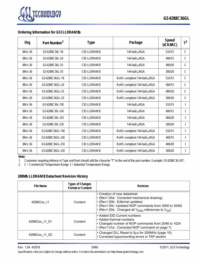
GS4288C36GL
Specifications cited are subject to change without notice. For latest documentation see http://www.gsitechnology.com.
Rev: 1.04 4/2018 59/60 © 2011, GSI Technology
Ordering Information for GSI LLDRAM IIs
Org Part Number1 Type PackageSpeed
(tCK/tRC) T2
8M x 36 GS4288C36L-18 CIO LLDRAM II 144-ball BGA 533/15 C
8M x 36 GS4288C36L-24 CIO LLDRAM II 144-ball BGA 400/15 C
8M x 36 GS4288C36L-25 CIO LLDRAM II 144-ball BGA 400/20 C
8M x 36 GS4288C36L-33 CIO LLDRAM II 144-ball BGA 300/20 C
8M x 36 GS4288C36GL-18 CIO LLDRAM II RoHS-compliant 144-ball BGA 533/15 C
8M x 36 GS4288C36GL-24 CIO LLDRAM II RoHS-compliant 144-ball BGA 400/15 C
8M x 36 GS4288C36GL-25 CIO LLDRAM II RoHS-compliant 144-ball BGA 400/20 C
8M x 36 GS4288C36GL-33 CIO LLDRAM II RoHS-compliant 144-ball BGA 300/20 C
8M x 36 GS4288C36L-18I CIO LLDRAM II 144-ball BGA 533/15 I
8M x 36 GS4288C36L-24I CIO LLDRAM II 144-ball BGA 400/15 I
8M x 36 GS4288C36L-25I CIO LLDRAM II 144-ball BGA 400/20 I
8M x 36 GS4288C36L-33I CIO LLDRAM II 144-ball BGA 300/20 I
8M x 36 GS4288C36GL-18I CIO LLDRAM II RoHS-compliant 144-ball BGA 533/15 I
8M x 36 GS4288C36GL-24I CIO LLDRAM II RoHS-compliant 144-ball BGA 400/15 I
8M x 36 GS4288C36GL-25I CIO LLDRAM II RoHS-compliant 144-ball BGA 400/20 I
8M x 36 GS4288C36GL-33I CIO LLDRAM II RoHS-compliant 144-ball BGA 300/20 I
Note:1. Customers requiring delivery in Tape and Reel should add the character “T” to the end of the part number. Example: GS4288C36-33T.2. C = Commercial Temperature Range. I = Industrial Temperature Range.
288Mb LLDRAM II Datasheet Revision History
File NameTypes of ChangesFormat or Content
Revision
4288Cxx_r1 Content
• Creation of new datasheet• (Rev1.00a: Corrected mechanical drawing)• (Rev1.00b: Editorial updates)• (Rev1.00c: Updated NOP commands from 3000 to 2048)• (Rev1.00d: Changed all VSSQ references to VSS)
4288Cxx_r1_01 Content
• Added IDD Current numbers• Added thermal numbers• Changed number of NOP commands from 2048 to 1024• (Rev1.01a: Corrected NOP command on page 7)
4288Cxx_r1_02 Content• Changed DLL Reset to 5s for 200MHz (page 10)• Corrected typos/wording errors in TAP section

GS4288C36GL
Specifications cited are subject to change without notice. For latest documentation see http://www.gsitechnology.com.
Rev: 1.04 4/2018 60/60 © 2011, GSI Technology
4288Cxx_r1_03 Content • Updated datasheet to reflect MP status
4288Cxx_r1_04 Content • Removed all references to x9 and x18 to reflect EOL status
288Mb LLDRAM II Datasheet Revision History
File NameTypes of ChangesFormat or Content
Revision

Mouser Electronics
Authorized Distributor
Click to View Pricing, Inventory, Delivery & Lifecycle Information: GSI Technology:
GS4288C36GL-25I GS4288C36GL-24I GS4288C36GL-18 GS4288C36GL-25 GS4288C36GL-33 GS4288C36GL-
18I GS4288C36GL-33I GS4288C36GL-24