ben garland, jim xu, ph.d., and vamsi velidandla zeta · pdf filezeta instruments, inc. . zeta...
TRANSCRIPT
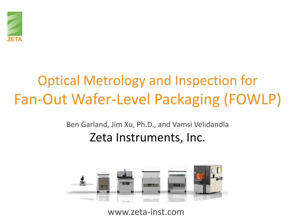
Optical Metrology and Inspection for
Fan-Out Wafer-Level Packaging (FOWLP)
Ben Garland, Jim Xu, Ph.D., and Vamsi Velidandla
Zeta Instruments, Inc.
www.zeta-inst.com

Zeta Instruments / Jun 2016 / FOWLP
• About Zeta Instruments
• FOWLP advantages and metrology challenges
• WLCSP process flow and the need for multi-mode metrology systems
– Introduction of Zeta metrology solutions
– Application examples & results
• FOWLP carrier glass defect inspection
• Summary
www.zeta-inst.com 2
Agenda

• Multi-mode optical profilers and defect inspection systems for cost effective production monitoring
• Offices in San Jose (HQ) and Shanghai
• Founded in 2009. More than 230 systems installed in 22 countries since 2010
• Focus on advanced semiconductor packaging, HBLED, glass, and solar industries
• World’s leading OSATs have adopted the Zeta WLCSP metrology solutions
• www.zeta-inst.com
www.zeta-inst.com 3
About Zeta Instruments
Zeta Instruments / Jun 2016 / FOWLP

www.zeta-inst.com 4
Multi-Mode Optics for Inspection & Metrology• Unique capabilities for difficult surfaces
Zeta3D™ Optical Profiler
Transparent and multi-layerLow reflectivity and low-contrast
High roughnessLarge height variations
High aspect ratio trenches
ZetaScan™ Defect Inspection
Transparent and thin materialsHigh roughness surfaces
Stacked substrates (glass on carrier)
Zeta Instruments Confidential / March 2016

• Advantages– Thinner package
– Higher I/O
– Improved thermal and electrical performance
• Metrology challenges– Wafer warpage
– Smaller RDL critical dimensions
– Low reflectivity and high roughness of epoxy mold compound (EMC)
www.zeta-inst.com 5
FOWLP advantages and metrology challenges
Zeta Instruments / Jun 2016 / FOWLP
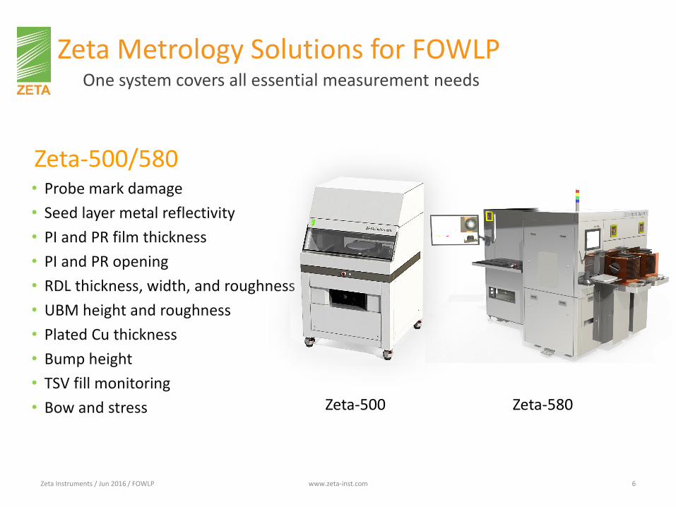
Zeta Metrology Solutions for FOWLP• One system covers all essential measurement needs
Zeta Instruments / Jun 2016 / FOWLP www.zeta-inst.com 6
Zeta-500/580• Probe mark damage
• Seed layer metal reflectivity
• PI and PR film thickness
• PI and PR opening
• RDL thickness, width, and roughness
• UBM height and roughness
• Plated Cu thickness
• Bump height
• TSV fill monitoring
• Bow and stress Zeta-500 Zeta-580

LITHOGRAPHY PROCESS MONITORING
Application examples
www.zeta-inst.com 7Zeta Instruments / Jun 2016 / FOWLP

www.zeta-inst.com 8
PI or PR thickness measurement• Full wafer mapping and statistics
Zeta Instruments / Jun 2016 / FOWLP

www.zeta-inst.com 9
Photoresist opening measurements• Automated feature detection and measurement
56
.34
µm
63.48 µm
Vias in the PR layers are automatically detected and centered within the field of view. The Zeta3D software automatically measures the via diameter as well as the depth.
Zeta Instruments / Jun 2016 / FOWLP
PLATING PROCESS MONITORING
Application examples
www.zeta-inst.com 10Zeta Instruments / Jun 2016 / FOWLP
www.zeta-inst.com 11
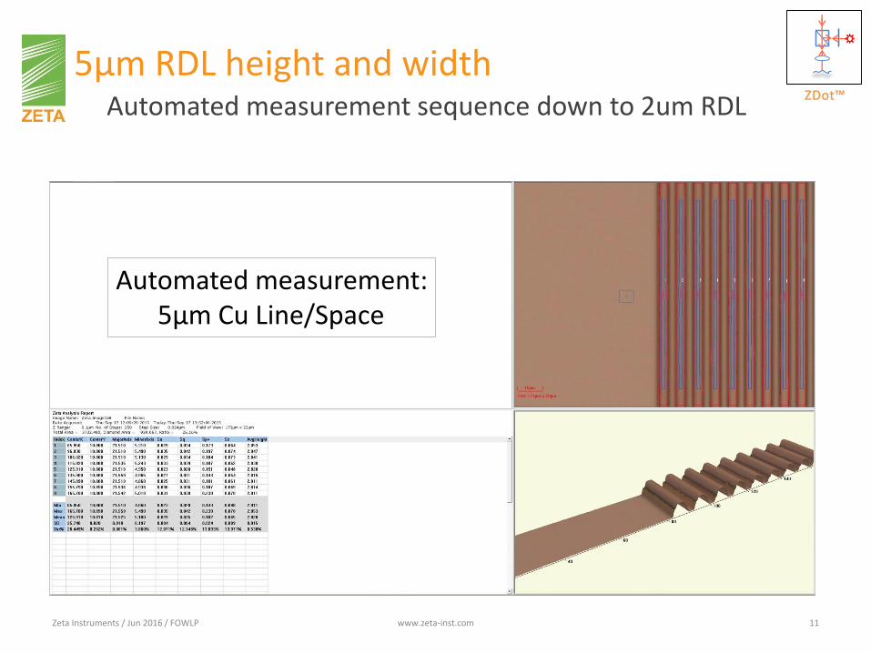
5µm RDL height and width• Automated measurement sequence down to 2um RDL
Automated measurement:5µm Cu Line/Space
Zeta Instruments / Jun 2016 / FOWLP
www.zeta-inst.com 12
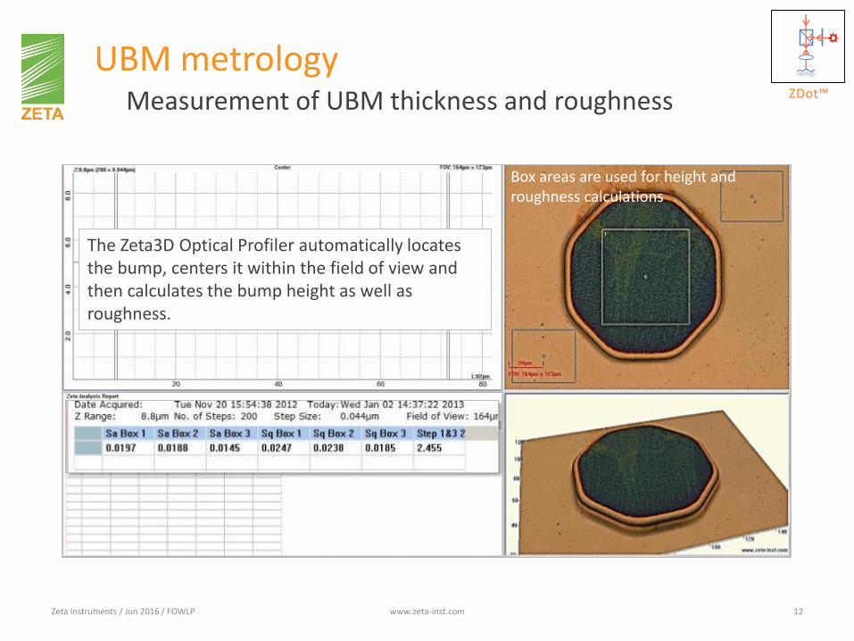
UBM metrology• Measurement of UBM thickness and roughness
Box areas are used for height and roughness calculations
The Zeta3D Optical Profiler automatically locates the bump, centers it within the field of view and then calculates the bump height as well as roughness.
Zeta Instruments / Jun 2016 / FOWLP
www.zeta-inst.com 13
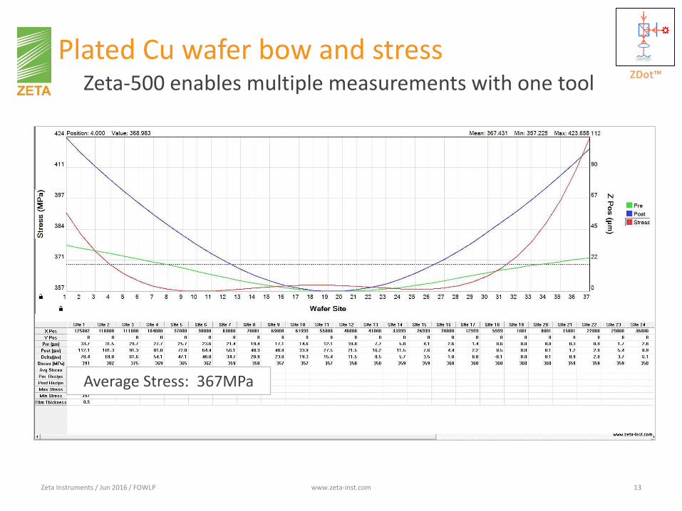
Plated Cu wafer bow and stress• Zeta-500 enables multiple measurements with one tool
Average Stress: 367MPa
Zeta Instruments / Jun 2016 / FOWLP

REFLOWED BUMP HEIGHT MONITORING
Application examples
www.zeta-inst.com 14Zeta Instruments / Jun 2016 / FOWLP
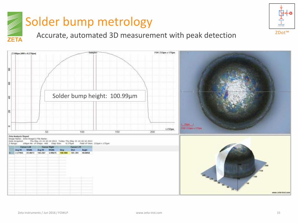
Solder bump metrology• Accurate, automated 3D measurement with peak detection
Zeta Instruments / Jun 2016 / FOWLP www.zeta-inst.com 15
Solder bump height: 100.99µm
5
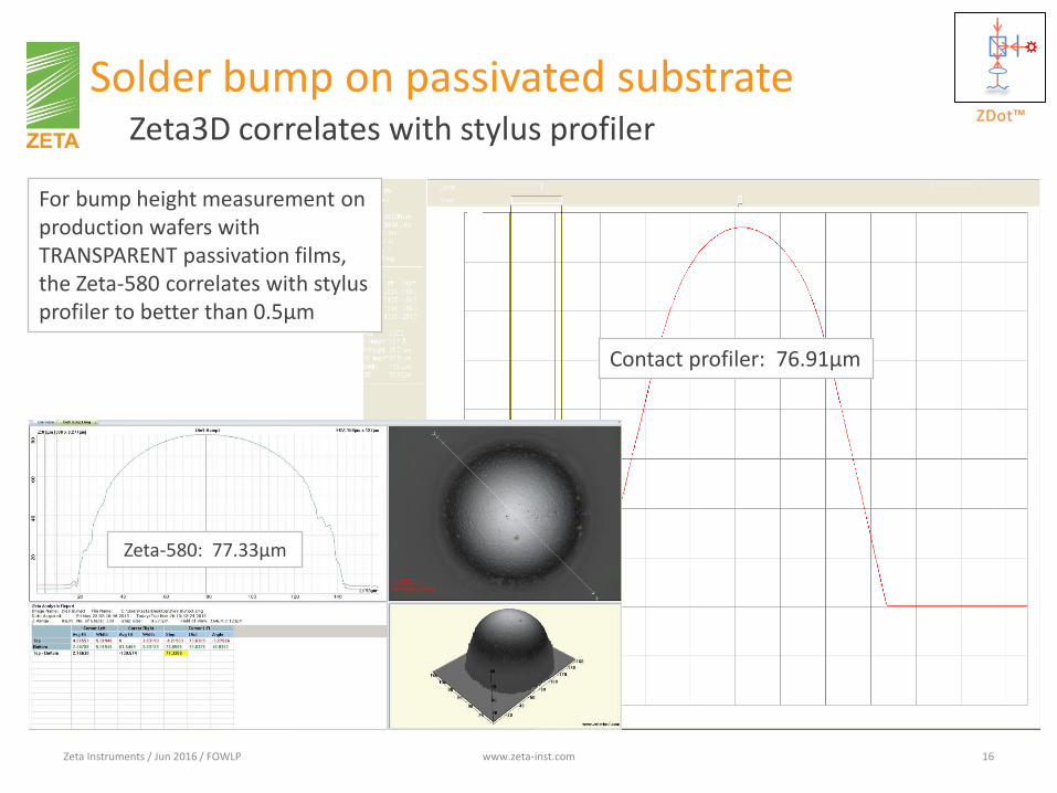
Zeta-580: 77.33µm
Contact profiler: 76.91µm
Solder bump on passivated substrate• Zeta3D correlates with stylus profiler
Zeta Instruments / Jun 2016 / FOWLP www.zeta-inst.com 16
For bump height measurement on production wafers with TRANSPARENT passivation films, the Zeta-580 correlates with stylus profiler to better than 0.5µm

LASER SCRIBE MONITORING
Application examples
www.zeta-inst.com 17Zeta Instruments / Jun 2016 / FOWLP

Laser scribe of silicon wafer• Zeta3D ideally capable for trench measurements
Zeta Instruments / Jun 2016 / FOWLP www.zeta-inst.com 18
Scribe Depth: 35.35µm

FOWLP CARRIER GLASS INSPECTION
Application examples
www.zeta-inst.com 19Zeta Instruments / Jun 2016 / FOWLP

www.zeta-inst.com 20
ZetaScan• Multi-Mode optics for inspecting transparent substrates
• Multi-Mode Optics– High throughput and high
sensitivity at low COO– Accurate defect classification– Separation of topside, backside
and interface defects
• Difficult Surfaces– Transparent and thin– High roughness– Stacked substrates– Irregular shapes and sizes
ZetaScanTM Defect Inspection
Zeta Instruments Confidential / April 2016

Multi-Mode optics enable defect classification• Advanced algorithms compare defect signatures
Notes• This table is Illustrative only• Other factors are used as necessary (defect size, double image, aspect ratio, intensities, etc.) • Recipes are developed for accurate defect classification on customer specific samples
Zeta Instruments / Jun 2016 / FOWLP www.zeta-inst.com 21
Defect Type ZSS ZTS ZSP ZTP
Top particle very bright bright dark
Bottom particle bright
Top Pit bright darkdark and bright(down-up profile)
Interface particle brightbright and dark(up-down profile)
Interface bubble bright brightbright and dark(up-down profile)
Stain dark

Carrier glass defect types• Different signatures in different channels enable detection and classification
Zeta Instruments / Jun 2016 / FOWLP www.zeta-inst.com 22
Defect Top Scatter Side Scatter Specular Topography Unique Characteristic
PitTop Scatter >> Side Scatter
Scratch High Aspect Ratio
ParticleSide Scatter > Top Scatter

Defect analysis report• Includes defect map, report and pareto chart with binning
Zeta Instruments / Jun 2016 / FOWLP www.zeta-inst.com 23
Stain Scratch Pit Particle
(µm²) (µm²) (µm²) (µm²) PSL eq (µm)
Bin 1 0-5,000 0-5,000 0-5,000 0-5,000 0.3 - 0.5
Bin 2 5,000-10,000 5,000-10,000 5,000-10,000 5,000-10,000 0.5 - 1
Bin 3 10,000-20,000 10,000-20,000 10,000-20,000 10,000-20,000 1 -2
Bin 4 20,000-30,000 20,000-30,000 20,000-30,000 20,000-30,000 2-5
Bin 5 >30,000 >30,000 >30,000 >30,000 >5
Bump

Summary
• FOWLP creates new challenges for metrology and inspection
• Automated multi-mode metrology and inspection systems provide a solution
– Better process control
– Cost effective
– User friendly
Zeta Instruments / Jun 2016 / FOWLP www.zeta-inst.com 24

Thank you!www.zeta-inst.com