beaglebone rev a3 system reference...
TRANSCRIPT

REF: BBONE_SRM BeagleBone System Reference Manual
RevA3_1.0
Page 1 of 76
BeagleBone Rev A3
System Reference Manual
Revision 1.0 December 19, 2011
Send all comments and errors to the author:
Gerald Coley [email protected]

REF: BBONE_SRM BeagleBone System Reference Manual
RevA3_1.0
Page 2 of 76
NOTE: This equipment has been tested and found to comply with the limits for a Class B digital device, pursuant to Part 15 of the FCC Rules. These limits are designed to provide reasonable protection against harmful interference when the equipment is operated in a commercial environment. This equipment generates, uses, and can radiate radio frequency energy and, if not installed and used in accordance with the instruction manual, may cause harmful interference to radio communications. Operation of this equipment in a residential area is likely to cause harmful interference in which case the user will be required to correct the interference at their own expense. All accessories used with this board must meet FCC certification to maintain compliance of this equipment.
NOTE:. If this equipment does cause harmful interference to radio or television reception, which can be determined by turning the equipment off and on, the user is encouraged to try to correct the interference by one or more of the following measures:
—Reorient or relocate the receiving antenna.
—Increase the separation between the equipment and receiver.
—Connect the equipment into an outlet on a circuit different from that to which the receiver is connected.
—Consult the dealer or an experienced radio/TV technician for help.
Changes or modifications not expressly approved by this manual for compliance could void the user’s authority to operate the equipment.
THIS DOCUMENT This work is licensed under the Creative Commons Attribution-Share Alike 3.0 Unported License. To view a copy of this license, visit http://creativecommons.org/licenses/by-sa/3.0/ or send a letter to Creative Commons, 171 Second Street, Suite 300, San Francisco, California, 94105, USA. All derivative works are to be attributed to Gerald Coley of BeagleBoard.org. For more information, see http://creativecommons.org/license/results-one?license_code=by-sa For any questions, concerns, or issues submit them to [email protected]

REF: BBONE_SRM BeagleBone System Reference Manual
RevA3_1.0
Page 3 of 76
BEAGLEBONE DESIGN These design materials referred to in this document are *NOT SUPPORTED* and DO NOT constitute a reference design. Only “community” support is allowed via resources at BeagleBoard.org/discuss. THERE IS NO WARRANTY FOR THE DESIGN MATERIALS, TO THE EXTENT PERMITTED BY APPLICABLE LAW. EXCEPT WHEN OTHERWISE STATED IN WRITING THE COPYRIGHT HOLDERS AND/OR OTHER PARTIES PROVIDE THE DESIGN MATERIALS “AS IS” WITHOUT WARRANTY OF ANY KIND, EITHER EXPRESSED OR IMPLIED, INCLUDING, BUT NOT LIMITED TO, THE IMPLIED WARRANTIES OF MERCHANTABILITY AND FITNESS FOR A PARTICULAR PURPOSE. THE ENTIRE RISK AS TO THE QUALITY AND PERFORMANCE OF THE DESIGN MATERIALS IS WITH YOU. SHOULD THE DESIGN MATERIALS PROVE DEFECTIVE, YOU ASSUME THE COST OF ALL NECESSARY SERVICING, REPAIR OR CORRECTION. We mean it; these design materials may be totally unsuitable for any purposes.

REF: BBONE_SRM BeagleBone System Reference Manual
RevA3_1.0
Page 4 of 76
BeagleBoard.org provides the enclosed product(s) under the following conditions: This evaluation board/kit is intended for use for ENGINEERING DEVELOPMENT, DEMONSTRATION, OR EVALUATION PURPOSES ONLY and is not considered by BeagleBoard.org to be a finished end-product fit for general consumer use. Persons handling the product(s) must have electronics training and observe good engineering practice standards. As such, the goods being provided are not intended to be complete in terms of required design-, marketing-, and/or manufacturing-related protective considerations, including product safety and environmental measures typically found in end products that incorporate such semiconductor components or circuit boards. This evaluation board/kit does not fall within the scope of the European Union directives regarding electromagnetic compatibility, restricted substances (RoHS), recycling (WEEE), FCC, CE or UL, and therefore may not meet the technical requirements of these directives or other related directives. Should this evaluation board/kit not meet the specifications indicated in the User’s Guide, the board/kit may be returned within 30 days from the date of delivery for a full refund to the distributor form which you purchased the board. THE FOREGOING WARRANTY IS THE EXCLUSIVE WARRANTY MADE BY SELLER TO BUYER AND IS IN LIEU OF ALL OTHER WARRANTIES, EXPRESSED, IMPLIED, OR STATUTORY, INCLUDING ANY WARRANTY OF MERCHANTABILITY OR FITNESS FOR ANY PARTICULAR PURPOSE. The user assumes all responsibility and liability for proper and safe handling of the goods. Further, the user indemnifies BeagleBoard.org from all claims arising from the handling or use of the goods. Due to the open construction of the product, it is the user’s responsibility to take any and all appropriate precautions with regard to electrostatic discharge. EXCEPT TO THE EXTENT OF THE INDEMNITY SET FORTH ABOVE, NEITHER PARTY SHALL BE LIABLE TO THE OTHER FOR ANY INDIRECT, SPECIAL, INCIDENTAL, OR CONSEQUENTIAL DAMAGES. BeagleBoard.org currently deals with a variety of customers for products, and therefore our arrangement with the user is not exclusive. BeagleBoard.org assumes no liability for applications assistance, customer product design, software performance, or infringement of patents or services described herein. Please read the System Reference Manual and, specifically, the Warnings and Restrictions notice in the User’s Guide prior to handling the product. This notice contains important safety information about temperatures and voltages. For additional information on BeagleBoard.org environmental and/or safety programs, please visit BeagleBoard.org. No license is granted under any patent right or other intellectual property right of BeagleBoard.org covering or relating to any machine, process, or combination in which such BeagleBoard.org products or services might be or are used. Mailing Address: BeagleBoard.org 1380 Presidential Dr. #100 Richardson, TX 75081 U.S.A.

REF: BBONE_SRM BeagleBone System Reference Manual
RevA3_1.0
Page 5 of 76
WARRANTY: The BeagleBoard is warranted against defects in materials and workmanship for a period of 90 days from purchase. This warranty does not cover any problems occurring as a result of improper use, modifications, exposure to water, excessive voltages, abuse, or accidents. All boards will be returned via standard mail if an issue is found. If no issue is found or express return is needed, the customer will pay all shipping costs.
Before returning the board, please visit BeagleBoard.org/support Please refer to section 9 of this document for the board checkout procedures. To return a defective board, please request an RMA at http://beagleboard.org/support/rma
Please DO NOT return the board without approval from the RMA team first.

REF: BBONE_SRM BeagleBone System Reference Manual
RevA3_1.0
Page 6 of 76
Table of Contents FIGURES ....................................................................................................................................................... 8
TABLES ......................................................................................................................................................... 9
1.0 INTRODUCTION ............................................................................................................................. 10
2.0 CHANGE HISTORY ........................................................................................................................ 10
3.0 BEAGLEBONE OVERVIEW .......................................................................................................... 10
3.1 BEAGLEBONE EXPANSION ............................................................................................................... 10 3.2 BEAGLEBONE DESIGN MATERIAL ................................................................................................... 11 3.3 IN THE BOX ..................................................................................................................................... 11
4.0 BEAGLEBONE FEATURES AND SPECIFICATION ................................................................. 12
4.1 BOARD COMPONENT LOCATIONS .................................................................................................... 13 4.2 BOARD CONNECTOR AND INDICATOR LOCATIONS .......................................................................... 15
5.0 BEAGLEBONE DESIGN SPECIFICATION................................................................................. 16
5.1 PROCESSOR ...................................................................................................................................... 16 5.2 MEMORY ......................................................................................................................................... 16 5.3 POWER MANAGEMENT .................................................................................................................... 16 5.4 PC USB INTERFACE ........................................................................................................................ 16
5.4.1 Serial Debug Port .................................................................................................................. 17 5.4.2 JTAG Port ............................................................................................................................. 17 5.4.3 USB0 Port ............................................................................................................................. 17
5.5 MICROSD CONNECTOR ................................................................................................................... 17 5.6 USB1 PORT ..................................................................................................................................... 17 5.7 USB CLIENT PORT ........................................................................................................................... 17 5.8 POWER SOURCES ............................................................................................................................. 18 5.9 RESET BUTTON ................................................................................................................................ 18 5.10 INDICATORS ................................................................................................................................ 18 5.11 CTI JTAG HEADER .................................................................................................................... 18
6.0 EXPANSION INTERFACE ............................................................................................................. 19
6.1 MAIN BOARD EXPANSION HEADER ................................................................................................. 19 6.2 CAPE EXPANSION BOARDS .............................................................................................................. 19 6.3 EXPOSED FUNCTIONS ...................................................................................................................... 20
6.3.1 LCD ....................................................................................................................................... 20 6.3.2 GPMC.................................................................................................................................... 20 6.3.3 MMC1.................................................................................................................................... 20 6.3.4 SPI ......................................................................................................................................... 20 6.3.5 I2C ......................................................................................................................................... 21 6.3.6 Serial Ports ............................................................................................................................ 21 6.3.7 A/D Converters ...................................................................................................................... 21 6.3.8 GPIO ..................................................................................................................................... 21 6.3.9 CAN Bus ................................................................................................................................ 21 6.3.10 TIMERS ............................................................................................................................ 21 6.3.11 PWM ................................................................................................................................. 21
7.0 DETAILED BOARD DESIGN ......................................................................................................... 22
7.1 SYSTEM BLOCK DIAGRAM ............................................................................................................... 22 7.2 PROCESSOR ...................................................................................................................................... 22
7.2.1 Processor Block Diagram ..................................................................................................... 23 7.3 SYSTEM POWER ............................................................................................................................... 24

REF: BBONE_SRM BeagleBone System Reference Manual
RevA3_1.0
Page 7 of 76
7.3.1 TPS65217 PMIC.................................................................................................................... 24 7.3.2 5V DC Power Input ............................................................................................................... 27 7.3.3 USB Power ............................................................................................................................ 28 7.3.1 Power Source Selection ......................................................................................................... 28 7.3.2 Power Consumption .............................................................................................................. 28 7.3.3 Power Sequencing ................................................................................................................. 29 7.3.4 TPS65217 Power Up ............................................................................................................. 29 7.3.5 Voltage Rails ......................................................................................................................... 30 7.3.6 Power Indicator LED ............................................................................................................ 31
7.4 CURRENT MEASUREMENT ............................................................................................................... 32 7.4.1 SYS_5V Connection ............................................................................................................... 32 7.4.2 SYS_VOLT Connection .......................................................................................................... 33 7.4.3 MUX_OUT Connection ......................................................................................................... 33 7.4.4 Current Calculation .............................................................................................................. 33
7.5 TWO PORT USB HUB...................................................................................................................... 34 7.5.1 Processor USB Port .............................................................................................................. 34 7.5.2 HUB Power ........................................................................................................................... 34 7.5.3 Crystal and Reset................................................................................................................... 35 7.5.4 FT2232H Serial Adapter ....................................................................................................... 35 7.5.5 Processor USB Port .............................................................................................................. 35
7.6 FT2232H USB TO SERIAL ADAPTER ............................................................................................... 36 7.6.1 EEPROM ............................................................................................................................... 36 7.6.2 JTAG...................................................................................................................................... 37 7.6.3 Serial Port ............................................................................................................................. 37
7.7 256MB DDR2 MEMORY ................................................................................................................. 37 7.7.1 DDR 2 Design ....................................................................................................................... 38 7.7.2 DDR VTP Termination Resistor ............................................................................................ 39 7.7.3 User LEDs ............................................................................................................................. 39
7.8 10/100 ETHERNET ............................................................................................................................ 41 7.8.1 Ethernet PHY Design ............................................................................................................ 41 7.8.2 Processor Signal Description ................................................................................................ 42 7.8.3 Clocking Mode ...................................................................................................................... 42 7.8.4 PHY Mode ............................................................................................................................. 42 7.8.5 MDIO Interface ..................................................................................................................... 44 7.8.6 PHY Reset .............................................................................................................................. 44 7.8.7 Status LEDs ........................................................................................................................... 44 7.8.8 Power .................................................................................................................................... 44
7.9 USB HOST ....................................................................................................................................... 44 7.9.1 USB Host design .................................................................................................................... 44
7.10 SD CONNECTOR .......................................................................................................................... 45 7.11 EEPROM ................................................................................................................................... 46 7.12 EXPANSION HEADERS ................................................................................................................. 48
7.12.1 Expansion Header P8 ....................................................................................................... 48 7.12.2 P8 Signal Pin Mux Options ............................................................................................. 49 7.12.3 Expansion Header P9 ....................................................................................................... 53 7.12.4 PMIC Expansion Header .................................................................................................. 58 7.12.5 Backlight Interface ........................................................................................................... 58 7.12.6 Battery Interface ............................................................................................................... 59
8.0 CAPE BOARD SUPPORT ............................................................................................................... 60
8.1 EEPROM ........................................................................................................................................ 60 8.1.1 EEPROM Address ................................................................................................................. 61 8.1.2 I2C Bus .................................................................................................................................. 61 8.1.3 EEPROM Data Format ......................................................................................................... 62 8.1.4 Pin Usage .............................................................................................................................. 63

REF: BBONE_SRM BeagleBone System Reference Manual
RevA3_1.0
Page 8 of 76
8.1.5 EEPROM Write Protect ........................................................................................................ 65 8.2 EXPANSION CONNECTORS ............................................................................................................... 65
8.2.1 Non-Stacking Headers-Single Cape ..................................................................................... 65 8.2.2 Battery Connector- Single ..................................................................................................... 67 8.2.3 Main Expansion Headers-Stacking ....................................................................................... 67 8.2.4 Battery Connector Stacking ................................................................................................... 68 8.2.5 Stacked Capes w/Signal Stealing ........................................................................................... 69
8.3 SIGNAL USAGE ................................................................................................................................ 69 8.4 CAPE POWER ................................................................................................................................... 69
8.4.1 Main Board Power ................................................................................................................ 70 8.4.2 Expansion Board External Power ......................................................................................... 70 8.4.3 Mechanical ............................................................................................................................ 71 8.4.4 Standard Cape Size ............................................................................................................... 71 8.4.5 Extended Cape Size ............................................................................................................... 71
9.0 BOARD SETUP ................................................................................................................................. 72
9.1 USB POWERED SETUP ..................................................................................................................... 72 9.2 DC POWERED SETUP ....................................................................................................................... 72 9.3 ADVANCED TEST ............................................................................................................................. 73
9.3.1 Equipment Needed ................................................................................................................. 73 9.3.2 Procedure .............................................................................................................................. 74 9.3.3 Debugging ............................................................................................................................. 74
10.0 BEAGLEBONE MECHANICAL SPECIFICATION ............................................................... 75
11.0 DESIGN INFORMATION........................................................................................................... 76
Figures Figure 1. Top Side Components ................................................................................... 13 Figure 2. Bottom Side Components ............................................................................. 14 Figure 3. Board Connector and Indicators ................................................................... 15 Figure 4. Main Board Expansion Connector ................................................................ 19 Figure 5. System Block Diagram ................................................................................. 22 Figure 6. Processor Block Diagram ............................................................................. 23 Figure 7. Power Subsection Block Diagram ................................................................ 24 Figure 8. TPS65217 Block Diagram ............................................................................ 26 Figure 9. 5V DC Power Input ...................................................................................... 27 Figure 10. USB Power Input ...................................................................................... 28 Figure 11. Power Sequencing ..................................................................................... 29 Figure 12. RTC_PORZ Control ................................................................................. 30 Figure 13. Expansion 3.3V Regulator ........................................................................ 32 Figure 14. Current Measurement................................................................................ 33 Figure 15. USB HUB Design ..................................................................................... 34 Figure 16. FT2232H Design ....................................................................................... 36 Figure 17. DDR Device Block Diagram .................................................................... 38 Figure 18. DDR Design .............................................................................................. 38 Figure 19. User LEDS ................................................................................................ 39 Figure 20. 10/100 Ethernet PHY Design.................................................................... 41 Figure 21. 10/100 Ethernet PHY Default Settings ..................................................... 43
REF: BBONE_SRM BeagleBone System Reference Manual
RevA3_1.0
Page 9 of 76
Figure 22. USB Host Design ...................................................................................... 44 Figure 23. SD Connector Design ............................................................................... 45 Figure 24. EEPROM Design ...................................................................................... 47 Figure 25. Expansion Board EEPROM ...................................................................... 58 Figure 26. Backlight Circuitry.................................................................................... 58 Figure 27. Battery Circuitry ....................................................................................... 59 Figure 28. Expansion Board EEPROM ...................................................................... 60 Figure 29. Single Expansion Connector ..................................................................... 66 Figure 30. Single Cape Expansion Connector............................................................ 66 Figure 31. Battery/Backlight Expansion Connector ................................................... 67 Figure 32. Expansion Connector ................................................................................ 67 Figure 33. Stacked Cape Expansion Connector ......................................................... 68 Figure 34. Stacked Battery Expansion Connector...................................................... 68 Figure 35. Stacked w/Signal Stealing Expansion Connector ..................................... 69 Figure 36. Expansion Board Outline .......................................................................... 71 Figure 37. Board Top Profile ..................................................................................... 75 Figure 38. Board Bottom Profile ................................................................................ 75
Tables Table 1. Change History ............................................................................................. 10 Table 2. BeagleBone Features .................................................................................... 12 Table 3. BeagleBone Power Consumption(mA@5V) ................................................ 28 Table 4. DDR Addressing ........................................................................................... 37 Table 5. User LED Control ......................................................................................... 39 Table 6. Processor Ethernet Signals ............................................................................ 42 Table 7. EEPROM Contents ....................................................................................... 46 Table 8. Expansion Header P8 Pinout ........................................................................ 48 Table 9. P8 Mux Options Modes 0-3 .......................................................................... 49 Table 10. P8 Mux Options Modes 4-7 .......................................................................... 51 Table 11. Expansion Header P9 Pinout ........................................................................ 53 Table 12. P9 Mux Options Modes 0-3 ......................................................................... 54 Table 13. P9 Mux Options Modes 4-7 ......................................................................... 56 Table 14. Expansion Board EEPROM .......................................................................... 62 Table 15. EEPROM Pin Usage ..................................................................................... 63 Table 16. Single Cape Connectors ................................................................................ 66 Table 17. Single Cape Backlight Connectors ............................................................... 67 Table 18. Stacked Cape Connectors ............................................................................. 68 Table 19. Stacked Cape Connectors ............................................................................. 69 Table 20. Expansion Voltages ...................................................................................... 70

REF: BBONE_SRM BeagleBone System Reference Manual
RevA3_1.0
Page 10 of 76
1.0 Introduction This document is the System Reference Manual for the BeagleBone board. It is intended as a guide to assist anyone purchasing or who are considering purchasing the board to understand the overall system design and the features of the BeagleBone. This design is subject to change without notice as we will work to keep improving the design as the product matures.
2.0 Change History
Table 1. Change History Rev Changes Date By 0.1 Original Release for review November 4, 2011 GC
0.2
1. Added notch dimension to the Cape board outline. 2. Added power numbers to features table. 3. Corrected USB0 and USB1 numbering 4. Made correction on two signals on Tables 10 thru 12.
November 11,
2011
GC
0.3
1. Fixed typos. 2. Fixed Table of Contents 3. Updated dimension on the Cape profile, Figure 36. 4. Corrected Table 19 to show current ratings per pin. 5. Changed the format of the Cape EEPROM
December 16, 2011
GC
3.0 BeagleBone Overview The BeagleBone is the latest addition to the BeagleBoard.org family and like its’ predecessors, is designed to address the Open Source Community, early adopters, and anyone interested in a low cost ARM Cortex A8 based processor. It has been equipped with a minimum set of features to allow the user to experience the power of the processor and is not intended as a full development platform as many of the features and interfaces supplied by the processor are not accessible from the BeagleBone via onboard support of some interfaces. 3.1 BeagleBone Expansion By utilizing comprehensive expansion connectors, the BeagleBone is highly extensible to add many features and interfaces via add-on boards or Capes. Capes refer to the shape of

REF: BBONE_SRM BeagleBone System Reference Manual
RevA3_1.0
Page 11 of 76
the add-on boards and are discussed later in this document. A majority of the signals from the processor are exposed via the expansion headers and can be accessed there, but may require additional hardware in order to use them. This will be handled by the creation of Capes in the future. Due to the deep multiplexing of the pins, there are limits as to how many interfaces can coexist at any one time. Refer to the processor documentation for more information. 3.2 BeagleBone Design Material All of the design information is freely available and can be used as the basis for a product or design. If the user decides to use the BeagleBone design in a product, they assume all responsibility for such use and are totally responsible for all aspects of its use. We do not sell BeagleBone boards for use in end products. We choose to utilize our resources to create boards for the expressed purpose as previously stated. We will be changing the design to improve it and will not continue to make older revisions as the overall design matures. There are programs available for someone to have the board built to their specifications and then use that board in a product. All of the design information is freely available and will be kept up to date. Anyone is free to use that information as previously stated. 3.3 In The Box The BeagleBone ships in a box with the following components:
• BeagleBone • USB Cable • 4GB uSD card with SW and documentation

REF: BBONE_SRM BeagleBone System Reference Manual
RevA3_1.0
Page 12 of 76
4.0 BeagleBone Features and Specification This section covers the specifications and features of the BeagleBone and provides a high level description of the major components and interfaces that make up the BeagleBone. Table 2 provides a list of the BeagleBone’s features.
Table 2. BeagleBone Features Feature
Processor AM3359
500MHZ-USB Powered 720MHZ-DC Powered
Memory 256MB DDR2 400MHZ (128MB Optional)
PMIC TPS65217
Power Regulators LiION Single cell battery charger (via expansion*)
20mA LED Backlight driver, 39V, PWM (via expansion*) *(Additional components required)
Debug Support USB to Serial Adapter miniUSB connector
On Board JTAG via USB 4 USER LEDs Optional 20-pin CTI JTAG
Power USB 5VDC External jack
PCB 3.4” x 2.1” 6 layers
Indicators Power 4-User Controllable LEDs
HS USB 2.0 Client Port Access to the USB1 Client mode
HS USB 2.0 Host Port USB Type A Socket, 500mA LS/FS/HS
Ethernet 10/100, RJ45 SD/MMC Connector microSD , 3.3V
User Interface 1-Reset Button Overvoltage Protection Shutdown @ 5.6V MAX
Expansion Connectors
Power 5V, 3.3V , VDD_ADC 3.3V I/O on all signals
McASP0, SPI1, I2C, GPIO(65), LCD, GPMC, MMC1, MMC2, 7 AIN(1.8V MAX), 4 Timers, 3 Serial Ports, CAN0,
EHRPWM(0,2),XDMA Interrupt, Power button, Battery Charger, LED Backlight, Expansion Board ID (Up to 3 can be stacked)
5V Power USB or 5.0VDC to 5.2VDC
See Table 3 for power consumption numbers.
Weight 1.4 oz (39.68 grams)
*Board will boot to 500MHz under USB power. NOTE: DUE TO MULIPLEXING ON THE PINS OF THE PROCESSOR, ALL OF THESE EXPANSION SIGNALS CANNOT BE AVAILABLE AT THE SAME TIME. NOTE: The battery configuration is not suitable to power the BeagleBone in its current configuration. The following sections provide more detail on each feature and sections of the board.
REF: BBONE_SRM BeagleBone System Reference Manual
RevA3_1.0
Page 13 of 76
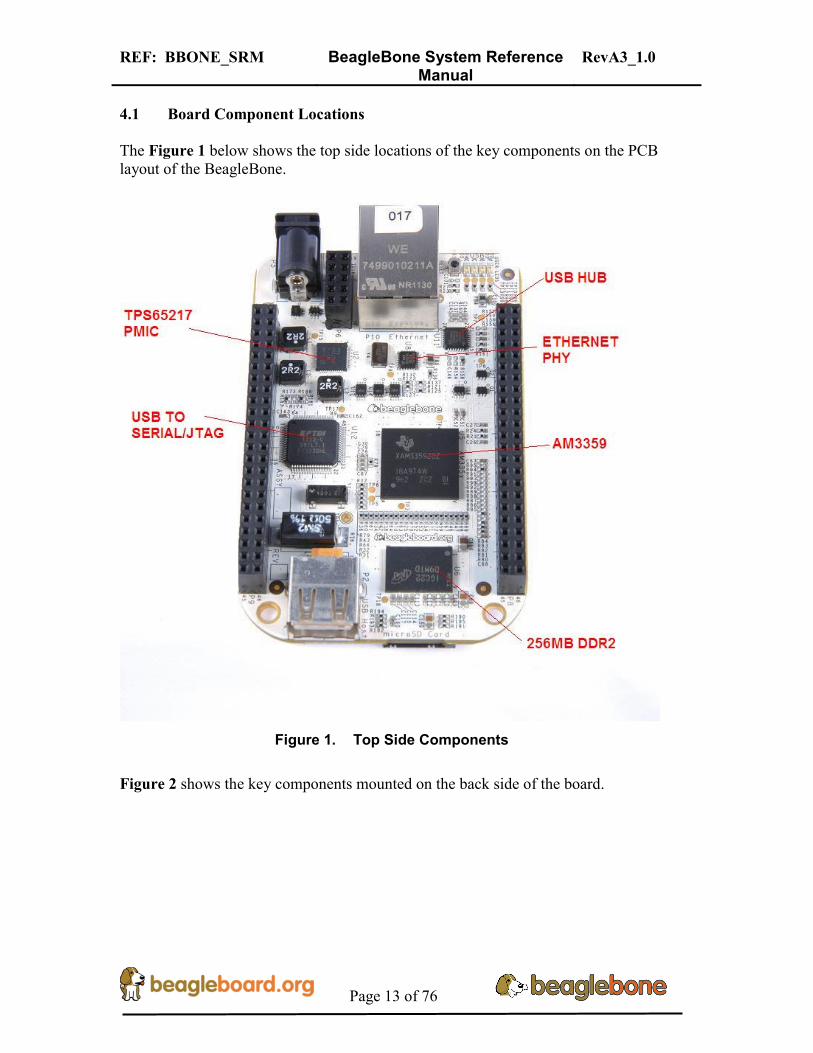
4.1 Board Component Locations The Figure 1 below shows the top side locations of the key components on the PCB layout of the BeagleBone.
Figure 1. Top Side Components
Figure 2 shows the key components mounted on the back side of the board.
REF: BBONE_SRM BeagleBone System Reference Manual
RevA3_1.0
Page 14 of 76
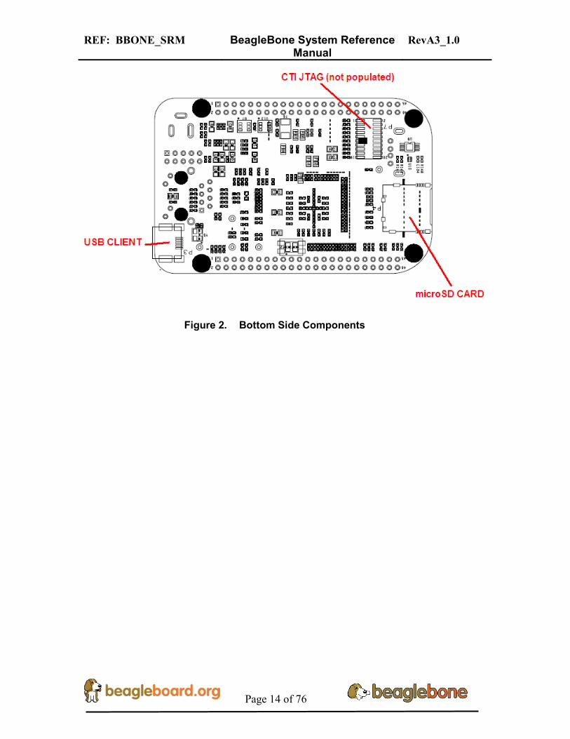
Figure 2. Bottom Side Components
REF: BBONE_SRM BeagleBone System Reference Manual
RevA3_1.0
Page 15 of 76
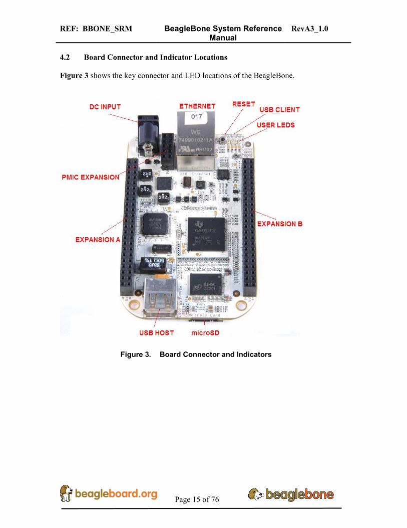
4.2 Board Connector and Indicator Locations Figure 3 shows the key connector and LED locations of the BeagleBone.
Figure 3. Board Connector and Indicators

REF: BBONE_SRM BeagleBone System Reference Manual
RevA3_1.0
Page 16 of 76
5.0 BeagleBone Design Specification This section provides a high level description of the design of the BeagleBone. 5.1 Processor The board currently uses the AM3359 processor in the 15x15 package. Actual processor speed will be determined by the actual devices supplied. The board is being released prior to the processor being in full production and as a result, has the AM3359 due to availability of those parts at this time. When changed to the AM3358, no loss of features will be experienced. 5.2 Memory As single x16 bit DDR2 memory device is used. The design supports 128MB or 256MB of memory. The standard configuration is 256MB at 400MHz. A 128MB version may be built later, but there are no definite plans for this. A single 32KB EEPROM is provided on I2C0 that holds the board information. This information includes board name, serial number, and revision information. Unused areas can be used by SW applications if desired. 5.3 Power Management The TPS65127 power management device is used along with a separate LDO to provide power to the system. 5.4 PC USB Interface The board will have an onboard USB HUB that concentrates two USB ports used on the board to one to facilitate the use of a single USB connector and cable to the PC. Support via this HUB includes:
• USB to serial debug • USB to JTAG • USB processor port access
When connected to the PC each of these will show up as ports on the PC.

REF: BBONE_SRM BeagleBone System Reference Manual
RevA3_1.0
Page 17 of 76
5.4.1 Serial Debug Port Serial debug is provided via UART0 on the processor using a dual channel FT2232H USB to serial device from FTDI to connect these signals to the USB port. Serial signals include Tx, Rx, RTS, and CTS. A single EEPROM is provided on the FT2232H to allow for the programming of the vendor information so that when connected, the board can be identified and the appropriate driver installed. 5.4.2 JTAG Port The second port on the FT2232H will be used for the JTAG port. Direct connection to the processor is made from the FT2232H. There is a JTAG header provided on the board as an option, but it is not populated. 5.4.3 USB0 Port The HUB connects direct to the USB0 port on the processor. This allows that port to be accessible from the same USB connector as the Serial and JTAG ports.
5.5 MicroSD Connector The board is equipped with a single microSD connector to act as the primary boot source for the board. A 4GB microSD card is supplied with each board. The connector will support larger capacity SD cards. 5.6 USB1 Port On the board is a single USB Type A connector with full LS/FS/HS Host support that connects to USB1 on the processor. The port can provide power on/off control and up to 500mA of current at 5V. Under USB power, the board will not be able to supply the full 500mA, but should be sufficient to supply enough current for a lower power USB device. You can use a wireless keyboard/mouse configuration or you can add a HUB for standard keyboard and mouse interfacing if required. 5.7 USB Client Port Access to USB0 is provided via the onboard USB Hub. It will show up on a PC as a standard USB device.

REF: BBONE_SRM BeagleBone System Reference Manual
RevA3_1.0
Page 18 of 76
5.8 Power Sources The board can be powered from a USB port on a PC or from an optional 5VDC power supply. The power supply is not provided with the board. The USB cable is shipped with the board. When powered from USB, the board is limited to 500 MHz. The onboard HUB + FT2232H power consumption does not leave room in the 500mA budget for the boot process. For 720 MHz operation, DC power is required. The lowest power mode is DC w/o the USB port connected, even at 720MHz. Power can be supplied via a 2.1mm x 5.5mm center connector when connected to a positive power supply rated at 5VDC +/- .1V and 1A. This is similar to the power supply as currently used on BeagleBoards and the board can be powered from a supply that was used to power the BeagleBoard. Do not apply voltages in excess of 5V to the DC input. 5.9 Reset Button When pressed and released, causes a reset of the board. Due to the small size of the switch, you will not experience a lot of travel when pushing the switch. 5.10 Indicators There are five total green LEDs on the board. Four can be controlled by the user and one static LED.
o One power LED indicates that power is applied. o Four Green LEDs that can be controlled via the SW by setting GPIO ports.
5.11 CTI JTAG Header An optional 20 pin CTI JTAG header can be provided on the board to facilitate the SW development and debugging of the board by using various JTAG emulators. In order to use the connector, series resistors must be removed to isolate the USB to JTAG feature. This header is not supplied standard on the board and the typical user will not be able to make the resistor changes.

REF: BBONE_SRM BeagleBone System Reference Manual
RevA3_1.0
Page 19 of 76
6.0 Expansion Interface This section describes the expansion interface and the features and functions available from the expansion header. 6.1 Main Board Expansion Header Two 46 pin dual row .1 x .1 female headers are supplied on the board for access to the expansion signals. Due to the number of pins, a low insertion force header has been chosen to facilitate the removal of the Capes. However, due to the large number of pins, removal can be difficult and care should be taken in the removal of the boards connected to the expansion headers. Figure 4 below is a picture of the female header used.
Figure 4. Main Board Expansion Connector
6.2 Cape Expansion Boards Each expansion board or Cape will have 2 46 pin connectors. Their exact type and configuration will vary depending on the method used. Refer to Section 8 for more details. The connectors used will be thruhole connectors. Up to four Capes can be stacked onto the BeagleBone. Each board will have the same EEPROM as is found on the main board but will be at different addresses to allow for scanning for expansion boards via the I2C bus. Each board will be equipped with a 2 position dipswitch to set the address of the board based on the stack position. It is up to the user to insure the proper setting of this dipswitch to prevent a conflict on the I2C bus.

REF: BBONE_SRM BeagleBone System Reference Manual
RevA3_1.0
Page 20 of 76
Standard expansion board size is 3.4” x 2.1”. The board will have a notch in it to act as a key to insure proper orientation. The key is around the Ethernet connector on the main board. Oversize boards, such as LCD panels, are allowed. The main board will extend out from under these boards. 6.3 Exposed Functions This section covers functionality that is accessible from the expansion header. NOTE: Not all functionality is available at the same time due to the extensive pin muxing of the signals on the processor. Please refer to the processor documentation for detailed information on the uses and functions of the pins listed in the following sections. 6.3.1 LCD A full 24 bit LCD panel can be supported. With the main board having backlight and touchscreen functionality, will simply and lower the cost of LCD expansion boards. Backlight power is limited to 25mA, so this may not be enough for larger panels. If other functions are needed on an expansion board, such as NAND support, the full 24 bit display may not be able to be supported due to the pin muxing. You can also create 16 bit LCD boards. The advantage here is that this uses fewer pins on the expansion connectors leaving more signals to be used by other expansion boards. 6.3.2 GPMC Access to the GPMC bus is provided. Depending on the configuration needed, this may result in the loss of the LCD interface. Support for a 16 bit wide NAND is provided by the expansion board. This will limit the LCD display to 16Bits. Make sure you review and understand the pin muxing option before doing a design. 6.3.3 MMC1 MMC1 signals are exposed on the expansion headers. 6.3.4 SPI There are two SPI ports available on the expansion header. SPIO0 has one CS and SPI1 has two CS signals.

REF: BBONE_SRM BeagleBone System Reference Manual
RevA3_1.0
Page 21 of 76
6.3.5 I2C
There are two I2C Ports on the expansion header, I2C1 and I2C2. I2C2 is used for the EEPROMS on the expansion boards and must always be accessible. 6.3.6 Serial Ports There are five serial ports on the expansion headers. UART1-4 has TX,Rx,RTS and CTS signals while UART5 only has TX and RX. 6.3.7 A/D Converters Seven 100K sample per second A to D converters are available on the expansion header. NOTE: Maximum voltage is 1.8V. Do not exceed this voltage. Voltage dividers should be used for voltages higher than 1.8V. In order to use these signals, level shifters will be required. These signals connect direct to the processor and care should be taken not to exceed this voltage. 6.3.8 GPIO A maximum of 66 GPIO pins are accessible from the expansion header. All of these pins are 3.3V and can be configured as inputs or outputs. Any GPIO can be used as an interrupt and is limited to two interrupts per GPIO Bank for a maximum of eight pins as interrupts. 6.3.9 CAN Bus There are two can bus interfaces available on the expansion header supporting CAN version 2 parts A and B. The TX and RX digital signals are provided. The drivers and connectors will need to be provided on a daughter card for use. 6.3.10 TIMERS There are four timer outputs on the expansion header. 6.3.11 PWM There are up to eight PWM outputs on the expansion header.
• High Resolution Outputs- up to 6 single ended. • ECAP PWM- 2 outputs

REF: BBONE_SRM BeagleBone System Reference Manual
RevA3_1.0
Page 22 of 76
7.0 Detailed Board Design This section describes the detailed design of the BeagleBone. Please be sure to reference the AM3359 datasheet and technical reference manual to gain a deeper understanding. 7.1 System Block Diagram Figure 5 is the high level system block diagram of the BeagleBone.
Figure 5. System Block Diagram
Each of these sections is discussed in more detail in the following sections. 7.2 Processor The board is designed to use the AM3358 processor in the 15 x 15 package. Initial boards that ship will have the AM3359 processor as that is the version that is currently available.
REF: BBONE_SRM BeagleBone System Reference Manual
RevA3_1.0
Page 23 of 76
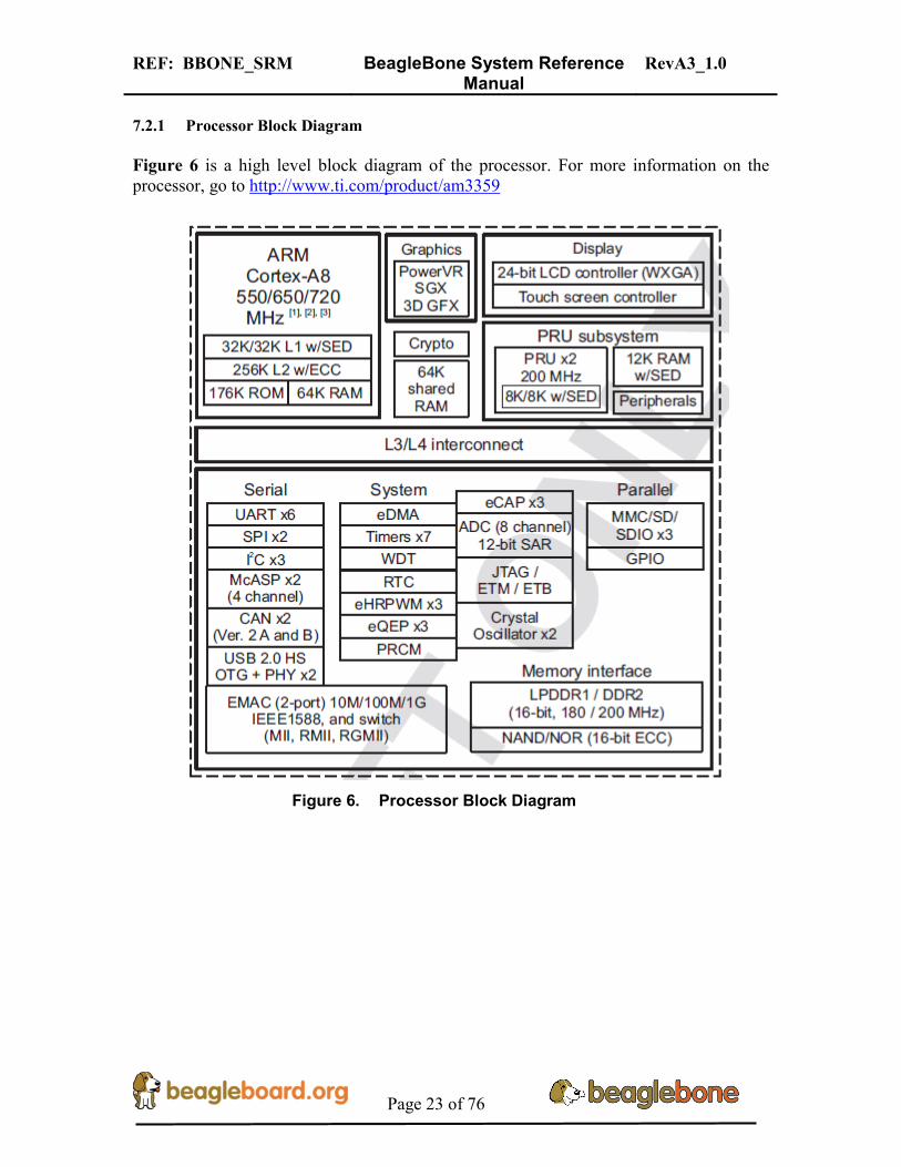
7.2.1 Processor Block Diagram Figure 6 is a high level block diagram of the processor. For more information on the processor, go to http://www.ti.com/product/am3359
Figure 6. Processor Block Diagram

REF: BBONE_SRM BeagleBone System Reference Manual
RevA3_1.0
Page 24 of 76
7.3 System Power Figure 7 is a high level block diagram of the power section design of the BeagleBone.
Figure 7. Power Subsection Block Diagram
7.3.1 TPS65217 PMIC The main Power Management IC (PMIC) in the system is the TPS65217. The TPS65217 is a single chip power management IC consisting of a linear dual-input power path, three step-down converters, four LDOs, and a high-efficiency boost converter to power two strings of up to 10 LEDs in series. The system is supplied by a USB port or DC adapter. Three high-efficiency 2.25MHz step-down converters are targeted at providing the core voltage, MPU, and memory voltage for the board. The step-down converters enter a low power mode at light load for maximum efficiency across the widest possible range of load currents. For low-noise applications the devices

REF: BBONE_SRM BeagleBone System Reference Manual
RevA3_1.0
Page 25 of 76
can be forced into fixed frequency PWM using the I2C interface. The step-down converters allow the use of small inductors and capacitors to achieve a small solution size. LDO1 and LDO2 are intended to support system-standby mode. In SLEEP state output current is limited to 100uA to reduce quiescent current whereas in normal operation they can support up to 100mA each. LDO3 and LDO4 can support up to 285mA each. By default only LDO1 is always ON but any rail can be configured to remain up in SLEEP state. Especially the DCDC converters can remain up in a low-power PFM mode to support processor Suspend mode. The TPS65217 offers flexible power-up and power-down sequencing and several house-keeping functions such as power-good output, pushbutton monitor, hardware reset function and temperature sensor to protect the battery. For more information on the TPS65217, refer to http://www.ti.com/product/tps65217 . Figure 8 is the high level block diagram of the TPS65217.

REF: BBONE_SRM BeagleBone System Reference Manual
RevA3_1.0
Page 26 of 76
Figure 8. TPS65217 Block Diagram

REF: BBONE_SRM BeagleBone System Reference Manual
RevA3_1.0
Page 27 of 76
7.3.2 5V DC Power Input Figure 9 is the design of the 5V DC input circuit to the TPS65217.
C1
4.7uF,6.3V
DGND
P5
PJ-200A
11
33
22
U1
NCP349
IN07
IN11
OUT04OUT15
EN6
GN
D2
FLAG3
DC_INU2
TPS65217B
AC10
SYS17
SYS28
DGND
DGND
VDD_5VSYS_5V
Figure 9. 5V DC Power Input
A 5VDC supply can be used to provide power to the board. The power supply current depends on how many and what type of add on boards are connected to the board. For typical use, a 5VDC supply rated at 1A should be sufficient. If heavier use of the expansion headers or USB host port is expected, then a higher current supply will be required. The connector used is a 2.1MM center positive x 5.5mm outer barrel. A NCP349 over voltage device is used to prevent the plugging in of 7 to 12 V power supplies by mistake. The NCP349 will shut down and the board will not power on. No visible indicator is provided to indicate that an over voltage condition exists. The board will not power up. The 5VDC rail is connected to the expansion header. It is possible to power the board via the expansion headers from a add-on card. The 5VDC is also available for use by the add-on cards when the power is supplied by the 5VDC jack on the board.

REF: BBONE_SRM BeagleBone System Reference Manual
RevA3_1.0
Page 28 of 76
7.3.3 USB Power The board can also be powered from the USB port. A typical USB port is limited to 500mA max. When powering from the USB port, the 5VDC is not provided to the expansion header. So daughter cards that required that rail will not have that rail available for use. Figure 10 is the design of the USB power input section.
DGND
C2
4.7uF,6.3V
U2
TPS65217B
DC12
SYS17
SYS28
SYS_5V
P3mini USB-B
D-2D+3
VB1
ID4
G2
7G
36
G15G
58
G4
9
DGND
Figure 10. USB Power Input
7.3.1 Power Source Selection The selection of either the 5VDC or the USB as the power source is handled internally to the TPS65217 and automatically switches to 5VDC power if both are connected. SW can change the power configuration via the I2C interface from the processor. In addition, the SW can read the TPS65217 and determine if the board is running on the 5VDC input or the USB input. This can be beneficial to know the capability of the board to supply current for things like operating frequency and expansion cards. It is possible to power the board from the USB input and then connect the DC power supply. The board will switch over automatically to the DC input. 7.3.2 Power Consumption The power consumption of the board varies based on power scenarios and the board boot processes. Table 3 is an analysis of the power consumption of the board in these various scenarios.
Table 3. BeagleBone Power Consumption(mA@5V)
MODE USB DC DC+USB Reset 180 60 190 UBoot 363 230 340
Kernel Booting (Peak)
502 350 470

REF: BBONE_SRM BeagleBone System Reference Manual
RevA3_1.0
Page 29 of 76
Kernel Idling 305 170 290 When the USB is connected, the FT2232 and HUB are powered up. This causes an increase in current. When the USB is not connected, these devices are in a lower power state. This is accounts for roughly 120mA of current and is the reason for the increased current when the USB is connected. The current will fluctuate as various activates occur, such as the LEDs on and SD card accesses. 7.3.3 Power Sequencing The power up process is made up of several stages and events. Figure 11 is the events that make up the power up process of the system.
Figure 11. Power Sequencing
7.3.4 TPS65217 Power Up When voltage is applied, DC or USB, the TPS65217 connects the power to the SYS output pin which drives the switchers and LDOS in the TP65217B.

REF: BBONE_SRM BeagleBone System Reference Manual
RevA3_1.0
Page 30 of 76
At power up all switchers and LDOs are off except for the VRTC LDO (1.8V), provides power to the VRTC rail. Once the RTC rail powers up, the RTC_PORZ pin of the processor can be release. Figure 12 is the circuit that controls the RTC_PORZ pin.
U17A
SN74AUP2G08
1
27
84
R171.1K,1%
U17B
SN74AUP2G08
5
63
84
C21
0.01uf ,16V
DGND
VRTC
LDO_PGOOD 2
DGND
RTC_PORZR143
0,1%,DNI
R141 10K,1%
VRTC_DET_OUT
DGND
R18
12.1K,1%
DGND
VRTC
VRTC_DETVRTC_DET
C220.01uf ,16V
DGND
VRTC_DETB
Figure 12. RTC_PORZ Control
There are actually two circuits in this design. One uses a pair of AND gates to create the RTC_PORZ signal and the other uses the LDO_PGOOD signal form the TPS65217. In the case of the AND gate circuit, once the VRTC rail comes up the circuit delays the RTC_PORZ which releases the RTC circuitry in the processor. In the case of the LDO_PGOOD signal, it is provided by the TPS65217. As this signal is 3.3V and the RTC_PORZ signal is 1.8V, a voltage divider is used. Once the LDOs are up on the TPS65217, this signal goes active. The LDOs on the TPS65217 are used to power the VRTC rail on the processor. The LDO_PGOOD version the default circuit currently used on the A3 design. It is possible on future revisions that the AND gate circuitry will be removed from the design. Once the RTC block reset is released, the processor starts the initialization process. After the RTC stabilizes, the processor launches the rest of the power up process by activating the PMIC_PWR_EN signal. This starts the TPS65217 power up process. A separate signal, PMIC_PGOOD, holds the processor reset for 20ms after all power rails are up. 7.3.5 Voltage Rails There are seven voltages supplied by the TPS65217. Each of these are described in the following sections.
7.3.5.1 VDD_1V8

REF: BBONE_SRM BeagleBone System Reference Manual
RevA3_1.0
Page 31 of 76
VDD_1V8 defaults to 1.8V on power up. The TPS65217 can deliver up to 1200mA on this rail. This rail only connects to the processor and the DDR2 memory.
7.3.5.2 VDD_MPU
VDD_MPU defaults to 1.1V on power up. This voltage can be changed under software control up to 1.25V in order to support higher processor frequencies. The TPS65217 can deliver up to 1200mA on this rail. This rail only connects to the processor.
7.3.5.3 VDD_CORE
VDD_CORE defaults to 1.1V on power up. This voltage should always be left at 1.1V. The TPS65217 can deliver up to 1200mA on this rail. This rail only connects to the processor.
7.3.5.4 VDD_3V3A
VDD_3V3A is the first of two 3.3V rails on the TPS65217. The TPS65217 can deliver up to 225mA on this rail. This rail connects to the processor I/O rail voltage, TPS65217 I/O rail, and the SD/MMC card.
7.3.5.5 VDD_3V3B
VDD_3V3B is the second of two 3.3V rails on the TPS65217. The TPS65217 can deliver up to 225 mA on this rail. This rail connects to the LAN8710, EEPROM, USB2412HUB, and FT2232.
7.3.5.6 VRTC
VRTC is the first rail to turn on during power up and is a 1.8V rail. The TPS65217 can deliver up to 100mA on this rail. This rail connects to the processor.
7.3.5.7 VLDO2
VLDO2 is a 3.3V rail that drives the power LED. This can be turned off via SW if a low current mode for the board, such as standby, is required.
7.3.6 Power Indicator LED

REF: BBONE_SRM BeagleBone System Reference Manual
RevA3_1.0
Page 32 of 76
The board has a single power indicator LED. It is controlled via 3.3V VLDO2 power rail on the TPS65217. When the TPS65217 has initialized and all switchers are on, the VLDO2 rail is activated turning on the LED. If the switchers are not initialized, for example if the processor does not enable the PWR_EN signal, the LED will not turn on. The power LED indicates that the TPS65217 is powered up. It is possible for the SW to turn off this rail to conserve power.
7.3.6.1 Expansion 3.3V LDO A separate LDO provides the 3.3V rail to the expansion headers. Figure 13 below is the design of the LDO.
VDD_3V3A
U8
TPS73701DRBR
IN8
EN5
OUT1
FB3
GND4
NC12
NC26
NC37
PAD9
R150 52.3K,1%
R189
30.1K,1%
DGND
3V3EXP_FB
SYS_VOLT
DGND
C6
4.7uF,6.3V
VDD_3V3EXP
C166 0.1uf ,16V
Figure 13. Expansion 3.3V Regulator
U8 is a TPS73710 adjustable regulator that creates the 3.3V for the expansion bus by the values of R150 and R189. The allowable current for this rail is set to 500mA based on the design of the PCB, but that depends upon the total amount of current available from the main input supply. 7.4 Current Measurement The BeagleBone has a method under which the current consumption of the board, not counting the USB Host port and expansion boards, can be measured. The voltage drop across a .1 ohm resistor is measured to determine the current consumption. Figure 14 shows the interface to the TPS65217 to measure the current. The following sections describe this circuitry in more detail. 7.4.1 SYS_5V Connection The SYS_5V rail is measured to determine the high side of the series resistor. The SYS_5V rail is connected to the MUX_OUT pin. Prior to being connected to the internal second multiplexer, the voltage is divided by 3. A 5V signal will result in a voltage of 1.66V at the MUX_OUT pin.

REF: BBONE_SRM BeagleBone System Reference Manual
RevA3_1.0
Page 33 of 76
Figure 14. Current Measurement
7.4.2 SYS_VOLT Connection The SYS_VOLT rail is measured to determine the high side of the series resistor. The SYS_VOLT rail is connected to the MUX_OUT by setting the registers inside the TPS65217. The resistors R2 and R1 are provided to keep the same voltage divider configuration as found in the SYS_5V rail located internal to the TPS65217. However, a 5V rail will give you 1.41V as opposed to the 1.66V found internal to the TPS65217. This works out to a devisor of 2.8. Be sure and work this into your final calculations. 7.4.3 MUX_OUT Connection The MUX_OUT connection is divided by 2 before being connected to the processor. The reason for this is that if the battery voltage is connected, it has no voltage divider internally. If connected it could damage the processor. When calculating the voltages for either side of the resistors, that voltage is divided by 2. Be sure and include this in your calculations. 7.4.4 Current Calculation The calculation for the current is based on .1mV is equal to 1mA. You can use the following formula to calculate the current using the voltage readings as read by the processor.
(((SYS_5V*2)*3.3)-((SYS_VOLT*2)*3.54)))/.1=Total mA.
REF: BBONE_SRM BeagleBone System Reference Manual
RevA3_1.0
Page 34 of 76
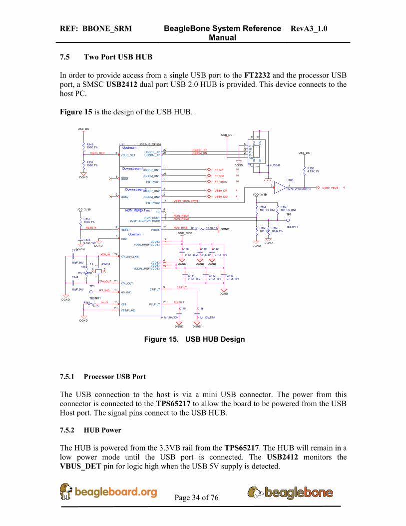
7.5 Two Port USB HUB In order to provide access from a single USB port to the FT2232 and the processor USB port, a SMSC USB2412 dual port USB 2.0 HUB is provided. This device connects to the host PC. Figure 15 is the design of the USB HUB.
DGNDHUB_BIAS
DGND
DGNDDGND
DGND
DGND
U16B
SN74LVC2G07DCK3 4
DGND
DGNDDGND
DGNDDGNDDGND
VDD_3V3B
VDD_3V3B
TP8
TESTPT1
VDD_3V3B
TP7
TESTPT1
Y5 24MHz
13
24
USB0_VBUS_PWR
FT_VBUS 10
C139
4.7uF,6.3V
VBUS_DET
CRFILT
RESETn
R149100K,1%
PLLFILT
C145
0.1uf ,10V,DNI
C146
0.1uf ,10V,DNI
R159100K,1%
NON_REM1
C140
0.1uf ,16V
C138
0.1uf ,16V
C1360.1uf ,16V
R15410K,1%,DNI
USBDP_UP
R15810K,1%
C1410.1uf ,16V
C1420.1uf ,16V
C1430.1uf ,16V
R15510K,1%,DNI
R157 12.1K,1%
R160
1M,1%,DNI
R156100K,1%
USB0_VBUS 4
R1524.75K,1%
XTALIN
DGND
XTALOUT
R151100K,1%
DGND
USB_DC
USB_DC
P3 mini USB-B
D-2 D+3
VB1
ID4
G2
7
G3
6
G15 G
58
G4
9
DGND
R1610,1%
C144
18pF,50V
C137
18pF,50V
USBDM_DN
USB0_DM 4
USB0_DP 4
rsv d3
FT_DM 10
FT_DP 10
USB_DC
HS_IND
Upstream
Dow nstream 1
Dow nstream 2
NON_REM[0:1]/nc
Common
U11 USB2412_QFN28
USBDP_UP22
USBDM_UP21
USBDP_DN11
USBDP_DN23
USBDM_DN128
USBDM_DN22
VBUS_DET18
PRTPWR17
PRTPWR211
OCS18
OCS212
RBIAS26
NC5
NON_REM113
SUSP_IND/NON_REM019
XTALIN/CLKIN24
XTALOUT23
RESET17
VSS15
TEST6
VDD3314
PLLFILT25
VDDPLLREF/VDD3327
VDDCRREF/VDD3310
CRFILT9
VSS(FLAG)29
VDD334
VDD3320
HS_IND16
NON_REM2
Figure 15. USB HUB Design
7.5.1 Processor USB Port The USB connection to the host is via a mini USB connector. The power from this connector is connected to the TPS65217 to allow the board to be powered from the USB Host port. The signal pins connect to the USB HUB.
7.5.2 HUB Power The HUB is powered from the 3.3VB rail from the TPS65217. The HUB will remain in a low power mode until the USB port is connected. The USB2412 monitors the VBUS_DET pin for logic high when the USB 5V supply is detected.
REF: BBONE_SRM BeagleBone System Reference Manual
RevA3_1.0
Page 35 of 76
7.5.3 Crystal and Reset The USB2412 uses a single 24MHZ crystal. The RESET signal is self generated from the VDD_3V3B rail to an RC network. 7.5.4 FT2232H Serial Adapter The first port of the HUB connected to the FT2232 which handles the processor serial port and JTAG and is described in the next section. The DP and DM signals from the USB2412 connect direct to the FT2232H. The FT_BUS signal is used by the FT2232H to detect the presence of the host USB port. Once the HUB is connected to the Host, this pin will go HI to indicate the presence of the USB port. 7.5.5 Processor USB Port The second port of the HUB is connected to the processor USB port 0. In order for the port to work on the processor it must first detect the presence of 5V on the VBUS pin. The USB2412 puts out a 3.3V signal on the PRTPWR2 so U16 converts that signal to a 5V logic level as required by the processor.

REF: BBONE_SRM BeagleBone System Reference Manual
RevA3_1.0
Page 36 of 76
7.6 FT2232H USB to Serial Adapter The FT2232H from FTDI provides the conversion from the USB port to the JTAG interface and Serial port to the processor. Figure 16 is the design of the FT2232H circuit.
R167 12.1K,1%
C158 0.1uf ,16V
C152
4.7uF,6.3V
C161 0.1uf ,16V DGND
VDD_FTVPHY
VDD_FTVPLL
UART0_CTS 4
UART0_TX 4
UART0_RTS 4
UART0_RX 4
R1752.2K,1%
R18110K,1%,DNI
C162
0.1uf ,16V
C163
0.1uf ,16V
VDD_3V3B
FT_VBUS 9
C164
0.1uf ,16V
VDD_3V3B
DGNDFT_RESETn
F_EEDO
UT
XTIN
XTOUT
Y612.000MHz50ppm
U13
93LC56B_SOT23-6
CS5
SK4
DIN3
DOUT1
GND2
VCC6
F_EEDATAF_EESK
F_EECS
C147 0.1uf ,16V
C148 0.1uf ,16V
R1882.2K,1%
VDD_1V8FT
R187 10K,1%
R173 10K,1%
F_ADBUS2F_ADBUS1F_ADBUS0
F_ADBUS6
F_ADBUS5
F_ADBUS4F_ADBUS3
R174 10K,1%
F_ADBUS7C153 27pF,50V
VDD_3V3B
DGND
C155 27pF,50V
R164 0,1%
R166 0,1%R165 0,1%
R169 0,1%
R170 0,1%
R168 0,1%
R172 0,1%
R171 0,1%
DGND
DGND
FB6150OHM800mA
1 2
DGND
DGND
DGND
FT_DP9FT_DM9
U12
FT2232LQFN64
VREGOUT49
USBDP8 USBDM7
OSCIN2
OSC03
RESET14
EECS63
EECLK62
EEDATA61
TEST13
VPH
Y4
VCO
RE
B37
VCO
RE
A64
VCC
IOA
20
VCC
IOB
31
ADBUS016
ADBUS117
ADBUS218
ADBUS319
ADBUS421
ADBUS522
ADBUS623
ADBUS724
ACBUS026
ACBUS127
ACBUS228
ACBUS329
BDBUS038
BDBUS139
BDBUS240
BDBUS341
BDBUS443
BDBUS544
BDBUS645
BDBUS746
BCBUS048
BCBUS152
BCBUS253
BCBUS354
SUSPEND36
PWREN60
AGN
D10
GN
D4
25
GN
D3
35
GN
D2
47
GN
D1
51
ACBUS430
ACBUS532
ACBUS633
ACBUS734
BCBUS455
BCBUS557
BCBUS658
BCBUS759
GN
D6
11G
ND
75
GN
D8
1VREGIN
50
VCC
IOB
42
VCC
IOD
56
VCO
REC
12VP
LL9
GN
D5
15
REF6
C150 0.1uf ,16V
C151 0.1uf ,16V
VDD_3V3B
FB7150OHM800mA
1 2
FB8150OHM800mA
1 2 VDD_FTREGIN
DGND FT_REF
VDD_3V3B
DGND Figure 16. FT2232H Design
7.6.1 EEPROM U13 is a EEPROM that tells U12 the configuration of the device and the I/O pins. In order for the FT2232H to operate properly, this device must be programmed. Using the tools provided by FTDI makes this process straight forward.

REF: BBONE_SRM BeagleBone System Reference Manual
RevA3_1.0
Page 37 of 76
7.6.2 JTAG Using a parallel I/O mode, the FT2232H can be used to access the JTAG signals on the processor. At USB 2.0 speeds, the throughput is very good, and should provide connectivity to several popular debug environments including Code Composer Studio 7.6.3 Serial Port Access to UART0 is provided by the FT2232H via the USB port. Signals available are TX, RX, RTS, and CTS. 7.7 256MB DDR2 Memory The board comes standard with 256MB DDR SDRAM configured as a single 128M x 16 device. The design will also support a single 64M x 16 device for 128MB of memory. The memory size cannot be extended past 256MB. The design uses a single MT47H128M16RT-25E:C 400MHZ memory from Micron which comes in an 84-Ball 9.0mm x 12.5mm FBGA package. Table 4 below is the addressing configuration of the device.
Table 4. DDR Addressing
Figure 17 is the functional block diagram of the DDR2 memory device.
REF: BBONE_SRM BeagleBone System Reference Manual
RevA3_1.0
Page 38 of 76
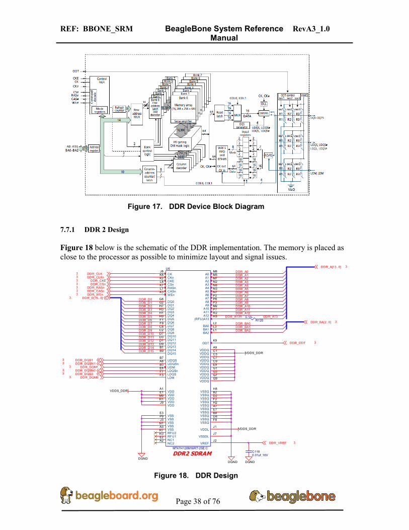
Figure 17. DDR Device Block Diagram
7.7.1 DDR 2 Design Figure 18 below is the schematic of the DDR implementation. The memory is placed as close to the processor as possible to minimize layout and signal issues.
DDR_DQS03DDR_DQSN03
DDR_DQS13
R1200,1%
DDR_DQSN13
DDR_A13R
C1180.01uf ,16V
DGND
DDR2 SDRAMDGND
DGND
DDR_ODT 3
DDR_VREF 3
U6
MT47H128M16RT-25E:C
CKJ8
CKnK8
CKEK2
CSnL8
RASnK7
CASnL7
WEnK3
A0M8
A1M3
A2M7
A3N2
A4N8
A5N3
A6N7
A7P2
A8P8
A9P3
A10M2
A11P7
A12R2
(RFU)A13R8
BA0L2
BA1L3
BA2L1
DQ0G8
DQ1G2
DQ2H7
DQ3H3
DQ4H1
DQ5H9
DQ6F1
DQ7F9
ODTK9
VSSA3
VSSQB2
VSSQE7
VSSQD2
VSSQD8
VSSDLJ7
VSSQA7
VDDQA9
VDDQC1
VDDQC3
VDDQC9
VREFJ2
VDDLJ1
VDDA1
VDDR1
UDQSnA8
UDMB3
NC2A2
UDQSB7
DQ14B1
DQ15B9
DQ9C2 DQ8C8
DQ12D1 DQ11D3 DQ10D7
DQ13D9
VDDE1
VSSE3
LDQSnE8
VDDQC7
VSSQF2
LDMF3
VSSQB8
VDDQG3VDDQG1
VSSQF8
VSSJ3
VDDJ9
VDDM9
VSSN1
VSSP9
RFU1R3
NC1E2
VDDQG7
VDDQG9
VSSQH2
VSSQH8
LDQSF7
VDDQE9
RFU2R7
VDDS_DDR
DDR_A3
VDDS_DDR
VDDS_DDR
DDR_A4
DDR_A0DDR_A1
DDR_A5DDR_A6
DDR_A2
DDR_A8DDR_A9
DDR_A11DDR_A12
DDR_A7
DDR_A13
DDR_A10
DDR_A[13..0] 3
DDR_BA1DDR_BA2
DDR_BA0 DDR_BA[2..0] 3
DDR_D3
DDR_D1DDR_D0
DDR_D6DDR_D7
DDR_D4DDR_D5
DDR_D2
DDR_D[15..0]3
DDR_D14
DDR_D9DDR_D10DDR_D11DDR_D12
DDR_D8
DDR_D15
DDR_D13
DDR_DQM13
DDR_DQM03
DDR_CLKn3DDR_CLK3
DDR_CSn3DDR_CKE3
DDR_CASn3DDR_WEn3
DDR_RASn3
Figure 18. DDR Design

REF: BBONE_SRM BeagleBone System Reference Manual
RevA3_1.0
Page 39 of 76
The DDR2 connects direct to the processor and no external interface devices are required. Power is supplied to the DDR2 via the 1.8V rail on the TPS65217. 7.7.2 DDR VTP Termination Resistor There is a requirement for a 50 ohm 1% termination resistor, R76, on the DDR interface. You will notice that the one used on the board design is a 50W wire wound resistor. The reason for this is cost. This resistor can be expensive and at the time of the design, this was the least expensive one package available. On the Rev A4 design, we added two more resistors, R217 and R218, to allow for a 0603 and 0805 package for applications where space is critical and to give us more options where parts availability is concerned. 7.7.3 User LEDs Four user LEDS are provided via GPIO pins on the processor. Figure 19 below shows the LED circuitry.
R116100K,1%
R117100K,1%
R118100K,1% R119
100K,1%
GRN
D2
598-8170-107F
GRN
D3
598-8170-107F
GRN
D4
598-8170-107F
GRN
D5
598-8170-107F
DGNDDGND
47k10k Q1A
DMC56404
16
2 47k10k Q2A
DMC56404
16
2
47k10k Q1B
DMC56404
43
5
DGND
47k10k Q2B
DMC564044
3
5
DGND
DGNDDGND
DGNDDGND
USR13
USR03
USR33USR23
LED
AC
LED
BC
LED
CC
LED
DC
USR0 USR3USR2USR1R97470,5%
R96470,5%
R98470,5%
R99470,5%
SYS_5V
FB4150OHM800mA
12
VDD_LED
C100
4.7uF,6.3V
DGND
Figure 19. User LEDS
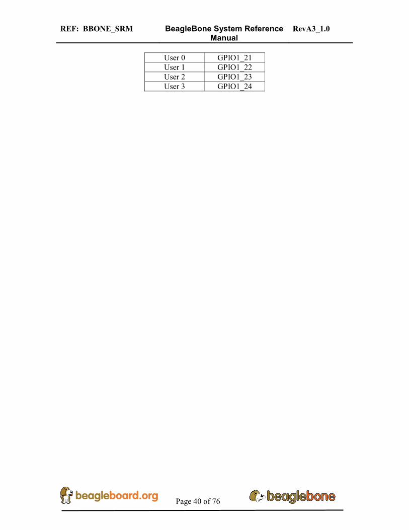
Q1 and Q2 provide level shifting from the processor to drive the LEDs that are connected the SYS_5V rail. FB4 provides noise immunity to the system by the LEDS which can be a source of noise back into the system rail. Each LED is controlled by setting the appropriate GPIO bit HI. At power up all LEDs are off. Table 5 is the GPIO USER LED assignments.
Table 5. User LED Control
LED GPIO
REF: BBONE_SRM BeagleBone System Reference Manual
RevA3_1.0
Page 40 of 76
User 0 GPIO1_21 User 1 GPIO1_22 User 2 GPIO1_23 User 3 GPIO1_24

REF: BBONE_SRM BeagleBone System Reference Manual
RevA3_1.0
Page 41 of 76
7.8 10/100 Ethernet The 10/100 Ethernet uses a SMSC LAN8710A Ethernet PHY and interfaces to the processor using the MII interface. This section covers that design. 7.8.1 Ethernet PHY Design Figure 20 below is the design of the 10/100 PHY section of the board.
R14512.1K,1%
YELA
FB5150OHM800mA1 2
R13
049
.9,1
%
R13
349
.9,1
%
R13
449
.9,1
%
C126
15pF,DNI
C127
15pF,DNI
RXN
C128
15pF,DNI
C129
15pF,DNI
RXP
R12
949
.9,1
%
VDD_3V3B
VDD_PHYA
VDD_PHYA
DGNDDGND
DGND
DGND
DGNDDGND
DGND
DGND
DGND
DGND
DGND
PHY_VDDCR
DGND
C1220.1uf ,16V
DGND DGND
C1200.1uf ,16V
C1230.1uf ,16V
C1190.1uf ,16V
C132
30pF,50V
C131
30pF,50V
SYS_RESETn11,3
RBIASPHY_XTAL2
RXER/PHYAD0
RXD1/MODE1RXD0/MODE0
C124470pF50V5%
PHYXY4
25.000MHzXTAL2_5X3P2_SMD
12
PHY_XTAL1
CRS_DV/MODE2
R135 100,1%R132 100,1%
TXP
R137 100,1%R136 100,1%
TXN
R14410,1%
R139 100,1%
C1251uF,10V
R13
11.
5K,5
%
R199 0,1%
R200 0,1%,DNI
R1401M,1%,DNI
REFCLKO
C1214.7uF,6.3V
GRNA
RMII1_RXCLK4
U15
LAN8710A
QFN32_5X5MM_EP3P3MM
MDIO16
MDC17
RXD3/PHYAD28
RXD2/RMIISEL9
RXD1/MODE110
RXD0/MODE011
RXDV26
RXCLK/PHYAD17
RXER/RXD4/PHYAD013
TXCLK20
TXEN21
TXD022
TXD123
TXD224
TXD325
COL/CRS_DV/MODE215
CRS14
nRST19
XTAL1/CLKIN5
XTAL24
GN
D_E
P33
RBIAS32
VD
DIO
12
VDD
1A27
VDD
2A1
VDD
CR
6RXP
31
RXN30
TXN28TXP29
nINT/TXER/TXD418
LED2/nINTSEL2LED1/REGOFF3
R205 100,1%RXD2/RMIISELR153 100,1%
RMII1_RXD34 RXD3/PHYAD2
RMII1_RXD24
RCLKIN
RMII1_TXD34RMII1_TXD24
R206 100,1%RMII1_TXCLK4 TXCLK
R207 100,1%RMII1_COL4 COL/CRS_DV/MODE2
R208 100,1%RMII1_RXDV4 RXDV
RMII1_CRS_DV4
RMII1_RXD04RMII1_RXD14
MDIO_CLK4
RMII1_TXEN4
RMII1_RXERR4
MDIO_DATA4
RMII1_TXD04RMII1_TXD14
RMII1_REFCLK4 R209 10,1%,DNI
GRN_C
TXP
RXNRXP
C167
0.022uF,10V
TXN
DGND
DGND
TCT_RCT
R2020,1%
ESD_RING
DGND
R217
.1,0805
P11
WE_7499010211A
TCT5
TD+3
TD-6
RD+1
RD-2
RCT4
YELC11
YELA12
GRNC10
GRNA9
GND8
SHD113
SHD214
NC7
DGND
VDD_PHYA
YELAR218 470,5%
GRNA
YEL_C
R219 470,5%
Figure 20. 10/100 Ethernet PHY Design

REF: BBONE_SRM BeagleBone System Reference Manual
RevA3_1.0
Page 42 of 76
7.8.2 Processor Signal Description The Table 6 describes the signals between the processor and the LAN8710A. The BALL column is the pin number on the processor. The SIGNAL name is the generic name of the signal on the processor. The PHY column is the pin number of the PHY.
Table 6. Processor Ethernet Signals
7.8.3 Clocking Mode The LAN8710A provides the clock to the processor and is generated by the onboard 25MHz crystal Y4. There are independent clocks for the transmit channel (MII Transmit Clock) and for the receive channel (MII Receive clock). 7.8.4 PHY Mode The PHY operates in the 10/100 mode with auto negotiation enabled. This is set via the resistors as described in Figure 21 which are sampled by the PHY when coming out of reset. It is possible for SW to override this setting if required by setting these bits via the MDIO channel.

REF: BBONE_SRM BeagleBone System Reference Manual
RevA3_1.0
Page 43 of 76
R21
210
K,1
%
R21
310
K,1%
,DN
I
RXD3/PHYAD2
nINT/RXCLK/PHYAD1
R21
410
K,1
%
R21
510
K,1
%,D
NI
R21
610
K,1
%
VDD_3V3B
DGND
RMISEL PHYAD0PHYAD1PHYAD0 MODE0
CRS_DV/MODE2
MODE2 MODE1
RXD1/MODE1
RXER/PHYAD0
R12
310
K,1%
RXD0/MODE0
R12
210
K,1
% R12
410
K,1
%
R12
510
K,1
%
R19
810
K,1%
,DN
I
R5
10K,
1%,D
NI
R12
710
K,1
%,D
NI
R12
610
K,1%
,DN
I
R21
110
K,1
%,D
NI
RXD2/RMIISEL
Figure 21. 10/100 Ethernet PHY Default Settings
By adding pull up or pull down resistors, the default mode of the PHY can be set via HW. Seven pairs of resistors are provided on the board to set the mode. Pins MODE0-1 set the operating mode of the PHY. Default mode is 111 as set by the populating of R122-124. This enables all operating modes and auto negotiation. PHYAD0-2 sets the default address of the PHY. Populating R124-R126 set the default of 0. It is not expected to be set to anything other than this, but the other option was enabled just in case. RMIISEL sets the mode to RMII if R211 is installed. MII is the default mode used in this design, so R212 needs to be installed and R211 is not to be installed.

REF: BBONE_SRM BeagleBone System Reference Manual
RevA3_1.0
Page 44 of 76
7.8.5 MDIO Interface The MDIO interface is the control channel interface between the processor and the LAN8710A. Via this interface all of the internal PHY registers can be read and set by the processor and important status information can be read. 7.8.6 PHY Reset The PHY reset signal is connected to the main board reset and is reset on power up. 7.8.7 Status LEDs They Ethernet connector has a Yellow and Green LED. The Green LED will be on when a link is established. It flashes off when data is transferred. The Yellow LED is off when the link is 100M and on when it is 10M. This operation is reversed from normal. Whenever the next revision of the board occurs, this will be fixed. 7.8.8 Power The PHY is powered via the 3.3VB rail from the TPS65217. A filter is provided between the 3.3VB rail and the PHY. The internal LDO is used to power the internal rails. 7.9 USB Host A single USB Host port is provided on the board. It is driven by USB port 1 of the processor. The port can deliver up to 500mA of current provided that much current is available from the power supply. In the scenario where the board is totally powered from the USB input, the power supplied will be much less and dependent on how much current is available after driving the board and any daughter cards that may be attached. 7.9.1 USB Host design The board has a single USB host connector accessible via P2 a type A female connector. Figure 22 below is the USB Host design.
R14810K,1%
R14710K,1%
R1460,1%
U9
TPS2051 (DGN)
GND1
IN2
IN3
EN4
OUT6OUT7OUT8
OC5
PAD9
DGNDDGND
DGND
USB1_DM4USB1_DP4
USB1_OC 3
DGND
DGND
DGND
DGND
VDD_3V3B
SHIELD
SHIELD
VBUSD-D+GND
P2USB-A Conn. - 87520-xx1xx
1
32
4
5
6USB1_ID4
C1340.01uf ,16V
USB1_DRVVBUS4U10
TPD4S012
D+1
D-2
VBUS6
GND4
NC5
ID3
+C133
100uF,6.3V
SYS_5V
USB1_VBUS 4
Figure 22. USB Host Design

REF: BBONE_SRM BeagleBone System Reference Manual
RevA3_1.0
Page 45 of 76
The USB port on the processor is an OTG port. In order to force the host function needed, the ID pin, USB_ID, is grounded permanently by R146. U9, a TPS2051, is the power switch that controls the 5VDC to the USB port. It is turned on by the processor via USB1_DRVVBUS signal. The USB1_VBUS signal is a confirmation back to the processor that the switch is activated and that 5V is connected to the USB Host connector. In the event of an over current condition, the switch will signal the processor of the event, via USB1_OC, and the switch will shut down. R148 is a pullup to provide the HI voltage level because the OC signal on U9 is an open drain pin. C133 provides extra current when devices are inserted into the connector per the USB specification. The amount of current the switch can provide is limited by the available current from the main power source. In order to handle high current devices, you need to power the board from the DC input connector and not USB. Powering from USB can in, most cases, supply enough current to run a thumbdrive or low current device. U10 is an ESD protection device intended to protect the processor. 7.10 SD Connector
The board is populated with a microSD small form factor SD slot. It will support High capacity cards. The voltage rail for the connector is 3.3VA. A card detector output is provided from the connector to the CD/EMU4 signal. Figure 23 shows the connections to the microSD connector.
MMC0_DAT23MMC0_DAT33 SD_CDDGND
uSD ConnectorDGND
microSD
P4
SCHA5B0200
DAT21
CD/DAT32
CMD3
VDD4
CLOCK5
VSS6
DAT07
DAT18
GND9
CD10
GND311
GND412
GND513
GND614
GND715
GND816
MMC0_CLKO3
R19
010
K,1
%
MMC0_DAT13MMC0_DAT03
R19
110
K,1
%
MMC0_CMD3
R19
210
K,1
%
R19
310
K,1
%
R196 10K,1%
R19
410
K,1
%
R19
510
K,1
%
C1600.1uf ,16V
VDD_3V3
R197
0,1%
CD/EMU410,4
VDD_3V3
C159
10uF,10V
DGND
Figure 23. SD Connector Design
There are pullup resistors on all the signals to provide additional drive strength and to increase the rise time of the signals. The SD_CD is the signal that indicates to the processor that the card is inserted. The signal is a contact point on the connector and R196 provides the logic hi signal that is grounded whenever there is no card inserted.

REF: BBONE_SRM BeagleBone System Reference Manual
RevA3_1.0
Page 46 of 76
When the card is inserted, the signal will go high. R197 is provided as an option to allow this signal to be removed from the processor for use as the EMU4 signal by the optional JTAG connector. The connector is located on the bottom side of the board and the card should be inserted with the label side up and the contact pins down. This connector is a Push-Push connector. To insert the card push the card in until it clicks and then release. To remove the card, push the card in and the connector will release the card and eject the card. WARNING: DO NOT PULL THE CARD OUT TO REMOVE IT OR YOU MAY DAMAGE THE CONNECTOR. 7.11 EEPROM The BeagleBone is equipped with a single CAT24C256W EEPROM to allow the SW to identify the board. Table 7 below defined the contents of the EERPOM.
Table 7. EEPROM Contents
Name Size (bytes) Contents
Header 4 0xAA, 0x55, 0x33, EE
Board Name 8 Name for board in ASCII: A335BONE
Version 4 Hardware version code for board in ASCII: 00A3
Serial Number 12 Serial number of the board. This is a 12 character string which is: WWYY4P16nnnn
where: WW = 2 digit week of the year of production YY = 2 digit year of production
nnnn = incrementing board number
Configuration Option
32 Codes to show the configuration setup on this board. 0000000000000000000000000000000
RSVD 6 000000
RSVD 6 000000
RSVD 6 000000
Available 32702 Available space for other non-volatile codes/data Figure 24 is the design of the EEPROM circuit.

REF: BBONE_SRM BeagleBone System Reference Manual
RevA3_1.0
Page 47 of 76
I2C0_SDA2,4
DGND
VDD_3V3B
C1020.1uf ,16V
I2C0_SCL2,4
32KX8 (256Kb)
U7
CAT24C256W
A01
A12
A23
SCL6
SDA5 VCC
8
VSS4
WP7
DGND
R210 10K,1%,DNIWP
Figure 24. EEPROM Design
The EEPROM is accessed by the processor using the I2C 0 bus. The EEPROM is not write protected. R21 if installed would invoke the write protection. The WP pin has an internal pulldown on it so that if removed the pin is grounded. The first 48 locations should not be written to if you choose to use the extras storage space in the EEPROM. If you do, it could prevent the board from booting properly as the SW uses this information to determine how to set up the board.

REF: BBONE_SRM BeagleBone System Reference Manual
RevA3_1.0
Page 48 of 76
7.12 Expansion Headers The expansion interface on the board is comprised of two 46 pin connectors. All signals on the expansion headers are 3.3V unless otherwise indicated. NOTE: Do not connect 5V logic level signals to these pins or the board will be damaged. 7.12.1 Expansion Header P8 Table 8 shows the default pinout of the P8 expansion header. Other signals can be connected to this connector based on setting the pin mux on the processor, but this is the default settings on power up. The SW is responsible for setting the default function of each pin.
Table 8. Expansion Header P8 Pinout
SIGNAL NAME PROC CONN PROC SIGNAL NAME GND 1 2 GND
GPIO1_6 R9 3 4 T9 GPIO1_7
GPIO1_2 R8 5 6 T8 GPIO1_3
TIMER4 R7 7 8 T7 TIMER7
TIMER5 T6 9 10 U6 TIMER6
GPIO1_13 R12 11 12 T12 GPIO1_12
EHRPWM2B T10 13 14 T11 GPIO0_26
GPIO1_15 U13 15 16 V13 GPIO1_14
GPIO0_27 U12 17 18 V12 GPIO2_1 EHRPWM2A U10 19 20 V9 GPIO1_31
GPIO1_30 U9 21 22 V8 GPIO1_5
GPIO1_4 U8 23 24 V7 GPIO1_1
GPIO1_0 U7 25 26 V6 GPIO1_29
GPIO2_22 U5 27 28 V5 GPIO2_24
GPIO2_23 R5 29 30 R6 GPIO2_25
UART5_CTSN V4 31 32 T5 UART5_RTSN
UART4_RTSN V3 33 34 U4 UART3_RTSN
UART4_CTSN V2 35 36 U3 UART3_CTSN
UART5_TXD U1 37 38 U2 UART5_RXD
GPIO2_12 T3 39 40 T4 GPIO2_13
GPIO2_10 T1 41 42 T2 GPIO2_11
GPIO2_8 R3 43 44 R4 GPIO2_9
GPIO2_6 R1 45 46 R2 GPIO2_7

REF: BBONE_SRM BeagleBone System Reference Manual
RevA3_1.0
Page 49 of 76
7.12.2 P8 Signal Pin Mux Options Table 9 shows the other signals that can be connected to each pin of P8 based on the settings of the registers in the processor for modes 0-3.
Table 9. P8 Mux Options Modes 0-3 PIN PROC NAME MODE0 MODE1 MODE2 MODE3
1 GND
2 GND
3 R9 GPIO1_6 gpmc_ad6 mmc1_dat6 4 T9 GPIO1_7 gpmc_ad7 mmc1_dat7 5 R8 GPIO1_2 gpmc_ad2 mmc1_dat2
6 T8 GPIO1_3 gpmc_ad3 mmc1_dat6
7 R7 TIMER4 gpmc_advn_ale timer4
8 T7 TIMER7 gpmc_oen_ren timer7
9 T6 TIMER5 gpmc_be0n_cle timer5
10 U6 TIMER6 gpmc_wen timer6
11 R12 GPIO1_13 gpmc_ad13 lcd_data18 mmc1_dat5 mmc2_dat1
12 T12 GPIO1_12 GPMC_AD12 LCD_DATA19 MMC1_DAT4 MMC2_DAT0
13 T10 EHRPWM2B gpmc_ad9 lcd_data22 mmc1_dat1 mmc2_dat5
14 T11 GPIO0_26 gpmc_ad10 lcd_data21 mmc1_dat2 mmc2_dat6
15 U13 GPIO1_15 gpmc_ad15 lcd_data16 mmc1_dat7 mmc2_dat3
16 V13 GPIO1_14 gpmc_ad14 lcd_data17 mmc1_dat6 mmc2_dat2
17 U12 GPIO0_27 gpmc_ad11 lcd_data20 mmc1_dat3 mmc2_dat7
18 V12 GPIO2_1 gpmc_clk_mux0 lcd_memory_clk gpmc_wait1 mmc2_clk
19 U10 EHRPWM2A gpmc_ad8 lcd_data23 mmc1_dat0 mmc2_dat4
20 V9 GPIO1_31 gpmc_csn2 gpmc_be1n mmc1_cmd
21 U9 GPIO1_30 gpmc_csn1 gpmc_clk mmc1_clk
22 V8 GPIO1_5 gpmc_ad5 mmc1_dat5
23 U8 GPIO1_4 gpmc_ad4 mmc1_dat3
24 V7 GPIO1_1 gpmc_ad1 mmc1_dat1
25 U7 GPIO1_0 gpmc_ad0 mmc1_dat0
26 V6 GPIO1_29 gpmc_csn0
27 U5 GPIO2_22 lcd_vsync gpmc_a8
28 V5 GPIO2_24 lcd_pclk gpmc_a10
29 R5 GPIO2_23 lcd_hsync gpmc_a9
30 R6 GPIO2_25 lcd_ac_bias_en gpmc_a11
31 V4 UART5_CTSN lcd_data14 gpmc_a18 eQEP1_index mcasp0_axr1
32 T5 UART5_RTSN lcd_data15 gpmc_a19 eQEP1_strobe mcasp0_ahclkx
33 V3 UART4_RTSN lcd_data13 gpmc_a17 eQEP1B_in mcasp0_fsr
34 U4 UART3_RTSN lcd_data11 gpmc_a15 ehrpwm1B mcasp0_ahclkr
35 V2 UART4_CTSN lcd_data12 gpmc_a16 eQEP1A_in mcasp0_aclkr

REF: BBONE_SRM BeagleBone System Reference Manual
RevA3_1.0
Page 50 of 76
PIN PROC NAME MODE0 MODE1 MODE2 MODE3
36 U3 UART3_CTSN lcd_data10 gpmc_a14 ehrpwm1A mcasp0_axr0
37 U1 UART5_TXD lcd_data8 gpmc_a12 ehrpwm1_tripzone_in mcasp0_aclkx
38 U2 UART5_RXD lcd_data9 gpmc_a13 ehrpwm0_synco mcasp0_fsx
39 T3 GPIO2_12 lcd_data6 gpmc_a6 eQEP2_index
40 T4 GPIO2_13 lcd_data7 gpmc_a7 eQEP2_strobe
41 T1 GPIO2_10 lcd_data4 gpmc_a4 eQEP2A_in
42 T2 GPIO2_11 lcd_data5 gpmc_a5 eQEP2B_in
43 R3 GPIO2_8 lcd_data2 gpmc_a2 ehrpwm2_tripzone_in
44 R4 GPIO2_9 lcd_data3 gpmc_a3 ehrpwm0_synco
45 R1 GPIO2_6 lcd_data0 gpmc_a0 ehrpwm2A
46 R2 GPIO2_7 lcd_data1 gpmc_a1 ehrpwm2B There are some signals that have not been listed here. Refer to the processor documentation for more information on these pins and detailed descriptions of all of the pins listed. In some cases there may not be enough signals to complete a group of signals that may be required to implement a total interface. The PROC column is the pin number on the processor. The PIN column is the pin number on the expansion header. The MODE columns are the mode setting for each pin. Setting each mode to align with the mode column will give that function on that pin.

REF: BBONE_SRM BeagleBone System Reference Manual
RevA3_1.0
Page 51 of 76
Table 10 shows the other P8 signals for modes 4-7.
Table 10. P8 Mux Options Modes 4-7
PIN PROC NAME MODE4 MODE5 MODE6 MODE7
1 GND
2 GND
3 R9 GPIO1_6 gpio1[6]
4 T9 GPIO1_7 gpio1[7]
5 R8 GPIO1_2 gpio1[2]
6 T8 GPIO1_3 gpio1[3]
7 R7 TIMER4 gpio2[2]
8 T7 TIMER7 gpio2[3]
9 T6 TIMER5 gpio2[5]
10 U6 TIMER6 gpio2[4]
11 R12 GPIO1_13 eQEP2B_in gpio1[13]
12 T12 GPIO1_12 EQEP2A_IN gpio1[12]
13 T10 EHRPWM2B ehrpwm2B gpio0[23]
14 T11 GPIO0_26 ehrpwm2_tripzone_in gpio0[26]
15 U13 GPIO1_15 eQEP2_strobe gpio1[15]
16 V13 GPIO1_14 eQEP2_index gpio1[14]
17 U12 GPIO0_27 ehrpwm0_synco gpio0[27]
18 V12 GPIO2_1 mcasp0_fsr gpio2[1]
19 U10 EHRPWM2A ehrpwm2A gpio0[22]
20 V9 GPIO1_31 gpio1[31]
21 U9 GPIO1_30 gpio1[30]
22 V8 GPIO1_5 gpio1[5]
23 U8 GPIO1_4 gpio1[4]
24 V7 GPIO1_1 gpio1[1]
25 U7 GPIO1_0 gpio1[0]
26 V6 GPIO1_29 gpio1[29]
27 U5 GPIO2_22 gpio2[22]
28 V5 GPIO2_24 gpio2[24]
29 R5 GPIO2_23 gpio2[23]
30 R6 GPIO2_25 gpio2[25]
31 V4 UART5_CTSN uart5_rxd uart5_ctsn gpio0[10]
32 T5 UART5_RTSN mcasp0_axr3 uart5_rtsn gpio0[11]
33 V3 UART4_RTSN mcasp0_axr3 uart4_rtsn gpio0[9]
34 U4 UART3_RTSN mcasp0_axr2 uart3_rtsn gpio2[17]
35 V2 UART4_CTSN mcasp0_axr2 uart4_ctsn gpio0[8]
36 U3 UART3_CTSN uart3_ctsn gpio2[16]
37 U1 UART5_TXD uart5_txd uart2_ctsn gpio2[14]

REF: BBONE_SRM BeagleBone System Reference Manual
RevA3_1.0
Page 52 of 76
PIN PROC NAME MODE4 MODE5 MODE6 MODE7
38 U2 UART5_RXD uart5_rxd uart2_rtsn gpio2[15]
39 T3 GPIO2_12 gpio2[12]
40 T4 GPIO2_13 pr1_edio_data_out7 gpio2[13]
41 T1 GPIO2_10 gpio2[10]
42 T2 GPIO2_11 gpio2[11]
43 R3 GPIO2_8 gpio2[8]
44 R4 GPIO2_9 gpio2[9]
45 R1 GPIO2_6 gpio2[6]
46 R2 GPIO2_7 gpio2[7] There are some signals that have not been listed here. Refer to the processor documentation for more information on these pins and detailed descriptions of all of the pins listed. In some cases there may not be enough signals to complete a group of signals that may be required to implement a total interface. The PROC column is the pin number on the processor. The PIN column is the pin number on the expansion header. The MODE columns are the mode setting for each pin. Setting each mode to align with the mode column will give that function on that pin.

REF: BBONE_SRM BeagleBone System Reference Manual
RevA3_1.0
Page 53 of 76
7.12.3 Expansion Header P9 Table 11 lists the signals on connector P9. Other signals can be connected to this connector based on setting the pin mux on the processor, but this is the default settings on power up. Signals highlighted in yellow are changes from the previous revision of the SRM.
Table 11. Expansion Header P9 Pinout
SIGNAL NAME PIN CONN PIN SIGNAL NAME GND 1 2 GND
VDD_3V3EXP 3 4 VDD_3V3EXP
VDD_5V 5 6 VDD_5V
SYS_5V 7 8 SYS_5V
PWR_BUT* 9 10 A10 SYS_RESETn
UART4_RXD T17 11 12 U18 GPIO1_28
UART4_TXD U17 13 14 U14 EHRPWM1A
GPIO1_16 R13 15 16 T14 EHRPWM1B
I2C1_SCL A16 17 18 B16 I2C1_SDA
I2C2_SCL D17 19 20 D18 I2C2_SDA
UART2_TXD B17 21 22 A17 UART2_RXD
GPIO1_17 V14 23 24 D15 UART1_TXD
GPIO3_21 A14 25 26 D16 UART1_RXD
GPIO3_19 C13 27 28 C12 SPI1_CS0
SPI1_D0 B13 29 30 D12 SPI1_D1
SPI1_SCLK A13 31 32 VDD_ADC
AIN4 C8 33 34 GNDA_ADC
AIN6 A5 35 36 A5 AIN5
AIN2 B7 37 38 A7 AIN3
AIN0 B6 39 40 C7 AIN1
CLKOUT2 D14 41 42 C18 GPIO0_7
GND 43 44 GND
GND 45 46 GND *PWR_BUT is a 5V level as pulled up internally by the TPS65217. It is activated by pulling the signal to GND.

REF: BBONE_SRM BeagleBone System Reference Manual
RevA3_1.0
Page 54 of 76
7.12.3.1 Connector P9 Signal Pin Mux Options Table 12 gives the pin mux options for the signals for connector P9 for modes 0-3.
Table 12. P9 Mux Options Modes 0-3
PIN PROC SIGNAL NAME MODE0 MODE1 MODE2 MODE3
1 GND
2 GND
3 DC_3.3V
4 DC_3.3V
5 VDD_5V
6 VDD_5V
7 SYS_5V
8 SYS_5V
9 PWR_BUT
10 A10 SYS_RESETn RESET_OUT
11 T17 UART4_RXD gpmc_wait0 mii2_crs gpmc_csn4 rmii2_crs_dv
12 U18 GPIO1_28 gpmc_be1n mii2_col gpmc_csn6 mmc2_dat3
13 U17 UART4_TXD gpmc_wpn mii2_rxerr gpmc_csn5 rmii2_rxerr
14 U14 EHRPWM1A gpmc_a2 mii2_txd3 rgmii2_td3 mmc2_dat1
15 R13 GPIO1_16 gpmc_a0 gmii2_txen rmii2_tctl mii2_txen
16 T14 EHRPWM1B gpmc_a3 mii2_txd2 rgmii2_td2 mmc2_dat2
17 A16 I2C1_SCL spi0_cs0 mmc2_sdwp I2C1_SCL ehrpwm0_synci
18 B16 I2C1_SDA spi0_d1 mmc1_sdwp I2C1_SDA ehrpwm0_tripzone
19 D17 I2C2_SCL uart1_rtsn timer5 dcan0_rx I2C2_SCL
20 D18 I2C2_SDA uart1_ctsn timer6 dcan0_tx I2C2_SDA
21 B17 UART2_TXD spi0_d0 uart2_txd I2C2_SCL ehrpwm0B
22 A17 UART2_RXD spi0_sclk uart2_rxd I2C2_SDA ehrpwm0A
23 V14 GPIO1_17 gpmc_a1 gmii2_rxdv rgmii2_rxdv mmc2_dat0
24 D15 UART1_TXD uart1_txd mmc2_sdwp dcan1_rx I2C1_SCL
25 A14 GPIO3_21 mcasp0_ahclkx eQEP0_strobe mcasp0_axr3 mcasp1_axr1
26 D16 UART1_RXD uart1_rxd mmc1_sdwp dcan1_tx I2C1_SDA
27 C13 GPIO3_19 mcasp0_fsr eQEP0B_in mcasp0_axr3 mcasp1_fsx
28 C12 SPI1_CS0 mcasp0_ahclkr ehrpwm0_synci mcasp0_axr2 spi1_cs0
29 B13 SPI1_D0 mcasp0_fsx ehrpwm0B spi1_d0
30 D12 SPI1_D1 mcasp0_axr0 ehrpwm0_tripzone spi1_d1
31 A13 SPI1_SCLK mcasp0_aclkx ehrpwm0A spi1_sclk
32 VADC
33 C8 AIN4
34 AGND
35 A5 AIN6

REF: BBONE_SRM BeagleBone System Reference Manual
RevA3_1.0
Page 55 of 76
PIN PROC SIGNAL NAME MODE0 MODE1 MODE2 MODE3
36 A5 AIN5
37 B7 AIN2
38 A7 AIN3
39 B6 AIN0
40 C7 AIN1
41 D14 CLKOUT2 xdma_event_intr1 tclkin clkout2
42 C18 GPIO0_7 eCAP0_in_PWM0_
out uart3_txd spi1_cs1 pr1_ecap0_ecap_cap
in_apwm_o
43 GND
44 GND
45 GND
46 GND
There are some signals that have not been listed here. Refer to the processor documentation for more information on these pins and detailed descriptions of all of the pins listed. In some cases there may not be enough signals to complete a group of signals that may be required to implement a total interface. The PROC column is the pin number on the processor. The PIN column is the pin number on the expansion header. The MODE columns are the mode setting for each pin. Setting each mode to align with the mode column will give that function on that pin.

REF: BBONE_SRM BeagleBone System Reference Manual
RevA3_1.0
Page 56 of 76
Table 13 gives the pin mux options for the signals for connector P9 for modes 4-7.
Table 13. P9 Mux Options Modes 4-7
PIN PROC SIGNAL NAME MODE4 MODE5 MODE6 MODE7
1 GND
2 GND
3 DC_3.3V
4 DC_3.3V
5 VDD_5V
6 VDD_5V
7 SYS_5V
8 SYS_5V
9 PWR_BUT
10 A10 SYS_RESETn
11 T17 UART4_RXD mmc1_sdcd uart4_rxd_mux2 gpio0[30]
12 U18 GPIO1_28 gpmc_dir mcasp0_aclkr_mux3 gpio1[28]
13 U17 UART4_TXD mmc2_sdcd uart4_txd_mux2 gpio0[31]
14 U14 EHRPWM1A gpmc_a18 ehrpwm1A_mux1 gpio1[18]
15 R13 GPIO1_16 gpmc_a16 ehrpwm1_tripzone_input gpio1[16]
16 T14 EHRPWM1B gpmc_a19 ehrpwm1B_mux1 gpio1[19]
17 A16 I2C1_SCL gpio0[5]
18 B16 I2C1_SDA gpio0[4]
19 D17 I2C2_SCL spi1_cs1 gpio0[13]
20 D18 I2C2_SDA spi1_cs0 gpio0[12]
21 B17 UART2_TXD EMU3_mux1 gpio0[3]
22 A17 UART2_RXD EMU2_mux1 gpio0[2]
23 V14 GPIO1_17 gpmc_a17 ehrpwm0_synco gpio1[17]
24 D15 UART1_TXD gpio0[15]
25 A14 GPIO3_21 EMU4_mux2 gpio3[21]
26 D16 UART1_RXD gpio0[14]
27 C13 GPIO3_19 EMU2_mux2 gpio3[19]
28 C12 SPI1_CS0 eCAP2_in_PWM2_out gpio3[17]
29 B13 SPI1_D0 mmc1_sdcd_mux1 gpio3[15]
30 D12 SPI1_D1 mmc2_sdcd_mux1 gpio3[16]
31 A13 SPI1_SCLK mmc0_sdcd_mux1 gpio3[14]
32 VDD_ADC
33 C8 AIN4
34 GNDA_ADC
35 A5 AIN6

REF: BBONE_SRM BeagleBone System Reference Manual
RevA3_1.0
Page 57 of 76
PIN PROC SIGNAL NAME MODE4 MODE5 MODE6 MODE7
36 A5 AIN5
37 B7 AIN2
38 A7 AIN3
39 B6 AIN0
40 C7 AIN1
41 D14 CLKOUT2 timer7_mux1 EMU3_mux0 gpio0[20]
42 C18 GPIO0_7 spi1_sclk mmc0_sdwp xdma_event_intr2 gpio0_7
43 GND
44 GND
45 GND
46 GND
There are some signals that have not been listed here. Refer to the processor documentation for more information on these pins and detailed descriptions of all of the pins listed. In some cases there may not be enough signals to complete a group of signals that may be required to implement a total interface. The PROC column is the pin number on the processor. The PIN column is the pin number on the expansion header. The MODE columns are the mode setting for each pin. Setting each mode to align with the mode column will give that function on that pin.

REF: BBONE_SRM BeagleBone System Reference Manual
RevA3_1.0
Page 58 of 76
7.12.4 PMIC Expansion Header There is an additional connector that brings out some additional signals from the TPS65217 power management chip. Figure 25 shows the PMIC expansion connector.
P6
HDR5x2
12345678910 BL_SINK1
BL_OUTBL_ISET2
BL_SINK2BL_INBL_ISET1BAT_TEMP BAT_SENSE
BAT BAT
Figure 25. Expansion Board EEPROM
7.12.5 Backlight Interface The most useful interface provided is the backlight interface which is very useful for powering the backlight of LCD panels. The Backlight circuit is a boost converter and two current sinks capable of driving up to 2x10 LEDs at 25mA or a single string at 50mA of current. Two current levels can be programmed using two external resistors and brightness dimming is supported by an internal PWM signal under I2C control. Both current sources are controlled together and cannot operate independently. The boost output voltage is internally limited to 39V. LED current is selected through the ISEL bit of the same register as is the PWM frequency. By default, the PWM frequency is set to 200Hz but can be changed to 100Hz, 500Hz, and 1000Hz. The PWM duty cycle can be adjusted from 1% to 100% in 1% steps through the WLEDCTRL2 register. If only a single WLED string is required, short both ISINK pins together and connect them to the Cathode of the diode string. Note that the LED current in this case is doubled and to compensate, the RSET resistors must be doubled as well. Figure 26 below shows the two different circuits.
Figure 26. Backlight Circuitry
For more information on working with this interface, refer to the TPS65217 datasheet.

REF: BBONE_SRM BeagleBone System Reference Manual
RevA3_1.0
Page 59 of 76
7.12.6 Battery Interface There is also a battery charger interface. This interface can be used by anyone wanting to experiment with batteries and battery charging. However, as a source for powering the BeagleBone, this interface is not practical. The reason for this is that the maximum battery voltage is 3.7V. The LDOs on the TPS65217 are 400mv, meaning that the 3.3V LDOS cannot supply the needed 3.3V after the battery starts discharging. You would need a boost converter to take the VDD_SYS rail to at least a constant 3.7V to keep the LDOs active. Figure 27 shows the battery circuitry inside the TPS65217.
Figure 27. Battery Circuitry

REF: BBONE_SRM BeagleBone System Reference Manual
RevA3_1.0
Page 60 of 76
8.0 Cape Board Support The BeagleBone has the ability to accept up to four expansion boards or Capes that can be stacked onto the expansion headers. The word Cape comes from the shape of the board as it is fitted around the Ethernet connector on the main board. This notch acts as a key to insure proper orientation of the expansion board. This section describes the rules for creating Capes to insure proper operation with the BeagleBone and proper interoperability with other Capes that are intended to co-exist on with the Cape. Over time, this specification will change and be updated, so please refer to the latest version of this manual prior to designing your own expansion cards to get the latest information. 8.1 EEPROM Each Cape must have its own EEPROM containing information that will allow the SW to identify the board and to configure the expansion headers pins as needed. The one exception is proto boards intended for prototyping. They may or may not have an EEPROM on them. EEPROMs are required for all Capes sold in order for them operate correctly when plugged into the Beagle Bone. The address of the EEPROM will be set via either jumpers or a dipswitch on each expansion board. Figure 28 below is the design of the EEPROM circuit.
R12
84.
75K
DGND
R13
84.
75K
R14
24.
75K VDD_3V3
VDD_3V3
R22
11.
5K,5
%R
220
1.5K
,5%
SW1
SW DIP-2
I2C2_SDA2,4,6I2C2_SCL2,4,6
DGND
U18
CAT24C256W
A01
A12
A23
SCL6
SDA5 VCC
8
VSS4
WP7SW1_A3
SW1_A1SW1_A0
C1300.1uF1
2
Figure 28. Expansion Board EEPROM

REF: BBONE_SRM BeagleBone System Reference Manual
RevA3_1.0
Page 61 of 76
The EEPROM used is the same one as is used on the BeagleBone, a CAT24C256. The CAT24C256 is a 256 kb Serial CMOS EEPROM, internally organized as 32,768 words of 8 bits each. It features a 64−byte page write buffer and supports the Standard (100 kHz), Fast (400 kHz) and Fast−Plus (1 MHz) I2C protocol. The addressing of this device requires to bytes for the address which is not used on smaller size EEPROMs. Other compatible devices may be used. Make sure the device you select supports 16 bit addressing. The package used is at the discretion of the Cape designer. 8.1.1 EEPROM Address In order for each Cape to have a unique address, a board ID scheme is used that sets the address to be different depending on the order in which it is stacked onto the main board. A two position dipswitch or jumpers is used to set the address pins of the EEPROM. It is the responsibility of the user to set the proper address for each board. Address line A2 is always tied high. This sets the allowable address range for the expansion cards to 0x54 to 0x57. All other I2C addresses can be used by the user in the design of their Capes. But, these addresses must not be used other than for the board EEPROM information. 8.1.2 I2C Bus The EEPROMs on each expansion board is connected to I2C2. For this reason I2C2 must always be left connected and should not be changed by SW to remove it from the expansion header pin mux. The I2C signals require pullup resistors. Each board must have a 5.6K resistor on these signals. With four resistors this will be an affective resistance of 1.4K if all Capes were installed.
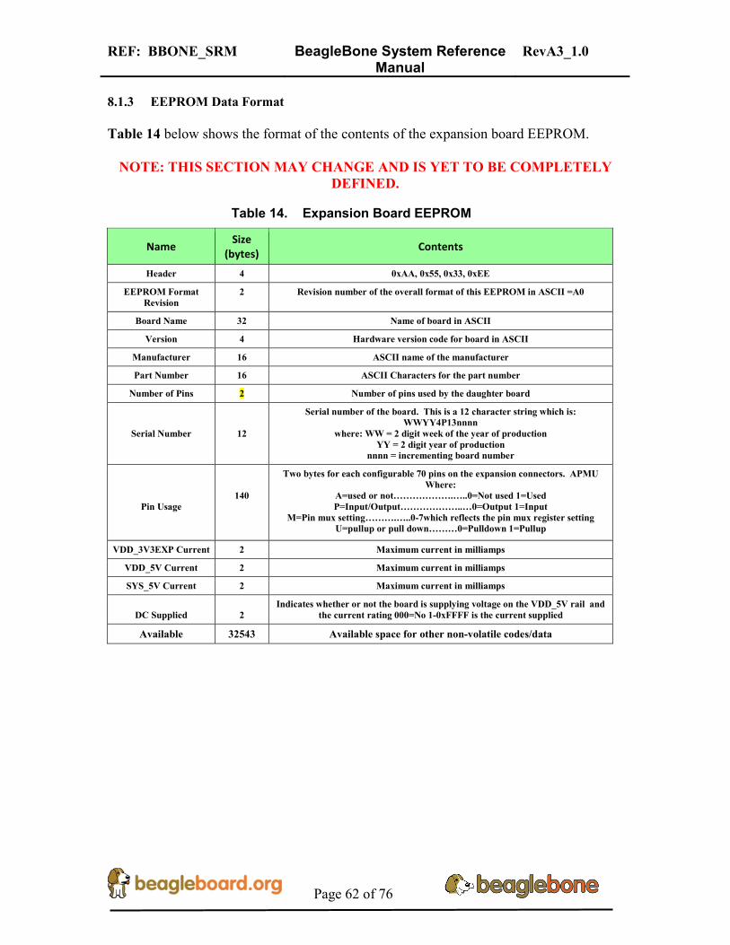
REF: BBONE_SRM BeagleBone System Reference Manual
RevA3_1.0
Page 62 of 76
8.1.3 EEPROM Data Format Table 14 below shows the format of the contents of the expansion board EEPROM.
NOTE: THIS SECTION MAY CHANGE AND IS YET TO BE COMPLETELY DEFINED.
Table 14. Expansion Board EEPROM
Name Size
(bytes) Contents
Header 4 0xAA, 0x55, 0x33, 0xEE
EEPROM Format Revision
2 Revision number of the overall format of this EEPROM in ASCII =A0
Board Name 32 Name of board in ASCII
Version 4 Hardware version code for board in ASCII
Manufacturer 16 ASCII name of the manufacturer
Part Number 16 ASCII Characters for the part number
Number of Pins 2 Number of pins used by the daughter board
Serial Number
12
Serial number of the board. This is a 12 character string which is: WWYY4P13nnnn
where: WW = 2 digit week of the year of production YY = 2 digit year of production
nnnn = incrementing board number
Pin Usage
140
Two bytes for each configurable 70 pins on the expansion connectors. APMU Where:
A=used or not……………….…..0=Not used 1=Used P=Input/Output………………..…0=Output 1=Input
M=Pin mux setting……….…..0-7which reflects the pin mux register setting U=pullup or pull down………0=Pulldown 1=Pullup
VDD_3V3EXP Current 2 Maximum current in milliamps
VDD_5V Current 2 Maximum current in milliamps
SYS_5V Current 2 Maximum current in milliamps
DC Supplied
2
Indicates whether or not the board is supplying voltage on the VDD_5V rail and the current rating 000=No 1-0xFFFF is the current supplied
Available 32543 Available space for other non-volatile codes/data

REF: BBONE_SRM BeagleBone System Reference Manual
RevA3_1.0
Page 63 of 76
8.1.4 Pin Usage Table 15 is the locations in the EEPROM to set the I/O pin usage for the Cape. The table is left blank as a convenience and can be printed out and used as a template for creating custom settings for each cape. A is an indicator and should be a 1 if the pin is used or 0 if it is not used. P indicates if it is an input (1) or output (0). Bits 13-7 are equal to the pin mux setting. U is to set whether a pullup (1) or pulldown (0) is needed on the pin. The unused bits are all zeros. The AIN0-6 pins do not have a pin mux setting, but they need to be set to indicate if each of the pins are used on the Cape.
Table 15. EEPROM Pin Usage
15 14 13 12 11 10 9 8 7 6 5 4 3 2 1 0
LOC Conn Name A P Pin MUX Setting U All 0
89 P9-22 UART2_RXD
90 P9-21 UART2_TXD
91 P9-18 I2C1_SDA
92 P9-17 I2C1_SCL
93 P8-42 GPIO0_7
94 P8-35 UART4_CTSN
95 P8-33 UART4_RTSN
96 P8-31 UART5_CTSN
97 P8-32 UART5_RTSN
98 P9-19 I2C2_SCL
99 P9-20 I2C2_SDA
100 P9-26 UART1_RXD
101 P9-24 UART1_TXD
102 P8-41 CLKOUT2
103 P8-19 EHRPWM2A
104 P8-17 GPIO0_27
105 P9-11 UART4_RXD
106 P9-13 UART4_TXD
107 P8-25 GPIO1_0

REF: BBONE_SRM BeagleBone System Reference Manual
RevA3_1.0
Page 64 of 76
108 P8-24 GPIO1_1
109 P8-5 GPIO1_2
110 P8-6 GPIO1_3
111 P8-23 GPIO1_4
112 P8-22 GPIO1_5
113 P8-3 GPIO1_6
114 P8-4 GPIO1_7
115 P8-12 GPIO1_12
116 P8-11 GPIO1_13
117 P8-16 GPIO1_14
118 P8-15 GPIO1_15
119 P9-15 GPIO1_16
120 P9-23 GPIO1_17
121 P9-14 EHRPWM1A
122 P9-16 EHRPWM1B
123 P9-12 GPIO1_28
124 P8-26 GPIO1_29
125 P8-21 GPIO1_30
126 P8-20 GPIO1_31
127 P8-7 TIMER4
128 P8-9 TIMER5
129 P8-10 TIMER6
130 P8-8 TIMER7
131 P8-45 GPIO2_6
132 P8-46 GPIO2_7
133 P8-43 GPIO2_8
135 P8-44 GPIO2_9
136 P8-41 GPIO2_10
137 P8-42 GPIO2_11
138 P8-39 GPIO2_12
139 P8-40 GPIO2_13
140 P8-37 UART5_TXD
141 P8-38 UART5_RXD
142 P8-36 UART3_CTSN
143 P8-34 UART3_RTSN
144 P8-27 GPIO2_22
145 P8-28 GPIO2_24
146 P8-29 GPIO2_23
147 P8-30 GPIO2_25
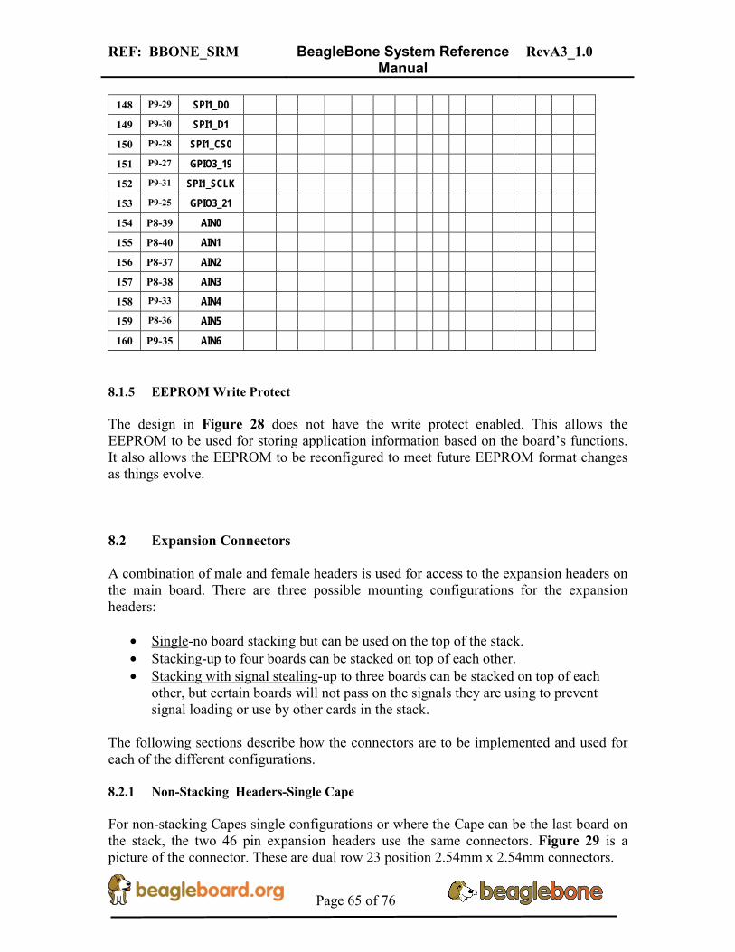
REF: BBONE_SRM BeagleBone System Reference Manual
RevA3_1.0
Page 65 of 76
148 P9-29 SPI1_D0
149 P9-30 SPI1_D1
150 P9-28 SPI1_CS0
151 P9-27 GPIO3_19
152 P9-31 SPI1_SCLK
153 P9-25 GPIO3_21
154 P8-39 AIN0
155 P8-40 AIN1
156 P8-37 AIN2
157 P8-38 AIN3
158 P9-33 AIN4
159 P8-36 AIN5
160 P9-35 AIN6
8.1.5 EEPROM Write Protect The design in Figure 28 does not have the write protect enabled. This allows the EEPROM to be used for storing application information based on the board’s functions. It also allows the EEPROM to be reconfigured to meet future EEPROM format changes as things evolve. 8.2 Expansion Connectors A combination of male and female headers is used for access to the expansion headers on the main board. There are three possible mounting configurations for the expansion headers:
• Single-no board stacking but can be used on the top of the stack. • Stacking-up to four boards can be stacked on top of each other. • Stacking with signal stealing-up to three boards can be stacked on top of each
other, but certain boards will not pass on the signals they are using to prevent signal loading or use by other cards in the stack.
The following sections describe how the connectors are to be implemented and used for each of the different configurations. 8.2.1 Non-Stacking Headers-Single Cape For non-stacking Capes single configurations or where the Cape can be the last board on the stack, the two 46 pin expansion headers use the same connectors. Figure 29 is a picture of the connector. These are dual row 23 position 2.54mm x 2.54mm connectors.

REF: BBONE_SRM BeagleBone System Reference Manual
RevA3_1.0
Page 66 of 76
Figure 29. Single Expansion Connector
The connector is typically mounted on the bottom side of the board as shown in Figure 30. These are very common connectors and should be easily located. You can also use two single row 23 pin headers for each of the dual row headers.
Figure 30. Single Cape Expansion Connector
It is allowed to only populate the pins you need. As this is a non-stacking configuration, there is no need for all headers to be populated. This can also reduce the overall cost of the Cape. This decision is up to the Cape designer. For convenience listed in Table 16 are some possible choices for part numbers on this connector. They have varying pin lengths and some may be more suitable than others for your use. It should be noted, that the longer the pin and the further it is inserted into the BeagleBone connector, the harder it will be to remove due to the tension on 92 pins. This can be minimized by using shorter pins or removing those pins that are not used by your particular design. The minimum the pin length can be is .125(3.175mm) in order to insure connection to the pins in the connector on the BeagleBone.
Table 16. Single Cape Connectors SUPPLIER PARTNUMBER TAIL LENGTH(in) TAIL LENGTH(mm)
Major League TSHC-123-D-03-145-GT-LF .145 3.68 Major League TSHC-123-D-03-240-GT-LF .240 6.10 Major League TSHC-123-D-03-255-GT-LF .255 6.47 The GT in the part number is a plating option. Other options may be used as well as long as the contact area is gold. Other possible sources are Sullins and Samtec for these connectors.
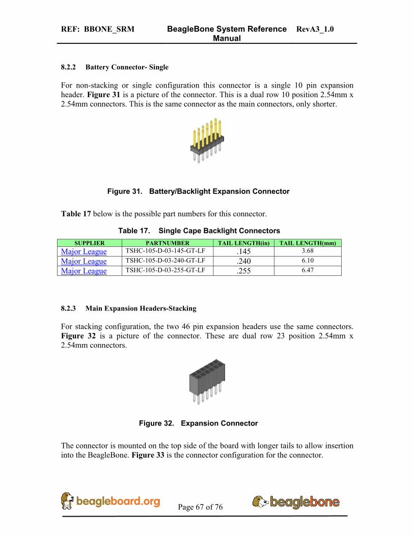
REF: BBONE_SRM BeagleBone System Reference Manual
RevA3_1.0
Page 67 of 76
8.2.2 Battery Connector- Single For non-stacking or single configuration this connector is a single 10 pin expansion header. Figure 31 is a picture of the connector. This is a dual row 10 position 2.54mm x 2.54mm connectors. This is the same connector as the main connectors, only shorter.
Figure 31. Battery/Backlight Expansion Connector
Table 17 below is the possible part numbers for this connector.
Table 17. Single Cape Backlight Connectors SUPPLIER PARTNUMBER TAIL LENGTH(in) TAIL LENGTH(mm)
Major League TSHC-105-D-03-145-GT-LF .145 3.68 Major League TSHC-105-D-03-240-GT-LF .240 6.10 Major League TSHC-105-D-03-255-GT-LF .255 6.47 8.2.3 Main Expansion Headers-Stacking For stacking configuration, the two 46 pin expansion headers use the same connectors. Figure 32 is a picture of the connector. These are dual row 23 position 2.54mm x 2.54mm connectors.
Figure 32. Expansion Connector
The connector is mounted on the top side of the board with longer tails to allow insertion into the BeagleBone. Figure 33 is the connector configuration for the connector.

REF: BBONE_SRM BeagleBone System Reference Manual
RevA3_1.0
Page 68 of 76
Figure 33. Stacked Cape Expansion Connector
For convenience listed in Table 18 are some possible choices for part numbers on this connector. They have varying pin lengths and some may be more suitable than others for your use. It should be noted, that the longer the pin and the further it is inserted into the BeagleBone connector, the harder it will be to remove due to the tension on 92 pins. This can be minimized by using shorter pins. There are most likely other suppliers out there that will work for this connector as well. If anyone finds other suppliers of compatible connectors that work, let us know and they will be added to this document. The minimum length of the pin that inserts into the BeagleBone connector is .125 (3.175mm).
Table 18. Stacked Cape Connectors SUPPLIER PARTNUMBER TAIL LENGTH(in) TAIL LENGTH(mm)
Major League SSHQ-123-D-06-GT-LF .190 4.83 Major League SSHQ-123-D-08-GT-LF .390 9.91 Major League SSHQ-123-D-10-GT-LF .560 14.22
There are also different plating options on each of the connectors above. Gold plating on the contacts is the minimum requirement. If you choose to use a different part number for plating or availability purposes, make sure you do not select the “LT” option. Other possible sources are Sullins and Samtec. 8.2.4 Battery Connector Stacking This connector is a single two 10 pin expansion header. Figure 34 is a picture of the connector. This is a dual row 10 position 2.54mm x 2.54mm connector and is the same as the main connector except with less positions.
Figure 34. Stacked Battery Expansion Connector
For convenience listed in Table 19 are some possible choices for part numbers on this connector. They have varying pin lengths and some may be more suitable than others for your use.

REF: BBONE_SRM BeagleBone System Reference Manual
RevA3_1.0
Page 69 of 76
Table 19. Stacked Cape Connectors SUPPLIER PARTNUMBER TAIL LENGTH(in) TAIL LENGTH(mm)
Major League SSHQ-105-D-06-GT-LF .190 4.83 Major League SSHQ-105-D-08-GT-LF .390 9.91 Major League SSHQ-105-D-10-GT-LF .560 14.22
Tail length does not include the thickness of the Cape PCB. 8.2.5 Stacked Capes w/Signal Stealing Figure 35 is the connector configuration for stackable Capes that does not provide all of the signals upwards for use by other boards. This is useful if there is an expectation that other boards could interfere with the operation of your board by exposing those signals for expansion. This configuration consists of a combination of the stacking and non-stacking style connectors.
Figure 35. Stacked w/Signal Stealing Expansion Connector
8.3 Signal Usage Based on the pin muxing capabilities of the processor, each expansion pin can be configured for different functions. When in the stacking mode, it will be up to the user to insure that any conflicts are resolved between multiple stacked cards. When stacked, the first card detected will be used to set the pin muxing of each pin. This will prevent other modes from being supported on stacked cards and may result in them being inoperative. In Section 7.12 of this document, the functions of the pins are defined as well as the pin muxing options. Refer to this section for more information on what each pin is. To simplify things, if you use the default name as the function for each pin and use those functions, it will simplify board design and reduce conflicts with other boards. Interoperability is up to the board suppliers and the user. This specification does not specify a fixed function on any pin and any pin can be used to the full extent of the functionality of that pin as enabled by the processor. 8.4 Cape Power

REF: BBONE_SRM BeagleBone System Reference Manual
RevA3_1.0
Page 70 of 76
This section describes the power rails for the Capes and their usage. 8.4.1 Main Board Power The Table 20 describes the voltages from the main board that are available on the expansion connectors and their ratings. All voltages are supplied by connector P9. The current ratings listed are per pin.
Table 20. Expansion Voltages
Current Name P9 Name Current GND 1 2 GND
250mA VDD_3V3EXP 3 4 VDD_3V3EXP 250mA
1000mA VDD_5V 5 6 VDD_5V 1000mA
250mA SYS_5V 7 8 SYS_5V 250mA
: : GND 43 44 GND
GND 45 46 GND The VDD_3V3EXP rail is supplied by the LDO on the BeagleBone and is the primary power rail for expansion boards. VDD_5V is the main power supply from the DC input jack. This voltage is not present when the board is powered via USB. The amount of current supplied by this rail is dependent upon the amount of current available. Based on the board design, this rail is limited to 1A per pin from the main board. The SYS_5V rail is the main rail for the regulators on the main board. When powered from a DC supply or USB, this rail will be 5V. The available current from this rail depends on the current available from the USB and DC external supplies. 8.4.2 Expansion Board External Power A Cape can have a jack or terminals to bring in whatever voltages may be needed by that board. Care should be taken not to let this voltage feedback into any of the expansion header pins. It is possible to provide 5V to the main board from an expansion board. By supplying a 5V signal into the VDD_5V rail, the main board can be supplied. This voltage must not exceed 5V. You should not supply any voltage into any other pin of the expansion connectors. Based on the board design, this rail is limited to 1A per pin to the BeagleBone.

REF: BBONE_SRM BeagleBone System Reference Manual
RevA3_1.0
Page 71 of 76
8.4.3 Mechanical This section provides the guidelines for the creation of expansion boards from a mechanical standpoint. Defined is a standard board size that is the same profile as the BeagleBone. It is expected that the majority of expansion boards created will be of standard size. It is possible to create boards of other sizes and in some cases this is required, as in the case of an LCD larger than the BeagleBone board. 8.4.4 Standard Cape Size Figure 36 is the outline of the standard Cape. The dimensions are in inches.
Figure 36. Cape Board Dimensions
A slot is provided for the Ethernet connector to stick up higher than the Cape when mounted. This also acts as a key function to insure that the Cape is oriented correctly. Space is also provided to allow access to the user LEDs and reset button on the main board. 8.4.5 Extended Cape Size Capes larger than the standard board size are also allowed. A good example would be an LCD panel. There is no practical limit to the sizes of these types of boards. The notch for

REF: BBONE_SRM BeagleBone System Reference Manual
RevA3_1.0
Page 72 of 76
the key is also not required, but it is up to the supplier of these boards to insure that the BeagleBone is not plugged in incorrectly in such a manner that damage would be cause to the BeagleBone or any other Capes that may be installed. Any such damage will be the responsibility of the supplier of such a Cape to repair. As with all Capes, the EEPROM is required and compliance with the power requirements must be adhered to.
9.0 Board Setup This section describes how to setup the board and to make sure that it is operating. It also provides an advanced section that allows you to run a self diagnostic test that does require additional equipment to be purchased. 9.1 USB Powered Setup The board ships with everything you need for this configuration.
• BeagleBone • microSD card with bootable SW • USB Type A to 5 pin connector
To setup the board:
1) Insert the SD card into the SD card connector 2) Plug the USB cable into the BeagleBone 3) Plug the other end of the USB cable into the PC USB port. 4) The power LED D1 should be on 5) After a few seconds, USER0 and USER1 LED should start flashing 6) After 10 seconds or so, the board should show up as a mass storage device on
your PC 7) Open the new drive and click on the Readme.html file. 8) The file should open in your browser. 9) Follow the instructions on the HTML page.
9.2 DC Powered Setup The board ships with everything you need for this configuration except for a power supply. The first three items below are provided and the power supply will need to be provided by you.
• BeagleBone • microSD card with bootable SW • USB Type A to 5 pin connector • 5VDC 1A power supply w/2.1mm x 5.5mm connector, center positive.

REF: BBONE_SRM BeagleBone System Reference Manual
RevA3_1.0
Page 73 of 76
To setup the board:
1) Insert the SD card into the SD card connector 2) Plug the DC cable into the board. 3) The power LED D1 should be on 4) Plug the USB cable into the BeagleBone 5) Plug the other end of the USB cable into the PC USB port. 6) After a few seconds, USER0 and USER1 LED should start flashing 7) After 10 seconds or so, the board should show up as a mass storage device on
your PC 8) Open the new drive and click on the Readme.html file. 9) The file should open in your browser. 10) Follow the instructions on the HTML page.
9.3 Advanced Test This test involves the purchase of a USB hub that is equipped with an Ethernet port or the use of a USB Hub with a USB to Ethernet Dongle plugged in. The SW that ships with the board is capable of running this test. You may need to load drivers for your particular Hub or Ethernet dongle. The following procedure will setup and test the board. The following items are tested on the board:
• USB Client Port • USB Host Port • Ethernet Port • DDR • PMIC • EEPROM • Processor • SD Slot • DC Power • USB HUB • USB to Serial • LEDs
9.3.1 Equipment Needed The following items are needed to perform this test:
1) USB Hub with Ethernet port 2) Ethernet Cable

REF: BBONE_SRM BeagleBone System Reference Manual
RevA3_1.0
Page 74 of 76
3) USB A Male to 5pin male 4) BeagleBone 5) 26 AWG jumper wire, stripped 6) 5VDC 1A power supply, 2.1mm Center positive
9.3.2 Procedure
1) Connect the USB HUB to the USB Host port of the BeagleBone. 2) Connect the HUB Ethernet port to the BeagleBone Ethernet port. 3) Connect one of the USB ports to USB connector on the BeagleBone. 4) Insert the SD card that came with the board into the SD connector. 5) Add a jumper wire between pin 2 and 3 of the P8. This tells the SW to run the
test. 6) Insert the DC power supply 7) The PWR LED should turn on. 8) Then D2 and D3 should start flashing indicating the boot process has begun. 9) After about a minute, D2 and D3 should turn off and D5 should start flashing. 10) D5 will continue to flash during the test process which should take about 2-3
minutes. 11) At the end of the test one of two things will happen:
a. If all the LEDS are on solid, then the board has passed the test. b. If all LEDS are flashing, then the board has failed the test.
9.3.3 Debugging It is possible to add a USB to serial cable to the HUB for messages as the tests run. This will tell you where the test fails. It will require a USB to serial adapter to also be plugged into your PC and a Null modem female to female adapter be placed between the two cables. In order for this to work, the Linux driver needs to be installed on the BeagleBone for the USB to serial adapter. For now, only one USB to serial adapter is supported. Others will be added over time. Once you have the correct cable configuration, you can open up a terminal program set to the serial port and set for 115KBaud, 8,n2 and no handshaking. The results of the test as run will be printed to the terminal.

REF: BBONE_SRM BeagleBone System Reference Manual
RevA3_1.0
Page 75 of 76
10.0 BeagleBone Mechanical Specification
Size: 3.5” x 2.1” (86.36mm x 53.34mm) Max height: .187” (4.76mm) PCB Layers: 6 PCB thickness: .062”
RoHS Compliant: Yes Weight: TBW
Figure 37. Board Top Profile
Figure 38. Board Bottom Profile

REF: BBONE_SRM BeagleBone System Reference Manual
RevA3_1.0
Page 76 of 76
11.0 Design Information Design information can be found on the SD card that ships with board under the documents/hardware directory when connected over the USB cable. Provided there is:
• Schematic in PDF • Schematic in OrCAD • PCB Gerber • PCB Layout File • Bill of Material • System Reference Manual (This document).
You can also download the files from http://beagleboard.org/hardware/design . ALL support for this design is through the BeagleBoard.org community. There are also some community members working to convert the schematics and PCB files into other formats. Look for those to available in the future.