b.e - iv semester · arm alp 9. arm using keil 10. bcd up-down counter 11. 7 – segment display 12...
TRANSCRIPT
Channabasaveshwara Institute of Technology (Affiliated to VTU, Belgaum & Approved by AICTE, New Delhi)
(NAAC Accredited & ISO 9001:2015 Certified Institution)
NH 206 (B.H. Road), Gubbi, Tumkur – 572 216. Karnataka.
Department of Information Science & Engineering
Microprocessors and Microcontrollers Laboratory
Subject Code: 17CSL48
B.E - IV Semester
Lab Manual 2018-19
Channabasaveshwara Institute of Technology (Affiliated to VTU, Belgaum & Approved by AICTE, New Delhi)
(NAAC Accredited & ISO 9001:2015 Certified Institution)
NH 206 (B.H. Road), Gubbi, Tumkur – 572 216. Karnataka.
Department of Information Science and Engineering
BE – IV Semester
MICROPROCESSOR AND MICROCONTROLLER
LABORATORY
[As per Choice Based Credit System (CBCS) scheme]
17CSL48
Academic Year : 2018-19
Prepared By:
BASAVESH D
Asst. Professor
Dept. of ISE
CIT. Gubbi
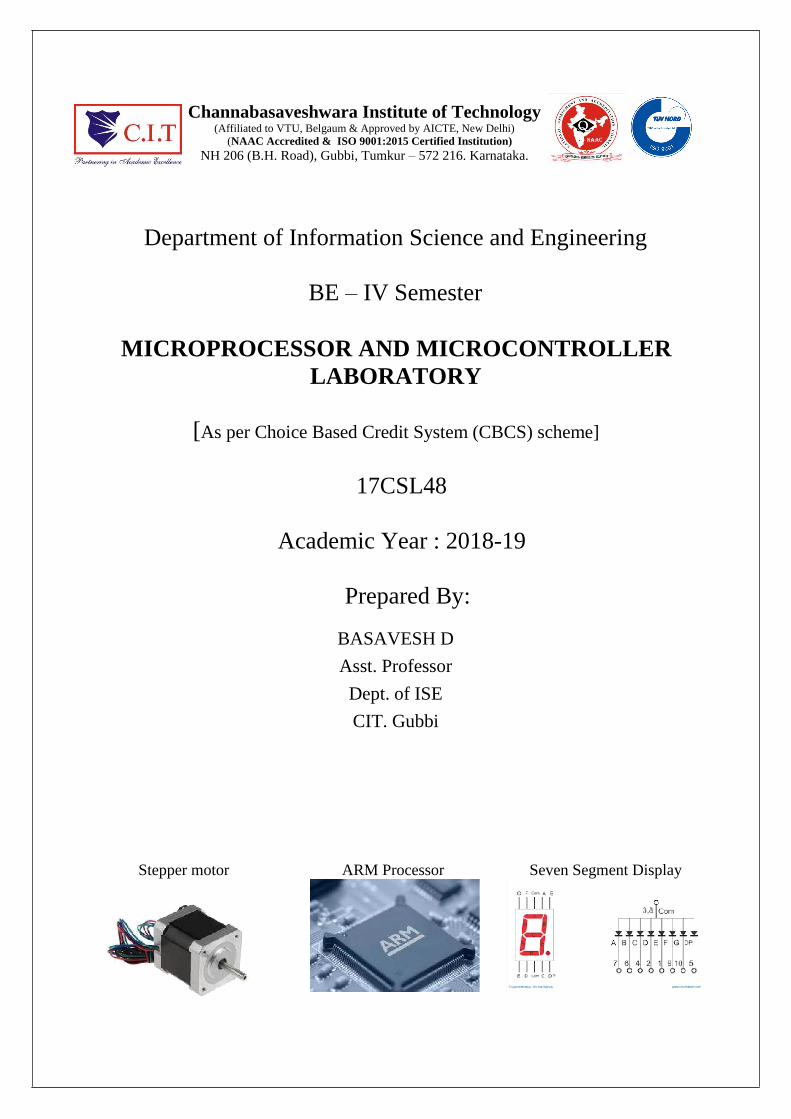
Stepper motor ARM Processor Seven Segment Display
Channabasaveshwara Institute of Technology (Affiliated to VTU, Belgaum & Approved by AICTE, New Delhi)
(NAAC Accredited & ISO 9001:2015 Certified Institution)
NH 206 (B.H. Road), Gubbi, Tumkur – 572 216. Karnataka.
Department of Information Science and Engineering
BE – IV Semester
MICROPROCESSOR AND MICROCONTROLLER
LABORATORY
[As per Choice Based Credit System (CBCS) scheme]
17CSL48
Academic Year : 2018-19
NAME: ____________________________________
USN: ______________________________________
BATCH: ___________ Section: _________________

QMP 7.1 D/F
Channabasaveshwara Institute of Technology
(An ISO 9001:2008 Certified Institution)
NH 206 (B.H. Road), Gubbi, Tumkur – 572 216. Karnataka.
SYLLABUS
Laboratory Code: 17CSL48 IA Marks 20
Number of Lecture Hours/Week 01I + 02P Exam Marks 80
Total Number of Lecture Hours 40 Exam Hours 03
CREDITS: 02
Course objectives: This course will enable students to
To provide practical exposure to the students on microprocessors, design and coding knowledge on 80x86 family/ARM.
To give the knowledge and practical exposure on connectivity and execute of interfacing
devices with 8086/ARM kit like LED displays, Keyboards, DAC/ADC, and various other devices.
Description: Demonstration and Explanation hardware components and Faculty in-charge should explain 8086 architecture, pin diagram in one slot. The second slot, the Faculty in-charge should explain instruction set types/category etc. Students have to prepare a write-up on the same and include it in the Lab record and to be evaluated.
Laboratory Session-1: Write-up on Microprocessors, 8086 Functional block diagram, Pin diagram and description. The same information is also taught in theory class; this helps the students to understand better.
Laboratory Session-2: Write-up on Instruction group, Timing diagrams, etc. The same information is also taught in theory class; this helps the students to understand better.
Note: These TWO Laboratory sessions are used to fill the gap between theory classes and
practical sessions. Both sessions are evaluated as lab experiments for 20 marks.
Experiments: • Develop and execute the following programs using 8086 Assembly Language. Any suitable assembler like MASM/TASM/8086 kit or any equivalent software may be used. • Program should have suitable comments. • The board layout and the circuit diagram of the interface are to be provided to the student during the examination. • Software Required: Open source ARM Development platform, KEIL IDE and Proteus for simulation
SOFTWARE PROGRAMS : PART A
1. Design and develop an assembly language program to search a key element “X” in a list
of „n‟ 16-bit numbers. Adopt Binary search algorithm in your program for searching. 2. Design and develop an assembly program to sort a given set of „n‟ 16-bit numbers
in ascending order. Adopt Bubble Sort algorithm to sort given elements. 3. Develop an assembly language program to reverse a given string and verify whether it is a
palindrome or not. Display the appropriate message. 4. Develop an assembly language program to compute nCr using recursive procedure. Assume
that „n‟ and „r‟ are non-negative integers. 5. Design and develop an assembly language program to read the current time and Date
from the system and display it in the standard format on the screen. 6. To write and simulate ARM assembly language programs for data transfer, arithmetic
and logical operations (Demonstrate with the help of a suitable program). 7. . To write and simulate C Programs for ARM microprocessor using KEIL (Demonstrate with
the help of a suitable program)
Note : To use KEIL one may refer the book: Insider’s Guide to the ARM7 based microcontrollers, Hitex Ltd.,1st edition, 2005
HARDWARE PROGRAMS : PART B
8. a. Design and develop an assembly program to demonstrate BCD Up-Down Counter (00-99)
on the Logic Controller Interface. b. Design and develop an assembly program to read the status of two 8-bit inputs (X & Y) from the Logic Controller Interface and display X*Y.
9. Design and develop an assembly program to display messages “FIRE” and “HELP” alternately with flickering effects on a 7-segment display interface for a suitable period of time. Ensure a flashing rate that makes it easy to read both the messages (Examiner does not specify these delay values nor is it necessary for the student to compute these values).
10. Design and develop an assembly program to drive a Stepper Motor interface and rotate the motor in specified direction (clockwise or counter-clockwise) by N steps (Direction and N are specified by the examiner). Introduce suitable delay between successive steps. (Any arbitrary value for the delay may be assumed by the student).
11. . Design and develop an assembly language program to a. Generate the Sine Wave using DAC interface (The output of the DAC is to be displayed on the CRO). b. Generate a Half Rectified Sine waveform using the DAC interface. (The output of the DAC is to be displayed on the CRO).
12. To interface LCD with ARM processor-- ARM7TDMI/LPC2148. Write and execute programs in C language for displaying text messages and numbers on LCD
13. To interface Stepper motor with ARM processor-- ARM7TDMI/LPC2148. Write a program to rotate stepper motor
STUDY EXPERIMENTS: 1. Interfacing of temperature sensor with ARM freedom board (or any other ARM
microprocessor board) and display temperature on LCD 2. To design ARM cortex based automatic number plate recognition system
3. To design ARM based power saving system
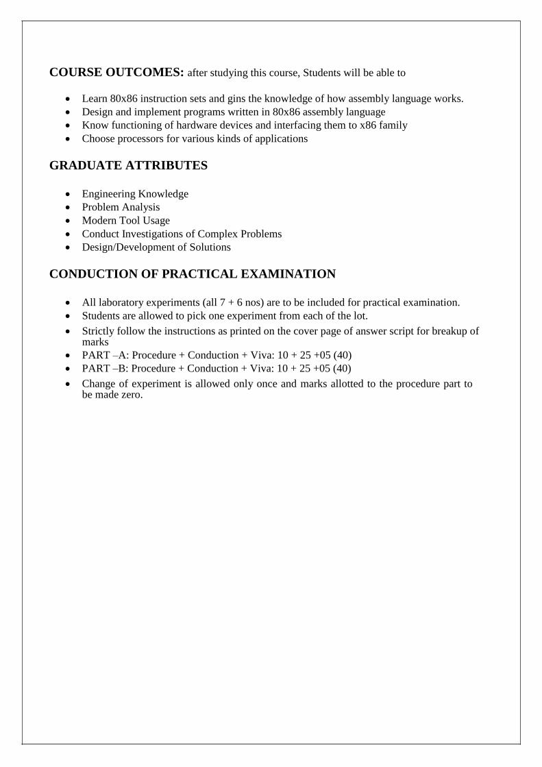
COURSE OUTCOMES: after studying this course, Students will be able to
Learn 80x86 instruction sets and gins the knowledge of how assembly language works.
Design and implement programs written in 80x86 assembly language
Know functioning of hardware devices and interfacing them to x86 family Choose processors for various kinds of applications
GRADUATE ATTRIBUTES
Engineering Knowledge
Problem Analysis
Modern Tool Usage Conduct Investigations of Complex Problems
Design/Development of Solutions
CONDUCTION OF PRACTICAL EXAMINATION
All laboratory experiments (all 7 + 6 nos) are to be included for practical examination.
Students are allowed to pick one experiment from each of the lot.
Strictly follow the instructions as printed on the cover page of answer script for breakup of marks
PART –A: Procedure + Conduction + Viva: 10 + 25 +05 (40)
PART –B: Procedure + Conduction + Viva: 10 + 25 +05 (40)
Change of experiment is allowed only once and marks allotted to the procedure part to be made zero.
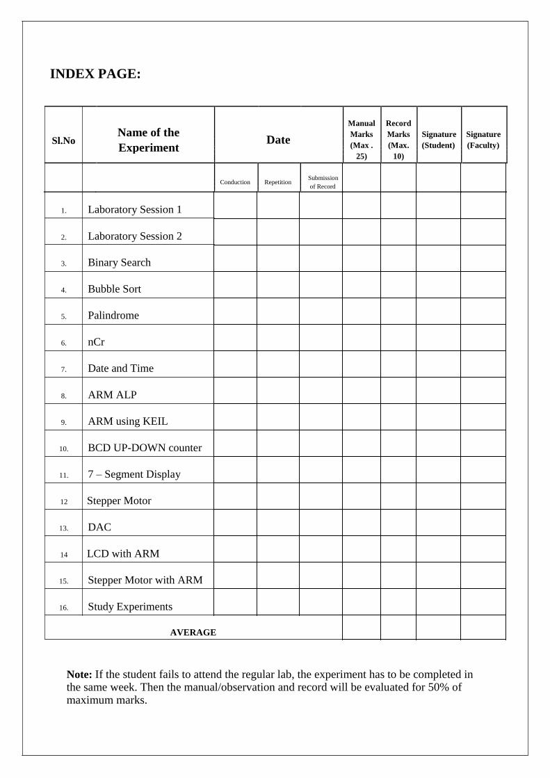
INDEX PAGE:
Name of the
Manual Record
Sl.No
Date Marks Marks Signature Signature
Experiment (Max . (Max. (Student) (Faculty)
25) 10)
Conduction Repetition Submission
of Record
1. Laboratory Session 1
2. Laboratory Session 2
3. Binary Search
4. Bubble Sort
5. Palindrome
6. nCr
7. Date and Time
8. ARM ALP
9. ARM using KEIL
10. BCD UP-DOWN counter
11. 7 – Segment Display
12 Stepper Motor
13. DAC
14 LCD with ARM
15. Stepper Motor with ARM
16. Study Experiments
AVERAGE
Note: If the student fails to attend the regular lab, the experiment has to be completed in
the same week. Then the manual/observation and record will be evaluated for 50% of maximum marks.
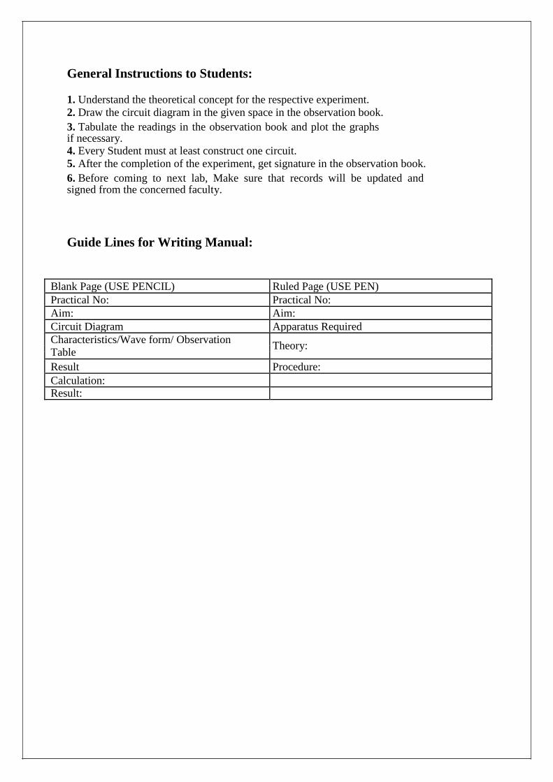
General Instructions to Students:
1. Understand the theoretical concept for the respective experiment.
2. Draw the circuit diagram in the given space in the observation book.
3. Tabulate the readings in the observation book and plot the graphs if necessary. 4. Every Student must at least construct one circuit.
5. After the completion of the experiment, get signature in the observation book.
6. Before coming to next lab, Make sure that records will be updated and signed from the concerned faculty.
Guide Lines for Writing Manual:
Blank Page (USE PENCIL) Ruled Page (USE PEN)
Practical No: Practical No:
Aim: Aim:
Circuit Diagram Apparatus Required
Characteristics/Wave form/ Observation Theory:
Table
Result Procedure:
Calculation:
Result:
QMP 7.1 D/F
Channabasaveshwara Institute of Technology
(An ISO 9001:2008 Certified Institution)
NH 206 (B.H. Road), Gubbi, Tumkur – 572 216. Karnataka.
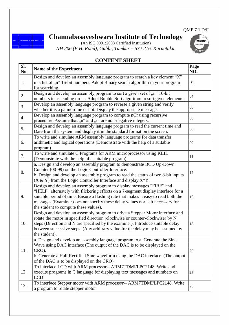
CONTENT SHEET
Sl. Name of the Experiment
Page
No NO.
Design and develop an assembly language program to search a key element “X”
1. in a list of „n‟ 16-bit numbers. Adopt Binary search algorithm in your program 01
for searching.
2.
Design and develop an assembly program to sort a given set of „n‟ 16-bit 04
numbers in ascending order. Adopt Bubble Sort algorithm to sort given elements.
3.
Develop an assembly language program to reverse a given string and verify 05
whether it is a palindrome or not. Display the appropriate message.
4.
Develop an assembly language program to compute nCr using recursive 06
procedure. Assume that „n‟ and „r‟ are non-negative integers.
5.
Design and develop an assembly language program to read the current time and 08
Date from the system and display it in the standard format on the screen.
To write and simulate ARM assembly language programs for data transfer,
6. arithmetic and logical operations (Demonstrate with the help of a suitable 09
program).
7.
To write and simulate C Programs for ARM microprocessor using KEIL 11
(Demonstrate with the help of a suitable program)
a. Design and develop an assembly program to demonstrate BCD Up-Down
8.
Counter (00-99) on the Logic Controller Interface. 12
b. Design and develop an assembly program to read the status of two 8-bit inputs
(X & Y) from the Logic Controller Interface and display X*Y.
Design and develop an assembly program to display messages “FIRE” and
“HELP” alternately with flickering effects on a 7-segment display interface for a
9. suitable period of time. Ensure a flashing rate that makes it easy to read both the 16
messages (Examiner does not specify these delay values nor is it necessary for
the student to compute these values).
Design and develop an assembly program to drive a Stepper Motor interface and
rotate the motor in specified direction (clockwise or counter-clockwise) by N
10. steps (Direction and N are specified by the examiner). Introduce suitable delay 18
between successive steps. (Any arbitrary value for the delay may be assumed by
the student).
a. Design and develop an assembly language program to a. Generate the Sine
Wave using DAC interface (The output of the DAC is to be displayed on the
11. CRO). 20
b. Generate a Half Rectified Sine waveform using the DAC interface. (The output
of the DAC is to be displayed on the CRO).
To interface LCD with ARM processor-- ARM7TDMI/LPC2148. Write and
12. execute programs in C language for displaying text messages and numbers on 23
LCD
13.
To interface Stepper motor with ARM processor-- ARM7TDMI/LPC2148. Write 26
a program to rotate stepper motor

Microprocessors Lab 17CSL48
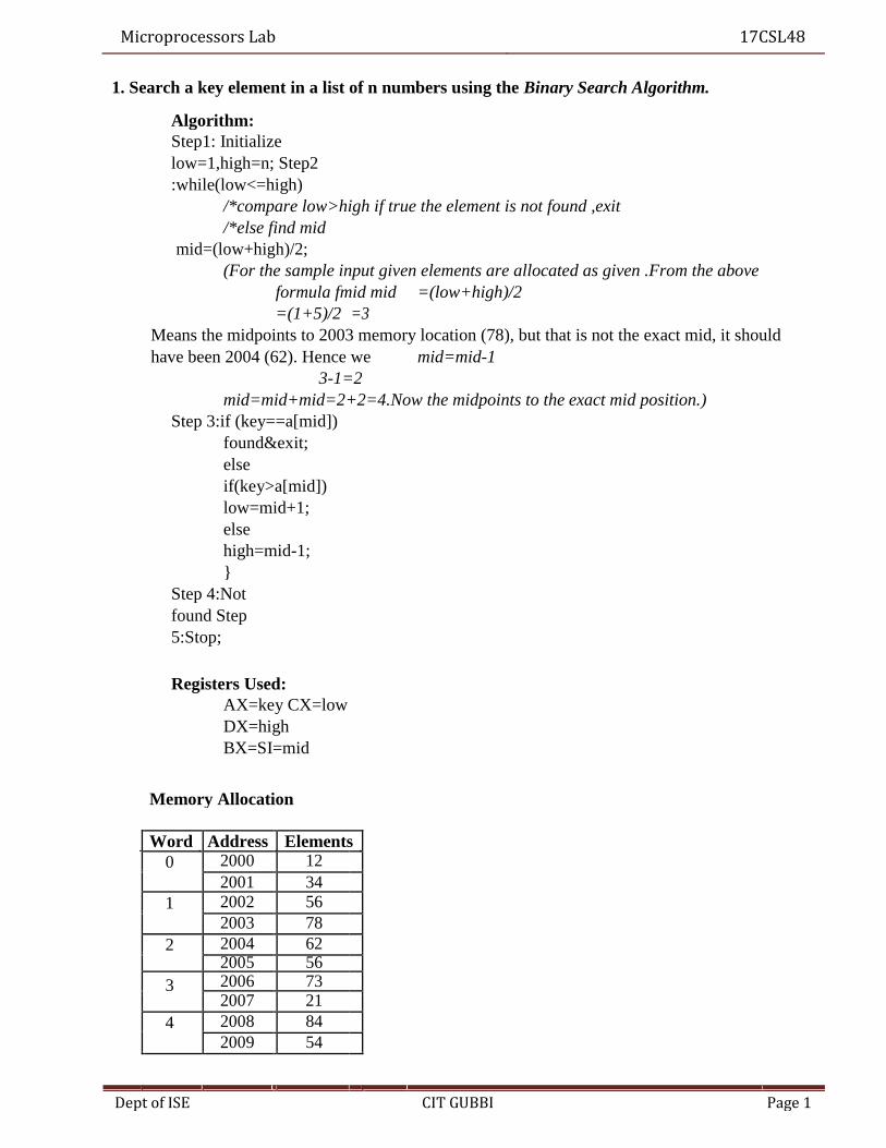
1. Search a key element in a list of n numbers using the Binary Search Algorithm. Algorithm:
Step1: Initialize
low=1,high=n; Step2
:while(low<=high)
/*compare low>high if true the element is not found ,exit
/*else find mid
mid=(low+high)/2;
(For the sample input given elements are allocated as given .From the above
formula fmid mid =(low+high)/2
=(1+5)/2 =3
Means the midpoints to 2003 memory location (78), but that is not the exact mid, it should
have been 2004 (62). Hence we mid=mid-1
3-1=2
mid=mid+mid=2+2=4.Now the midpoints to the exact mid position.)
Step 3:if (key==a[mid])
found&exit;
else
if(key>a[mid])
low=mid+1;
else
high=mid-1;
}
Step 4:Not
found Step
5:Stop;
Registers Used:
AX=key CX=low
DX=high
BX=SI=mid
Memory Allocation
Word Address Elements
0 2000 12
2001 34
1 2002 56
2003 78
2 2004 62
2005 56
3 2006 73
2007
21
4 2008 84
2009 54
Dept of ISE CIT GUBBI Page 1
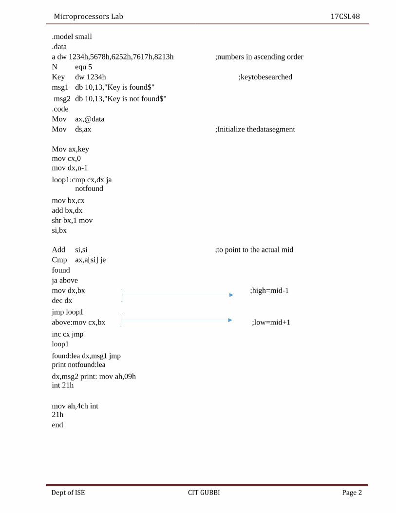
Microprocessors Lab 17CSL48
.model small
.data
a dw 1234h,5678h,6252h,7617h,8213h ;numbers in ascending order
N equ 5
Key dw 1234h ;keytobesearched
msg1 db 10,13,"Key is found$"
msg2 db 10,13,"Key is not found$"
.code
Mov ax,@data
Mov ds,ax ;Initialize thedatasegment
Mov ax,key
mov cx,0
mov dx,n-1
loop1:cmp cx,dx ja notfound
mov bx,cx
add bx,dx
shr bx,1 mov
si,bx
Add si,si ;to point to the actual mid
Cmp ax,a[si] je
found
ja above
mov dx,bx ;high=mid-1
dec dx
jmp loop1
above:mov cx,bx ;low=mid+1
inc cx jmp
loop1
found:lea dx,msg1 jmp
print notfound:lea
dx,msg2 print: mov ah,09h int 21h
mov ah,4ch int 21h end
Dept of ISE CIT GUBBI Page 2

Microprocessors Lab 17CSL48
Output Sample Input:
8213h
F:\MASM> filename.exe
KEYFOUND
Program terminated normally
Sample Input: 5623h
F:\MASM> filename.exe
KEYNOTFOUND
Program terminated normally
Dept of ISE CIT GUBBI Page 3

Microprocessors Lab 17CSL48
2. Sort a given set of ‘n’ numbers in ascending using Bubble-Sort algorithm.
.model small
.data
Arr db 5,1,8,7,4,3 ;array to be sorted
Len equ $-arr ;to find the length of array
.code
Mov ax,@data
Mov ds,ax ; initializing the data segment
mov ch,len-1 ;ch holds number of passes
again:mov cl,ch ;cl holds number of comparisons
mov si,offset arr ;point si to the first element of array
repeat:mov al,[si] inc si
cmp al,[si]
jbe next
xchg al,[si] ;Exchange the content of two locations
mov [si-1],al
next: dec cl
jnz repeat
dec ch
jnz again
int 3 end
Output
F:\MASM>afdebug filename.exe
In the debugging window keep pressing F1 until the given numbers are arranged in the ascending order.
Dept of ISE CIT GUBBI Page 4
Microprocessors Lab 17CSL48
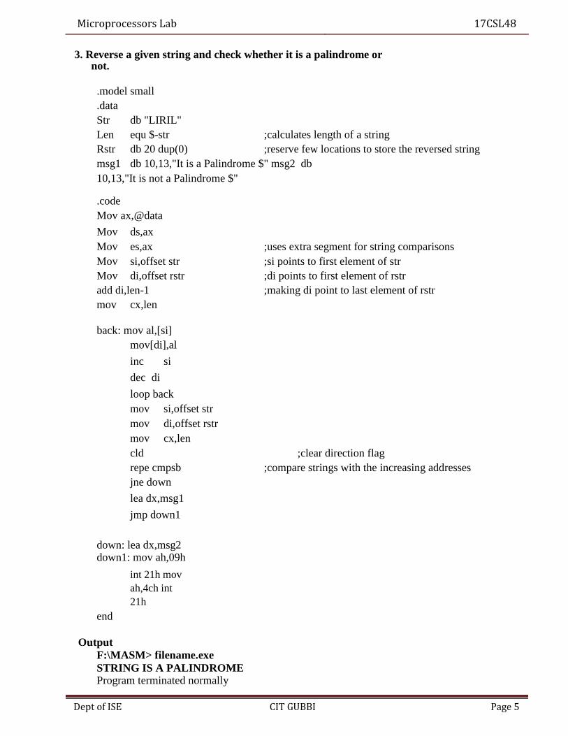
3. Reverse a given string and check whether it is a palindrome or
not.
.model small
.data
Str db "LIRIL"
Len equ $-str ;calculates length of a string
Rstr db 20 dup(0) ;reserve few locations to store the reversed string
msg1 db 10,13,"It is a Palindrome $" msg2 db
10,13,"It is not a Palindrome $"
.code
Mov ax,@data
Mov ds,ax
Mov es,ax ;uses extra segment for string comparisons
Mov si,offset str ;si points to first element of str
Mov di,offset rstr ;di points to first element of rstr
add di,len-1 ;making di point to last element of rstr
mov cx,len
back: mov al,[si]
mov[di],al
inc si
dec di
loop back
mov si,offset str
mov di,offset rstr
mov cx,len
cld ;clear direction flag
repe cmpsb ;compare strings with the increasing addresses
jne down
lea dx,msg1
jmp down1
down: lea dx,msg2 down1: mov ah,09h
int 21h mov
ah,4ch int
21h end
Output
F:\MASM> filename.exe
STRING IS A PALINDROME Program terminated normally
Dept of ISE CIT GUBBI Page 5

Microprocessors Lab 17CSL48
4. Compute nCr using recursive procedure. Assume that ‘n’ and ‘r’ are non-negative integers
To find nCr:
Step 1: if r=0 or n=r then nCr=1 Step 2: if r =1 or r = n-1 then nCr=n Step 3: Recursive definition of nCr is
nCr = (n-1) C r + (n-1)C(r-1)
.model small
.data
N dw 8 R dw 2 Res dw 0
.code
Mov ax,@data
Mov ds,ax
Mov ax,n
Mov bx,r
Call ncr
mov ah,4ch int 21h
ncr proc cmp bx,0 je res1 cmp bx,ax je res1 cmp bx,01h je res2 dec ax cmp ax,bx je incrn push ax
push bx
callncr pop bx pop ax dec bx push ax push bx
Dept of ISE CIT GUBBI Page 6

Microprocessors Lab 17CSL48
call ncr
pop bx pop ax ret
res1:inc res ret incrn:inc ax res2:add res,ax ret ncr endp
Output
F:\MASM>afdebug filename.exe
In the debugging window keep pressing F1 until you get the result, i.e., the value of ncr
Dept of ISE CIT GUBBI Page 7
Microprocessors Lab 17CSL48
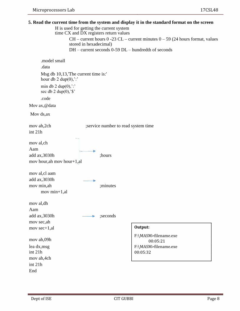
5. Read the current time from the system and display it in the standard format on the screen
H is used for getting the current system time CX and DX registers return values
CH – current hours 0 -23 CL – current minutes 0 – 59 (24 hours format, values stored in hexadecimal) DH – current seconds 0-59 DL – hundredth of seconds
.model small
.data
Msg db 10,13,'The current time is:' hour db 2 dup(0),‟:‟
min db 2 dup(0),‟:‟
sec db 2 dup(0),‟$‟
.code
Mov ax,@data Mov ds,ax
mov ah,2ch ;service number to read system time
int 21h
mov al,ch
Aam
add ax,3030h ;hours
mov hour,ah mov hour+1,al
mov al,cl aam
add ax,3030h
mov min,ah ;minutes
mov min+1,al
mov al,dh
Aam
add ax,3030h ;seconds
mov sec,ah
Output:
mov sec+1,al
mov ah,09h F:\MASM>filename.exe
00:05:21
lea dx,msg F:\MASM>filename.exe
int 21h 00:05:32
mov ah,4ch
int 21h
End
Dept of ISE CIT GUBBI Page 8
Microprocessors Lab 17CSL48
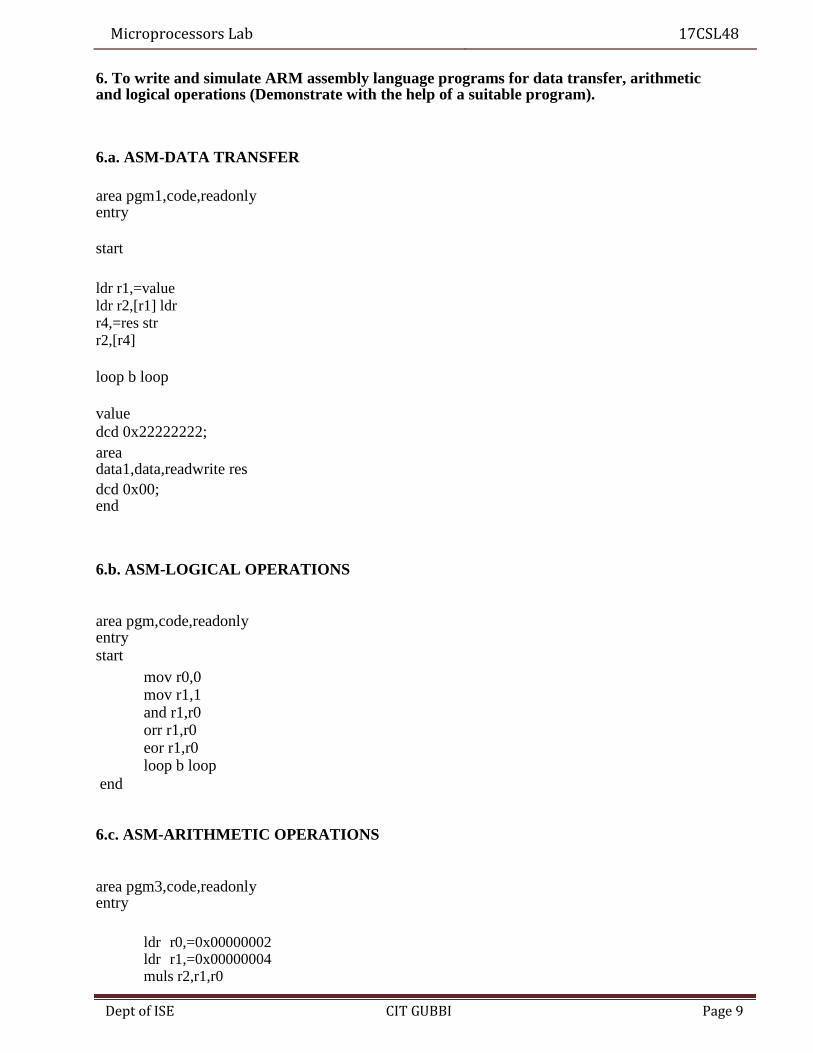
6. To write and simulate ARM assembly language programs for data transfer, arithmetic and logical operations (Demonstrate with the help of a suitable program).
6.a. ASM-DATA TRANSFER
area pgm1,code,readonly entry
start
ldr r1,=value ldr r2,[r1] ldr r4,=res str r2,[r4]
loop b loop
value
dcd 0x22222222; area data1,data,readwrite res dcd 0x00; end
6.b. ASM-LOGICAL OPERATIONS
area pgm,code,readonly entry start
mov r0,0 mov r1,1 and r1,r0 orr r1,r0 eor r1,r0 loop b loop
end
6.c. ASM-ARITHMETIC OPERATIONS
area pgm3,code,readonly entry
ldr r0,=0x00000002 ldr r1,=0x00000004 muls r2,r1,r0
Dept of ISE CIT GUBBI Page 9

Microprocessors Lab 17CSL48
loop b loop end
Dept of ISE CIT GUBBI Page 10
Microprocessors Lab 17CSL48
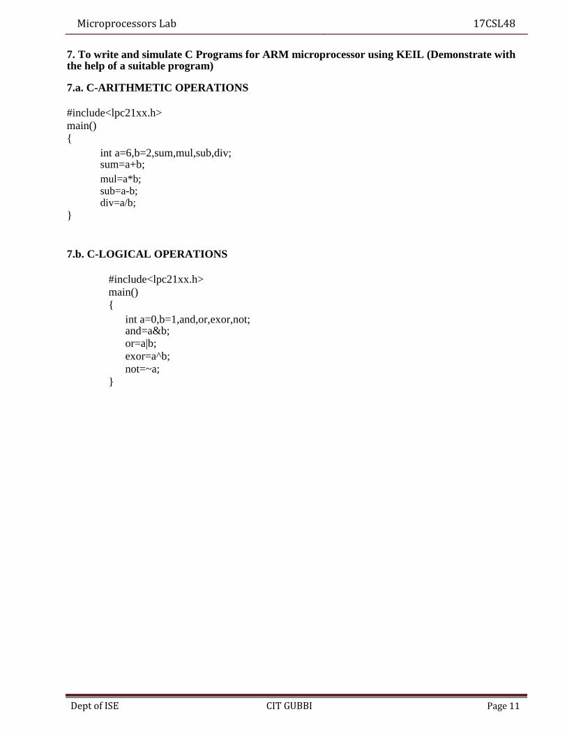
7. To write and simulate C Programs for ARM microprocessor using KEIL (Demonstrate with the help of a suitable program) 7.a. C-ARITHMETIC OPERATIONS #include<lpc21xx.h>
main()
{ int a=6,b=2,sum,mul,sub,div; sum=a+b; mul=a*b; sub=a-b; div=a/b;
}
7.b. C-LOGICAL OPERATIONS
#include<lpc21xx.h>
main()
{ int a=0,b=1,and,or,exor,not; and=a&b; or=a|b;
exor=a^b;
not=~a;
}
Dept of ISE CIT GUBBI Page 11
Microprocessors Lab 17CSL48
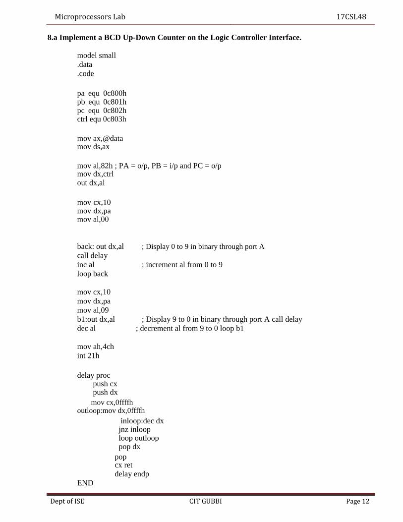
8.a Implement a BCD Up-Down Counter on the Logic Controller Interface.
model small
.data
.code
pa equ 0c800h pb equ 0c801h pc equ 0c802h ctrl equ 0c803h
mov ax,@data mov ds,ax
mov al,82h ; PA = o/p, PB = i/p and PC = o/p mov dx,ctrl out dx,al
mov cx,10 mov dx,pa mov al,00
back: out dx,al ; Display 0 to 9 in binary through port A
call delay
inc al ; increment al from 0 to 9
loop back
mov cx,10
mov dx,pa
mov al,09
b1:out dx,al ; Display 9 to 0 in binary through port A call delay
dec al ; decrement al from 9 to 0 loop b1
mov ah,4ch
int 21h
delay proc
push cx push dx
mov cx,0ffffh outloop:mov dx,0ffffh
inloop:dec dx jnz inloop loop outloop pop dx
pop cx ret delay endp
END
Dept of ISE CIT GUBBI Page 12
Microprocessors Lab 17CSL48
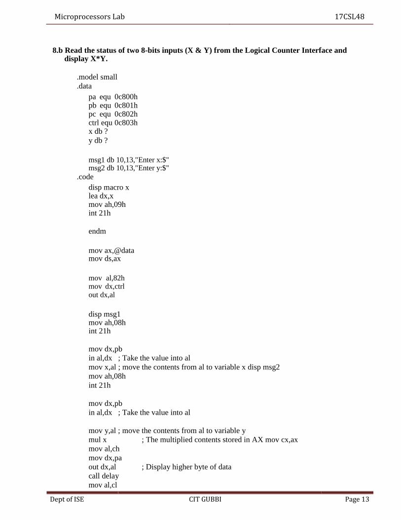
8.b Read the status of two 8-bits inputs (X & Y) from the Logical Counter Interface and display X*Y.
.model small
.data pa equ 0c800h pb equ 0c801h pc equ 0c802h ctrl equ 0c803h x db ? y db ?
msg1 db 10,13,"Enter x:$" msg2 db 10,13,"Enter y:$"
.code disp macro x lea dx,x mov ah,09h int 21h
endm
mov ax,@data mov ds,ax
mov al,82h mov dx,ctrl out dx,al
disp msg1 mov ah,08h int 21h
mov dx,pb
in al,dx ; Take the value into al
mov x,al ; move the contents from al to variable x disp msg2
mov ah,08h
int 21h
mov dx,pb
in al,dx ; Take the value into al
mov y,al ; move the contents from al to variable y
mul x ; The multiplied contents stored in AX mov cx,ax
mov al,ch
mov dx,pa
out dx,al ; Display higher byte of data
call delay
mov al,cl
Dept of ISE CIT GUBBI Page 13
Microprocessors Lab 17CSL48
mov dx,pa
out dx,al ; Display lower byte of data
mov ah,4ch
int 21h
8.b Read the status of two 8-bits inputs (X & Y) from the Logical Counter Interface and display X*Y.
.model small .data .code
pa equ 0c800h pb equ 0c801h pc equ 0c802h ctrl equ 0c803h x db ? y db ? msg1 db 10,13,"Enter x:$" msg2 db 10,13,"Enter y:$"
disp macro x
lea dx,x mov ah,09h int 21h endm
mov ax,@data mov ds,ax
mov al,82h mov dx,ctrl out dx,al
disp msg1 mov ah,08h int 21h
mov dx,pb
in al,dx ;Take the value into al
mov x,al ; move the contents from al to variable x disp
msg2 mov ah,08h
int 21h
mov dx,pb in al,dx ; Take the value into al
mov y,al ; move the contents from al to variable y
mul x ; The multiplied contents stored in AX mov cx,ax
mov al,ch
Dept of ISE CIT GUBBI Page 14
Microprocessors Lab 17CSL48
mov dx,pa
out dx,al ; Display higher byte of data
call delay
mov al,cl
mov dx,pa out dx,al ; Display lower byte of data
mov ah,4ch
int 21h
delay proc push cx
push dx
mov cx,0ffffh
outloop:mov dx,0ffffh inloop:dec dx
jnz inloop
loop outloop
pop dx
pop cx
ret delay endp
end
Dept of ISE CIT GUBBI Page 15
Microprocessors Lab 17CSL48
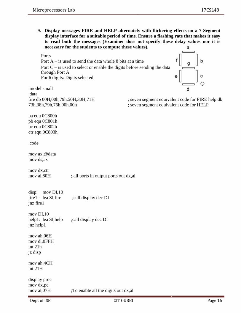
9. Display messages FIRE and HELP alternately with flickering effects on a 7-Segment
display interface for a suitable period of time. Ensure a flashing rate that makes it easy
to read both the messages (Examiner does not specify these delay values nor it is
necessary for the students to compute these values).
Ports
Port A – is used to send the data whole 8 bits at a time Port C – is used to select or enable the digits before sending the data through Port A For 6 digits: Digits selected
.model small
.data
fire db 00H,00h,79h,50H,30H,71H ; seven segment equivalent code for FIRE help db
73h,38h,79h,76h,00h,00h ; seven segment equivalent code for HELP
pa equ 0C800h
pb equ 0C801h
pc equ 0C802h
ctr equ 0C803h
.code
mov ax,@data
mov ds,ax
mov dx,ctr
mov al,80H ; all ports in output ports out dx,al
disp: mov DI,10
fire1: lea SI,fire ;call display dec DI
jnz fire1
mov DI,10
help1: lea SI,help ;call display dec DI
jnz help1
mov ah,06H
mov dl,0FFH
int 21h
jz disp
mov ah,4CH
int 21H
display proc
mov dx,pc
mov al,07H ;To enable all the digits out dx,al
Dept of ISE CIT GUBBI Page 16
Microprocessors Lab 17CSL48
mov cx,06H
mov bl,00
back: mov al,bl ;To select one digit from digit 1 to 6 (0-5) mov dx,pc
out dx,al
mov dx,pa
Lodsb ;Send the data to the selected digit out dx,al
call delay
inc bl ; increment bl to select next higher digit loop back
ret display endp
delay proc push CX push dx mov cx,0FFFH
outloop: mov dx,0FFFH inloop: dec dx jnz inloop loop outloop
pop dx pop cx ret delay endp end
Dept of ISE CIT GUBBI Page 17
Microprocessors Lab 17CSL48
10. Drive a Stepper Motor interface to rotate the motor in specified direction (clockwise or counter-clockwise) by N steps (Direction and N are specified by the examiner). Introduce suitable delay between successive steps. (Any arbitrary value for the delay may be assumed by the student).
.model small
.data
.code
pa equ 0c800h pb equ 0c801h pc equ 0c802h cr equ 0c803h count db 10
mov ax,@data mov ds,ax mov dx,cr mov al,80h out dx,al mov bh,count
mov al,88h ; at a time one coil is selected
up:mov dx,pc out dx,al call delay ror al,1 ; rotate anticlockwise dec bh jnz up mov bh,count mov dx,pc mov al,88h back: out dx,al call delay rol al,1 ; rotate clockwise dec bh jnz back mov ah,4ch int 21h
delay proc push cx push dx mov cx,8000h outloop:mov dx,4000h inloop: dec dx jnz inloop loop outloop pop dx pop cx ret
Dept of ISE CIT GUBBI Page 18
Microprocessors Lab 17CSL48
delay endp
end
Dept of ISE CIT GUBBI Page 19

Microprocessors Lab 17CSL48
11.a Generate the Sine Wave using DAC interface (The output of the DAC is to be displayed on the CRO).
Calculate table values using the formula table[i]=127+127 Sin ( Equation to generate sine wave) Where ranges from 0 to 180 in steps of 6 degree
.MODEL SMALL
.DATA
pa equ 0c800h pb equ 0c801h pc equ 0c802h ctrl equ 0c803h
TABLE DB
127,140,153,166,178,190,201,211,221,229,236,243,247,251,253,254,253,251,24 7,243,236,229,221,211,201,190,178,166,153,140,127
Dept of ISE CIT GUBBI Page 20

Microprocessors Lab 17CSL48
.CODE
MOV AX,@DATA ; initialize the data segment MOV DS,AX
MOV AL,80H ; 80h is the control word MOV DX,ctrl ; ctrl reg addr
OUT DX,AL ; ctrl word is moved to ctrl reg
BEGIN : MOV DX,pa ; Port A address
LEA SI,TABLE ; SI points to beginning of table MOV CX,31
; CX is moved with 31
BACK : MOV AL,[SI] ; [SI] is moved to AL OUT DX,AL
INC SI ; increment SI
LOOP BACK ; loop to print all values in table MOV AL,127
; move 127(reference line) to AL
MOV CX,31 ; move 31 to CX
BACK1 : OUT DX,AL ; display AL
LOOP BACK1 ; loop back1 print all value
MOV AH,06H
MOV DL,0FFH
INT 21H
JZ BEGIN ; if no key is pressed goes to begin
MOV AH,4CH ; terminate the program
INT 21H
END ; end of program
11.b Generate a Half Rectified Sine wave form using the DAC interface. (The output of the DAC is to be displayed on the CRO).
.MODEL SMALL
.DATA
pa equ 0c800h pb equ 0c801h pc equ 0c802h ctrl equ 0c803h
TABLE DB 127,140,153,166,170,190,201,211,221,229,236,243,247,251,253
DB 254,253,251,247,243,236,229,221,211,201,190,178,166,153,140,127
.CODE
MOV AX,@DATA ; initialize data segment
MOV DS,AX
Dept of ISE CIT GUBBI Page 21
Microprocessors Lab 17CSL48
MOV AL,80H ; 80h is control word
MOV DX,ctrl ; ctrl reg addr
OUT DX,AL ; ctrl word is moved to ctrl reg
BEGIN : MOV DX,pa ; Port A address
LEA SI,TABLE ; SI points to 1st position of table
MOV CX,31 ; 31 (total no of values) is mov to CX
BACK : MOV AL,[SI]
OUT DX,AL
INC SI ; increment SI
LOOP BACK ; loop decrements the CX register value
MOV AH,06H
MOV DL,0FFH
INT 21H
JZ BEGIN ; if no key is pressed goes to begin
MOV AH,4CH ; terminate the program INT 21H
END ; end of program
Dept of ISE CIT GUBBI Page 22
Microprocessors Lab 17CSL48
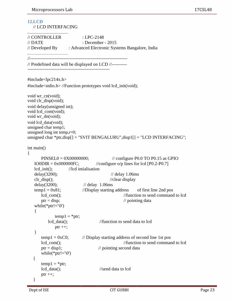
12.LCD
// LCD INTERFACING
//----------------------------------------------------------------
// CONTROLLER : LPC-2148
// DATE : December - 2015
// Developed By : Advanced Electronic Systems Bangalore, India
//----------------------------------------------------------------
//---------------------------------------------------------------- // Predefined data will be displayed on LCD //----------------------------------------------------------------
#include<lpc214x.h> #include<stdio.h> //Function prototypes void lcd_init(void);
void wr_cn(void); void clr_disp(void); void delay(unsigned int); void lcd_com(void); void wr_dn(void); void lcd_data(void); unsigned char temp1; unsigned long int temp,r=0; unsigned char *ptr,disp[] = "SVIT BENGALURU",disp1[] = "LCD INTERFACING";
int main()
{
PINSEL0 = 0X00000000; // configure P0.0 TO P0.15 as GPIO
IO0DIR = 0x000000FC; //configure o/p lines for lcd [P0.2-P0.7]
lcd_init(); //lcd intialisation
delay(3200); // delay 1.06ms
clr_disp(); //clear display
delay(3200); // delay 1.06ms
temp1 = 0x81; //Display starting address of first line 2nd pos
lcd_com(); //function to send command to lcd
ptr = disp; // pointing data
while(*ptr!='\0')
{
temp1 = *ptr;
lcd_data(); //function to send data to lcd
ptr ++;
}
temp1 = 0xC0; // Display starting address of second line 1st pos
lcd_com(); //function to send command to lcd
ptr = disp1; // pointing second data while(*ptr!='\0')
{
temp1 = *ptr;
lcd_data(); //send data to lcd
ptr ++;
}
Dept of ISE CIT GUBBI Page 23

Microprocessors Lab 17CSL48
while(1);
} //end of main()
// lcd initialisation routine.
void lcd_init(void)
{
temp = 0x30; //command to test LCD voltage level
wr_cn();
delay(3200);
temp = 0x30; //command to test LCD voltage level
wr_cn();
delay(3200);
temp = 0x30; //command to test LCD voltage level
wr_cn();
delay(3200);
temp = 0x20; // change to 4 bit mode from default 8 bit mode
wr_cn();
delay(3200);
temp1 = 0x28; // load command for lcd function setting with lcd in 4 bit mode,
lcd_com(); // 2 line and 5x7 matrix display
delay(3200);
temp1 = 0x0C; // load a command for display on, cursor on and blinking off
lcd_com();
delay(800);
temp1 = 0x06; // command for cursor increment after data dump
lcd_com();
delay(800);
temp1 = 0x80; // set the cursor to beginning of line 1
lcd_com();
delay(800);
}
void lcd_com(void)
{
temp = temp1 & 0xf0; //masking higher nibble first
wr_cn();
temp = temp1 & 0x0f; //masking lower nibble
temp = temp << 4;
wr_cn();
delay(500); // some delay
}
// command nibble o/p routine
void wr_cn(void) //write command reg
{
IO0CLR = 0x000000FC; // clear the port lines.
IO0SET= temp; // Assign the value to the PORT lines
IO0CLR = 0x00000004; // clear bit RS = 0
IO0SET= 0x00000008; // E=1
Dept of ISE CIT GUBBI Page 24
Microprocessors Lab 17CSL48
delay(10);
IO0CLR = 0x00000008; //E=0
}
// data nibble o/p routine
void wr_dn(void) ////write data reg
{
IO0CLR = 0x000000FC; // clear the port lines.
IO0SET = temp; // Assign the value to the PORT lines
IO0SET = 0x00000004; // set bit RS = 1
IO0SET = 0x00000008; // E=1
delay(10);
IO0CLR = 0x00000008; //E=0
} // data o/p routine which also outputs high nibble first
// and lower nibble next
void lcd_data(void)
{
temp = temp1 & 0xf0; //masking higher nibble first
temp = temp ;
wr_dn();
temp= temp1 & 0x0f; //masking lower nibble
temp= temp << 4; //shift 4bit to left
wr_dn();
delay(100);
}
void clr_disp(void) // function to clear the LCD screen
{
temp1 = 0x01;
lcd_com();
delay(500);
}
void delay(unsigned int r1) // delay function using for loop
{
for(r=0;r<r1;r++);
}
Dept of ISE CIT GUBBI Page 25
Microprocessors Lab 17CSL48
13.STEPPER
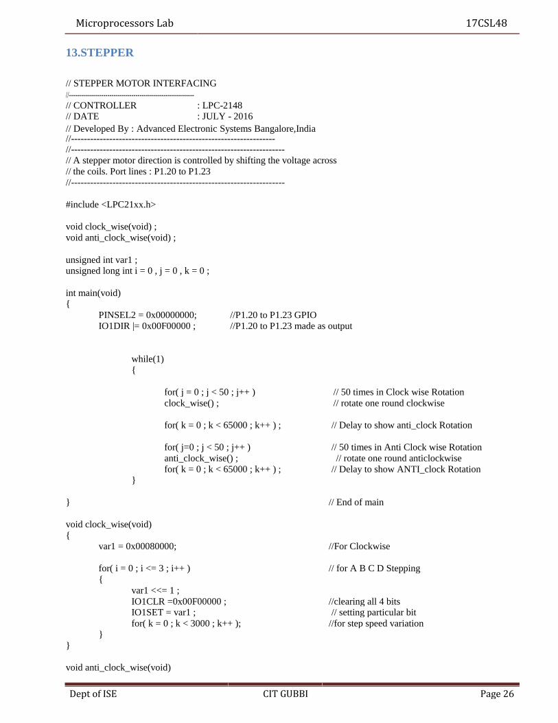
// STEPPER MOTOR INTERFACING //-------------------------------------------------------------- // CONTROLLER : LPC-2148 // DATE : JULY - 2016 // Developed By : Advanced Electronic Systems Bangalore,India //---------------------------------------------------------------- //-------------------------------------------------------------------
// A stepper motor direction is controlled by shifting the voltage across // the coils. Port lines : P1.20 to P1.23 //------------------------------------------------------------------- #include <LPC21xx.h>
void clock_wise(void) ; void anti_clock_wise(void) ;
unsigned int var1 ; unsigned long int i = 0 , j = 0 , k = 0 ;
int main(void) {
PINSEL2 = 0x00000000; //P1.20 to P1.23 GPIO
IO1DIR |= 0x00F00000 ; //P1.20 to P1.23 made as output
while(1) {
for( j = 0 ; j < 50 ; j++ ) // 50 times in Clock wise Rotation clock_wise() ; // rotate one round clockwise
for( k = 0 ; k < 65000 ; k++ ) ; // Delay to show anti_clock Rotation
for( j=0 ; j < 50 ; j++ ) // 50 times in Anti Clock wise Rotation anti_clock_wise() ; // rotate one round anticlockwise for( k = 0 ; k < 65000 ; k++ ) ; // Delay to show ANTI_clock Rotation
}
} // End of main
void clock_wise(void) {
var1 = 0x00080000; //For Clockwise
for( i = 0 ; i <= 3 ; i++ ) // for A B C D Stepping {
var1 <<= 1 ;
IO1CLR =0x00F00000 ; //clearing all 4 bits IO1SET = var1 ; // setting particular bit for( k = 0 ; k < 3000 ; k++ ); //for step speed variation
}
}
void anti_clock_wise(void)
Dept of ISE CIT GUBBI Page 26

Microprocessors Lab 17CSL48
{ var1 = 0x00800000 ; //For Anticlockwise IO1CLR =0x00F00000 ; //clearing all 4 bits IO1SET = var1 ;
for( k = 0 ; k < 3000 ; k++ ) ;
for( i = 0 ; i < 3 ; i++ ) // for A B C D Stepping {
var1 >>=1; //rotating bits IO1CLR =0x00F00000 ; // clear all bits before setting
IO1SET = var1 ; // setting particular bit
for( k = 0 ; k < 3000 ; k++ ) ; //for step speed variation
} }
VIVA QUESTION AND ANSWERS
1. Define Microprocessor
The Processor is an integrated circuit in a small size and hence the name microprocessor.
2. How many bit is 8086 Microprocessor
8086 is a 16-bit microprocessor.
3. How many bits are 8086 data and address bus
Data bus – 16 bit and address bus – 20 bit.
4. How many 16-bit register are available in 8086. Name them
Dept of ISE CIT GUBBI Page 27

Microprocessors Lab 17CSL48
There are 14, 16-bit register. They are AX, BX, CX, DX- general purpose registers, CS, SS,
ES, DS- Segment registers, SI, DI, SP, BP, IP – Index and pointer registers and Flag register,
5. Name 2 modes in which 8086 can work?
8086 can work in
i) Minimum mode- when only one 8086 CPU is used.
ii) Maximum mode – when more than one processor (multiprocessor) is used.
6. What is the function of AX register?
AX is used as 16-bit Accumulator.
7. What does segment register hold?
Segment registers are used to hold the upper 16-bits of the starting addresses of the 4 memory
segments.
8. What is the size of the memory in 8086?
Maximum Size of memory in 8086 is 1Mega byte.
9. What is the maximum size of each segment in 8086 Microprocessor
Maximum Size of each segment in 8086 is 64K byte.
10. What does pointer registers hold?
The pointer register IP, BP and SP holds the offset within the code, data, and stack segments.
11. What does index register hold?
SI –Source Index register hold the offset of a data word in the data segment. 20-bit physical data
address is calculated from SI and DS.
DI- Destination Index register hold the offset of a data word in the extra segment. 20-bit physical
data address is calculated from DI and ES.
12. How many active flags are there in 8086? Name them.
There are 9 active flags. They are Carry Flag, Parity Flag, Auxillary Flag, Zero Flag, Sign Flag, and
Overflow Flag.
13. Explain the working of PUSH operation
PUSH operation decrements the stack pointer by 2 and copies a word from some source to
the location in the stack where the stack pointer points.
14. Explain the working of POP operation
POP operation copies a word from the stack location pointed by the stack pointer to the destination
and then stack pointer is automatically incremented by 2,
Dept of ISE CIT GUBBI Page 28

Microprocessors Lab 17CSL48
15. Explain the different types of instructions in 8086
Data transfer instruction, Arithmetic and Logical instruction, Shift and Rotate instructions, String
instructions, Jump instructions, Machine Control and Miscellaneous instructions and Interrupt
instructions.
16. What is the use of DUP directive?
Dup directive can be used to initialize several locations and to assign value to these locations.
17. List the directives used to define different types of variables
DB- Define Byte
DW- Define Word
DD- Define Doubleword DQ- Define Quadword DT- Define Terabytes.
18. List some Data Transfer instructions
MOV instruction to transfer byte, PUSH/POP instructions, Load Effective address
instructions(LEA), String Data transfer instructions(MOVSB), XCHG,LAHF, SAHF, XLAT, IN
and OUT
19. List some Arithmetic and logical instructions
ADD, SUB, MUL, DIV, AND OR, NOT, TEST, CMP, AAM, AAD etc…
20. Explain how AAM instruction is executed
Syntax: AAM ; No operands
Is used to convert the binary result to 2 digit unpacked BCD
Working of AAM instruction depends on the contents of AL register.
The data entered from a keyboard will be in the ASCII format(e.g. if entered „9‟ then inside
the computer it will be stored as 39H)
Suppose AL contains 3FH i.e 63 in BCD.It can be represented in unpacked BCD as 06 03 BCD.
Example: MOV AL,15 0Fh
AAM AL=05H
21. Differentiate between TEST and AND instruction
TEST instruction performs AND operation. Difference is that the AND instruction changes the
destination operand while TEST instruction does not. TEST instruction only affects the condition of
the flag register, which indicates the result of the test.
22. SHR AL, 1. Give the equivalent meaning of this instruction
SHR-shifts each bit in the specified destination to the right. It is equivalent to divide by 2.
Dept of ISE CIT GUBBI Page 29

Microprocessors Lab 17CSL48
23. What are 2 types of JUMP instruction
Two types are Conditional and Unconditional JUMP instructions.
24. Distinguish between the instructions JA Label and JG Label
JA(Jump if Above) is used when we are comparing unsigned numbers.
JG(Jump if Greater) is used when we are comparing the signed numbers.
25. Differentiate between NEAR and FAR JUMP.
NEAR JUMP- Is 3 byte instruction, which allows a branch or jump within + 32kbytes from the
instruction in the current code segment. Only IP is changes, the content of CS remains same.
FAR JUMP- Is 5 byte instruction, which allows a jump to any memory location within the real
memory system. A FAR jump is a jump where the destination location is from a different segment.
In this case both IP and CS are changed as specified in the destination.
26. What is the other name for NEAR jump and FAR jump.
NEAR jump is also called as intersegment jump and FAR jump is also called as intrasegment jump.
27. Which instruction is used to SET and RESET direction flag ?
STD- is used set the direction flag. SI and DI are automatically decremented. CLD-
is used to reset the direction flag. SI and DI are automatically incremented.
28. Differentiate between Macro and Procedure
Sl. Procedure Macro
No.
1. Accessed by CALL and RET instruction Accessed during assembly with the name
given to macro when defined
2. Machine code for instructions is put Machine code is generated for instructions
only once in the memory each time when macro is called
3. Less memory is required More memory is required
4. Parameters can be passed in registers, Parameters passed as part of statement which
memory locations or stack calls nacro.
29. What is the default size of Stack?
Dept of ISE CIT GUBBI Page 30

Microprocessors Lab 17CSL48
Default size of stack is 64KB
30. Explain the working of XLAT instruction
XLAT instruction: Translate the value in
AL Syntax: XLAT ; No operands
Instruction replaces a byte in AL register with a byte from a lookup table in memory.
BX register stores the offset of the starting address of the lookup table and AL register stores the
byte number from the lookup table.
The instruction copies byte from address pointed by [BX+AL] back into AL
Equivalent MOVE instruction is MOV AL,[AL][BX]
Use of XLAT instruction in Program 6b.
i) Store in the data segment; say for example starting from offset location 4000H, the table
of 7-segment equivalent code in hexadecimal. For example, the character „6‟ has the
ASCII code of 36H and 7 segment equivalent code of 7DH (refer 7 segment equivalent
code table). Thus 7DH is stored in location 4036H.
ii) To convert the ASCII code of 36H to 7 segment equivalent code of 7Dh, we must
execute XLAT instruction with AL contents 36H and BX contents as 4000H. This
results in AL contents changing to 7DH.
Before After
(AL) 36 7DH
(BX) 4000 4000
(DS:36[BX] 7D 7D
31. What are assembler directives. Name few of them.
.model, dw,dd,db etc
32. List the memory model available in 8086.
Small, medium, compact
33. Differentiate between arithmetic and logical shift instructions
Logical shifts move a 0 into the rightmost bit position for a logical left shift(SHL) and 0 to the leftmost bit
position for a logical right shift(SHR). Arithmetic left shift(SAL) and SHL are identical
but arithmetic right shift (SAR) copies the sign bit through the number, while logical right shift
copies a 0 through the number.
34. Define interrupt
Dept of ISE CIT GUBBI Page 31
Microprocessors Lab 17CSL48
When a microprocessor is interrupted it stops executing its current program and calls a special
routine which services the interrupt. The event that causes the interruption is called interrupt.
Special routine executed to the service is called Interrupt Service Routine (ISR).
35. Which are the 3 ways by which a normal program can be interrupted
3 ways are:
1. By External Signal – applied to NMI or INTR input pin
2. Special Instruction in the program – Eg INT
3. By the occurrence of some condition – Divide by zero, overflow etc.
36. Differentiate between hardware and software interrupts
Interrupt caused by an external signal is referred to as hardware interrupt. Conditional interrupts or
interrupts caused by special instructions are called software interrupts.
37. What is interrupt vector table
In 8086 system the first 1Kbyte of memory is reserved for storing the starting addresses of interrupt
service routines. This block of memory is called as Interrupt Vector table or interrupt pointer table.
38. How many interrupts service routines can be stored in the interrupt vector table
Table can hold the starting addresses for 256 interrupt service routines.
39. Name the dedicated interrupt types.
a) Divide By Zero Interrupt(Type 0)
b) Single Step Interrupt(Type 1)
c) Non-Maskable Interrupt(Type 2)
d) Breakpoint Interrupt(Type 3)
e) Overflow Interrupt( Type 4)
40. What is 8255?
8255 is a general purpose programmable I/O device used for parallel data transfer.
1. What are the operation modes of 8255?
Two basic modes are Bit Set/Reset(BSR) mode and I/O mode.
2. How 20 bit address generated using 16 bit register?
8086 generates 20-bit address using the contents of segment register and offset register associate d
with it. For Eg: the contents of CS register are multiplied by 16 (10 H) i.e shifted by 4 position to the
left by inserting zero bits and then the offset i.e the contents of IP register are added to the shifted
contents of CS to generate 20 bit physical address.
CS register- 348A H after appending zero to the left it becomes 348A0 H. IP
Dept of ISE CIT GUBBI Page 32

Microprocessors Lab 17CSL48
register – 4214.
20 bit physical address – 348A0+4214=38AB4.
3. Difference between DIV and IDIV
DIV instruction is used to divide unsigned word by a byte or to divide an unsigned double word by
a word.
IDIV instruction is used to divide signed word by a signed byte or to divide a signed double word by
a signed word.
4. Difference between MUL and IMUL
MUL instruction is used multiplies an unsigned byte from source and unsigned byte in AL.
IMUL instruction multiplies a signed byte from some source and a signed byte in AL.
5. Why is NOP instruction required?
NOP instruction does nothing but takes 3 clock cycles of processor time to execute.
6. What is the default registers used in string instructions?
Source index register (SI) and Destination index register (DI) are the default registers used in string
instructions.
7. What is the difference between JE and JZ?
JE (Jump if Zero) and JZ (Jump if Zero Flag) is same but the difference is JE is used after CMP
instruction whereas JZ is used after the arithmetic operation.
41. Differentiate between SUB and CMP
SUB instruction - subtracts the number in the source from the number in the destination and put the
result in the destination.
CMP instruction – Compares a byte/word from the specified source with a byte/word from the
specified destination. The comparison is done by subtracting the source byte or word from the
destination byte/word. But the result is not stored in the destination. Source and destination remain
unchanged, only flags are updated.
42. Generate single instruction
MOV DX, AX
MOV AX, BX
MOV BX, DX just like any other
Single instruction is XCHG AX, BX
Dept of ISE CIT GUBBI Page 33
Microprocessors Lab 17CSL48
43. Which register is affected when LOOP instruction is used?
CX register is affected when LOOP instruction is used.
44. What is the DOS function call invoked to create a file?
3CH is the Service number to create a file.
45. What is the DOS function call invoked to delete a file?
41H is the service number to delete a file.
46. Which are the 2 interrupt pin available in 8086?
INTR – Interrupt pin
NMI- Non maskable Interrupt input pin.
47. What is the DOS function to read a character from the keyboard
01H is the service number to read a character from the keyboard and read character will be stored in
AL register.
48. What is the DOS function to display string on the output screen
09H is the service number to display string on the output screen and the effective address of the
string to be displayed should be stored in DX register
Dept of ISE CIT GUBBI Page 34