bcm53128 data sheet - au.mouser.com
TRANSCRIPT

53128-DS07-R
Corporate Headquarters: San Jose, CA April 6, 2016
Data Sheet
BCM53128
Multiport Gigabit Ethernet SwitchesGENERAL DESCRIPTION
The Broadcom® BCM53128 is a highly integrated,cost-effective unmanaged-smart gigabit switch. Theswitch design is based on the field-proven, industry-leading ROBO architecture. This device combinesall the functions of a high-speed switch systemincluding packet buffers, PHY transceivers, mediaaccess controllers (MACs), address management,port-based rate control, and a non-blocking switchfabric into a single 65-nm CMOS device. Designedto be fully compliant with the IEEE 802.3™ andIEEE 802.3x specifications, including the MAC-control PAUSE frame, the BCM53128 providescompatibility with all industry-standard Ethernet,Fast Ethernet, and Gigabit Ethernet (GbE) devices.
The BCM53128 has a rich feature set suitable fornot only standard GbE connectivity for desktop andlaptop PCs, but also for next-generation gamingconsoles, set-top boxes, networked DVD players,and home theater receivers. It is also specificallydesigned for next generation SOHO/SMB routersand gateways.
The BCM53128 contains eight full-duplex 10/100/1000BASE-TX Ethernet transceivers.
The BCM53128 provides 70+ on-chip MIB countersto collect receive and transmit statistics for eachport.
The BCM53128 is available in commercialtemperature (C-Temp) and industrial temperature (I-Temp) rated packages. The BCM53128 is providedin a 256-pin eLQFP (28 mm x 28 mm) package.
FEATURES
• Nine 10/100/1000 media access controllers• Eight port 10/100/1000BASE-T/Tx transceivers• One GMII/RGMII/MII/RvMII/TMII/RvTMII
interface for an in-band management port (IMP)for connection to a CPU/management entitywithout PHY
• IEEE 802.1p, MAC, Port, TOS, and DiffServ QoSfor four queues, plus two time sensitive queues
• Port-based VLAN• IEEE 802.1Q-based VLAN with 4K entries• MAC-based trunking with automatic link failover• Port-based rate control• Port mirroring• BroadSync® HD for IEEE 802.1AS support
– Timestamp tagging at MAC interface– Time-aware egress scheduler
• DOS attack prevention– Support IPv6
• IGMP snooping, MLD snooping support• Green mode support• Spanning tree support (multiple spanning trees–
up to eight)• Loop detection for unmanaged configurations
with Broadcom’s patented LoopDTech™technology
• CableChecker™ with unmanaged mode support• Double tagging/QinQ• IEEE 802.az EEE (Energy Efficient Ethernet)
support• IEEE 802.3as support• IEEE 802.3x programmable per-port flow control
and backpressure, with IEEE 802.1x support forsecure user authentication
• EEPROM, MDC/MDIO, and SPI Interfaces• Serial Flash Interface for accessing embedded
8051 processor• 4K entry MAC address table with automatic
learning and aging• 192 KB packet buffer• 256 multicast group support• Jumbo frame support up to 9720 bytes• Serial and parallel LED interface• 1.2V for core and 3.3V for I/O• JTAG support• 256 eLQFP
Broadc
om C
onfid
entia
l

© 2016 by Broadcom. All rights reserved.
Broadcom®, the pulse logo, Connecting everything®, the Connecting everything logo, and AvagoTechnologies are among the trademarks of Broadcom and/or its affiliates in the United States, certain othercountries and/or the EU. Any other trademarks or trade names mentioned are the property of their respective
owners.
Broadcom reserves the right to make changes without further notice to any products or data herein to improvereliability, function, or design.
Information furnished by Broadcom is believed to be accurate and reliable. However, Broadcom does notassume any liability arising out of the application or use of this information, nor the application or use of anyproduct or circuit described herein, neither does it convey any license under its patent rights nor the rights of
others.
This data sheet (including, without limitation, the Broadcom component(s) identified herein) is not designed,intended, or certified for use in any military, nuclear, medical, mass transportation, aviation, navigations,
pollution control, hazardous substances management, or other high-risk application. BROADCOMPROVIDES THIS DATA SHEET “AS-IS,” WITHOUT WARRANTY OF ANY KIND. BROADCOM DISCLAIMS
ALL WARRANTIES, EXPRESSED AND IMPLIED, INCLUDING, WITHOUT LIMITATION, THE IMPLIEDWARRANTIES OF MERCHANTABILITY, FITNESS FOR A PARTICULAR PURPOSE, AND NON-
INFRINGEMENT.
Figure 1: Functional Block Diagram
Broadc
om C
onfid
entia
l

Revision HistoryBCM53128 Data Sheet
Broadcom®
April 6, 2016 • 53128-DS07-R Page 3BROADCOM CONFIDENTIAL
Revision History
Change Description Customer Impact Action Items
Revision: 53128-DS07-R
Date: 04/06/16
Updated:
• “Transmit Output Port Queues” onpage 90
Corrected typo for entriesnumber.
No action required.
• Table 291: “EEE GLB Congst THRegister (Page 92h: Address C4h),” onpage 293
Corrected typo for entriesnumber.
No action required.
• Table 293: “EEE TXQ Cong TH Register(Page 92h: Address C6h),” on page 293
Corrected typo for entriesnumber.
No action required.
Added:
• Table 324: “BCM53128IQLE Packagewith Heat Sink, 4-layer Board, P=3.1W,”on page 315
– No action required.
Revision: 53128-DS06-R
Date: 06/02/14
Updated:
• Table 324: “Ordering Information,” onpage 318
Added ordering information forpart numberBCM53128IQLE(G)
No action required.
Revision: 53128-DS05-R
Date: 02/18/13
Updated:
• Default bits 13, 12, 8, and 6 in Table 128on page 197.
• Default bits 11, 10, 8, 7, 6, and 5 inTable 132 on page 200.
• Default bits 12, 11, 10, 9, and 8 inTable 137 on page 205.
• Table 321: “Ordering Information,” onpage 319.
Revision: 53128-DS04-R
Date: 07/21/11
Updated:
• General Description Updated the generaldescription.
No action required.
Broadc
om C
onfid
entia
l
Revision HistoryBCM53128 Data Sheet
Broadcom®
April 6, 2016 • 53128-DS07-R Page 4BROADCOM CONFIDENTIAL
• Section 12: “Ordering Information,” onpage 319
Added ordering information forpart numberBCM53128VIQLE(G)
No action required.
Revision: 53128-DS03-R
Date: 12/13/10
Updated:
• “IGMP Snooping” on page 49 None. No action required.• “Loop Detection” on page 52 Updated referenced document. No action required.• “Address Resolution and Frame
Forwarding” on page 59Edited the forward field. Corrected typo.
• “Multicast Addresses” on page 61 Removed reference toIP_MULTICAST bit.
No action required.
• Table 8: “Multicast Forward FieldDefinitions,” on page 61
Replaced IP_MULTICASTcolumn with UNICAST/MULTICAST column andupdated the forwarding field.
No action required.
• Table 9: “Address Table Entry forMulticast Address,” on page 61
Replaced IPMCO withFWD_PRT_MAP.
No action required.
• “Energy Efficient Ethernet Mode” onpage 66
Updated referenced document. No action required.
• “Serial Flash Interface” on page 95 Updated SRAM value. No action required.• Figure 44: “Write Access to the Register
Set Using the PseudoPHY (PHYAD =11110) MDC/MDIO Path,” on page 119
Changed Read MII Register 27to Write Register 27.
Corrected typo.
• Table 29: “Signal Type Definitions,” onpage 126
Updated XTALO signaldescription and added GPIOpins.
No action required.
• Section 6: “Pin Assignment,” on page139
Updated pin assignments toinclude GPIO pins.
New feature option available.
• “BCM53128KQLE Pin List by BallName” on page 141
Updated pin list to include GPIOpins
New feature option available.
• Table 31: “Control Registers (Page00h),” on page 145
Added addresses B0h-B7h andB8h-BFh to table.
No action required.
• “PHY Identifier Register (Page 10h–17h:Address 04h)” on page 199
Edited binary OUI. Corrected typo.
• Table 170: “Expansion Register 45h:Transmit CRC,” on page 233
Added addresses B8h-BBh andBCh-BFh
No action required.
• Table 295: “Absolute MaximumRatings,” on page 299
Updated maximum value forelectrostatic discharge (VESD)
Corrected typo.
• Table 297: “Electrical Characteristics,”on page 300
Updated XTALI minimum andmaximum.
No action required.
• Figure 64: “SPI Timings, SS AssertedDuring SCK High,” on page 313
Updated figure. No action required.
• Table 316: “SPI Timings,” on page 313 Added time interval rows No action required.Added:
Change Description Customer Impact Action Items
Broadc
om C
onfid
entia
l
Revision HistoryBCM53128 Data Sheet
Broadcom®
April 6, 2016 • 53128-DS07-R Page 5BROADCOM CONFIDENTIAL
“GPIO ” on page 95 New feature option available.Revision: 53128-DS02-R
Date: 09/08/10
Updated:
• “Deep Green Mode” on page 66. None. No action required.• Figure 45: “LED Interface Register
Structure Diagram,” on page 121.Correct editing errors. No action required.
• Table 29: “Signal Type Definitions,” onpage 125.
Power interface descriptionupdate to change core powerfrom 1.1V to 1.2V.
Suggest a review of theschematics.
• Table 82: “Aging Time Control Register(Page 02h: Address 06h–09h),” onpage 169.
Descriptions updated. Typo correction.
• “Absolute Maximum Ratings” onpage 297.
Updated core value absolutemaximum rating value.
Suggest a review of theschematics.
• “Recommended Operating Conditions”on page 297.
Updated core voltage 1.2Vminimum and maximum valueof recommended operatingconditions.
Suggest a review of theschematics.
• “Electrical Characteristics” on page 298. Updated maximum powerconsumption by core 1.2V andIO 3.3V.
Suggest a review of theschematics.
• Section 11: “Mechanical Information,” onpage 316.
Correct editing errors. No action required.
Document Number Date Change Description
53128-DS01-R 04/02/10 Updated:
• Table 3: “Bucket Bit Rate,” on page 44.• Section 6: “Pin Assignment,” on page 137.• Section 7: “Register Definitions,” on page 141.• Section 8: “Electrical Characteristics,” on page 296.• Section 9: “Timing Characteristics,” on page 298.• Section 10: “Thermal Characteristics,” on page 313.
Added:
• “TMII (Turbo MII) and RvTMII (Reverse TMII) Interface” onpage 91.
• “Signal Descriptions” on page 124.• “LED Control Register (Page 00h: Address 1Ch)” on page 152.• “IMP RGMII Control Register (Page 00h: Address 60h)” on
page 160.• “Page 03h: Interrupt Control Register” on page 175.• “Page 92h: EEE Control Register” on page 287.
53128-DS00-R 12/17/09 Initial release.
Change Description Customer Impact Action Items
Broadc
om C
onfid
entia
l
Table of ContentsBCM53128 Data Sheet
Broadcom®
April 6, 2016 • 53128-DS07-R Page 6
BROADCOM CONFIDENTIAL
Table of Contents
About This Document ................................................................................................................................ 30
Purpose and Audience.......................................................................................................................... 30
Acronyms and Abbreviations................................................................................................................. 30
Document Conventions ......................................................................................................................... 30
References ............................................................................................................................................ 31
Technical Support ...................................................................................................................................... 31
Section 1: Introduction ..................................................................................................... 32
Overview...................................................................................................................................................... 32
Section 2: Features and Operation .................................................................................. 33
Overview of Features and Operation........................................................................................................ 33
Quality of Service ....................................................................................................................................... 34
Egress Transmit Queues....................................................................................................................... 35
Port-Based QoS .................................................................................................................................... 35
IEEE 802.1p QoS.................................................................................................................................. 35
MACDA-Based QoS.............................................................................................................................. 36
TOS/DSCP QoS.................................................................................................................................... 36
TC Decision Tree .................................................................................................................................. 36
Non-BroadSync HD Frame ............................................................................................................ 36
BroadSync HD Frame.................................................................................................................... 37
Queuing Class (COS) Determination .................................................................................................... 37
Port-Based VLAN........................................................................................................................................ 38
IEEE 802.1Q VLAN...................................................................................................................................... 39
IEEE 802.1Q VLAN Table Organization................................................................................................ 39
Programming the VLAN Table................................................................................................................... 40
Double-Tagging .......................................................................................................................................... 41
ISP Port ................................................................................................................................................. 42
Customer Port ....................................................................................................................................... 42
Uplink Traffic (from Customer Port to ISP)............................................................................................ 43
Downlink Traffic (from ISP to Customer Port) ....................................................................................... 43
Jumbo Frame Support ............................................................................................................................... 44
Port Trunking/Aggregation........................................................................................................................ 44
WAN Port..................................................................................................................................................... 45
Rate Control ................................................................................................................................................ 45
Ingress Rate Control ............................................................................................................................. 45
Two-Bucket System .............................................................................................................................. 46
Egress Rate Control .............................................................................................................................. 46
Broadc
om C
onfid
entia
l
Table of ContentsBCM53128 Data Sheet
Broadcom®
April 6, 2016 • 53128-DS07-R Page 7
BROADCOM CONFIDENTIAL
Bucket Bit Rate...................................................................................................................................... 47
IMP Port Egress Rate Control ............................................................................................................... 47
Protected Ports........................................................................................................................................... 47
Port Mirroring.............................................................................................................................................. 48
Enabling Port Mirroring.......................................................................................................................... 48
Capture Port .......................................................................................................................................... 48
Mirror Filtering Rules ............................................................................................................................. 48
Port Mask Filter .............................................................................................................................. 48
Packet Address Filter ..................................................................................................................... 49
Packet Divider Filter ....................................................................................................................... 49
IGMP Snooping........................................................................................................................................... 49
MLD Snooping ............................................................................................................................................ 50
IEEE 802.1x Port-Based Security .............................................................................................................. 50
DoS Attack Prevention............................................................................................................................... 51
MSTP Multiple Spanning Tree ................................................................................................................... 52
Software Reset............................................................................................................................................ 52
Loop Detection ........................................................................................................................................... 52
BroadSync HD ............................................................................................................................................ 53
Time Base and Slot Generation ............................................................................................................ 53
Transmission Shaping and Scheduling ................................................................................................. 54
BroadSync HD Class 5 Media Traffic............................................................................................. 54
BroadSync HD Class 4 Media Traffic............................................................................................. 55
CableChecker™ .......................................................................................................................................... 56
Egress PCP Remarking.............................................................................................................................. 57
Address Management ................................................................................................................................ 57
Address Table Organization.................................................................................................................. 58
Address Learning .................................................................................................................................. 59
Address Resolution and Frame Forwarding.......................................................................................... 59
Unicast Addresses ......................................................................................................................... 59
Multicast Addresses ....................................................................................................................... 61
Reserved Multicast Addresses....................................................................................................... 62
Static Address Entries ........................................................................................................................... 63
Accessing the ARL Table Entries.......................................................................................................... 63
Reading an ARL Entry ................................................................................................................... 63
Writing an ARL Entry...................................................................................................................... 63
Searching the ARL Table ............................................................................................................... 64
Address Aging ....................................................................................................................................... 64
Fast Aging ............................................................................................................................................. 65
Using the Multiport Addresses .............................................................................................................. 65
Broadc
om C
onfid
entia
l
Table of ContentsBCM53128 Data Sheet
Broadcom®
April 6, 2016 • 53128-DS07-R Page 8
BROADCOM CONFIDENTIAL
Power Savings Modes................................................................................................................................ 65
Auto Power Down Mode........................................................................................................................ 66
Energy Efficient Ethernet Mode............................................................................................................. 66
Short Cable Mode (Green Mode) .......................................................................................................... 66
Deep Green Mode................................................................................................................................. 67
Section 3: System Functional Blocks.............................................................................. 68
Overview of System Functional Blocks ................................................................................................... 68
Media Access Controller............................................................................................................................ 68
Receive Function................................................................................................................................... 68
Transmit Function.................................................................................................................................. 69
Flow Control .......................................................................................................................................... 69
10/100 Mbps Half-Duplex............................................................................................................... 69
10/100/1000 Mbps Full-Duplex ...................................................................................................... 69
Integrated 10/100/1000 PHY....................................................................................................................... 70
Encoder ................................................................................................................................................. 70
Decoder................................................................................................................................................. 71
Link Monitor........................................................................................................................................... 71
Digital Adaptive Equalizer ..................................................................................................................... 72
Echo Canceler....................................................................................................................................... 72
Cross Talk Canceler.............................................................................................................................. 72
Analog-to-Digital Converter ................................................................................................................... 72
Clock Recovery/Generator .................................................................................................................... 73
Baseline Wander Correction ................................................................................................................. 73
Multimode TX Digital-to-Analog Converter............................................................................................ 73
Stream Cipher ....................................................................................................................................... 73
Wire Map and Pair Skew Correction ..................................................................................................... 74
Automatic MDI Crossover ..................................................................................................................... 74
10/100BASE-TX Forced Mode Auto-MDIX ........................................................................................... 75
Resetting the PHY................................................................................................................................. 75
PHY Address......................................................................................................................................... 76
Super Isolate Mode ............................................................................................................................... 76
Standby Power-Down Mode.................................................................................................................. 76
Auto Power-Down Mode ....................................................................................................................... 77
External Loopback Mode....................................................................................................................... 77
Full-Duplex Mode .................................................................................................................................. 78
Copper Mode ................................................................................................................................. 78
Master/Slave Configuration ................................................................................................................... 79
Next Page Exchange............................................................................................................................. 79
Frame Management.................................................................................................................................... 79
Broadc
om C
onfid
entia
l

Table of ContentsBCM53128 Data Sheet
Broadcom®
April 6, 2016 • 53128-DS07-R Page 9
BROADCOM CONFIDENTIAL
In-Band Management Port .................................................................................................................... 79
Broadcom Tag Format for Egress Packet Transfer............................................................................... 81
Broadcom Tag Format for Ingress Packet Transfer .............................................................................. 82
MIB Engine .................................................................................................................................................. 83
MIB Counters Per Port .......................................................................................................................... 83
Receive Only Counter (19) Description of Counter........................................................................ 83
Transmit Counters Only (19) Description of Counter ..................................................................... 85
Transmit or Receive Counters (10) Description of Counter ........................................................... 86
Integrated High-Performance Memory ..................................................................................................... 90
Switch Controller........................................................................................................................................ 90
Buffer Management............................................................................................................................... 90
Memory Arbitration ................................................................................................................................ 90
Transmit Output Port Queues ............................................................................................................... 90
Section 4: System Interfaces............................................................................................ 92
Overview of System Interfaces ................................................................................................................. 92
Copper Interface ......................................................................................................................................... 92
Auto-Negotiation.................................................................................................................................... 92
Line-side (Remote) Loopback Mode ..................................................................................................... 93
Frame Management Port Interface............................................................................................................ 93
MII Interface .......................................................................................................................................... 93
TMII (Turbo MII) and RvTMII (Reverse TMII) Interface......................................................................... 93
Reverse MII Port (RvMII)....................................................................................................................... 93
GMII Port ............................................................................................................................................... 94
RGMII Port ............................................................................................................................................ 94
Configuration Pins ..................................................................................................................................... 94
Programming Interfaces ............................................................................................................................ 95
Serial Flash Interface ............................................................................................................................ 95
GPIO ..................................................................................................................................................... 95
SPI-Compatible Programming Interface................................................................................................ 96
SS: Slave Select ............................................................................................................................ 96
SCK: Serial Clock........................................................................................................................... 96
MOSI: Master Output Slave Input .................................................................................................. 96
MISO: Master Input Slave Output .................................................................................................. 97
Without External PHY .................................................................................................................... 98
External PHY Registers ................................................................................................................. 99
Reading and Writing BCM53128 Registers Using SPI .................................................................. 99
Normal Read Operation ............................................................................................................... 100
Fast Read Operation.................................................................................................................... 104
Normal Write Operation ............................................................................................................... 107
Broadc
om C
onfid
entia
l
Table of ContentsBCM53128 Data Sheet
Broadcom®
April 6, 2016 • 53128-DS07-R Page 10
BROADCOM CONFIDENTIAL
EEPROM Interface.............................................................................................................................. 110
EEPROM Format ......................................................................................................................... 110
MDC/MDIO Interface ................................................................................................................................. 112
MDC/MDIO Interface Register Programming...................................................................................... 112
PseudoPHY......................................................................................................................................... 113
LED Interfaces .......................................................................................................................................... 119
Dual Input Configuration/LED Output Function ................................................................................... 123
Section 5: Hardware Signal Definition Table ................................................................ 124
I/O Signal Types........................................................................................................................................ 124
Signal Descriptions .................................................................................................................................. 125
Section 6: Pin Assignment ............................................................................................. 138
BCM53128KQLE Pin List by Signal Name.............................................................................................. 138
BCM53128KQLE Pin List by Ball Number .............................................................................................. 140
Section 7: Register Definitions ...................................................................................... 142
Register Definition.................................................................................................................................... 142
Register Notations.................................................................................................................................... 142
Global Page Register ............................................................................................................................... 142
Page 00h: Control Registers ................................................................................................................... 144
Port Traffic Control Register (Page 00h: Address 00h)....................................................................... 146
IMP Port Control Register (Page 00h: Address 08h) .......................................................................... 147
Switch Mode Register (Page 00h: Address 0Bh) ................................................................................ 148
IMP Port State Override Register (Page 00h: Address 0Eh) .............................................................. 148
LED Control Register (Page 00h: Address 0Fh–1Bh)......................................................................... 149
LED Refresh Register (Page 00h: Address 0Fh) ................................................................................ 149
LED Function 0 Control Register (Page 00h: Address 10h)................................................................ 150
LED Function 1 Control Register (Page 00h: Address 12h)................................................................ 151
LED Function Map Register (Page 00h: Address 14h–15h) ............................................................... 151
LED Enable Map Register (Page 00h: Address 16h–17h).................................................................. 152
LED Mode Map 0 Register (Page 00h: Address 18h–19h) ................................................................. 152
LED Mode Map 1 Register (Page 00h: Address 1Ah–1Bh) ................................................................ 152
LED Control Register (Page 00h: Address 1Ch)................................................................................. 153
PHY LED Control Register (Page 00h: Address 1Dh) ........................................................................ 153
Port Forward Control Register (Page 00h: Address 21h).................................................................... 154
Protected Port Selection Register (Page 00h: Address 24h–25h) ...................................................... 155
WAN Port Select Register (Page 00h: Address 26h–27h) .................................................................. 155
Pause Capability Register (Page 00h: Address 28h–2Bh).................................................................. 155
Reserved Multicast Control Register (Page 00h: Address 2Fh).......................................................... 156
Unicast Lookup Failed Forward Map Register (Page 00h: Address 32h) ........................................... 157
Broadc
om C
onfid
entia
l
Table of ContentsBCM53128 Data Sheet
Broadcom®
April 6, 2016 • 53128-DS07-R Page 11
BROADCOM CONFIDENTIAL
Multicast Lookup Failed Forward Map Register (Page 00h: Address 34h–35h) ................................. 157
MLF IPMC Forward Map Register (Page 00h: Address 36h–37h)...................................................... 158
Pause Pass Through for RX Register (Page 00h: Address 38h–39h) ................................................ 158
Pause Pass Through for TX Register (Page 00h: Address 3Ah–3Bh)................................................ 158
Disable Learning Register (Page 00h: Address 3Ch–3Dh)................................................................. 159
Software Learning Register (Page 00h: Address 3Eh–3Fh) ............................................................... 159
Port State Override Register (Page 00h: Address 58h) ...................................................................... 160
IMP RGMII Control Register (Page 00h: Address 60h)....................................................................... 161
MDIO IMP Port Address Register (Page 00h: Address 78h) .............................................................. 161
Software Reset Control Register (Page 00h: Address 79h)................................................................ 161
Pause Frame Detection Control Register (Page 00h: Address 80h)................................................... 162
Fast-Aging Control Register (Page 00h: Address 88h) ....................................................................... 162
Fast-Aging Port Control Register (Page 00h: Address 89h) ............................................................... 162
Fast-Aging VID Control Register (Page 00h: Address 8Ah–8Bh) ....................................................... 163
CPU Data 0 Share Register (Page 00h: Address B0h-B7h) ............................................................... 163
CPU Data 1 Share Register (Page 00h: Address B8h-BFh) .............................................................. 163
Page 01h: Status Registers ..................................................................................................................... 164
Link Status Summary (Page 01h: Address 00h) ................................................................................. 164
Link Status Change (Page 01h: Address 02h) .................................................................................... 165
Port Speed Summary (Page 01h: Address 04h) ................................................................................. 165
Duplex Status Summary (Page 01h: Address 08h)............................................................................. 166
Pause Status Summary (Page 01h: Address 0Ah) ............................................................................. 166
Source Address Change Register (Page 01h: Address 0Eh) ............................................................. 167
Last Source Address Register (Page 01h: Address 10h).................................................................... 167
Page 02h: Management/Mirroring Registers ......................................................................................... 168
Global Management Configuration Register (Page 02h: Address 00h) .............................................. 169
IMP Port ID Register (Page 02h: Address 01h) .................................................................................. 169
Broadcom Header Control Register (Page 02h: Address 03h) ........................................................... 170
RMON MIB Steering Register (Page 02h: Address 04h) .................................................................... 170
Aging Time Control Register (Page 02h: Address 06h) ...................................................................... 170
Mirror Capture Control Register (Page 02h: Address 10h) ................................................................. 171
Ingress Mirror Control Register (Page 02h: Address 12h) .................................................................. 171
Ingress Mirror Divider Register (Page 02h: Address 14h)................................................................... 172
Ingress Mirror MAC Address Register (Page 02h: Address 16h)........................................................ 172
Egress Mirror Control Register (Page 02h: Address 1Ch) .................................................................. 173
Egress Mirror Divider Register (Page 02h: Address 1Eh)................................................................... 174
Egress Mirror MAC Address Register (Page 02h: Address 20h) ........................................................ 174
Device ID Register (Page 02h: Address 30h–33h) ............................................................................. 174
Revision Number Register (Page 02h: Address 40h) ......................................................................... 174
Broadc
om C
onfid
entia
l

Table of ContentsBCM53128 Data Sheet
Broadcom®
April 6, 2016 • 53128-DS07-R Page 12
BROADCOM CONFIDENTIAL
High-Level Protocol Control Register (Page 02h: Address 50h–53h) ................................................. 175
Page 03h: Interrupt Control Register...................................................................................................... 177
Interrupt Status Register (Page 03h: Address 00h) ............................................................................ 177
Interrupt Enable Register (Page 03h: Address 08h) ........................................................................... 177
IMP Sleep Timer Register (Page 03h: Address 10h) .......................................................................... 178
Sleep Status Register (Page 03h: Address 18h)................................................................................. 178
External CPU Interrupt Trigger Register (Page 03h: Address 20h) .................................................... 178
Page 04h: ARL Control Register ............................................................................................................. 179
Global ARL Configuration Register (Page 04h: Address 00h) ............................................................ 180
BPDU Multicast Address Register (Page 04h: Address 04h).............................................................. 180
Multiport Control Register (Page 04h: Address 0Eh–0Fh) .................................................................. 181
Multiport Address N (N=0–5) Register (Page 04h: Address 10h) ....................................................... 182
Multiport Vector N (N = 0–5) Register (Page 04h: Address 18h) ........................................................ 183
Page 05h: ARL/VTBL Access Registers................................................................................................. 184
ARL Table Read/Write Control Register (Page 05h: Address 00h) .................................................... 185
MAC Address Index Register (Page 05h: Address 02h) ..................................................................... 185
VLAN ID Index Register (Page 05h: Address 08h) ............................................................................. 186
ARL Table MAC/VID Entry N (N=0-3) Register (Page 05h: Address 10h).......................................... 186
ARL Table Data Entry N (N = 0–3) Register (Page 05h: Address 18h) .............................................. 187
ARL Table Search Control Register (Page 05h: Address 50h) ........................................................... 188
ARL Search Address Register (Page 05h: Address 51h) ................................................................... 189
ARL Table Search MAC/VID Result N (N=0-1) Register (Page 05h: Address 60h) ........................... 189
ARL Table Search Data Result N (N = 0-1) Register (Page 05h: Address 68h)................................. 190
VLAN Table Read/Write/Clear Control Register (Page 05h: Address 80h) ........................................ 191
VLAN Table Address Index Register (Page 05h: Address 81h).......................................................... 192
VLAN Table Entry Register (Page 05h: Address 83h–86h) ................................................................ 192
Page 10h–17h: Internal GPHY MII Registers.......................................................................................... 194
MII Control Register (Page 10h–17h: Address 00h–01h) ................................................................... 196
MII Status Register (Page 10h–17h: Address 02h)............................................................................. 197
PHY Identifier Register (Page 10h–17h: Address 04h)....................................................................... 198
Auto-Negotiation Advertisement Register (Page 10h–17h: Address 08h) .......................................... 199
Auto-Negotiation Link Partner Ability Register (Page 10h–17h: Address 0Ah)................................... 200
Next Page .................................................................................................................................... 201
Acknowledge................................................................................................................................ 201
Auto-Negotiation Expansion Register (Page 10h–17h: Address 0Ch)................................................ 201
Next Page Transmit Register (Page 10h–17h: Address 0Eh)............................................................. 202
Link Partner Received Next Page Register (Page 10h–17h: Address 10h)........................................ 203
1000BASE-T Control Register (Page 10h–17h: Address 12h) ........................................................... 204
Test Mode .................................................................................................................................... 204
Broadc
om C
onfid
entia
l
Table of ContentsBCM53128 Data Sheet
Broadcom®
April 6, 2016 • 53128-DS07-R Page 13
BROADCOM CONFIDENTIAL
Master/Slave Configuration Enable.............................................................................................. 205
1000BASE-T Status Register (Page 10h–17h: Address 14h)............................................................. 205
IEEE Extended Status Register (Page 10h–17h: Address 1Eh) ......................................................... 206
PHY Extended Control Register (Page 10h–17h: Address 20h)......................................................... 207
PHY Extended Status Register (Page 10h–17h: Address 22h) .......................................................... 208
Receive Error Counter Register (Page 10h–17h: Address 24h) ......................................................... 209
Copper Receive Error Counter..................................................................................................... 209
False Carrier Sense Counter Register (Page 10h–17h: Address 26h) ............................................... 209
Copper False Carrier Sense Counter........................................................................................... 209
10BASE-T/100BASE-TX/1000BASE-T Packets Received with Transmit Error Codes Counter......... 210
Packets Received with Transmit Error Codes Counter................................................................ 210
Receiver NOT_OK Counter Register (Page 10h–17h: Address 28h) ................................................. 210
Copper Local Receiver NOT_OK Counter ................................................................................... 210
Copper Remote Receiver NOT_OK Counter ............................................................................... 210
Receive CRC Counter Register (Page 10h–17h: Address 28h) ......................................................... 211
Copper CRC Counter................................................................................................................... 211
Expansion Register Access Register (Page 10h–17h: Address 2Eh)................................................. 211
Expansion Register Select ........................................................................................................... 211
Expansion Register Accessed ..................................................................................................... 212
Auxiliary Control Shadow Value Access Register (Page 10h–17h: Address 30h) .............................. 212
External Loopback ....................................................................................................................... 213
Receive Extended Packet Length ................................................................................................ 214
Edge Rate Control (1000BASE-T) ............................................................................................... 214
Edge Rate Control (100BASE-TX)............................................................................................... 214
Shadow Register Select............................................................................................................... 214
10BASE-T Register ............................................................................................................................. 214
Power/MII Control Register (Page 10h–17h: Address 30h) ................................................................ 215
Super Isolate (Copper Only) ........................................................................................................ 215
Shadow Register Select............................................................................................................... 216
Miscellaneous Test Register (Page 10h–17h: Address 30h) .............................................................. 216
Miscellaneous Control Register (Page 10h–17h: Address 30h).......................................................... 217
Auxiliary Status Summary Register (Page 10h–17h: Address 32h).................................................... 218
Interrupt Status Register (Page 10h–17h: Address 34h) .................................................................... 219
Interrupt Mask Register (Page 10h–17h: Address 36h) ...................................................................... 220
Interrupt Mask Vector................................................................................................................... 220
10BASE-T/100BASE-TX/1000BASE-T Register 38h Access ............................................................. 221
Spare Control 2 Register (Page 10h–17h: Address 38h).................................................................... 221
Auto Power-Down Register (Page 10h–17h: Address 38h) ................................................................ 222
LED Selector 2 Register (Page 10h–17h: Address 38h)..................................................................... 223
Broadc
om C
onfid
entia
l
Table of ContentsBCM53128 Data Sheet
Broadcom®
April 6, 2016 • 53128-DS07-R Page 14
BROADCOM CONFIDENTIAL
Mode Control Register (Page 10h–17h: Address 38h) ....................................................................... 225
Master/Slave Seed Register (Page 10h–17h: Address 3Ah) .............................................................. 226
HCD Status Register (Page 10h–17h: Address 3Ah).......................................................................... 227
Test Register 1 (Page 10h–17h: Address 3Ch) .................................................................................. 228
Expansion Registers ................................................................................................................................ 229
Expansion Register 00h: Receive/Transmit Packet Counter .............................................................. 229
Packet Counter (Copper Only)..................................................................................................... 229
Expansion Register 01h: Expansion Interrupt Status.......................................................................... 229
Transmit CRC Error ..................................................................................................................... 229
Expansion Register 45h: Transmit CRC Enable ................................................................................. 230
Transmit CRC Checker ................................................................................................................ 230
Page 20h–28h: Port MIB Registers ......................................................................................................... 230
Page 30h: QoS Registers......................................................................................................................... 235
QoS Global Control Register (Page 30h: Address 00h)...................................................................... 236
QoS IEEE 802.1p Enable Register (Page 30h: Address 04h) ............................................................ 236
QoS DiffServ Enable Register (Page 30h: Address 06h).................................................................... 237
Port N (N = 0-7, 8) PCP_To_TC Register (Page 30h: Address 10h) .................................................. 237
DiffServ Priority Map 0 Register (Page 30h: Address 40h) ................................................................. 238
DiffServ Priority Map 1 Register (Page 30h: Address 46h) ................................................................. 239
DiffServ Priority Map 2 Register (Page 30h: Address 4Ch) ................................................................ 239
DiffServ Priority Map 3 Register (Page 30h: Address 52h) ................................................................. 240
TC_To_COS Mapping Register (Page 30h: Address 62h–63h) ......................................................... 241
CPU_To_COS Map Register (Page 30h: Address 64h–67h) ............................................................. 242
TX Queue Control Register (Page 30h: Address 80h) ........................................................................ 243
TX Queue Weight Register (Page 30h: Address 81h) ........................................................................ 243
COS4 Service Weight Register (Page 30h: Address 85h–86h) .......................................................... 244
Page 31h: Port-Based VLAN Registers .................................................................................................. 245
Port-Based VLAN Control Register (Page 31h: Address 00h) ............................................................ 245
Page 32h: Trunking Registers................................................................................................................. 246
MAC Trunking Control Register (Page 32h: Address 00h) ................................................................. 246
Trunking Group 0 Register (Page 32h: Address 10h) ......................................................................... 247
Trunking Group 1 Register (Page 32h: Address 12h) ......................................................................... 247
Page 34h: IEEE 802.1Q VLAN Registers ................................................................................................ 248
Global IEEE 802.1Q Register (Pages 34h: Address 00h)................................................................... 248
Global IEEE 802.1Q VLAN Control 1 Register (Page 34h: Address 01h)........................................... 250
Global VLAN Control 2 Register (Page 34h: Address 02h)................................................................. 251
Global VLAN Control 3 Register (Page 34h: Address 03h)................................................................. 251
Global VLAN Control 4 Register (Page 34h: Address 05h)................................................................. 252
Global VLAN Control 5 Register (Page 34h: Address 06h)................................................................. 253
Broadc
om C
onfid
entia
l
Table of ContentsBCM53128 Data Sheet
Broadcom®
April 6, 2016 • 53128-DS07-R Page 15
BROADCOM CONFIDENTIAL
VLAN Multiport Address Control Register (Page 34h: Address 0Ah–0Bh) ......................................... 254
Default IEEE 802.1Q Tag Register (Page 34h: Address 10h) ............................................................ 255
Double Tagging TPID Register (Page 34h: Address 30h–31h) .......................................................... 256
ISP Port Selection Portmap Register (Page 34h: Address 32h–33h) ................................................. 256
Page 36h: DOS Prevent Register ............................................................................................................ 257
DOS Control Register (Page 36h: Address 00h–03h)......................................................................... 257
Minimum TCP Header Size Register (Page 36h: Address 04h) ......................................................... 259
Maximum ICMPv4 Size Register (Page 36h: Address 08h–0Bh) ....................................................... 259
Maximum ICMPv6 Size Register (Page 36h: Address 0Ch–0Fh)....................................................... 259
DOS Disable Learn Register (Page 36h: Address 10h) ...................................................................... 259
Page 40h: Jumbo Frame Control Register............................................................................................. 260
Jumbo Frame Port Mask Register (Page 40h: Address 01h).............................................................. 260
Standard Max Frame Size Register (Page 40h: Address 05h) ........................................................... 261
Page 41h: Broadcast Storm Suppression Register .............................................................................. 262
Ingress Rate Control Configuration Register (Page 41h: Address 00h).............................................. 262
Port Receive Rate Control Register (Page 41h: Address 10h) ........................................................... 264
Port Egress Rate Control Configuration Register (Page 41h: Address 80h–91h)............................... 266
IMP Port Egress Rate Control Configuration Register (Page 41h: Address C0h)............................... 267
Page 42h: EAP Register........................................................................................................................... 268
EAP Global Control Register (Page 42h: Address 00h)...................................................................... 269
EAP Multiport Address Control Register (Page 42h: Address 01h) .................................................... 269
EAP Destination IP Register 0 (Page 42h: Address 02h) ................................................................... 270
EAP Destination IP Register 1 (Page 42h: Address 0Ah) ................................................................... 270
Port EAP Configuration Register (Page 42h: Address 20h)................................................................ 271
Page 43h: MSPT Register ........................................................................................................................ 272
MSPT Control Register (Page 43h: Address 00h) .............................................................................. 272
MSPT Aging Control Register (Page 43h: Address 02h) .................................................................... 272
MSPT Table Register (Page 43h: Address 10h) ................................................................................. 273
SPT Multiport Address Bypass Control Register (Page 43h: Address 50h–51h)................................ 274
Page 70h: MIB Snapshot Control Register ............................................................................................ 275
MIB Snapshot Control Register (Page 70h: Address 00h).................................................................. 275
Page 71h: Port Snapshot MIB Control Register .................................................................................... 275
Page 72h: Loop Detection Register ........................................................................................................ 276
Loop Detection Control Register (Page 72h: Address 00h) ................................................................ 276
Discovery Frame Timer Control Register (Page 72h: Address 02h) ................................................... 276
LED Warning Port Map Register (Page 72h: Address 03h) ................................................................ 277
Module ID 0 Register (Page 72h: Address 05h).................................................................................. 277
Module ID 1 Register (Page 72h: Address 0Bh) ................................................................................. 278
Loop Detect Source Address Register (Page 72h: Address 11h) ....................................................... 278
Broadc
om C
onfid
entia
l
Table of ContentsBCM53128 Data Sheet
Broadcom®
April 6, 2016 • 53128-DS07-R Page 16
BROADCOM CONFIDENTIAL
Page 88h: IMP Port External PHY MII Registers Page Summary ......................................................... 278
Page 90h: BroadSync HD Register ......................................................................................................... 279
BroadSync HD Enable Control Register (Page 90h: Address 00h–01h) ............................................ 280
BroadSync HD Time Stamp Report Control Register (Page 90h: Address 02h) ................................ 280
BroadSync HD PCP Value Control Register (Page 90h: Address 03h) .............................................. 280
BroadSync HD Max Packet Size Register (Page 90h: Address 04h) ................................................. 281
BroadSync HD Time Base Register (Page 90h: Address 10h–13h) ................................................... 281
BroadSync HD Time Base Adjustment Register (Page 90h: Address 14h–17) .................................. 281
BroadSync HD Slot Number and Tick Counter Register (Page 90h: Address 18h–1Bh) ................... 282
BroadSync HD Slot Adjustment Register (Page 90h: Address 1Ch–1Fh) .......................................... 282
BroadSync HD Class 5 Bandwidth Control Register (Page 90h: Address 30h).................................. 283
BroadSync HD Class 4 Bandwidth Control Register (Page 90h: Address 60h).................................. 283
BroadSync HD Egress Time Stamp Register (Page 90h: Address 90h)............................................. 284
BroadSync HD Egress Time Stamp Status Register (Page 90h: Address D0h)................................. 284
BroadSync HD Link Status Register (Page 90h: Address E0h–E1h).................................................. 285
Page 91h: Traffic Remarking Register.................................................................................................... 286
Traffic Remarking Control Register (Page 91h: Address 00h) ............................................................ 286
Egress Non-BroadSync HD Packet TC to PCP Mapping Register (Page 91h: Address 10h) ............ 287
Page 92h: EEE Control Register ............................................................................................................. 288
EEE Enable Control Register (Page 92h: Address 00h) ..................................................................... 288
EEE LPI Assert Register (Page 92h: Address 02h) ............................................................................ 289
EEE LPI Indicate Register (Page 92h: Address 04h).......................................................................... 289
EEE RX Idle Symbol Register (Page 92h: Address 06h) .................................................................... 289
EEE Pipeline Timer Register (Page 92h: Address 0Ch) ..................................................................... 290
EEE Sleep Timer Gig Register (Page 92h: Address 10h)................................................................... 290
EEE Sleep Timer FE Register (Page 92h: Address 34h).................................................................... 291
EEE Min LP Timer Gig Register (Page 92h: Address 58h)................................................................. 291
EEE Min LP Timer FE Register (Page 92h: Address 7Ch) ................................................................. 292
EEE Wake Timer Gig Register (Page 92h: Address A0h) .................................................................. 292
EEE Wake Timer FE Register (Page 92h: Address B2h) ................................................................... 293
EEE GLB Congst TH Register (Page 92h: Address C4h)................................................................... 293
EEE TXQ Cong TH Register (Page 92h: Address C6h) ..................................................................... 293
Global Registers ....................................................................................................................................... 295
SPI Data I/O Register (Global, Address F0h)...................................................................................... 295
SPI Status Register (Global, Address FEh) ........................................................................................ 295
Page Register (Global, Address FFh) ................................................................................................. 296
Section 8: Electrical Characteristics ............................................................................. 297
Absolute Maximum Ratings .................................................................................................................... 297
Recommended Operating Conditions .................................................................................................... 297
Broadc
om C
onfid
entia
l
Table of ContentsBCM53128 Data Sheet
Broadcom®
April 6, 2016 • 53128-DS07-R Page 17
BROADCOM CONFIDENTIAL
Electrical Characteristics......................................................................................................................... 298
Section 9: Timing Characteristics.................................................................................. 299
Reset and Clock Timing........................................................................................................................... 299
MII Interface Timing.................................................................................................................................. 300
MII Input Timing................................................................................................................................... 300
MII Output Timing................................................................................................................................ 300
TMII Interface Timing................................................................................................................................ 301
TMII Input Timing ................................................................................................................................ 301
TMII Output Timing.............................................................................................................................. 302
Reverse MII/TMII Interface Timing........................................................................................................... 302
Reverse MII/TMII Input Timing ............................................................................................................ 302
Reverse MII Output Timing ................................................................................................................. 303
RGMII Interface Timing ............................................................................................................................ 304
RGMII Output Timing (Normal Mode) ................................................................................................. 304
RGMII Output Timing (Delayed Mode)................................................................................................ 305
RGMII Input Timing (Normal Mode) .................................................................................................... 306
RGMII Input Timing (Delayed Mode)................................................................................................... 307
GMII Interface Timing ............................................................................................................................... 308
GMII Interface Output Timing .............................................................................................................. 308
GMII Interface Input Timing................................................................................................................. 308
MDC/MDIO Timing .................................................................................................................................... 309
Serial LED Interface Timing..................................................................................................................... 310
SPI Timings ............................................................................................................................................... 311
EEPROM Timing ....................................................................................................................................... 312
Serial Flash Timing................................................................................................................................... 313
Section 10: Thermal Characteristics ............................................................................. 314
Section 11: Mechanical Information .............................................................................. 316
Section 12: Ordering Information .................................................................................. 317Broadc
om C
onfid
entia
l

List of FiguresBCM53128 Data Sheet
Broadcom®
April 6, 2016 • 53128-DS07-R Page 18BROADCOM CONFIDENTIAL
List of Figures
Figure 1: Functional Block Diagram................................................................................................................... 2
Figure 2: QoS Program Flow ........................................................................................................................... 34
Figure 3: VLAN Table Organization ................................................................................................................. 39
Figure 4: ISP Tag Diagram .............................................................................................................................. 41
Figure 5: Trunking............................................................................................................................................ 44
Figure 6: Bucket Flow ...................................................................................................................................... 45
Figure 7: Mirror Filter Flow............................................................................................................................... 48
Figure 8: BroadSync HD Shaping and Scheduling .......................................................................................... 54
Figure 9: Address Table Organization ............................................................................................................. 58
Figure 10: IMP Packet Encapsulation Format ................................................................................................. 80
Figure 11: TXQ and Buffer Tag Structure ........................................................................................................ 91
Figure 12: RvMII Port Connection.................................................................................................................... 94
Figure 13: Normal SPI Command Byte............................................................................................................ 97
Figure 14: Fast SPI Command Byte ................................................................................................................ 97
Figure 15: SPI Serial Interface Write Operation............................................................................................... 98
Figure 16: SPI Serial Interface Read Operation .............................................................................................. 98
Figure 17: SPI Interface Without External PHY Device ................................................................................... 98
Figure 18: Accessing External PHY Registers................................................................................................. 99
Figure 19: Normal Read Operation................................................................................................................ 101
Figure 20: Normal Read Mode to Check the SPIF Bit of SPI Status Register ............................................... 102
Figure 21: Normal Read Mode to Setup the Accessed Register Page Value................................................ 102
Figure 22: Normal Read Mode to Setup the Accessed Register Address Value (Dummy Read).................. 103
Figure 23: Normal Read Mode to Check the SPI Status for Completion of Read ......................................... 103
Figure 24: Normal Read Mode to Obtain the Register Content ..................................................................... 104
Figure 25: Fast Read Operation .................................................................................................................... 105
Figure 26: Normal Read Mode to Check the SPIF Bit of SPI Status Register ............................................... 106
Figure 27: Fast Read Mode to Setup New Page Value ................................................................................. 106
Figure 28: Fast Read to Read the Register ................................................................................................... 107
Figure 29: Normal Write Operation ................................................................................................................ 108
Figure 30: Normal Read Mode to Check the SPIF Bit of SPI Status Register ............................................... 109
Figure 31: Normal Write to Setup the Register Page Value .......................................................................... 109
Figure 32: Normal Write to Write the Register Address Followed by Written Data........................................ 109
Figure 33: Serial EEPROM Connection......................................................................................................... 110
Figure 34: EEPROM Programming Example................................................................................................. 111
Figure 35: PseudoPHY MII Register Definitions ............................................................................................ 113
Broadc
om C
onfid
entia
l
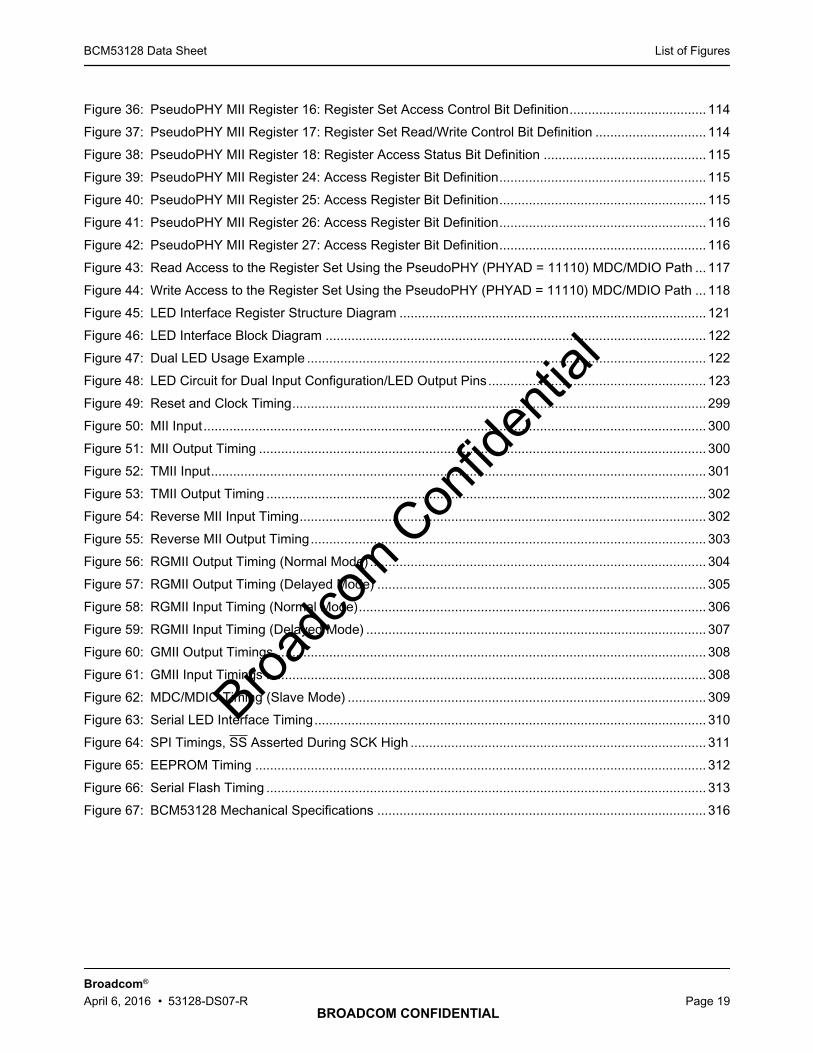
List of FiguresBCM53128 Data Sheet
Broadcom®
April 6, 2016 • 53128-DS07-R Page 19BROADCOM CONFIDENTIAL
Figure 36: PseudoPHY MII Register 16: Register Set Access Control Bit Definition..................................... 114
Figure 37: PseudoPHY MII Register 17: Register Set Read/Write Control Bit Definition .............................. 114
Figure 38: PseudoPHY MII Register 18: Register Access Status Bit Definition ............................................ 115
Figure 39: PseudoPHY MII Register 24: Access Register Bit Definition........................................................ 115
Figure 40: PseudoPHY MII Register 25: Access Register Bit Definition........................................................ 115
Figure 41: PseudoPHY MII Register 26: Access Register Bit Definition........................................................ 116
Figure 42: PseudoPHY MII Register 27: Access Register Bit Definition........................................................ 116
Figure 43: Read Access to the Register Set Using the PseudoPHY (PHYAD = 11110) MDC/MDIO Path ... 117
Figure 44: Write Access to the Register Set Using the PseudoPHY (PHYAD = 11110) MDC/MDIO Path ... 118
Figure 45: LED Interface Register Structure Diagram ................................................................................... 121
Figure 46: LED Interface Block Diagram ....................................................................................................... 122
Figure 47: Dual LED Usage Example ............................................................................................................ 122
Figure 48: LED Circuit for Dual Input Configuration/LED Output Pins........................................................... 123
Figure 49: Reset and Clock Timing................................................................................................................ 299
Figure 50: MII Input........................................................................................................................................ 300
Figure 51: MII Output Timing ......................................................................................................................... 300
Figure 52: TMII Input...................................................................................................................................... 301
Figure 53: TMII Output Timing ....................................................................................................................... 302
Figure 54: Reverse MII Input Timing.............................................................................................................. 302
Figure 55: Reverse MII Output Timing........................................................................................................... 303
Figure 56: RGMII Output Timing (Normal Mode)........................................................................................... 304
Figure 57: RGMII Output Timing (Delayed Mode) ......................................................................................... 305
Figure 58: RGMII Input Timing (Normal Mode).............................................................................................. 306
Figure 59: RGMII Input Timing (Delayed Mode) ............................................................................................ 307
Figure 60: GMII Output Timings..................................................................................................................... 308
Figure 61: GMII Input Timings ....................................................................................................................... 308
Figure 62: MDC/MDIO Timing (Slave Mode) ................................................................................................. 309
Figure 63: Serial LED Interface Timing.......................................................................................................... 310
Figure 64: SPI Timings, SS Asserted During SCK High ................................................................................ 311
Figure 65: EEPROM Timing .......................................................................................................................... 312
Figure 66: Serial Flash Timing ....................................................................................................................... 313
Figure 67: BCM53128 Mechanical Specifications ......................................................................................... 316
Broadc
om C
onfid
entia
l

List of TablesBCM53128 Data Sheet
BROADCOM CONFIDENTIAL
Broadcom®
April 6, 2016 • 53128-DS07-R Page 20
List of Tables
Table 1: TC Decision Tree Summary............................................................................................................... 36
Table 2: Reasons to Forward a Packet to the CPU ......................................................................................... 38
Table 3: Bucket Bit Rate .................................................................................................................................. 47
Table 4: DoS Attacks Detected by BCM53128 ................................................................................................ 51
Table 5: Cable Diagnostic Output .................................................................................................................... 56
Table 6: Unicast Forward Field Definitions ...................................................................................................... 60
Table 7: Address Table Entry for Unicast Address .......................................................................................... 60
Table 8: Multicast Forward Field Definitions .................................................................................................... 61
Table 9: Address Table Entry for Multicast Address........................................................................................ 61
Table 10: Behavior for Reserved Multicast Addresses .................................................................................... 62
Table 11: Flow Control Modes ......................................................................................................................... 70
Table 12: 1000BASE-T External Loopback with External Loopback Plug....................................................... 77
Table 13: 1000BASE-T External Loopback Without External Loopback Plug ................................................. 77
Table 14: 100BASE-TX External Loopback with External Loopback Plug ...................................................... 78
Table 15: 100BASE-TX External Loopback Without External Loopback Plug................................................. 78
Table 16: 10BASE-T External Loopback with External Loopback Plug........................................................... 78
Table 17: 10BASE-T External Loopback Without External Loopback Plug ..................................................... 78
Table 18: Egress Broadcom Tag Format (IMP to CPU) .................................................................................. 81
Table 19: Ingress BRCM Tag (CPU to IMP) .................................................................................................... 82
Table 20: Receive Only Counter (19) Description of Counter.......................................................................... 83
Table 21: Transmit Counters Only (19) Description of Counter ....................................................................... 85
Table 22: Transmit or Receive Counters (10) Description of Counter ............................................................. 86
Table 23: Directly Supported MIB Counters .................................................................................................... 86
Table 24: Indirectly Supported MIB Counters .................................................................................................. 88
Table 25: BCM53128 Supported MIB Extensions ........................................................................................... 89
Table 26: EEPROM_TYPE[1:0] Settings ....................................................................................................... 110
Table 27: EEPROM Header Format .............................................................................................................. 111
Table 28: EEPROM Contents ........................................................................................................................ 111
Table 29: MII Management Frame Format .................................................................................................... 119
Table 30: LED Output Pins Per Port .............................................................................................................. 120
Table 31: I/O Signal Type Definitions ............................................................................................................ 124
Table 32: Signal Type Definitions .................................................................................................................. 125
Table 33: Global Page Register Map............................................................................................................. 142
Table 34: Control Registers (Page 00h) ........................................................................................................ 144
Table 35: Port Traffic Control Register Address Summary............................................................................ 146
Broadc
om C
onfid
entia
l
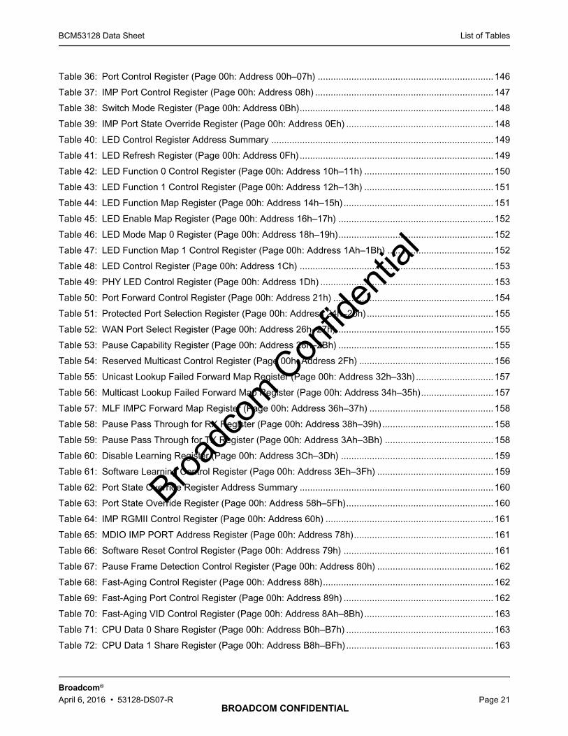
List of TablesBCM53128 Data Sheet
BROADCOM CONFIDENTIAL
Broadcom®
April 6, 2016 • 53128-DS07-R Page 21
Table 36: Port Control Register (Page 00h: Address 00h–07h) .................................................................... 146
Table 37: IMP Port Control Register (Page 00h: Address 08h) ..................................................................... 147
Table 38: Switch Mode Register (Page 00h: Address 0Bh)........................................................................... 148
Table 39: IMP Port State Override Register (Page 00h: Address 0Eh) ......................................................... 148
Table 40: LED Control Register Address Summary ...................................................................................... 149
Table 41: LED Refresh Register (Page 00h: Address 0Fh)........................................................................... 149
Table 42: LED Function 0 Control Register (Page 00h: Address 10h–11h) .................................................. 150
Table 43: LED Function 1 Control Register (Page 00h: Address 12h–13h) .................................................. 151
Table 44: LED Function Map Register (Page 00h: Address 14h–15h).......................................................... 151
Table 45: LED Enable Map Register (Page 00h: Address 16h–17h) ............................................................ 152
Table 46: LED Mode Map 0 Register (Page 00h: Address 18h–19h)............................................................ 152
Table 47: LED Function Map 1 Control Register (Page 00h: Address 1Ah–1Bh) ......................................... 152
Table 48: LED Control Register (Page 00h: Address 1Ch) ........................................................................... 153
Table 49: PHY LED Control Register (Page 00h: Address 1Dh) ................................................................... 153
Table 50: Port Forward Control Register (Page 00h: Address 21h) .............................................................. 154
Table 51: Protected Port Selection Register (Page 00h: Address 24h–25h)................................................. 155
Table 52: WAN Port Select Register (Page 00h: Address 26h–27h)............................................................. 155
Table 53: Pause Capability Register (Page 00h: Address 28h–2Bh) ............................................................ 155
Table 54: Reserved Multicast Control Register (Page 00h: Address 2Fh) .................................................... 156
Table 55: Unicast Lookup Failed Forward Map Register (Page 00h: Address 32h–33h).............................. 157
Table 56: Multicast Lookup Failed Forward Map Register (Page 00h: Address 34h–35h)............................ 157
Table 57: MLF IMPC Forward Map Register (Page 00h: Address 36h–37h) ................................................ 158
Table 58: Pause Pass Through for RX Register (Page 00h: Address 38h–39h)........................................... 158
Table 59: Pause Pass Through for TX Register (Page 00h: Address 3Ah–3Bh) .......................................... 158
Table 60: Disable Learning Register (Page 00h: Address 3Ch–3Dh) ........................................................... 159
Table 61: Software Learning Control Register (Page 00h: Address 3Eh–3Fh) ............................................. 159
Table 62: Port State Override Register Address Summary ........................................................................... 160
Table 63: Port State Override Register (Page 00h: Address 58h–5Fh)......................................................... 160
Table 64: IMP RGMII Control Register (Page 00h: Address 60h) ................................................................. 161
Table 65: MDIO IMP PORT Address Register (Page 00h: Address 78h)...................................................... 161
Table 66: Software Reset Control Register (Page 00h: Address 79h) .......................................................... 161
Table 67: Pause Frame Detection Control Register (Page 00h: Address 80h) ............................................. 162
Table 68: Fast-Aging Control Register (Page 00h: Address 88h).................................................................. 162
Table 69: Fast-Aging Port Control Register (Page 00h: Address 89h) .......................................................... 162
Table 70: Fast-Aging VID Control Register (Page 00h: Address 8Ah–8Bh).................................................. 163
Table 71: CPU Data 0 Share Register (Page 00h: Address B0h–B7h) ......................................................... 163
Table 72: CPU Data 1 Share Register (Page 00h: Address B8h–BFh)......................................................... 163
Broadc
om C
onfid
entia
l
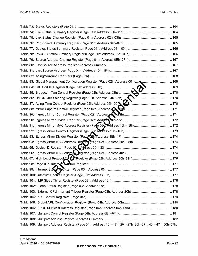
List of TablesBCM53128 Data Sheet
BROADCOM CONFIDENTIAL
Broadcom®
April 6, 2016 • 53128-DS07-R Page 22
Table 73: Status Registers (Page 01h).......................................................................................................... 164
Table 74: Link Status Summary Register (Page 01h: Address 00h–01h) ..................................................... 164
Table 75: Link Status Change Register (Page 01h: Address 02h–03h) ........................................................ 165
Table 76: Port Speed Summary Register (Page 01h: Address 04h–07h) ..................................................... 165
Table 77: Duplex Status Summary Register (Page 01h: Address 08h–09h)................................................. 166
Table 78: PAUSE Status Summary Register (Page 01h: Address 0Ah–0Dh)............................................... 166
Table 79: Source Address Change Register (Page 01h: Address 0Eh–0Fh)................................................ 167
Table 80: Last Source Address Register Address Summary......................................................................... 167
Table 81: Last Source Address (Page 01h: Address 10h–45h)..................................................................... 167
Table 82: Aging/Mirroring Registers (Page 02h)............................................................................................ 168
Table 83: Global Management Configuration Register (Page 02h: Address 00h)......................................... 169
Table 84: IMP Port ID Register (Page 02h: Address 01h) ............................................................................. 169
Table 85: Broadcom Tag Control Register (Page 02h: Address 03h) ........................................................... 170
Table 86: RMON MIB Steering Register (Page 02h: Address 04h–05h)....................................................... 170
Table 87: Aging Time Control Register (Page 02h: Address 06h–09h)......................................................... 170
Table 88: Mirror Capture Control Register (Page 02h: Address 10h–11h).................................................... 171
Table 89: Ingress Mirror Control Register (Page 02h: Address 12h–13h)..................................................... 171
Table 90: Ingress Mirror Divider Register (Page 02h: Address 14h–15h) ..................................................... 172
Table 91: Ingress Mirror MAC Address Register (Page 02h: Address 16h–1Bh).......................................... 172
Table 92: Egress Mirror Control Register (Page 02h: Address 1Ch–1Dh) .................................................... 173
Table 93: Egress Mirror Divider Register (Page 02h: Address 1Eh–1Fh) ..................................................... 174
Table 94: Egress Mirror MAC Address Register (Page 02h: Address 20h–25h) ........................................... 174
Table 95: Device ID Register (Page 02h: Address 30h–33h) ........................................................................ 174
Table 96: Egress Mirror MAC Address Register (Page 02h: Address 40h) ................................................... 174
Table 97: High-Level Protocol Control Register (Page 02h: Address 50h–53h)............................................ 175
Table 98: Page 03h: Interrupt Control Register ............................................................................................. 177
Table 99: Interrupt Status Register (Page 03h: Address 00h) ....................................................................... 177
Table 100: Interrupt Enable Register (Page 03h: Address 08h) .................................................................... 177
Table 101: IMP Sleep Timer Register (Page 03h: Address 10h)................................................................... 178
Table 102: Sleep Status Register (Page 03h: Address 18h) ......................................................................... 178
Table 103: External CPU Interrupt Trigger Register (Page 03h: Address 20h) ............................................. 178
Table 104: ARL Control Registers (Page 04h) .............................................................................................. 179
Table 105: Global ARL Configuration Register (Page 04h: Address 00h)..................................................... 180
Table 106: BPDU Multicast Address Register (Page 04h: Address 04h–09h) .............................................. 180
Table 107: Multiport Control Register (Page 04h: Address 0Eh–0Fh)........................................................... 181
Table 108: Multiport Address Register Address Summary ............................................................................ 182
Table 109: Multiport Address Register (Page 04h: Address 10h–17h, 20h–27h, 30h–37h, 40h–47h, 50h–57h,
Broadc
om C
onfid
entia
l

List of TablesBCM53128 Data Sheet
BROADCOM CONFIDENTIAL
Broadcom®
April 6, 2016 • 53128-DS07-R Page 23
60h–67h)....................................................................................................................................... 182
Table 110: Multiport Vector Register Address Summary............................................................................... 183
Table 111: Multiport Vector Register (Page 04h: Address 18h–1Bh, 28h–2Bh, 38h–3Bh, 48h–4Bh, 58h–5Bh,68h–6Bh) ...................................................................................................................................... 183
Table 112: ARL/VTBL Access Registers (Page 05h) .................................................................................... 184
Table 113: ARL Table Read/Write Control Register (Page 05h: Address 00h) ............................................. 185
Table 114: MAC Address Index Register (Page 05h: Address 02h–07h)...................................................... 185
Table 115: VLAN ID Index Register (Page 05h: Address 08h–09h).............................................................. 186
Table 116: ARL Table MAC/VID Entry N (N=0-3) Register Address Summary............................................. 186
Table 117: ARL Table MAC/VID Entry N (N=0-3) Register (Page 05h: Address 10h–17h, 20h–27h, 30h–37h,40h–47h)....................................................................................................................................... 186
Table 118: ARL Table Data Entry N (N=0-3) Register Address Summary .................................................... 187
Table 119: ARL Table Data Entry N (N=0-3) Register (Page 05h: Address 18h–1Bh, 28h–2Bh, 38h–3Bh, 48h–4Bh) .............................................................................................................................................. 187
Table 120: ARL Table Search Control Register (Page 05h: Address 50h).................................................... 188
Table 121: ARL Search Address Register (Page 05h: Address 51h–52h) .................................................... 189
Table 122: ARL Table Search MAC/VID Result N (N=0-1) Register Address Summary............................... 189
Table 123: ARL Table Search MAC/VID Result N (N=0-1) Register (Page 05h: Address 60h–67h,70h–77h)....................................................................................................................................... 189
Table 124: ARL Table Search Data Result N (N=0-1) Register Address Summary ...................................... 190
Table 125: ARL Table Search Data Result N (N=0-1) Register (Page 05h: Address 68h–6Bh, 78h–7Bh)... 190
Table 126: VLAN Table Read/Write/Clear Control Register (Page 05h: Address 80h) ................................. 191
Table 127: VLAN Table Address Index Register (Page 05h: Address 81h–82h) .......................................... 192
Table 128: VLAN Table Entry Register (Page 05h: Address 83h–86h)......................................................... 192
Table 129: 10/100/1000 PHY Page Summary............................................................................................... 194
Table 130: Register Map (Page 10h–17h)..................................................................................................... 194
Table 131: MII Control Register (Page 10h–17h: Address 00h–01h) ............................................................ 196
Table 132: MII Status Register (Page 10h–17h: Address 02h–03h) ............................................................. 197
Table 133: PHY Identifier Register MSB (Page 10h–17h: Address 04–07h)................................................. 198
Table 134: PHY Identifier Register LSB (Page 10h–17h: Address 06h–07h)................................................ 198
Table 135: Auto-Negotiation Advertisement Register (Page 10h–17h: Address 08h–09h)........................... 199
Table 136: Auto-Negotiation Link Partner Ability Register (Page 10h–17h: Address 0Ah–0Bh) ................... 200
Table 137: Auto-Negotiation Expansion Register (Page 10h–17h: Address 0Ch–0Dh)................................ 201
Table 138: Next Page Transmit Register (Page 10h–17h: Address 0Eh–0Fh) ............................................. 202
Table 139: Link Partner Received Next Page Register (Page 10h–17h: Address 10h–11h) ........................ 203
Table 140: 1000BASE-T Control Register (Page 10h–17h: Address 12h–13h) ............................................ 204
Table 141: 1000BASE-T Status Register (Page 10h–17h: Address 14h–15h) ............................................. 205
Broadc
om C
onfid
entia
l
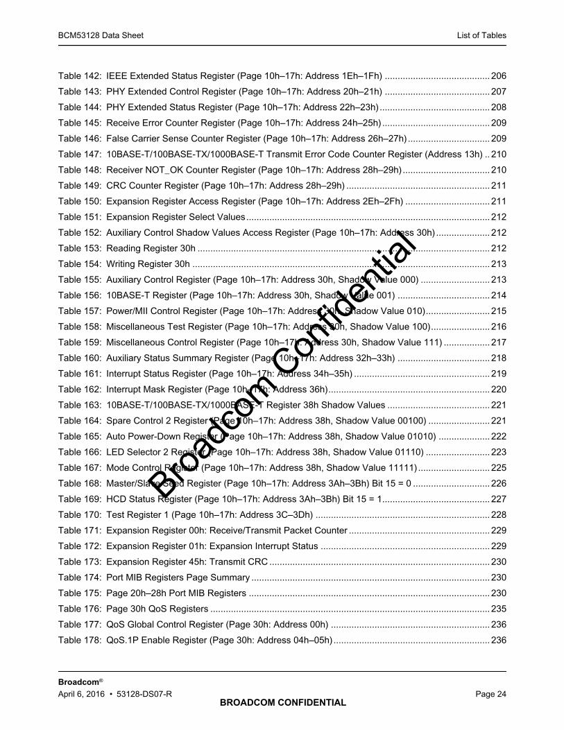
List of TablesBCM53128 Data Sheet
BROADCOM CONFIDENTIAL
Broadcom®
April 6, 2016 • 53128-DS07-R Page 24
Table 142: IEEE Extended Status Register (Page 10h–17h: Address 1Eh–1Fh) ......................................... 206
Table 143: PHY Extended Control Register (Page 10h–17h: Address 20h–21h) ......................................... 207
Table 144: PHY Extended Status Register (Page 10h–17h: Address 22h–23h)........................................... 208
Table 145: Receive Error Counter Register (Page 10h–17h: Address 24h–25h).......................................... 209
Table 146: False Carrier Sense Counter Register (Page 10h–17h: Address 26h–27h)................................ 209
Table 147: 10BASE-T/100BASE-TX/1000BASE-T Transmit Error Code Counter Register (Address 13h) .. 210
Table 148: Receiver NOT_OK Counter Register (Page 10h–17h: Address 28h–29h).................................. 210
Table 149: CRC Counter Register (Page 10h–17h: Address 28h–29h) ........................................................ 211
Table 150: Expansion Register Access Register (Page 10h–17h: Address 2Eh–2Fh) ................................. 211
Table 151: Expansion Register Select Values............................................................................................... 212
Table 152: Auxiliary Control Shadow Values Access Register (Page 10h–17h: Address 30h) ..................... 212
Table 153: Reading Register 30h .................................................................................................................. 212
Table 154: Writing Register 30h .................................................................................................................... 213
Table 155: Auxiliary Control Register (Page 10h–17h: Address 30h, Shadow Value 000) ........................... 213
Table 156: 10BASE-T Register (Page 10h–17h: Address 30h, Shadow Value 001) .................................... 214
Table 157: Power/MII Control Register (Page 10h–17h: Address 30h, Shadow Value 010)......................... 215
Table 158: Miscellaneous Test Register (Page 10h–17h: Address 30h, Shadow Value 100)....................... 216
Table 159: Miscellaneous Control Register (Page 10h–17h: Address 30h, Shadow Value 111) .................. 217
Table 160: Auxiliary Status Summary Register (Page 10h–17h: Address 32h–33h) .................................... 218
Table 161: Interrupt Status Register (Page 10h–17h: Address 34h–35h) ..................................................... 219
Table 162: Interrupt Mask Register (Page 10h–17h: Address 36h)............................................................... 220
Table 163: 10BASE-T/100BASE-TX/1000BASE-T Register 38h Shadow Values ........................................ 221
Table 164: Spare Control 2 Register (Page 10h–17h: Address 38h, Shadow Value 00100) ........................ 221
Table 165: Auto Power-Down Register (Page 10h–17h: Address 38h, Shadow Value 01010) .................... 222
Table 166: LED Selector 2 Register (Page 10h–17h: Address 38h, Shadow Value 01110) ......................... 223
Table 167: Mode Control Register (Page 10h–17h: Address 38h, Shadow Value 11111)............................ 225
Table 168: Master/Slave Seed Register (Page 10h–17h: Address 3Ah–3Bh) Bit 15 = 0 .............................. 226
Table 169: HCD Status Register (Page 10h–17h: Address 3Ah–3Bh) Bit 15 = 1.......................................... 227
Table 170: Test Register 1 (Page 10h–17h: Address 3C–3Dh) .................................................................... 228
Table 171: Expansion Register 00h: Receive/Transmit Packet Counter ....................................................... 229
Table 172: Expansion Register 01h: Expansion Interrupt Status .................................................................. 229
Table 173: Expansion Register 45h: Transmit CRC ...................................................................................... 230
Table 174: Port MIB Registers Page Summary ............................................................................................. 230
Table 175: Page 20h–28h Port MIB Registers .............................................................................................. 230
Table 176: Page 30h QoS Registers ............................................................................................................. 235
Table 177: QoS Global Control Register (Page 30h: Address 00h) .............................................................. 236
Table 178: QoS.1P Enable Register (Page 30h: Address 04h–05h)............................................................. 236
Broadc
om C
onfid
entia
l

List of TablesBCM53128 Data Sheet
BROADCOM CONFIDENTIAL
Broadcom®
April 6, 2016 • 53128-DS07-R Page 25
Table 179: QoS DiffServ Enable Register (Page 30h: Address 06h–07h) .................................................... 237
Table 180: Port N (N=0-7,8) PCP_To_TC Register Address Summary ........................................................ 237
Table 181: Port N (N=0-7,8) PCP_To_TC Register (Page 30h: Address 10h–33h)...................................... 237
Table 182: DiffServ Priority Map 0 Register (Page 30h: Address 40h–45h).................................................. 238
Table 183: DiffServ Priority Map 1 Register (Page 30h: Address 46h–4Bh) ................................................. 239
Table 184: DiffServ Priority Map 2 Register (Page 30h: Address 4Ch–51h) ................................................. 239
Table 185: DiffServ Priority Map 3 Register (Page 30h: Address 52h–57h).................................................. 240
Table 186: TC_To_COS Mapping Register (Page 30h: Address 62h–63h) .................................................. 241
Table 187: CPU_To_COS Map Register (Page 30h: Address 64h–67h) ...................................................... 242
Table 188: TX Queue Control Register (Page 30h: Address 80h)................................................................. 243
Table 189: TX Queue Weight Register Queue[0:3] (Page 30h: Address 81h–84h) ...................................... 243
Table 190: COS4 Service Weight Register (Page 30h: Address 85h–86h)................................................... 244
Table 191: Page 31h VLAN Registers ........................................................................................................... 245
Table 192: Port-Based VLAN Control Register Address Summary ............................................................... 245
Table 193: Port VLAN Control Register (Page 31h: Address 00h–11h) ........................................................ 245
Table 194: Page 32h Trunking Registers ...................................................................................................... 246
Table 195: MAC Trunk Control Register (Page 32h: Address 00h)............................................................... 246
Table 196: Trunk Group 0 Register (Page 32h: Address 10h–11h) .............................................................. 247
Table 197: Trunk Group 1 Register (Page 32h: Address 12h–13h) .............................................................. 247
Table 198: Page 34h IEEE 802.1Q VLAN Registers ..................................................................................... 248
Table 199: Global IEEE 802.1Q Register (Pages 34h: Address 00h) ........................................................... 248
Table 200: Global VLAN Control 1 Register (Page 34h: Address 01h) ......................................................... 250
Table 201: Global VLAN Control 2 Register (Page 34h: Address 02h) ......................................................... 251
Table 202: Global VLAN Control 3 Register (Page 34h: Address 03h–04h) ................................................. 251
Table 203: Global VLAN Control 4 Register (Page 34h: Address 05h) ......................................................... 252
Table 204: Global VLAN Control 5 Register (Page 34h: Address 06h) ......................................................... 253
Table 205: VLAN Multiport Address Control Register (Page 34h: Address 0Ah–0Bh).................................. 254
Table 206: Default IEEE 802.1Q Tag Register Address Summary ............................................................... 255
Table 207: Default IEEE 802.1Q Tag Register (Page 34h: Address 10h–21h) ............................................. 255
Table 208: Double Tagging TPID Register (Page 34h: Address 30h–31h) ................................................... 256
Table 209: ISP Port Selection Portmap Register (Page 34h: Address 32h–33h).......................................... 256
Table 210: DOS Prevent Register ................................................................................................................. 257
Table 211: DOS Control Register (Page 36h: Address 00h–03h) ................................................................. 257
Table 212: Minimum TCP Header Size Register (Page 36h: Address 04h) .................................................. 259
Table 213: Maximum ICMPv4 Size Register (Page 36h: Address 08h-0Bh)................................................. 259
Table 214: Maximum ICMPv6 Size Register (Page 36h: Address 0Ch-0Fh) ................................................ 259
Table 215: DOS Disable Learn Register (Page 36h: Address 08h-0Bh) ....................................................... 259
Broadc
om C
onfid
entia
l
List of TablesBCM53128 Data Sheet
BROADCOM CONFIDENTIAL
Broadcom®
April 6, 2016 • 53128-DS07-R Page 26
Table 216: Page 40h Jumbo Frame Control Register ................................................................................... 260
Table 217: Jumbo Frame Port Mask Registers (Page 40h: Address 01h–04h) ............................................ 260
Table 218: Standard Max Frame Size Registers (Page 40h: Address 05h–06h) .......................................... 261
Table 219: Broadcast Storm Suppression Register (Page 41h) .................................................................... 262
Table 220: Ingress Rate Control Configuration Register (Page 41h: Address 00h–03h) .............................. 262
Table 221: Port Rate Control Register Address Summary ............................................................................ 264
Table 222: Port Rate Control Register (Page 41h: Address 10h–33h).......................................................... 264
Table 223: Port Egress Rate Control Configuration Register Address Summary.......................................... 266
Table 224: Port Egress Rate Control Configuration Registers (Page 41h: Address 80h–91h) ..................... 266
Table 225: IMP Port Egress Rate Control Configuration Register Address Summary .................................. 267
Table 226: IMP Port Egress Rate Control Configuration Registers (Page 41h: Address C0h) ..................... 267
Table 227: Using Rate_Index to Configure Different Egress Rates for IMP in pps ....................................... 268
Table 228: Broadcast Storm Suppression Register (Page 42h) .................................................................... 268
Table 229: EAP Global Control Registers (Page 42h: Address 00h)............................................................. 269
Table 230: EAP Multiport Address Control Register (Page 42h: Address 01h)............................................. 269
Table 231: EAP Destination IP Registers 0 (Page 42h: Address 02h–09h) .................................................. 270
Table 232: EAP Destination IP Registers 1 (Page 42h: Address 0Ah–12h).................................................. 270
Table 233: Port EAP Configuration Register Address Summary................................................................... 271
Table 234: Port EAP Configuration Registers (Page 42h: Address 20h–47h)............................................... 271
Table 235: Broadcast Storm Suppression Register (Page 43h) .................................................................... 272
Table 236: MSPT Control Registers (Page 43h: Address 00h–01h) ............................................................. 272
Table 237: MSPT Aging Control Registers (Page 43h: Address 02h–05h) ................................................... 272
Table 238: MSPT Table Register Address Summary .................................................................................... 273
Table 239: MSPT Table Registers (Page 43h: Address 10h–2Fh)................................................................ 273
Table 240: SPT Multiport Address Bypass Control Register (Page 43h: Address 50h–51h) ........................ 274
Table 241: MIB Snapshot Control Register ................................................................................................... 275
Table 242: MIB Snapshot Control Register (Page 70h: Address 00h) .......................................................... 275
Table 243: Port Snapshot MIB Control Register ............................................................................................ 275
Table 244: Loop Detection Control Register (Page 72h) ............................................................................... 276
Table 245: Loop Detection Control Registers (Page 72h: Address 00h–01h) ............................................... 276
Table 246: Discovery Frame Timer Control Registers (Page 72h: Address 02h) .......................................... 276
Table 247: LED Warning Port Map Registers (Page 72h: Address 03h–04h)............................................... 277
Table 248: Module ID 0 Registers (Page 72h: Address 05h–0Ah) ................................................................ 277
Table 249: Module ID 1 Registers (Page 72h: Address 0Bh–10h) ................................................................ 278
Table 250: Loop Detect Source Address Registers (Page 72h: Address 11h–16h)...................................... 278
Table 251: IMP Port External PHY MII Registers Page Summary ................................................................ 278
Table 252: BroadSync HD Register............................................................................................................... 279
Broadc
om C
onfid
entia
l
List of TablesBCM53128 Data Sheet
BROADCOM CONFIDENTIAL
Broadcom®
April 6, 2016 • 53128-DS07-R Page 27
Table 253: BroadSync HD Enable Control Register (Page 90h: Address 00h–01h) ..................................... 280
Table 254: BroadSync HD Time Stamp Report Control Register (Page 90h: Address 02h) ......................... 280
Table 255: BroadSync HD PCP Value Control Register (Page 90h: Address 03h)....................................... 280
Table 256: BroadSync HD Max Packet Size Register (Page 90h: Address 04h) .......................................... 281
Table 257: BroadSync HD Time Base Register (Page 90h: Address 10h–13h)............................................ 281
Table 258: BroadSync HD Time Base Adjustment Register (Page 90h: Address 14h–17h)......................... 281
Table 259: BroadSync HD Slot Number and Tick Counter Register (Page 90h: Address 18h–1Bh) ............ 282
Table 260: BroadSync HD Slot Adjustment Register (Page 90h: Address 1Ch–1Fh)................................... 282
Table 261: BroadSync HD Class 5 Bandwidth Control Register Address Summary..................................... 283
Table 262: BroadSync HD Class 5 Bandwidth Control Register (Page 90h: Address 30h–31h, 32h–33h, 34h–35h, 36h–37h, 38h–39h)............................................................................................................... 283
Table 263: BroadSync HD Class 4 Bandwidth Control Register Address Summary..................................... 283
Table 264: BroadSync HD Class 4 Bandwidth Control Register (Page 90h: Address 60h–61h, 62h–63h, 64h–65h, 66h–67h, 68h–69h)............................................................................................................... 284
Table 265: BroadSync HD Egress Time Stamp Register Address Summary................................................ 284
Table 266: BroadSync HD Egress Time Stamp Register (Page 90h: Address 90h–93h, 94h–97h, 98h–9Bh,9Ch–9Fh, A0h–A3h, A4h–A7h) .................................................................................................... 284
Table 267: BroadSync HD Egress Time Stamp Status Register (Page 90h: Address D0h) ......................... 284
Table 268: BroadSync HD Link Status Register (Page 90h: Address E0h–E1h) ......................................... 285
Table 269: Traffic Remarking Register .......................................................................................................... 286
Table 270: Traffic Remarking Control Register (Page 91h: Address 00h)..................................................... 286
Table 271: Egress Non-BroadSync HD Packet TC to PCP Mapping Register Address Summary ............... 287
Table 272: Egress Non-BroadSync HD Packet TC to PCP Mapping Register (Page 91h: Address 10h–17h,18h–1Fh, 20h–27h, 28h–2Fh, 30h–37h, 38h–3Fh, 50h-57h)....................................................... 287
Table 273: Page 92h: EEE Control Register ................................................................................................. 288
Table 274: EEE Enable Control Register (Page 92h: Address 00h).............................................................. 288
Table 275: EEE LPI Assert Register (Page 92h: Address 02h)..................................................................... 289
Table 276: EEE LPI Indicate Register (Page 92h: Address 04h) .................................................................. 289
Table 277: EEE RX Idle Symbol Register (Page 92h: Address 06h)............................................................. 289
Table 278: EEE Pipeline Timer Register (Page 92h: Address 0Ch).............................................................. 290
Table 279: EEE Sleep Timer Gig Register (Page 92h: Address 10h) ........................................................... 290
Table 280: EEE Sleep Timer Gig Register (Page 92h: Address 10h) ........................................................... 290
Table 281: EEE Sleep Timer FE Register (Page 92h: Address 34h) ............................................................ 290
Table 282: EEE Sleep Timer FE Register (Page 92h: Address 34h) ............................................................ 291
Table 283: EEE Min LP Timer Gig Register (Page 92h: Address 58h) ......................................................... 291
Table 284: EEE Min LP Timer Gig Register (Page 92h: Address 58h) ......................................................... 291
Table 285: EEE Min LP Timer FE Register (Page 92h: Address 7Ch).......................................................... 291
Broadc
om C
onfid
entia
l
List of TablesBCM53128 Data Sheet
BROADCOM CONFIDENTIAL
Broadcom®
April 6, 2016 • 53128-DS07-R Page 28
Table 286: EEE Min LP Timer FE Register (Page 92h: Address 7Ch).......................................................... 292
Table 287: EEE Wake Timer Gig Register (Page 92h: Address A0h) ........................................................... 292
Table 288: EEE Wake Timer Gig Register (Page 92h: Address A0h) ........................................................... 292
Table 289: EEE Wake Timer FE Register (Page 92h: Address B2h) ............................................................ 292
Table 290: EEE Wake Timer FE Register (Page 92h: Address B2h) ............................................................ 293
Table 291: EEE GLB Congst TH Register (Page 92h: Address C4h) ........................................................... 293
Table 292: EEE TXQ CONG TH Register (Page 92h: Address C6h)............................................................ 293
Table 293: EEE TXQ Cong TH Register (Page 92h: Address C6h) .............................................................. 293
Table 294: Global Registers (Maps to All Pages) ......................................................................................... 295
Table 295: SPI Data I/O Register (Maps to All Registers, Address F0h–F7h) .............................................. 295
Table 296: SPI Status Register (Maps to All Registers, Address FEh) ......................................................... 295
Table 297: Page Register (Maps to All Registers, Address FFh) .................................................................. 296
Table 298: Absolute Maximum Ratings ......................................................................................................... 297
Table 299: Recommended Operating Conditions.......................................................................................... 297
Table 300: Electrical Characteristics.............................................................................................................. 298
Table 301: Reset and Clock Timing............................................................................................................... 299
Table 302: MII Input Timing ........................................................................................................................... 300
Table 303: MII Output Timing ........................................................................................................................ 301
Table 304: TMII Input Timing ......................................................................................................................... 301
Table 305: TMII Output Timing ...................................................................................................................... 302
Table 306: Reverse MII Input Timing............................................................................................................. 302
Table 307: Reverse TMII Input Timing........................................................................................................... 303
Table 308: Reverse MII Output Timing .......................................................................................................... 303
Table 309: Reverse TMII Output Timing........................................................................................................ 303
Table 310: RGMII Output Timing (Normal Mode) .......................................................................................... 304
Table 311: RGMII Output Timing (Delayed Mode) ........................................................................................ 305
Table 312: RGMII Input Timing (Normal Mode)............................................................................................. 306
Table 313: RGMII Input Timing (Delayed Mode) ........................................................................................... 307
Table 314: GMII Output Timing...................................................................................................................... 308
Table 315: GMII Input Timing ........................................................................................................................ 309
Table 316: MDC/MDIO Timing (Slave Mode) ................................................................................................ 309
Table 317: MDC/MDIO Timing (Master Mode) .............................................................................................. 309
Table 318: Serial LED Interface Timing ......................................................................................................... 310
Table 319: SPI Timings.................................................................................................................................. 311
Table 320: EEPROM Timing.......................................................................................................................... 312
Table 321: Serial Flash Timing ...................................................................................................................... 313
Table 322: BCM53128KQLE Package without Heat Sink, 4-Layer Board, P = 3.1W.................................... 314
Broadc
om C
onfid
entia
l

List of TablesBCM53128 Data Sheet
BROADCOM CONFIDENTIAL
Broadcom®
April 6, 2016 • 53128-DS07-R Page 29
Table 323: BCM53128KQLE Package with Heat Sink, 2-Layer Board, P = 3.1W......................................... 314
Table 324: BCM53128IQLE Package with Heat Sink, 4-layer Board, P=3.1W ............................................. 315
Table 325: Ordering Information .................................................................................................................... 317
Broadc
om C
onfid
entia
l

About This Document
Broadcom®
April 6, 2016 • 53128-DS07-R Page 30
BCM53128 Data Sheet
BROADCOM CONFIDENTIAL
About This Document
Purpose and Audience
This document is for designers interested in integrating the BCM53128 switches into their hardware designs andfor others who need specific data about the physical characteristics and operation of the BCM53128 switches.
Acronyms and Abbreviations
In most cases, acronyms and abbreviations are defined on first use.
For a comprehensive list of acronyms and other terms used in Broadcom documents, go to:http://www.broadcom.com/press/glossary.php.
Document Conventions
The following notational conventions are used in this document:
• Signal names are shown in uppercase letters (such as DATA).
• A bar over a signal name indicates that it is active low (such as CE).
• In register and signal descriptions, [n:m] indicates a range from bit n to bit m (such as [7:0] indicates bits 7through 0, inclusive).
• The use of R or Reserved indicates that a bit or a field is reserved by Broadcom for future use. Typically, Ris used for individual bits and Reserved is used for fields.
• Numerical modifiers such as K or M follow traditional usage (for example, 1 KB means 1,024 bytes,100 Mbps [referring to fast Ethernet speed] means 100,000,000 bps, and 133 MHz means 133,000,000Hz).
Broadc
om C
onfid
entia
l

Technical Support
Broadcom®
April 6, 2016 • 53128-DS07-R Page 31
BCM53128 Data Sheet
BROADCOM CONFIDENTIAL
References
The references in this section may be used in conjunction with this document.
For Broadcom documents, replace the “xx” in the document number with the largest number available in therepository to ensure that you have the most current version of the document.
Technical Support
Broadcom provides customer access to a wide range of information, including technical documentation,schematic diagrams, product bill of materials, PCB layout information, and software updates through itscustomer support portal (https://support.broadcom.com). For a CSP account, contact your Sales or Engineeringsupport representative.
In addition, Broadcom provides other product support through its Downloads and Support site(http://www.broadcom.com/support/).
Note: Broadcom provides customer access to technical documentation and software through itsCustomer Support Portal (CSP) and Downloads and Support site (see Technical Support).
Document (or Item) Name Number Source
Broadcom Items
[1] Layout and Design Guide 53128-AN1xx-R CSP
[2] BCM53128 Programmer's Reference Guide 53128-PG1xx-R CSP
Broadc
om C
onfid
entia
l
IntroductionBCM53128 Data Sheet
BROADCOM CONFIDENTIAL
Broadcom®
April 6, 2016 • 53128-DS07-R Page 32
Section 1: Introduction
Overview
The BCM53128 is a single-chip, 9-port Gigabit Ethernet (GbE) switch device. It provides:
• A 9-port nonblocking 10/100/1000-Mbps switch controller
• Eight ports with 10/100/1000BASE-TX-compatible transceivers
• Nine integrated Gigabit MACs (GMACs)
• One GMII/RGMII/MII/RvMII/TMII/RvTMII port for PHY-less connection to the management agent
• An integrated Motorola SPI-compatible interface
• High performance, integrated packet buffer memory
• An address resolution engine
• A set of management information base (MIB) statistics registers
The GMACs support full-duplex and half-duplex modes for 10 Mbps and 100 Mbps and full-duplex for1000 Mbps. Flow control is supported in the half-duplex mode with backpressure. In full-duplex mode, IEEE802.3x frame-based flow control is supported. The GMACs are IEEE 802.3-compliant and support maximumframe sizes of 9720 bytes.
An integrated address management engine provides address learning and recognition functions at maximumframe rates. The address table provides capacity for learning up to 4K unicast addresses. Addresses are addedto the table after receiving an error-free packet.
The MIB statistics registers collect receive and transmit statistics for each port and provide direct hardwaresupport for the Ether-like MIB, MIB II (interfaces), and the first four groups of the RMON MIB. All nine groups ofRMON can be supported by using additional capabilities, such as port mirroring/snooping, together with anexternal microcontroller to process some MIB attributes. The MIB registers can be accessed through the SerialPeripheral Interface Port by an external microcontroller.
Broadc
om C
onfid
entia
l
Features and OperationBCM53128 Data Sheet
BROADCOM CONFIDENTIAL
Broadcom®
April 6, 2016 • 53128-DS07-R Page 33
Section 2: Features and Operation
Overview of Features and Operation
The BCM53128 switches include the following features:
• “Quality of Service” on page 34
• “Port-Based VLAN” on page 38
• “IEEE 802.1Q VLAN” on page 39
• “Programming the VLAN Table” on page 40
• “Double-Tagging” on page 41
• “Jumbo Frame Support” on page 44
• “Port Trunking/Aggregation” on page 44
• “WAN Port” on page 45
• “Rate Control” on page 45
• “Protected Ports” on page 47
• “Port Mirroring” on page 48
• “IGMP Snooping” on page 49
• “MLD Snooping” on page 50
• “IEEE 802.1x Port-Based Security” on page 50
• “DoS Attack Prevention” on page 51
• “MSTP Multiple Spanning Tree” on page 52
• “Software Reset” on page 52
• “Loop Detection” on page 52
• “BroadSync HD” on page 53
• “CableChecker™” on page 56
• “Egress PCP Remarking” on page 57
• “Address Management” on page 57
• “Power Savings Modes” on page 65
The following sections discuss each feature in more detail.
Broadc
om C
onfid
entia
l

Quality of ServiceBCM53128 Data Sheet
BROADCOM CONFIDENTIAL
Broadcom®
April 6, 2016 • 53128-DS07-R Page 34
Quality of Service
The Quality of Service (QoS) feature provides up to six internal queues per port to support six different trafficclasses (TC). The traffic classes can be programmed so that higher-priority TC in the switch experiences lessdelay than lower-priority TC under congested conditions. This can be important in minimizing latency for delay-sensitive traffic. The BCM53128 switches can assign the packet to one of the six egress transmit queuesaccording to information in:
• “Port-Based QoS” on page 35 (ingress port ID)
• “IEEE 802.1p QoS” on page 35
• “MACDA-Based QoS” on page 36
• “TOS/DSCP QoS” on page 36
The “TC Decision Tree” on page 36 decides which priority system is used based on three programmable registerbits detailed in Table 1: “TC Decision Tree Summary,” on page 36. The corresponding traffic class is thenassigned to one of the six queues on a port-by-port basis.
Figure 2: QoS Program Flow
Incoming Packet
TC Decision Tree
Port-Based Traffic Class Mapping
TOS/DSCP Based Traffic Class Mapping
IEEE 802.1p Traffic Class Mapping
MACDA-Based Traffic Class Mapping
COS Mapping
Traffic Class
COS 3
COS 5BroadSync HD
traffic only
COS 4BroadSync HD
traffic only
COS 1
COS 0
COS 2
Outgoing Packet
COS Queue
ID
PCP/DSCP Remarking
SP/W
RR
Alg
orith
m
Broadc
om C
onfid
entia
l
Quality of ServiceBCM53128 Data Sheet
BROADCOM CONFIDENTIAL
Broadcom®
April 6, 2016 • 53128-DS07-R Page 35
Egress Transmit Queues
Each Ethernet egress port has six transmit queues (COS0–COS5). The COS4 and COS5 are dedicated toBroadSync® HD traffic only and can not be shared with other traffic. Each COS queue has its own dedicatedcounter to measure the buffer occupancy of the queue for congestion management purpose. Every Ethernet(ingress) port has its own set of counters to measure the buffer occupancy and the arrival rate related to thetraffic received from the port.
The IMP (egress) port serves four queues (COS0–COS3) and the traffic generated by the Local ManagementPacket Generator which generate management report messages back to CPU, e.g., the Time Sync TX timestamp packets.
Each COS queue has its own dedicated counter to measure the buffer occupancy of the queue for congestionmanagement purpose. The IMP (ingress) port also has its own set of counters to measure the buffer occupancyand the arrival rated to the traffic received from the port, but should be used only if it is configured as a regularEthernet port.
All incoming frames are assigned to an egress transmit queue depending on their assigned TC. Each egresstransmit queue is a list specifying an order for packet transmission. The corresponding egress port transmitspackets from each of the queues according to a programmable algorithm, with the higher TC queues being givengreater access than the lower TC queues. Queue 0 is the lowest-TC queue.
The COS0–COS3 queues are dedicated to non-BroadSync HD traffic only and as programmed in the TX QueueControl register. The BCM53128 uses strict priority (SP) and weighted round robin (WRR) algorithm for COS0–COS3 queues scheduling. The scheduling is configurable using the TX Queue Control register as one offollowing combinations of SP and WRR; 4SP, 4WRR, 1SP and 3WRR, 2SP and 2WRR The WRR algorithmweights for each queue can be programmed using the TX Queue Weight register.
Port-Based QoS
The TC of a packet received from an Ethernet (or IMP) port is assigned with the TC configured for thecorresponding port. The mapping mechanism is globally enabled/disabled by programming the QoS GlobalControl register; the mapping entry is also per-port configured using the Default IEEE 802.1Q Tag register.When disabled, the TC that results from this mapping is 000.
IEEE 802.1p QoS
The TC of a packet received from an Ethernet (or IMP) port is assigned with TC-configured for the correspondingIEEE 802.1p priority code point (PCP). The mapping mechanism is per port enabled/disabled using QoS IEEE802.1p Enable register, the mapping entries are per-port configured by Port N (N = 0–7, 8) PCP_To_TC register.When disabled or if the incoming packet is not tagged, the TC that results from this mapping is 000.
Broadc
om C
onfid
entia
l

Quality of ServiceBCM53128 Data Sheet
BROADCOM CONFIDENTIAL
Broadcom®
April 6, 2016 • 53128-DS07-R Page 36
MACDA-Based QoS
MACDA-Based QoS is enabled when the IEEE 802.1p QoS is disabled using the 802_1P_EN bit in the QoSIEEE 802.1p Enable register. When using MACDA-based QoS, the destination address and VLAN ID is usedto index the ARL table as described in “Address Management” on page 57. The matching ARL entry contains a3-bit TC field as shown in Table 7 on page 60. These bits set the MACDA-based TC for the frame. The MACDA-based TC is assigned to the TC bits depending upon the result shown in Table 1. The TC for the frame ismapped to one of the egress transmit queues base on the ingress port using the TC_To_COS Mapping register.The TC bits for a learned ARL entry default to 0. To change the default, an ARL entry is written to the ARL tableas described in the “Writing an ARL Entry” on page 63. For more information about the egress transmit queues,see “Egress Transmit Queues” on page 35.
TOS/DSCP QoS
The TC of a packet received from an Ethernet (or IMP) port is assigned with TC configured for the correspondingIP TOS/DSCP. The mapping mechanism is per port enabled/disabled using QoS DiffServ Enable register, themapping entries are globally configured by DiffServ Priority Map 0 register through DiffServ Priority Map 3register. When disabled or the incoming packet is not of IPv4/v6 type, the TC resulted from this mapping is 000.
TC Decision Tree
Non-BroadSync HD Frame
The TC decision tree determines which priority system is assigned to TC-mapping bits for the given frame. Assummarized above, the TC bits for the frame can be determined according to the ingress port-based TC, IEEE802.1p TC, MACDA-based TC, DiffServ TC or MACSA-based TC information. The decision on which TCmapping to use is based on the Port_QoS_En bit and the QoS_Layer_Sel bits of the QoS Global Controlregister. Table 1 summarizes how these programmable bits affect the derived TC. The DiffServ and IEEE 802.1pQoS TC are only available if the respective QoS is enabled, and the received packet has the appropriatetagging.
Table 1: TC Decision Tree Summary
Port_QoS_En
QoS_Layer_Sel Value of TC Bits
0 00 IEEE 802.1p TC mapping if available; otherwise, MACDA-based TC mapping.
0 01 DiffServ TC mapping if available; otherwise, TC = 000.
0 10 DiffServ TC mapping for IP frame; otherwise, IEEE 802.1p TC mapping ifavailable; otherwise, MACDA-based TC mapping.
0 11 The highest available TC of the following: IEEE 802.1p TC mapping, DiffServTC mapping, MACDA-based TC mapping or MACSA-based TC mapping.
1 00 MACSA-based TC mapping if available; otherwise, Port-based TC mapping.
1 01 MACSA-based TC mapping if available; otherwise, Port-based TC mapping.
1 10 MACSA-based TC mapping if available; otherwise, Port-based TC mapping.
Broadc
om C
onfid
entia
l
Quality of ServiceBCM53128 Data Sheet
BROADCOM CONFIDENTIAL
Broadcom®
April 6, 2016 • 53128-DS07-R Page 37
BroadSync HD Frame
For the BroadSync HD packet from an Ethernet port, the TC is determined directly from the explicit IEEE802.1Q/P tag carried in the BroadSync HD packets (BroadSync HD packets are expected to always be tagged),which is independent of Table 1 on page 36 TC mapping.
The conditions deciding whether an incoming packet is BroadSync HD are:
1. The port from which the packet is received is configured as BroadSync HD-enabled.
2. The packet received is either VLAN tagged or priority tagged, with PCP = 4 or 5.
3. The MACDA is of multicast type and can be found through ARL table search.
Queuing Class (COS) Determination
The BCM53128 supports the COS mapping through the mapping mechanisms listed below.
• TC to COS mapping: The queuing class to forward a packet to an Ethernet port is mapped from the TCdetermined for the packet. The mapping entries are globally configured using TC_To_COS Mappingregister.
• BroadSync HD to COS mapping: The queuing class to forward a BroadSync HD packet to a BroadSyncHD-enabled Ethernet port is mapped from the PCP carried by the packet. PCP5 is mapped to COS5 andPCP4 is mapped to COS4.
• CPU to COS mapping: The queuing class to forward a packet to the external CPU through the IMP port isdetermined based on the reasons to forward (copy or trap) the packet to CPU. The mapping entries areglobally configured using CPU_To_COS Map register.
Table 2 shows the reasons for forwarding a packet to the CPU. The ToCPU COS values listed are the defaultsetting and are configurable. In order to prevent out of order delivery of the same packet flow to the CPU, theCOS for the mirroring and SA learning reasons must be programmed with a value that is lower than or equal tothe value of the other reasons.
1 11 The highest available TC of the following: Port-based TC mapping, MACSA-based TC mapping, IEEE 802.1p TC mapping, DiffServ TC mapping orMACDA-based TC mapping.
Note: BroadSync HD cannot be received from the IMP port.
Note: When the BCM53128 is configured in the aggregation mode where the IMP operates as theuplink port to the upstream network processor, the COS is decided from the TC based on the normalpacket classification flow. Otherwise, the IMP operates as the interface to the management CPU, andthe COS is decided based on the reasons for forwarding the packet to the CPU.
Table 1: TC Decision Tree Summary (Cont.)
Port_QoS_En
QoS_Layer_Sel Value of TC Bits
Broadc
om C
onfid
entia
l
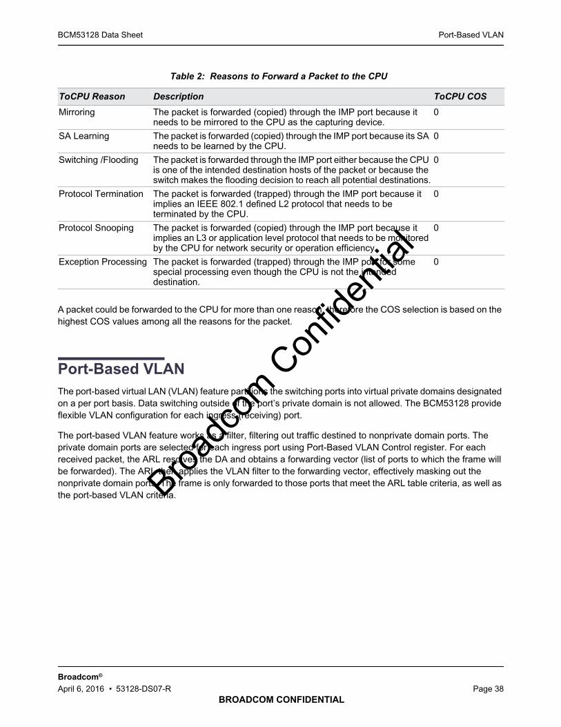
Port-Based VLANBCM53128 Data Sheet
BROADCOM CONFIDENTIAL
Broadcom®
April 6, 2016 • 53128-DS07-R Page 38
A packet could be forwarded to the CPU for more than one reason, therefore the COS selection is based on thehighest COS values among all the reasons for the packet.
Port-Based VLAN
The port-based virtual LAN (VLAN) feature partitions the switching ports into virtual private domains designatedon a per port basis. Data switching outside of the port’s private domain is not allowed. The BCM53128 provideflexible VLAN configuration for each ingress (receiving) port.
The port-based VLAN feature works as a filter, filtering out traffic destined to nonprivate domain ports. Theprivate domain ports are selected for each ingress port using Port-Based VLAN Control register. For eachreceived packet, the ARL resolves the DA and obtains a forwarding vector (list of ports to which the frame willbe forwarded). The ARL then applies the VLAN filter to the forwarding vector, effectively masking out thenonprivate domain ports. The frame is only forwarded to those ports that meet the ARL table criteria, as well asthe port-based VLAN criteria.
Table 2: Reasons to Forward a Packet to the CPU
ToCPU Reason Description ToCPU COS
Mirroring The packet is forwarded (copied) through the IMP port because itneeds to be mirrored to the CPU as the capturing device.
0
SA Learning The packet is forwarded (copied) through the IMP port because its SAneeds to be learned by the CPU.
0
Switching /Flooding The packet is forwarded through the IMP port either because the CPUis one of the intended destination hosts of the packet or because theswitch makes the flooding decision to reach all potential destinations.
0
Protocol Termination The packet is forwarded (trapped) through the IMP port because itimplies an IEEE 802.1 defined L2 protocol that needs to beterminated by the CPU.
0
Protocol Snooping The packet is forwarded (copied) through the IMP port because itimplies an L3 or application level protocol that needs to be monitoredby the CPU for network security or operation efficiency.
0
Exception Processing The packet is forwarded (trapped) through the IMP port for somespecial processing even though the CPU is not the intendeddestination.
0
Broadc
om C
onfid
entia
l
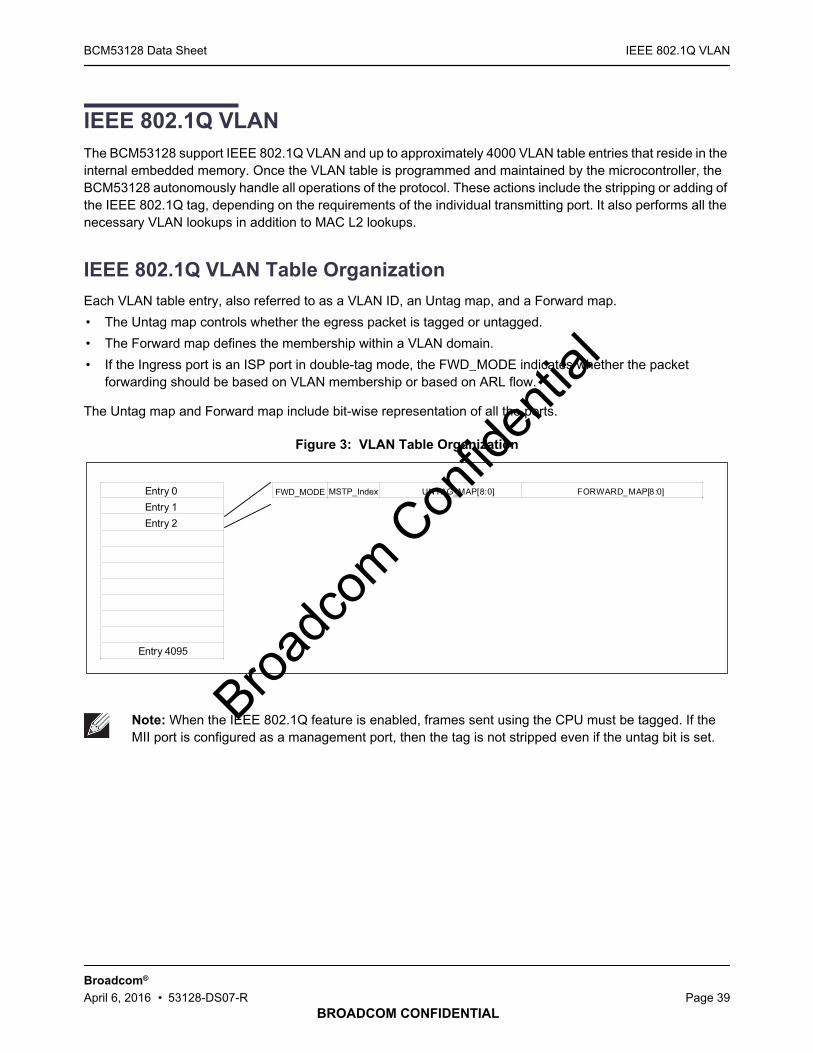
IEEE 802.1Q VLANBCM53128 Data Sheet
BROADCOM CONFIDENTIAL
Broadcom®
April 6, 2016 • 53128-DS07-R Page 39
IEEE 802.1Q VLAN
The BCM53128 support IEEE 802.1Q VLAN and up to approximately 4000 VLAN table entries that reside in theinternal embedded memory. Once the VLAN table is programmed and maintained by the microcontroller, theBCM53128 autonomously handle all operations of the protocol. These actions include the stripping or adding ofthe IEEE 802.1Q tag, depending on the requirements of the individual transmitting port. It also performs all thenecessary VLAN lookups in addition to MAC L2 lookups.
IEEE 802.1Q VLAN Table Organization
Each VLAN table entry, also referred to as a VLAN ID, an Untag map, and a Forward map.
• The Untag map controls whether the egress packet is tagged or untagged.
• The Forward map defines the membership within a VLAN domain.
• If the Ingress port is an ISP port in double-tag mode, the FWD_MODE indicates whether the packetforwarding should be based on VLAN membership or based on ARL flow.
The Untag map and Forward map include bit-wise representation of all the ports.
Figure 3: VLAN Table Organization
Note: When the IEEE 802.1Q feature is enabled, frames sent using the CPU must be tagged. If theMII port is configured as a management port, then the tag is not stripped even if the untag bit is set.
Entry 0 MSTP_Index UNTAG_MAP[8:0] FORWARD_MAP[8:0]
Entry 1Entry 2
Entry 4095
FWD_MODE
Broadc
om C
onfid
entia
l

Programming the VLAN TableBCM53128 Data Sheet
BROADCOM CONFIDENTIAL
Broadcom®
April 6, 2016 • 53128-DS07-R Page 40
Programming the VLAN Table
The IEEE 802.1Q VLAN feature can be enabled by writing to the Enable IEEE 802.1Q bit in the Global IEEE802.1Q register. The default priority and VID can be assigned to each port in the Default IEEE 802.1Q Tagregister. These are necessary when tagging a previously untagged frame. The Hashing algorithm uses either[VID, MAC] or [MAC] for the ARL index key, depending on the VLAN Learning Mode bits in the Global IEEE802.1Q register. If both the VID and MAC address are used, a single MAC address is able to be a member ofmultiple VLANs simultaneously.
The VLAN table can be written using the following steps:
1. Use the VLAN Table Entry register to define the ports that are part of the VLAN group and the ports thatshould be untagged.
2. Use the VLAN Table Address Index register to define the VLAN ID of the VLAN group.
3. Set bit [1:0] = 00 of the VLAN Table Read/Write/Clear Control register to indicate a write operation.
4. Set bit 7 of the VLAN Table Read/Write/Clear Control register to 1, starting the write operation. This bitreturns to 0 when the write is complete.
The VLAN table can be read using the following steps:
1. Use the VLAN Table Address Index register to define from which VLAN group to read the data.
2. Set bit [1:0] = 01 of the VLAN Table Read/Write/Clear Control register to indicate a read operation.
3. Set bit 7 of the VLAN Table Read/Write/Clear Control register to 1 to start the read operation. This bit returnsto 0 when the read is complete.
4. Read the VLAN Table Entry register to obtain the VLAN table entry information.
Note: VLAN ID 0xFFF is reserved. However VID = 0xFFF can be forwarded if the VID_FFF_Fwdingbit is set in the Global VLAN Control 5 register.
Broadc
om C
onfid
entia
l

Double-TaggingBCM53128 Data Sheet
BROADCOM CONFIDENTIAL
Broadcom®
April 6, 2016 • 53128-DS07-R Page 41
Double-Tagging
The BCM53128 provide the double tagging feature, which is useful for ISP applications. When the ISPaggregates incoming traffic from each individual customer, the extra tag (double tag) can provide an additionallayer of tagging to the existing IEEE 802.1Q VLAN. The ISP tag (extra tag) is a way of separating individualcustomers from other customers. Using the IEEE 802.1Q VLAN tag, the individual customer’s traffic can beseparated.
When the double-tagging feature is enabled using the Global VLAN Control 4 register and the Enable IEEE802.1Q (bit7) of the Global IEEE 802.1Q register, users can expect two VLAN tags in a frame: the tag close toMAC_SA is the ISP tag, and the one following is the customer tag as shown in Figure 4.
Figure 4: ISP Tag Diagram
The switch uses the ISP tag for ARL and VLAN table accesses and the customer tag as an IEEE 802.1Q tag.There is a per chip programmable register Double Tagging TPID register for ISP tag (default = 9100'h). All ISPtags will be qualified by this Tag Protocol ID (TPID) value.
When the double-tagging feature is enabled, all switch ports are separated into two groups, ISP ports andcustomer ports. The BCM53128 performs the normalization process for all ingress frames, whether from the ISPport or customer port. The normalization process is to insert an ISP tag, customer tag, or ISP + customer tag(depending whether the ingress frame is without tags or with one tag) to allow all ingress frames with a doubletag. But if the ingress frames are with a double tag (ISP + customer tag), and the ISP tag TPID matches theTPID specified in the Double Tagging TPID register, it does not perform the normalization process. The ISP portsare defined in the ISP Port Selection Portmap register. When the port (s) corresponding bit(s) are set, that port(s) should be connected ISP, and otherwise connected to customers. Each switch device can have multiple portsassigned as ISP ports, and each ISP is uniquely identified using different VLAN forward maps or the port-basedVLAN feature.
If the ingress frame is an untagged frame, the IEEE 802.1Q tag which can be configured by the Default IEEE802.1Q Tag Register (Page 34h: Address 10h) will add to an incoming untagged frame. If the ingress frame istagged with the 802.1p tag, the default VID which can be configured by the Default IEEE 802.1Q Tag Register(Page 34h: Address 10h) will be tagged the incoming 802.1p frame.
MAC_DA MAC_SA ISP_TAG Customer_tag Ty/Len Payload
TPID VID
Broadc
om C
onfid
entia
l
Double-TaggingBCM53128 Data Sheet
BROADCOM CONFIDENTIAL
Broadcom®
April 6, 2016 • 53128-DS07-R Page 42
ISP Port
It is possible for ISP port to receive three different types of frames: untagged, ISP-tagged, and ISP+Customer-tagged frames.
When the double-tagging feature is enabled and the received frame is untagged (or the TPID does not matchwith ISP TPID specified in Double Tagging TPID register, the default ISP tag and customer tag are added, andVLAN ID of ISP tag receives it from the port default VID. The frames are forwarded according to the VLAN table.However, if the Port-Based VLAN Control register is enabled, the egress ports specified in the port-VLAN controlregister override the VLAN table settings. If the received frame is ISP tagged (TPID matches with the ISP tagVLAN ID specified in the double-tagging TPID register), the default customer tag (8100 + default PVID) is added,the ISP VID is used to access the ARL table, and the ISP tag can be stripped on the way out according to theuntagged bit setting in the VLAN table. In addition, ISP port frame can forward to the destination port directlybased on forward port map of VLAN table by setting FWD_MODE bit to 1 of VLAN Table Entry register.
The VLAN ID is generated from the ISP tag, and TC is generated from the ingress frame outer tag.
Customer Port
It is also possible for Customer port to receive two different types of frames: untagged and Customer-taggedframes.
When the double-tagging feature is enabled, all the ingress frames preform the normalization process to inserta ISP tag or ISP + Customer tag (depending whether the ingress frame is without tags or with one tag) to allowall ingress frames with a double tag. The VLAN ID of ISP tag receives it from the port default VID.
The VLAN ID is generated from the ISP tag, and the TC is generated from the ingress frame outer tag.
There are two possible traffic scenarios; one from a customer port to an ISP port, and one from an ISP port toa customer port.
Note: It is illegal to strip out the ISP tag on the ISP egress port by using the untagged bit setting inthe VLAN table.
Only the VLAN tagged or untagged packets are expected for the ingress of the customer ports. Thecustomer do not add the ISP tags.
Broadc
om C
onfid
entia
l

Double-TaggingBCM53128 Data Sheet
BROADCOM CONFIDENTIAL
Broadcom®
April 6, 2016 • 53128-DS07-R Page 43
Uplink Traffic (from Customer Port to ISP)
Data traffic is traffic received from the customer port without tags or a customer tag, and the frame is destinedfor an ISP port. The customer ingress port performs a normalization process to allow ingress frames with doubletags (ISP + Customer tag), and the ISP tag VID is based on the port default VID tag.
However, if the ingress frame is with an 802.1p tag, the VID of 802.1p tag is changed by the VID of port defaultVID tag after the customer port normalization process. The TC do not change.
Control traffic frames can be forwarded to the CPU first and then the CPU forwards to the ISP port if the switchmanagement mode is enabled and if the RESV_MCAST_FLOOD bit=0 in the Global VLAN Control 4 register.In this case, the control frame adds an ISP tag by ingress port and forward to the CPU. The CPU can thenforward it to the ISP port with or without the ISP tag by using the egress-direct feature.
Downlink Traffic (from ISP to Customer Port)
Data traffic frame received from ISP port may or may not have ISP tag attached. When the received frame doesnot have an ISP tag and customer tag, the ISP ingress port does a normalization process to insert double tags(ISP + Customer tag), and the ISP tag VID is based on the port default VID tag. All ARL and VID table accessshould be based on the new tag. The traffic is then forwarded to the customer port through proper VLANconfiguration. Usually, the software configures so the customer Egress port continuously removes the ISP tag.However, it is based on how the untagged map is configured.
Moreover, if the ingress frame is with an 802.1p tag, the VID of 802.1p tag is changed by the VID of port defaultVID tag after the ISP port normalization process. The TC will not change.
The Control traffic is forwarded to the CPU when the switch management mode is enable and if theRESV_MCAST_FLOOD bit=0 in the Global VLAN Control 4 register. The BCM53128 can also support multipleISP port configurations by enabled the FWD_MODE bit of VLAN Table Entry register. There are also two waysto separate traffic that belongs to two different ISP customers:
1. Each group (ISP, and customer) is assigned to the same VLAN group, so that traffic does not leak to otherISP.
2. Use the Port-based VLAN to separate traffic that belongs to a different ISP.
Broadc
om C
onfid
entia
l

Jumbo Frame SupportBCM53128 Data Sheet
BROADCOM CONFIDENTIAL
Broadcom®
April 6, 2016 • 53128-DS07-R Page 44
Jumbo Frame Support
The BCM53128 can receive and transmit frames of extended length on ports linked at gigabit speed. Referredto as jumbo frames, these packets are longer than standard maximum size which is defined using the StandardMax Frame Size register, but shorter than 9720 bytes. Jumbo packets can only be received or forwarded to1000BASE-T linked ports that are jumbo-frame enabled. Up to 38 buffer memory pages are required for storingthe longest allowed jumbo frame. While there is no physical limitation to the number of ports that can be jumboenabled, it is recommended that no more than two be enabled simultaneously to ensure system performance.There is no performance penalty for enabling additional jumbo ports beyond the potential strain on memoryresources that can occur due to accumulated jumbo packets at multiple ports.
Port Trunking/Aggregation
The BCM53128 support MAC-based trunking. The trunking feature allows up to four ports to be groupedtogether as a single-link connection between two switch devices. This increases the effective bandwidth througha link and provides redundancy. The BCM53128 allow up to two trunk groups. Trunks are composed ofpredetermined ports and can be enabled using Trunking Group 0 register. Ports within a trunk group must be ofthe same linked speed. By performing a dynamic hashing algorithm on the MAC address, each packet destinedfor the trunk is forwarded to one of the valid ports within the trunk group. This method has several keyadvantages. By dynamically performing this function, the traffic patterns can be more balanced across the portswithin a trunk. In addition, the MAC-based algorithm provides dynamic failover. If a port within a trunking groupfails, the other port within the trunk automatically assumes all traffic designated for the trunk. It allows for aseamless, automatic redundancy scheme. This hashing function can be performed on either the DA, SA, or DA/SA, depending on the Trunk Hash Selector bit of MAC Trunking Control register.
Figure 5: Trunking
Port X
Port Y
Port Z
Port 0
Port 1
Port 2
One Pipe
Switch 1 Switch 2
Frame XFrame YFrame Z
Broadc
om C
onfid
entia
l
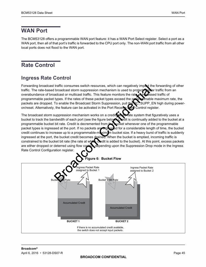
WAN PortBCM53128 Data Sheet
BROADCOM CONFIDENTIAL
Broadcom®
April 6, 2016 • 53128-DS07-R Page 45
WAN Port
The BCM53128 offers a programmable WAN port feature: it has a WAN Port Select register. Select a port as aWAN port, then all of that port’s traffic is forwarded to the CPU port only. The non-WAN port traffic from all otherlocal ports does not flood to the WAN port.
Rate Control
Ingress Rate Control
Forwarding broadcast traffic consumes switch resources, which can negatively impact the forwarding of othertraffic. The rate-based broadcast storm suppression mechanism is used to protect regular traffic from anoverabundance of broadcast or multicast traffic. This feature monitors the rate of ingressed traffic ofprogrammable packet types. If the rates of these packet types exceed the programmable maximum rate, thepackets are dropped. To enable the Broadcast Storm Suppression, pull the BC_SUPP_EN high during power-on/reset. Alternatively, the feature can be activated in the Port Receive Rate Control register.
The broadcast storm suppression mechanism works on a credit-based rate system that figuratively uses abucket to track the bandwidth of each port (see the figure below). Credit is continually added to the bucket at aprogrammable bucket bit rate. Credit is decremented from the bucket whenever one of the programmablepacket types is ingressed at the port. If no packets are ingressed for a considerable length of time, the bucketcredit continues to increase up to a programmable-maximum bucket size. If a heavy burst of traffic is suddenlyingressed at the port, the bucket credit becomes drained. When the bucket is emptied, incoming traffic isconstrained to the bucket bit rate (the rate at which credit is added to the bucket). At this point, excess packetsare either dropped or deterred using flow control, depending upon the Suppression Drop mode in the IngressRate Control Configuration register.
Figure 6: Bucket Flow
Accumulated Credit
BUCKET 1 BUCKET 2
Accumulated Credit
Bucket 2 Bit Rate
Ingress Packet Rate assigned to Bucket 2
If there is no accumulated credit available, the switch does not accept input packets .
Ingress Packet Rate assigned to Bucket 1
Bucket 1 Bit RateBroadc
om C
onfid
entia
l
Rate ControlBCM53128 Data Sheet
BROADCOM CONFIDENTIAL
Broadcom®
April 6, 2016 • 53128-DS07-R Page 46
Two-Bucket System
For added flexibility, the BCM53128 employ two buckets to track the rate of ingressed packets. Each of the twobuckets (Bucket 0 and Bucket 1) can be programmed to monitor different packet types. For example, Bucket 0could monitor broadcast packets, while Bucket 1 monitors multicast packets. Multiple packet types can bemonitored by each bucket, and a packet type can be monitored by both buckets.
The rates of each bucket can be individually programmed (see “Bucket Bit Rate”). For example, the broadcastpackets of Bucket 0 could have a maximum rate of 3 Mbps, whereas the multicast packets of Bucket 1 could beallowed up to 80 Mbps. The size of each bucket can be programmed using the Suppressed Packet Type Maskof the Ingress Rate Control Configuration register. This determines the maximum credit than can accumulate ineach bucket. The Rate Count and Bucket Size can be individually programmed for each port, providing anotherlevel of flexibility. Suppression control can be enabled or disabled on a per-port basis Ingress Rate ControlConfiguration register. This system allows the user to control dual packet-type rates on a per-port basis.
Egress Rate Control
The BCM53128 monitor the rate of egress traffic per port. Unlike the Ingress traffic rate control, the Egress RateControl provides only the per port rate control regardless of traffic types. This feature only uses one bucket totrack the rate of egressed packets. The Egress Rate Control feature can be enabled in the Port Egress RateControl Configuration register and the output rate per port can be controlled by setting the bucket size andRefresh Count in the same register. The Egress Rate Control feature only support absolute bit rate mode (BitRate Mode = 0) and the bucket bit rate calculation is shown in Table 3.
Broadc
om C
onfid
entia
l

Protected PortsBCM53128 Data Sheet
BROADCOM CONFIDENTIAL
Broadcom®
April 6, 2016 • 53128-DS07-R Page 47
Bucket Bit Rate
The relative ingress rates of each bucket can be programmed Port Receive Rate Control register on a per portbasis. Each port has a programmable Rate Count value for Bucket 0 and Bucket 1. Additionally, the bit ratemode is programmed Ingress Rate Control Configuration register on a chip basis. If this bit is 1, the packet rateis automatically scaled according to the port link speed. Ports operating at 1000 Mbps would be allotted a 100times higher ingress rate than ports linked at 10 Mbps. Together, the Rate Count value and the bit rate modedetermine the bucket bit rate, which is a reflection of how quickly data can be ingressed (Kbps) at the given portfor a given bucket. The Rate Count values are specified in the following table. Values outside these ranges arenot valid entries.
IMP Port Egress Rate Control
The IMP port egress is configurable of rate limiting at packet-per-second (PPS) granularity, in addition to bits-per-second (BPS) granularity. It can be configured using the IMP Port Egress Rate Control Configurationregister.
Protected Ports
The Protected Ports feature allows certain ports to be designated as protected Protected Port Selection register.All other ports are unprotected. Traffic between protected port group members is blocked. However, protectedports are able to send traffic to unprotected ports. Unprotected ports can send traffic to any port. Severalapplications that can benefit from protected ports:
• Aggregator: For example, all the available ports are designated as protected ports except a singleaggregator port. No traffic incoming to the protected ports is sent within the protected ports group. Anyflooded traffic is forwarded only to the aggregator port.
• To prevent nonsecured ports from monitoring important information on a server port, the server port andnonsecured ports are designated as protected. The nonsecured ports will not be able to receive traffic fromthe server port.
Table 3: Bucket Bit Rate
Rate Count (RC)Bit RateMode Link Speed
Bucket Bit RateEquation
Approximate ComputedBucket Bit RateValues (As a function of RC)
1–28 0 Any = (RC x 8 x 1M) / 125 64 KB, 128 KB, 192 KB,..., 1.792 MB
29–127 0 Any = (RC – 27) x 1M 2 MB, 3 MB, 4 MB,..., 100 MB
128–240 0 Any = (RC – 115) x 1M x 8 104 MB, 112 MB, 120 MB,..., 1000 MB
1–125 1 10 Mbps = (RC x 8 x 1M) / 100 0.08 MB, 0.16 MB, 0.24 MB,... 10 MB
1–125 1 100 Mbps = (RC x 8 x 1M) / 10 0.8 MB, 1.6 MB, 2.4 MB,..., 100 MB
1–125 1 200 Mbps = (RC x 8 x 1M) / 5 1.6 MB, 3.2 MB, 4.8 MB,..., 200 MB
1–125 1 1000 Mbps = RC x 8 x 1M 8 MB, 16 MB, 24 MB,... 1000 MB
Note: 1M represents 1 x 10⁶.
Broadc
om C
onfid
entia
l
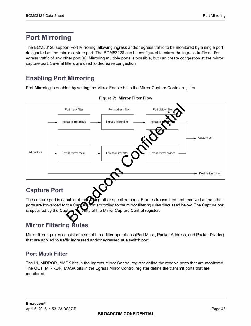
Port MirroringBCM53128 Data Sheet
BROADCOM CONFIDENTIAL
Broadcom®
April 6, 2016 • 53128-DS07-R Page 48
Port Mirroring
The BCM53128 support Port Mirroring, allowing ingress and/or egress traffic to be monitored by a single portdesignated as the mirror capture port. The BCM53128 can be configured to mirror the ingress traffic and/oregress traffic of any other port (s). Mirroring multiple ports is possible, but can create congestion at the mirrorcapture port. Several filters are used to decrease congestion.
Enabling Port Mirroring
Port Mirroring is enabled by setting the Mirror Enable bit in the Mirror Capture Control register.
Figure 7: Mirror Filter Flow
Capture Port
The capture port is capable of monitoring other specified ports. Frames transmitted and received at the otherports are forwarded to the Capture port according to the mirror filtering rules discussed below. The Capture portis specified by the Capture Port bits of the Mirror Capture Control register.
Mirror Filtering Rules
Mirror filtering rules consist of a set of three filter operations (Port Mask, Packet Address, and Packet Divider)that are applied to traffic ingressed and/or egressed at a switch port.
Port Mask Filter
The IN_MIRROR_MASK bits in the Ingress Mirror Control register define the receive ports that are monitored.The OUT_MIRROR_MASK bits in the Egress Mirror Control register define the transmit ports that aremonitored.
All packets
Port mask filter
Ingress mirror mask
Port address filter
Ingress mirror filter
Port divider filter
Ingress mirror divider
Egress mirror mask Egress mirror filter Egress mirror divider
Capture port
Destination port(s)
Broadc
om C
onfid
entia
l

IGMP SnoopingBCM53128 Data Sheet
BROADCOM CONFIDENTIAL
Broadcom®
April 6, 2016 • 53128-DS07-R Page 49
Any number of ingress/egress ports can be programmed to be mirrored, but bandwidth restrictions on the one-mirror capture port should be taken into account to avoid congestion or packet loss.
Packet Address Filter
The Ingress Mirror Control register is used to set the type of filtering that is applied to frames received on themirrored ports. The IN_MIRROR_FILTER bits select among the following:
• Mirror all received frames
• Mirror received frames with DA = x
• Mirror received frames with SA = x
where x is the 48-bit MAC address programmed into the Ingress Mirror MAC Address register. Likewise, theEgress Mirror Control register is used to set the type of filtering that is applied to frames transmitted on theegressed mirrored ports. The filtering MAC address is specified in the Egress Mirror MAC Address register.
Packet Divider Filter
The IN_DIV_EN bit in the Ingress Mirror Control register allows further statistical sampling. When IN_DIV_EN= 1, the receive frames passing the initial filter are divided by the value IN_MIRROR_DIV, which is a 10-bit valuestored in the Ingress Mirror Divider register. Only one out of every n frames is forwarded to the mirror captureport, where n = IN_MIRROR_DIV +1. This allows the following additional capabilities:
• Mirror every nth received frame
• Mirror every nth received frame with DA = x
• Mirror every nth received frame with SA = x
Similarly, the Egress Mirror Divide function is controlled by the Egress Mirror Control register and the EgressMirror Divider register.
IGMP Snooping
The BCM53128 supports IP layer IGMP Snooping which includes IGMP unknown, query, report, and leavemessages using the High-Level Protocol Control register.
A frame with a value of 2 in the IP header protocol field and IGMP frames are forwarded to the CPU port. Themanagement CPU can then determine, from the IGMP control packets which port should participate in themultigroup session. The management CPU proactively programs the multicast address in the ARL table or themultiport address entries. If the IGMP_FWD_EN in the High-Level Protocol Control register is enabled, IGMPframes will be trapped to the CPU port only.
Note: When multiple ingress ports have been enabled in the IN_MIRROR_MASK, the cumulative totalpacket count received from all ingress ports is divided by the value of IN_MIRROR_DIV to deliver thenth receive frame to the mirror capture port. Egressed frames are governed by theOUT_MIRROR_MASK bit and the OUT_MIRROR_DIV bit.
Broadc
om C
onfid
entia
l
MLD SnoopingBCM53128 Data Sheet
BROADCOM CONFIDENTIAL
Broadcom®
April 6, 2016 • 53128-DS07-R Page 50
MLD Snooping
The BCM53128 supports IP layer MLD Snooping including MLD query, report, and done messages using theHigh-Level Protocol Control register.
IEEE 802.1x Port-Based Security
IEEE 802.1x is a port-based authentication protocol. By receiving and extracting special frames, the CPU cancontrol whether the ingress and egress ports should forward packets or not. If a user port wants service fromanother port (authenticator), it must get approved by the authenticator. EAPOL is the protocol used by theauthentication process. The BCM53128 detect EAPOL frames by checking the destination address of the frame.The Destination addresses should be either a multicast address as defined in IEEE 802.1x (01-80-C2-00-00-03) or a user-predefined MAC (unicast or multicast) address. Once EAPOL frames are detected, the frames areforwarded to the CPU so it can send the frames to the authenticator server. Eventually, the CPU determineswhether the requestor is qualified or not based on its MAC_Source addresses, and frames are either acceptedor dropped. The per-port EAP can be programmed in the register.
BCM53128 provides three modes for implementing the IEEE 802.1x feature. Each mode can be selected bysetting the appropriate bits in the register.
The Basic Mode (when EAP Mode = 00'b) is the standard mode, the EAP_BLK_MODE bit would be set beforeauthentication to block all of the incoming packets, upon authentication, the EAP_BLK_MODE bit would becleared to allow all the incoming packets. In this mode, the Source Address of incoming packets is not checked.
The second mode is Extended Mode (when EAP Mode = 10'b), where an extra filtering mechanism isimplemented after the port is authenticated. If the Source MAC address is unknown, the incoming packets wouldbe dropped and the unknown SA would not be learned. However if the incoming packet is IEEE 802.1x packet,or special frames, the incoming packets will be forwarded. The definition of the Unknown SA in this case is whenthe switch cannot match the incoming Source MAC address to any of the addresses in ARL table, or theincoming Source MAC address matches the address in ARL table, but the port number is mismatched. The thirdmode is Simplified Mode (when EAP Mode = 11'b). In this mode, the unknown Source MAC address packetswould be forwarded to CPU rather than dropped. Otherwise, it is same as the Extended Mode operation.
Note: The BCM53128 checks only the destination addresses to qualify EAPOL frames. Ethernet typefields, packet type fields, or non-IEEE 802.1Q frames are not checked.
Broadc
om C
onfid
entia
l

DoS Attack PreventionBCM53128 Data Sheet
BROADCOM CONFIDENTIAL
Broadcom®
April 6, 2016 • 53128-DS07-R Page 51
DoS Attack Prevention
The BCM53128 supports the detection of the following DoS (Denial of Service) attack types based on a registersetting, which can be programmed to drop or not to drop each type of DoS packet, respectively.
• MIN_TCP_Header_Size is programmable between 0 and 255 bytes, inclusive. The default value is set to20 bytes (TCP header without options).
• MAX_ICMPv4_Size is programmable between 0 and 9.6 KB, inclusive. The default value is set to 512bytes.
• MIN_TCP_Header_Size is programmable between 0 and 9.6 KB, inclusive. The default value is set to 512bytes.
• The default control setting for all types of DoS attacks is not to drop the DoS attack packet.
• It is globally configurable whether to perform the SA learning operation with the received packets of theDoS attack type defined in the registers, regardless of the individual DoS attack types.
• Once a packet is detected as a DoS attack type that must be dropped, the packet is dropped regardless ofARL forwarding decisions, but its forwarding based on mirroring function is not affected.
Table 4: DoS Attacks Detected by BCM53128
DoS Attack Type Description
IP_LAND IPDA = IPSA in an IPv4/IPv6 datagram
TCP_BLAT DPort = SPort in a TCP header carried in an unfragmented IP datagram or in the firstfragment of a fragmented IP datagram
UDP_BLAT DPort = SPort in a UDP header carried in an unfragmented IP datagram or in the firstfragment of a fragmented IP datagram
TCP_NULLScan Seq_Num = 0 and all TCP_FLAGs = 0 in a TCP header carried in an unfragmented IPdatagram or in the first fragment of a fragmented IP datagram
TCP_XMASScan Seq_Num = 0, FIN = 1, URG = 1, and PSH = 1 in a TCP header carried in anunfragmented IP datagram or in the first fragment of a fragmented IP datagram
TCP_SYNFINScan SYN = 1 and FIN = 1 in a TCP header carried in an unfragmented IP datagram or in thefirst fragment of a fragmented IP datagram
TCP_SYNError SYN = 1, ACK = 0, and SRC_Port < 1024 in a TCP header carried in an unfragmentedIP datagram or in the first fragment of a fragmented IP datagram
TCP_ShortHDR The length of a TCP header carried in an unfragmented IP datagram or the firstfragment of a fragmented IP datagram is less than MIN_TCP_Header_Size
TCP_FragError The Fragment_Offset = 1 in any fragment of a fragmented IP datagram carrying part ofTCP data
ICMPv4_Fragment The ICMPv4 protocol data unit carried in a fragmented IPv4 datagram
ICMPv6_Fragment The ICMPv6 protocol data unit carried in a fragmented IPv6 datagram
ICMPv4_LongPing The ICMPv4 ping (echo request) protocol data unit carried in an unfragmented IPv4datagram with its Total Length indicating a value greater than the MAX_ICMPv4_Size +size of IPv4 header
ICMPv6_LongPing The ICMPv6 ping (echo request) protocol data unit carried in an unfragmented IPv6datagram with its payload length indicating a value greater than the MAX_ICMPv6_Size
Broadc
om C
onfid
entia
l
MSTP Multiple Spanning TreeBCM53128 Data Sheet
BROADCOM CONFIDENTIAL
Broadcom®
April 6, 2016 • 53128-DS07-R Page 52
MSTP Multiple Spanning Tree
The BCM53128 supports up to eight multiple spanning trees. When the EN_RX_BPDU bit = 1, the BCM53128forwards BPDU packets to the management port only.
Software Reset
The BCM53128 provide Software Resets. Software Resets can be triggered by programming the SoftwareReset Control register.
Loop Detection
The BCM53128 provide the Loop Detection feature for unmanaged environments (that is, those without amanagement CPU). When the Loop Detection feature is enabled and activated, the switch generates Broadcomproprietary tag frames (Loop Discovery Frames) at a programmed interval, and when it detects a loop, it givesa loop detected warning with a blinking LED or with a sound produced by a speaker. This feature does not repairthe loop, but only issues a warning.
The Discovery Frame is a broadcast frame, and the switch ensures the forwarding of the frame by providingspecial priority for the frame by giving it a higher priority over other broadcast frames, assigning highest queueautomatically and overwriting the pause condition. The control/options over this feature are provided beginningwith the Loop Detection Control register.
The Loop Discovery frame uses a default multicast address (01-80-C2-00-00-01) in the Loop Detect SourceAddress register as a source address. Using a multicast address as a source address is illegal in the IEEEstandard; however, since this is only intended to be used in the ROBO environment only, it should be allowed.This address scheme is used to avoid a possible disruption in forwarding decision by using a regular randomSource Address.
The Loop Discovery frame also uses the Module ID 0 register along with the Module ID 1 register to identify theorigin of the Discovery frame. These registers are used to define a Source Chip ID and Source Port ID todistinguish the Discovery Frames from other ROBO chips.
The implementation example for the Loop Detect feature is described in the Layout and Design Guide(document number 53128-AN1xx-R).
Broadc
om C
onfid
entia
l

BroadSync HDBCM53128 Data Sheet
BROADCOM CONFIDENTIAL
Broadcom®
April 6, 2016 • 53128-DS07-R Page 53
BroadSync HD
BroadSync HD is the enhancement to IEEE 802.3 MAC and IEEE 802.1D bridges to support the kind of low-latency isochronous services and guaranteed quality of service (QoS) that is required for many consumerelectronics applications.
The BCM53128 provides the BroadSync HD feature through the BroadSync HD Enable Control register. TheBCM53128 always forwards BPDU, MRP packets to CPU for BroadSync HD applications, and handles the IEEE802.1 Time Sync Protocol.
The BCM53128 can identify a packet as a BroadSync HD packet if the MAC DA matches a MAC address in theARL table. The PCP equals four or five and the ingress port is BroadSync HD-enabled. There are two dedicatedqueues for BroadSync HD Class 5 and Class 4 traffic per egress port. BCM53128 enhances shaping andscheduling for BroadSync HD operation.
Time Base and Slot Generation
For BroadSync HD applications, the BCM53128 maintains a time base (32-bit counter) running at a granularityof 1 ns, which can be adjusted by CPU for synchronization with the BroadSync HD time master unit (Switch orHost) through the IEEE 802.1 Time Synchronized (TS) protocol (to be standardized). The TS protocol isimplemented by the CPU which requires the BCM53128 to perform the following operations.
• A received TS protocol packet is time stamped at the ingress port when the first byte (of MACDA) arrives,and is transferred along with the receiving time stamp to the CPU.
• A TS protocol packet initiated by the CPU (to be transmitted at an egress port) is time stamped at theegress port when the first byte (of MACDA) is transmitted, and the transmit time stamp recorded at theegress port is reported back to CPU.
It is required that the time synchronization point peers over an Ethernet link is chosen such that the link delayis perceived as constant, and the protocol exchange occurs at least every 10 ms over every link.
The CPU may be required to speed up or slow down the time base maintained in BCM53128 based on the TSprotocol execution. The BCM53128 provides the time base adjustment mechanism for graceful time changesbased on CPU instructions.
In addition, the BCM53128 maintains counter mechanism to generate time Slot for BroadSync HD trafficscheduling.
• A Slot is defined as 125 s, it is used to pace the BroadSync HD Class 5 traffic which has tight jitterrequirements;
• A MacroSlot is configurable as 1 ms, 2 ms, or 4 ms (binary number of Slots) using the BroadSync HD SlotAdjustment register. It is used to pace the BroadSync HD Class 4 traffic which has relaxed jitterrequirements.
The CPU may be required to make the Slot wider or narrower based on the TS protocol execution. TheBCM53128 provides the Slot adjustment mechanism for graceful Slot width changes based on CPUinstructions.
Broadc
om C
onfid
entia
l

BroadSync HDBCM53128 Data Sheet
BROADCOM CONFIDENTIAL
Broadcom®
April 6, 2016 • 53128-DS07-R Page 54
Transmission Shaping and Scheduling
Packets queued at each Ethernet (egress) port is subject to the scheduling behavior as shown in Figure 8.
Figure 8: BroadSync HD Shaping and Scheduling
BroadSync HD Class 5 Media Traffic
The COS5 queue is dedicated for BroadSync HD Class 5 traffic only, and a COS5 packet is always the highestpriority to be scheduled for transmission, if it is allowed by the Shaper A that operates as follows.
• The Shaper A is an emulation of fixed bandwidth pipe for Class 5 BroadSync HD traffic with tight jitteradaptively to handle interference from non-BroadSync HD or Class 4 BroadSync HD traffic. Note that thepreamble and IPG transmission are not taken into account for the pipe operation.
• Tunable parameters for the Shaper A are listed as follows:
– MaxAVPacketSize indicates the maximum packet size allowed on a BroadSync HD-enabled port. It is aglobal setting using the BroadSync HD Max Packet Size register.
– Class5_BW indicates the reserved bandwidth for Class 5 BroadSync HD traffic at granularity of Byte(per Slot, 125 s). It is a per-port setting using BroadSync HD Class 5 Bandwidth Control register.
– Class5_Window indicates the jitter control for Class 5 BroadSync HD transmission. It is a per-portsetting using BroadSync HD Class 5 Bandwidth Control register.
• At the start of each Slot,
– Reset the credit in the shaping bucket to Class5_BW, if the queue is empty.
– Reset the credit in the shaping bucket to Class5_BW, if the queue is not empty and Class5_Window isset to 0.
– Reset the credit in the shaping bucket to Class5_BW, if the queue is not empty, Class5_Window is setto 1, and the credit remained in the shaping bucket is greater than MaxAVPacketSize.
– Add Class5_BW to the credit in the shaping bucket, if the queue is not empty, Class5_Window is set to1, and the credit remained in the shaping bucket is less than or equal to MaxAVPacketSize.
COS5
SP/ WRR
Shaper C
Shaper B
SP/WRR A
Shaper A
COS4
COS3
COS2
COS1
COS0
Broadc
om C
onfid
entia
l

BroadSync HDBCM53128 Data Sheet
BROADCOM CONFIDENTIAL
Broadcom®
April 6, 2016 • 53128-DS07-R Page 55
• The credit in the shaping bucket decrements for every byte transmitted for the Class 5 BroadSync HDtraffic through the port.
– If the credit reaches 0 before the end of the current Slot while transmitting a Class 5 BroadSync HDpacket, the ongoing packet transmission is not interrupted, and the credit stays at 0 until being reset atthe start of next Slot.
– The credit decrements resumes at the next Slot if the ongoing transmission continues.
As long as the credits in the shaping bucket is greater than 0, a Class 5 BroadSync HD packet is allowed to bescheduled for transmission.
BroadSync HD Class 4 Media Traffic
The COS4 queue is dedicated for BroadSync HD Class 4 traffic only, and a COS4 packet always yield to COS5traffic (if allowed to be scheduled), but takes precedence over the traffic from COS0~COS3 queues or follow theweight ratio between COS4 and COS0~COS3 for transmission scheduling, if it is allowed by the Shaper B thatoperates as follows.
• The Shaper B is an emulation of fixed bandwidth pipe for Class 4 BroadSync HD traffic with relaxed jitteradaptively to handle interference from non-BroadSync HD or Class 5 BroadSync HD traffic. It alsostatistically levels the Class 4 BroadSync HD transmission bursts towards the next hop switch to reduce thebuffering requirements, by using Slot (instead of MacroSlot) as the pacing mechanism. The preamble andIPG transmission are not accounted for in the pipe operation.
• Tunable parameters for the Shaper B are listed as follows:
– MacroSlot_Period indicates the periodic cycle time to shape the Class 4 traffic. It is a global settingusing BroadSync HD Slot Adjustment register to indicate 1 ms, 2 ms, or 4 ms.
– MaxAVPacketSize indicates the maximum packet size allowed on a BroadSync HD-enabled port. It is aglobal setting. (same as for BroadSync HD Class 5 setting)
– Class4_BW indicates the evenly divided bandwidth share per Slot, which is derived from dividing thereserved bandwidth for Class 4 BroadSync HD traffic at granularity of Byte (per MacroSlot) by thenumber of Slots within a MacroSlot. It is a per-port setting using BroadSync HD Class 4 BandwidthControl register.
• At the start of each Slot,
– If the Slot is the first one for the current MacroSlot, reset the credit bucket toClass4_BW+MaxAVPacketSize; (MaxAVPacketSize is used as the deficit base)
– Otherwise, add Class4_BW to the credit in the shaping bucket.
• The shaping credit bucket decrements for every byte transmitted for the Class 4 BroadSync HD traffic.
As long as the credits in the shaping bucket is greater than or equal to MaxAVPacketSize, a Class 4 BroadSyncHD packet is allowed to be scheduled for transmission.
Broadc
om C
onfid
entia
l
CableChecker™BCM53128 Data Sheet
BROADCOM CONFIDENTIAL
Broadcom®
April 6, 2016 • 53128-DS07-R Page 56
CableChecker™
The BCM53128 provide the cable diagnostic capabilities for unmanaged environments. The actual cablediagnostic feature lies in the PHY functional block. The BCM53128 devices let the user monitor the cablediagnostic results through LED display by setting the appropriate bits in the LED refresh registers.
The BCM53128 uses the existing LED display (which is already assigned to various functions) to indicate thecable diagnostic results. The table below shows the cable diagnostic result output for each LED function where1 and 0 represent the LED indication pin status; 1 indicates active and 0 indicates nonactive.
Note:
• The best way for a user to visualize the cable diagnostic test result through LEDs is to bring outthe LINK status bit to the LED display along with other functions to be displayed per port. In thisway, the user can observe the cable diagnostic result from the flashing (or lit) LED of otherfunctions while LINK LED is off. The switch will turn off the LINK status LED during the cablediagnostic mode.
• The cable diagnostic is expected to be most effective when the user cannot establish the link withthe partner.
Table 5: Cable Diagnostic Output
LED Function in LED Function Register Cable Diagnostic Output
Reserved –
LNK No output during the cable diagnostic mode
DPX 1: Passed0: Failed
ACT 1: Passed0: Failed
COL 1: Passed0: Failed
LNK/ACT No output during the cable diagnostic mode
DPX/COL 1: Passed0: Failed
SPD10M 1: Failed0: Passed
SPD100M In LED function0 map1: Cable diagnostic passed0: FailedIn LED function1 map1: Cable diagnostic failed0: Passed
SPD1G 1: Passed0: Failed
Broadc
om C
onfid
entia
l
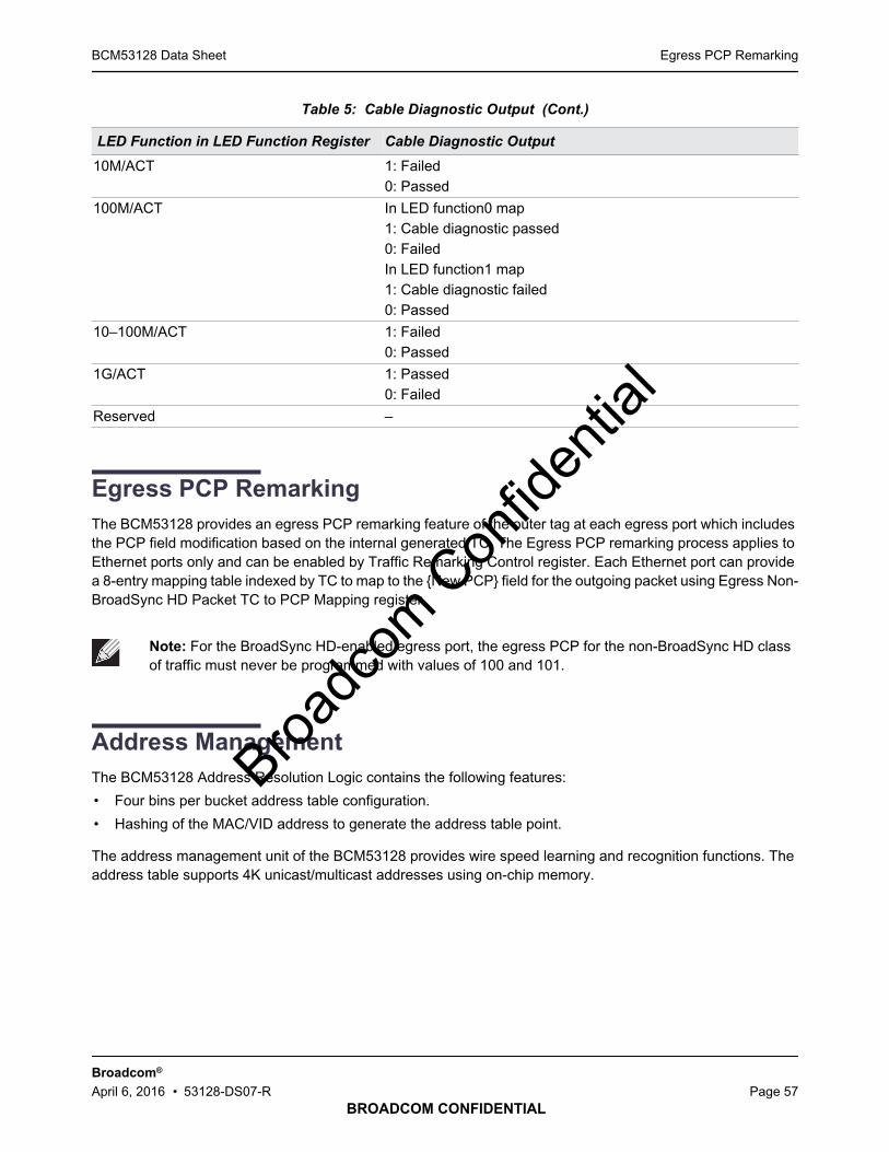
Egress PCP RemarkingBCM53128 Data Sheet
BROADCOM CONFIDENTIAL
Broadcom®
April 6, 2016 • 53128-DS07-R Page 57
Egress PCP Remarking
The BCM53128 provides an egress PCP remarking feature of the outer tag at each egress port which includesthe PCP field modification based on the internal generated TC. The Egress PCP remarking process applies toEthernet ports only and can be enabled by Traffic Remarking Control register. Each Ethernet port can providea 8-entry mapping table indexed by TC to map to the {New PCP} field for the outgoing packet using Egress Non-BroadSync HD Packet TC to PCP Mapping register.
Address Management
The BCM53128 Address Resolution Logic contains the following features:
• Four bins per bucket address table configuration.
• Hashing of the MAC/VID address to generate the address table point.
The address management unit of the BCM53128 provides wire speed learning and recognition functions. Theaddress table supports 4K unicast/multicast addresses using on-chip memory.
10M/ACT 1: Failed0: Passed
100M/ACT In LED function0 map1: Cable diagnostic passed0: FailedIn LED function1 map1: Cable diagnostic failed0: Passed
10–100M/ACT 1: Failed0: Passed
1G/ACT 1: Passed0: Failed
Reserved –
Note: For the BroadSync HD-enabled egress port, the egress PCP for the non-BroadSync HD classof traffic must never be programmed with values of 100 and 101.
Table 5: Cable Diagnostic Output (Cont.)
LED Function in LED Function Register Cable Diagnostic Output
Broadc
om C
onfid
entia
l

Address ManagementBCM53128 Data Sheet
BROADCOM CONFIDENTIAL
Broadcom®
April 6, 2016 • 53128-DS07-R Page 58
Address Table Organization
The MAC addresses are stored in embedded SRAM. Each bucket contains four entries or bins. The addresstable has 1K buckets with four entries in each bucket. This allows up to four different MAC addresses with thesame hashed index bits to be simultaneously mapped into the address table. In the ARL DA/SA lookup process,it hashes a 10-bit search index and read out bin0 and bin1 in the first cycle, and read out bin2 and bin3 in thesecond cycle. These four entries are used for ARL routing and learning.
Figure 9: Address Table Organization
The index to the address table is computed using a hash algorithm based on the MAC address and the VLANID (VID) if enabled.
The hash algorithm uses the CRC-CCITT polynomial. The input to the hash is reduced to a 16-bit CRC hashvalue. Bits[9:0] of the hash are used as an index to the approximately 4K locations of the address table.
The CRC-CCITT polynomial is:
x16+x12+x5+1
Note: In the Enable IEEE 802.1Q and VLAN Learning Mode both the MAC address and the VLAN ID(VID) are used to compute the hashed index. See “IEEE 802.1Q VLAN” on page 39 for more information.
MAC Address [47:0]HASH
FunctionVID [11:0]
Hash Index [9:0]
bin0 bin1bin3bin2
4K ARL Table000000
0003FF
V S A TC CON Rsvd PortID MACADDRVID[11:0]
V S A TC CON MCAST MAP MACADDRVID[11:0]
Unicast Address
Multicast Address
Four bins per index
Broadc
om C
onfid
entia
l
Address ManagementBCM53128 Data Sheet
BROADCOM CONFIDENTIAL
Broadcom®
April 6, 2016 • 53128-DS07-R Page 59
Address Learning
Information is gathered from received unicast packets and learned or stored for the future purpose of forwardingframes addressed to the receiving port. During the receive process, the frame information (such as the SourceAddress [SA] and VID) is saved until completion of the packet. An entry is created in the ARL table memory ifthe following conditions are met:
• The packet has been received without error.
• The packet is of legal length.
• The packet has a unicast SA.
• If using IEEE 802.1Q VLAN, the packet is from an SA that belongs to the indicated VLAN domain.
• The packet does not have a reserved multicast destination address. The Multicast Learning bit of theReserved Multicast Control register can disable this condition.
• There is free space available in memory to which the hashed index points.
When unicast packets are dynamically learned, the VALID bit is set, the AGE bit is set, and the STATIC bit iscleared in the entry. See Table 7 on page 60 for a description of a unicast ARL entry.
Multicast addresses are not learned into the ARL table, but must be written using one of the “ProgrammingInterfaces” on page 95. See “Writing an ARL Entry” on page 63 and Table 9 on page 61 for more information.
Address Resolution and Frame Forwarding
Received packets are forwarded based on the information learned or written into the ARL table. Addressresolution is the process of locating this information and assigning a forwarding destination to the packet. Thedestination address (DA) and VID of the received packet are used to calculate a hashed index to the ARL table.The hashed index key is used by the address resolution function to locate a matching ARL entry. The frame isassigned a destination based on the forward field (PORTID or FWD_PRT_MAP) of the ARL entry. If the addressresolution function fails to return a matching ARL entry, the packet is flooded to all appropriate ports. Thefollowing two sections describe the specifics of address resolution and frame forwarding for “Unicast Addresses”on page 59 and “Multicast Addresses” on page 61.
Unicast Addresses
Frames containing a unicast destination address are assigned a forwarding field corresponding to a single port.Listed below is the unicast address-resolution algorithm:
• If the multiport addressing feature is enabled and the DA matches one of the programmed multiportaddresses, then it is forwarded accordingly. See “Using the Multiport Addresses” on page 65.
• The lower 10 bits of the hashed index key are used as a pointer into the address table memory, and theentry is retrieved.
• If the valid indicator is set and the address stored at one of the locations matches the index key of thepacket received, the forwarding field port ID is assigned to the destination port of the packet.
– If the destination port matches the source port, the packet is not forwarded.
• If the address resolution function fails to return a matching valid ARL entry and the unicast DLF forward bitis set, the frame is forwarded according to the port map in the Unicast Lookup Failed Forward Map register.
• Otherwise, the packet is flooded to all appropriate ports.
Broadc
om C
onfid
entia
l
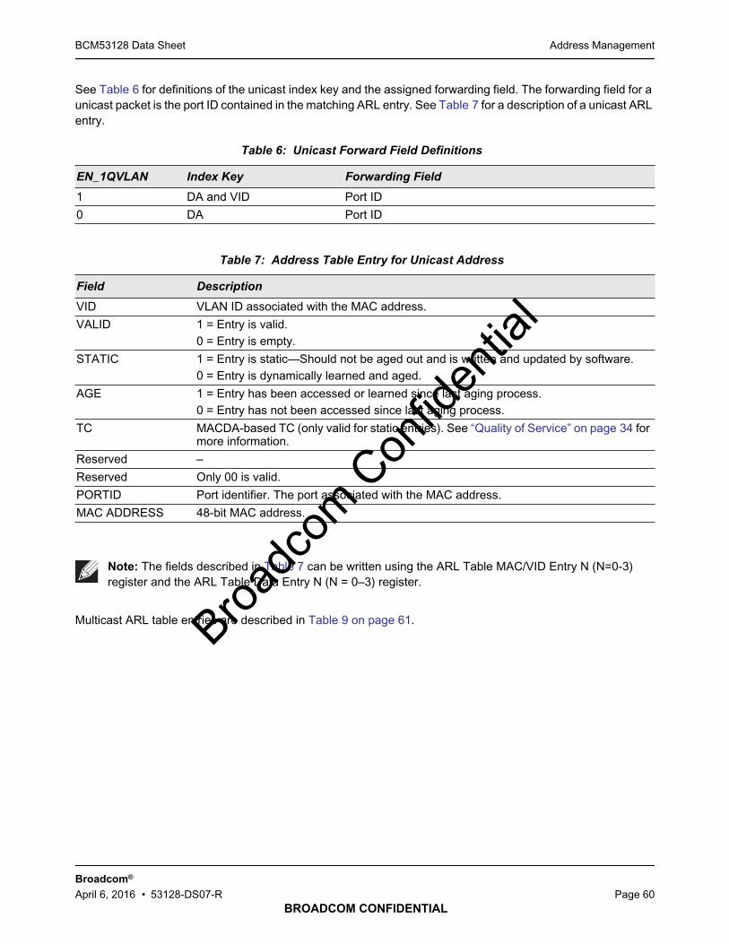
Address ManagementBCM53128 Data Sheet
BROADCOM CONFIDENTIAL
Broadcom®
April 6, 2016 • 53128-DS07-R Page 60
See Table 6 for definitions of the unicast index key and the assigned forwarding field. The forwarding field for aunicast packet is the port ID contained in the matching ARL entry. See Table 7 for a description of a unicast ARLentry.
Multicast ARL table entries are described in Table 9 on page 61.
Table 6: Unicast Forward Field Definitions
EN_1QVLAN Index Key Forwarding Field
1 DA and VID Port ID
0 DA Port ID
Table 7: Address Table Entry for Unicast Address
Field Description
VID VLAN ID associated with the MAC address.
VALID 1 = Entry is valid.0 = Entry is empty.
STATIC 1 = Entry is static—Should not be aged out and is written and updated by software.0 = Entry is dynamically learned and aged.
AGE 1 = Entry has been accessed or learned since last aging process.0 = Entry has not been accessed since last aging process.
TC MACDA-based TC (only valid for static entries). See “Quality of Service” on page 34 formore information.
Reserved –
Reserved Only 00 is valid.
PORTID Port identifier. The port associated with the MAC address.
MAC ADDRESS 48-bit MAC address.
Note: The fields described in Table 7 can be written using the ARL Table MAC/VID Entry N (N=0-3)register and the ARL Table Data Entry N (N = 0–3) register.
Broadc
om C
onfid
entia
l

Address ManagementBCM53128 Data Sheet
BROADCOM CONFIDENTIAL
Broadcom®
April 6, 2016 • 53128-DS07-R Page 61
Multicast Addresses
Frames containing a multicast destination address are assigned a forwarding field corresponding to multipleports specified in a port map. Multicast frames are assigned a forwarding field corresponding to a multicast portmap from the matching ARL entry (see “Address Management” on page 57). If no matching ARL entry is found,the packet is flooded to all appropriate ports. Listed below is the multicast address resolution algorithm:
• If the DA matches one of the globally assigned reserved addresses between 01-80-C2-00-00-00 and 01-80-C2-00-00-2F, the packet is handled as described in Table 10 on page 62.
• If the multiport addressing feature is enabled and the DA matches one of the programmed MultiportAddresses, then it is forwarded accordingly. See “Using the Multiport Addresses” on page 65.
• Otherwise, the lower 10 bits of the hashed index key are used as a pointer into the ARL table memory, andthe entry is retrieved.
• If the valid indicator is set, and the address stored at the entry locations matches the index key of thepacket received, the forwarding field port map is assigned to the destination port of the packet.
• If the address resolution function fails to return a matching valid ARL entry and the multicast DLF forwardbit is set (see “Address Management” on page 57), the frame is forwarded according to the port map in theMulticast Lookup Failed Forward Map register.
• Otherwise, all other multicast and broadcast packets are flooded to all appropriate ports.
See Table 8 for definitions of the multicast index key and the assigned forwarding field. The forwarding field fora multicast packet is the port map contained in the matching ARL entry. See Table 9 for a description of amulticast ARL entry. See “Accessing the ARL Table Entries” on page 63 for more information.
Table 8: Multicast Forward Field Definitions
EN_1QVLAN Unicast/Multicast Index Key Forwarding Field
1 Unicast DA and VID Port ID
0 Unicast DA Port ID
1 Multicast DA and VID FWD_PRT_MAP
0 Multicast DA FWD_PRT_MAP
Table 9: Address Table Entry for Multicast Address
Field Description
VID VLAN ID associated with the MAC address.
VALID 1 = Entry is valid.0 = Entry is empty.
STATIC 1 = Entry is static—This entry is not aged out and is written and updated by software.0 = Not defined.
AGE The AGE bit is ignored for static ARL table entries.
TC MACDA-based TC (only valid for static entries). See “Quality of Service” on page 34 for moreinformation.
Reserved –
Broadc
om C
onfid
entia
l
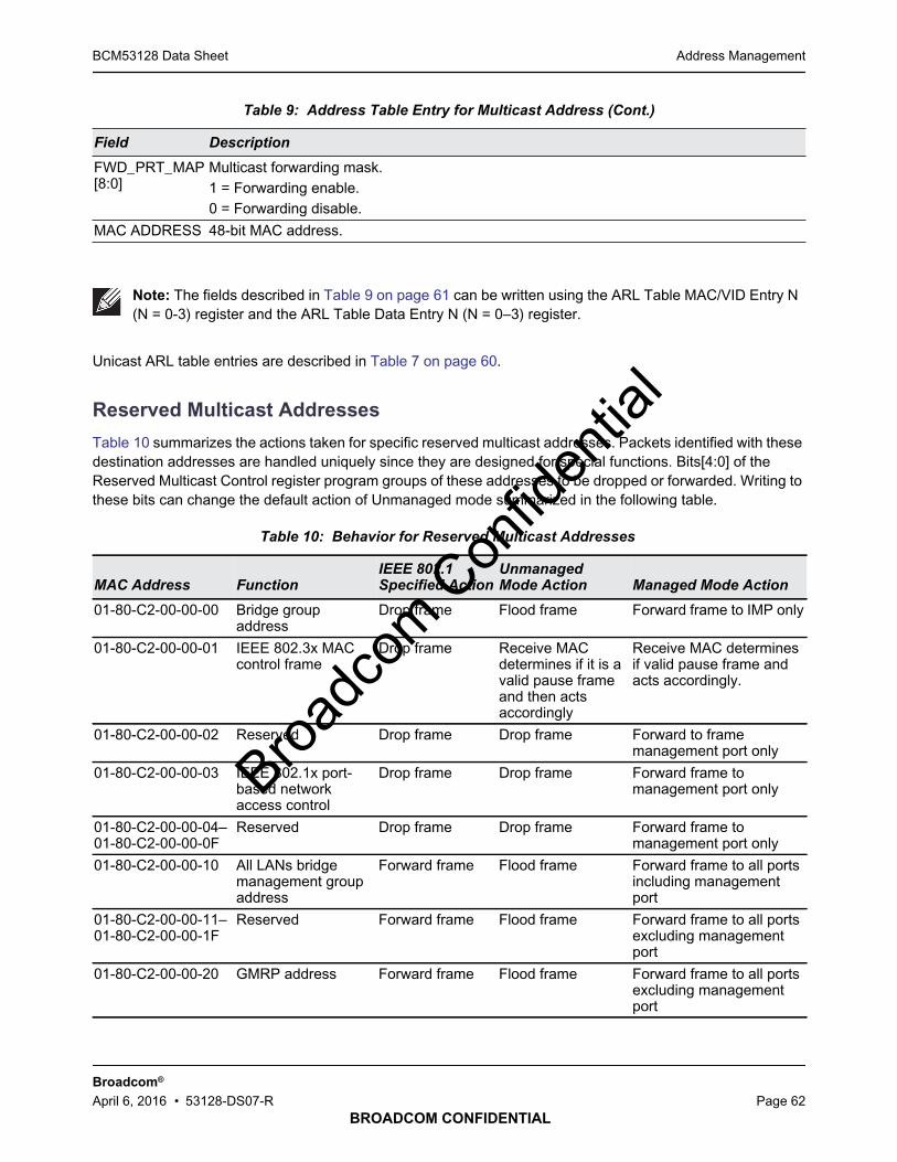
Address ManagementBCM53128 Data Sheet
BROADCOM CONFIDENTIAL
Broadcom®
April 6, 2016 • 53128-DS07-R Page 62
Unicast ARL table entries are described in Table 7 on page 60.
Reserved Multicast Addresses
Table 10 summarizes the actions taken for specific reserved multicast addresses. Packets identified with thesedestination addresses are handled uniquely since they are designed for special functions. Bits[4:0] of theReserved Multicast Control register program groups of these addresses to be dropped or forwarded. Writing tothese bits can change the default action of Unmanaged mode summarized in the following table.
FWD_PRT_MAP[8:0]
Multicast forwarding mask.1 = Forwarding enable.0 = Forwarding disable.
MAC ADDRESS 48-bit MAC address.
Note: The fields described in Table 9 on page 61 can be written using the ARL Table MAC/VID Entry N(N = 0-3) register and the ARL Table Data Entry N (N = 0–3) register.
Table 10: Behavior for Reserved Multicast Addresses
MAC Address FunctionIEEE 802.1Specified Action
UnmanagedMode Action Managed Mode Action
01-80-C2-00-00-00 Bridge groupaddress
Drop frame Flood frame Forward frame to IMP only
01-80-C2-00-00-01 IEEE 802.3x MACcontrol frame
Drop frame Receive MACdetermines if it is avalid pause frameand then actsaccordingly
Receive MAC determinesif valid pause frame andacts accordingly.
01-80-C2-00-00-02 Reserved Drop frame Drop frame Forward to framemanagement port only
01-80-C2-00-00-03 IEEE 802.1x port-based networkaccess control
Drop frame Drop frame Forward frame tomanagement port only
01-80-C2-00-00-04–01-80-C2-00-00-0F
Reserved Drop frame Drop frame Forward frame tomanagement port only
01-80-C2-00-00-10 All LANs bridgemanagement groupaddress
Forward frame Flood frame Forward frame to all portsincluding managementport
01-80-C2-00-00-11–01-80-C2-00-00-1F
Reserved Forward frame Flood frame Forward frame to all portsexcluding managementport
01-80-C2-00-00-20 GMRP address Forward frame Flood frame Forward frame to all portsexcluding managementport
Table 9: Address Table Entry for Multicast Address (Cont.)
Field Description
Broadc
om C
onfid
entia
l
Address ManagementBCM53128 Data Sheet
BROADCOM CONFIDENTIAL
Broadcom®
April 6, 2016 • 53128-DS07-R Page 63
Static Address Entries
The BCM53128 supports static ARL table entries that are created and updated using one of the “ProgrammingInterfaces” on page 95. These entries can contain either unicast or multicast destinations. The entries arecreated by writing the entry location using the Page 05h: ARL/VTBL Access registers and setting the STATICbit. The AGE bit is ignored. Static entries do not automatically learn MAC addresses or port associations andare not aged out by the automatic internal aging process. See “Writing an ARL Entry” on page 63 for details.
Accessing the ARL Table Entries
ARL table entries are accessed by one of two mechanisms. The first mechanism uses the ARL read/writecontrol, which allows an address-entry location to be read, modified, or written based on the value of a knownMAC address. The second mechanism searches the ARL table sequentially, returning all valid entries.
Reading an ARL Entry
To read an ARL entry:
1. Set the MAC address in the MAC Address Index register.
2. Set the VLAN ID in the VLAN ID Index register. This is necessary only if the VID is used in the index key.
3. Set the ARL_R/W bit to 1 in the ARL Table Read/Write Control register.
4. Set the START/DONE bit to 1 in the ARL Table Read/Write Control register. This initiates the read operation.
The MAC address and VID are used to calculate the hashed index to the ARL table. The matching ARL entry isread. The contents of entry are stored in the ARL Table MAC/VID Entry N (N = 0-3) register and the ARL TableData Entry N (N = 0–3) register.
Entries that do not have the VALID bit set should be ignored. The contents of the MAC/VID registers must becompared against the known MAC address and VID. Entries that do not match may be a valid entry, but are nota valid match for the index key. All other read entries are considered valid ARL entries.
Writing an ARL Entry
To write an ARL entry:
01-80-C2-00-00-21 GVRP address Forward frame Flood frame Forward frame to all portsexcluding managementport
01-80-C2-00-00-22–01-80-C2-00-00-2F
Reserved Forward frame Flood framea Forward frame to all portsexcluding managementport
a. Frames flood to all ports. Certain exclusions apply, such as VLAN restrictions.
Table 10: Behavior for Reserved Multicast Addresses (Cont.)
MAC Address FunctionIEEE 802.1Specified Action
UnmanagedMode Action Managed Mode Action
Broadc
om C
onfid
entia
l
Address ManagementBCM53128 Data Sheet
BROADCOM CONFIDENTIAL
Broadcom®
April 6, 2016 • 53128-DS07-R Page 64
1. Follow the steps in “Reading an ARL Entry” on page 63 to read the ARL entry matching the MAC addressand VID that are written to the table.
2. Keep the values that remain from the previous read operation.
• MAC Address Index register
• VLAN ID Index register
• ARL Table MAC/VID Entry N (N = 0-3) register
• ARL Table Data Entry N (N = 0–3) register
3. Modify the correct entry as necessary. Set the STATIC bit so that the entry is not aged out.
4. Set the ARL_R/W bit to 0 in the ARL Table Read/Write Control register.
5. Set the START/DONE bit to 1 in the ARL Table Read/Write Control register. This initiates the write operation.
The MAC address and VID are used to calculate the hashed index to the ARL table.
Searching the ARL Table
The second method to access the ARL table is through the ARL search control. The entire ARL table is searchedsequentially, revealing each valid ARL entry. Setting the Start/Done bit in the ARL Table Search Control registerbegins the search from the top of the ARL table. This bit is cleared when the search is complete. During the ARLsearch, the Search Valid bit indicates when a found valid entry is available in the ARL Table Search MAC/VIDResult N (N = 0–1) register and the ARL Table Search Data Result N (N = 0–1) register. When the host readsthe contents of the ARL Table Search Data Result 1 register which located in Page 05h: Address 78h, the searchprocess automatically continues to seek the next valid entry in the address table. Invalid address entries areskipped, providing the host with an efficient way of searching the entire address table.
The ARL search and ARL read/write operations execute in parallel with other register accesses. This allows thehost processor to start a read, write, or search process and then read/write other registers, returning periodicallyto see if the operation has completed.
Address Aging
The aging process periodically removes dynamically learned addresses from the ARL table. When an ARL entryis learned or referenced, the AGE bit is set to 1. The aging process scans the ARL table at regular intervals,aging out entries not accessed during the previous one to two aging intervals. The aging interval isprogrammable using the Aging Enable and AGE TIME bit in the Aging Time Control register.
Entries that are written and updated using one of the “Programming Interfaces” on page 95, should have theSTATIC bit set. Thus, they are not affected by the aging process.
For each entry in the ARL table, the aging process performs the following:
• If the VALID bit is not set, no further action is required.
• If the VALID bit is set and the STATIC is set, no further action is required.
• If the VALID bit is set, the STATIC bit is not set, and the AGE bit is set, then clear the AGE bit. This keepsthe entry in the table, but marks it so that it is removed if it is not accessed before the subsequent agingscan.
Broadc
om C
onfid
entia
l

Power Savings ModesBCM53128 Data Sheet
BROADCOM CONFIDENTIAL
Broadcom®
April 6, 2016 • 53128-DS07-R Page 65
• If the VALID bit is set, the STATIC bit is not set, and the AGE bit is reset, then reset the VALID bit. Thiseffectively deletes the entry from the ARL table. The entry has been aged out.
Fast Aging
The fast aging function can be enabled per port or VLAN ID:
The port fast aging can be enabled by setting the Start/Done of the Fast-Aging Control register, the Fast Age AllPorts bit of the Fast-Aging Port Control register, and the appropriate port bits in the Fast-Aging Port Controlregister.
The VLAN ID fast aging can be enabled by setting the Start/Done of the Fast-Aging Control register, the FastAge All VID bit of the Fast-Aging VID Control register, and the appropriate VLAN ID bits of the Fast-Aging VIDControl register.
Using the Multiport Addresses
The Multiport Address N (N = 0–5) register can be used to forward a given MAC address and Ether Type tomultiple ports. Packets with a corresponding DA are forwarded to the port map contained in the Multiport VectorN (N = 0–5) register. These registers must be controlled using Multiport Control register.
Power Savings Modes
The BCM53128 offers different power savings modes for different operating states. All the power saving schemeare implemented without any external CPU requirement. The various power savings modes are:
• Auto Power Down Mode: This is a stand alone PHY feature which is enabled by a register bit setting. ThePHY shuts off the analog portion of the circuitry when cable is not connected or the link partner power isdown.
• Energy Efficient Ethernet (EEE) Mode: Energy Efficient Ethernet is IEEE802.1az, an extension of theIEEE802.3 standard. IEEE defines support for the PHY to operate in Low Power Idle (LPI) mode. Whenenabled, this mode supports QUIET times during low link utilization, allowing the both sides of link todisable portions of each PHY's operating circuitry and save power.
• Short Cable Mode (Green Mode): This mode requires the CPU to run the cable diagnostics, and the CPUenables power savings mode based on the cable length measurement result.
• Deep Green Mode: This mode also requires the CPU to recognize the long period power down time andshut off the PHY power and the PLL to the PHY core. The BCM53128 enters normal operation andestablishes a link when a signal is detected at the PHY input.
Note: The Multiport Address N (N = 0–5) register is the only mechanism for TS Protocol qualification forthe BroadSync HD application. It can be enabled by Multiport Control register.
Broadc
om C
onfid
entia
l

Power Savings ModesBCM53128 Data Sheet
BROADCOM CONFIDENTIAL
Broadcom®
April 6, 2016 • 53128-DS07-R Page 66
Auto Power Down Mode
Auto Power Down mode saves PHY power consumption while the link is down. When the user enables the AutoPower Down mode through a PHY register bit setting, the PHY goes into the power savings mode automaticallywhenever it is in linkdown state. During the Power Down state, the PHY wakes up every 2.7 or 5.4 seconds,depending on the register settings, and checks for a link signal. If no link signal is detected, then the PHY goesback to Power Down state, or the PHY wakes up and resumes the link process.
Automatic Power Down mode applies to the following conditions:
1. Cable is plugged in, but the link partner is shut down (for example, when a PC is off), so the port is in linkdown state.
2. Cable is unplugged, so the port is in link down state.
Energy Efficient Ethernet Mode
Energy Efficient Ethernet power savings mode saves PHY consumption while the link is up but when extendedidle periods may exist between packet traffic. In EEE power savings mode PHY power consumption is scalableto the actual bandwidth utilization. The PHY can go in to “Quiet” mode (low-power idle mode) when there is nodata to be transmitted. This feature is based on the latest IEEE 802.3az standard. The EEE supporting capabilityof the link partner is a must for this feature to work, and the discovery of the capability is during auto-negotiationthrough Link Layer Discovery Protocol (LLDP). This EEE feature is an embedded PHY feature and no externalCPU is required.
In this mode, the MAC determines when to enter low power mode by examining the state of the transmit queuesassociated with each MAC. Four simple adjustments (settings) are used to trigger (optimize) the behavior ofEEE control policy. These adjustments are:
• Global Buffer occupancy threshold
• Two-part sleep delay timer
• Minimum low-power idle duration timer
• Wake transition timer
The two-way communication between the PHY and its link partner is required for the PHY to achieve the powersavings on both sides. The transmit PHY sends a sleep symbol to the link partner, and the link partner enterslow power state. When the transmit PHY sends a wake symbol, the regular packet transfer mode resumes. Fordetails on how the mode works and how to set up the conditions, please refer to the Layout and Design Guide(document number 53128-AN1xx-R).
Short Cable Mode (Green Mode)
The Short Cable Power Savings mode (called Green mode) requires a CPU. In the BCM53128, a dedicatedembedded 8051 processor is used to implement this feature. Software running in the 8051 triggers the cablediagnostic routine on a schedule programmed by the user (for example, upon every power up or every new link-up). The diagnostic routine obtains the length of the cable connected to the port. Then, the CPU reduces thePHY receiver power based on the measured cable length. It is for the Giga link only and the maximum supportedcable length is 30m.
Broadc
om C
onfid
entia
l

Power Savings ModesBCM53128 Data Sheet
BROADCOM CONFIDENTIAL
Broadcom®
April 6, 2016 • 53128-DS07-R Page 67
Deep Green Mode
The Deep Green Power Savings mode is a step deeper than the Auto Power Down Power Savings mode. TheDeep Green Power Savings mode can be enabled through the internal 8051 microcontroller by setting theEn_Green strap pin high. The Auto Power Down Power Savings mode is per port, but the Deep Green PowerSavings mode is per PHY core base with a common PLL. When the ports that are sharing a PLL are linkeddown, the Auto Power Down mode is enabled (Register Page 10h – 17h, Address 38h, Shadow 01010b), andthe DLL Auto Power-Down mode is enabled (Register Page 10h – 17h, Address 38h, Shadow 00101b), thenthe PHYs enter the Deep Green Power Savings mode. In this mode, all the PHY circuits are powered downexcept the energy detection circuit, and the energy detection circuit constantly monitors the energy on the line.Upon signal energy detection, the BCM53128 enters normal operation and establishes a link if energy isdetected. The Deep Green Power Savings mode is most effective when the user expects no activities on theline for a long period of time.
Broadc
om C
onfid
entia
l
System Functional BlocksBCM53128 Data Sheet
BROADCOM CONFIDENTIAL
Broadcom®
April 6, 2016 • 53128-DS07-R Page 68
Section 3: System Functional Blocks
Overview of System Functional Blocks
The BCM53128 include the following blocks:
• “Media Access Controller”
• “Integrated 10/100/1000 PHY” on page 70
• “Frame Management” on page 79
• “MIB Engine” on page 83
• “Integrated High-Performance Memory” on page 90
• “Switch Controller” on page 90
Each of these is discussed in more detail in the following sections.
Media Access Controller
The BCM53128 contains six 10/100/1000 GMACs, and one MAC.
The MAC automatically selects the appropriate speed (CSMA/CD or full-duplex) based on the PHY auto-negotiation result. In full-duplex mode, IEEE 802.3x PAUSE frame-based flow control is also determinedthrough auto-negotiation. The MAC is IEEE 802.3-, IEEE 802.3u-, and IEEE 802.3x-compliant.
Receive Function
The MAC initiates frame reception following the assertion of receive data valid indication from the physical layer.The MAC monitors the frame for the following error conditions:
• Receive error indication from the PHY
• Runt frame error if frame is fewer than 64 bytes
• CRC error
• Long frame error if frame is greater than the standard maximum frame size or 9,720 bytes for jumbo-enabled ports.
If no errors are detected, the frame is processed by the switch controller. Frames with errors are discarded.Receive functions can be disabled by writing to Port Traffic Control register.
Note: Frames longer than standard max frame size which configured using Standard Max Frame Sizeregister are considered oversized frames. When jumbo-frame mode is enabled, only the frames longerthan 9,720 bytes are bad frames and dropped.
Broadc
om C
onfid
entia
l
Media Access ControllerBCM53128 Data Sheet
BROADCOM CONFIDENTIAL
Broadcom®
April 6, 2016 • 53128-DS07-R Page 69
Transmit Function
Frame transmission begins with the switch controller queuing a frame to the MAC transmitter. The frame datais transmitted as received from the switch controller. The transmit controller is responsible for preambleinsertion, carrier deferral, collision backoff, and inter-packet gap enforcement.
In 10/100 Mbps half-duplex mode, when a frame is queued for transmission, the transmit controller behaves asspecified by the IEEE 802.3 requirements for frame deferral. Following deferral, the transmitter adds 8 bytes ofpreamble and SFD to the frame data received from the switch controller. If, during frame transmission, a collisionis observed and the collision window timer has not expired, the transmit controller asserts jam and then executesthe backoff algorithm. The frame is retransmitted when appropriate. On the 16th consecutive collision, thebackoff algorithm starts over at the initial state, the collision counter is reset and attempts to transmit the currentframe continue. Following a late collision, the frame is aborted, and the switch controller is allowed to queue thenext frame for transmission.
While in full-duplex mode, the transmit controller ignores carrier activity and collision indication. Transmissionbegins after the switch controller queues the frame, and the 96-bit times of IPG have been observed. Transmitfunctions can be disabled by writing to Port Traffic Control register.
Flow Control
The BCM53128 implement an intelligent flow-control algorithm to minimize the system impact resulting fromtraffic congestion. Buffer memory allocation is adaptive to the status of each port’s speed and duplex mode,providing an optimal balance between flow management and per-port memory depth. The BCM53128 initiateflow control in response to buffer memory conditions on a per-port basis.
The MACs are capable of flow control in both full-and half-duplex modes.
10/100 Mbps Half-Duplex
In 10/100 half-duplex mode, the MAC back-pressures a receiving port by transmitting a 96-bit time jam packetto the port. A single jam packet is asserted for each received packet for the duration of the time the port is in theflow-control state.
10/100/1000 Mbps Full-Duplex
Flow control in full-duplex mode functions as specified by the IEEE 802.3x requirements. In the receiver, MACflow-control frames are recognized and, when properly received, set the flow-control pause time for the transmitcontroller. The pause time is assigned from the 2-byte pause time field following the pause opcode. MAC controlPAUSE frames are not forwarded from the receiver to the switch controller.
When the switch controller requests flow control, the transmit controller transmits a MAC control PAUSE framewith the pause time set to maximum. When the condition that caused the flow control state is no longer present,a second MAC control PAUSE frame is sent with the pause time field set to 0.
The flow control capabilities of the BCM53128 are enabled based on the results of auto-negotiation and the stateof the ENFDXFLOW and ENHDXFLOW control signals loaded during reset. Flow control in half-duplex modeis independent of the state of the link partner flow control (IEEE 802.3x) capability. See Table 11 for detailedinformation.
Broadc
om C
onfid
entia
l

Integrated 10/100/1000 PHYBCM53128 Data Sheet
BROADCOM CONFIDENTIAL
Broadcom®
April 6, 2016 • 53128-DS07-R Page 70
Integrated 10/100/1000 PHY
There are eight integrated PHY blocks in the BCM53128. For more information see “Copper Interface” onpage 92. The following sections describe the operations of the internal PHY block.
Encoder
There are eight integrated PHY blocks in the BCM53128. The PHY is the Ethernet transceiver that appropriatelyprocesses data presented by the MAC into an analog data stream to be transmitted at the MDI interface, whichperforms the reverse process on data received at the MDI interface. The registers of the PHY are read usingthe “Programming Interfaces” on page 95. The following sections describe the operations of the internal PHYblock. For more information, see “Copper Interface” on page 92.
In 10BASE-T mode, Manchester encoding is performed on the data stream that is transmitted on the twisted-pair cable. The multimode transmit digital-to-analog converter (DAC) performs preequalization for 100m ofCategory 3 cabling.
In 100BASE-TX mode, the BCM53128 transmits a continuous data stream over the twisted-pair cable. Thetransmit packet is encapsulated by replacing the first two nibbles of preamble with a start-of-stream delimiter (/J/K codes) and appending an end-of-stream delimiter (/T/R codes) to the end of the packet. The transmitterrepeatedly sends the idle code group between packets. The encoded data stream is serialized and thenscrambled by the stream cipher block, as described in “Stream Cipher” on page 73. The scrambled data is thenencoded into MLT3 signal levels.
Table 11: Flow Control Modes
Link Partner FlowControl (IEEE802.3x)
Control InputENFDXFLOW
Control InputENHDXFLOW
Auto-negotiatedLink Speed Flow Control Mode
X X 0 Half-duplex Disabled
X X 1 Half-duplex Jam pattern
0 0 X Full-duplex Disabled
0 1 X Full-duplex Disabled
1 0 X Full-duplex Disabled
1 1 X Full-duplex IEEE 802.3x flow control
Broadc
om C
onfid
entia
l

Integrated 10/100/1000 PHYBCM53128 Data Sheet
BROADCOM CONFIDENTIAL
Broadcom®
April 6, 2016 • 53128-DS07-R Page 71
In 1000BASE-T mode, the BCM53128 simultaneously transmits and receives a continuous data stream on all4 pairs of the Category 5 cable. Byte-wide data from the transmit data pins is scrambled when the transmitenable is asserted, and the trellis (a PAM5 symbol on each of the four twisted-pairs) is encoded into a four-dimensional code group and then inserted into the transmit data stream. The transmit packet is encapsulatedby replacing the first 2 bytes of the preamble with a start-of-stream delimiter, and appending an end-of-streamdelimiter to the end of the packet. When the transmit error input is asserted during a packet transmission, atransmit error code group is sent in place of the corresponding data code group. The transmitter sends idle codegroups or carrier extend code groups between packets. Carrier extension is used by the MAC to separatepackets within a multiple-packet burst and is indicated by asserting the transmit error signal and placing 0Fh onthe transmit data pins while the transmit enable is low. A carrier extend error is indicated by replacing thetransmit data input with 1Fh during carrier extension.
The encoding complies with IEEE standard IEEE 802.3ab and is fully compatible with previous versions of theBroadcom 1000BASE-T PHYs.
Decoder
In 10BASE-T mode, Manchester decoding is performed on the data stream.
In 100BASE-TX mode, following equalization and clock recovery, the receive data stream is converted fromMLT3 to serial nonreturn-to-zero (NRZ) data. The NRZ data is descrambled by the stream cipher block, asdescribed later in this document. The descrambled data is then deserialized and aligned into 5-bit code groups.The 5-bit code groups are decoded into 4-bit data nibbles. The start-of-stream delimiter is replaced withpreamble nibbles, and the end-of-stream delimiter and idle codes are replaced with 0h. The decoded data isdriven onto the MII receive data pins. When an invalid code group is detected in the data stream, the BCM53128asserts the MII receive error (RX_ER) signal. RX_ER is also asserted when the link fails, or when thedescrambler loses lock during packet reception.
In 1000BASE-T mode, the receive data stream is:
• Passed through the Viterbi decoder
• Descrambled
• Translated back into byte-wide data
The start-of-stream delimiter is replaced with preamble bytes, and the end-of-stream delimiter and idle codesare replaced with 00h. Carrier extend codes are replaced with 0Fh or 1Fh. Decoding complies with IEEEstandard IEEE 802.3ab and is fully compatible with previous versions of Broadcom 1000BASE-T PHYs.
Link Monitor
In 10BASE-T mode, a link-pulse detection circuit constantly monitors the TRD pins for the presence of valid linkpulses.
In 100BASE-TX mode, receive signal energy is detected by monitoring the receive pair for transitions in thesignal level. Signal levels are qualified using squelch detect circuits. When no signal is detected on the receivepair, the link monitor enters the Link Fail state and the transmission and reception of data packets is disabled.When a valid signal is detected on the receive pair for a minimum of 1 ms, the link monitor enters the Link Passstate, and the transmit and receive functions are enabled.
Broadc
om C
onfid
entia
l

Integrated 10/100/1000 PHYBCM53128 Data Sheet
BROADCOM CONFIDENTIAL
Broadcom®
April 6, 2016 • 53128-DS07-R Page 72
Following auto-negotiation in 1000BASE-T mode, the master transceiver begins sending data on the media.The slave transceiver also begins transmitting when it has recovered the master transceiver’s timing. Each endof the link continuously monitors its local receiver status. When the local receiver status has been good for atleast 1 microsecond, the link monitor enters the Link Pass state, and the transmission and reception of datapackets are enabled. When the local receiver status is bad for more than 750 ms, the link monitor enters theLink Fail state and the transmission and reception of data packets are disabled.
Digital Adaptive Equalizer
The digital adaptive equalizer removes intersymbol interference (ISI) created by the transmission channelmedia. The equalizer accepts sampled unequalized data from the analog-to-digital converter (ADC) on eachchannel and produces equalized data. The BCM53128 achieves an optimum signal-to-noise ratio by using acombination of feed forward equalization (FFE) and decision feedback equalization (DFE) techniques. Underharsh noise environments, these powerful techniques achieve a bit error rate (BER) of less than 1 x 10–12 fortransmissions up to 100m on Category 5 twisted-pair cabling (100m on Category 3 UTP cable for 10BASE-Tmode). The all-digital nature of the design makes the performance very tolerant to noise. The filter coefficientsare self-adapting to accommodate varying conditions of cable quality and cable length.
Echo Canceler
Because of the bidirectional nature of the channel in 1000BASE-T mode, an echo impairment is caused by eachtransmitter. The output of the echo filter is added to the FFE output to remove the transmitted signal impairmentfrom the incoming receive signal. The echo canceler coefficients are self-adapting to manage the varying echoimpulse responses caused by different channels, transmitters, and environmental conditions.
Cross Talk Canceler
The BCM53128 transmits and receives a continuous data stream on four channels. For a given channel, thesignals sent by the other three local transmitters cause impairments on the received signal because of near-endcrosstalk (NEXT) between the pairs. It is possible to cancel the effect because each receiver has access to thedata for the other three pairs that cause this interference. The output of the adaptive NEXT canceling filters isadded to the FFE output to cancel the NEXT impairment.
Analog-to-Digital Converter
Each receive channel has its own 125-MHz analog-to-digital converter (ADC) that samples the incoming dataon the receive channel and feeds the output to the digital adaptive equalizer. Advanced analog circuit techniquesachieve the following results:
• Low offset
• High power-supply noise rejection
• Fast settling time
• Low bit error rate
Broadc
om C
onfid
entia
l
Integrated 10/100/1000 PHYBCM53128 Data Sheet
BROADCOM CONFIDENTIAL
Broadcom®
April 6, 2016 • 53128-DS07-R Page 73
Clock Recovery/Generator
The clock recovery and generator block creates the transmit and receive clocks for 1000BASE-T, 100BASE-TX,and 10BASE-T operation.
In 10BASE-T or 100BASE-TX mode, the transmit clock is locked to the 25-MHz crystal input, and the receiveclock is locked to the incoming data stream.
In 1000BASE-T mode, the two ends of the link perform loop timing. One end of the link is configured as themaster, and the other is configured as the slave. The master transmit and receive clocks are locked to the 25-MHz crystal input. The slave transmit and receive clocks are locked to the incoming receive data stream. Looptiming allows for the cancellation of echo and NEXT impairments by ensuring that the transmitter and receiverat each end of the link are operating at the same frequency.
Baseline Wander Correction
1000BASE-T and 100BASE-TX data streams are not always DC-balanced. Because the receive signal mustpass through a transformer, the DC offset of the differential receive input can vary with data content. This effect,which is known as baseline wander, can greatly reduce the noise immunity of the receiver. The BCM53128automatically compensates for baseline wander by removing the DC offset from the input signal, therebysignificantly reducing the probability of a receive symbol error.
In 10BASE-T mode, baseline wander correction is not performed because the Manchester coding provides aperfect DC balance.
Multimode TX Digital-to-Analog Converter
The multimode transmit digital-to-analog converter (DAC) transmits PAM5, MLT3, and Manchester codedsymbols. The transmit DAC performs signal wave shaping that decreases the unwanted high frequency signalcomponents, reducing electromagnetic interference (EMI). The transmit DAC uses a voltage driven output withinternal terminations and hence, does not require external components or magnetic supply for operation thusreducing system complexity for routing and bill of materials.
Stream Cipher
In 1000BASE-T and 100BASE-TX modes, the transmit data stream is scrambled to reduce radiated emissionsand to ensure that there are adequate transitions within the data stream. The 1000BASE-T scrambler alsoensures that there is no correlation among symbols on the four different wire pairs and in the transmit andreceive data streams. The scrambler reduces peak emissions by randomly spreading the signal energy over thetransmit frequency range and eliminating peaks at certain frequencies. The randomization of the data streamalso assists the digital adaptive equalizers and echo/crosstalk cancelers. The algorithms in these circuits requirethere to be no sequential or cross-channel correlation among symbols in the various data streams.
In 100BASE-TX mode, the transmit data stream is scrambled by exclusive ORing the encoded serial datastream. This is done with the output of an 11-bit wide linear feedback shift register (LFSR), producing a 2047-bit nonrepeating sequence.
Broadc
om C
onfid
entia
l
Integrated 10/100/1000 PHYBCM53128 Data Sheet
BROADCOM CONFIDENTIAL
Broadcom®
April 6, 2016 • 53128-DS07-R Page 74
In 1000BASE-T mode, the transmit data stream is scrambled by exclusive ORing the input data byte with an 8-bit wide cipher text word. The cipher text word generates each symbol period from eight uncorrelated maximallength data sequences that are produced by linear remapping of the output of a 33-bit wide LFSR. After thescrambled data bytes are encoded, the sign of each transmitted symbol is again randomized by a 4-bit widecipher text word that is generated in the same manner as the 8-bit word. The master and slave transmitters usedifferent scrambler sequences to generate the cipher text words. For repeater or switch applications, where allports can transmit the same data simultaneously, signal energy is randomized further by using a unique seedto initialize the scrambler sequence for each PHY.
The receiver descrambles the incoming data stream by exclusive ORing it with the same sequence generatedat the transmitter. The descrambler detects the state of the transmit LFSR by looking for a sequencerepresenting consecutive idle code groups. The descrambler locks to the scrambler state after detecting asufficient number of consecutive idle codes. The BCM53128 enables transmission and reception of packet dataonly when the descrambler is locked. The receiver continually monitors the input data stream to ensure that ithas not lost synchronization by checking that inter-packet gaps containing idles or frame extensions arereceived at expected intervals. When the BCM53128 detects loss of synchronization, it notifies the remote PHYof the inability to receive packets (1000BASE-T mode only) and attempts to resynchronize to the received datastream. If the descrambler is unable to resynchronize for a period of 750 ms, the BCM53128 is forced into theLink Fail state.
In 10BASE-T mode, scrambling is not required to reduce radiated emissions.
Wire Map and Pair Skew Correction
During 1000BASE-T operation, the BCM53128 has the ability to automatically detect and correct some UTPcable wiring errors. The symbol decoder detects and compensates for (internal to the BCM53128) the followingerrors:
• Wiring errors caused by the swapping of pairs within the UTP cable.
• Polarity errors caused by the swapping of wires within a pair.
The BCM53128 also automatically compensates for differences in the arrival times of symbols on the four pairsof the UTP cable. The varying arrival times are caused by differing propagation delays (commonly referred toas delay skew) between the wire pairs. The BCM53128 can tolerate delay skews of up to 64 ns long. Auto-negotiation must be enabled to take advantage of the wire map correction.
During 10/100 Mbps operation, pair swaps are corrected. Delay skew is not an issue though, because only onepair of wires is used in each direction.
Automatic MDI Crossover
During copper auto-negotiation, one end of the link needs to perform an MDI crossover so that eachtransceiver’s transmitter is connected to the other receiver. The BCM53128 can perform an automatic media-dependent interface (MDI) crossover, eliminating the need for crossover cables or cross-wired (MDIX) ports.During auto-negotiation, the BCM53128 normally transmits and receives on the TRD pins.
When connecting to another device that does not perform MDI crossover, the BCM53128 automatically switchesits TRD in pairs when necessary to communicate with the remote device. When connecting to another devicethat does have MDI crossover capability, an algorithm determines which end performs the crossover function.
Broadc
om C
onfid
entia
l

Integrated 10/100/1000 PHYBCM53128 Data Sheet
BROADCOM CONFIDENTIAL
Broadcom®
April 6, 2016 • 53128-DS07-R Page 75
During 1000BASE-T operation, the BCM53128 swaps the transmit symbols on pairs 0 and 1 and pairs 2 and 3if auto-negotiation completes in the MDI crossover state. The 1000BASE-T receiver automatically detects pairswaps on the receive inputs and aligns the symbols properly within the decoder. The automatic MDI crossoverfunction cannot be disabled when in 1000BASE-T mode. During 10BASE-TX and 100BASE-T operation, pairswaps automatically occur within the device and do not require user intervention. The automatic MDI crossoverfunction by default only works when auto-negotiation is enabled. This function can be disabled during auto-negotiation by writing 1 to bit 14 of the PHY Extended Control register.
10/100BASE-TX Forced Mode Auto-MDIX
The automatic MDI crossover function can also be enabled when in forced 10BASE-T or forced 100BASE-TXmode. This feature allows the user to disable the copper auto-negotiation in either 10BASE-T or 100BASE-TXand still take advantage of the automatic MDI crossover function. Whenever the forced link is down for at least4 seconds, then auto-negotiation is internally enabled with its automatic MDI crossover function until link pulsesor 100Tx idles are detected. Once detected, the PHY returns to forced mode operation.
The user should set the same speed in register 0 and the auto-negotiation advertisement register 4.
Resetting the PHY
The BCM53128 provides a hardware reset pin, RESET, which resets all internal nodes to a known state.Hardware reset is accomplished by holding the RESET pin low for at least 1 ms. Once RESET is brought high,the PHY will complete its reset sequence within 5 ms. All outputs will be inactive until the PHY has completedits reset sequence. The PHY will keep the inputs inactive for 5 ms after the deassertion of hardware reset. Thehardware configuration pins and the PHY address pins will be read on the deassertion of hardware reset.
The BCM53128 also has a software reset capability. To enable the software reset, a 1 must be written to the bit.This bit is self-clearing, meaning that a second write operation is not necessary to end the reset. There is noeffect if 0 is written to this bit. Mode pins that are labelled sample on reset (SOR) are latched during hardwarereset. Similarly, software resets also latch new values for the SOR mode pins.
Note: This function only operates when the copper auto-negotiation is enabled.
Note: This function only operates when the copper auto-negotiation is disabled.
Broadc
om C
onfid
entia
l

Integrated 10/100/1000 PHYBCM53128 Data Sheet
BROADCOM CONFIDENTIAL
Broadcom®
April 6, 2016 • 53128-DS07-R Page 76
PHY Address
The BCM53128 has eight unique PHY addresses for MII management of the internal PHYs. The PHYaddresses for each port are as follows,
• PHY address for Port 0 is 0
• PHY address for Port 1 is 1
• PHY address for Port 2 is 2
• PHY address for Port 3 is 3
• PHY address for Port 4 is 4
• PHY address for Port 5 is 5
• PHY address for Port 6 is 6
• PHY address for Port 7 is 7
Super Isolate Mode
When in Super Isolate mode, the transmit and receive functions on the Copper Media Dependent Interface aredisabled (No link will be established with the PHY’s copper link partner). Any data received from the switch willbe ignored by the BCM53128 and no data will be sent from the BCM53128.
Standby Power-Down Mode
The BCM53128 can be placed into standby power-down mode using software commands. In this mode, all PHYfunctions except for the serial management interface are disabled. To enter standby power-down mode, set MIIControl register (Page 10h–17h: Address 00h), bit 11 = 1. There are three ways to exit standby power-downmode:
• Clear MII Control register (address 00h), bit 11 = 0.
• Set the software RESET bit 15, MII Control register (Page 10h–17h: Address 00h).
• Assert the hardware RESET pin.
Read or write operations to any MII register, other than MII Control register, while the device is in the standbypower-down mode returns unpredictable results. Upon exiting standby power-down mode, the BCM53128remains in an internal reset state for 40 µs and then resumes normal operation.Broa
dcom
Con
fiden
tial

Integrated 10/100/1000 PHYBCM53128 Data Sheet
BROADCOM CONFIDENTIAL
Broadcom®
April 6, 2016 • 53128-DS07-R Page 77
Auto Power-Down Mode
The BCM53128 can be placed into auto power-down mode. Auto power-down mode reduces device powerwhen the signal from the copper link partner is not present. The auto power-down mode works whether thedevice is in Auto-negotiation Enabled or Forced mode. This mode is enabled by setting bit 5 =1 of Auto Power-Down register. When auto power-down mode is enabled, the BCM53128 automatically enters the low-powermode when energy on the line is lost, and it resumes normal operation when energy is detected. When theBCM53128 is in auto power-down mode, it wakes up after 2.7s or 5.4s, which determined by bit 4 of Auto Power-Down register, and sends link pulses while monitoring for energy from the link partner. The BCM53128 entersnormal operation and establishes a link if energy is detected, otherwise the wake-up mode continues for aduration of 84 ms to 1260 ms. This is determined by the timer bits [3:0] of Auto Power-Down register. beforegoing back to low-power mode.
External Loopback Mode
The External Loopback mode allows in-circuit testing of the BCM53128 as well as the transmit path through themagnetics and the RJ-45 connector. External loopback can be performed with and without a jumper block.External loopback with a jumper block tests the path through the magnetics and RJ-45 connector. Externalloopback without the jumper block only tests the BCM53128’s transmit and receive circuitry. In 1000BASE-T,100BASE-TX, and 10BASE-T modes, a jumper block must be inserted into the RJ-45 connector to supportexternal loopback. The jumper block should have the following RJ-45 pins connected together:
1------------32------------64------------75------------8
Table 12 to Table 17 on page 78 describe how the external loopback is enabled for 1000BASE-T, 100BASE-TX,and 10BASE-T modes with and without a jumper block.
Table 12: 1000BASE-T External Loopback with External Loopback Plug
Register Writes Comments
Write 1800h to 1000BASE-T Control register Enable 1000BASE-T Master Mode
Write 0040h to MII Control register Enable Force 1000BASE-T
Write 8400h to Auxiliary Control register Enable External Loopback Mode with external loopbackplug
Table 13: 1000BASE-T External Loopback Without External Loopback Plug
Register Writes Comments
Write 1800h to 1000BASE-T Control register Enable 1000BASE-T Master Mode
Write 0040h to MII Control register Enable Force 1000BASE-T
Write 8400h to Auxiliary Control register Enable External Loopback Mode
Write 0014h to Auxiliary Control register Enable External Loopback Mode without external loopbackplug
Broadc
om C
onfid
entia
l
Integrated 10/100/1000 PHYBCM53128 Data Sheet
BROADCOM CONFIDENTIAL
Broadcom®
April 6, 2016 • 53128-DS07-R Page 78
Full-Duplex Mode
The BCM53128 supports full-duplex operation. While in full-duplex mode, a transceiver can simultaneouslytransmit and receive packets on the cable.
Copper Mode
When auto-negotiation is disabled, full-duplex operation can be enabled by setting bit 8 of MII Control register.
When auto-negotiation is enabled, the full-duplex capability is advertised for:
• 10BASE-T when bit 6 of Auto-Negotiation Advertisement register is set.
• 100BASE-T when bit 8 Auto-Negotiation Advertisement register is set.
• 1000BASE-T when bit 9 of 1000BASE-T Control register is set.
Table 14: 100BASE-TX External Loopback with External Loopback Plug
Register Writes Comments
Write 2100h to MII Control register Enable Force 100BASE-TX full-duplex mode
Table 15: 100BASE-TX External Loopback Without External Loopback Plug
Register Writes Comment
Write 2100h to MII Control register Enable Force 100BASE-TX full-duplex mode
Write 0014h to Auxiliary Control register Enable external loopback mode without external loopbackplug
Table 16: 10BASE-T External Loopback with External Loopback Plug
Register Writes Comments
Write 0100h to MII Control register Enable Force 10BASE-T full-duplex mode
Table 17: 10BASE-T External Loopback Without External Loopback Plug
Register Writes Comments
Write 0100h to MII Control register Enable Force 10BASE-T full-duplex mode
Write 0014h to Auxiliary Control register Enable external loopback mode without external loopbackplug
Note: To exit the External Loopback mode, a software or hardware reset is recommended.
Broadc
om C
onfid
entia
l

Frame ManagementBCM53128 Data Sheet
BROADCOM CONFIDENTIAL
Broadcom®
April 6, 2016 • 53128-DS07-R Page 79
Master/Slave Configuration
In 1000BASE-T mode, the BCM53128 and its link partner perform loop timing. One end of the link must beconfigured as the timing master, and the other end as the slave. Master/slave configuration is performed by theauto-negotiation function. The auto-negotiation function first looks at the manual master/slave configuration bitsadvertised by the local PHY and the link partner. If neither PHY requests manual configuration, then the auto-negotiation function looks at the advertised repeater/DTE settings. If one PHY is advertised as a repeater portand the other is advertised as a DTE port, then the repeater port is configured as the master and the DTE portas the slave. Each end generates an 11-bit random seed if the two settings are equal, and the end with thehigher seed is configured as the master. If the local PHY and the link partner generate the same random seed,then auto-negotiation is restarted.
If both ends of the link attempt to force the same manual configuration (both master or both slave), or the randomseeds match seven consecutive times, then the BCM53128 sets the Master/Slave Configuration Fault bit in the1000BASE-T Status register, and auto-negotiation is restarted. This is used to set the BCM53128 to manualmaster/slave configuration or to set the advertised repeater/DTE configuration.
Next Page Exchange
The 1000BASE-T configuration requires the exchange of three auto-negotiation next pages between theBCM53128 and its link partner. Exchange of 1000BASE-T Next Page information takes place automaticallywhen the BCM53128 is configured to advertise 1000BASE-T capability.
The BCM53128 also supports software controlled Next Page exchanges. This includes the three 1000BASE-TNext Pages, which are always sent first. The BCM53128 automatically generates the appropriate message codefield for the 1000BASE-T pages. When the BCM53128 is not configured to advertise 1000BASE-T capability,the 1000BASE-T Next Pages are not sent.
When the BCM53128 is not configured to advertise 1000BASE-T capability and bit 15 of the Auto-NegotiationAdvertisement register is set, the BCM53128 does not advertise Next Page ability.
Frame Management
The BCM53128 provides a Frame Management block that works in conjunction with one of the GMII portsoperate in IMP mode as the full duplex packet streaming interface to the external CPU, with in-band messagingmechanism for management purpose.
In-Band Management Port
The GMII port can be configured as the management port, using the Frame Management Port bits in the GlobalManagement Configuration register. When the GMII port is defined as the Frame Management Port, it is referredto as the in-band management port (IMP).
The IMP can be used as a full-duplex 10/100/1000-Mbps port, which can be used to forward managementinformation to the external management agent, such as BPDUs, mirrored frames, or frames addressed to otherstatic address entries that have been identified as a special interest to the management system.
Broadc
om C
onfid
entia
l

Frame ManagementBCM53128 Data Sheet
BROADCOM CONFIDENTIAL
Broadcom®
April 6, 2016 • 53128-DS07-R Page 80
As IMP is defined as the frame management port, normal frame data is forwarded to the port based on the stateof the RX_UCST_EN, RX_MCST_EN and RX_BCST_EN bits in the IMP Port Control register. If these bits arecleared, no frame data will be forwarded to the Frame Management Port, with the exception that frames meetingthe mirror ingress/egress rules criteria, will always be forwarded to the designated frame management port.
Packets transferred over the IMP port are tagged with the Broadcom proprietary header to carry the necessaryinformation which is of interest to the management entity running on the CPU, as shown below, except for thePAUSE frame. The IMP port must support normal Ethernet pause based flow control mechanism.
Figure 10: IMP Packet Encapsulation Format
The BRCM tag is designed for asymmetric operation across the IMP port. The information carried from theswitching device to the CPU is different from the information carried from the CPU to the switching device.
Similarly, the host system must insert the BRCM tag fields into frames it wished to send into the managementport, to be routed to specific egress ports. The OPCODE within the tag field determines how the frame ishandled, and allows frames to be forwarded using the normal address lookup using a port ID designation withinthe tag.
The BRCM tag are transmitted with the convention of highest significant octet first, followed by the next lowestsignificant octet, and so on, with the least significant bit of each octet transmitted out from the MAC first. So, forthe BRCM tag field in Table 18 on page 81 the most significant octet would be transmitted first (bits [24:31]), withbit 24 being the first bit transmitted.
Broadc
om C
onfid
entia
l
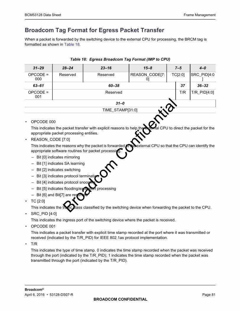
Frame ManagementBCM53128 Data Sheet
BROADCOM CONFIDENTIAL
Broadcom®
April 6, 2016 • 53128-DS07-R Page 81
Broadcom Tag Format for Egress Packet Transfer
When a packet is forwarded by the switching device to the external CPU for processing, the BRCM tag isformatted as shown in Table 18.
• OPCODE 000
This indicates the packet transfer with explicit reasons to help the external CPU to direct the packet for theappropriate packet processing entities.
• REASON_CODE [7:0]
This indicates the reasons why the packet is forwarded to the external CPU so that the CPU can identify theappropriate software routines for packet processing.
– Bit [0] indicates mirroring
– Bit [1] indicates SA learning
– Bit [2] indicates switching
– Bit [3] indicates protocol termination
– Bit [4] indicates protocol snooping
– Bit [5] indicates flooding/exception processing
– Bit [6] and Bit[7] are reserved
• TC [2:0]
This indicates the traffic class classified by the switching device when forwarding the packet to the CPU.
• SRC_PID [4:0]
This indicates the ingress port of the switching device where the packet is received.
• OPCODE 001
This indicates a packet transfer with explicit time stamp recorded at the port where it was transmitted orreceived (indicated by the T/R_PID) for IEEE 802.1as protocol implementation.
• T/R
This indicates the type of time stamp. 0 indicates the time stamp recorded when the packet was receivedthrough the port (indicated by the T/R_PID); 1 indicates the time stamp recorded when the packet wastransmitted through the port (indicated by the T/R_PID).
Table 18: Egress Broadcom Tag Format (IMP to CPU)
31–29 28–24 23–16 15–8 7–5 4–0
OPCODE =000
Reserved Reserved REASON_CODE[7:0]
TC[2:0] SRC_PID[4:0]
63–61 60–38 37 36–32
OPCODE =001
Reserved T/R T/R_PID[4:0]
31–0
TIME_STAMP[31:0]
Broadc
om C
onfid
entia
l

Frame ManagementBCM53128 Data Sheet
BROADCOM CONFIDENTIAL
Broadcom®
April 6, 2016 • 53128-DS07-R Page 82
• T/R_PID [4:0]
This indicates the port through which the packet was transmitted when T/R = 1, or the port through whichthe packet was received when T/R = 0.
• TIME_STAMP [31:0]
This carries the time stamp value recorded at the ingress port for a received TS protocol packet.
Broadcom Tag Format for Ingress Packet Transfer
For packet transfer from the external CPU to the switching device, the BRCM tag is formatted as shown below.
• OPCODE 000
It indicates that the external CPU is not dictating how the packet is forwarded, and the packet is forwardedby the switching device based on the original Ethernet packet information.
• OPCODE 001
This indicates the packet is forwarded to multiple (or single) egress ports by the switching device based onthe explicit direction of the external CPU.
• DST_MAP [22:0]
This indicates the egress port bit map to which the external CPU intends to forward the packet.
• TC [2:0]
This indicates the traffic class with which the external CPU intends to forward the packet.
• TS (time stamp request)
This indicates whether the transmit time stamped at the egress port should be reported back to the externalCPU.
• TE (tag enforcement)
This indicates the 802.1Q/P tagging/untagging encapsulation enforcement for the packet transmission.
00: No enforcement (follow VLAN untag mask rules)
01: Untag enforcement
10: Tag enforcement
11: Reserved
Table 19: Ingress BRCM Tag (CPU to IMP)
31–29 28–26 25–24 23–0
OPCODE = 000 TC[2:0] TE[1:0] Reserved
31–29 28–26 25–24 23 22–0
OPCODE = 001 TC[2:0] TE[1:0] TS DST_MAP[22:0]
Broadc
om C
onfid
entia
l
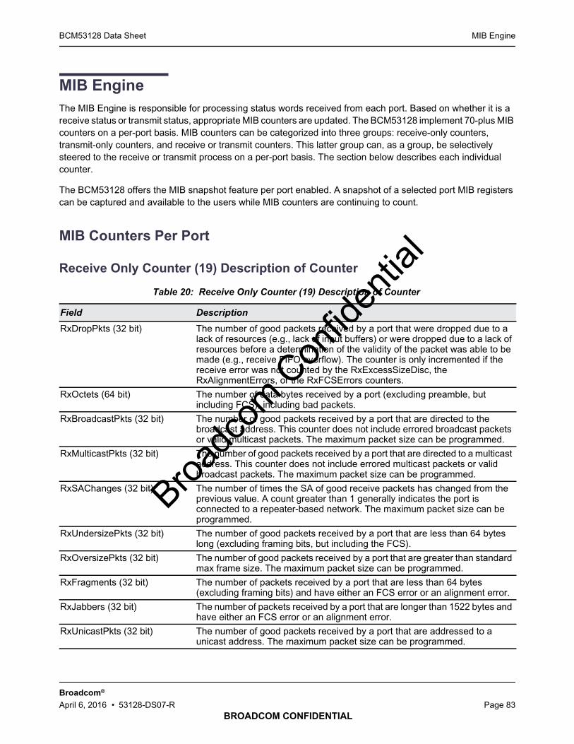
MIB EngineBCM53128 Data Sheet
BROADCOM CONFIDENTIAL
Broadcom®
April 6, 2016 • 53128-DS07-R Page 83
MIB Engine
The MIB Engine is responsible for processing status words received from each port. Based on whether it is areceive status or transmit status, appropriate MIB counters are updated. The BCM53128 implement 70-plus MIBcounters on a per-port basis. MIB counters can be categorized into three groups: receive-only counters,transmit-only counters, and receive or transmit counters. This latter group can, as a group, be selectivelysteered to the receive or transmit process on a per-port basis. The section below describes each individualcounter.
The BCM53128 offers the MIB snapshot feature per port enabled. A snapshot of a selected port MIB registerscan be captured and available to the users while MIB counters are continuing to count.
MIB Counters Per Port
Receive Only Counter (19) Description of Counter
Table 20: Receive Only Counter (19) Description of Counter
Field Description
RxDropPkts (32 bit) The number of good packets received by a port that were dropped due to alack of resources (e.g., lack of input buffers) or were dropped due to a lack ofresources before a determination of the validity of the packet was able to bemade (e.g., receive FIFO overflow). The counter is only incremented if thereceive error was not counted by the RxExcessSizeDisc, theRxAlignmentErrors, or the RxFCSErrors counters.
RxOctets (64 bit) The number of data bytes received by a port (excluding preamble, butincluding FCS), including bad packets.
RxBroadcastPkts (32 bit) The number of good packets received by a port that are directed to thebroadcast address. This counter does not include errored broadcast packetsor valid multicast packets. The maximum packet size can be programmed.
RxMulticastPkts (32 bit) The number of good packets received by a port that are directed to a multicastaddress. This counter does not include errored multicast packets or validbroadcast packets. The maximum packet size can be programmed.
RxSAChanges (32 bit) The number of times the SA of good receive packets has changed from theprevious value. A count greater than 1 generally indicates the port isconnected to a repeater-based network. The maximum packet size can beprogrammed.
RxUndersizePkts (32 bit) The number of good packets received by a port that are less than 64 byteslong (excluding framing bits, but including the FCS).
RxOversizePkts (32 bit) The number of good packets received by a port that are greater than standardmax frame size. The maximum packet size can be programmed.
RxFragments (32 bit) The number of packets received by a port that are less than 64 bytes(excluding framing bits) and have either an FCS error or an alignment error.
RxJabbers (32 bit) The number of packets received by a port that are longer than 1522 bytes andhave either an FCS error or an alignment error.
RxUnicastPkts (32 bit) The number of good packets received by a port that are addressed to aunicast address. The maximum packet size can be programmed.
Broadc
om C
onfid
entia
l
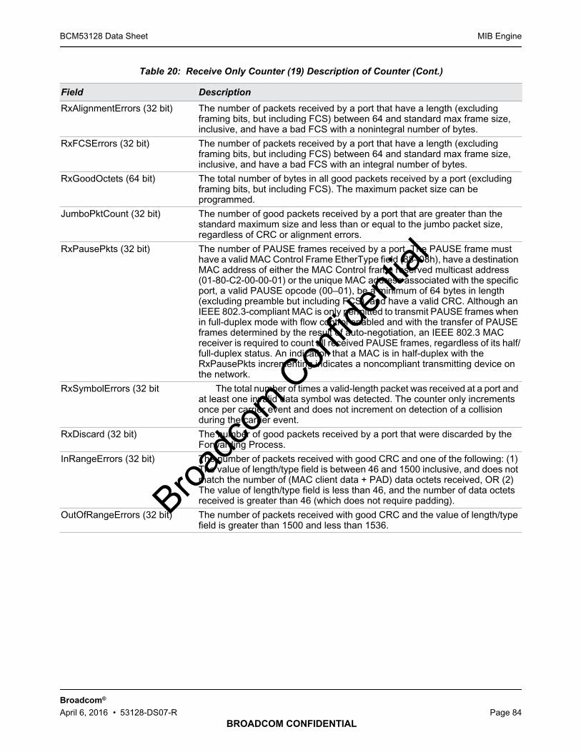
MIB EngineBCM53128 Data Sheet
BROADCOM CONFIDENTIAL
Broadcom®
April 6, 2016 • 53128-DS07-R Page 84
RxAlignmentErrors (32 bit) The number of packets received by a port that have a length (excludingframing bits, but including FCS) between 64 and standard max frame size,inclusive, and have a bad FCS with a nonintegral number of bytes.
RxFCSErrors (32 bit) The number of packets received by a port that have a length (excludingframing bits, but including FCS) between 64 and standard max frame size,inclusive, and have a bad FCS with an integral number of bytes.
RxGoodOctets (64 bit) The total number of bytes in all good packets received by a port (excludingframing bits, but including FCS). The maximum packet size can beprogrammed.
JumboPktCount (32 bit) The number of good packets received by a port that are greater than thestandard maximum size and less than or equal to the jumbo packet size,regardless of CRC or alignment errors.
RxPausePkts (32 bit) The number of PAUSE frames received by a port. The PAUSE frame musthave a valid MAC Control Frame EtherType field (88–08h), have a destinationMAC address of either the MAC Control frame reserved multicast address(01-80-C2-00-00-01) or the unique MAC address associated with the specificport, a valid PAUSE opcode (00–01), be a minimum of 64 bytes in length(excluding preamble but including FCS), and have a valid CRC. Although anIEEE 802.3-compliant MAC is only permitted to transmit PAUSE frames whenin full-duplex mode with flow control enabled and with the transfer of PAUSEframes determined by the result of auto-negotiation, an IEEE 802.3 MACreceiver is required to count all received PAUSE frames, regardless of its half/full-duplex status. An indication that a MAC is in half-duplex with theRxPausePkts incrementing indicates a noncompliant transmitting device onthe network.
RxSymbolErrors (32 bit The total number of times a valid-length packet was received at a port andat least one invalid data symbol was detected. The counter only incrementsonce per carrier event and does not increment on detection of a collisionduring the carrier event.
RxDiscard (32 bit) The number of good packets received by a port that were discarded by theForwarding Process.
InRangeErrors (32 bit) The number of packets received with good CRC and one of the following: (1)The value of length/type field is between 46 and 1500 inclusive, and does notmatch the number of (MAC client data + PAD) data octets received, OR (2)The value of length/type field is less than 46, and the number of data octetsreceived is greater than 46 (which does not require padding).
OutOfRangeErrors (32 bit) The number of packets received with good CRC and the value of length/typefield is greater than 1500 and less than 1536.
Table 20: Receive Only Counter (19) Description of Counter (Cont.)
Field Description
Broadc
om C
onfid
entia
l
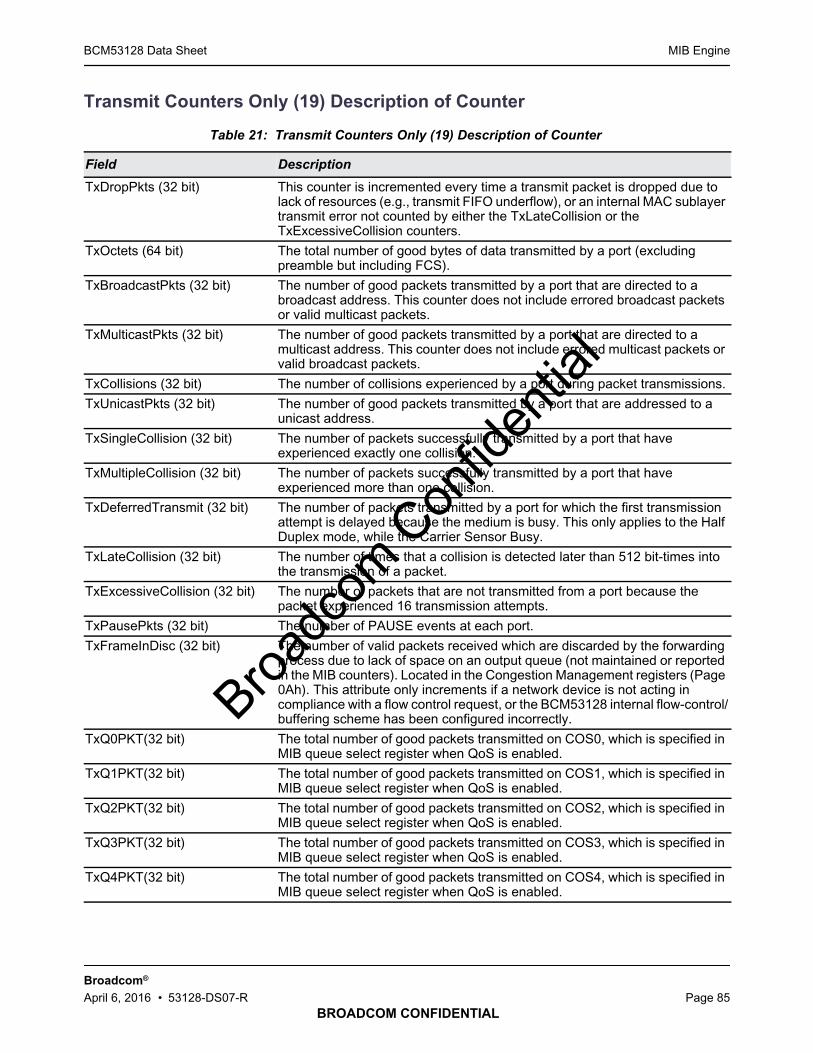
MIB EngineBCM53128 Data Sheet
BROADCOM CONFIDENTIAL
Broadcom®
April 6, 2016 • 53128-DS07-R Page 85
Transmit Counters Only (19) Description of Counter
Table 21: Transmit Counters Only (19) Description of Counter
Field Description
TxDropPkts (32 bit) This counter is incremented every time a transmit packet is dropped due tolack of resources (e.g., transmit FIFO underflow), or an internal MAC sublayertransmit error not counted by either the TxLateCollision or theTxExcessiveCollision counters.
TxOctets (64 bit) The total number of good bytes of data transmitted by a port (excludingpreamble but including FCS).
TxBroadcastPkts (32 bit) The number of good packets transmitted by a port that are directed to abroadcast address. This counter does not include errored broadcast packetsor valid multicast packets.
TxMulticastPkts (32 bit) The number of good packets transmitted by a port that are directed to amulticast address. This counter does not include errored multicast packets orvalid broadcast packets.
TxCollisions (32 bit) The number of collisions experienced by a port during packet transmissions.
TxUnicastPkts (32 bit) The number of good packets transmitted by a port that are addressed to aunicast address.
TxSingleCollision (32 bit) The number of packets successfully transmitted by a port that haveexperienced exactly one collision.
TxMultipleCollision (32 bit) The number of packets successfully transmitted by a port that haveexperienced more than one collision.
TxDeferredTransmit (32 bit) The number of packets transmitted by a port for which the first transmissionattempt is delayed because the medium is busy. This only applies to the HalfDuplex mode, while the Carrier Sensor Busy.
TxLateCollision (32 bit) The number of times that a collision is detected later than 512 bit-times intothe transmission of a packet.
TxExcessiveCollision (32 bit) The number of packets that are not transmitted from a port because thepacket experienced 16 transmission attempts.
TxPausePkts (32 bit) The number of PAUSE events at each port.
TxFrameInDisc (32 bit) The number of valid packets received which are discarded by the forwardingprocess due to lack of space on an output queue (not maintained or reportedin the MIB counters). Located in the Congestion Management registers (Page0Ah). This attribute only increments if a network device is not acting incompliance with a flow control request, or the BCM53128 internal flow-control/buffering scheme has been configured incorrectly.
TxQ0PKT(32 bit) The total number of good packets transmitted on COS0, which is specified inMIB queue select register when QoS is enabled.
TxQ1PKT(32 bit) The total number of good packets transmitted on COS1, which is specified inMIB queue select register when QoS is enabled.
TxQ2PKT(32 bit) The total number of good packets transmitted on COS2, which is specified inMIB queue select register when QoS is enabled.
TxQ3PKT(32 bit) The total number of good packets transmitted on COS3, which is specified inMIB queue select register when QoS is enabled.
TxQ4PKT(32 bit) The total number of good packets transmitted on COS4, which is specified inMIB queue select register when QoS is enabled.
Broadc
om C
onfid
entia
l

MIB EngineBCM53128 Data Sheet
BROADCOM CONFIDENTIAL
Broadcom®
April 6, 2016 • 53128-DS07-R Page 86
Transmit or Receive Counters (10) Description of Counter
The total number of counters per port is 43.
Table 23 identifies the mapping of the BCM53128 MIB counters and their generic mnemonics to the specificcounters and mnemonics for each of the key IETF MIBs that are supported. Direct mappings are defined.However, there are several additional statistics counters, which are indirectly supported that make up the fullcomplement of the counters required to fully support each MIB. These are shown in Table 24 on page 88.
Finally, Table 25 on page 89 identifies the additional counters supported by the BCM53128 and references thespecific standard or reason for the inclusion of the counter.
TxQ5PKT(32 bit) The total number of good packets transmitted on COS5, which is specified inMIB queue select register when QoS is enabled.
Table 22: Transmit or Receive Counters (10) Description of Counter
Field Description
Pkts64Octets (32 bit) The number of packets (including error packets) that are 64 bytes long.
Pkts65to127Octets (32 bit) The number of packets (including error packets) that are between 65 and 127bytes long.
Pkts128to255Octets (32 bit) The number of packets (including error packets) that are between 128 and255 bytes long.
Pkts256to511Octets (32 bit) The number of packets (including error packets) that are between 256 and 511bytes long.
Pkts512to1023Octets (32 bit) The number of packets (including error packets) that are between 512 and1023 bytes long.
Pkts1024toMaxPktOctets (32bit)
The number of packets that (include error packets) are between 1024 and thestandard maximum packet size inclusive.
Table 23: Directly Supported MIB Counters
BCM53128 MIBEthernet-Like MIBRFC 1643
Bridge MIBRFC 1493
MIB II InterfaceRFC 1213/1573
RMON MIBRFC 1757
RxDropPkts dot3StatsInternalMACReceiveErrors
dot1dTpPortInDiscards ifInDiscards –
RxOctets – – ifInOctets etherStatsOctets
RxBroadcastPkts – – ifInBroadcastPkts etherStatsBroadcastPkts
RxMulticastPkts – – ifInMulticastPkts etherStatsMulticastPkts
RxSAChanges Note 2 Note 2 Note 2 Note 2
RxUndersizePkts – – – etherStatsUndersizePkts
Table 21: Transmit Counters Only (19) Description of Counter (Cont.)
Field Description
Broadc
om C
onfid
entia
l

MIB EngineBCM53128 Data Sheet
BROADCOM CONFIDENTIAL
Broadcom®
April 6, 2016 • 53128-DS07-R Page 87
RxOversizePkts dot3StatsFrameTooLongs
– – etherStatsOverrsizePkts
RxFragments – – – eytherStatsFragments
RxJabbers – – – etherStatsJabbers
RxUnicastPkts – – ifInUcastPkts –
RxAlignmentErrors dot3StatsAlignmentErrors
– – –
RxFCSErrors dot3StatsFCSErrors – – –
RxGoodOctets – – – –
RxExcessSizeDisc Note 2 Note 2 Note 2 Note 2
RxPausePkts Note 2 Note 2 Note 2 Note 2
RxSymbolErrors Note 2 Note 2 Note 2 Note 2
Note 1 – – ifInErrors –
Note 1 – – ifInUnknownProtos –
Note 1 – dot1dTpPortInFrames – –
TxDropPkts dot3StatsInternalMACTransmitErrors
– ifOutDiscards –
TxOctets – – ifOutOctetsNote 3
–
Note 1 – dot1dTpPortOutFrames
– –
TxBroadcastPkts – – ifOutBroadcastPkts –
TxMulticastPkts – – ifOutMulticastPkts –
TxCollisions – – – etherStatsCollisions
TxUnicastPkts – – ifOutUcastPkts –
TxSingleCollision dot3StatsSingleCollisionFrames
– – –
TxMultipleCollision dot3StatsMultipleCollisionFrames
– – –
TxDeferredTransmit dot3StatsDeferredTransmissions
– – –
TxLateCollision dot3StatsLateCollision
– – –
TxExcessiveCollision dot3StatsExcessiveCollision
– – –
TxFrameInDisc Note 2 Note 2 Note 2 Note 2
TxPausePkts Note 2 Note 2 Note 2 Note 2
Note 4 dot3StatsCarrierSenseErrors
– – –
Note 1 – – ifOutErrors –
Table 23: Directly Supported MIB Counters (Cont.)
BCM53128 MIBEthernet-Like MIBRFC 1643
Bridge MIBRFC 1493
MIB II InterfaceRFC 1213/1573
RMON MIBRFC 1757
Broadc
om C
onfid
entia
l
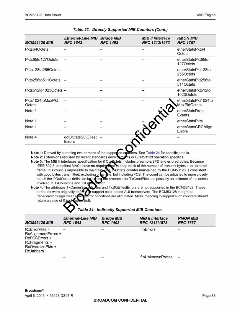
MIB EngineBCM53128 Data Sheet
BROADCOM CONFIDENTIAL
Broadcom®
April 6, 2016 • 53128-DS07-R Page 88
Note 1: Derived by summing two or more of the supported counters. See Table 24 for specific details.Note 2: Extensions required by recent standards developments or BCM53128 operation specifics.Note 3: The MIB II interfaces specification for if OutOctets includes preamble/SFD and errored bytes. Because
IEEE 802.3-compliant MACs have no requirement to keep track of the number of transmit bytes in an erroredframe, this count is impossible to maintain. The TxOctets counter maintained by the BCM53128 is consistentwith good bytes transmitted, excluding preamble, but including FCS. The count can be adjusted to more closelymatch the if OutOctets definition by adding the preamble for TxGoodPkts and possibly an estimate of the octetsinvolved in TxCollisions and TxLateCollision.
Note 4: The attributes TxCarrierSenseErrors and TxSQETestErrors are not supported in the BCM53128. Theseattributes were originally defined to support coax-based AUI transceivers. The BCM53128 integratedtransceiver design means these error conditions are eliminated. MIBs intending to support such counters shouldreturn a value of 0 (not supported).
Pkts64Octets – – – etherStatsPkt64Octets
Pkts65to127Octets – – – etherStatsPkt65to127Octets
Pkts128to255Octets – – – etherStatsPkt128to255Octets
Pkts256to511Octets – – – etherStatsPkt256to511Octets
Pkts512to1023Octets – – – etherStatsPkt512to1023Octets
Pkts1024toMaxPktOctets
– – – etherStatsPkt1024toMaxPktOctets
Note 1 – – – etherStatsDropEvents
Note 1 – – – etherStatsPkts
Note 1 – – – etherStatsCRCAlignErrors
Note 4 dot3StatsSQETestErrors
– – –
Table 24: Indirectly Supported MIB Counters
BCM53128 MIBEthernet-Like MIBRFC 1643
Bridge MIBRFC 1493
MIB II InterfaceRFC 1213/1573
RMON MIBRFC 1757
RxErrorPkts =RxAlignmentErrors +RxFCSErrors +RxFragments +RxOversizePkts +RxJabbers
– – ifInErrors –
– – ifInUnknownProtos –
Table 23: Directly Supported MIB Counters (Cont.)
BCM53128 MIBEthernet-Like MIBRFC 1643
Bridge MIBRFC 1493
MIB II InterfaceRFC 1213/1573
RMON MIBRFC 1757
Broadc
om C
onfid
entia
l
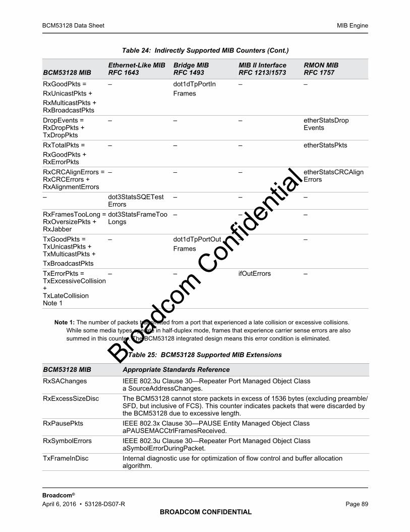
MIB EngineBCM53128 Data Sheet
BROADCOM CONFIDENTIAL
Broadcom®
April 6, 2016 • 53128-DS07-R Page 89
Note 1: The number of packets transmitted from a port that experienced a late collision or excessive collisions.While some media types operate in half-duplex mode, frames that experience carrier sense errors are alsosummed in this counter. The BCM53128 integrated design means this error condition is eliminated.
RxGoodPkts =RxUnicastPkts +RxMulticastPkts +RxBroadcastPkts
– dot1dTpPortInFrames
– –
DropEvents =RxDropPkts +TxDropPkts
– – – etherStatsDropEvents
RxTotalPkts =RxGoodPkts +RxErrorPkts
– – – etherStatsPkts
RxCRCAlignErrors =RxCRCErrors +RxAlignmentErrors
– – – etherStatsCRCAlignErrors
– dot3StatsSQETestErrors
– – –
RxFramesTooLong =RxOversizePkts +RxJabber
dot3StatsFrameTooLongs
– – –
TxGoodPkts =TxUnicastPkts +TxMulticastPkts +TxBroadcastPkts
– dot1dTpPortOutFrames
– –
TxErrorPkts =TxExcessiveCollision+TxLateCollisionNote 1
– – ifOutErrors –
Table 25: BCM53128 Supported MIB Extensions
BCM53128 MIB Appropriate Standards Reference
RxSAChanges IEEE 802.3u Clause 30—Repeater Port Managed Object Classa SourceAddressChanges.
RxExcessSizeDisc The BCM53128 cannot store packets in excess of 1536 bytes (excluding preamble/SFD, but inclusive of FCS). This counter indicates packets that were discarded bythe BCM53128 due to excessive length.
RxPausePkts IEEE 802.3x Clause 30—PAUSE Entity Managed Object ClassaPAUSEMACCtrlFramesReceived.
RxSymbolErrors IEEE 802.3u Clause 30—Repeater Port Managed Object ClassaSymbolErrorDuringPacket.
TxFrameInDisc Internal diagnostic use for optimization of flow control and buffer allocationalgorithm.
Table 24: Indirectly Supported MIB Counters (Cont.)
BCM53128 MIBEthernet-Like MIBRFC 1643
Bridge MIBRFC 1493
MIB II InterfaceRFC 1213/1573
RMON MIBRFC 1757
Broadc
om C
onfid
entia
l

Integrated High-Performance MemoryBCM53128 Data Sheet
BROADCOM CONFIDENTIAL
Broadcom®
April 6, 2016 • 53128-DS07-R Page 90
Integrated High-Performance Memory
The BCM53128 embed a 192 KB high-performance SRAM for storing packet data. This eliminates the need forexternal memory and allows for the implementation of extremely low-cost systems.
The internal RAM controller efficiently executes memory transfers and achieves nonblocking performance forstand-alone 8-port applications.
Switch Controller
The core of the BCM53128 devices is a cost-effective and high-performance switch controller. The controllermanages packet forwarding between the MAC receive and transmit ports through the frame buffer memory witha store and forward architecture. The switch controller encompasses the functions of buffer management,memory arbitration, and transmit descriptor queueing.
Buffer Management
The frame buffer memory is divided into pages (units of data consisting of 256 bytes each). Each receivedpacket may be allocated more than one page. For example, six pages are required to store a 1522-byte frame.Frame data is stored in the buffer memory as the packet is received. After reception, the frame is queued to theegress port(s) transmit queue. This list tracks the transmission of the packet. After successful packettransmission, the buffer memory is released to the free buffer pool.
Memory Arbitration
Processes requesting access to the internal memory include the receive and transmit frame data handlers,address resolution, the VLAN lookup, learning and aging functions, egress descriptor update, and output-portqueue managers. These processes are arbitrated to provide fair access to the memory and minimize the latencyof critical processes to provide a fully nonblocking solution.
Transmit Output Port Queues
Frames are maintained in the egress port using a linked list. Two levels of linked lists are used to maintain oneoutput queue (see the figure below). The first level is the TXQ linked list, and the second level is the buffer taglinked list. The TXQ linked list is used to maintain frame TC order for each port. For each frame, the buffer taglinked list is used to maintain the order of the buffer pages corresponding to each frame.
TxPausePkts The number of PAUSE events at a given port.
Table 25: BCM53128 Supported MIB Extensions (Cont.)
BCM53128 MIB Appropriate Standards Reference
Broadc
om C
onfid
entia
l
Switch ControllerBCM53128 Data Sheet
BROADCOM CONFIDENTIAL
Broadcom®
April 6, 2016 • 53128-DS07-R Page 91
Each egress port supports up to six transmit queues for servicing Quality of Service (QoS). All six transmitqueues share the 768 entries of the TXQ table. The TXQ table is maintained as a linked list, and each node inthe TXQ uses one entry in the TXQ table. The TXQ size for each priority can be programmed to up to 768entries.
When the QoS function has been turned off, the switch controller maintains one output queue for each egressport. The TXQ table is maintained in a per-port individual internal memory. Each node in the queue representsa pointer that points to a frame buffer tag. Each buffer tag includes frame information and a pointer to the nextbuffer tag. Each buffer tag has an associated page allocated in the frame buffer. For a packet with a frame sizelarger than 256 bytes, multiple buffer tags are required. For instance, a 9720-byte jumbo frame requires 38buffer tags for handling the frame.
Figure 11: TXQ and Buffer Tag Structure
Frame 0,0Frame 1,0
Empty
Frame 0,1
Empty
Frame 0,2
Frame 3,1
EmptyFrame 3,0
Priority 0
Empty
Page 0,1,0
Page 3,1,1
Page 0,2,0
Page 3,1,0
Priority 1Page 3,0,0
256B256B
256B
256B
256B
256B
256B
256B256B
TXQ Buffer Tag Data Buffer
Priority 3Priority 2
Page 0,1,1
Page 1,0,0Page 0,0,0
Broadc
om C
onfid
entia
l

System InterfacesBCM53128 Data Sheet
BROADCOM CONFIDENTIAL
Broadcom®
April 6, 2016 • 53128-DS07-R Page 92
Section 4: System Interfaces
Overview of System Interfaces
The BCM53128 include the following interfaces:
• “Copper Interface”
• “Frame Management Port Interface” on page 93
• “Configuration Pins” on page 94
• “Programming Interfaces” on page 95
• “MDC/MDIO Interface” on page 112
• “LED Interfaces” on page 119
Each interface is discussed in detail in these sections.
Copper Interface
The internal PHYs transmit and receive data using the analog copper interface. This section discusses thefollowing topics:
• “Auto-Negotiation” on page 92
• “Line-side (Remote) Loopback Mode” on page 93
• “Reverse MII Port (RvMII)” on page 93
• “GMII Port” on page 94
• “RGMII Port” on page 94
• “SPI-Compatible Programming Interface” on page 96
• “EEPROM Interface” on page 110
• “MDC/MDIO Interface Register Programming” on page 112
• “PseudoPHY” on page 113
Auto-Negotiation
The BCM53128 negotiate a mode of operation over the copper media using the auto-negotiation mechanismdefined in the IEEE 802.3u and IEEE 802.3ab specifications. When the auto-negotiation function is enabled, theBCM53128 automatically choose the mode of operation by advertising its abilities and comparing them withthose received from its link partner. The BCM53128 can be configured to advertise the following modes:
• 1000BASE-T full-duplex and/or half-duplex
• 100BASE-TX full-duplex and/or half-duplex
• 10BASE-T full-duplex and/or half-duplex
Broadc
om C
onfid
entia
l
Frame Management Port InterfaceBCM53128 Data Sheet
BROADCOM CONFIDENTIAL
Broadcom®
April 6, 2016 • 53128-DS07-R Page 93
The transceiver negotiates with its link partner and chooses the highest common operating speed and duplexmode, commonly referred to as highest common denominator (HCD). Auto-negotiation can be disabled bysoftware control, but is required for 1000BASE-T operation.
Line-side (Remote) Loopback Mode
The line-side loopback mode allows the testing of the copper interface from the link partner. This mode isenabled by setting bit 15 of the Miscellaneous Test register. The MDI receive packet is passed through the PCSand sent back out as the MDI transmit packet. The PCS receive data appears on the internal MAC interface.
Frame Management Port Interface
The dedicated frame management port provides high-speed connection to transfer management packets to anexternal management agent. For more information about frame management, see “Frame Management” onpage 79. The port is configurable to Reverse MII (RvMII), GMII, or RGMII using strap pins or softwareconfiguration.
MII Interface
The Media Independent Interface (MII) serves as a digital data interface between the BCM53128 and anexternal 10/100 Mbps management entity or a PHY entity. The BCM53128 provides a fully IEEE 802.3u-compatible MII interface.
TMII (Turbo MII) and RvTMII (Reverse TMII) Interface
The TMII and RvTMII interfaces use the same hardware interface signals as the MII interface. The TMII moderequires the SPEED setting bits in the IMP Port States Override Register (Page 00h: Address 0Eh) bits[3:2] tobe set. The TMII mode supports 200 Mbps data rate over the existing MII interface by running the interface at(up to) 50 MHz. The original MII timing is designed such that it can support 50 MHz clocking over the existingdesign.
Reverse MII Port (RvMII)
The media independent interface (MII) serves as a digital data interface between the BCM53128 and an external10/100 Mbps management entity. Reverse MII notation reflects the MII port interfacing to a MAC-based externalagent. The RvMII contains all the signals required to transmit and receive data at 100 Mbps and 10 Mbps forboth full-duplex and half-duplex operation. See Figure 12 on page 94 for connection information.
Broadc
om C
onfid
entia
l

Configuration PinsBCM53128 Data Sheet
BROADCOM CONFIDENTIAL
Broadcom®
April 6, 2016 • 53128-DS07-R Page 94
Figure 12: RvMII Port Connection
GMII Port
The Gigabit Media Independent Interface (GMII) serves as a digital data interface between the BCM53128 andan external gigabit management entity. Transmit and receive data is clocked on the rising edge of the clocks.The GMII transmits data synchronously using the TXD[7:0] and RXD[7:0] data signals.
RGMII Port
The Reduced Gigabit Media Independent Interface (RGMII) serves as a digital data interface between theBCM53128 and an external gigabit management entity. Transmit and receive data is clocked on the rising andfalling edge of the clocks. This reduces the number of data signals crossing the MAC interface without affectingthe data transmission rate. The RGMII transmits data synchronously using the TXD[3:0] and RXD[3:0] datasignals.
Configuration Pins
Initial configuration of the BCM53128 takes place during power-on/reset by loading internal control values fromhardware strap pins. The value of the pin is loaded when the reset sequence completes, and the pin transitionsto normal operation. Pull-up or pull-down resistors can be added to these pins to control the deviceconfiguration. If the pins are left floating, the default value is determined based on the internal pull-up or pull-down configuration. See “Signal Descriptions” on page 125 for more information.
MII-Compliant MAC
RXD[3:0]
Reverse MII Port
TXD[3:0]
RXC TXC
RXDV TXEN
CRS TXER
RXER and COL
TXD[3:0] RXD[3:0]
NC
TXC RXC
TXEN RXDV
TXER
RXER
NC
Broadc
om C
onfid
entia
l

Programming InterfacesBCM53128 Data Sheet
BROADCOM CONFIDENTIAL
Broadcom®
April 6, 2016 • 53128-DS07-R Page 95
Programming Interfaces
The BCM53128 can be programmed using the SPI interface or the EEPROM interface. The interfaces share acommon pin set that is configured using the CPU_EPROM_SEL strap pin. The “SPI-Compatible ProgrammingInterface” provides access for a general-purpose microcontroller, allowing read and write access to the internalBCM53128 register space. It is configured to be compatible with the Motorola Serial Peripheral Interface (SPI)protocol. Alternatively, the “EEPROM Interface” on page 110 can be connected to an external EEPROM forwriting register values upon power-up initialization.
The internal address space of the BCM53128 devices is broken into a number of pages. Each page groups alogical set of registers associated with a specific function. Each page provides a logical address space of 256bytes, although, in general, only a small portion of the address space in each page is utilized.
An explanation follows for using the serial interface with an SPI-compatible CPU (“SPI-CompatibleProgramming Interface” on page 96) or an EEPROM (“EEPROM Interface” on page 110). Either mode can beselected with the strap pin, CPU_EPROM_SEL. Either mode has access to the same register space.
Serial Flash Interface
The BCM53128 offers a serial flash interface to store program code for the internal microcontroller (8051processor). The BCM53128 detects a flash memory device automatically and downloads the memory contentsupon power-up. The main purpose of the stored code is to configure and run the power savings mode, such asGreen mode or any application that the user wishes to run that can fit in the internal 8051 memory. Theembedded 8051 microcontroller has 128 KB of SRAM and 64 KB of ROM, supports receiving and transmittingpackets, and supports interleaved ROM/RAM access. The interface comprises four signal pins: chip select(FCS), Flash clock (FCLK), Flash Serial Out (FSO), and Flash Serial In (FSI).
GPIO
BCM53128 supports up to 8 GPIO pins. These GPIO pins can be used to connect to various external devices.Upon power-up and reset, these pins become tristated. Enable GPIO pins through the GPIO Enable Registerin 8051 Memory-Mapped Registers. They can be programmed to be either input or output pins via the GPIOregisters in 8051 Memory-Mapped Registers. The internal pull-up/pull-down of GPIOs is user-configurablethrough GPIO registers setting in 8051 Memory-Mapped Registers. Refer to the BCM53128 Programmer'sReference Guide (document number 53128-PG1xx-R) for 8051 Memory-Mapped Registers detail information.Broa
dcom
Con
fiden
tial
Programming InterfacesBCM53128 Data Sheet
BROADCOM CONFIDENTIAL
Broadcom®
April 6, 2016 • 53128-DS07-R Page 96
SPI-Compatible Programming Interface
One way to access the BCM53128 internal registers is to use the serial peripheral interconnect (SPI) compatibleinterface. This four-pin interface is designed to support a fully functional, bi-directional Motorola serial peripheralinterface (SPI) for register read/write accesses. The maximum speed of operation is 25 MHz. The SPI interfaceshares pins with the EEPROM interface. To select the SPI interface, pull up or float the CPU_EPROM_SEL pin.(The internal pull-up resistor defaults SPI interface over EEPROM interface.)
The SPI is a four-pin interface consisting of:
• Device select (SS: slave select, input to BCM53128)
• Device clock (SCK: which operates at speeds up to 25 MHz, input to BCM53128)
• Data write line (MOSI: Master Out/Slave In, input to BCM53128)
• Data read line (MISO: Master In/Slave Out, output from BCM53128)
SS: Slave Select
The SS signal is used to select a slave device and to indicate the beginning of transmission. The BCM53128SPI interface operates in the clock phase one (CPHA = 1) transmission format. In this format, the SS signal isdriven active low while the SCK signal is high, and remains low throughout the transmission including multiple-byte transfers. The minimum time requirement between SS operation is 200 ns.
SCK: Serial Clock
The serial clock SCK maximum operating frequency is 25 MHz for the BCM53128 family of devices. The SCKis used to clock data into and out of the Slave ROBO device. The SCK signal is expected to remain high whenthe interface is idle. This is because the BCM53128 SPI design is based on CPOL = 1 (Clock Polarity = 1). Thisis not programmable on BCM53128. The BCM53128 is designed so that data is driving by the falling edge andsampling by the rising edge of the SCK clock. This clock is not a free-running clock, it is generated only duringa data transaction, and remains high when the clock is idle.
MOSI: Master Output Slave Input
The MOSI signal is used by the master device to transmit the data to the slave device. The data is put on thebus and is expected to be clocked in by a rising edge of the SCK clock signal. This line is used to issue acommand and to set the register page and address value of read/write operations.
Note: All the RoboSwitch™ SPI interfaces are designed to operate in slave mode. Therefore, the SCKand SS signals are driven by the external master host device when accessing the BCM53128registers. For more detailed descriptions reader may refer to the Motorola SPI spec MC68HC08AS20-Rev. 4.0.
Broadc
om C
onfid
entia
l
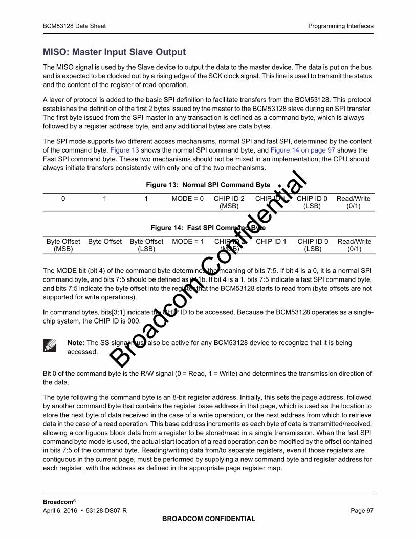
Programming InterfacesBCM53128 Data Sheet
BROADCOM CONFIDENTIAL
Broadcom®
April 6, 2016 • 53128-DS07-R Page 97
MISO: Master Input Slave Output
The MISO signal is used by the Slave device to output the data to the master device. The data is put on the busand is expected to be clocked out by a rising edge of the SCK clock signal. This line is used to transmit the statusand the content of the register of read operation.
A layer of protocol is added to the basic SPI definition to facilitate transfers from the BCM53128. This protocolestablishes the definition of the first 2 bytes issued by the master to the BCM53128 slave during an SPI transfer.The first byte issued from the SPI master in any transaction is defined as a command byte, which is alwaysfollowed by a register address byte, and any additional bytes are data bytes.
The SPI mode supports two different access mechanisms, normal SPI and fast SPI, determined by the contentof the command byte. Figure 13 shows the normal SPI command byte, and Figure 14 on page 97 shows theFast SPI command byte. These two mechanisms should not be mixed in an implementation; the CPU shouldalways initiate transfers consistently with only one of the two mechanisms.
Figure 13: Normal SPI Command Byte
Figure 14: Fast SPI Command Byte
The MODE bit (bit 4) of the command byte determines the meaning of bits 7:5. If bit 4 is a 0, it is a normal SPIcommand byte, and bits 7:5 should be defined as 011b. If bit 4 is a 1, bits 7:5 indicate a fast SPI command byte,and bits 7:5 indicate the byte offset into the register that the BCM53128 starts to read from (byte offsets are notsupported for write operations).
In command bytes, bits[3:1] indicate the CHIP ID to be accessed. Because the BCM53128 operates as a single-chip system, the CHIP ID is 000.
Bit 0 of the command byte is the R/W signal (0 = Read, 1 = Write) and determines the transmission direction ofthe data.
The byte following the command byte is an 8-bit register address. Initially, this sets the page address, followedby another command byte that contains the register base address in that page, which is used as the location tostore the next byte of data received in the case of a write operation, or the next address from which to retrievedata in the case of a read operation. This base address increments as each byte of data is transmitted/received,allowing a contiguous block data from a register to be stored/read in a single transmission. When the fast SPIcommand byte mode is used, the actual start location of a read operation can be modified by the offset containedin bits 7:5 of the command byte. Reading/writing data from/to separate registers, even if those registers arecontiguous in the current page, must be performed by supplying a new command byte and register address foreach register, with the address as defined in the appropriate page register map.
0 1 1 MODE = 0 CHIP ID 2(MSB)
CHIP ID 1 CHIP ID 0(LSB)
Read/Write(0/1)
Byte Offset(MSB)
Byte Offset Byte Offset(LSB)
MODE = 1 CHIP ID 2(MSB)
CHIP ID 1 CHIP ID 0(LSB)
Read/Write(0/1)
Note: The SS signal must also be active for any BCM53128 device to recognize that it is beingaccessed. Broa
dcom
Con
fiden
tial
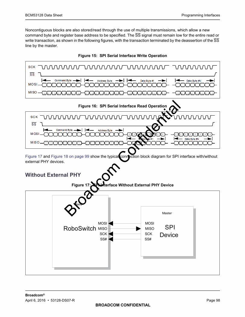
Programming InterfacesBCM53128 Data Sheet
BROADCOM CONFIDENTIAL
Broadcom®
April 6, 2016 • 53128-DS07-R Page 98
Noncontiguous blocks are also stored/read through the use of multiple transmissions, which allow a newcommand byte and register base address to be specified. The SS signal must remain low for the entire read orwrite transaction, as shown in the following figures, with the transaction terminated by the deassertion of the SSline by the master.
Figure 15: SPI Serial Interface Write Operation
Figure 16: SPI Serial Interface Read Operation
Figure 17 and Figure 18 on page 99 show the typical connection block diagram for SPI interface with/withoutexternal PHY devices.
Without External PHY
Figure 17: SPI Interface Without External PHY Device
SPI Device
MOSI
SCKSS#
MISOMOSI
SCKSS#
MISO
Master
Slave
RoboSwitch
Broadc
om C
onfid
entia
l
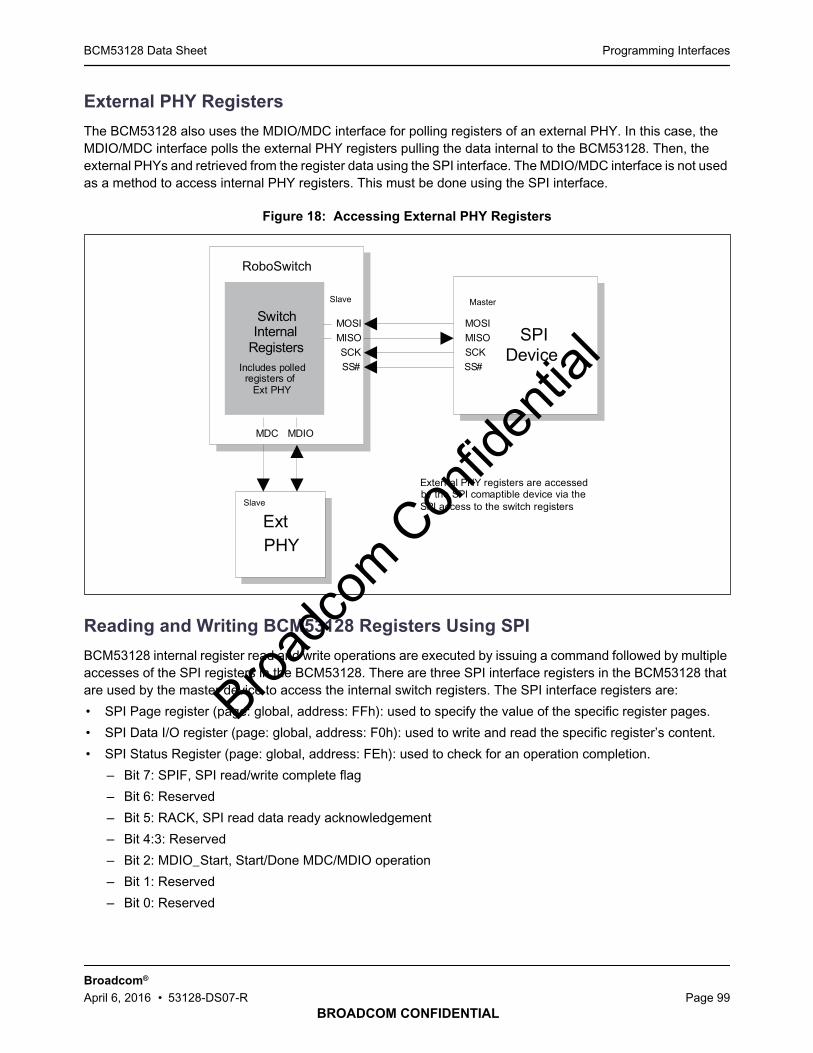
Programming InterfacesBCM53128 Data Sheet
BROADCOM CONFIDENTIAL
Broadcom®
April 6, 2016 • 53128-DS07-R Page 99
External PHY Registers
The BCM53128 also uses the MDIO/MDC interface for polling registers of an external PHY. In this case, theMDIO/MDC interface polls the external PHY registers pulling the data internal to the BCM53128. Then, theexternal PHYs and retrieved from the register data using the SPI interface. The MDIO/MDC interface is not usedas a method to access internal PHY registers. This must be done using the SPI interface.
Figure 18: Accessing External PHY Registers
Reading and Writing BCM53128 Registers Using SPI
BCM53128 internal register read and write operations are executed by issuing a command followed by multipleaccesses of the SPI registers in the BCM53128. There are three SPI interface registers in the BCM53128 thatare used by the master device to access the internal switch registers. The SPI interface registers are:
• SPI Page register (page: global, address: FFh): used to specify the value of the specific register pages.
• SPI Data I/O register (page: global, address: F0h): used to write and read the specific register’s content.
• SPI Status Register (page: global, address: FEh): used to check for an operation completion.
– Bit 7: SPIF, SPI read/write complete flag
– Bit 6: Reserved
– Bit 5: RACK, SPI read data ready acknowledgement
– Bit 4:3: Reserved
– Bit 2: MDIO_Start, Start/Done MDC/MDIO operation
– Bit 1: Reserved
– Bit 0: Reserved
SwitchSPI
Device
MOSI
SCKSS#
MISOMOSI
SCKSS#
MISO
MasterSlave
Switch Internal
RegistersIncludes polled
registers of Ext PHY
RoboSwitch
ExtPHY
MDC MDIO
Slave
External PHY registers are accessed by the SPI comaptible device via the SPI access to the switch registers.
Broadc
om C
onfid
entia
l
Programming InterfacesBCM53128 Data Sheet
BROADCOM CONFIDENTIAL
Broadcom®
April 6, 2016 • 53128-DS07-R Page 100
The BCM53128 SPI interface supports the following operating modes.
• Normal read mode
• Fast read mode
• Normal write mode
The details of each modes are described in the following paragraphs.
Normal Read Operation
Normal Read operation consists of five transactions (five SS operations):
1. Issue a Normal Read Command (opcode = 0x60) to poll the SPIF bit in the SPI Status register (0xFE) todetermine the operation can start.
2. Issue a Normal Write command (opcode = 0x61) to write the register page value into the SPI Page register0xFF.
3. Issue a Normal Read command (opcode = 0x60) to setup the required RoboSwitch register address.
4. Issue a Normal Read command (opcode = 0x60) to poll the RACK bit in the SPI status register(0xFE) todetermine the completion of read (register content gets loaded in SPI Data I/O register).
5. Issue a Normal Read command (opcode = 0x60) to read the specific registers' content placed in the SPIData I/O register (0xF0).
Note: The RoboSwitch family does not support fast-write mode.
Broadc
om C
onfid
entia
l
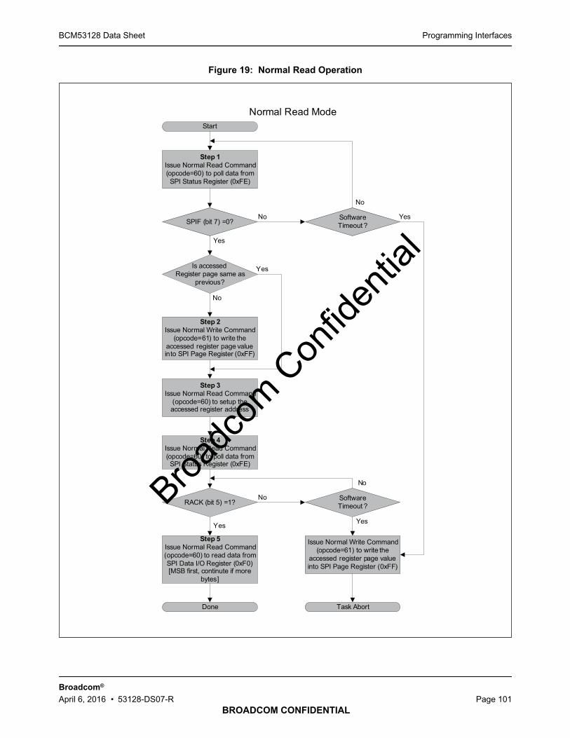
Programming InterfacesBCM53128 Data Sheet
BROADCOM CONFIDENTIAL
Broadcom®
April 6, 2016 • 53128-DS07-R Page 101
Figure 19: Normal Read Operation
Normal Read ModeStart
Step 1Issue Normal Read Command (opcode=60) to poll data from SPI Status Register (0xFE)
SPIF (bit 7) =0?
Step 2Issue Normal Write Command
(opcode=61) to write the accessed register page valueinto SPI Page Register (0xFF)
RACK (bit 5) =1?
Step 5Issue Normal Read Command (opcode=60) to read data from SPI Data I/O Register (0xF0) [MSB first, continute if more
bytes]
Yes
Yes
No
No
Done
Is accessed Register page same as
previous?
Yes
No
Step 4Issue Normal Read Command (opcode=60) to poll data from SPI Status Register (0xFE)
SoftwareTimeout ?
SoftwareTimeout ?
Task Abort
Yes
No
No
Yes
Issue Normal Write Command (opcode=61) to write the
accessed register page valueinto SPI Page Register (0xFF)
Step 3Issue Normal Read Command
(opcode=60) to setup the accessed register address
Broadc
om C
onfid
entia
l
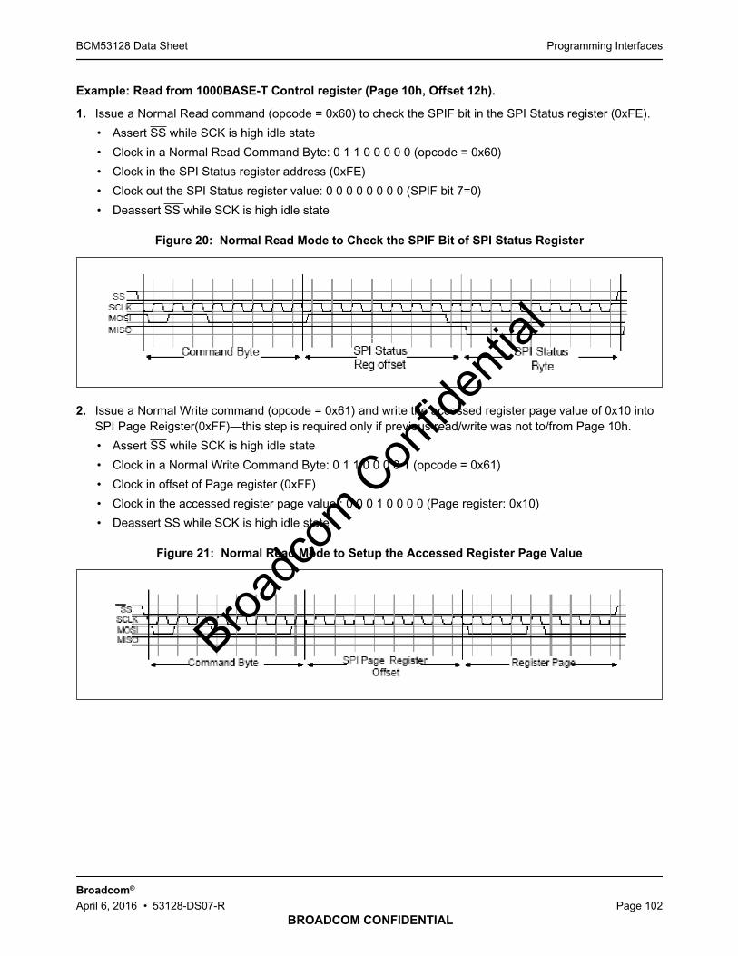
Programming InterfacesBCM53128 Data Sheet
BROADCOM CONFIDENTIAL
Broadcom®
April 6, 2016 • 53128-DS07-R Page 102
Example: Read from 1000BASE-T Control register (Page 10h, Offset 12h).
1. Issue a Normal Read command (opcode = 0x60) to check the SPIF bit in the SPI Status register (0xFE).
• Assert SS while SCK is high idle state
• Clock in a Normal Read Command Byte: 0 1 1 0 0 0 0 0 (opcode = 0x60)
• Clock in the SPI Status register address (0xFE)
• Clock out the SPI Status register value: 0 0 0 0 0 0 0 0 (SPIF bit 7=0)
• Deassert SS while SCK is high idle state
Figure 20: Normal Read Mode to Check the SPIF Bit of SPI Status Register
2. Issue a Normal Write command (opcode = 0x61) and write the accessed register page value of 0x10 intoSPI Page Reigster(0xFF)—this step is required only if previous read/write was not to/from Page 10h.
• Assert SS while SCK is high idle state
• Clock in a Normal Write Command Byte: 0 1 1 0 0 0 0 1 (opcode = 0x61)
• Clock in offset of Page register (0xFF)
• Clock in the accessed register page value,: 0 0 0 1 0 0 0 0 (Page register: 0x10)
• Deassert SS while SCK is high idle state
Figure 21: Normal Read Mode to Setup the Accessed Register Page Value
Broadc
om C
onfid
entia
l
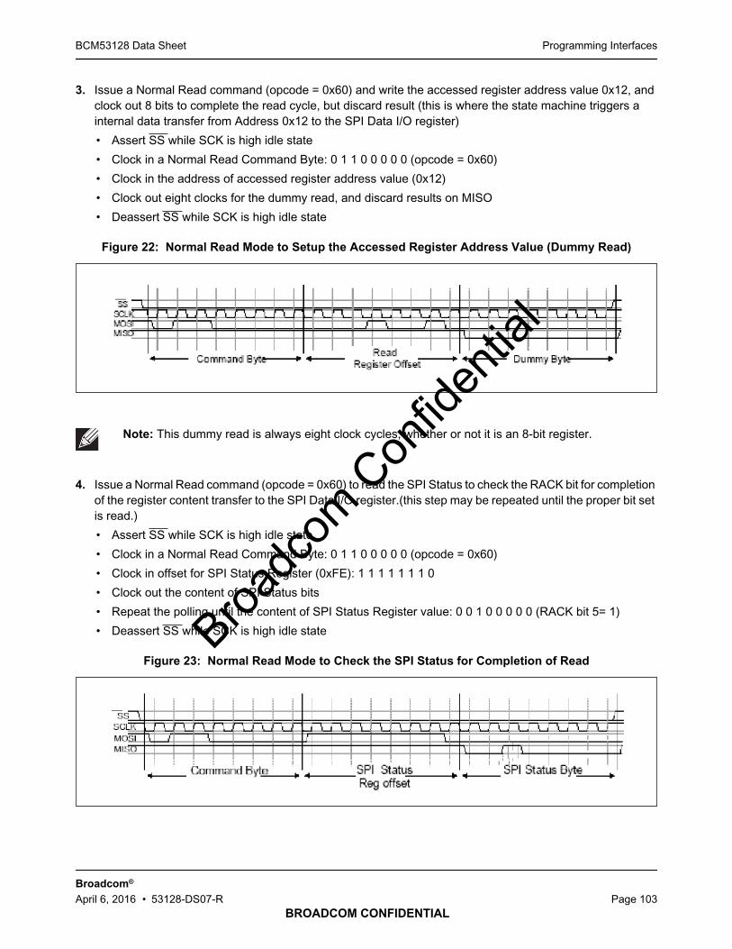
Programming InterfacesBCM53128 Data Sheet
BROADCOM CONFIDENTIAL
Broadcom®
April 6, 2016 • 53128-DS07-R Page 103
3. Issue a Normal Read command (opcode = 0x60) and write the accessed register address value 0x12, andclock out 8 bits to complete the read cycle, but discard result (this is where the state machine triggers ainternal data transfer from Address 0x12 to the SPI Data I/O register)
• Assert SS while SCK is high idle state
• Clock in a Normal Read Command Byte: 0 1 1 0 0 0 0 0 (opcode = 0x60)
• Clock in the address of accessed register address value (0x12)
• Clock out eight clocks for the dummy read, and discard results on MISO
• Deassert SS while SCK is high idle state
Figure 22: Normal Read Mode to Setup the Accessed Register Address Value (Dummy Read)
4. Issue a Normal Read command (opcode = 0x60) to read the SPI Status to check the RACK bit for completionof the register content transfer to the SPI Data I/O register.(this step may be repeated until the proper bit setis read.)
• Assert SS while SCK is high idle state
• Clock in a Normal Read Command Byte: 0 1 1 0 0 0 0 0 (opcode = 0x60)
• Clock in offset for SPI Status Register (0xFE): 1 1 1 1 1 1 1 0
• Clock out the content of SPI Status bits
• Repeat the polling until the content of SPI Status Register value: 0 0 1 0 0 0 0 0 (RACK bit 5= 1)
• Deassert SS while SCK is high idle state
Figure 23: Normal Read Mode to Check the SPI Status for Completion of Read
Note: This dummy read is always eight clock cycles, whether or not it is an 8-bit register.
Broadc
om C
onfid
entia
l

Programming InterfacesBCM53128 Data Sheet
BROADCOM CONFIDENTIAL
Broadcom®
April 6, 2016 • 53128-DS07-R Page 104
5. Issue a Normal Read command (opcode = 0x60) to read the data from the SPI Data I/O register:
• Assert SS while SCK is high idle state
• Clock in Command Byte: 0 1 1 0 0 0 0 0 (opcode = 0x60)
• Clock in offset of SPI Data I/O Register (0xF0)
• Clock out first data byte on MISO line: 0 0 0 0 0 0 0 0 (Byte 0: Bit 7 to Bit 0: MSB to LSB)
• Clock out next byte (in this case, last) on MISO line: 0 0 0 0 1 1 1 0 (Byte 1: Bit 15 to Bit 8)
• [Continue if more bytes]
• Deassert SS while SCK is high idle state
Figure 24: Normal Read Mode to Obtain the Register Content
Fast Read Operation
Fast Read operation consists of 3 transactions (three SS operations)
1. Issue a Normal Read Command (opcode = 0x60) to poll the SPIF bit in the SPI Status Register (0xFE) todetermine the operation can start.
2. Issue a Fast Read command (opcode = 0x10) to setup the accessed Register Page value into the Pageregister (0xFF).
3. Issue a Fast Read command (opcode = 0x10) to setup the accessed register address value, to trigger anactual read, and retrieve the accessed register content till the completion
Fast Read mode process is different from Normal Read mode, once the switch receives a fast read commandfollowed by the register page and address information, the status and the data (register content) will be put onthe MISO line without going through the SPI Status register or SPI Data I/O register. Once RACK bit of the bytesfollowing the Fast Read command with Address information is recognized the register content will be put onMISO line immediately following the byte with RACK bit set. The Fast Read process is described in the followingparagraphs with a flowchart followed by a step by step description.
Broadc
om C
onfid
entia
l
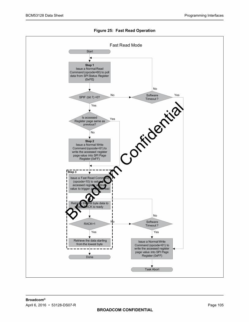
Programming InterfacesBCM53128 Data Sheet
BROADCOM CONFIDENTIAL
Broadcom®
April 6, 2016 • 53128-DS07-R Page 105
Figure 25: Fast Read Operation
Fast Read ModeStart
SPIF (bit 7) =0?
Yes
No
Step 1Issue a Normal Read
Command (opcode=60) to polldata from SPI Status Register
(0xFE)
Issue a Fast Read Command (opcode=10) to setup the accessed register address
value to trigger an actual read
Step 2Issue a Normal Write
Command (opcode=61) to write the accessed register page value into SPI Page
Register (0xFF)
Is accessed Register page same as
previous?
Yes
No
SoftwareTimeout ?
No
Yes
NoRACK=1
Retrieve the data starting from the lowest byte
Yes
Done
SoftwareTimeout ?
No
Retrieve the first byte data to check RACK is ready
Yes
Task Abort
Step 3
Issue a Normal Write Command (opcode=61) to write the accessed register page value into SPI Page
Register (0xFF)
Broadc
om C
onfid
entia
l

Programming InterfacesBCM53128 Data Sheet
BROADCOM CONFIDENTIAL
Broadcom®
April 6, 2016 • 53128-DS07-R Page 106
Example: Read from 1000BASE-T Control register (Page 10h, Offset 12h).
1. Issue a Normal Read command (opcode = 0x60) to check the SPIF bit in the SPI Status register (0xFE).
• Assert SS while SCK is high idle state
• Clock in a Normal Read Command Byte: 0 1 1 0 0 0 0 0(opcode = 0x60)
• Clock in the SPI Status register address (0xFE)
• Clock in the accessed register page value: 0 0 0 0 0 0 0 0 (SPIF bit 7=0)
• Deassert SS while SCK is high idle state
Figure 26: Normal Read Mode to Check the SPIF Bit of SPI Status Register
2. Issue a Normal Write command (opcode = 0x61) and write the accessed register page value of 0x10 in toSPI Page Reigster(0xFF) —this step is required only if previous read/write was not to/from Page 10h.
• Assert SS while SCK is high idle state
• Clock in a Fast Read Command Byte: 0 11 0 0 0 0 0 1 (opcode = 0x61)
• Clock in offset of Page register (0xFF)
• Clock in the accessed register page value: 0 0 0 1 0 0 0 0 (Page register: 0x10)
• Deassert SS while SCK is high idle state
Figure 27: Fast Read Mode to Setup New Page Value
Broadc
om C
onfid
entia
l

Programming InterfacesBCM53128 Data Sheet
BROADCOM CONFIDENTIAL
Broadcom®
April 6, 2016 • 53128-DS07-R Page 107
3. Issue a Fast Read command (opcode = 0x10), followed by the Address of the accessed register (0x12),check for a read completion by checking the RACK bit in the SPI Status register, and finally clock out theread data.
• Assert SS while SCK is high idle state
• Clock in a Fast Read Command Byte: 0 0 0 1 0 0 0 0 0 (opcode = 0x10)
• Clock in the Address of accessed register (0x12)
• Clock out Bytes Until Bit 0 or Bit 1 = 1 : 0 0 0 0 0 0 0 1 (RACK bit 0=1)
• Clock out first data byte: 0 0 0 0 0 0 0 0 (Byte 0: Bit 7 to Bit 0)
• Clock out next data (in this case, last) byte: 0 0 0 0 1 1 1 0 (Byte 1: Bit 15 to Bit 8)
• [Continue if more bytes]
• Deassert SS while SCK is high idle state
Figure 28: Fast Read to Read the Register
Normal Write Operation
Normal Write operation consists of 3 transactions (three SS operations)
1. Issue a Normal Read Command (opcode = 0x60) to poll the SPIF bit in the SPI Status register (0xFE) todetermine the operation can start.
2. Issue a Normal Write command (opcode = 0x61) to setup the accessed register page value into the pageregister (0xFF).
3. Issue a Normal Write command (opcode = 0x61) to setup the accessed register address value, followed bythe write content starting from a lower byte.
The Normal Write Mode process is described in the following paragraphs with a flowchart followed by a step bystep description.
Note: There is an errata on the RACK output timing in Fast Read mode. The RACK (bit 0) must besampled prior to toggling the clock to shift out the bit 0.
Note: The RoboSwitch does not support Fast Write Mode.
Broadc
om C
onfid
entia
l
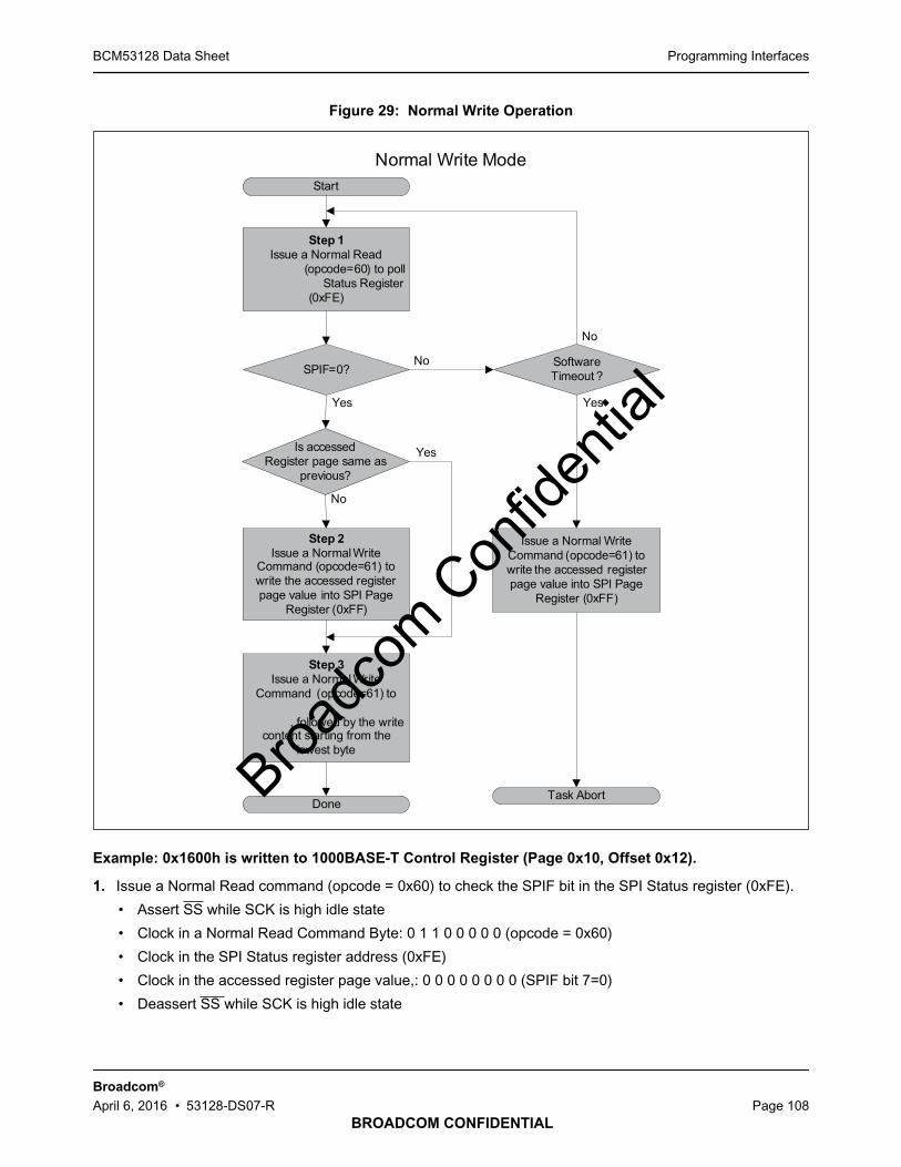
Programming InterfacesBCM53128 Data Sheet
BROADCOM CONFIDENTIAL
Broadcom®
April 6, 2016 • 53128-DS07-R Page 108
Figure 29: Normal Write Operation
Example: 0x1600h is written to 1000BASE-T Control Register (Page 0x10, Offset 0x12).
1. Issue a Normal Read command (opcode = 0x60) to check the SPIF bit in the SPI Status register (0xFE).
• Assert SS while SCK is high idle state
• Clock in a Normal Read Command Byte: 0 1 1 0 0 0 0 0 (opcode = 0x60)
• Clock in the SPI Status register address (0xFE)
• Clock in the accessed register page value,: 0 0 0 0 0 0 0 0 (SPIF bit 7=0)
• Deassert SS while SCK is high idle state
Start
Step 1Issue a Normal Read
Command (opcode=60) to polldata from SPI Status Register
(0xFE)
SPIF=0?
Step 2Issue a Normal Write
Command (opcode=61) to write the accessed register page value into SPI Page
Register (0xFF)
Step 3Issue a Normal Write
Command (opcode=61) to setup the accessed register
address, followed by the write content starting from the
lowest byte
Done
Normal Write Mode
No
Yes
Is accessed Register page same as
previous?
Yes
No
SoftwareTimeout ?
Issue a Normal Write Command (opcode=61) to write the accessed register page value into SPI Page
Register (0xFF)
Task Abort
Yes
No
Broadc
om C
onfid
entia
l
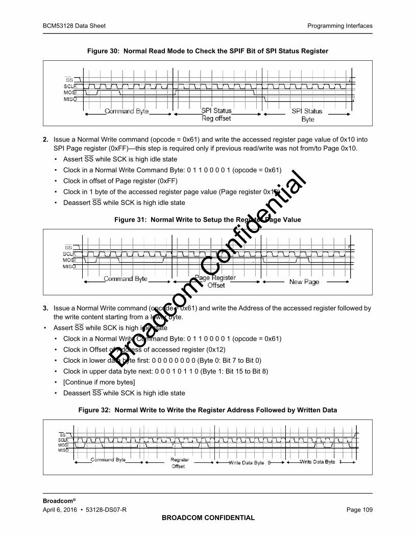
Programming InterfacesBCM53128 Data Sheet
BROADCOM CONFIDENTIAL
Broadcom®
April 6, 2016 • 53128-DS07-R Page 109
Figure 30: Normal Read Mode to Check the SPIF Bit of SPI Status Register
2. Issue a Normal Write command (opcode = 0x61) and write the accessed register page value of 0x10 intoSPI Page register (0xFF)—this step is required only if previous read/write was not from/to Page 0x10.
• Assert SS while SCK is high idle state
• Clock in a Normal Write Command Byte: 0 1 1 0 0 0 0 1 (opcode = 0x61)
• Clock in offset of Page register (0xFF)
• Clock in 1 byte of the accessed register page value (Page register 0x10)
• Deassert SS while SCK is high idle state
Figure 31: Normal Write to Setup the Register Page Value
3. Issue a Normal Write command (opcode = 0x61) and write the Address of the accessed register followed bythe write content starting from a lower byte.
• Assert SS while SCK is high idle state
• Clock in a Normal Write Command Byte: 0 1 1 0 0 0 0 1 (opcode = 0x61)
• Clock in Offset of Address of accessed register (0x12)
• Clock in lower data byte first: 0 0 0 0 0 0 0 0 (Byte 0: Bit 7 to Bit 0)
• Clock in upper data byte next: 0 0 0 1 0 1 1 0 (Byte 1: Bit 15 to Bit 8)
• [Continue if more bytes]
• Deassert SS while SCK is high idle state
Figure 32: Normal Write to Write the Register Address Followed by Written Data
Broadc
om C
onfid
entia
l
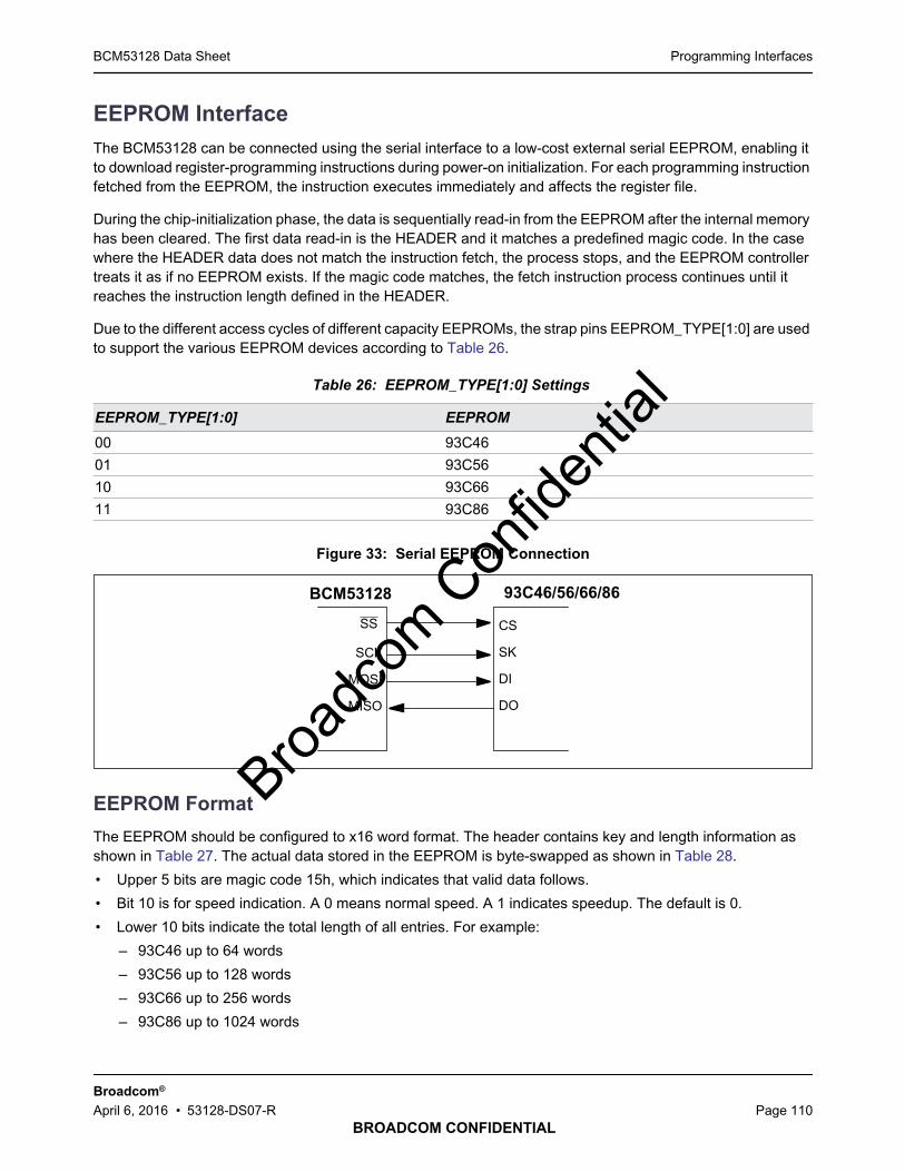
Programming InterfacesBCM53128 Data Sheet
BROADCOM CONFIDENTIAL
Broadcom®
April 6, 2016 • 53128-DS07-R Page 110
EEPROM Interface
The BCM53128 can be connected using the serial interface to a low-cost external serial EEPROM, enabling itto download register-programming instructions during power-on initialization. For each programming instructionfetched from the EEPROM, the instruction executes immediately and affects the register file.
During the chip-initialization phase, the data is sequentially read-in from the EEPROM after the internal memoryhas been cleared. The first data read-in is the HEADER and it matches a predefined magic code. In the casewhere the HEADER data does not match the instruction fetch, the process stops, and the EEPROM controllertreats it as if no EEPROM exists. If the magic code matches, the fetch instruction process continues until itreaches the instruction length defined in the HEADER.
Due to the different access cycles of different capacity EEPROMs, the strap pins EEPROM_TYPE[1:0] are usedto support the various EEPROM devices according to Table 26.
Figure 33: Serial EEPROM Connection
EEPROM Format
The EEPROM should be configured to x16 word format. The header contains key and length information asshown in Table 27. The actual data stored in the EEPROM is byte-swapped as shown in Table 28.
• Upper 5 bits are magic code 15h, which indicates that valid data follows.
• Bit 10 is for speed indication. A 0 means normal speed. A 1 indicates speedup. The default is 0.
• Lower 10 bits indicate the total length of all entries. For example:
– 93C46 up to 64 words
– 93C56 up to 128 words
– 93C66 up to 256 words
– 93C86 up to 1024 words
Table 26: EEPROM_TYPE[1:0] Settings
EEPROM_TYPE[1:0] EEPROM
00 93C46
01 93C56
10 93C66
11 93C86
SS
SCK
MOSI
MISO
BCM53128 93C46/56/66/86
CS
SK
DI
DO
Broadc
om C
onfid
entia
l
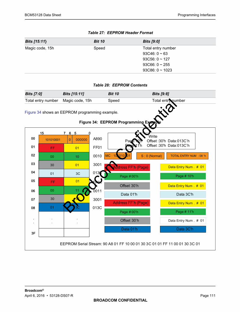
Programming InterfacesBCM53128 Data Sheet
BROADCOM CONFIDENTIAL
Broadcom®
April 6, 2016 • 53128-DS07-R Page 111
Figure 34 shows an EEPROM programming example.
Figure 34: EEPROM Programming Example
Table 27: EEPROM Header Format
Bits [15:11} Bit 10 Bits [9:0]
Magic code, 15h Speed Total entry number93C46: 0 ~ 6393C56: 0 ~ 12793C66: 0 ~ 25593C86: 0 ~ 1023
Table 28: EEPROM Contents
Bits [7:0] Bits [15:11] Bit 10 Bits [9:8]
Total entry number Magic code, 15h Speed Total entry number
101010101
FF 01
00 02
06 01
43 21
.
...
00
01
02
03
04
05
07
08
.
.
3F
0715
MC : TOTAL ENTRY NUM
22 1106
0 000010
56
66
Address FF’h (Page)
Data 01'h
MC : 101010101
101010001
FF 01
00 10
30 01
01 3C
FF 01
30
.
...
00
01
02
03
04
05
07
08
.
.
3F
0715
TOTAL ENTRY NUM
00 1106
0 000000Write
Page:10'h Offset :30'h Data:013C’hPage:11'h Offset :30'h Data:013C’h
56
01 3C
Data Entry Num . # 01
Data 3C'h
Page # 10'h
A890
FF01
0010
3001
EEPROM Serial Stream: 90 A8 01 FF 10 00 01 30 3C 01 01 FF 11 00 01 30 3C 01
Page # 00'h
Offset 30’h Data Entry Num . # 01
Address FF’h (Page)01
Page # 11'hPage # 00'h
Data 01'h Data 3C'h
Offset 30’h Data Entry Num . # 01
013C
FF01
0011
3001
013CData Entry Num . # 01
S : 0 (Normal) : 08 'h
Broadc
om C
onfid
entia
l
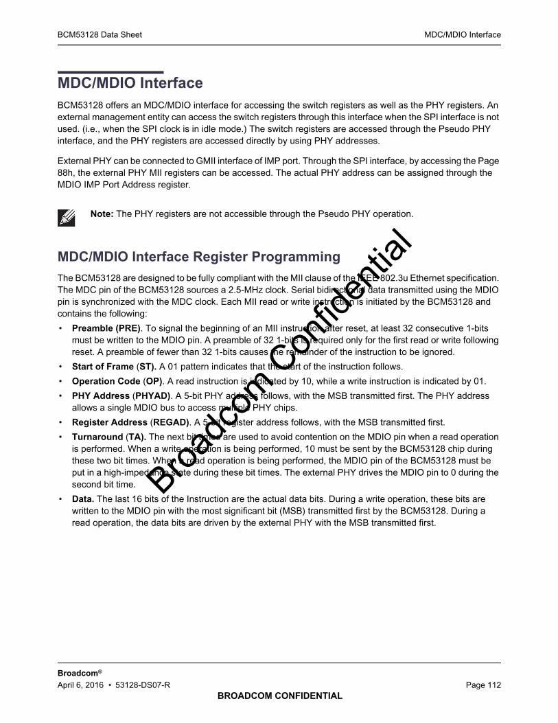
MDC/MDIO InterfaceBCM53128 Data Sheet
BROADCOM CONFIDENTIAL
Broadcom®
April 6, 2016 • 53128-DS07-R Page 112
MDC/MDIO Interface
BCM53128 offers an MDC/MDIO interface for accessing the switch registers as well as the PHY registers. Anexternal management entity can access the switch registers through this interface when the SPI interface is notused. (i.e., when the SPI clock is in idle mode.) The switch registers are accessed through the Pseudo PHYinterface, and the PHY registers are accessed directly by using PHY addresses.
External PHY can be connected to GMII interface of IMP port. Through the SPI interface, by accessing the Page88h, the external PHY MII registers can be accessed. The actual PHY address can be assigned through theMDIO IMP Port Address register.
MDC/MDIO Interface Register Programming
The BCM53128 are designed to be fully compliant with the MII clause of the IEEE 802.3u Ethernet specification.The MDC pin of the BCM53128 sources a 2.5-MHz clock. Serial bidirectional data transmitted using the MDIOpin is synchronized with the MDC clock. Each MII read or write instruction is initiated by the BCM53128 andcontains the following:
• Preamble (PRE). To signal the beginning of an MII instruction after reset, at least 32 consecutive 1-bitsmust be written to the MDIO pin. A preamble of 32 1-bits is required only for the first read or write followingreset. A preamble of fewer than 32 1-bits causes the remainder of the instruction to be ignored.
• Start of Frame (ST). A 01 pattern indicates that the start of the instruction follows.
• Operation Code (OP). A read instruction is indicated by 10, while a write instruction is indicated by 01.
• PHY Address (PHYAD). A 5-bit PHY address follows, with the MSB transmitted first. The PHY addressallows a single MDIO bus to access multiple PHY chips.
• Register Address (REGAD). A 5-bit register address follows, with the MSB transmitted first.
• Turnaround (TA). The next bit times are used to avoid contention on the MDIO pin when a read operationis performed. When a write operation is being performed, 10 must be sent by the BCM53128 chip duringthese two bit times. When a read operation is being performed, the MDIO pin of the BCM53128 must beput in a high-impedance state during these bit times. The external PHY drives the MDIO pin to 0 during thesecond bit time.
• Data. The last 16 bits of the Instruction are the actual data bits. During a write operation, these bits arewritten to the MDIO pin with the most significant bit (MSB) transmitted first by the BCM53128. During aread operation, the data bits are driven by the external PHY with the MSB transmitted first.
Note: The PHY registers are not accessible through the Pseudo PHY operation.
Broadc
om C
onfid
entia
l
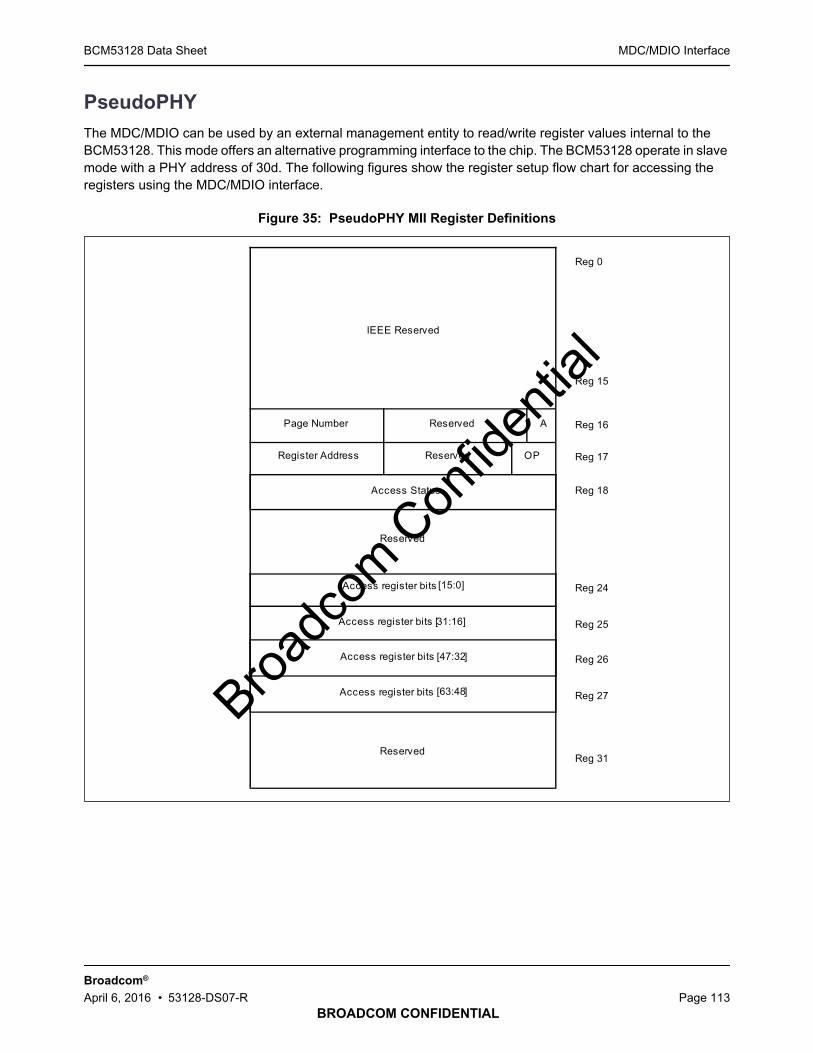
MDC/MDIO InterfaceBCM53128 Data Sheet
BROADCOM CONFIDENTIAL
Broadcom®
April 6, 2016 • 53128-DS07-R Page 113
PseudoPHY
The MDC/MDIO can be used by an external management entity to read/write register values internal to theBCM53128. This mode offers an alternative programming interface to the chip. The BCM53128 operate in slavemode with a PHY address of 30d. The following figures show the register setup flow chart for accessing theregisters using the MDC/MDIO interface.
Figure 35: PseudoPHY MII Register Definitions
IEEE Reserved
Page Number Reserved A
Register Address Reserved OP
Access Status
Reserved
Reserved
Access register bits [15:0]
Access register bits [31:16]
Access register bits [47:32]
Access register bits [63:48]
Reg 0
Reg 15
Reg 16
Reg 17
Reg 18
Reg 24
Reg 25
Reg 26
Reg 27
Reg 31
Broadc
om C
onfid
entia
l
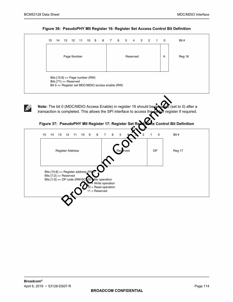
MDC/MDIO InterfaceBCM53128 Data Sheet
BROADCOM CONFIDENTIAL
Broadcom®
April 6, 2016 • 53128-DS07-R Page 114
Figure 36: PseudoPHY MII Register 16: Register Set Access Control Bit Definition
Figure 37: PseudoPHY MII Register 17: Register Set Read/Write Control Bit Definition
Note: The bit 0 (MDC/MDIO Access Enable) in register 16 should be released (set to 0) after atransaction is completed. This allows the SPI interface to access the switch register if required.
Page Number Reserved A Reg 16
15 14 13 12 11 10 9 8 7 6 5 4 3 2 1 0 Bit #
Bits [15:8] => Page number (RW)Bits [71] => ReservedBit 0 => Register set MDC/MDIO access enable (RW)
Register Address Reserved OP Reg 17
15 14 13 12 11 10 9 8 7 6 5 4 3 2 1 0 Bit #
Bits [15:8] => Register address (RW)Bits [7:2] => ReservedBits [1:0] => OP code (RW/SC),00 = No operation
01 = Write operation10 = Read operation11 = Reserved
Broadc
om C
onfid
entia
l

MDC/MDIO InterfaceBCM53128 Data Sheet
BROADCOM CONFIDENTIAL
Broadcom®
April 6, 2016 • 53128-DS07-R Page 115
Figure 38: PseudoPHY MII Register 18: Register Access Status Bit Definition
Figure 39: PseudoPHY MII Register 24: Access Register Bit Definition
Figure 40: PseudoPHY MII Register 25: Access Register Bit Definition
Reserved P Reg 18
15 14 13 12 11 10 9 8 7 6 5 4 3 2 1 0 Bit #
Bits [15:1] => ReservedBit 1 => Operation Error (RO/LH), when op_code = 2'b11, this bit is set to show operation error.Bit 0 => Prohibit Access (RO/LH), for Page Number = 8'h1X, which are PHY MII registers.
E
Access register bits [15:0] Reg 24
15 14 13 12 11 10 9 8 7 6 5 4 3 2 1 0 Bit #
Bits [15:0] => Access register bits [15:0] (RW)
Access register bits [31:16] Reg 25
15 14 13 12 11 10 9 8 7 6 5 4 3 2 1 0 Bit #
Bits [15:0] => Access register bits [31:16] (RW)
Broadc
om C
onfid
entia
l
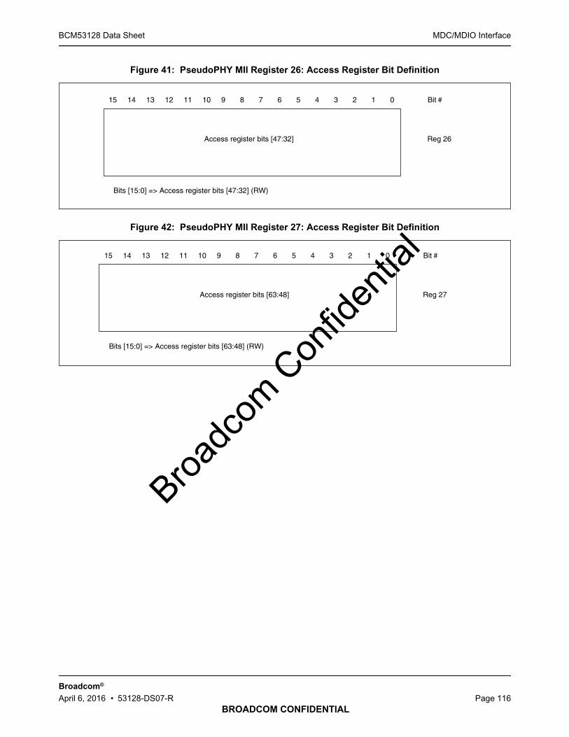
MDC/MDIO InterfaceBCM53128 Data Sheet
BROADCOM CONFIDENTIAL
Broadcom®
April 6, 2016 • 53128-DS07-R Page 116
Figure 41: PseudoPHY MII Register 26: Access Register Bit Definition
Figure 42: PseudoPHY MII Register 27: Access Register Bit Definition
Access register bits [47:32] Reg 26
15 14 13 12 11 10 9 8 7 6 5 4 3 2 1 0 Bit #
Bits [15:0] => Access register bits [47:32] (RW)
Access register bits [63:48] Reg 27
15 14 13 12 11 10 9 8 7 6 5 4 3 2 1 0 Bit #
Bits [15:0] => Access register bits [63:48] (RW)
Broadc
om C
onfid
entia
l
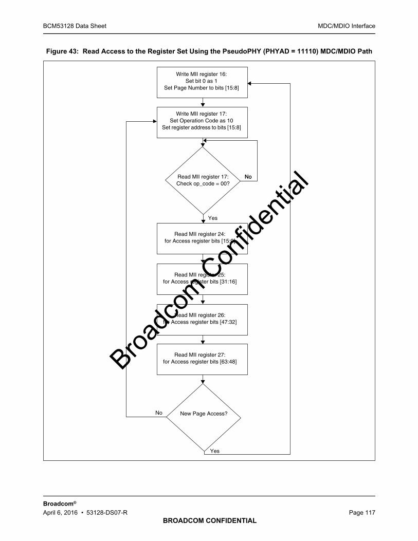
MDC/MDIO InterfaceBCM53128 Data Sheet
BROADCOM CONFIDENTIAL
Broadcom®
April 6, 2016 • 53128-DS07-R Page 117
Figure 43: Read Access to the Register Set Using the PseudoPHY (PHYAD = 11110) MDC/MDIO Path
Write MII register 16:Set bit 0 as 1
Set Page Number to bits [15:8]
Write MII register 17:Set Operation Code as 10
Set register address to bits [15:8]
Read MII register 24:for Access register bits [15:0]
Read MII register 17:Check op_code = 00?
Read MII register 25:for Access register bits [31:16]
Read MII register 26:for Access register bits [47:32]
Read MII register 27:for Access register bits [63:48]
No
Yes
Yes
New Page Access?
No
No
Broadc
om C
onfid
entia
l
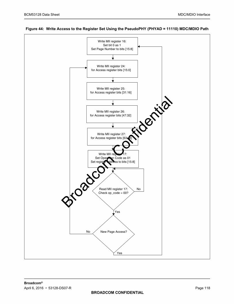
MDC/MDIO InterfaceBCM53128 Data Sheet
BROADCOM CONFIDENTIAL
Broadcom®
April 6, 2016 • 53128-DS07-R Page 118
Figure 44: Write Access to the Register Set Using the PseudoPHY (PHYAD = 11110) MDC/MDIO Path
Write MII register 16:Set bit 0 as 1
Set Page Number to bits [15:8]
Read MII register 17:Check op_code = 00?
Write MII register 25:for Access register bits [31:16]
Write MII register 26:for Access register bits [47:32]
Write MII register 27:for Access register bits [63:48]
Yes
Yes
New Page Access?
No
No
Write MII register 24:for Access register bits [15:0]
Write MII register 17:Set Operation Code as 01
Set register address to bits [15:8]
Broadc
om C
onfid
entia
l

LED InterfacesBCM53128 Data Sheet
BROADCOM CONFIDENTIAL
Broadcom®
April 6, 2016 • 53128-DS07-R Page 119
Table 29 summarizes the complete management frame format.
See “MDC/MDIO Interface” on page 112 for more information regarding the timing requirements.
LED Interfaces
The BCM53128 provides flexible visibility per-port status of various functions. The LED Interface offers an optionto display different functions for each port given the number of LED bits available. The BCM53128 provides atotal of 32 LED pins. In a 5-port switch application, these are dedicated as four LED pins per port as shown inTable 30 on page 120. If one or more ports are not used in an application and are disabled using LED EnableMap register (Page 00h: Address 16h), and no more than four LED pins are to be used per port, the locationsof the pins for the enabled ports are the same as if all eight ports were used, with four pins reserved per port,regardless of whether the port is enabled.
For example, if Port7~2 LED displays are disabled (value of register page 00h, address 16h = 0003), Port0 andPort1 LED display are still from LED pins LEDP28~31 (Port0), LEDP24~27 (Port1), just as if all eight ports wereused. If Port1 and Port0 LED displays are disabled (value of register page 00h, address 16h = 00FC), Port5,Port6, and Port7 are still from LED pins LEDP8~11 (Port5), LEDP4~7 (Port6), and LEDP0~3 (Port7), also justas if all eight ports were used.
To set up the LED interface, configure strap pins LED_MODE[1:0] or select the desired display the functions inthe LED Function 0 Control register/LED Function 1 Control register. The per-port LED display is fixed with fourfunctions.
• To configure the strap pins, set the predefined functions to be displayed by setting the strap pinsLED_MODE[1:0]. The predefined functions are described in “Signal Descriptions” on page 125. Per-portLED display is fixed four functions and occupy four LED pins.
• To configure LED display function in the two LED Function Control registers, assign each port to one of theLED Function 0 Control register and LED Function 1 Control register by enabling the bits in the LEDFunction Map register. The LED interface shifts out the status of the selected functions for ports enabled inthe LED Enable Map register.
Only four or less than four functions can be selected, and the per-port LED display occupies four LED pins (fixedfour functions). For example, if LED display function using LED Function 1 Control register is configured and thevalue is set to 0324h (four LED functions) or 0320h (three LED functions), the per-port LED display has fourfixed functions and occupies four LED pins per port, Port7 (LEDP0~3), Port6 (LEDP4~7), ....Port0(LEDP28~31).
The status of enabled ports is sent out from a higher port number to the lowest port number. The output orderthat is in the shift out is from LEDP[0], LEDP[1], LEDP[2],…..LEDP[31]. The output port order for LED is fromhigh port number to low port number, and the output bit order within the port LED is form MSB to LSB.
Table 29: MII Management Frame Format
Operation PRE ST OP PHYAD REGAD TA Data Direction
Read 1 ... 1 01 10 AAAAA RRRRR ZZZ0
Z ... ZD ... D
Driven by masterDriven by slave
Write 1 ... 1 01 01 AAAAA RRRRR 10 D ... D Driven to master
Broadc
om C
onfid
entia
l
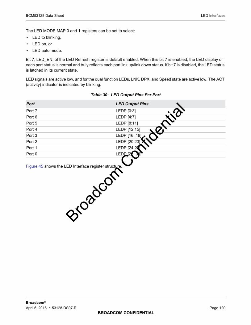
LED InterfacesBCM53128 Data Sheet
BROADCOM CONFIDENTIAL
Broadcom®
April 6, 2016 • 53128-DS07-R Page 120
The LED MODE MAP 0 and 1 registers can be set to select:
• LED to blinking,
• LED on, or
• LED auto mode.
Bit 7, LED_EN, of the LED Refresh register is default enabled. When this bit 7 is enabled, the LED display ofeach port status is normal and truly reflects each port link up/link down status. If bit 7 is disabled, the LED statusis latched in its current state.
LED signals are active low, and for the dual function LEDs, LNK, DPX, and Speed state are active low. The ACT(activity) indicator is indicated by blinking.
Figure 45 shows the LED Interface register structure.
Table 30: LED Output Pins Per Port
Port LED Output Pins
Port 7 LEDP [0:3]
Port 6 LEDP [4:7]
Port 5 LEDP [8:11]
Port 4 LEDP [12:15]
Port 3 LEDP [16: 19]
Port 2 LEDP [20:23]
Port 1 LEDP [24:27]
Port 0 LEDP [28: 31]
Broadc
om C
onfid
entia
l

LED InterfacesBCM53128 Data Sheet
BROADCOM CONFIDENTIAL
Broadcom®
April 6, 2016 • 53128-DS07-R Page 121
Figure 45: LED Interface Register Structure Diagram
The BCM53128 offers two LED Interfaces, Parallel LED Interface and Serial Interface. As shown in Figure 46on page 122, the source of LED status stream is the same for both interfaces; the status bit stream is based onthe programmed register settings. The Parallel LED Interface provides all the shifting and storing of the statusinternally, so that it does not require any external shift registers, but it requires more I/O pins to be connectedon the part.
The Serial LED Interface is being output through two pins (LEDDATA, LEDCLK). It saves the number of I/O pins,but it requires the user to design in the external shift registers.
LED Function Control Register 0
Selected FunctionsAvailable Functions
Reserved
Reserved
Reserved
LED Function Map Register
LED Enable Map Register
Port Mode Map 0 Register 0 1 0 1
Port Mode Map 1 Register 0 0 1 1
Port / Bit #7 6 5 4 3 2 1 0
0 0 1 0 1 1 0 0
1 1 1 1 1 1 0 0
1 1 1 0 1 0 1 1
1 0 0 1 1 1 0 0
15 : Reserved14 : BroadSync HD Link13 : 1G/ACT12 : 10/100M/ACT
11 : 100M/ACT10 : 10M/ACT9 : SPD1G8 : SPDI00M7 : SPD10M6 : DPX/COL5 : LNK/ACT4 : COL3 : ACT2 : DPX1 : LNK0 : Reserved
LED Function Control Register 1
Selected FunctionsAvailable Functions
15 : Reserved14 : BroadSync HD Link13 : 1G/ACT12 : 10/100M/ACT
11 : 100M/ACT10 : 10M/ACT9 : SPD1G8 : SPDI00M7 : SPD10M6 : DPX/COL5 : LNK/ACT4 : COL3 : ACT2 : DPX1 : LNK0 : Reserved
1G/ACTLNKL/ACTGDPX/COL
LNK LNKG/ACTLSPD100M
LED OFFLED ONLED BLINKLED AUTO
Broadc
om C
onfid
entia
l
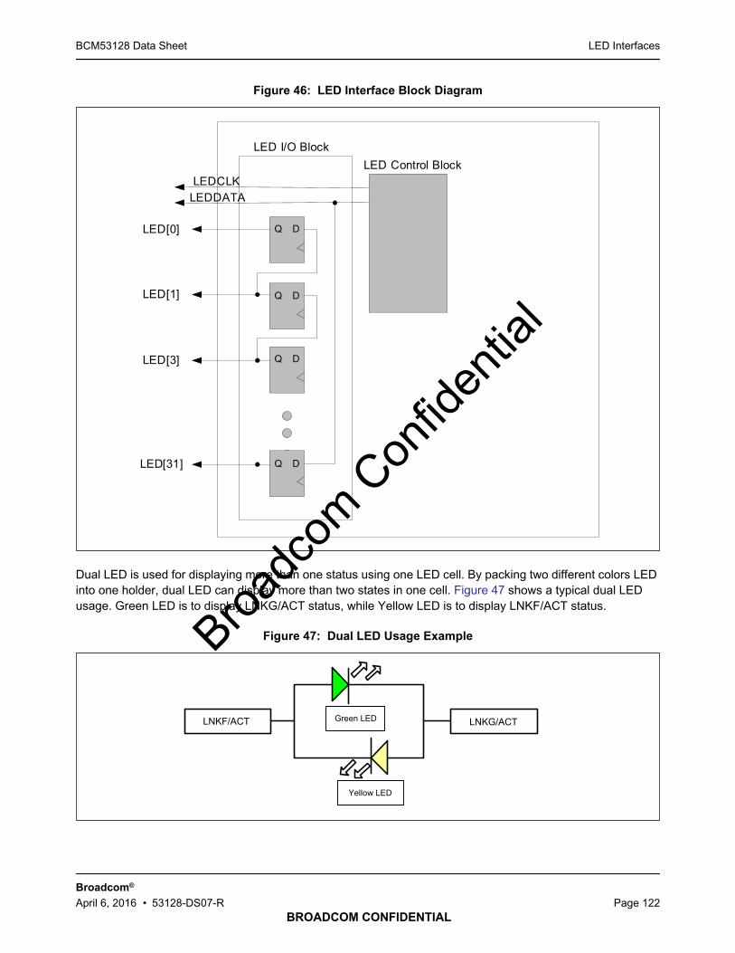
LED InterfacesBCM53128 Data Sheet
BROADCOM CONFIDENTIAL
Broadcom®
April 6, 2016 • 53128-DS07-R Page 122
Figure 46: LED Interface Block Diagram
Dual LED is used for displaying more than one status using one LED cell. By packing two different colors LEDinto one holder, dual LED can display more than two states in one cell. Figure 47 shows a typical dual LEDusage. Green LED is to display LNKG/ACT status, while Yellow LED is to display LNKF/ACT status.
Figure 47: Dual LED Usage Example
Q D
Q D
Q D
LEDCLKLEDDATA
LED[0]
LED[1]
LED[3]
LED Control BlockLED I/O Block
Q DLED[31]
LNKF/ACT LNKG/ACTGreen LED
Yellow LED
Broadc
om C
onfid
entia
l
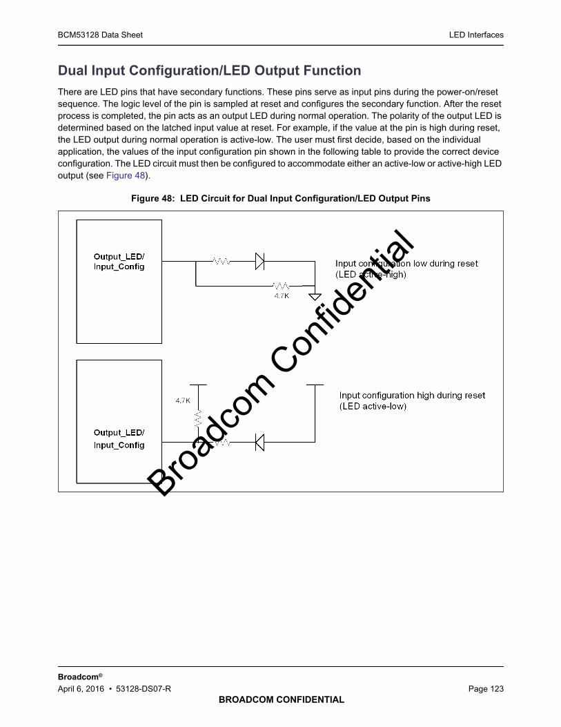
LED InterfacesBCM53128 Data Sheet
BROADCOM CONFIDENTIAL
Broadcom®
April 6, 2016 • 53128-DS07-R Page 123
Dual Input Configuration/LED Output Function
There are LED pins that have secondary functions. These pins serve as input pins during the power-on/resetsequence. The logic level of the pin is sampled at reset and configures the secondary function. After the resetprocess is completed, the pin acts as an output LED during normal operation. The polarity of the output LED isdetermined based on the latched input value at reset. For example, if the value at the pin is high during reset,the LED output during normal operation is active-low. The user must first decide, based on the individualapplication, the values of the input configuration pin shown in the following table to provide the correct deviceconfiguration. The LED circuit must then be configured to accommodate either an active-low or active-high LEDoutput (see Figure 48).
Figure 48: LED Circuit for Dual Input Configuration/LED Output Pins
Broadc
om C
onfid
entia
l

Hardware Signal Definition TableBCM53128 Data Sheet
BROADCOM CONFIDENTIAL
Broadcom®
April 6, 2016 • 53128-DS07-R Page 124
Section 5: Hardware Signal Definit ionTable
I/O Signal Types
The following conventions are used to identify the I/O types shown in Table 31. The I/O pin type is useful inreferencing the DC-pin characteristics.
Table 31: I/O Signal Type Definitions
Abbreviation Description
XYZ Active low signal
A Analog pin type
B Bias pin type
CS Continuously sampled
D Digital pin type
DNC Do not connect
GND Ground
I Input
I/O Bidirectional
IPU Input with internal pull-up
O3S Tristated Signal
ODO Open-drain output
O Output
OPU Output with internal pull-up
OPD Output with internal pull-down
PD Internal pull-down
SOR Sample on reset
PWR Power pin supply
PU Internal pull-up
XT Crystal pin type
Broadc
om C
onfid
entia
l
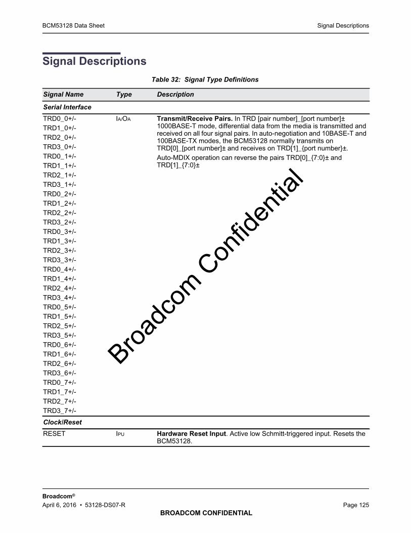
Signal DescriptionsBCM53128 Data Sheet
BROADCOM CONFIDENTIAL
Broadcom®
April 6, 2016 • 53128-DS07-R Page 125
Signal Descriptions
Table 32: Signal Type Definitions
Signal Name Type Description
Serial Interface
TRD0_0+/-TRD1_0+/-TRD2_0+/-TRD3_0+/-TRD0_1+/-TRD1_1+/-TRD2_1+/-TRD3_1+/-TRD0_2+/-TRD1_2+/-TRD2_2+/-TRD3_2+/-TRD0_3+/-TRD1_3+/-TRD2_3+/-TRD3_3+/-TRD0_4+/-TRD1_4+/-TRD2_4+/-TRD3_4+/-TRD0_5+/-TRD1_5+/-TRD2_5+/-TRD3_5+/-TRD0_6+/-TRD1_6+/-TRD2_6+/-TRD3_6+/-TRD0_7+/-TRD1_7+/-TRD2_7+/-TRD3_7+/-
IA/OA Transmit/Receive Pairs. In TRD [pair number]_[port number]±1000BASE-T mode, differential data from the media is transmitted andreceived on all four signal pairs. In auto-negotiation and 10BASE-T and100BASE-TX modes, the BCM53128 normally transmits onTRD[0]_[port number]± and receives on TRD[1]_{port number}±.Auto-MDIX operation can reverse the pairs TRD[0]_{7:0}± andTRD[1]_{7:0}±
Clock/Reset
RESET IPU Hardware Reset Input. Active low Schmitt-triggered input. Resets theBCM53128.
Broadc
om C
onfid
entia
l

Signal DescriptionsBCM53128 Data Sheet
BROADCOM CONFIDENTIAL
Broadcom®
April 6, 2016 • 53128-DS07-R Page 126
XTALI IXT 25 MHz Crystal Oscillator Input/Output. A continuous 25 MHzreference clock must be supplied to the BCM53128 by connecting a 25MHz crystal between these two pins or by driving XTALI with an external25 MHz oscillator clock. When using a crystal, connect a loadingcapacitor from each pin to GND. When using an oscillator, leave XTALOunconnected.
XTALO OXT
IMP Interface
IMP_TXCLK I/O MII/TMII Transmit Clock. This is an input pin in MII mode, or GMII modebut speed is 100Mbps/10Mbps. It synchronizes the TXD[3:0] andconnects to the PHY Entity TXC. In 100 Mbps mode, this is 25 MHz, andin 10 Mbps mode, this is 2.5 MHz. In 200 Mbps mode (TMII), this is 50MHz.RvMII/RvTMII Receive Clock. This is an output pin in RvMII mode. Itsynchronizes the TXD[3:0] in RvMII mode and connects to the MAC/Management Entity RXC. In 100 Mbps mode, this is 25 MHz, and in 10Mbps mode, this is 2.5 MHz. In 200 Mbps mode (RvTMII), this is 50MHz. This output pin has an internal 25 -series termination resistor.This clock is not use in the other conditions.
IMP_TXD[3:0] O GMII Transmit Data Output (first nibble). Data bits TXD[3:0] areclocked on the rising edge of TXCLK.RGMII Transmit Data Output. For 1000 Mbps operation, data bitsTXD[3:0] are clocked on the rising edge of TXCLK, and data bitsTXD[7:4] are clocked on the falling edge of TXCLK. For 10 Mbps and100 Mbps, data bits TXD[3:0] are clocked on the rising edge of TXCLK.RvMII/RvTMII Receive Data Output. Clocked on the rising edge ofTXCLK and connected to the RXD pins of the external MAC/Management entity.MII/TMII Transmit Data Output. Clocked on the rising edge of TXCLKsupplied by MAC/Management entity.These output pins have internal 25 -series termination resistor.
IMP_TXD[7:4] O GMII Transmit Data Output (second nibble). Data bits [7:4] areclocked on the rising edge of TXCLK. These output pins have internal25 -series termination resistor.
IMP_TXEN O GMII/MII/TMII Transmit Enable. Active high. TXEN indicates the dataon the TXD pins are encoded and transmitted.RGMII Transmit Control. On the rising edge of TXCLK, TXEN indicatesthat a transmit frame is in progress, and the data present on theTXD[3:0] output pins is valid. On the falling edge of TXCLK, TXEN is aderivative of GMII mode TXEN and TXER signals.RvMII/RvTMII Receive Data Valid. Active high. Connected to RXDV pinof MAC/Management entity. Indicates that a receive frame is inprogress, and the data present on the TXD[3:0] output pins is valid.This output pin has an internal 25 -series termination resistor.
IMP_TXER O GMII/MII/TMII Transmit Error. Active high. Asserting TXER when TXENis high indicates a transmission error. TXER is also used to indicateCarrier Extension when operating in half-duplex mode. This output pinhas an internal 25 -series termination resistor.
Table 32: Signal Type Definitions (Cont.)
Signal Name Type Description
Broadc
om C
onfid
entia
l

Signal DescriptionsBCM53128 Data Sheet
BROADCOM CONFIDENTIAL
Broadcom®
April 6, 2016 • 53128-DS07-R Page 127
IMP_RXCLK I GMII Receive Clock. 125 MHz for 1000 Mbps operation.RGMII Receive Clock. 125 MHz for 1000 Mbps operation, 25 MHz for100 Mbps operation, and 2.5 MHz for 10 Mbps operation. Data bitsRXD[3:0] are clocked in on the rising edge of the RXCLK, and data bitsRXD[7:4] are clocked in on the falling edge of the RXCLK.MII Receive Clock. 25 MHz for 100 Mbps operation, and 2.5 MHz for 10Mbps operation.TMII Receive Clock. 50 MHz for 200 Mbps operation.
O RvMII/RvTMII Transmit Clock. Synchronizes the RXD[3:0] in RvMII/RvTMII mode and connects to the MAC/Management entity TXC.RvMII Transmit Clock. 25 MHz for 100 Mbps mode, and 2.5 MHz for 10Mbps mode.RvTMII Transmit Clock. 50 MHz for 200 Mbps operation.This output pin has an internal 25-series termination resistor.
IMP_RXD[3:0] I GMII Receive Data Inputs (first nibble). Data bits RXD[3:0] areclocked on the rising edge of RXCLK.RGMII Receive Data Inputs. For 1000 Mbps operation, data bitsRXD[3:0] are clocked-out on the rising edge of RXCLK, and data bitsRXD[7:4] are clocked on the falling edge of RXCLK. In 10 Mbps and 100Mbps modes, data bitsRXD[3:0] are clocked on the rising edge of RXCLK.RvMII/RvTMII Transmit Data Inputs. Clocked on the rising edge ofRXCLK and connected to the TXD pins of the external MAC/Management entity.MII/TMII Receive Data Input. Data bits RXD[3:0] are clocked on therising edge of RXCLK.
IMP_RXD[7:4] I GMII Receive Data Inputs (second nibble). Data bits RXD[7:4] areclocked out on the rising edge of RXCLK.
IMP_RXDV I GMII/MII/TMII Receive Data Valid. Active high. RXDV indicates that areceive frame is in progress, and the data present on the RXD outputpins is valid.RGMII Receive Data Valid. Functional equivalent of GMII RXDV on therising edge of RXCLK and functional equivalent of a logical derivative ofGMII RXDV and RXER on the falling edge of RXCLK.RvMII/RvTMII Transmit Enable. Active high. Indicates the data on theRXD[3:0] pins are encoded and transmitted. Connects to the TXEN ofthe external MAC/Management entity.
IMP_RXER I GMII/MII/TMII Receive Error. Indicates an error during the receiveframe.
IMP_CRS I Carrier Sense. Active-high, indicates traffic on link
IMP_COL I Collision Detect. In half-duplex mode, active-high input indicates that acollision has occurred. In full-duplex mode, COL remains low. COL is anasynchronous input signal.
Table 32: Signal Type Definitions (Cont.)
Signal Name Type Description
Broadc
om C
onfid
entia
l

Signal DescriptionsBCM53128 Data Sheet
BROADCOM CONFIDENTIAL
Broadcom®
April 6, 2016 • 53128-DS07-R Page 128
IMP_GTX_CLK O GMII Transmit clock. This clock is driven to synchronize the transmitdata in 1000 Mbps speed in GMII mode.RGMII Transmit Clock. This clock is driven to synchronize the transmitdata in RGMII mode(125 MHz for 1000 Mbps operation, 25 MHz for 100Mbps operation, and 2.5 MHz for 10 Mbps operation). In RGMII mode,both edges of the clock are used to align with TXD[3:0].IMP_GTX_CLK is used in RGMII and 1000 Mbps speed in GMII mode.IMP_TXCLK is used for MII mode, and 10/100 Mbps speed in GMIImode. This output pin has an internal 25 -series termination resistor.
MDC/MDIO Interface
MDIO I/OPD Management Data I/O. In master mode, this serial input/output datasignal is used to read from and write to the MII registers of the externaltransceivers. In slave mode, it is used by an external entity to read/writeto the switch registers via the Pseudo-PHY. See the MDC/MDIOinterface for more information.
MDC I/OPD Management Data Clock. In master mode, this 2.5 MHz clock sourcedby BCM53128 to the external PHY device. In slave mode, it is sourcedby an external entity.
Table 32: Signal Type Definitions (Cont.)
Signal Name Type Description
Broadc
om C
onfid
entia
l
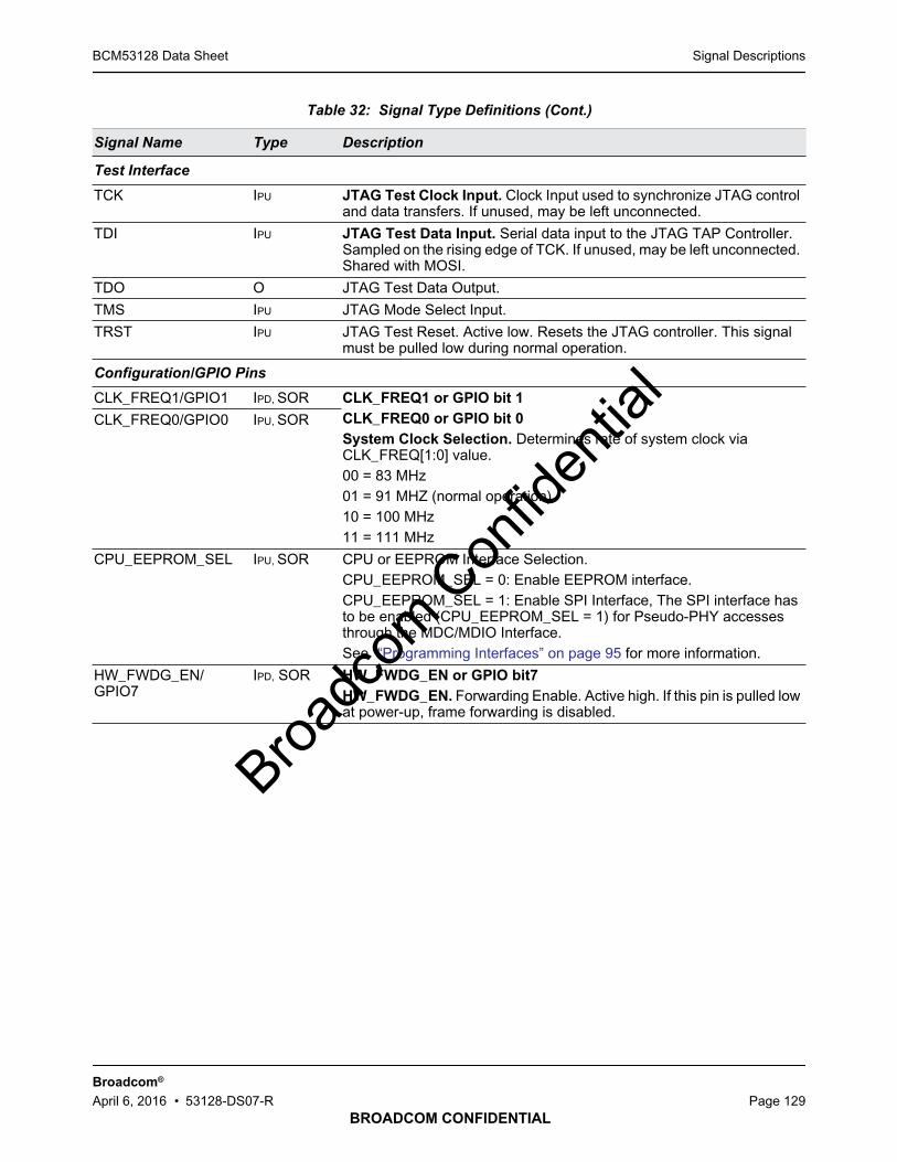
Signal DescriptionsBCM53128 Data Sheet
BROADCOM CONFIDENTIAL
Broadcom®
April 6, 2016 • 53128-DS07-R Page 129
Test Interface
TCK IPU JTAG Test Clock Input. Clock Input used to synchronize JTAG controland data transfers. If unused, may be left unconnected.
TDI IPU JTAG Test Data Input. Serial data input to the JTAG TAP Controller.Sampled on the rising edge of TCK. If unused, may be left unconnected.Shared with MOSI.
TDO O JTAG Test Data Output.
TMS IPU JTAG Mode Select Input.
TRST IPU JTAG Test Reset. Active low. Resets the JTAG controller. This signalmust be pulled low during normal operation.
Configuration/GPIO Pins
CLK_FREQ1/GPIO1 IPD, SOR CLK_FREQ1 or GPIO bit 1
CLK_FREQ0 or GPIO bit 0
System Clock Selection. Determines rate of system clock viaCLK_FREQ[1:0] value.00 = 83 MHz01 = 91 MHZ (normal operation)10 = 100 MHz11 = 111 MHz
CLK_FREQ0/GPIO0 IPU, SOR
CPU_EEPROM_SEL IPU, SOR CPU or EEPROM Interface Selection.CPU_EEPROM_SEL = 0: Enable EEPROM interface.CPU_EEPROM_SEL = 1: Enable SPI Interface, The SPI interface hasto be enabled (CPU_EEPROM_SEL = 1) for Pseudo-PHY accessesthrough the MDC/MDIO Interface.See ““Programming Interfaces” on page 95 for more information.
HW_FWDG_EN/GPIO7
IPD, SOR HW_FWDG_EN or GPIO bit7
HW_FWDG_EN. Forwarding Enable. Active high. If this pin is pulled lowat power-up, frame forwarding is disabled.
Table 32: Signal Type Definitions (Cont.)
Signal Name Type Description
Broadc
om C
onfid
entia
l

Signal DescriptionsBCM53128 Data Sheet
BROADCOM CONFIDENTIAL
Broadcom®
April 6, 2016 • 53128-DS07-R Page 130
LED MODE[1]/GPIO4LED MODE[0]/GPIO3
Bit 0: IPD,
Bit 1: IPU,
SOR
The following are LED Mode descriptions.LED Mode[1] or GPIO bit4, LED_MODE[0] or GPIO bit3
LED Mode. Users can select predefined functions to be displayed foreach port by setting the bits accordingly.When LED MODE[1:0] = 00
FE configurationSPD100MLNK/ACTPHYLED4
GbE configurationSPD1GSPD100MLNK/ACTPHYLED4
When LED MODE[1:0] = 01
FE configuration100M/ACT10M/ACTDPX/COLPHYLED4
GbE configuration1G/ACT10/100M/ACTDPX/COLPHYLED4
When LED MODE[1:0] = 10
FE configurationSPD100MLNK/ACTDPX
GbE configurationSPD1GSPD100MLNK/ACTDPX
Table 32: Signal Type Definitions (Cont.)
Signal Name Type Description
Broadc
om C
onfid
entia
l

Signal DescriptionsBCM53128 Data Sheet
BROADCOM CONFIDENTIAL
Broadcom®
April 6, 2016 • 53128-DS07-R Page 131
LED MODE[1]/GPIO4LED MODE[0]/GPIO3(continued fromprevious page)
When LED MODE[1:0] = 11
FE configuration100M/ACT10M/ACTDPX
GbE configuration1G/ACT100M/ACT10M/ACTDPX
IMP_SPD_SEL[1:0] Bit 0: IPD,
Bit 1: IPU
IMP Port Speed Select.
00 = 10 Mbps01 = 100 Mbps10 = 1000 Mbps (default)11 = 200 Mbps
IMP_MODE[1]/GPIO6IMP_MODE[0]/GPIO5
Bit 0: IPU,
Bit 1: IPU
SOR
IMP Mode[1] or GPIO bit6, IMP_MODE[0] or GPIO bit5
IMP Port Mode. Sets the mode of the IMP port based on the value ofthe pins IMP_MODE[1:0] at power-on reset.00 = RGMII mode01 = MII/TMII mode10 = RvMII/RvTMII mode11 = GMII mode
IMP_DUPLEX IPU IMP Port Duplex Mode.0 = IMP in half-duplex mode1 = IMP in full-duplex mode
IMP_LINK IPD IMP Port Link.0 = IMP link-down1 = IMP link-up
IMP_PAUSE_CAP_RX IPU Enable IMP Port Pause Capable in RX.
0 = Disable Pause capable1 = Enable Pause capable
IMP_PAUSE_CAP_TX IPU Enable IMP Port Pause Capable in TX.0 = Disable Pause capable1 = Enable Pause capable
IMP_VOL_SEL[1:0] IPD IMP Interface Voltage Control. RGMII needs to be set to 01 for 2.5V or1x for 1.5V. GMII/MII/TMII/RvMII/RvTMII needs to be set to 00 for 3.3V.00: 3.3V01: 2.5V10 or 11: 1.5V
Table 32: Signal Type Definitions (Cont.)
Signal Name Type Description
Broadc
om C
onfid
entia
l
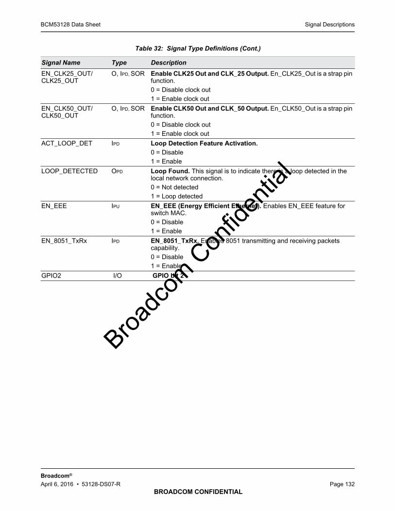
Signal DescriptionsBCM53128 Data Sheet
BROADCOM CONFIDENTIAL
Broadcom®
April 6, 2016 • 53128-DS07-R Page 132
EN_CLK25_OUT/CLK25_OUT
O, IPD, SOR Enable CLK25 Out and CLK_25 Output. En_CLK25_Out is a strap pinfunction.0 = Disable clock out1 = Enable clock out
EN_CLK50_OUT/CLK50_OUT
O, IPD, SOR Enable CLK50 Out and CLK_50 Output. En_CLK50_Out is a strap pinfunction.0 = Disable clock out1 = Enable clock out
ACT_LOOP_DET IPD Loop Detection Feature Activation.
0 = Disable1 = Enable
LOOP_DETECTED OPD Loop Found. This signal is to indicate there is a loop detected in thelocal network connection.0 = Not detected1 = Loop detected
EN_EEE IPU EN_EEE (Energy Efficient Ethernet). Enables EN_EEE feature forswitch MAC.0 = Disable1 = Enable
EN_8051_TxRx IPD EN_8051_TxRx. Enables 8051 transmitting and receiving packetscapability.0 = Disable1 = Enable
GPIO2 I/O GPIO bit 2
Table 32: Signal Type Definitions (Cont.)
Signal Name Type Description
Broadc
om C
onfid
entia
l

Signal DescriptionsBCM53128 Data Sheet
BROADCOM CONFIDENTIAL
Broadcom®
April 6, 2016 • 53128-DS07-R Page 133
LED Interface
LEDP0 O Port 7 Parallel LED Indicators. Active low.
LEDP1 O Port 7 Parallel LED Indicators. Active low.
LEDP2 O Port 7 Parallel LED Indicators. Active high.
LEDP3/En_Green O, IPD, SOR This is a dual function pin:Port 7 Parallel LED Indicators. Polarity determined at reset. See “DualInput Configuration/LED Output Function” on page 123.Green Mode Enable. Sampled on reset.1= Enable Green mode0= Disable Green mode
LEDP4 O Port 6 parallel LED Indicators. Active low.
LEDP5 O Port 6 parallel LED Indicators. Active low.
LEDP6 O Port 6 parallel LED Indicators. Active low.
LEDP7 O Port 6 parallel LED Indicators. Active high.
LEDP8 O Port 5 parallel LED Indicators. Active low.
LEDP9 O Port 5 parallel LED Indicators. Active low.
LEDP10/EEPROM_TYPE0
O, IPD, SOR This is a dual function pin.Port 5 Parallel LED Indicators. Polarity determined at reset. See “DualInput Configuration/LED Output Function” on page 123.Extended EEPROM Interface Selection. Sampled on reset.EEPROM_TYPE[1:0] = 00: Supports 93C46 EEPROMEEPROM_TYPE[1:0] = 01: Supports 93C56 EEPROMEEPROM_TYPE[1:0] = 10: Supports 93C66 EEPROMEEPROM_TYPE[1:0] = 11: Supports 93C86 EEPROM
LEDP11/EEPROM_TYPE1
O, IPD, SOR This is a dual function pin.Port 5 Parallel LED Indicators. Polarity determined at reset. See “DualInput Configuration/LED Output Function” on page 123.Extended EEPROM Interface Selection. Sampled on reset.EEPROM_TYPE [1:0] = 00: Supports 93C46 EEPROMEEPROM_TYPE [1:0] = 01: Supports 93C56 EEPROMEEPROM_TYPE [1:0] = 10: Supports 93C66 EEPROMEEPROM_TYPE [1:0] = 11: Supports 93C86 EEPROM
LEDP12 O Port 4 parallel LED Indicators. Active low.
LEDP13 O Port 4 parallel LED Indicators. Active low.
LEDP14/LOOP_DET_EN
O, IPD, SOR This is a dual function pin.Port 4 Parallel LED Indicators. Polarity determined at reset. See “DualInput Configuration/LED Output Function” on page 123.Enable Loop Detection Mode. Sampled on reset.0 = Disable1 = Enable
Table 32: Signal Type Definitions (Cont.)
Signal Name Type Description
Broadc
om C
onfid
entia
l

Signal DescriptionsBCM53128 Data Sheet
BROADCOM CONFIDENTIAL
Broadcom®
April 6, 2016 • 53128-DS07-R Page 134
LEDP15/LOOP_IMP_SEL
O, IPD, SOR This is a dual function pin.Port 4 Parallel LED Indicators. Polarity determined at reset. See “DualInput Configuration/LED Output Function” on page 123.Exclude IMP Port in Loop Detection Function. Sampled on reset.0 = Exclude IMP port from loop detection function1 = Include IMP port in loop detection function
LEDP16 O Port 3 Parallel LED Indicators. Active low.
LEDP17 O Port 3 Parallel LED Indicators. Active low.
LEDP18/BC_SUPP_EN
O, IPD, SOR This is a dual function pin.Port 3 Parallel LED Indicators. Polarity determined at reset. “DualInput Configuration/LED Output Function” on page 123.Broadcast Suppression Enable. Sampled on reset. See “RateControl” on page 45 for more information.0=Disable rate-based broadcast suppression.1=Enable rate-based broadcast suppression.
LEDP19 O Port 3 Parallel LED Indicators. Active high.
LEDP20 O Port 2 Parallel LED Indicators. Active low.
LEDP21 O Port 2 Parallel LED Indicators. Active low.
LEDP22/ DIS_IMP O, IPD, SOR This is a dual function pin.Port 2 Parallel LED Indicators. Polarity determined at reset. See “DualInput Configuration/LED Output Function” on page 123.Disables IMP Port. Sampled on reset.0 = Enable IMP port1 = Disable IMP port, and external pull-up resister is required.
LEDP23/IMP_DUMB_FWDG_EN
O, IPD, SOR This is a dual function pin.Port 2 Parallel LED Indicators. Polarity determined at reset. See “DualInput Configuration/LED Output Function” on page 123.IMP Port in Blocking State for Unmanaged Mode. Sampled on reset.When this pin is pulled up, the IMP port is not in management mode, theIMP port is in a regular port.0 = Blocking for dumb mode1 = Forwarding for dumb mode
LEDP24 O Port 1 Parallel LED Indicators. Active low.
LEDP25 O Port 1 Parallel LED Indicators. Active low.
LEDP26/ ENFDXFLOW O, IPU, SOR This is a dual function pin.Port 1 Parallel LED Indicators.
Polarity determined at reset. See “Dual Input Configuration/LED OutputFunction” on page 123.Enable Automatic Full-Duplex Flow Control. Sampled on reset.In combination with the results of auto-negotiation, sets the flow controlmode. See “Flow Control” on page 69 for more information.
Table 32: Signal Type Definitions (Cont.)
Signal Name Type Description
Broadc
om C
onfid
entia
l

Signal DescriptionsBCM53128 Data Sheet
BROADCOM CONFIDENTIAL
Broadcom®
April 6, 2016 • 53128-DS07-R Page 135
LEDP27/ENHDXFLOW
O, IPU, SOR This is a dual function pin.Port 1 Parallel LED Indicators.
Polarity determined at reset. See “Dual Input Configuration/LED OutputFunction” on page 123.Enable Automatic Backpressure. Sampled on reset.When this pin is pulled high, it enables half-duplex backpressure flowcontrol when a port is configured to half-duplex. See “Flow Control” onpage 69.
LEDP28 O Port 0 Parallel LED Indicators. Active low.
LEDP29 O Port 0 Parallel LED Indicators. Active low.
LEDP30/IMP_TXC_DELAY
O, IPD, SOR This is a dual function pin.Port 0 Parallel LED Indicators. Polarity determined at reset. See “DualInput Configuration/LED Output Function” on page 123.TXCLK Clock Timing Delay. Sampled on reset. Active high. This pinenables the TXCLK to data timing delay in RGMII mode. See “RGMIIInterface Timing” on page 304.
LEDP31/IMP_RXC_DELAY
O, IPD, SOR This is a dual function pin.Port 0 Parallel LED Indicators. Polarity determined at reset. See “DualInput Configuration/LED Output Function” on page 123.RXCLK Clock Timing Delay. Sampled on reset. Active high. This pinenables the RXCLK to data-sampling timing delay. See “RGMII InterfaceTiming” on page 304.
LEDCLK OPD LED Shift Clock. This clock is periodically active to enable LEDDATA toshift into external registers.
LEDDATA OPD Serial LED Data Output. Serial LED data for all ports is shifted out whenLEDCLK is active. LEDMODE[1:0] pins set the serial data content. See“LED Interface” on page 133 for a functional description of this signal.
Programming Interfaces
SCK IPD SPI Serial Clock. The clock input to the BCM53128 SPI interface issupplied by the SPI master, which supports up to 2 MHz, and is enabledif CPU_EPROM_SEL is high during power-on reset.
OPD EEPROM Serial Clock. The clock output to an external EEPROMdevice, and is enabled if CPU_EPROM_SEL is low during power-onreset. See the programming interfaces for more information.
SS/CS IPU SPI Slave Select. Active low signal which enables an SPI interface reador write operation. Enable if CPU_EPROM_SEL is high during power-onreset.
OPU EEPROM Chip Select. Active high control signal that enables a readoperation from an external EEPROM device. Enable ifCPU_EPROM_SEL is low during power-on reset. See the programminginterfaces for more information.
Table 32: Signal Type Definitions (Cont.)
Signal Name Type Description
Broadc
om C
onfid
entia
l
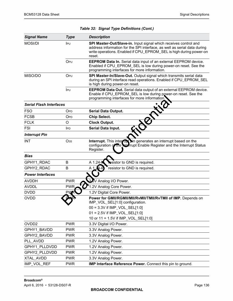
Signal DescriptionsBCM53128 Data Sheet
BROADCOM CONFIDENTIAL
Broadcom®
April 6, 2016 • 53128-DS07-R Page 136
MOSI/DI IPU SPI Master-Out/Slave-in. Input signal which receives control andaddress information for the SPI interface, as well as serial data duringwrite operations. Enabled if CPU_EPROM_SEL is high during power-onreset.
OPU EEPROM Data In. Serial data input of an external EEPROM device.Enabled if CPU_EPROM_SEL is low during power-on reset. See theprogramming interfaces for more information.
MISO/DO OPU SPI Master-In/Slave-Out. Output signal which transmits serial dataduring an SPI interface read operations. Enabled if CPU_EPROM_SELis high during power-on reset.
IPU EEPROM Data Out. Serial data output of an external EEPROM device.Enable if CPU_EPROM_SEL is low during power-on reset. See theprogramming interfaces for more information.
Serial Flash Interfaces
FSO OPD Serial Data Output.
FCSB OPD Chip Select.
FCLK O Clock Output.
FSI IPD Serial Data Input.
Interrupt Pin
INT O3S Interrupt. This interrupt pin generates an interrupt based on theconfiguration of the Interrupt Enable Register and the Interrupt StatusRegister.
Bias
GPHY1_RDAC B A 1.24-k resistor to GND is required.
GPHY2_RDAC B A 1.24-k resistor to GND is required.
Power Interfaces
AVDDH PWR 3.3V Analog I/O Power.
AVDDL PWR 1.2V Analog Core Power.
DVDD PWR 1.2V Digital Core Power.
OVDD PWR Power for GMII/RGMII/MII/RvMII/TMII/RvTMII of IMP. Depends onIMP_VOL_SEL[1:0] configuration.00 = 3.3V if IMP_VOL_SEL[1:0]01 = 2.5V if IMP_VOL_SEL[1:0]10 or 11 = 1.5V if IMP_VOL_SEL[1:0]
OVDD2 PWR 3.3V Digital I/O Power.
GPHY1_BAVDD PWR 3.3V Analog Power.
GPHY2_BAVDD PWR 3.3V Analog Power.
PLL_AVDD PWR 1.2V Analog Power.
GPHY1_PLLDVDD PWR 1.2V Analog Power.
GPHY2_PLLDVDD PWR 1.2V Analog Power.
XTAL_AVDD PWR 3.3V Analog Power.
IMP_VOL_REF PWR IMP Interface Reference Power. Connect this pin to ground.
Table 32: Signal Type Definitions (Cont.)
Signal Name Type Description
Broadc
om C
onfid
entia
l

Signal DescriptionsBCM53128 Data Sheet
BROADCOM CONFIDENTIAL
Broadcom®
April 6, 2016 • 53128-DS07-R Page 137
PLL_AVSS GND Shared Digital Ground.
XTAL_AVSS GND Shared Digital Ground.
EXPOSEPAD GND Ground.
No Connect
NC DNC Do not connect.
Table 32: Signal Type Definitions (Cont.)
Signal Name Type Description
Broadc
om C
onfid
entia
l

Pin AssignmentBCM53128 Data Sheet
BROADCOM CONFIDENTIAL
Broadcom®
April 6, 2016 • 53128-DS07-R Page 138
Section 6: Pin Assignment
BCM53128KQLE Pin List by Signal Name
Signal Ball
ACT_LOOP_DETECT
59
AVDDH 74
AVDDH 80
AVDDH 86
AVDDH 92
AVDDH 103
AVDDH 109
AVDDH 115
AVDDH 121
AVDDH 203
AVDDH 209
AVDDH 215
AVDDH 221
AVDDH 232
AVDDH 238
AVDDH 244
AVDDH 250
AVDDL 71
AVDDL 77
AVDDL 83
AVDDL 89
AVDDL 95
AVDDL 100
AVDDL 106
AVDDL 112
AVDDL 118
AVDDL 124
AVDDL 200
AVDDL 206
AVDDL 212
AVDDL 218
AVDDL 224
AVDDL 229
AVDDL 235
AVDDL 241
AVDDL 247
AVDDL 253
CLK_FREQ0/GPIO0 14
CLK_FREQ1/GPIO1 15
CPU_EEPROM_SEL 18
DVDD 16
DVDD 27
DVDD 31
DVDD 40
DVDD 53
DVDD 135
DVDD 148
DVDD 162
DVDD 169
DVDD 183
EN_8051_TxRx 47
EN_CLK25_OUT/CLK25_OUT
26
EN_CLK50_OUT/CLK50_OUT
21
EN_EEE 38
EXPOSEPAD H
FCSB 65
FSCLK 66
FSI 67
FSO 64
GPHY1_BVDD 227
GPHY1_PLLVDD 226
GPHY1_RDAC 228
GPHY2_BVDD 97
GPHY2_PLLVDD 98
GPHY2_RDAC 96
GPIO2 10
HW_FWDG_EN/GPIO7
9
IMP_COL 159
IMP_CRS 143
IMP_DUPLEX 52
IMP_GTXCLK 132
IMP_LINK 54
IMP_MODE0/GPIO5 7
IMP_MODE1/GPIO6 8
IMP_PAUSECAP_RX
55
Signal Ball
IMP_PAUSECAP_TX
56
IMP_RXCLK 144
IMP_RXD0 150
IMP_RXD1 151
IMP_RXD2 152
IMP_RXD3 154
IMP_RXD4 155
IMP_RXD5 156
IMP_RXD6 157
IMP_RXD7 158
IMP_RXDV 149
IMP_RXER 147
IMP_SPEED0 51
IMP_SPEED1 50
IMP_TXCLK 141
IMP_TXD0 137
IMP_TXD1 136
IMP_TXD2 134
IMP_TXD3 131
IMP_TXD4 130
IMP_TXD5 128
IMP_TXD6 127
IMP_TXD7 126
IMP_TXEN 139
IMP_TXER 140
IMP_VOL_REF 146
IMP_VOL_SEL0 49
IMP_VOL_SEL1 48
INTR_B 60
LEDCLK 167
LEDDATA 166
LEDMODE0/GPIO3 12
LEDMODE1/GPIO4 13
LEDP0 168
LEDP1 170
LEDP2 171
LEDP3/EN_GREEN 172
LEDP4 174
LEDP5 175
Signal Ball
LEDP6 176
LEDP7 177
LEDP8 178
LEDP9 179
LEDP10/EPROM_TYPE0
181
LEDP11/EPROM_TYPE1
182
LEDP12 184
LEDP13 185
LEDP14/LOOP_DETECT_EN
186
LEDP15/LOOP_IMP_SEL
188
LEDP16 189
LEDP17 190
LEDP18/BC_SUPP_EN
191
LEDP19 192
LEDP20 194
LEDP21 195
LEDP22/DIS_IMP 196
LEDP23/IMP_DUMB_FWDG_EN
197
LEDP24 198
LEDP25 199
LEDP26/ENFDXFLOW
254
LEDP27/ENHDXFLOW
255
LEDP28 256
LEDP29 1
LEDP30/IMP_TXC_DELAY
2
LEDP31/IMP_RXC_DELAY
4
LOOP_DETECTED 58
MDC 62
MDIO 61
MISO 161
MOSI 164
NC 5
Signal Ball
Broadc
om C
onfid
entia
l
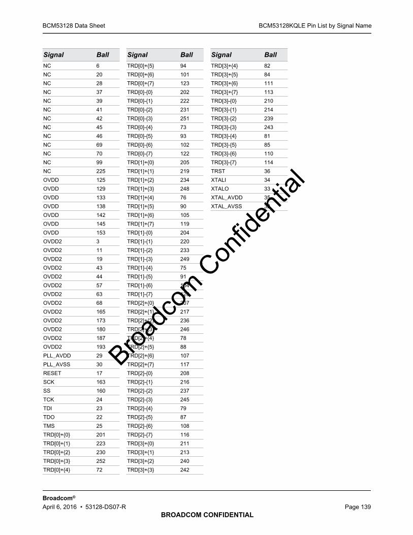
BCM53128KQLE Pin List by Signal NameBCM53128 Data Sheet
BROADCOM CONFIDENTIAL
Broadcom®
April 6, 2016 • 53128-DS07-R Page 139
NC 6
NC 20
NC 28
NC 37
NC 39
NC 41
NC 42
NC 45
NC 46
NC 69
NC 70
NC 99
NC 225
OVDD 125
OVDD 129
OVDD 133
OVDD 138
OVDD 142
OVDD 145
OVDD 153
OVDD2 3
OVDD2 11
OVDD2 19
OVDD2 43
OVDD2 44
OVDD2 57
OVDD2 63
OVDD2 68
OVDD2 165
OVDD2 173
OVDD2 180
OVDD2 187
OVDD2 193
PLL_AVDD 29
PLL_AVSS 30
RESET 17
SCK 163
SS 160
TCK 24
TDI 23
TDO 22
TMS 25
TRD[0]+{0} 201
TRD[0]+{1} 223
TRD[0]+{2} 230
TRD[0]+{3} 252
TRD[0]+{4} 72
Signal Ball
TRD[0]+{5} 94
TRD[0]+{6} 101
TRD[0]+{7} 123
TRD[0]-{0} 202
TRD[0]-{1} 222
TRD[0]-{2} 231
TRD[0]-{3} 251
TRD[0]-{4} 73
TRD[0]-{5} 93
TRD[0]-{6} 102
TRD[0]-{7} 122
TRD[1]+{0} 205
TRD[1]+{1} 219
TRD[1]+{2} 234
TRD[1]+{3} 248
TRD[1]+{4} 76
TRD[1]+{5} 90
TRD[1]+{6} 105
TRD[1]+{7} 119
TRD[1]-{0} 204
TRD[1]-{1} 220
TRD[1]-{2} 233
TRD[1]-{3} 249
TRD[1]-{4} 75
TRD[1]-{5} 91
TRD[1]-{6} 104
TRD[1]-{7} 120
TRD[2]+{0} 207
TRD[2]+{1} 217
TRD[2]+{2} 236
TRD[2]+{3} 246
TRD[2]+{4} 78
TRD[2]+{5} 88
TRD[2]+{6} 107
TRD[2]+{7} 117
TRD[2]-{0} 208
TRD[2]-{1} 216
TRD[2]-{2} 237
TRD[2]-{3} 245
TRD[2]-{4} 79
TRD[2]-{5} 87
TRD[2]-{6} 108
TRD[2]-{7} 116
TRD[3]+{0} 211
TRD[3]+{1} 213
TRD[3]+{2} 240
TRD[3]+{3} 242
Signal Ball
TRD[3]+{4} 82
TRD[3]+{5} 84
TRD[3]+{6} 111
TRD[3]+{7} 113
TRD[3]-{0} 210
TRD[3]-{1} 214
TRD[3]-{2} 239
TRD[3]-{3} 243
TRD[3]-{4} 81
TRD[3]-{5} 85
TRD[3]-{6} 110
TRD[3]-{7} 114
TRST 36
XTALI 34
XTALO 33
XTAL_AVDD 35
XTAL_AVSS 32
Signal Ball
Broadc
om C
onfid
entia
l

BCM53128KQLE Pin List by Ball NumberBCM53128 Data Sheet
BROADCOM CONFIDENTIAL
Broadcom®
April 6, 2016 • 53128-DS07-R Page 140
BCM53128KQLE Pin List by Ball Number
Ball Signal
1 LEDP29
2 LEDP30/IMP_TXC_DELAY
3 OVDD2
4 LEDP31/IMP_RXC_DELAY
5 NC
6 NC
7 IMP_MODE0/GPIO5
8 IMP_MODE1/GPIO6
9 HW_FWDG_EN/GPIO7
10 GPIO2
11 OVDD2
12 LEDMODE0/GPIO3
13 LEDMODE1/GPIO4
14 CLK_FREQ0/GPIO0
15 CLK_FREQ1/GPIO1
16 DVDD
17 RESET
18 CPU_EEPROM_SEL
19 OVDD2
20 NC
21 EN_CLK50_OUT/CLK50_OUT
22 TDO
23 TDI
24 TCK
25 TMS
26 EN_CLK25_OUT/CLK25_OUT
27 DVDD
28 NC
29 PLL_AVDD
30 PLL_AVSS
31 DVDD
32 XTAL_AVSS
33 XTALO
34 XTALI
35 XTAL_AVDD
36 TRST
37 NC
38 EN_EEE
39 NC
40 DVDD
41 NC
42 NC
43 OVDD2
44 OVDD2
45 NC
46 NC
47 EN_8051_TxRx
48 IMP_VOL_SEL1
49 IMP_VOL_SEL0
50 IMP_SPEED1
51 IMP_SPEED0
52 IMP_DUPLEX
53 DVDD
54 IMP_LINK
55 IMP_PAUSECAP_RX
56 IMP_PAUSECAP_TX
57 OVDD2
58 LOOP_DETECTED
59 ACT_LOOP_DETECT
60 INTR_B
61 MDIO
62 MDC
63 OVDD2
64 FSO
65 FCSB
66 FSCLK
67 FSI
68 OVDD2
69 NC
70 NC
71 AVDDL
72 TRD[0]+{4}
73 TRD[0]-{4}
74 AVDDH
75 TRD[1]-{4}
76 TRD[1]+{4}
77 AVDDL
78 TRD[2]+{4}
79 TRD[2]-{4}
80 AVDDH
81 TRD[3]-{4}
82 TRD[3]+{4}
Ball Signal
83 AVDDL
84 TRD[3]+{5}
85 TRD[3]-{5}
86 AVDDH
87 TRD[2]-{5}
88 TRD[2]+{5}
89 AVDDL
90 TRD[1]+{5}
91 TRD[1]-{5}
92 AVDDH
93 TRD[0]-{5}
94 TRD[0]+{5}
95 AVDDL
96 GPHY2_RDAC
97 GPHY2_BVDD
98 GPHY2_PLLVDD
99 NC
100 AVDDL
101 TRD[0]+{6}
102 TRD[0]-{6}
103 AVDDH
104 TRD[1]-{6}
105 TRD[1]+{6}
106 AVDDL
107 TRD[2]+{6}
108 TRD[2]-{6}
109 AVDDH
110 TRD[3]-{6}
111 TRD[3]+{6}
112 AVDDL
113 TRD[3]+{7}
114 TRD[3]-{7}
115 AVDDH
116 TRD[2]-{7}
117 TRD[2]+{7}
118 AVDDL
119 TRD[1]+{7}
120 TRD[1]-{7}
121 AVDDH
122 TRD[0]-{7}
123 TRD[0]+{7}
124 AVDDL
125 OVDD
126 IMP_TXD7
Ball Signal
127 IMP_TXD6
128 IMP_TXD5
129 OVDD
130 IMP_TXD4
131 IMP_TXD3
132 IMP_GTXCLK
133 OVDD
134 IMP_TXD2
135 DVDD
136 IMP_TXD1
137 IMP_TXD0
138 OVDD
139 IMP_TXEN
140 IMP_TXER
141 IMP_TXCLK
142 OVDD
143 IMP_CRS
144 IMP_RXCLK
145 OVDD
146 IMP_VOL_REF
147 IMP_RXER
148 DVDD
149 IMP_RXDV
150 IMP_RXD0
151 IMP_RXD1
152 IMP_RXD2
153 OVDD
154 IMP_RXD3
155 IMP_RXD4
156 IMP_RXD5
157 IMP_RXD6
158 IMP_RXD7
159 IMP_COL
160 SS
161 MISO
162 DVDD
163 SCK
164 MOSI
165 OVDD2
166 LEDDATA
167 LEDCLK
168 LEDP0
169 DVDD
170 LEDP1
Ball Signal
Broadc
om C
onfid
entia
l

BCM53128KQLE Pin List by Ball NumberBCM53128 Data Sheet
BROADCOM CONFIDENTIAL
Broadcom®
April 6, 2016 • 53128-DS07-R Page 141
171 LEDP2
172 LEDP3/EN_GREEN
173 OVDD2
174 LEDP4
175 LEDP5
176 LEDP6
177 LEDP7
178 LEDP8
179 LEDP9
180 OVDD2
181 LEDP10/EPROM_TYPE0
182 LEDP11/EPROM_TYPE1
183 DVDD
184 LEDP12
185 LEDP13
186 LEDP14/LOOP_DETECT_EN
187 OVDD2
188 LEDP15/LOOP_IMP_SEL
189 LEDP16
190 LEDP17
191 LEDP18/BC_SUPP_EN
192 LEDP19
193 OVDD2
194 LEDP20
195 LEDP21
196 LEDP22/DIS_IMP
197 LEDP23/IMP_DUMB_FWDG_EN
198 LEDP24
199 LEDP25
200 AVDDL
201 TRD[0]+{0}
202 TRD[0]-{0}
203 AVDDH
204 TRD[1]-{0}
205 TRD[1]+{0}
206 AVDDL
207 TRD[2]+{0}
208 TRD[2]-{0}
209 AVDDH
210 TRD[3]-{0}
211 TRD[3]+{0}
212 AVDDL
Ball Signal
213 TRD[3]+{1}
214 TRD[3]-{1}
215 AVDDH
216 TRD[2]-{1}
217 TRD[2]+{1}
218 AVDDL
219 TRD[1]+{1}
220 TRD[1]-{1}
221 AVDDH
222 TRD[0]-{1}
223 TRD[0]+{1}
224 AVDDL
225 NC
226 GPHY1_PLLVDD
227 GPHY1_BVDD
228 GPHY1_RDAC
229 AVDDL
230 TRD[0]+{2}
231 TRD[0]-{2}
232 AVDDH
233 TRD[1]-{2}
234 TRD[1]+{2}
235 AVDDL
236 TRD[2]+{2}
237 TRD[2]-{2}
238 AVDDH
239 TRD[3]-{2}
240 TRD[3]+{2}
241 AVDDL
242 TRD[3]+{3}
243 TRD[3]-{3}
244 AVDDH
245 TRD[2]-{3}
246 TRD[2]+{3}
247 AVDDL
248 TRD[1]+{3}
249 TRD[1]-{3}
250 AVDDH
251 TRD[0]-{3}
252 TRD[0]+{3}
253 AVDDL
254 LEDP26/ENFDXFLOW
255 LEDP27/ENHDXFLOW
256 LEDP28
H EXPOSEPAD
Ball Signal
Broadc
om C
onfid
entia
l

Register DefinitionsBCM53128 Data Sheet
BROADCOM CONFIDENTIAL
Broadcom®
April 6, 2016 • 53128-DS07-R Page 142
Section 7: Register Definit ions
Register Definition
BCM53128 register sets can be accessed through the programming interfaces described on page 95. Theregister space is organized into pages, each containing a certain set of registers. Table 33 lists the pagesdefined in the BCM53128. To access a page, the page register (0xFF) is written with the page value. Theregisters contained in the page can then be accessed by their addresses. See “Programming Interfaces” onpage 95 for more information.
Register Notations
In the register description tables, the following notation in the R/W column is used to describe the ability to reador to write:
• R/W = Read or write
• RO = Read only
• LH = Latched high
• LL = Latched low
• H = Fixed high
• L = Fixed low
• SC = Clear on read
Reserved bits must be written as the default value and ignored when read.
Global Page Register
Table 33: Global Page Register Map
Page Description
00h “Page 00h: Control Registers” on page 144
01h “Page 01h: Status Registers” on page 164
02h “Page 02h: Management/Mirroring Registers” on page 168
03h “Page 03h: Interrupt Control Register” on page 177
04h “Page 03h: Interrupt Control Register” on page 177
05h “Page 05h: ARL/VTBL Access Registers” on page 184
06h, 07h Reserved
08h Reserved
09h Reserved
Broadc
om C
onfid
entia
l
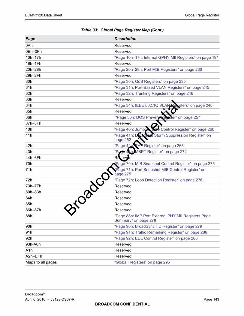
Global Page RegisterBCM53128 Data Sheet
BROADCOM CONFIDENTIAL
Broadcom®
April 6, 2016 • 53128-DS07-R Page 143
0Ah Reserved
0Bh–0Fh Reserved
10h–17h “Page 10h–17h: Internal GPHY MII Registers” on page 194
18h–1Fh Reserved
20h–28h “Page 20h–28h: Port MIB Registers” on page 230
29h–2Fh Reserved
30h “Page 30h: QoS Registers” on page 235
31h “Page 31h: Port-Based VLAN Registers” on page 245
32h “Page 32h: Trunking Registers” on page 246
33h Reserved
34h “Page 34h: IEEE 802.1Q VLAN Registers” on page 248
35h Reserved
36h “Page 36h: DOS Prevent Register” on page 257
37h–3Fh Reserved
40h “Page 40h: Jumbo Frame Control Register” on page 260
41h “Page 41h: Broadcast Storm Suppression Register” onpage 262
42h “Page 42h: EAP Register” on page 268
43h “Page 43h: MSPT Register” on page 272
44h–6Fh Reserved
70h “Page 70h: MIB Snapshot Control Register” on page 275
71h “Page 71h: Port Snapshot MIB Control Register” onpage 275
72h “Page 72h: Loop Detection Register” on page 276
73h–7Fh Reserved
80h–83h Reserved
84h Reserved
85h Reserved
86h–87h Reserved
88h “Page 88h: IMP Port External PHY MII Registers PageSummary” on page 278
90h “Page 90h: BroadSync HD Register” on page 279
91h “Page 91h: Traffic Remarking Register” on page 286
92h “Page 92h: EEE Control Register” on page 288
93h-A0h Reserved
A1h Reserved
A2h–EFh Reserved
Maps to all pages “Global Registers” on page 295
Table 33: Global Page Register Map (Cont.)
Page Description
Broadc
om C
onfid
entia
l
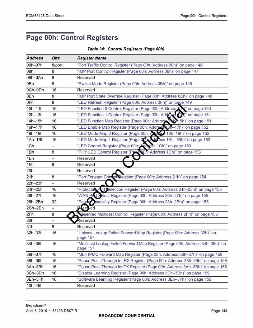
Page 00h: Control RegistersBCM53128 Data Sheet
BROADCOM CONFIDENTIAL
Broadcom®
April 6, 2016 • 53128-DS07-R Page 144
Page 00h: Control Registers
Table 34: Control Registers (Page 00h)
Address Bits Register Name
00h–07h 8/port “Port Traffic Control Register (Page 00h: Address 00h)” on page 146
08h 8 “IMP Port Control Register (Page 00h: Address 08h)” on page 147
09h–0Ah 8 Reserved
0Bh 8 “Switch Mode Register (Page 00h: Address 0Bh)” on page 148
0Ch–0Dh 16 Reserved
0Eh 8 “IMP Port State Override Register (Page 00h: Address 0Eh)” on page 148
0Fh 8 “LED Refresh Register (Page 00h: Address 0Fh)” on page 149
10h–11h 16 “LED Function 0 Control Register (Page 00h: Address 10h)” on page 150
12h–13h 16 “LED Function 1 Control Register (Page 00h: Address 12h)” on page 151
14h–15h 16 “LED Function Map Register (Page 00h: Address 14h–15h)” on page 151
16h–17h 16 “LED Enable Map Register (Page 00h: Address 16h–17h)” on page 152
18h–19h 16 “LED Mode Map 0 Register (Page 00h: Address 18h–19h)” on page 152
1Ah–1Bh 16 “LED Mode Map 1 Register (Page 00h: Address 1Ah–1Bh)” on page 152
1Ch – “LED Control Register (Page 00h: Address 1Ch)” on page 153
1Dh 8 “PHY LED Control Register (Page 00h: Address 1Dh)” on page 153
1Eh – Reserved
1Fh 8 Reserved
20h – Reserved
21h 8 “Port Forward Control Register (Page 00h: Address 21h)” on page 154
22h–23h – Reserved
24h–25h 16 “Protected Port Selection Register (Page 00h: Address 24h–25h)” on page 155
26h–27h 16 “WAN Port Select Register (Page 00h: Address 26h–27h)” on page 155
28h–2Bh 32 “Pause Capability Register (Page 00h: Address 28h–2Bh)” on page 155
2Ch–2Eh – Reserved
2Fh 8 “Reserved Multicast Control Register (Page 00h: Address 2Fh)” on page 156
30h – Reserved
31h 8 Reserved
32h–33h 16 “Unicast Lookup Failed Forward Map Register (Page 00h: Address 32h)” onpage 157
34h–35h 16 “Multicast Lookup Failed Forward Map Register (Page 00h: Address 34h–35h)” onpage 157
36h–37h 16 “MLF IPMC Forward Map Register (Page 00h: Address 36h–37h)” on page 158
38h–39h 16 “Pause Pass Through for RX Register (Page 00h: Address 38h–39h)” on page 158
3Ah–3Bh 16 “Pause Pass Through for TX Register (Page 00h: Address 3Ah–3Bh)” on page 158
3Ch–3Dh 16 “Disable Learning Register (Page 00h: Address 3Ch–3Dh)” on page 159
3Eh–3Fh 16 “Software Learning Register (Page 00h: Address 3Eh–3Fh)” on page 159
40h–49h – Reserved
Broadc
om C
onfid
entia
l
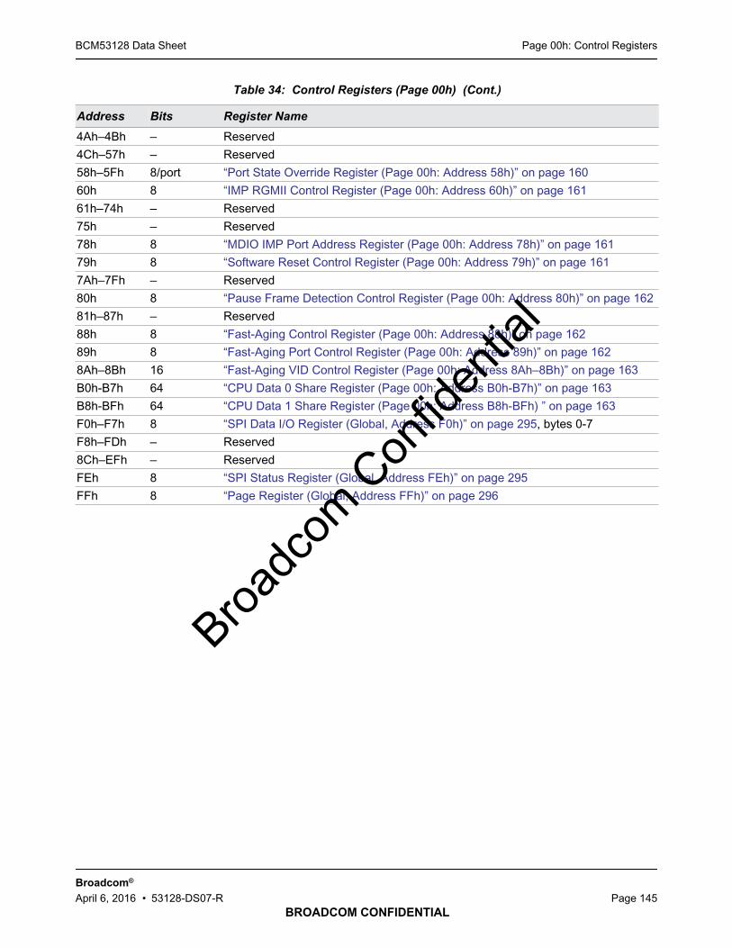
Page 00h: Control RegistersBCM53128 Data Sheet
BROADCOM CONFIDENTIAL
Broadcom®
April 6, 2016 • 53128-DS07-R Page 145
4Ah–4Bh – Reserved
4Ch–57h – Reserved
58h–5Fh 8/port “Port State Override Register (Page 00h: Address 58h)” on page 160
60h 8 “IMP RGMII Control Register (Page 00h: Address 60h)” on page 161
61h–74h – Reserved
75h – Reserved
78h 8 “MDIO IMP Port Address Register (Page 00h: Address 78h)” on page 161
79h 8 “Software Reset Control Register (Page 00h: Address 79h)” on page 161
7Ah–7Fh – Reserved
80h 8 “Pause Frame Detection Control Register (Page 00h: Address 80h)” on page 162
81h–87h – Reserved
88h 8 “Fast-Aging Control Register (Page 00h: Address 88h)” on page 162
89h 8 “Fast-Aging Port Control Register (Page 00h: Address 89h)” on page 162
8Ah–8Bh 16 “Fast-Aging VID Control Register (Page 00h: Address 8Ah–8Bh)” on page 163
B0h-B7h 64 “CPU Data 0 Share Register (Page 00h: Address B0h-B7h)” on page 163
B8h-BFh 64 “CPU Data 1 Share Register (Page 00h: Address B8h-BFh) ” on page 163
F0h–F7h 8 “SPI Data I/O Register (Global, Address F0h)” on page 295, bytes 0-7
F8h–FDh – Reserved
8Ch–EFh – Reserved
FEh 8 “SPI Status Register (Global, Address FEh)” on page 295
FFh 8 “Page Register (Global, Address FFh)” on page 296
Table 34: Control Registers (Page 00h) (Cont.)
Address Bits Register Name
Broadc
om C
onfid
entia
l

Page 00h: Control RegistersBCM53128 Data Sheet
BROADCOM CONFIDENTIAL
Broadcom®
April 6, 2016 • 53128-DS07-R Page 146
Port Traffic Control Register (Page 00h: Address 00h).
Table 35: Port Traffic Control Register Address Summary
Address Description
00h Port 0
01h Port 1
02h Port 2
03h Port 3
04h Port 4
05h Port 5
06h Port 6
07h Port 7
Table 36: Port Control Register (Page 00h: Address 00h–07h)
BIt Name R/W Description Default
7:5 STP_STATE[2:0] R/W CPU writes the current computed states of itsspanning tree algorithm for a given port.000 = No spanning tree (default for unmanagedmode)001 = Disabled state (default for managed mode)010 = Blocking state011 = Listening state100 = Learning state101 = Forwarding state110–111 = Reserved
~ HW_FWDG_EN
4:2 Reserved – – 000
1 TX_DISABLE R/W 0 = Enable the transmit function of the port at the MAClevel.1 = Disable the transmit function of the port at theMAC level.
0
0 RX_DISABLE R/W 0 = Enable the receive function of the port at the MAClevel.1 = Disable the receive function of the port at the MAClevel.
0Broadc
om C
onfid
entia
l
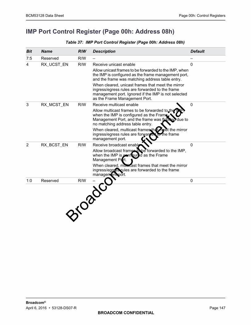
Page 00h: Control RegistersBCM53128 Data Sheet
BROADCOM CONFIDENTIAL
Broadcom®
April 6, 2016 • 53128-DS07-R Page 147
IMP Port Control Register (Page 00h: Address 08h)
Table 37: IMP Port Control Register (Page 00h: Address 08h)
Bit Name R/W Description Default
7:5 Reserved R/W – –
4 RX_UCST_EN R/W Receive unicast enableAllow unicast frames to be forwarded to the IMP, whenthe IMP is configured as the frame management port,and the frame was matching address table entry.When cleared, unicast frames that meet the mirroringress/egress rules are forwarded to the framemanagement port. Ignored if the IMP is not selectedas the Frame Management Port.
0
3 RX_MCST_EN R/W Receive multicast enableAllow multicast frames to be forwarded to the IMP,when the IMP is configured as the FrameManagement Port, and the frame was flooded due tono matching address table entry.When cleared, multicast frames that meet the mirroringress/egress rules are forwarded to the framemanagement port.
0
2 RX_BCST_EN R/W Receive broadcast enableAllow broadcast frames to be forwarded to the IMP,when the IMP is configured as the FrameManagement Port.When cleared, multicast frames that meet the mirroringress/egress rules are forwarded to the framemanagement port.
0
1:0 Reserved R/W – 0
Broadc
om C
onfid
entia
l
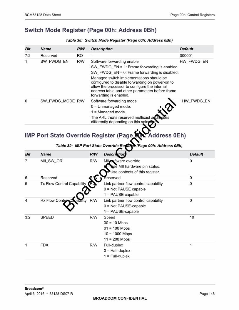
Page 00h: Control RegistersBCM53128 Data Sheet
BROADCOM CONFIDENTIAL
Broadcom®
April 6, 2016 • 53128-DS07-R Page 148
Switch Mode Register (Page 00h: Address 0Bh)
IMP Port State Override Register (Page 00h: Address 0Eh)
Table 38: Switch Mode Register (Page 00h: Address 0Bh)
Bit Name R/W Description Default
7:2 Reserved RO – 000001
1 SW_FWDG_EN R/W Software forwarding enableSW_FWDG_EN = 1: Frame forwarding is enabled.SW_FWDG_EN = 0: Frame forwarding is disabled.Managed switch implementations should beconfigured to disable forwarding on power-on toallow the processor to configure the internaladdress table and other parameters before frameforwarding is enabled.
HW_FWDG_EN
0 SW_FWDG_MODE R/W Software forwarding mode0 = Unmanaged mode.1 = Managed mode.The ARL treats reserved multicast addressesdifferently depending on this selection.
~HW_FWDG_EN
Table 39: IMP Port State Override Register (Page 00h: Address 0Eh)
Bit Name R/W Description Default
7 MII_SW_OR R/W MII software override0 = Use MII hardware pin status.1 = Use contents of this register.
0
6 Reserved R/W Reserved 0
5 Tx Flow Control Capability RO Link partner flow control capability0 = Not PAUSE capable1 = PAUSE capable
0
4 Rx Flow Control Capability R/W Link partner flow control capability0 = Not PAUSE-capable1 = PAUSE-capable
0
3:2 SPEED R/W Speed00 = 10 Mbps01 = 100 Mbps10 = 1000 Mbps11 = 200 Mbps
10
1 FDX R/W Full-duplex0 = Half-duplex1 = Full-duplex
1
Broadc
om C
onfid
entia
l
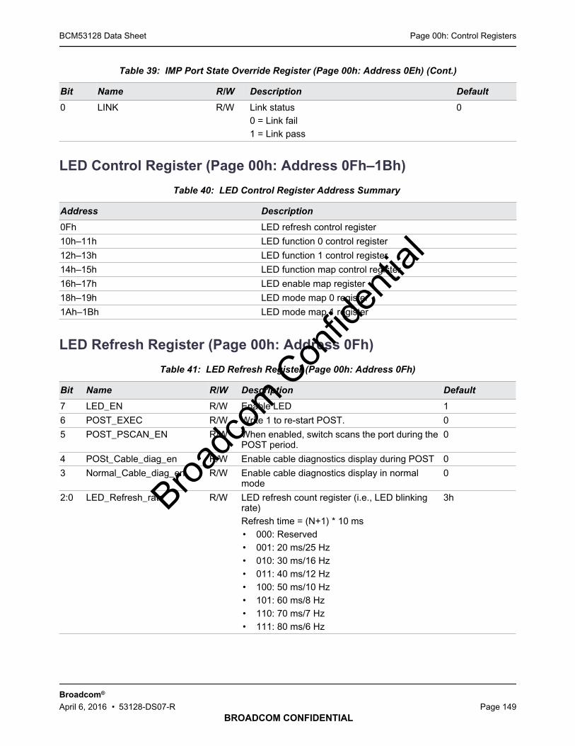
Page 00h: Control RegistersBCM53128 Data Sheet
BROADCOM CONFIDENTIAL
Broadcom®
April 6, 2016 • 53128-DS07-R Page 149
LED Control Register (Page 00h: Address 0Fh–1Bh)
LED Refresh Register (Page 00h: Address 0Fh)
0 LINK R/W Link status0 = Link fail1 = Link pass
0
Table 40: LED Control Register Address Summary
Address Description
0Fh LED refresh control register
10h–11h LED function 0 control register
12h–13h LED function 1 control register
14h–15h LED function map control register
16h–17h LED enable map register
18h–19h LED mode map 0 register
1Ah–1Bh LED mode map 1 register
Table 41: LED Refresh Register (Page 00h: Address 0Fh)
Bit Name R/W Description Default
7 LED_EN R/W Enable LED 1
6 POST_EXEC R/W Write 1 to re-start POST. 0
5 POST_PSCAN_EN R/W When enabled, switch scans the port during thePOST period.
0
4 POSt_Cable_diag_en R/W Enable cable diagnostics display during POST 0
3 Normal_Cable_diag_en R/W Enable cable diagnostics display in normalmode
0
2:0 LED_Refresh_rate R/W LED refresh count register (i.e., LED blinkingrate)Refresh time = (N+1) * 10 ms• 000: Reserved• 001: 20 ms/25 Hz• 010: 30 ms/16 Hz• 011: 40 ms/12 Hz• 100: 50 ms/10 Hz• 101: 60 ms/8 Hz• 110: 70 ms/7 Hz• 111: 80 ms/6 Hz
3h
Table 39: IMP Port State Override Register (Page 00h: Address 0Eh) (Cont.)
Bit Name R/W Description Default
Broadc
om C
onfid
entia
l

Page 00h: Control RegistersBCM53128 Data Sheet
BROADCOM CONFIDENTIAL
Broadcom®
April 6, 2016 • 53128-DS07-R Page 150
LED Function 0 Control Register (Page 00h: Address 10h)
Table 42: LED Function 0 Control Register (Page 00h: Address 10h–11h)
Bit Name R/W Description Default
15:0 LED_FUNCTION R/W The following is the list of functions assignedto each bit:15: Reserved14: BroadSync HD Link13: 1G/ACT12: 10/100M/ACT11: 100M/ACT10: 10M/ACT9: SPD1G8: SPD100M7: SPD10M6: DPX/COL5: LNK/ACT4: COL3: ACT2: DPX1: LNK0: Reserved
LED MODE[1:0] = 00:16'h0120LED MODE[1:0] = 01:16'h0C40LED MODE[1:0] = 10:16'h0124LED MODE[1:0] = 11:16'h0C04
Broadc
om C
onfid
entia
l
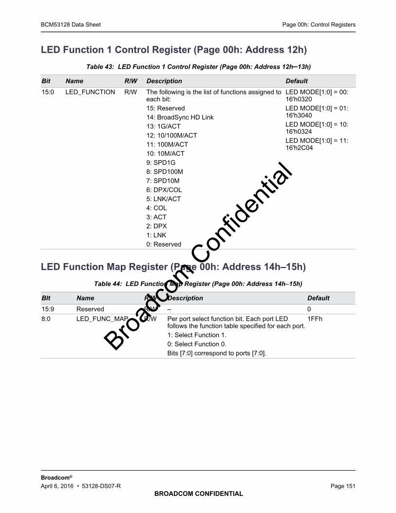
Page 00h: Control RegistersBCM53128 Data Sheet
BROADCOM CONFIDENTIAL
Broadcom®
April 6, 2016 • 53128-DS07-R Page 151
LED Function 1 Control Register (Page 00h: Address 12h)
LED Function Map Register (Page 00h: Address 14h–15h)
Table 43: LED Function 1 Control Register (Page 00h: Address 12h–13h)
Bit Name R/W Description Default
15:0 LED_FUNCTION R/W The following is the list of functions assigned toeach bit:15: Reserved14: BroadSync HD Link13: 1G/ACT12: 10/100M/ACT11: 100M/ACT10: 10M/ACT9: SPD1G8: SPD100M7: SPD10M6: DPX/COL5: LNK/ACT4: COL3: ACT2: DPX1: LNK0: Reserved
LED MODE[1:0] = 00:16'h0320LED MODE[1:0] = 01:16'h3040LED MODE[1:0] = 10:16'h0324LED MODE[1:0] = 11:16'h2C04
Table 44: LED Function Map Register (Page 00h: Address 14h–15h)
BIt Name R/W Description Default
15:9 Reserved R/W – 0
8:0 LED_FUNC_MAP R/W Per port select function bit. Each port LEDfollows the function table specified for each port.1: Select Function 1.0: Select Function 0.Bits [7:0] correspond to ports [7:0].
1FFh
Broadc
om C
onfid
entia
l
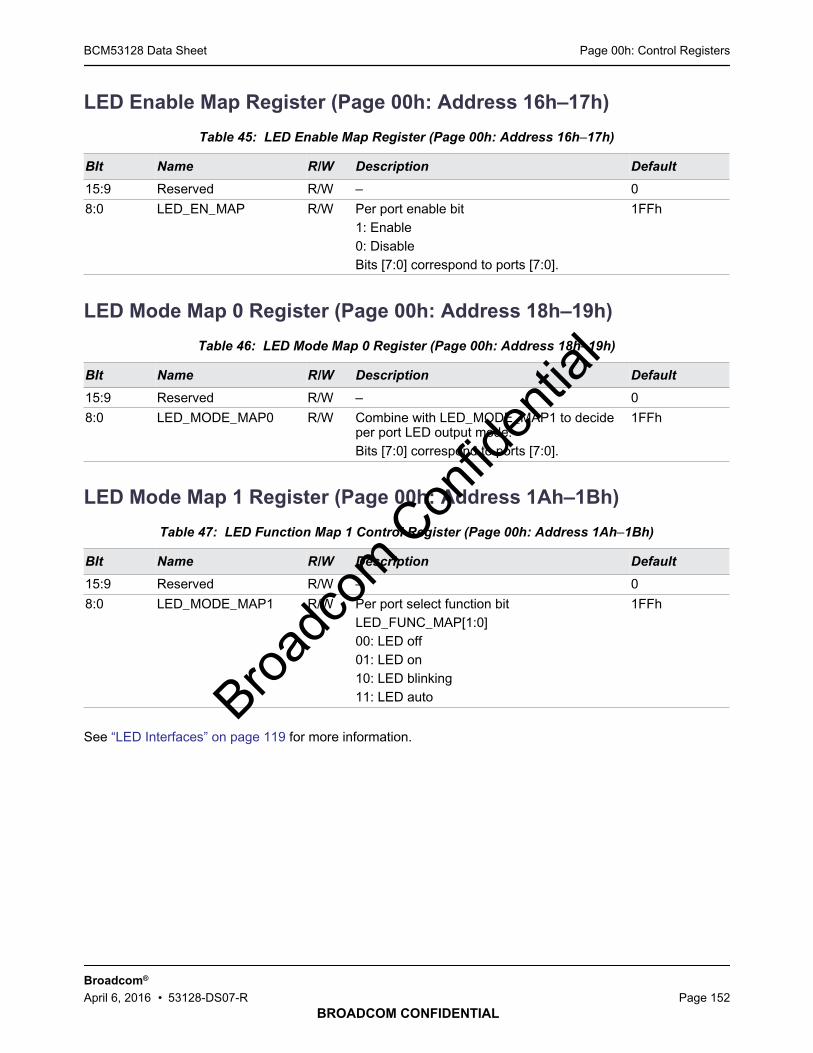
Page 00h: Control RegistersBCM53128 Data Sheet
BROADCOM CONFIDENTIAL
Broadcom®
April 6, 2016 • 53128-DS07-R Page 152
LED Enable Map Register (Page 00h: Address 16h–17h)
LED Mode Map 0 Register (Page 00h: Address 18h–19h)
LED Mode Map 1 Register (Page 00h: Address 1Ah–1Bh)
See “LED Interfaces” on page 119 for more information.
Table 45: LED Enable Map Register (Page 00h: Address 16h–17h)
BIt Name R/W Description Default
15:9 Reserved R/W – 0
8:0 LED_EN_MAP R/W Per port enable bit1: Enable0: DisableBits [7:0] correspond to ports [7:0].
1FFh
Table 46: LED Mode Map 0 Register (Page 00h: Address 18h–19h)
BIt Name R/W Description Default
15:9 Reserved R/W – 0
8:0 LED_MODE_MAP0 R/W Combine with LED_MODE_MAP1 to decideper port LED output mode.Bits [7:0] correspond to ports [7:0].
1FFh
Table 47: LED Function Map 1 Control Register (Page 00h: Address 1Ah–1Bh)
BIt Name R/W Description Default
15:9 Reserved R/W – 0
8:0 LED_MODE_MAP1 R/W Per port select function bitLED_FUNC_MAP[1:0]00: LED off01: LED on10: LED blinking11: LED auto
1FFh
Broadc
om C
onfid
entia
l

Page 00h: Control RegistersBCM53128 Data Sheet
BROADCOM CONFIDENTIAL
Broadcom®
April 6, 2016 • 53128-DS07-R Page 153
LED Control Register (Page 00h: Address 1Ch)
PHY LED Control Register (Page 00h: Address 1Dh)
Table 48: LED Control Register (Page 00h: Address 1Ch)
BIt Name R/W Description Default
7:4 POST_LED_CTRL R/W Post LED ControlThe four bits control the LED ON/OFF state during POST toallow dual-color LED to be tested.Bits[7:4] control each port four LED pins as below.Port 0 LEDP[31:28]Port 1 LEDP[27:24]Port 2 LEDP[23:20]Port 3 LEDP[19:16]Port 4 LEDP[15:12]Port 5 LEDP[11:8]Port 6 LEDP[7:4]Port 7 LEDP[3:0]1: The LED pin is activated during POST.0: The LED pin is deactivated during POST.
0xF
3 DUAL_LED_CTRL R/W Dual-color LED Test Control1: One side of the dual-color LED, which correspondingPOST_LED_CTRL bit = 1, will be tested during POST firstly,and then test the other side of the dual-color LED, whichcorresponding POST_LED_CTRL bit = 0.0: Only one side of the dual-color LED, which correspondingPOST_LED_CTRL bit = 1, will be tested during POST.
0x0
2:0 Reserved R/W Reserved 0x0
Table 49: PHY LED Control Register (Page 00h: Address 1Dh)
BIt Name R/W Description Default
7:4 PHY_LED_FUNC1 R/W Bit 7: PHYLED4 of LED Function 1Bit 6: PHYLED3 of LED Function 1Bit 5: PHYLED2 of LED Function 1Bit 4: PHYLED1 of LED Function 1
LED Mode[1:0] = 00: 8'h88LED Mode[1:0] = 01: 8'h88
3:0 PHY_LED_FUNC0 R/W Bit 3: PHYLED4 of LED Function 0Bit 2: PHYLED3 of LED Function 0Bit 1: PHYLED2 of LED Function 0Bit 0: PHYLED1 of LED Function 0
LED Mode[1:0] = 10: 8''h00LED Mode[1:0] = 11: 8'h00
Broadc
om C
onfid
entia
l
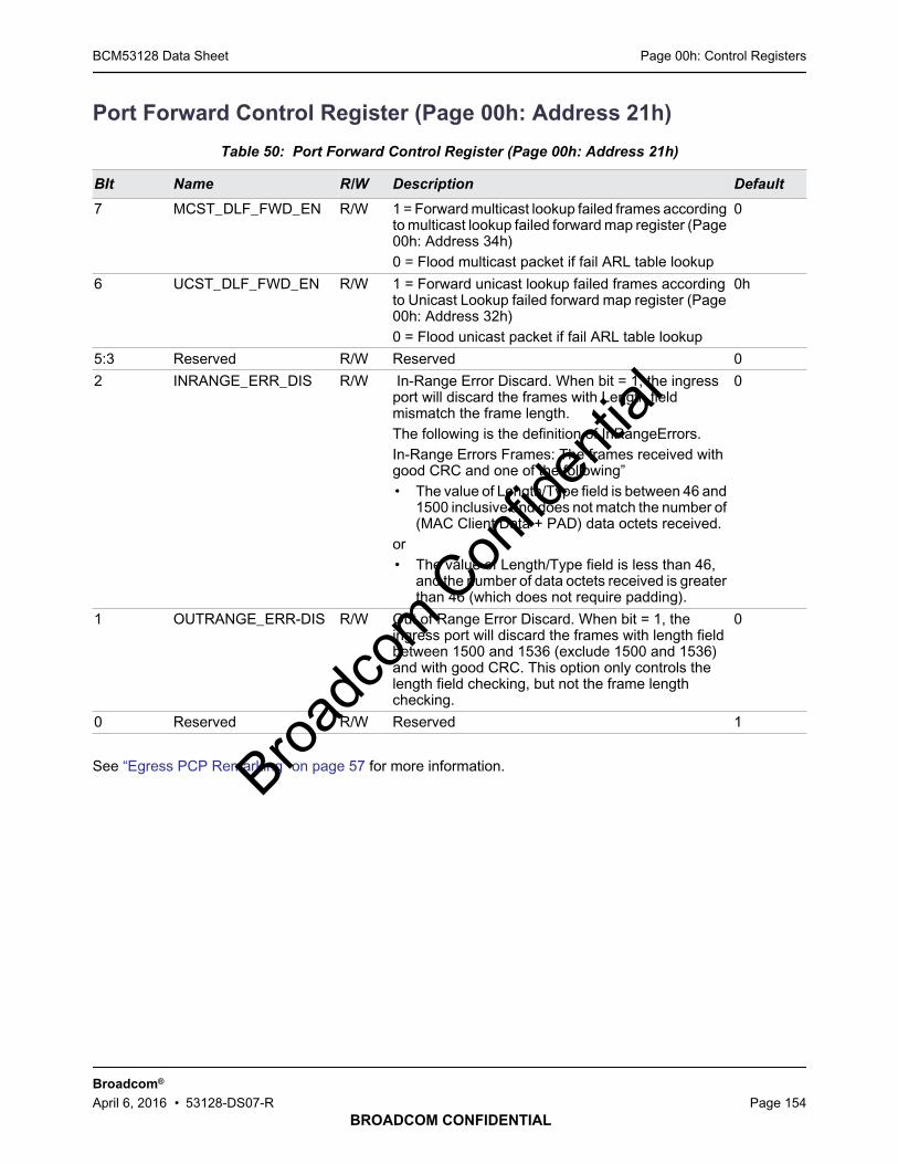
Page 00h: Control RegistersBCM53128 Data Sheet
BROADCOM CONFIDENTIAL
Broadcom®
April 6, 2016 • 53128-DS07-R Page 154
Port Forward Control Register (Page 00h: Address 21h)
See “Egress PCP Remarking” on page 57 for more information.
Table 50: Port Forward Control Register (Page 00h: Address 21h)
BIt Name R/W Description Default
7 MCST_DLF_FWD_EN R/W 1 = Forward multicast lookup failed frames accordingto multicast lookup failed forward map register (Page00h: Address 34h)0 = Flood multicast packet if fail ARL table lookup
0
6 UCST_DLF_FWD_EN R/W 1 = Forward unicast lookup failed frames accordingto Unicast Lookup failed forward map register (Page00h: Address 32h)0 = Flood unicast packet if fail ARL table lookup
0h
5:3 Reserved R/W Reserved 0
2 INRANGE_ERR_DIS R/W In-Range Error Discard. When bit = 1, the ingressport will discard the frames with Length fieldmismatch the frame length.The following is the definition of InRangeErrors.In-Range Errors Frames: The frames received withgood CRC and one of the following”• The value of Length/Type field is between 46 and
1500 inclusive and does not match the number of(MAC Client Data + PAD) data octets received.
or• The value of Length/Type field is less than 46,
and the number of data octets received is greaterthan 46 (which does not require padding).
0
1 OUTRANGE_ERR-DIS R/W Out of Range Error Discard. When bit = 1, theingress port will discard the frames with length fieldbetween 1500 and 1536 (exclude 1500 and 1536)and with good CRC. This option only controls thelength field checking, but not the frame lengthchecking.
0
0 Reserved R/W Reserved 1
Broadc
om C
onfid
entia
l
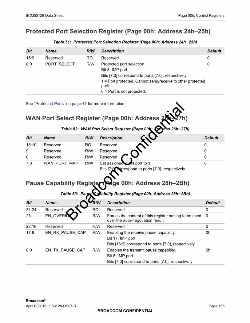
Page 00h: Control RegistersBCM53128 Data Sheet
BROADCOM CONFIDENTIAL
Broadcom®
April 6, 2016 • 53128-DS07-R Page 155
Protected Port Selection Register (Page 00h: Address 24h–25h)
See “Protected Ports” on page 47 for more information.
WAN Port Select Register (Page 00h: Address 26h–27h)
Pause Capability Register (Page 00h: Address 28h–2Bh)
Table 51: Protected Port Selection Register (Page 00h: Address 24h–25h)
BIt Name R/W Description Default
15:9 Reserved RO Reserved 0
8:0 PORT_SELECT R/W Protected port selectionBit 8: IMP portBits [7:0] correspond to ports [7:0], respectively.1 = Port protected. Cannot send/receive to other protectedports.0 = Port is not protected.
0
Table 52: WAN Port Select Register (Page 00h: Address 26h–27h)
BIt Name R/W Description Default
15:10 Reserved RO Reserved 0
9 Reserved R/W Reserved 0
8 Reserved R/W Reserved 0
7:0 WAN_PORT_MAP R/W Set assigned WAN port to 1.Bits [7:0] correspond to ports [7:0], respectively.
0
Table 53: Pause Capability Register (Page 00h: Address 28h–2Bh)
BIt Name R/W Description Default
31:24 Reserved RO Reserved 0
23 EN_OVERIDE R/W Forces the content of this register setting to be usedover the auto-negotiation result.
0
22:18 Reserved R/W Reserved 0
17:9 EN_RX_PAUSE_CAP R/W Enabling the receive pause capability.Bit 17: IMP portBits [16:9] correspond to ports [7:0], respectively.
0h
8:0 EN_TX_PAUSE_CAP R/W Enables the transmit pause capability.Bit 8: IMP portBits [7:0] correspond to ports [7:0], respectively.
0h
Broadc
om C
onfid
entia
l
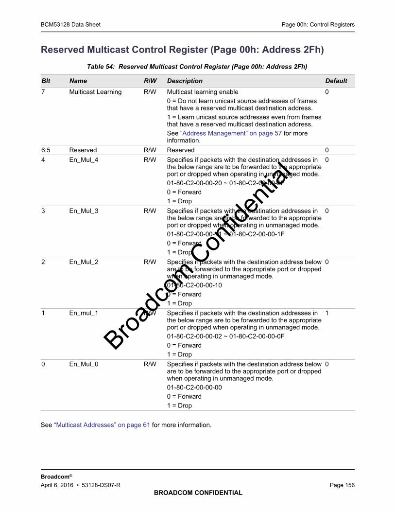
Page 00h: Control RegistersBCM53128 Data Sheet
BROADCOM CONFIDENTIAL
Broadcom®
April 6, 2016 • 53128-DS07-R Page 156
Reserved Multicast Control Register (Page 00h: Address 2Fh)
See “Multicast Addresses” on page 61 for more information.
Table 54: Reserved Multicast Control Register (Page 00h: Address 2Fh)
BIt Name R/W Description Default
7 Multicast Learning R/W Multicast learning enable0 = Do not learn unicast source addresses of framesthat have a reserved multicast destination address.1 = Learn unicast source addresses even from framesthat have a reserved multicast destination address.See “Address Management” on page 57 for moreinformation.
0
6:5 Reserved R/W Reserved 0
4 En_Mul_4 R/W Specifies if packets with the destination addresses inthe below range are to be forwarded to the appropriateport or dropped when operating in unmanaged mode.01-80-C2-00-00-20 ~ 01-80-C2-00-00-2F0 = Forward1 = Drop
0
3 En_Mul_3 R/W Specifies if packets with the destination addresses inthe below range are to be forwarded to the appropriateport or dropped when operating in unmanaged mode.01-80-C2-00-00-11 ~ 01-80-C2-00-00-1F0 = Forward1 = Drop
0
2 En_Mul_2 R/W Specifies if packets with the destination address beloware to be forwarded to the appropriate port or droppedwhen operating in unmanaged mode.01-80-C2-00-00-100 = Forward1 = Drop
0
1 En_mul_1 R/W Specifies if packets with the destination addresses inthe below range are to be forwarded to the appropriateport or dropped when operating in unmanaged mode.01-80-C2-00-00-02 ~ 01-80-C2-00-00-0F0 = Forward1 = Drop
1
0 En_Mul_0 R/W Specifies if packets with the destination address beloware to be forwarded to the appropriate port or droppedwhen operating in unmanaged mode.01-80-C2-00-00-000 = Forward1 = Drop
0
Broadc
om C
onfid
entia
l
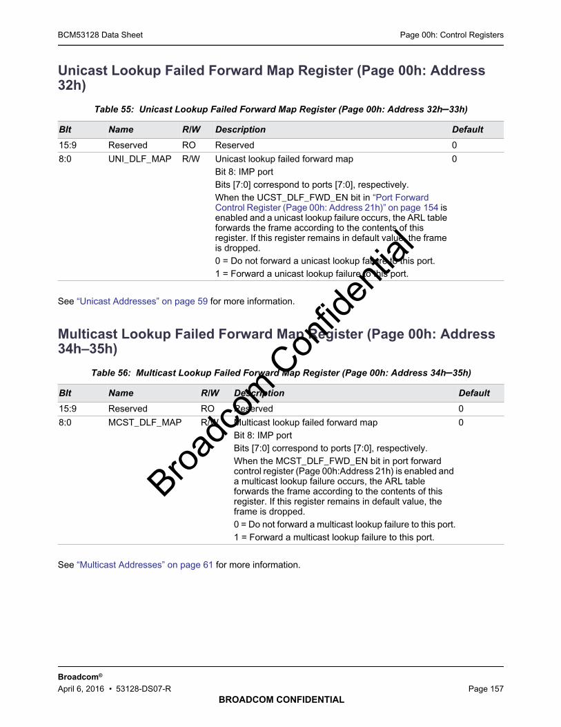
Page 00h: Control RegistersBCM53128 Data Sheet
BROADCOM CONFIDENTIAL
Broadcom®
April 6, 2016 • 53128-DS07-R Page 157
Unicast Lookup Failed Forward Map Register (Page 00h: Address32h)
See “Unicast Addresses” on page 59 for more information.
Multicast Lookup Failed Forward Map Register (Page 00h: Address34h–35h)
See “Multicast Addresses” on page 61 for more information.
Table 55: Unicast Lookup Failed Forward Map Register (Page 00h: Address 32h–33h)
BIt Name R/W Description Default
15:9 Reserved RO Reserved 0
8:0 UNI_DLF_MAP R/W Unicast lookup failed forward mapBit 8: IMP portBits [7:0] correspond to ports [7:0], respectively.When the UCST_DLF_FWD_EN bit in “Port ForwardControl Register (Page 00h: Address 21h)” on page 154 isenabled and a unicast lookup failure occurs, the ARL tableforwards the frame according to the contents of thisregister. If this register remains in default value, the frameis dropped.0 = Do not forward a unicast lookup failure to this port.1 = Forward a unicast lookup failure to this port.
0
Table 56: Multicast Lookup Failed Forward Map Register (Page 00h: Address 34h–35h)
BIt Name R/W Description Default
15:9 Reserved RO Reserved 0
8:0 MCST_DLF_MAP R/W Multicast lookup failed forward mapBit 8: IMP portBits [7:0] correspond to ports [7:0], respectively.When the MCST_DLF_FWD_EN bit in port forwardcontrol register (Page 00h:Address 21h) is enabled anda multicast lookup failure occurs, the ARL tableforwards the frame according to the contents of thisregister. If this register remains in default value, theframe is dropped.0 = Do not forward a multicast lookup failure to this port.1 = Forward a multicast lookup failure to this port.
0
Broadc
om C
onfid
entia
l
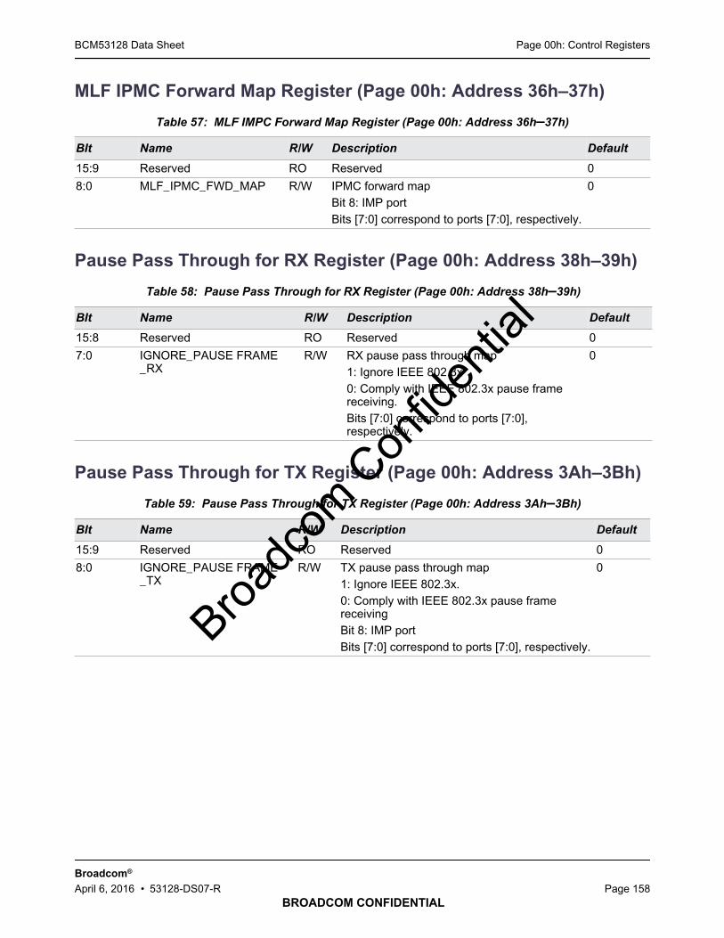
Page 00h: Control RegistersBCM53128 Data Sheet
BROADCOM CONFIDENTIAL
Broadcom®
April 6, 2016 • 53128-DS07-R Page 158
MLF IPMC Forward Map Register (Page 00h: Address 36h–37h)
Pause Pass Through for RX Register (Page 00h: Address 38h–39h)
Pause Pass Through for TX Register (Page 00h: Address 3Ah–3Bh)
Table 57: MLF IMPC Forward Map Register (Page 00h: Address 36h–37h)
BIt Name R/W Description Default
15:9 Reserved RO Reserved 0
8:0 MLF_IPMC_FWD_MAP R/W IPMC forward mapBit 8: IMP portBits [7:0] correspond to ports [7:0], respectively.
0
Table 58: Pause Pass Through for RX Register (Page 00h: Address 38h–39h)
BIt Name R/W Description Default
15:8 Reserved RO Reserved 0
7:0 IGNORE_PAUSE FRAME_RX
R/W RX pause pass through map1: Ignore IEEE 802.3x0: Comply with IEEE 802.3x pause framereceiving.Bits [7:0] correspond to ports [7:0],respectively.
0
Table 59: Pause Pass Through for TX Register (Page 00h: Address 3Ah–3Bh)
BIt Name R/W Description Default
15:9 Reserved RO Reserved 0
8:0 IGNORE_PAUSE FRAME_TX
R/W TX pause pass through map1: Ignore IEEE 802.3x.0: Comply with IEEE 802.3x pause framereceivingBit 8: IMP portBits [7:0] correspond to ports [7:0], respectively.
0
Broadc
om C
onfid
entia
l
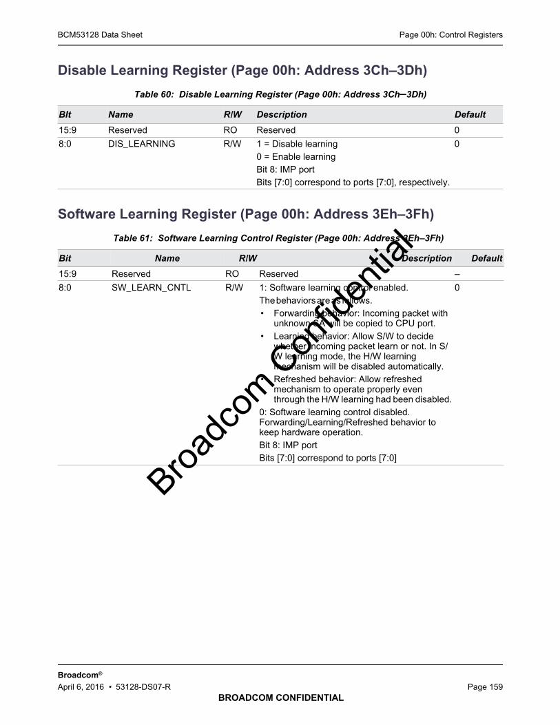
Page 00h: Control RegistersBCM53128 Data Sheet
BROADCOM CONFIDENTIAL
Broadcom®
April 6, 2016 • 53128-DS07-R Page 159
Disable Learning Register (Page 00h: Address 3Ch–3Dh)
Software Learning Register (Page 00h: Address 3Eh–3Fh)
Table 60: Disable Learning Register (Page 00h: Address 3Ch–3Dh)
BIt Name R/W Description Default
15:9 Reserved RO Reserved 0
8:0 DIS_LEARNING R/W 1 = Disable learning0 = Enable learningBit 8: IMP portBits [7:0] correspond to ports [7:0], respectively.
0
Table 61: Software Learning Control Register (Page 00h: Address 3Eh–3Fh)
Bit Name R/W Description Default
15:9 Reserved RO Reserved –
8:0 SW_LEARN_CNTL R/W 1: Software learning control enabled.Thebehaviorsareasfollows.• Forwarding behavior: Incoming packet with
unknown SA will be copied to CPU port.• Learning behavior: Allow S/W to decide
whether incoming packet learn or not. In S/W learning mode, the H/W learningmechanism will be disabled automatically.
• Refreshed behavior: Allow refreshedmechanism to operate properly eventhrough the H/W learning had been disabled.
0: Software learning control disabled.Forwarding/Learning/Refreshed behavior tokeep hardware operation.Bit 8: IMP portBits [7:0] correspond to ports [7:0]
0
Broadc
om C
onfid
entia
l

Page 00h: Control RegistersBCM53128 Data Sheet
BROADCOM CONFIDENTIAL
Broadcom®
April 6, 2016 • 53128-DS07-R Page 160
Port State Override Register (Page 00h: Address 58h)
Table 62: Port State Override Register Address Summary
Address Description
58h Port 0
59h Port 1
5Ah Port 2
5Bh Port 3
5Ch Port 4
5Dh Port 5
5Eh Port 6
5Fh Port 7
Table 63: Port State Override Register (Page 00h: Address 58h–5Fh)
BIt Name R/W Description Default
7 Reserved R/W Reserved –
6 Software Override R/W Writing 1 to this bit allows the values of the bits [7:0]to be written to the external PHY. Writing 0 to thisbit prevents these values from overriding thepresent external PHY conditions.
0
5 TXFlow Control Enable R/W The value of this bit overrides the existingconditions of the external PHY port if bit 6 is writtento 1.0 = Flow control disabled for transmit traffic.1 = Flow control enabled for transmit traffic.
0
4 RX Flow Control Enable R/W The value of this bit overrides the existingconditions of the external PHY port if bit 6 is writtento 1.0 = Flow control disabled for receive traffic.1 = Flow control enabled for receive traffic.
0
3:2 Speed R/W The value of this bit overrides the existingconditions of the external PHY port if bit 6 is writtento 1.00 = 10 Mbps01 = 100 Mbps10 = 1000 Mbps11 = Illegal state
10
1 Duplex Mode R/W The value of this bit overrides the existingconditions of the external PHY port if bit 6 is writtento 1.0 = Half-duplex1 = Full-duplex
1
Broadc
om C
onfid
entia
l
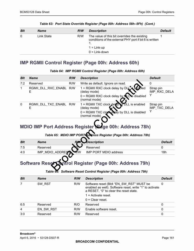
Page 00h: Control RegistersBCM53128 Data Sheet
BROADCOM CONFIDENTIAL
Broadcom®
April 6, 2016 • 53128-DS07-R Page 161
IMP RGMII Control Register (Page 00h: Address 60h)
MDIO IMP Port Address Register (Page 00h: Address 78h)
Software Reset Control Register (Page 00h: Address 79h)
0 Link State R/W The value of this bit overrides the existingconditions of the external PHY port if bit 6 is written1.1 = Link-up0 = Link-down
1
Table 64: IMP RGMII Control Register (Page 00h: Address 60h)
BIt Name R/W Description Default
7:2 Reserved R/W Write as default. Ignore on read. 0
1 RGMII_DLL_RXC_ENABLE
R/W 1 = RGMII RXC clock delay by DLL is enabled(delay mode)0 = RGMII RXC clock delay by DLL is disabled(normal mode)
Strap pinIMP_RXC_DELAY
0 RGMII_DLL_TXC_ENABLE
R/W 1 = RGMII TXC clock delay by DLL is enabled(delay mode)0 = RGMII TXC clock delay by DLL is disabled(normal mode)
Strap pinIMP_TXC_DELAY
Table 65: MDIO IMP PORT Address Register (Page 00h: Address 78h)
BIt Name R/W Description Default
7:5 Reserved RO Reserved 0
4:0 IMP_MDIO_ADDRESS R/W IMP PORT MDIO address 18h
Table 66: Software Reset Control Register (Page 00h: Address 79h)
BIt Name R/W Description Default
7 SW_RST R/W Software reset (Bit4 “EN_SW_RST” MUST beenabled as well). Software reset, write “1” to activatea RESET, “0” to clear the reset state.1 = Activate reset.0 = Clear reset.
0
6:5 Reserved R/O Reserved 0
4 EN_SW_RST R/W Enable software reset. 0
3:0 Reserved R/W Reserved 0
Table 63: Port State Override Register (Page 00h: Address 58h–5Fh) (Cont.)
BIt Name R/W Description Default
Broadc
om C
onfid
entia
l
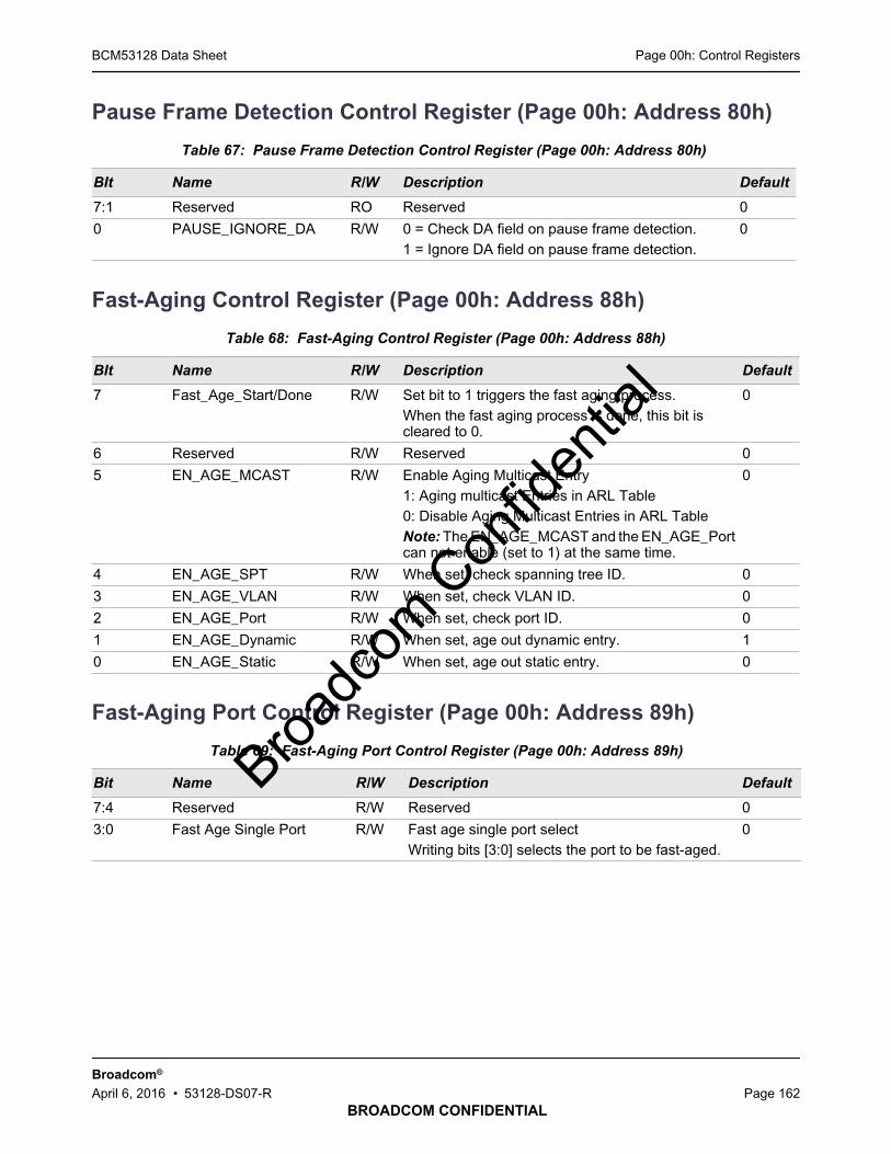
Page 00h: Control RegistersBCM53128 Data Sheet
BROADCOM CONFIDENTIAL
Broadcom®
April 6, 2016 • 53128-DS07-R Page 162
Pause Frame Detection Control Register (Page 00h: Address 80h)
Fast-Aging Control Register (Page 00h: Address 88h)
Fast-Aging Port Control Register (Page 00h: Address 89h)
Table 67: Pause Frame Detection Control Register (Page 00h: Address 80h)
BIt Name R/W Description Default
7:1 Reserved RO Reserved 0
0 PAUSE_IGNORE_DA R/W 0 = Check DA field on pause frame detection.1 = Ignore DA field on pause frame detection.
0
Table 68: Fast-Aging Control Register (Page 00h: Address 88h)
BIt Name R/W Description Default
7 Fast_Age_Start/Done R/W Set bit to 1 triggers the fast aging process.When the fast aging process is done, this bit iscleared to 0.
0
6 Reserved R/W Reserved 0
5 EN_AGE_MCAST R/W Enable Aging Multicast Entry1: Aging multicast Entries in ARL Table0: Disable Aging Multicast Entries in ARL TableNote: The EN_AGE_MCAST and the EN_AGE_Portcan not enable (set to 1) at the same time.
0
4 EN_AGE_SPT R/W When set, check spanning tree ID. 0
3 EN_AGE_VLAN R/W When set, check VLAN ID. 0
2 EN_AGE_Port R/W When set, check port ID. 0
1 EN_AGE_Dynamic R/W When set, age out dynamic entry. 1
0 EN_AGE_Static R/W When set, age out static entry. 0
Table 69: Fast-Aging Port Control Register (Page 00h: Address 89h)
Bit Name R/W Description Default
7:4 Reserved R/W Reserved 0
3:0 Fast Age Single Port R/W Fast age single port selectWriting bits [3:0] selects the port to be fast-aged.
0
Broadc
om C
onfid
entia
l

Page 00h: Control RegistersBCM53128 Data Sheet
BROADCOM CONFIDENTIAL
Broadcom®
April 6, 2016 • 53128-DS07-R Page 163
Fast-Aging VID Control Register (Page 00h: Address 8Ah–8Bh)
CPU Data 0 Share Register (Page 00h: Address B0h-B7h)
.
CPU Data 1 Share Register (Page 00h: Address B8h-BFh)
.
Table 70: Fast-Aging VID Control Register (Page 00h: Address 8Ah–8Bh)
Bit Name R/W Description Default
15:12 Reserved R/W Reserved 0
11:0 Fast Age Single VID R/W Fast age single VID selectWriting bits [11:0] selects the VID to be fast-aged.
0
Table 71: CPU Data 0 Share Register (Page 00h: Address B0h–B7h)
Bit Name R/W Description Default
63:0 CPU_DATA_SHARE R/W Data to be shared by internal 8051 and externalCPU
0x0
Table 72: CPU Data 1 Share Register (Page 00h: Address B8h–BFh)
Bit Name R/W Description Default
63:0 CPU_DATA_SHARE R/W Data to be shared by internal 8051 and externalCPU
0x0
Broadc
om C
onfid
entia
l
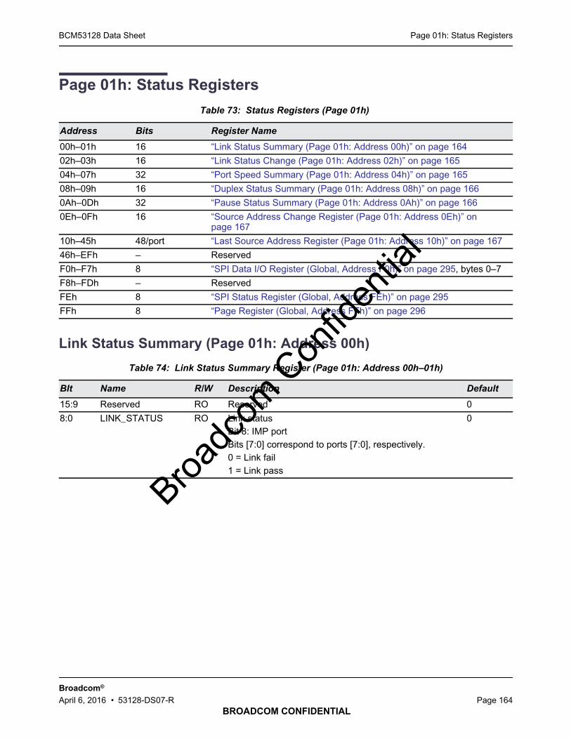
Page 01h: Status RegistersBCM53128 Data Sheet
BROADCOM CONFIDENTIAL
Broadcom®
April 6, 2016 • 53128-DS07-R Page 164
Page 01h: Status Registers
Link Status Summary (Page 01h: Address 00h)
Table 73: Status Registers (Page 01h)
Address Bits Register Name
00h–01h 16 “Link Status Summary (Page 01h: Address 00h)” on page 164
02h–03h 16 “Link Status Change (Page 01h: Address 02h)” on page 165
04h–07h 32 “Port Speed Summary (Page 01h: Address 04h)” on page 165
08h–09h 16 “Duplex Status Summary (Page 01h: Address 08h)” on page 166
0Ah–0Dh 32 “Pause Status Summary (Page 01h: Address 0Ah)” on page 166
0Eh–0Fh 16 “Source Address Change Register (Page 01h: Address 0Eh)” onpage 167
10h–45h 48/port “Last Source Address Register (Page 01h: Address 10h)” on page 167
46h–EFh – Reserved
F0h–F7h 8 “SPI Data I/O Register (Global, Address F0h)” on page 295, bytes 0–7
F8h–FDh – Reserved
FEh 8 “SPI Status Register (Global, Address FEh)” on page 295
FFh 8 “Page Register (Global, Address FFh)” on page 296
Table 74: Link Status Summary Register (Page 01h: Address 00h–01h)
BIt Name R/W Description Default
15:9 Reserved RO Reserved 0
8:0 LINK_STATUS RO Link statusBit 8: IMP portBits [7:0] correspond to ports [7:0], respectively.0 = Link fail1 = Link pass
0
Broadc
om C
onfid
entia
l

Page 01h: Status RegistersBCM53128 Data Sheet
BROADCOM CONFIDENTIAL
Broadcom®
April 6, 2016 • 53128-DS07-R Page 165
Link Status Change (Page 01h: Address 02h)
Port Speed Summary (Page 01h: Address 04h)
Table 75: Link Status Change Register (Page 01h: Address 02h–03h)
BIt Name R/W Description Default
15:9 Reserved RO Reserved 0
8:0 LINK_STATUS_CHANGE RO Link status change.Bit 8: IMP portBits [7:0] correspond to ports [7:0], respectively.Upon change of link status, a bit remains set untilcleared by a read operation.0 = Link status constant.1 = Link status change.
0x1FF
Table 76: Port Speed Summary Register (Page 01h: Address 04h–07h)
BIt Name R/W Description Default
31:18 Reserved PO Reserved 0
17:0 PORT_SPEED RO Port speedThe speed of each port is reported based on the mappingbelow:• Bits [17:16] = IMP port• Bits [15:14] = Port 7• Bits [13:12] = Port 6• Bits [11:10] = Port 5• Bits [9:8] = Port 4• Bits [7:6] = Port 3• Bits [5:4] = Port 2• Bits [3:2] = Port 1• Bits [1:0] = Port 0The value of the bits are:• 00 = 10 Mbps• 01 = 100 Mbps• 10 = 1000 Mbps• 11 = 200 Mbps (for IMP port only)
0x2AAAA
Broadc
om C
onfid
entia
l
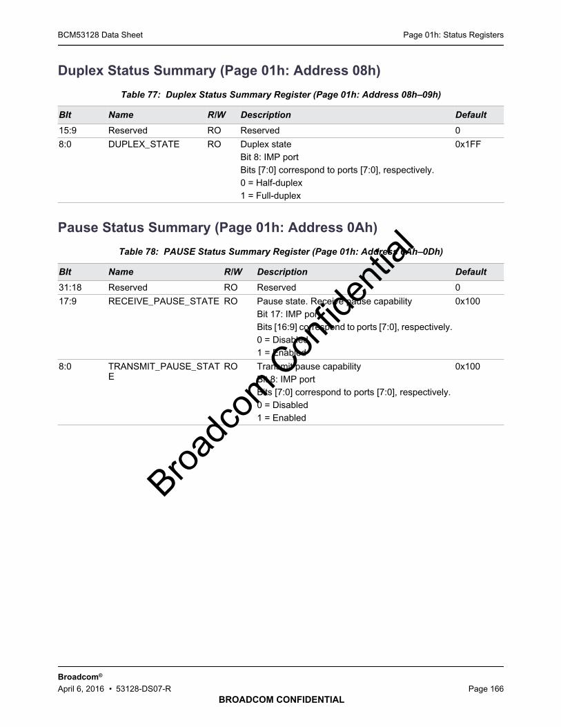
Page 01h: Status RegistersBCM53128 Data Sheet
BROADCOM CONFIDENTIAL
Broadcom®
April 6, 2016 • 53128-DS07-R Page 166
Duplex Status Summary (Page 01h: Address 08h)
Pause Status Summary (Page 01h: Address 0Ah)
Table 77: Duplex Status Summary Register (Page 01h: Address 08h–09h)
BIt Name R/W Description Default
15:9 Reserved RO Reserved 0
8:0 DUPLEX_STATE RO Duplex stateBit 8: IMP portBits [7:0] correspond to ports [7:0], respectively.0 = Half-duplex1 = Full-duplex
0x1FF
Table 78: PAUSE Status Summary Register (Page 01h: Address 0Ah–0Dh)
BIt Name R/W Description Default
31:18 Reserved RO Reserved 0
17:9 RECEIVE_PAUSE_STATE RO Pause state. Receive pause capabilityBit 17: IMP portBits [16:9] correspond to ports [7:0], respectively.0 = Disabled1 = Enabled
0x100
8:0 TRANSMIT_PAUSE_STATE
RO Transmit pause capabilityBit 8: IMP portBits [7:0] correspond to ports [7:0], respectively.0 = Disabled1 = Enabled
0x100
Broadc
om C
onfid
entia
l
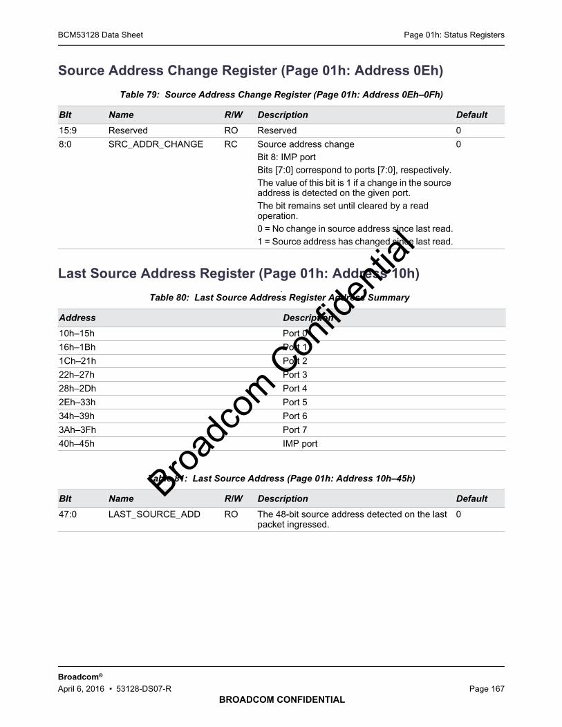
Page 01h: Status RegistersBCM53128 Data Sheet
BROADCOM CONFIDENTIAL
Broadcom®
April 6, 2016 • 53128-DS07-R Page 167
Source Address Change Register (Page 01h: Address 0Eh)
Last Source Address Register (Page 01h: Address 10h).
Table 79: Source Address Change Register (Page 01h: Address 0Eh–0Fh)
BIt Name R/W Description Default
15:9 Reserved RO Reserved 0
8:0 SRC_ADDR_CHANGE RC Source address changeBit 8: IMP portBits [7:0] correspond to ports [7:0], respectively.The value of this bit is 1 if a change in the sourceaddress is detected on the given port.The bit remains set until cleared by a readoperation.0 = No change in source address since last read.1 = Source address has changed since last read.
0
Table 80: Last Source Address Register Address Summary
Address Description
10h–15h Port 0
16h–1Bh Port 1
1Ch–21h Port 2
22h–27h Port 3
28h–2Dh Port 4
2Eh–33h Port 5
34h–39h Port 6
3Ah–3Fh Port 7
40h–45h IMP port
Table 81: Last Source Address (Page 01h: Address 10h–45h)
BIt Name R/W Description Default
47:0 LAST_SOURCE_ADD RO The 48-bit source address detected on the lastpacket ingressed.
0
Broadc
om C
onfid
entia
l
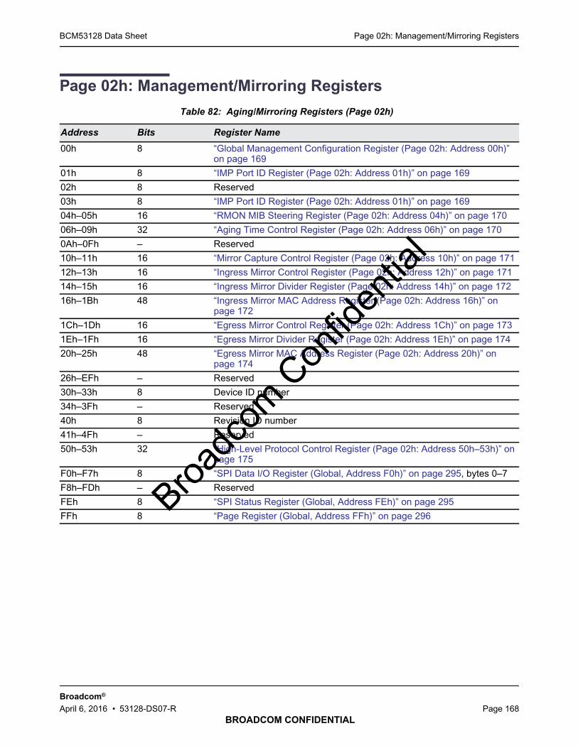
Page 02h: Management/Mirroring RegistersBCM53128 Data Sheet
BROADCOM CONFIDENTIAL
Broadcom®
April 6, 2016 • 53128-DS07-R Page 168
Page 02h: Management/Mirroring Registers
Table 82: Aging/Mirroring Registers (Page 02h)
Address Bits Register Name
00h 8 “Global Management Configuration Register (Page 02h: Address 00h)”on page 169
01h 8 “IMP Port ID Register (Page 02h: Address 01h)” on page 169
02h 8 Reserved
03h 8 “IMP Port ID Register (Page 02h: Address 01h)” on page 169
04h–05h 16 “RMON MIB Steering Register (Page 02h: Address 04h)” on page 170
06h–09h 32 “Aging Time Control Register (Page 02h: Address 06h)” on page 170
0Ah–0Fh – Reserved
10h–11h 16 “Mirror Capture Control Register (Page 02h: Address 10h)” on page 171
12h–13h 16 “Ingress Mirror Control Register (Page 02h: Address 12h)” on page 171
14h–15h 16 “Ingress Mirror Divider Register (Page 02h: Address 14h)” on page 172
16h–1Bh 48 “Ingress Mirror MAC Address Register (Page 02h: Address 16h)” onpage 172
1Ch–1Dh 16 “Egress Mirror Control Register (Page 02h: Address 1Ch)” on page 173
1Eh–1Fh 16 “Egress Mirror Divider Register (Page 02h: Address 1Eh)” on page 174
20h–25h 48 “Egress Mirror MAC Address Register (Page 02h: Address 20h)” onpage 174
26h–EFh – Reserved
30h–33h 8 Device ID number
34h–3Fh – Reserved
40h 8 Revision ID number
41h–4Fh – Reserved
50h–53h 32 “High-Level Protocol Control Register (Page 02h: Address 50h–53h)” onpage 175
F0h–F7h 8 “SPI Data I/O Register (Global, Address F0h)” on page 295, bytes 0–7
F8h–FDh – Reserved
FEh 8 “SPI Status Register (Global, Address FEh)” on page 295
FFh 8 “Page Register (Global, Address FFh)” on page 296Broa
dcom
Con
fiden
tial

Page 02h: Management/Mirroring RegistersBCM53128 Data Sheet
BROADCOM CONFIDENTIAL
Broadcom®
April 6, 2016 • 53128-DS07-R Page 169
Global Management Configuration Register (Page 02h: Address 00h)
IMP Port ID Register (Page 02h: Address 01h)
Table 83: Global Management Configuration Register (Page 02h: Address 00h)
Bit Name R/W Description Default
7:6 En_IMP_Port R/W IMP port enable00 = No frame management port.01 = Reserved10 = Enable IMP port only. All traffic to CPU from LANand WAN ports will be forwarded to IMP port.11 = ReservedThese bits are ignored when SW_FWD_MODE =Unmanaged in the “Switch Mode Register (Page 00h:Address 0Bh)” on page 148.
00
5 Reserved R/W Reserved 0
4 Reserved R/W Reserved 0
3:2 Reserved R/W Reserved 0
1 En_Rx_BPDU R/W Receive BPDU enableEnables all ports to receive BPDUs and forwards to theIMP port. This bit must be set to globally allow BPDUsto be received.
0
0 Reset MIB R/W Reset MIB countersResets all MIB counters for all ports to 0 (pages 20h–28h). This bit must be set and then cleared insuccessive write cycles to activate the reset operation.
0
Table 84: IMP Port ID Register (Page 02h: Address 01h)
Bit Name R/W Description Default
7:4 Reserved RO Reserved 0x0
3:0 IMP_PRT_ID RO IMP Port IDThe field specifies the port ID of the IMP port. TheBCM53128 IMP is fixed at Port 8.
0x8
Broadc
om C
onfid
entia
l

Page 02h: Management/Mirroring RegistersBCM53128 Data Sheet
BROADCOM CONFIDENTIAL
Broadcom®
April 6, 2016 • 53128-DS07-R Page 170
Broadcom Header Control Register (Page 02h: Address 03h)
RMON MIB Steering Register (Page 02h: Address 04h)
Aging Time Control Register (Page 02h: Address 06h)
Table 85: Broadcom Tag Control Register (Page 02h: Address 03h)
Bit Name R/W Description Default
7:1 Reserved RO Reserved 0
0 BRCM_HDR_EN R/W Broadcom Tag enable for IMP. Enable Broadcom header forIMP port.1 = Additional header information is inserted into the originalframe, between original SA field and Type/Length fields.The tag includes the Broadcom Tag field.0 = Without additional header information.
1
Table 86: RMON MIB Steering Register (Page 02h: Address 04h–05h)
Bit Name R/W Description Default
15:9 Reserved R/W Reserved 0
8:0 Override RMONReceive
R/W Override RMON receiveForces the RMON packet size bucket counters from thenormal default of snooping on the receive side of the MACto the transmit side. This allows the RMON bucket countersto snoop either transmit or receive, allowing full-duplexMAC support.Bit 8: IMP portBits [7:0] correspond to ports [7:0], respectively.
0
Table 87: Aging Time Control Register (Page 02h: Address 06h–09h)
BIt Name R/W Description Default
31:21 Reserved RO Reserved 0
20 Age Change R/W Age change enable1 = Set age time via bits [19:0] immediately.0 = Age time will be changed by the new value specifiedin bit[19:0], after the original age time value in bit[19:0]times up.
0
19:0 AGE_TIME R/W Specifies the aging time in seconds for dynamicallylearned addresses. Maximum age time is 1,048,575s.Setting the AGE_TIME to 0 disables the aging process.For more information on ARL table aging, see “AddressAging” on page 64.
300d
Broadc
om C
onfid
entia
l
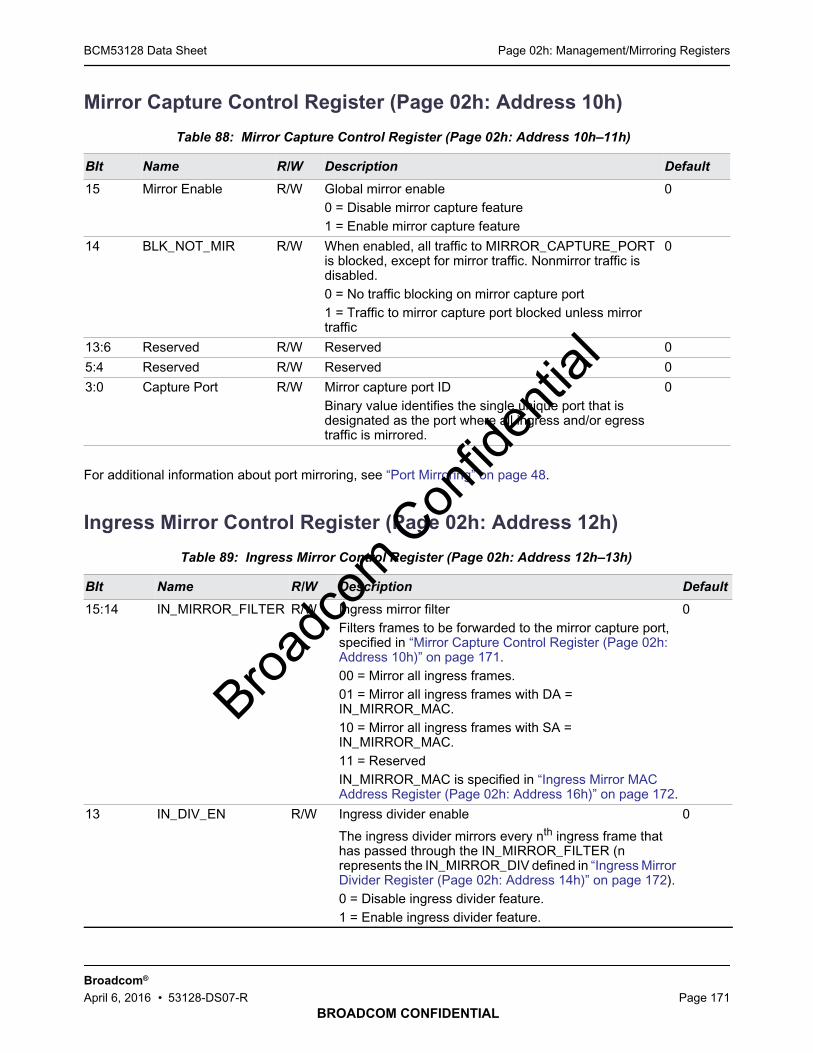
Page 02h: Management/Mirroring RegistersBCM53128 Data Sheet
BROADCOM CONFIDENTIAL
Broadcom®
April 6, 2016 • 53128-DS07-R Page 171
Mirror Capture Control Register (Page 02h: Address 10h)
For additional information about port mirroring, see “Port Mirroring” on page 48.
Ingress Mirror Control Register (Page 02h: Address 12h)
Table 88: Mirror Capture Control Register (Page 02h: Address 10h–11h)
BIt Name R/W Description Default
15 Mirror Enable R/W Global mirror enable0 = Disable mirror capture feature1 = Enable mirror capture feature
0
14 BLK_NOT_MIR R/W When enabled, all traffic to MIRROR_CAPTURE_PORTis blocked, except for mirror traffic. Nonmirror traffic isdisabled.0 = No traffic blocking on mirror capture port1 = Traffic to mirror capture port blocked unless mirrortraffic
0
13:6 Reserved R/W Reserved 0
5:4 Reserved R/W Reserved 0
3:0 Capture Port R/W Mirror capture port IDBinary value identifies the single unique port that isdesignated as the port where all ingress and/or egresstraffic is mirrored.
0
Table 89: Ingress Mirror Control Register (Page 02h: Address 12h–13h)
BIt Name R/W Description Default
15:14 IN_MIRROR_FILTER R/W Ingress mirror filterFilters frames to be forwarded to the mirror capture port,specified in “Mirror Capture Control Register (Page 02h:Address 10h)” on page 171.00 = Mirror all ingress frames.01 = Mirror all ingress frames with DA =IN_MIRROR_MAC.10 = Mirror all ingress frames with SA =IN_MIRROR_MAC.11 = ReservedIN_MIRROR_MAC is specified in “Ingress Mirror MACAddress Register (Page 02h: Address 16h)” on page 172.
0
13 IN_DIV_EN R/W Ingress divider enable
The ingress divider mirrors every nth ingress frame thathas passed through the IN_MIRROR_FILTER (nrepresents the IN_MIRROR_DIV defined in “Ingress MirrorDivider Register (Page 02h: Address 14h)” on page 172).0 = Disable ingress divider feature.1 = Enable ingress divider feature.
0
Broadc
om C
onfid
entia
l
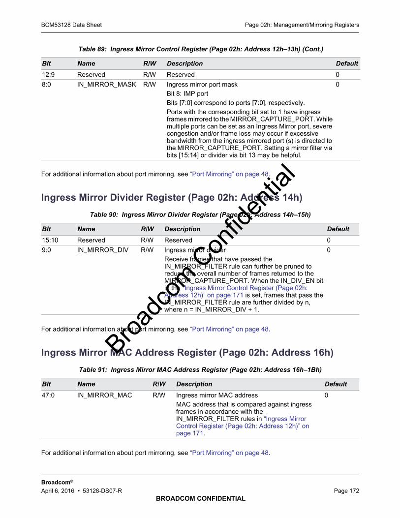
Page 02h: Management/Mirroring RegistersBCM53128 Data Sheet
BROADCOM CONFIDENTIAL
Broadcom®
April 6, 2016 • 53128-DS07-R Page 172
For additional information about port mirroring, see “Port Mirroring” on page 48.
Ingress Mirror Divider Register (Page 02h: Address 14h)
For additional information about port mirroring, see “Port Mirroring” on page 48.
Ingress Mirror MAC Address Register (Page 02h: Address 16h)
For additional information about port mirroring, see “Port Mirroring” on page 48.
12:9 Reserved R/W Reserved 0
8:0 IN_MIRROR_MASK R/W Ingress mirror port maskBit 8: IMP portBits [7:0] correspond to ports [7:0], respectively.Ports with the corresponding bit set to 1 have ingressframes mirrored to the MIRROR_CAPTURE_PORT. Whilemultiple ports can be set as an Ingress Mirror port, severecongestion and/or frame loss may occur if excessivebandwidth from the ingress mirrored port (s) is directed tothe MIRROR_CAPTURE_PORT. Setting a mirror filter viabits [15:14] or divider via bit 13 may be helpful.
0
Table 90: Ingress Mirror Divider Register (Page 02h: Address 14h–15h)
BIt Name R/W Description Default
15:10 Reserved R/W Reserved 0
9:0 IN_MIRROR_DIV R/W Ingress mirror dividerReceive frames that have passed theIN_MIRROR_FILTER rule can further be pruned toreduce the overall number of frames returned to theMIRROR_CAPTURE_PORT. When the IN_DIV_EN bitin the “Ingress Mirror Control Register (Page 02h:Address 12h)” on page 171 is set, frames that pass theIN_MIRROR_FILTER rule are further divided by n,where n = IN_MIRROR_DIV + 1.
0
Table 91: Ingress Mirror MAC Address Register (Page 02h: Address 16h–1Bh)
BIt Name R/W Description Default
47:0 IN_MIRROR_MAC R/W Ingress mirror MAC addressMAC address that is compared against ingressframes in accordance with theIN_MIRROR_FILTER rules in “Ingress MirrorControl Register (Page 02h: Address 12h)” onpage 171.
0
Table 89: Ingress Mirror Control Register (Page 02h: Address 12h–13h) (Cont.)
BIt Name R/W Description Default
Broadc
om C
onfid
entia
l

Page 02h: Management/Mirroring RegistersBCM53128 Data Sheet
BROADCOM CONFIDENTIAL
Broadcom®
April 6, 2016 • 53128-DS07-R Page 173
Egress Mirror Control Register (Page 02h: Address 1Ch)
For additional information about port mirroring, see “Port Mirroring” on page 48.
Table 92: Egress Mirror Control Register (Page 02h: Address 1Ch–1Dh)
BIt Name R/W Description Default
15:14 OUT_MIRROR_FILTER
R/W Egress mirror filterFilters egress frames that are forwarded to the mirrorcapture port, specified in “Mirror Capture ControlRegister (Page 02h: Address 10h)” on page 171.00 = Mirror all egress frames.01 = Mirror all egress frames with DA =OUT_MIRROR_MAC.10 = Mirror all egress frames with SA =OUT_MIRROR_MAC.11 = Reserved.OUT_MIRROR_MAC is specified in “Egress Mirror MACAddress Register (Page 02h: Address 20h)” onpage 174.
0
13 OUT_DIV_EN R/W Egress divider enable
The egress divider mirrors every nth egress frame thathas passed through the OUT_MIRROR_FILTER (nrepresents the OUT_MIRROR_DIV defined in “EgressMirror Divider Register (Page 02h: Address 1Eh)” onpage 174).0 = Disable egress divider feature.1 = Enable egress divider feature.
0
12:9 Reserved R/W Reserved 0
8:0 OUT_MIRROR_MASK R/W Egress mirror port maskBit 8: IMP portBits [7:0] correspond to ports [7:0], respectively.Ports with the corresponding bit set to 1 have egressframes mirrored to the MIRROR_CAPTURE_PORT.While multiple ports can be set as an egress mirror port,severe congestion and/or frame loss may occur ifexcessive bandwidth from the egress mirrored port (s) isdirected to the MIRROR_CAPTURE_PORT. Setting amirror filter via bits [15:14] or a divider via bit 13 may behelpful.
0
Broadc
om C
onfid
entia
l
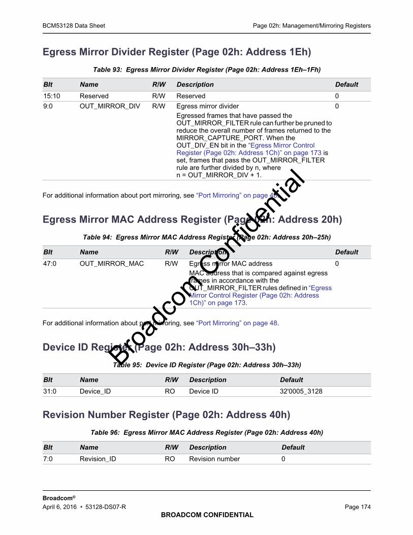
Page 02h: Management/Mirroring RegistersBCM53128 Data Sheet
BROADCOM CONFIDENTIAL
Broadcom®
April 6, 2016 • 53128-DS07-R Page 174
Egress Mirror Divider Register (Page 02h: Address 1Eh)
For additional information about port mirroring, see “Port Mirroring” on page 48.
Egress Mirror MAC Address Register (Page 02h: Address 20h)
For additional information about port mirroring, see “Port Mirroring” on page 48.
Device ID Register (Page 02h: Address 30h–33h)
Revision Number Register (Page 02h: Address 40h)
Table 93: Egress Mirror Divider Register (Page 02h: Address 1Eh–1Fh)
BIt Name R/W Description Default
15:10 Reserved R/W Reserved 0
9:0 OUT_MIRROR_DIV R/W Egress mirror dividerEgressed frames that have passed theOUT_MIRROR_FILTER rule can further be pruned toreduce the overall number of frames returned to theMIRROR_CAPTURE_PORT. When theOUT_DIV_EN bit in the “Egress Mirror ControlRegister (Page 02h: Address 1Ch)” on page 173 isset, frames that pass the OUT_MIRROR_FILTERrule are further divided by n, wheren = OUT_MIRROR_DIV + 1.
0
Table 94: Egress Mirror MAC Address Register (Page 02h: Address 20h–25h)
BIt Name R/W Description Default
47:0 OUT_MIRROR_MAC R/W Egress mirror MAC addressMAC address that is compared against egressframes in accordance with theOUT_MIRROR_FILTER rules defined in “EgressMirror Control Register (Page 02h: Address1Ch)” on page 173.
0
Table 95: Device ID Register (Page 02h: Address 30h–33h)
BIt Name R/W Description Default
31:0 Device_ID RO Device ID 32'0005_3128
Table 96: Egress Mirror MAC Address Register (Page 02h: Address 40h)
BIt Name R/W Description Default
7:0 Revision_ID RO Revision number 0
Broadc
om C
onfid
entia
l

Page 02h: Management/Mirroring RegistersBCM53128 Data Sheet
BROADCOM CONFIDENTIAL
Broadcom®
April 6, 2016 • 53128-DS07-R Page 175
High-Level Protocol Control Register (Page 02h: Address 50h–53h)
Table 97: High-Level Protocol Control Register (Page 02h: Address 50h–53h)
BIt Name R/W Description Default
31:19 Reserved R/W Reserved –
18 MLD_QRY_FWD_MODE R/W MLD Query Message Forwarding Mode1: MLD Query message frames will be trapped toCPU port only.0: MLD Query message frames will be forwardedby L2 result and also copied to CPU.
0
17 MLD_QRY_EN R/W MLD Query Message Snooping/Redirect Enable1: Enable MLD query message snooping/redirect0: Disable
0
16 MLD_RPTDONE_FWD_MODE
R/W MLDReport/DoneMessageForwardingMode1: MLD report/done message frames will betrapped to CPU port only0: MLD report/done message frames will beforwarded by L2 result and also copied to CPU
0
15 MLD_RPTDONE_EN R/W MLD Report/Done Message Snooping/RedirectEnable1: Enable MLD report/done message snooping/redirect0: Disable
0
14 IGMP_UKN_FWD_MODE R/W IGMP Unknown Message Forwarding Mode1: IGMP unknown message frames will betrapped to CPU port only0: IGMP unknown message frames will beforwarded by L2 result and also copied to CPU
0
13 IGMP_UKN_EN R/W IGMP Unknown Message Snooping/RedirectEnable1: Enable IGMP unknown message snooping/redirect0: Disable
0
12 IGMP_QRY_FWD_MODE R/W IGMP Query Message Forwarding Mode1: IGMP query message frames will be trappedto CPU port only0: IGMP query message frames will beforwarded by L2 result and also copied to CPU
0
11 IGMP_QRY_EN R/W IGMP Query Message Snooping/RedirectEnable1: Enable IGMP query message Snooping/Redirect0: Disable
0
Broadc
om C
onfid
entia
l
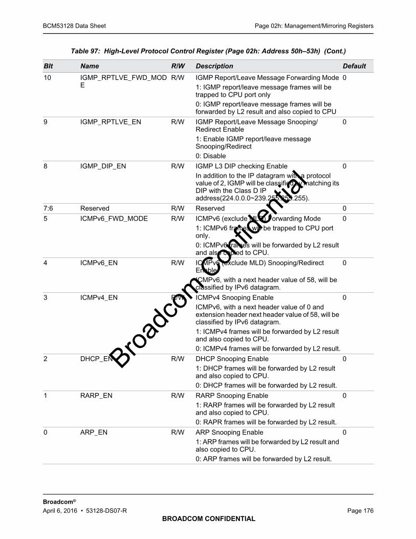
Page 02h: Management/Mirroring RegistersBCM53128 Data Sheet
BROADCOM CONFIDENTIAL
Broadcom®
April 6, 2016 • 53128-DS07-R Page 176
10 IGMP_RPTLVE_FWD_MODE
R/W IGMP Report/Leave Message Forwarding Mode1: IGMP report/leave message frames will betrapped to CPU port only0: IGMP report/leave message frames will beforwarded by L2 result and also copied to CPU
0
9 IGMP_RPTLVE_EN R/W IGMP Report/Leave Message Snooping/Redirect Enable1: Enable IGMP report/leave messageSnooping/Redirect0: Disable
0
8 IGMP_DIP_EN R/W IGMP L3 DIP checking EnableIn addition to the IP datagram with a protocolvalue of 2, IGMP will be classified by matching itsDIP with the Class D IPaddress(224.0.0.0~239.255.255.255).
0
7:6 Reserved R/W Reserved 0
5 ICMPv6_FWD_MODE R/W ICMPv6 (exclude MLD) Forwarding Mode1: ICMPv6 frames will be trapped to CPU portonly.0: ICMPv6 frames will be forwarded by L2 resultand also copied to CPU.
0
4 ICMPv6_EN R/W ICMPv6 (exclude MLD) Snooping/RedirectEnableICMPv6, with a next header value of 58, will beclassified by IPv6 datagram.
0
3 ICMPv4_EN R/W ICMPv4 Snooping EnableICMPv6, with a next header value of 0 andextension header next header value of 58, will beclassified by IPv6 datagram.1: ICMPv4 frames will be forwarded by L2 resultand also copied to CPU.0: ICMPv4 frames will be forwarded by L2 result.
0
2 DHCP_EN R/W DHCP Snooping Enable1: DHCP frames will be forwarded by L2 resultand also copied to CPU.0: DHCP frames will be forwarded by L2 result.
0
1 RARP_EN R/W RARP Snooping Enable1: RARP frames will be forwarded by L2 resultand also copied to CPU.0: RAPR frames will be forwarded by L2 result.
0
0 ARP_EN R/W ARP Snooping Enable1: ARP frames will be forwarded by L2 result andalso copied to CPU.0: ARP frames will be forwarded by L2 result.
0
Table 97: High-Level Protocol Control Register (Page 02h: Address 50h–53h) (Cont.)
BIt Name R/W Description Default
Broadc
om C
onfid
entia
l
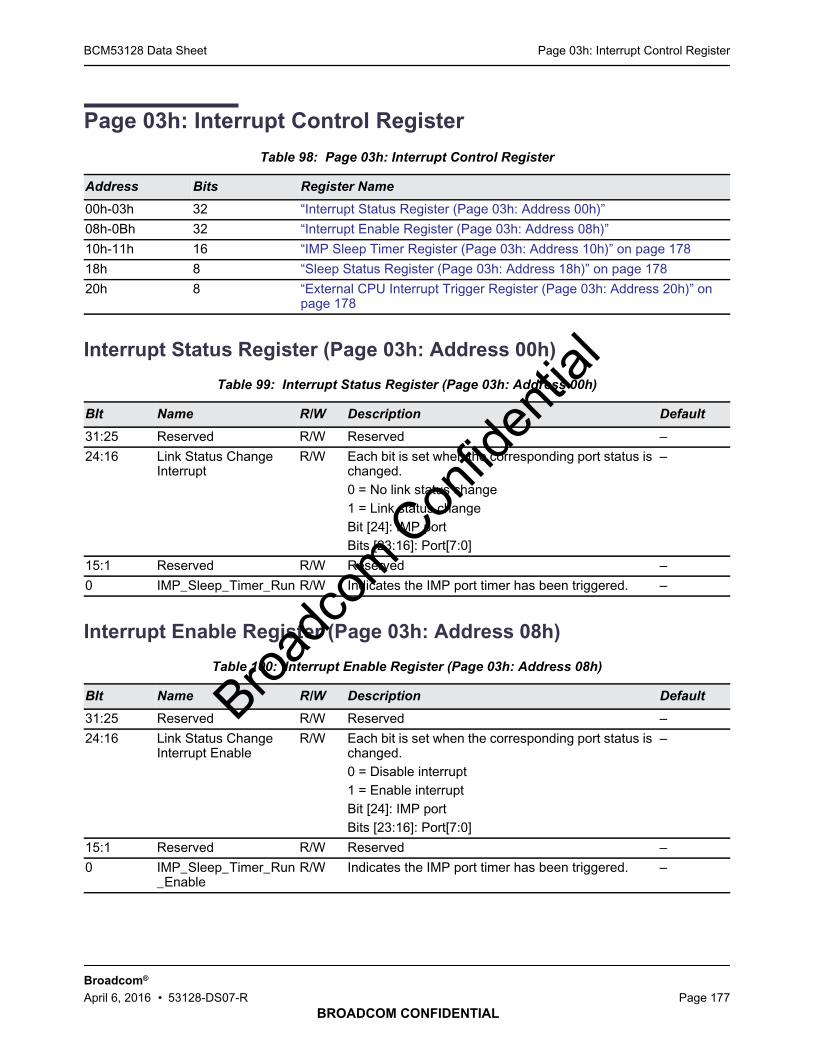
Page 03h: Interrupt Control RegisterBCM53128 Data Sheet
BROADCOM CONFIDENTIAL
Broadcom®
April 6, 2016 • 53128-DS07-R Page 177
Page 03h: Interrupt Control Register
Interrupt Status Register (Page 03h: Address 00h)
Interrupt Enable Register (Page 03h: Address 08h)
Table 98: Page 03h: Interrupt Control Register
Address Bits Register Name
00h-03h 32 “Interrupt Status Register (Page 03h: Address 00h)”
08h-0Bh 32 “Interrupt Enable Register (Page 03h: Address 08h)”
10h-11h 16 “IMP Sleep Timer Register (Page 03h: Address 10h)” on page 178
18h 8 “Sleep Status Register (Page 03h: Address 18h)” on page 178
20h 8 “External CPU Interrupt Trigger Register (Page 03h: Address 20h)” onpage 178
Table 99: Interrupt Status Register (Page 03h: Address 00h)
BIt Name R/W Description Default
31:25 Reserved R/W Reserved –
24:16 Link Status ChangeInterrupt
R/W Each bit is set when the corresponding port status ischanged.0 = No link status change1 = Link status changeBit [24]: IMP portBits [23:16]: Port[7:0]
–
15:1 Reserved R/W Reserved –
0 IMP_Sleep_Timer_Run R/W Indicates the IMP port timer has been triggered. –
Table 100: Interrupt Enable Register (Page 03h: Address 08h)
BIt Name R/W Description Default
31:25 Reserved R/W Reserved –
24:16 Link Status ChangeInterrupt Enable
R/W Each bit is set when the corresponding port status ischanged.0 = Disable interrupt1 = Enable interruptBit [24]: IMP portBits [23:16]: Port[7:0]
–
15:1 Reserved R/W Reserved –
0 IMP_Sleep_Timer_Run_Enable
R/W Indicates the IMP port timer has been triggered. –
Broadc
om C
onfid
entia
l
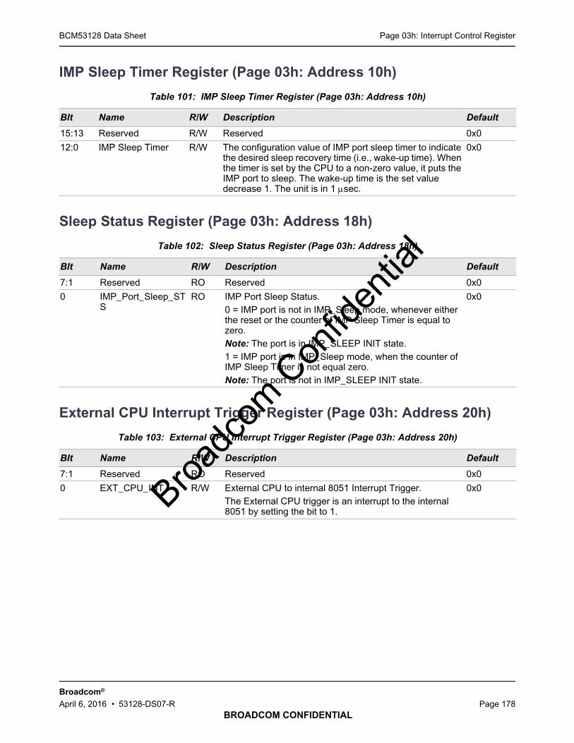
Page 03h: Interrupt Control RegisterBCM53128 Data Sheet
BROADCOM CONFIDENTIAL
Broadcom®
April 6, 2016 • 53128-DS07-R Page 178
IMP Sleep Timer Register (Page 03h: Address 10h)
Sleep Status Register (Page 03h: Address 18h)
External CPU Interrupt Trigger Register (Page 03h: Address 20h)
Table 101: IMP Sleep Timer Register (Page 03h: Address 10h)
BIt Name R/W Description Default
15:13 Reserved R/W Reserved 0x0
12:0 IMP Sleep Timer R/W The configuration value of IMP port sleep timer to indicatethe desired sleep recovery time (i.e., wake-up time). Whenthe timer is set by the CPU to a non-zero value, it puts theIMP port to sleep. The wake-up time is the set valuedecrease 1. The unit is in 1 sec.
0x0
Table 102: Sleep Status Register (Page 03h: Address 18h)
BIt Name R/W Description Default
7:1 Reserved RO Reserved 0x0
0 IMP_Port_Sleep_STS
RO IMP Port Sleep Status.0 = IMP port is not in IMP_Sleep mode, whenever eitherthe reset or the counter of IMP Sleep Timer is equal tozero.Note: The port is in IMP_SLEEP INIT state.1 = IMP port is in IMP_Sleep mode, when the counter ofIMP Sleep Timer is not equal zero.Note: The port is not in IMP_SLEEP INIT state.
0x0
Table 103: External CPU Interrupt Trigger Register (Page 03h: Address 20h)
BIt Name R/W Description Default
7:1 Reserved RO Reserved 0x0
0 EXT_CPU_INT R/W External CPU to internal 8051 Interrupt Trigger.The External CPU trigger is an interrupt to the internal8051 by setting the bit to 1.
0x0Broadc
om C
onfid
entia
l
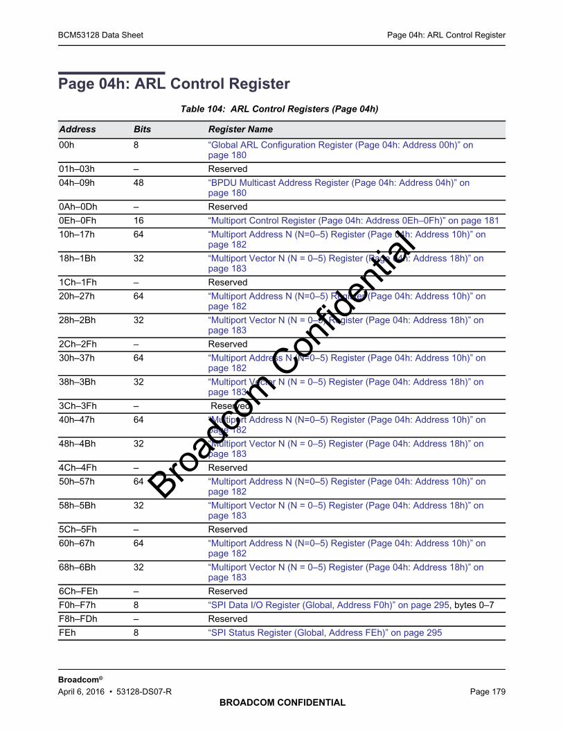
Page 04h: ARL Control RegisterBCM53128 Data Sheet
BROADCOM CONFIDENTIAL
Broadcom®
April 6, 2016 • 53128-DS07-R Page 179
Page 04h: ARL Control Register
Table 104: ARL Control Registers (Page 04h)
Address Bits Register Name
00h 8 “Global ARL Configuration Register (Page 04h: Address 00h)” onpage 180
01h–03h – Reserved
04h–09h 48 “BPDU Multicast Address Register (Page 04h: Address 04h)” onpage 180
0Ah–0Dh – Reserved
0Eh–0Fh 16 “Multiport Control Register (Page 04h: Address 0Eh–0Fh)” on page 181
10h–17h 64 “Multiport Address N (N=0–5) Register (Page 04h: Address 10h)” onpage 182
18h–1Bh 32 “Multiport Vector N (N = 0–5) Register (Page 04h: Address 18h)” onpage 183
1Ch–1Fh – Reserved
20h–27h 64 “Multiport Address N (N=0–5) Register (Page 04h: Address 10h)” onpage 182
28h–2Bh 32 “Multiport Vector N (N = 0–5) Register (Page 04h: Address 18h)” onpage 183
2Ch–2Fh – Reserved
30h–37h 64 “Multiport Address N (N=0–5) Register (Page 04h: Address 10h)” onpage 182
38h–3Bh 32 “Multiport Vector N (N = 0–5) Register (Page 04h: Address 18h)” onpage 183
3Ch–3Fh – Reserved
40h–47h 64 “Multiport Address N (N=0–5) Register (Page 04h: Address 10h)” onpage 182
48h–4Bh 32 “Multiport Vector N (N = 0–5) Register (Page 04h: Address 18h)” onpage 183
4Ch–4Fh – Reserved
50h–57h 64 “Multiport Address N (N=0–5) Register (Page 04h: Address 10h)” onpage 182
58h–5Bh 32 “Multiport Vector N (N = 0–5) Register (Page 04h: Address 18h)” onpage 183
5Ch–5Fh – Reserved
60h–67h 64 “Multiport Address N (N=0–5) Register (Page 04h: Address 10h)” onpage 182
68h–6Bh 32 “Multiport Vector N (N = 0–5) Register (Page 04h: Address 18h)” onpage 183
6Ch–FEh – Reserved
F0h–F7h 8 “SPI Data I/O Register (Global, Address F0h)” on page 295, bytes 0–7
F8h–FDh – Reserved
FEh 8 “SPI Status Register (Global, Address FEh)” on page 295
Broadc
om C
onfid
entia
l
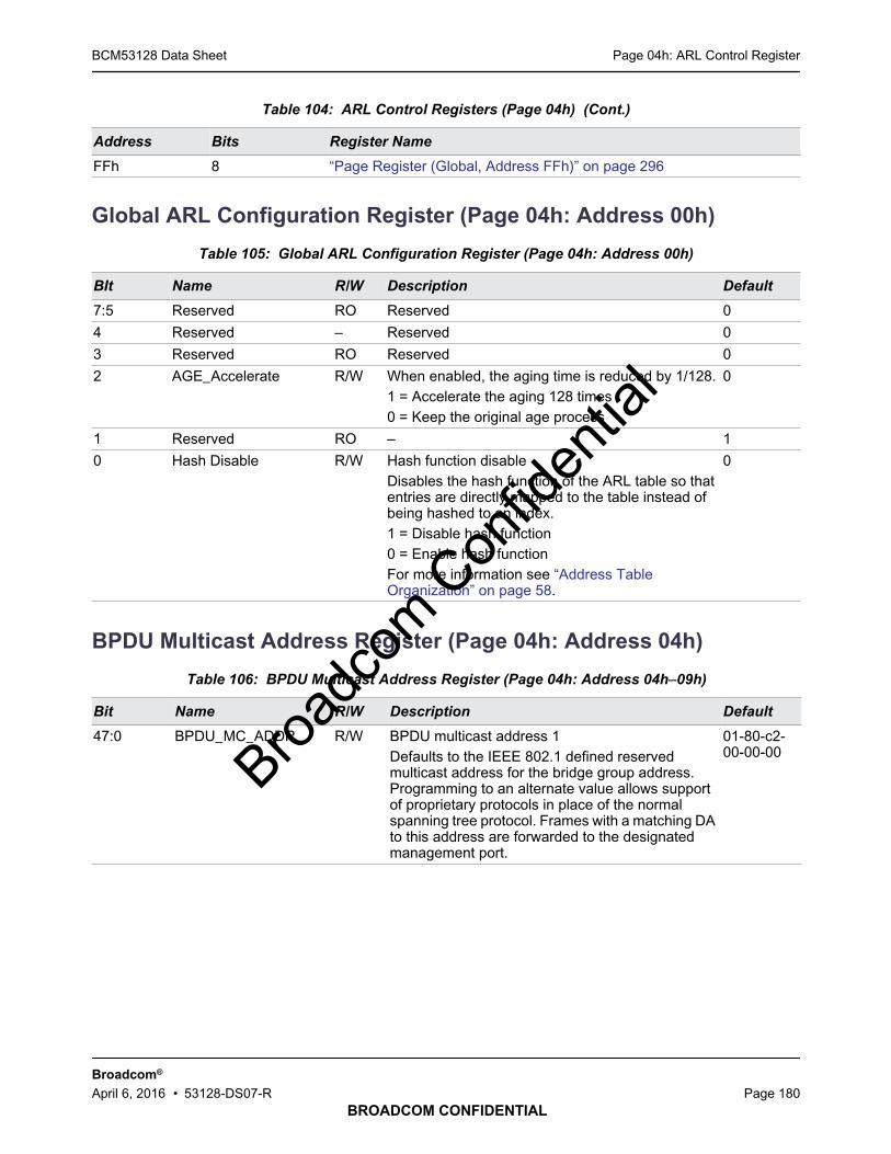
Page 04h: ARL Control RegisterBCM53128 Data Sheet
BROADCOM CONFIDENTIAL
Broadcom®
April 6, 2016 • 53128-DS07-R Page 180
Global ARL Configuration Register (Page 04h: Address 00h)
BPDU Multicast Address Register (Page 04h: Address 04h)
FFh 8 “Page Register (Global, Address FFh)” on page 296
Table 105: Global ARL Configuration Register (Page 04h: Address 00h)
BIt Name R/W Description Default
7:5 Reserved RO Reserved 0
4 Reserved – Reserved 0
3 Reserved RO Reserved 0
2 AGE_Accelerate R/W When enabled, the aging time is reduced by 1/128.1 = Accelerate the aging 128 times0 = Keep the original age process
0
1 Reserved RO – 1
0 Hash Disable R/W Hash function disableDisables the hash function of the ARL table so thatentries are directly mapped to the table instead ofbeing hashed to an index.1 = Disable hash function0 = Enable hash functionFor more information see “Address TableOrganization” on page 58.
0
Table 106: BPDU Multicast Address Register (Page 04h: Address 04h–09h)
Bit Name R/W Description Default
47:0 BPDU_MC_ADDR R/W BPDU multicast address 1Defaults to the IEEE 802.1 defined reservedmulticast address for the bridge group address.Programming to an alternate value allows supportof proprietary protocols in place of the normalspanning tree protocol. Frames with a matching DAto this address are forwarded to the designatedmanagement port.
01-80-c2-00-00-00
Table 104: ARL Control Registers (Page 04h) (Cont.)
Address Bits Register Name
Broadc
om C
onfid
entia
l

Page 04h: ARL Control RegisterBCM53128 Data Sheet
BROADCOM CONFIDENTIAL
Broadcom®
April 6, 2016 • 53128-DS07-R Page 181
Multiport Control Register (Page 04h: Address 0Eh–0Fh)
Table 107: Multiport Control Register (Page 04h: Address 0Eh–0Fh)
Bit Name R/W Description Default
15 MPORT0_TS-EN R/W Mport 0 Time Sync Enable1: Packet will be time-stamped if forwarded to CPU.MPORT_VECTOR0 should be programmed to CPUonly if this bit is set.0: Packet will not be time-stamped
0
14:12 Reserved RO Reserved 0
11:10 MPORT_CTRL5 R/W Multiport 5 Control00: Disable Multiport 5 Forward.10: Compare MPORT_ADD5 only; Forward basedon MPORT_Vector 5 if matched.01: Compare MPORT_ETYPE5 only; Forwardbased on MPORT_Vector 5 if matched.11: Compare MPORT_ETYPE5 andMPORT_ADD5; Forward based on MPORT_Vector5 if matched.
00
9:8 MPORT_CTRL4 R/W Multiport 4 Control00: Disable Multiport 4 Forward.10: Compare MPORT_ADD4 only; Forward basedon MPORT_Vector 4 if matched.01: Compare MPORT_ETYPE4 only; Forwardbased on MPORT_Vector 4 if matched.11: Compare MPORT_ETYPE4 andMPORT_ADD4; Forward based on MPORT_Vector4 if matched.
00
7:6 MPORT_CTRL3 R/W Multiport 3 Control00: Disable Multiport 3 Forward.10: Compare MPORT_ADD3 only; Forward basedon MPORT_Vector 3 if matched.01: Compare MPORT_ETYPE3 only; Forwardbased on MPORT_Vector 3 if matched.11: Compare MPORT_ETYPE3 andMPORT_ADD3; Forward based on MPORT_Vector3 if matched.
00
5:4 MPORT_CTRL2 R/W Multiport 2 Control00: Disable Multiport 2 Forward.10: Compare MPORT_ADD2 only; Forward basedon MPORT_Vector 2 if matched.01: Compare MPORT_ETYPE2 only; Forwardbased on MPORT_Vector 2 if matched.11: Compare MPORT_ETYPE2 andMPORT_ADD2; Forward based on MPORT_Vector2 if matched.
00
Broadc
om C
onfid
entia
l
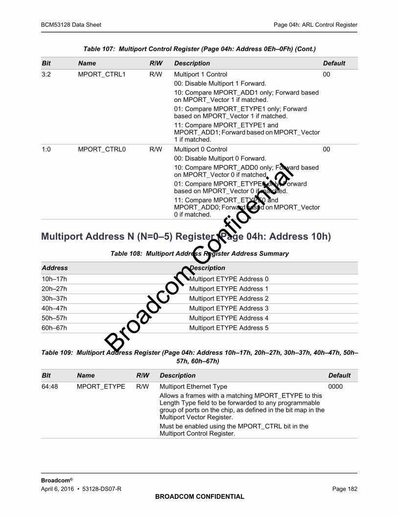
Page 04h: ARL Control RegisterBCM53128 Data Sheet
BROADCOM CONFIDENTIAL
Broadcom®
April 6, 2016 • 53128-DS07-R Page 182
Multiport Address N (N=0–5) Register (Page 04h: Address 10h).
3:2 MPORT_CTRL1 R/W Multiport 1 Control00: Disable Multiport 1 Forward.10: Compare MPORT_ADD1 only; Forward basedon MPORT_Vector 1 if matched.01: Compare MPORT_ETYPE1 only; Forwardbased on MPORT_Vector 1 if matched.11: Compare MPORT_ETYPE1 andMPORT_ADD1; Forward based on MPORT_Vector1 if matched.
00
1:0 MPORT_CTRL0 R/W Multiport 0 Control00: Disable Multiport 0 Forward.10: Compare MPORT_ADD0 only; Forward basedon MPORT_Vector 0 if matched.01: Compare MPORT_ETYPE0 only; Forwardbased on MPORT_Vector 0 if matched.11: Compare MPORT_ETYPE0 andMPORT_ADD0; Forward based on MPORT_Vector0 if matched.
00
Table 108: Multiport Address Register Address Summary
Address Description
10h–17h Multiport ETYPE Address 0
20h–27h Multiport ETYPE Address 1
30h–37h Multiport ETYPE Address 2
40h–47h Multiport ETYPE Address 3
50h–57h Multiport ETYPE Address 4
60h–67h Multiport ETYPE Address 5
Table 109: Multiport Address Register (Page 04h: Address 10h–17h, 20h–27h, 30h–37h, 40h–47h, 50h–57h, 60h–67h)
BIt Name R/W Description Default
64:48 MPORT_ETYPE R/W Multiport Ethernet TypeAllows a frames with a matching MPORT_ETYPE to thisLength Type field to be forwarded to any programmablegroup of ports on the chip, as defined in the bit map in theMultiport Vector Register.Must be enabled using the MPORT_CTRL bit in theMultiport Control Register.
0000
Table 107: Multiport Control Register (Page 04h: Address 0Eh–0Fh) (Cont.)
Bit Name R/W Description Default
Broadc
om C
onfid
entia
l

Page 04h: ARL Control RegisterBCM53128 Data Sheet
BROADCOM CONFIDENTIAL
Broadcom®
April 6, 2016 • 53128-DS07-R Page 183
Multiport Vector N (N = 0–5) Register (Page 04h: Address 18h).
47:0 MPORT_ADDR R/W Multiport AddressAllows a frames with a matching DA to this address to beforwarded to any programmable group of ports on the chip,as defined in the bit map in the Multiport Vector Register.Must be enabled using the MPORT_CTRL bit in theMultiport Control Register.
000000000000
Table 110: Multiport Vector Register Address Summary
Address Description
18h–1Bh Multiport Vector 0
28h–2Bh Multiport Vector 1
38h–3Bh Multiport Vector 2
48h–4Bh Multiport Vector 3
58h–5Bh Multiport Vector 4
68h–6Bh Multiport Vector 5
Table 111: Multiport Vector Register (Page 04h: Address 18h–1Bh, 28h–2Bh, 38h–3Bh, 48h–4Bh, 58h–5Bh, 68h–6Bh)
BIt Name R/W Description Default
31:9 Reserved R/O Reserved 0
8:0 MPORT_VCTR_N R/W Multiport VectorA bit mask corresponding to the physical ports onthe chip.A frame with a DA matching the content of theMultiport Address Register will be forwarded toeach port with a bit set in the Multiport Vector bitmap.Bits[7:0] correspond to ports[7:0]Bit 8: Management Port (MII Management)
0
Table 109: Multiport Address Register (Page 04h: Address 10h–17h, 20h–27h, 30h–37h, 40h–47h, 50h–57h, 60h–67h) (Cont.)
BIt Name R/W Description Default
Broadc
om C
onfid
entia
l
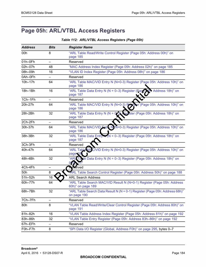
Page 05h: ARL/VTBL Access RegistersBCM53128 Data Sheet
BROADCOM CONFIDENTIAL
Broadcom®
April 6, 2016 • 53128-DS07-R Page 184
Page 05h: ARL/VTBL Access Registers
Table 112: ARL/VTBL Access Registers (Page 05h)
Address Bits Register Name
00h 8 “ARL Table Read/Write Control Register (Page 05h: Address 00h)” onpage 185
01h–0Fh – Reserved
02h–07h 48 “MAC Address Index Register (Page 05h: Address 02h)” on page 185
08h–09h 16 “VLAN ID Index Register (Page 05h: Address 08h)” on page 186
0Ah–0Fh – Reserved
10h–17h 64 “ARL Table MAC/VID Entry N (N=0-3) Register (Page 05h: Address 10h)” onpage 186
18h–1Bh 16 “ARL Table Data Entry N (N = 0–3) Register (Page 05h: Address 18h)” onpage 187
1Ch–1Fh – Reserved
20h-27h 64 “ARL Table MAC/VID Entry N (N=0-3) Register (Page 05h: Address 10h)” onpage 186
28h-2Bh 32 “ARL Table Data Entry N (N = 0–3) Register (Page 05h: Address 18h)” onpage 187
2Ch-2Fh – Reserved
30h-37h 64 “ARL Table MAC/VID Entry N (N=0-3) Register (Page 05h: Address 10h)” onpage 186
38h-3Bh 32 “ARL Table Data Entry N (N = 0–3) Register (Page 05h: Address 18h)” onpage 187
3Ch-3Fh – Reserved
40h-47h 64 “ARL Table MAC/VID Entry N (N=0-3) Register (Page 05h: Address 10h)” onpage 186
48h-4Bh 32 “ARL Table Data Entry N (N = 0–3) Register (Page 05h: Address 18h)” onpage 187
4Ch-4Fh – Reserved
50h 8 “ARL Table Search Control Register (Page 05h: Address 50h)” on page 188
51h–52h 16 ARL Search Address
60h–77h 64 “ARL Table Search MAC/VID Result N (N=0-1) Register (Page 05h: Address60h)” on page 189
68h–7Bh 32 “ARL Table Search Data Result N (N = 0-1) Register (Page 05h: Address 68h)”on page 190
7Ch–7Fh – Reserved
80h 8 “VLAN Table Read/Write/Clear Control Register (Page 05h: Address 80h)” onpage 191
81h–82h 16 “VLAN Table Address Index Register (Page 05h: Address 81h)” on page 192
83h–86h 32 “VLAN Table Entry Register (Page 05h: Address 83h–86h)” on page 192
67h–EFh – Reserved
F0h–F7h 8 “SPI Data I/O Register (Global, Address F0h)” on page 295, bytes 0–7
Broadc
om C
onfid
entia
l
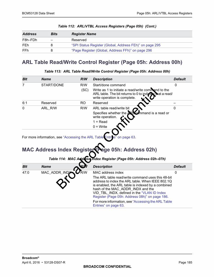
Page 05h: ARL/VTBL Access RegistersBCM53128 Data Sheet
BROADCOM CONFIDENTIAL
Broadcom®
April 6, 2016 • 53128-DS07-R Page 185
ARL Table Read/Write Control Register (Page 05h: Address 00h)
For more information, see “Accessing the ARL Table Entries” on page 63.
MAC Address Index Register (Page 05h: Address 02h)
F8h–FDh – Reserved
FEh 8 “SPI Status Register (Global, Address FEh)” on page 295
FFh 8 “Page Register (Global, Address FFh)” on page 296
Table 113: ARL Table Read/Write Control Register (Page 05h: Address 00h)
BIt Name R/W Description Default
7 START/DONE R/W(SC)
Start/done commandWrite as 1 to initiate a read/write command to theARL table. The bit returns to 0 to indicate that a read/write operation is complete.
0
6:1 Reserved RO Reserved –
0 ARL_R/W R/W ARL table read/write bitSpecifies whether the ARL command is a read orwrite operation.1 = Read0 = Write
0
Table 114: MAC Address Index Register (Page 05h: Address 02h–07h)
BIt Name R/W Description Default
47:0 MAC_ADDR_INDX R/W MAC address indexThe ARL table read/write command uses this 48-bitaddress to index the ARL table. When IEEE 802.1Qis enabled, the ARL table is indexed by a combinedhash of the MAC_ADDR_INDX and theVID_TBL_INDX, defined in the “VLAN ID IndexRegister (Page 05h: Address 08h)” on page 186.For more information, see “Accessing the ARL TableEntries” on page 63.
0
Table 112: ARL/VTBL Access Registers (Page 05h) (Cont.)
Address Bits Register Name
Broadc
om C
onfid
entia
l

Page 05h: ARL/VTBL Access RegistersBCM53128 Data Sheet
BROADCOM CONFIDENTIAL
Broadcom®
April 6, 2016 • 53128-DS07-R Page 186
VLAN ID Index Register (Page 05h: Address 08h)
ARL Table MAC/VID Entry N (N=0-3) Register (Page 05h: Address10h)
.
Table 115: VLAN ID Index Register (Page 05h: Address 08h–09h)
BIt Name R/W Description Default
15:12 Reserved R/W Reserved 0
11:0 VID_INDX R/W VLAN ID indexWhen IEEE 802.1Q is enabled, the VLAN ID Indexis used with the MAC_ADDR_INDX, defined in the“MAC Address Index Register (Page 05h: Address02h)” on page 185, to form the hash index forwhich status is to be read or written.For more information, see “Accessing the ARLTable Entries” on page 63.
0
Table 116: ARL Table MAC/VID Entry N (N=0-3) Register Address Summary
Address Description
10h–17h ARL Table MAC/VID Entry 0
20h–27h ARL Table MAC/VID Entry 1
30h–37h ARL Table MAC/VID Entry 2
40h–47h ARL Table MAC/VID Entry 3
Table 117: ARL Table MAC/VID Entry N (N=0-3) Register (Page 05h: Address 10h–17h, 20h–27h, 30h–37h, 40h–47h)
BIt Name R/W Description Default
63:60 Reserved R/O Reserved 0
59:48 VID_N R/W VID entry NThe VID field is either read from or written to theARL table entry N.The VID is a “don’t-care” field when IEEE 802.1Qis disabled.
0
47:0 MACADDR_N R/W MAC address entry NThe 48-bit MAC Address field to be either readfrom or written to the ARL table entry N.
0
Note: Together, the “ARL Table MAC/VID Entry N (N=0-3) Register (Page 05h: Address 10h)” onpage 186 and the “ARL Table Data Entry N (N = 0–3) Register (Page 05h: Address 18h)” on page 187compose a complete entry in the ARL table. For more information, see “Accessing the ARL Table Entries”on page 63.
Broadc
om C
onfid
entia
l
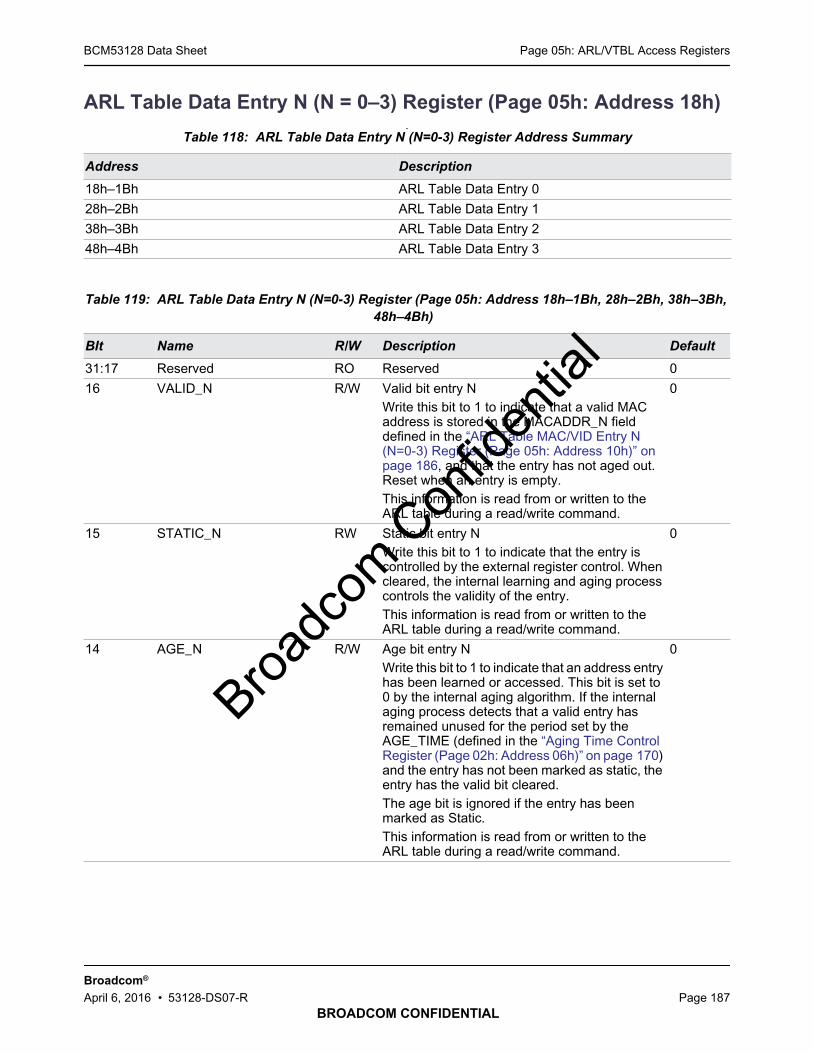
Page 05h: ARL/VTBL Access RegistersBCM53128 Data Sheet
BROADCOM CONFIDENTIAL
Broadcom®
April 6, 2016 • 53128-DS07-R Page 187
ARL Table Data Entry N (N = 0–3) Register (Page 05h: Address 18h).
Table 118: ARL Table Data Entry N (N=0-3) Register Address Summary
Address Description
18h–1Bh ARL Table Data Entry 0
28h–2Bh ARL Table Data Entry 1
38h–3Bh ARL Table Data Entry 2
48h–4Bh ARL Table Data Entry 3
Table 119: ARL Table Data Entry N (N=0-3) Register (Page 05h: Address 18h–1Bh, 28h–2Bh, 38h–3Bh,48h–4Bh)
BIt Name R/W Description Default
31:17 Reserved RO Reserved 0
16 VALID_N R/W Valid bit entry NWrite this bit to 1 to indicate that a valid MACaddress is stored in the MACADDR_N fielddefined in the “ARL Table MAC/VID Entry N(N=0-3) Register (Page 05h: Address 10h)” onpage 186, and that the entry has not aged out.Reset when an entry is empty.This information is read from or written to theARL table during a read/write command.
0
15 STATIC_N RW Static bit entry NWrite this bit to 1 to indicate that the entry iscontrolled by the external register control. Whencleared, the internal learning and aging processcontrols the validity of the entry.This information is read from or written to theARL table during a read/write command.
0
14 AGE_N R/W Age bit entry NWrite this bit to 1 to indicate that an address entryhas been learned or accessed. This bit is set to0 by the internal aging algorithm. If the internalaging process detects that a valid entry hasremained unused for the period set by theAGE_TIME (defined in the “Aging Time ControlRegister (Page 02h: Address 06h)” on page 170)and the entry has not been marked as static, theentry has the valid bit cleared.The age bit is ignored if the entry has beenmarked as Static.This information is read from or written to theARL table during a read/write command.
0
Broadc
om C
onfid
entia
l
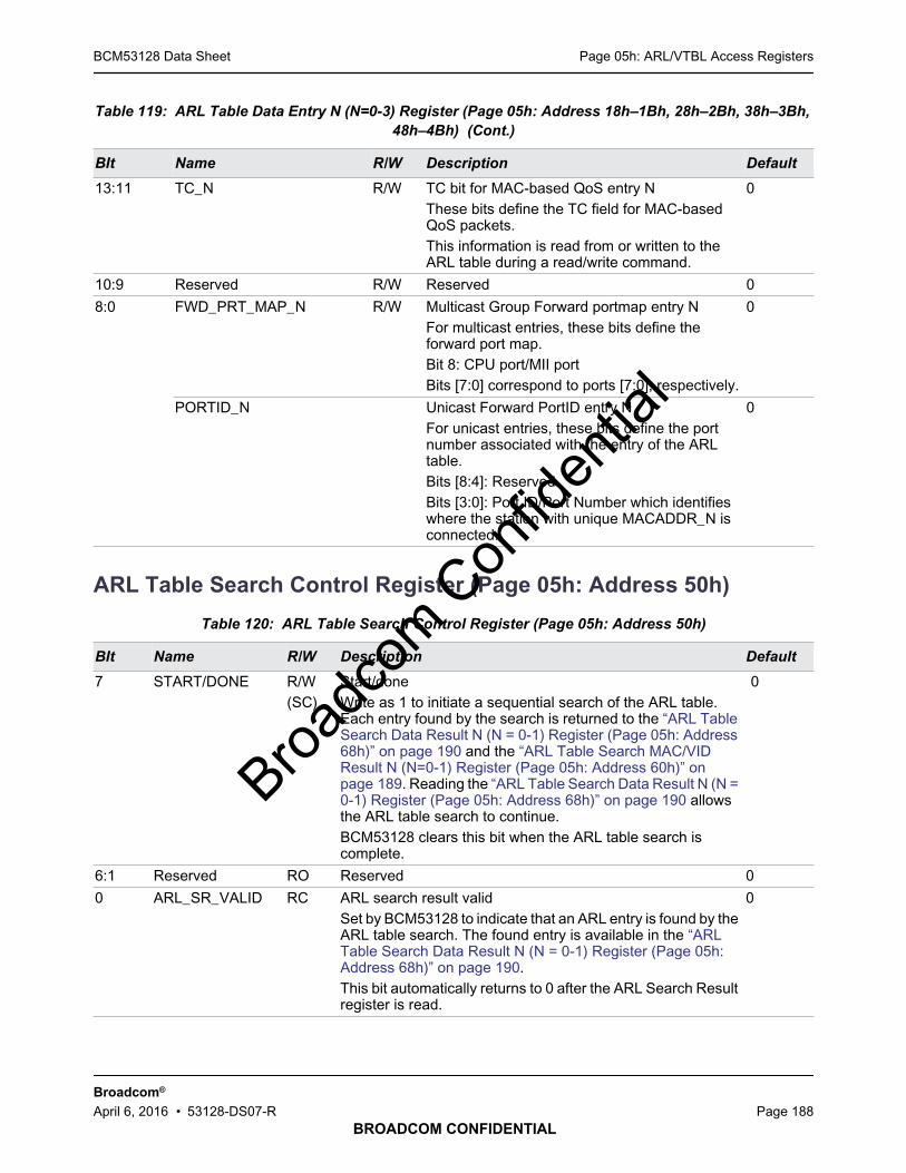
Page 05h: ARL/VTBL Access RegistersBCM53128 Data Sheet
BROADCOM CONFIDENTIAL
Broadcom®
April 6, 2016 • 53128-DS07-R Page 188
ARL Table Search Control Register (Page 05h: Address 50h)
13:11 TC_N R/W TC bit for MAC-based QoS entry NThese bits define the TC field for MAC-basedQoS packets.This information is read from or written to theARL table during a read/write command.
0
10:9 Reserved R/W Reserved 0
8:0 FWD_PRT_MAP_N R/W Multicast Group Forward portmap entry NFor multicast entries, these bits define theforward port map.Bit 8: CPU port/MII portBits [7:0] correspond to ports [7:0], respectively.
0
PORTID_N Unicast Forward PortID entry NFor unicast entries, these bits define the portnumber associated with the entry of the ARLtable.Bits [8:4]: ReservedBits [3:0]: Port ID/Port Number which identifieswhere the station with unique MACADDR_N isconnected.
0
Table 120: ARL Table Search Control Register (Page 05h: Address 50h)
BIt Name R/W Description Default
7 START/DONE R/W(SC)
Start/doneWrite as 1 to initiate a sequential search of the ARL table.Each entry found by the search is returned to the “ARL TableSearch Data Result N (N = 0-1) Register (Page 05h: Address68h)” on page 190 and the “ARL Table Search MAC/VIDResult N (N=0-1) Register (Page 05h: Address 60h)” onpage 189. Reading the “ARL Table Search Data Result N (N =0-1) Register (Page 05h: Address 68h)” on page 190 allowsthe ARL table search to continue.BCM53128 clears this bit when the ARL table search iscomplete.
0
6:1 Reserved RO Reserved 0
0 ARL_SR_VALID RC ARL search result validSet by BCM53128 to indicate that an ARL entry is found by theARL table search. The found entry is available in the “ARLTable Search Data Result N (N = 0-1) Register (Page 05h:Address 68h)” on page 190.This bit automatically returns to 0 after the ARL Search Resultregister is read.
0
Table 119: ARL Table Data Entry N (N=0-3) Register (Page 05h: Address 18h–1Bh, 28h–2Bh, 38h–3Bh,48h–4Bh) (Cont.)
BIt Name R/W Description Default
Broadc
om C
onfid
entia
l

Page 05h: ARL/VTBL Access RegistersBCM53128 Data Sheet
BROADCOM CONFIDENTIAL
Broadcom®
April 6, 2016 • 53128-DS07-R Page 189
For more information, see “Accessing the ARL Table Entries” on page 63.
ARL Search Address Register (Page 05h: Address 51h)
ARL Table Search MAC/VID Result N (N=0-1) Register (Page 05h:Address 60h)
.
For more information, see “Accessing the ARL Table Entries” on page 63.
Table 121: ARL Search Address Register (Page 05h: Address 51h–52h)
Bit Name R/W Description Default
15 ARL_ADDR_VALID
RO ARL address validIndicates the lower 15 bits of this register contain a validinternal representation of the ARL entry that is currentlybeing accessed. Intended for factory test/diagnostic useonly.
0
14:0 ARL_ADDR RO ARL address14-bit internal representation of the address of the ARLentry currently being accessed by the ARL search routine.This is not a direct address of the ARL location and isintended for factory test/diagnostic use only.
0
Table 122: ARL Table Search MAC/VID Result N (N=0-1) Register Address Summary
Address Description
60h–67h ARL Table Search MAC/VID Result 0
70h–77h ARL Table Search MAC/VID Result 1
Table 123: ARL Table Search MAC/VID Result N (N=0-1) Register (Page 05h: Address 60h–67h, 70h–77h)
BIt Name R/W Description Default
63:60 Reserved RO Reserved 0
59:48 ARL_SR_VID_N RO ARL search VID resultThese bits store the VID of the ARL table entryfound by the ARL table search function.
0
47:0 ARL_SR_MAC_N RO ARL search MAC address result.These bits store the MAC address of the ARLtable entry found by the ARL table searchfunction.
0Broa
dcom
Con
fiden
tial

Page 05h: ARL/VTBL Access RegistersBCM53128 Data Sheet
BROADCOM CONFIDENTIAL
Broadcom®
April 6, 2016 • 53128-DS07-R Page 190
ARL Table Search Data Result N (N = 0-1) Register (Page 05h:Address 68h)
Table 124: ARL Table Search Data Result N (N=0-1) Register Address Summary
Address Description
68h–6Bh ARL Table Search Data Result 0
78h–7Bh ARL Table Search Data Result 1
Table 125: ARL Table Search Data Result N (N=0-1) Register (Page 05h: Address 68h–6Bh, 78h–7Bh)
BIt Name R/W Description Default
31:17 Reserved RO Reserved 0
16 ARL_SR_VALID_N RO ARL search valid bit result.This bit stores the valid bit of the ARL table entryfound by the ARL table search function. Readingthis register clears the data from the register andallows the ARL table search function to continuesearching.
0
15 ARL_SR_STATIC_N RO ARL search static bit result.This bit stores the static bit of the ARL table entryfound by the ARL table search function. Readingthis register clears the data from the register andallows the ARL table search function to continuesearching.
0
14 ARL_SR_AGE_N RO ARL search age bit result.This bit stores the Age bit of the ARL table entryfound by the ARL table search function. Readingthis register clears the data from the register andallows the ARL table search function to continuesearching.
0
13:11 ARL_SR_TC_N RO ARL search TC bits result.These bits store the TC bits of the ARL tableentry found by the ARL table search function.Reading this register clears the data from theregister and allows the ARL table search functionto continue searching.
0
10:9 Reserved RO Reserved 0
Broadc
om C
onfid
entia
l
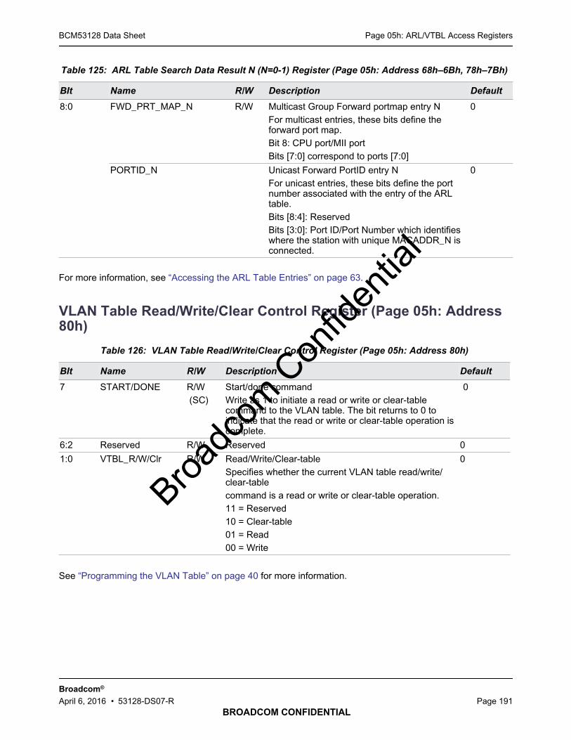
Page 05h: ARL/VTBL Access RegistersBCM53128 Data Sheet
BROADCOM CONFIDENTIAL
Broadcom®
April 6, 2016 • 53128-DS07-R Page 191
For more information, see “Accessing the ARL Table Entries” on page 63.
VLAN Table Read/Write/Clear Control Register (Page 05h: Address80h)
See “Programming the VLAN Table” on page 40 for more information.
8:0 FWD_PRT_MAP_N R/W Multicast Group Forward portmap entry NFor multicast entries, these bits define theforward port map.Bit 8: CPU port/MII portBits [7:0] correspond to ports [7:0]
0
PORTID_N Unicast Forward PortID entry NFor unicast entries, these bits define the portnumber associated with the entry of the ARLtable.Bits [8:4]: ReservedBits [3:0]: Port ID/Port Number which identifieswhere the station with unique MACADDR_N isconnected.
0
Table 126: VLAN Table Read/Write/Clear Control Register (Page 05h: Address 80h)
BIt Name R/W Description Default
7 START/DONE R/W(SC)
Start/done commandWrite as 1 to initiate a read or write or clear-tablecommand to the VLAN table. The bit returns to 0 toindicate that the read or write or clear-table operation iscomplete.
0
6:2 Reserved R/W Reserved 0
1:0 VTBL_R/W/Clr R/W Read/Write/Clear-tableSpecifies whether the current VLAN table read/write/clear-tablecommand is a read or write or clear-table operation.11 = Reserved10 = Clear-table01 = Read00 = Write
0
Table 125: ARL Table Search Data Result N (N=0-1) Register (Page 05h: Address 68h–6Bh, 78h–7Bh)
BIt Name R/W Description Default
Broadc
om C
onfid
entia
l
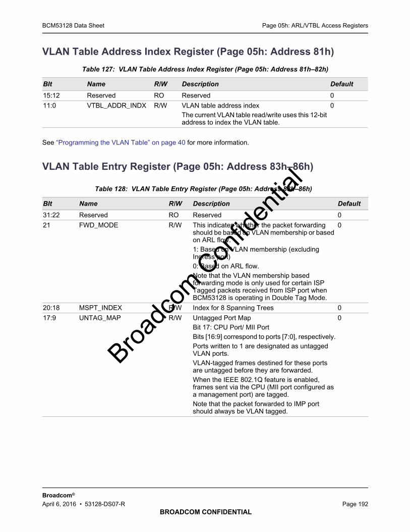
Page 05h: ARL/VTBL Access RegistersBCM53128 Data Sheet
BROADCOM CONFIDENTIAL
Broadcom®
April 6, 2016 • 53128-DS07-R Page 192
VLAN Table Address Index Register (Page 05h: Address 81h)
See “Programming the VLAN Table” on page 40 for more information.
VLAN Table Entry Register (Page 05h: Address 83h–86h)
Table 127: VLAN Table Address Index Register (Page 05h: Address 81h–82h)
BIt Name R/W Description Default
15:12 Reserved RO Reserved 0
11:0 VTBL_ADDR_INDX R/W VLAN table address indexThe current VLAN table read/write uses this 12-bitaddress to index the VLAN table.
0
Table 128: VLAN Table Entry Register (Page 05h: Address 83h–86h)
BIt Name R/W Description Default
31:22 Reserved RO Reserved 0
21 FWD_MODE R/W This indicates whether the packet forwardingshould be based on VLAN membership or basedon ARL flow.1: Based on VLAN membership (excludingIngress port)0: Based on ARL flow.Note that the VLAN membership basedforwarding mode is only used for certain ISPTagged packets received from ISP port whenBCM53128 is operating in Double Tag Mode.
0
20:18 MSPT_INDEX R/W Index for 8 Spanning Trees 0
17:9 UNTAG_MAP R/W Untagged Port MapBit 17: CPU Port/ MII PortBits [16:9] correspond to ports [7:0], respectively.Ports written to 1 are designated as untaggedVLAN ports.VLAN-tagged frames destined for these portsare untagged before they are forwarded.When the IEEE 802.1Q feature is enabled,frames sent via the CPU (MII port configured asa management port) are tagged.Note that the packet forwarded to IMP portshould always be VLAN tagged.
0
Broadc
om C
onfid
entia
l

Page 05h: ARL/VTBL Access RegistersBCM53128 Data Sheet
BROADCOM CONFIDENTIAL
Broadcom®
April 6, 2016 • 53128-DS07-R Page 193
See “Programming the VLAN Table” on page 40 for more information.
8:0 FWD_MAP R/W Forward Port MapThe VLAN-tagged Frame is allowed to beforwarded to the destination ports correspondingbits set in the Map Ports written to 1 aredesignated as capable of receiving VLAN-taggedframes.Bit 8: CPU Port/ MII PortBits [7:0] correspond to Ports [7:0], respectively.
0
Table 128: VLAN Table Entry Register (Page 05h: Address 83h–86h) (Cont.)
BIt Name R/W Description Default
Broadc
om C
onfid
entia
l

Page 10h–17h: Internal GPHY MII RegistersBCM53128 Data Sheet
BROADCOM CONFIDENTIAL
Broadcom®
April 6, 2016 • 53128-DS07-R Page 194
Page 10h–17h: Internal GPHY MII Registers
Table 129: 10/100/1000 PHY Page Summary
Page Description
10h Port 0 Internal PHY MII Registers
11h Port 1 Internal PHY MII Registers
12h Port 2 Internal PHY MII Registers
13h Port 3 Internal PHY MII Registers
14h Port 4 Internal PHY MII Registers
15h Port 5 Internal PHY MII Registers
16h Port 6 Internal PHY MII Registers
17h Port 7 Internal PHY MII Registers
Table 130: Register Map (Page 10h–17h)
SPI OffsetAddress
MIIAddress
Numberof Bits Register Table
10BASE-T/100BASE-TX/1000BASE-T Registers
00h 00h 16 Table 131: “MII Control Register (Page 10h–17h: Address 00h–01h),” onpage 196
02h 01h 16 Table 132: “MII Status Register (Page 10h–17h: Address 02h–03h),” onpage 197
04h–06h 02h 32 Table 133: “PHY Identifier Register MSB (Page 10h–17h: Address 04–07h),”on page 198
08h 04h 16 Table 135: “Auto-Negotiation Advertisement Register (Page 10h–17h:Address 08h–09h),” on page 199
0Ah 05h 16 Table 136: “Auto-Negotiation Link Partner Ability Register (Page 10h–17h:Address 0Ah–0Bh),” on page 200
0Ch 06h 16 Table 136: “Auto-Negotiation Link Partner Ability Register (Page 10h–17h:Address 0Ah–0Bh),” on page 200
0Eh 07h 16 Table 138: “Next Page Transmit Register (Page 10h–17h: Address 0Eh–0Fh),”on page 202
10h 08h 16 Table 139: “Link Partner Received Next Page Register (Page 10h–17h:Address 10h–11h),” on page 203
12h 09h 16 Table 140: “1000BASE-T Control Register (Page 10h–17h: Address 12h–13h),” on page 204
14h 0Ah 16 Table 141: “1000BASE-T Status Register (Page 10h–17h: Address 14h–15h),”on page 205
16h–1Dh – 16 Reserved (Do not read from or write to a reserved register.)
1Eh 0Fh 16 Table 142: “IEEE Extended Status Register (Page 10h–17h: Address 1Eh–1Fh),” on page 206
20h 10h 16 Table 143: “PHY Extended Control Register (Page 10h–17h: Address 20h–21h),” on page 207
Broadc
om C
onfid
entia
l
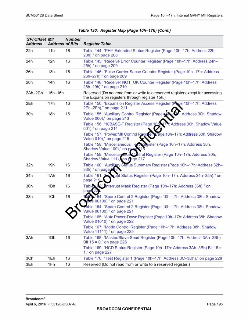
Page 10h–17h: Internal GPHY MII RegistersBCM53128 Data Sheet
BROADCOM CONFIDENTIAL
Broadcom®
April 6, 2016 • 53128-DS07-R Page 195
22h 11h 16 Table 144: “PHY Extended Status Register (Page 10h–17h: Address 22h–23h),” on page 208
24h 12h 16 Table 145: “Receive Error Counter Register (Page 10h–17h: Address 24h–25h),” on page 209
26h 13h 16 Table 146: “False Carrier Sense Counter Register (Page 10h–17h: Address26h–27h),” on page 209
28h 14h 16 Table 148: “Receiver NOT_OK Counter Register (Page 10h–17h: Address28h–29h),” on page 210
2Ah–2Ch 15h–16h Reserved (Do not read from or write to a reserved register except for accessingthe Expansion registers through register 15h.)
2Eh 17h 16 Table 150: “Expansion Register Access Register (Page 10h–17h: Address2Eh–2Fh),” on page 211
30h 18h 16 Table 155: “Auxiliary Control Register (Page 10h–17h: Address 30h, ShadowValue 000),” on page 213Table 156: “10BASE-T Register (Page 10h–17h: Address 30h, Shadow Value001),” on page 214Table 157: “Power/MII Control Register (Page 10h–17h: Address 30h, ShadowValue 010),” on page 215Table 158: “Miscellaneous Test Register (Page 10h–17h: Address 30h,Shadow Value 100),” on page 216Table 159: “Miscellaneous Control Register (Page 10h–17h: Address 30h,Shadow Value 111),” on page 217
32h 19h 16 Table 160: “Auxiliary Status Summary Register (Page 10h–17h: Address 32h–33h),” on page 218
34h 1Ah 16 Table 161: “Interrupt Status Register (Page 10h–17h: Address 34h–35h),” onpage 219
36h 1Bh 16 Table 162: “Interrupt Mask Register (Page 10h–17h: Address 36h),” onpage 220
38h 1Ch 16 Table 164: “Spare Control 2 Register (Page 10h–17h: Address 38h, ShadowValue 00100),” on page 221Table 164: “Spare Control 2 Register (Page 10h–17h: Address 38h, ShadowValue 00100),” on page 221Table 165: “Auto Power-Down Register (Page 10h–17h: Address 38h, ShadowValue 01010),” on page 222Table 167: “Mode Control Register (Page 10h–17h: Address 38h, ShadowValue 11111),” on page 225
3Ah 1Dh 16 Table 168: “Master/Slave Seed Register (Page 10h–17h: Address 3Ah–3Bh)Bit 15 = 0,” on page 226Table 169: “HCD Status Register (Page 10h–17h: Address 3Ah–3Bh) Bit 15 =1,” on page 227
3Ch 1Eh 16 Table 170: “Test Register 1 (Page 10h–17h: Address 3C–3Dh),” on page 228
3Eh 1Fh 16 Reserved (Do not read from or write to a reserved register.)
Table 130: Register Map (Page 10h–17h) (Cont.)
SPI OffsetAddress
MIIAddress
Numberof Bits Register Table
Broadc
om C
onfid
entia
l

Page 10h–17h: Internal GPHY MII RegistersBCM53128 Data Sheet
BROADCOM CONFIDENTIAL
Broadcom®
April 6, 2016 • 53128-DS07-R Page 196
MII Control Register (Page 10h–17h: Address 00h–01h)
Expansion Registers: Read/Write through Register 2Ah (Accessed by Writing to Register 2Eh, Bits[11:0] = 1111 + Expansion Register Number)
00h – – Table 171: “Expansion Register 00h: Receive/Transmit Packet Counter,” onpage 229
01h – – Table 172: “Expansion Register 01h: Expansion Interrupt Status,” on page 229
04h – – –
05h – – –
07h – – –
45h – – Table 173: “Expansion Register 45h: Transmit CRC,” on page 230
Table 131: MII Control Register (Page 10h–17h: Address 00h–01h)
Bit Name R/W Description Default
15 Reset R/WSC
1 = PHY reset0 = Normal operation
0
14 Internal Loopback R/W 1 = Loopback mode0 = Normal operation
0
13 Speed Selection (LSB) R/W Bits [6,13]:11 = Reserved10 = 1000 Mbps01 = 100 Mbps00 = 10 Mbps
0
12 Auto-negotiation Enable R/W 1 = Auto-negotiation is enabled.0 = Auto-negotiation is disabled.
1
11 Power Down R/W 1 = Power-down0 = Normal operation
0
10 Isolate R/W 1 = Electrically isolate PHY from GMII.0 = Normal operation
0
9 Restart Auto-negotiation R/WSC
1 = Restarting auto-negotiation0 = Auto-negotiation restart is complete.
0
8 Duplex Mode R/W 1 = Full-duplex0 = Half-duplex
1
7 Collision Test Enable R/W 1 = Enable the collision test mode.0 = Disable the collision test mode.
0
6 Speed Selection (MSB) R/W Works in conjunction with bit 13 1
5 Reserved R/W Write as 0, ignore on read. 0
4 Reserved R/W Write as 0 ignore on read 0
3 Reserved R/W Write as 0 ignore on read 0
Table 130: Register Map (Page 10h–17h) (Cont.)
SPI OffsetAddress
MIIAddress
Numberof Bits Register Table
Broadc
om C
onfid
entia
l
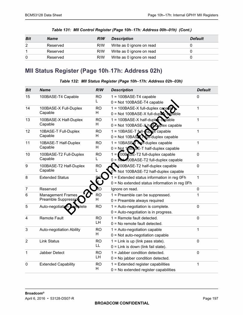
Page 10h–17h: Internal GPHY MII RegistersBCM53128 Data Sheet
BROADCOM CONFIDENTIAL
Broadcom®
April 6, 2016 • 53128-DS07-R Page 197
MII Status Register (Page 10h–17h: Address 02h)
2 Reserved R/W Write as 0 ignore on read 0
1 Reserved R/W Write as 0 ignore on read 0
0 Reserved R/W Write as 0 ignore on read 0
Table 132: MII Status Register (Page 10h–17h: Address 02h–03h)
Bit Name R/W Description Default
15 100BASE-T4 Capable ROL
1 = 100BASE-T4 capable0 = Not 100BASE-T4 capable
0
14 100BASE-X Full-DuplexCapable
ROH
1 = 100BASE-X full-duplex capable0 = Not 100BASE-X full-duplex capable
1
13 100BASE-X Half-DuplexCapable
ROH
1 = 100BASE-X half-duplex capable0 = Not 100BASE-X half-duplex capable
1
12 10BASE-T Full-DuplexCapable
ROH
1 = 10BASE-T full-duplex capable0 = Not 10BASE-T full-duplex capable
1
11 10BASE-T Half-DuplexCapable
ROH
1 = 10BASE-T half-duplex capable0 = Not 10BASE-T half-duplex capable
1
10 100BASE-T2 Full-DuplexCapable
ROL
1 = 100BASE-T2 full-duplex capable0 = Not 100BASE-T2 full-duplex capable
0
9 100BASE-T2 Half-DuplexCapable
ROL
1 = 100BASE-T2 half-duplex capable0 = Not 100BASE-T2 half-duplex capable
0
8 Extended Status ROH
1 = Extended status information in reg 0Fh0 = No extended status information in reg 0Fh
1
7 Reserved RO Ignore on read. 0
6 Management FramesPreamble Suppression
ROH
1 = Preamble can be suppressed.0 = Preamble always required
1
5 Auto-negotiation Complete RO 1 = Auto-negotiation is complete.0 = Auto-negotiation is in progress.
0
4 Remote Fault ROLH
1 = Remote fault detected.0 = No remote fault detected.
0
3 Auto-negotiation Ability ROH
1 = Auto-negotiation capable0 = Not auto-negotiation capable
1
2 Link Status ROLL
1 = Link is up (link pass state).0 = Link is down (link fail state).
0
1 Jabber Detect ROLH
1 = Jabber condition detected.0 = No jabber condition detected.
0
0 Extended Capability ROH
1 = Extended register capabilities0 = No extended register capabilities
1
Table 131: MII Control Register (Page 10h–17h: Address 00h–01h) (Cont.)
Bit Name R/W Description Default
Broadc
om C
onfid
entia
l
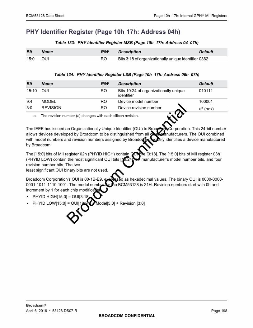
Page 10h–17h: Internal GPHY MII RegistersBCM53128 Data Sheet
BROADCOM CONFIDENTIAL
Broadcom®
April 6, 2016 • 53128-DS07-R Page 198
PHY Identifier Register (Page 10h–17h: Address 04h)
The IEEE has issued an Organizationally Unique Identifier (OUI) to Broadcom Corporation. This 24-bit numberallows devices developed by Broadcom to be distinguished from all other manufacturers. The OUI combinedwith model numbers and revision numbers assigned by Broadcom precisely identifies a device manufacturedby Broadcom.
The [15:0] bits of MII register 02h (PHYID HIGH) contain OUI bits [3:18]. The [15:0] bits of MII register 03h(PHYID LOW) contain the most significant OUI bits [19:24], six manufacturer’s model number bits, and fourrevision number bits. The twoleast significant OUI binary bits are not used.
Broadcom Corporation's OUI is 00-1B-E9, expressed as hexadecimal values. The binary OUI is 0000-0000-0001-1011-1110-1001. The model number for the BCM53128 is 21H. Revision numbers start with 0h andincrement by 1 for each chip modification.
• PHYID HIGH[15:0] = OUI[3:18]
• PHYID LOW[15:0] = OUI[19:24] + Model[5:0] + Revision [3:0]
Table 133: PHY Identifier Register MSB (Page 10h–17h: Address 04–07h)
Bit Name R/W Description Default
15:0 OUI RO Bits 3:18 of organizationally unique identifier 0362
Table 134: PHY Identifier Register LSB (Page 10h–17h: Address 06h–07h)
Bit Name R/W Description Default
15:10 OUI RO Bits 19:24 of organizationally uniqueidentifier
010111
9:4 MODEL RO Device model number 100001
3:0 REVISION RO Device revision number na (hex)
a. The revision number (n) changes with each silicon revision.
Broadc
om C
onfid
entia
l

Page 10h–17h: Internal GPHY MII RegistersBCM53128 Data Sheet
BROADCOM CONFIDENTIAL
Broadcom®
April 6, 2016 • 53128-DS07-R Page 199
Auto-Negotiation Advertisement Register (Page 10h–17h: Address08h)
Table 135: Auto-Negotiation Advertisement Register (Page 10h–17h: Address 08h–09h)
Bit Name R/W Description Default
15 Next Page R/W 1 = Next page ability is supported.0 = Next page ability is not supported.
0
14 Reserved R/W Write as 0, ignore on read. 0
13 Remote Fault R/W 1 = Advertise remote fault is detected.0 = Advertise no remote fault is detected.
0
12 Reserved Technology R/W Write as 0, ignore on read. 0
11 Asymmetric Pause R/W 1 = Advertise asymmetric pause0 = Advertise no asymmetric pause
1
10 Pause Capable R/W 1 = Capable of full-duplex pause operation0 = Not capable of pause operation
1
9 100BASE-T4 Capable R/W 1 = 100BASE-T4 capable0 = Not 100BASE-T4 capable
0
8 100BASE-TX Full-Duplex Capable
R/W 1 = 100BASE-TX full-duplex capable0 = Not 100BASE-TX full-duplex capable
1
7 100BASE-TX Half-Duplex Capable
R/W 1 = 100BASE-TX half-duplex capable0 = Not 100BASE-TX half-duplex capable
1
6 10BASE-T Full-DuplexCapable
R/W 1 = 10BASE-T full-duplex capable0 = Not 10BASE-T full-duplex capable
1
5 10BASE-T Half-DuplexCapable
R/W 1 = 10BASE-T half-duplex capable0 = Not 10BASE-T half-duplex capable
1
4 Protocol Selector Field R/W Bits [4:0] = 00001 indicatesIEEE 802.3 CSMA/CD
0
3 R/W 0
2 R/W 0
1 R/W 0
0 R/W 1Broadc
om C
onfid
entia
l
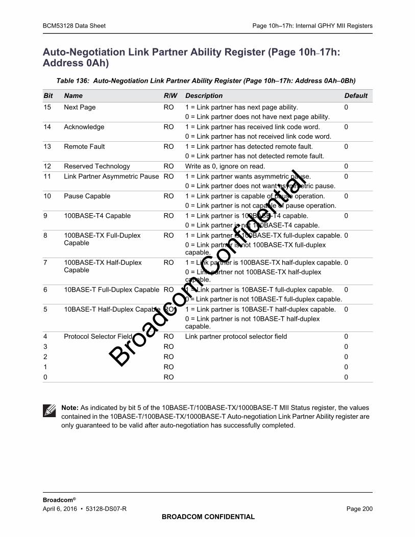
Page 10h–17h: Internal GPHY MII RegistersBCM53128 Data Sheet
BROADCOM CONFIDENTIAL
Broadcom®
April 6, 2016 • 53128-DS07-R Page 200
Auto-Negotiation Link Partner Ability Register (Page 10h–17h:Address 0Ah)
Table 136: Auto-Negotiation Link Partner Ability Register (Page 10h–17h: Address 0Ah–0Bh)
Bit Name R/W Description Default
15 Next Page RO 1 = Link partner has next page ability.0 = Link partner does not have next page ability.
0
14 Acknowledge RO 1 = Link partner has received link code word.0 = Link partner has not received link code word.
0
13 Remote Fault RO 1 = Link partner has detected remote fault.0 = Link partner has not detected remote fault.
0
12 Reserved Technology RO Write as 0, ignore on read. 0
11 Link Partner Asymmetric Pause RO 1 = Link partner wants asymmetric pause.0 = Link partner does not want asymmetric pause.
0
10 Pause Capable RO 1 = Link partner is capable of pause operation.0 = Link partner is not capable of pause operation.
0
9 100BASE-T4 Capable RO 1 = Link partner is 100BASE-T4 capable.0 = Link partner is not 100BASE-T4 capable.
0
8 100BASE-TX Full-DuplexCapable
RO 1 = Link partner is 100BASE-TX full-duplex capable.0 = Link partner is not 100BASE-TX full-duplexcapable.
0
7 100BASE-TX Half-DuplexCapable
RO 1 = Link partner is 100BASE-TX half-duplex capable.0 = Link partner not 100BASE-TX half-duplexcapable.
0
6 10BASE-T Full-Duplex Capable RO 1 = Link partner is 10BASE-T full-duplex capable.0 = Link partner is not 10BASE-T full-duplex capable.
0
5 10BASE-T Half-Duplex Capable RO 1 = Link partner is 10BASE-T half-duplex capable.0 = Link partner is not 10BASE-T half-duplexcapable.
0
4 Protocol Selector Field RO Link partner protocol selector field 0
3 RO 0
2 RO 0
1 RO 0
0 RO 0
Note: As indicated by bit 5 of the 10BASE-T/100BASE-TX/1000BASE-T MII Status register, the valuescontained in the 10BASE-T/100BASE-TX/1000BASE-T Auto-negotiation Link Partner Ability register areonly guaranteed to be valid after auto-negotiation has successfully completed.
Broadc
om C
onfid
entia
l
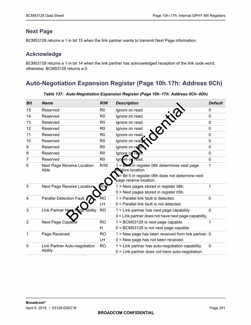
Page 10h–17h: Internal GPHY MII RegistersBCM53128 Data Sheet
BROADCOM CONFIDENTIAL
Broadcom®
April 6, 2016 • 53128-DS07-R Page 201
Next Page
BCM53128 returns a 1 in bit 15 when the link partner wants to transmit Next Page information.
Acknowledge
BCM53128 returns a 1 in bit 14 when the link partner has acknowledged reception of the link code word;otherwise, BCM53128 returns a 0.
Auto-Negotiation Expansion Register (Page 10h–17h: Address 0Ch)
Table 137: Auto-Negotiation Expansion Register (Page 10h–17h: Address 0Ch–0Dh)
Bit Name R/W Description Default
15 Reserved R0 Ignore on read. 0
14 Reserved R0 Ignore on read. 0
13 Reserved R0 Ignore on read. 0
12 Reserved R0 Ignore on read. 0
11 Reserved R0 Ignore on read. 0
10 Reserved R0 Ignore on read. 0
9 Reserved R0 Ignore on read. 0
8 Reserved R0 Ignore on read. 0
7 Reserved R0 Ignore on read. 0
6 Next Page Receive LocationAble
R/W 1 = Bit 5 in register 06h determines next pagereceive location.0 = Bit 5 in register 06h does not determine nextpage receive location.
1
5 Next Page Receive Location R/W 1 = Next pages stored in register 08h.0 = Next pages stored in register 05h.
1
4 Parallel Detection Fault ROLH
1 = Parallel link fault is detected.0 = Parallel link fault is not detected.
0
3 Link Partner Next Page Ability RO 1 = Link partner has next page capability.0 = Link partner does not have next page capability.
0
2 Next Page Capable ROH
1 = BCM53128 is next page capable.0 = BCM53128 is not next page capable.
1
1 Page Received ROLH
1 = New page has been received from link partner.0 = New page has not been received.
0
0 Link Partner Auto-negotiationAbility
RO 1 = Link partner has auto-negotiation capability.0 = Link partner does not have auto-negotiation.
0
Broadc
om C
onfid
entia
l

Page 10h–17h: Internal GPHY MII RegistersBCM53128 Data Sheet
BROADCOM CONFIDENTIAL
Broadcom®
April 6, 2016 • 53128-DS07-R Page 202
Next Page Transmit Register (Page 10h–17h: Address 0Eh)
Table 138: Next Page Transmit Register (Page 10h–17h: Address 0Eh–0Fh)
Bit Name R/W Description Default
15 Next Page R/W 1 = Additional next pages follow.0 = Sending last next page.
0
14 Reserved RO Ignore on read. 0
13 Message Page R/W 1 = Formatted page0 = Unformatted page
1
12 Acknowledge2 R/W 1 = Complies with message.0 = Cannot comply with message.Note: Not used with 1000BASE-T nextpages.
0
11 Toggle RO Toggles between exchanges of different nextpages.
0
10 Message/Unformatted CodeField
R/W Next page message code or unformatteddata
0
9 R/W 0
8 R/W 0
7 R/W 0
6 R/W 0
5 R/W 0
4 R/W 0
3 R/W 0
2 R/W 0
1 R/W 0
0 R/W 1
Broadc
om C
onfid
entia
l
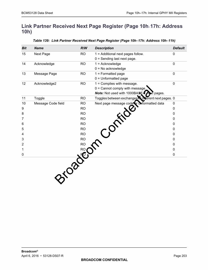
Page 10h–17h: Internal GPHY MII RegistersBCM53128 Data Sheet
BROADCOM CONFIDENTIAL
Broadcom®
April 6, 2016 • 53128-DS07-R Page 203
Link Partner Received Next Page Register (Page 10h–17h: Address10h)
Table 139: Link Partner Received Next Page Register (Page 10h–17h: Address 10h–11h)
Bit Name R/W Description Default
15 Next Page RO 1 = Additional next pages follow.0 = Sending last next page.
0
14 Acknowledge RO 1 = Acknowledge0 = No acknowledge
0
13 Message Page RO 1 = Formatted page0 = Unformatted page
0
12 Acknowledge2 RO 1 = Complies with message.0 = Cannot comply with message.Note: Not used with 1000BASE-T next pages.
0
11 Toggle RO Toggles between exchanges of different next pages. 0
10 Message Code field RO Next page message code or unformatted data 0
9 RO 0
8 RO 0
7 RO 0
6 RO 0
5 RO 0
4 RO 0
3 RO 0
2 RO 0
1 RO 0
0 RO 0
Broadc
om C
onfid
entia
l
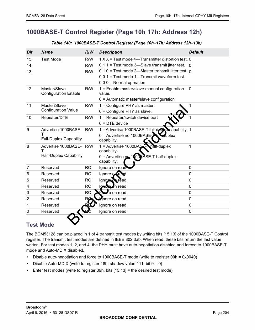
Page 10h–17h: Internal GPHY MII RegistersBCM53128 Data Sheet
BROADCOM CONFIDENTIAL
Broadcom®
April 6, 2016 • 53128-DS07-R Page 204
1000BASE-T Control Register (Page 10h–17h: Address 12h)
Test Mode
The BCM53128 can be placed in 1 of 4 transmit test modes by writing bits [15:13] of the 1000BASE-T Controlregister. The transmit test modes are defined in IEEE 802.3ab. When read, these bits return the last valuewritten. For test modes 1, 2, and 4, the PHY must have auto-negotiation disabled and forced to 1000BASE-Tmode and Auto-MDIX disabled.
• Disable auto-negotiation and force to 1000BASE-T mode (write to register 00h = 0x0040)
• Disable Auto-MDIX (write to register 18h, shadow value 111, bit 9 = 0)
• Enter test modes (write to register 09h, bits [15:13] = the desired test mode)
Table 140: 1000BASE-T Control Register (Page 10h–17h: Address 12h–13h)
Bit Name R/W Description Default
15 Test Mode R/W 1 X X = Test mode 4—Transmitter distortion test.0 1 1 = Test mode 3—Slave transmit jitter test.0 1 0 = Test mode 2—Master transmit jitter test.0 0 1 = Test mode 1—Transmit waveform test.0 0 0 = Normal operation
0
14 R/W 0
13 R/W 0
12 Master/SlaveConfiguration Enable
R/W 1 = Enable master/slave manual configurationvalue.0 = Automatic master/slave configuration
0
11 Master/SlaveConfiguration Value
R/W 1 = Configure PHY as master.0 = Configure PHY as slave.
1
10 Repeater/DTE R/W 1 = Repeater/switch device port0 = DTE device
1
9 Advertise 1000BASE-TFull-Duplex Capability
R/W 1 = Advertise 1000BASE-T full-duplex capability.0 = Advertise no 1000BASE-T full-duplexcapability.
1
8 Advertise 1000BASE-THalf-Duplex Capability
R/W 1 = Advertise 1000BASE-T half-duplexcapability.0 = Advertise no 1000BASE-T half-duplexcapability.
1
7 Reserved RO Ignore on read. 0
6 Reserved RO Ignore on read. 0
5 Reserved RO Ignore on read. 0
4 Reserved RO Ignore on read. 0
3 Reserved RO Ignore on read. 0
2 Reserved RO Ignore on read. 0
1 Reserved RO Ignore on read. 0
0 Reserved RO Ignore on read. 0
Broadc
om C
onfid
entia
l

Page 10h–17h: Internal GPHY MII RegistersBCM53128 Data Sheet
BROADCOM CONFIDENTIAL
Broadcom®
April 6, 2016 • 53128-DS07-R Page 205
Master/Slave Configuration Enable
When bit 12 is set = 1, the BCM53128 master/slave mode is configured using the manual master/slaveconfiguration value. When the bit is cleared, the master/slave mode is configured using the automatic resolutionfunction. This bit returns a 1 when manual master/slave configuration is enabled; otherwise, it returns a 0.
1000BASE-T Status Register (Page 10h–17h: Address 14h)
Table 141: 1000BASE-T Status Register (Page 10h–17h: Address 14h–15h)
Bit Name R/W Description Default
15 Master/Slave Configuration Fault ROLH
1 = Master/slave configuration fault detected.0 = No master/slave configuration fault detected.
0
14 Master/Slave ConfigurationResolution
RO 1 = Local transmitter is master.0 = Local transmitter is slave.
0
13 Local Receiver Status RO 1 = Local receiver is OK.0 = Local receiver is not OK.
0
12 Remote Receiver Status RO 1 = Remote receiver is OK.0 = Remote receiver is not OK.
0
11 Link Partner 1000BASE-TFull-Duplex Capability
RO 1 = Link partner is 1000BASE-T full-duplexcapable.0 = Link partner is not 1000BASE-T full-duplexcapable.
0
10 Link Partner 1000BASE-THalf-Duplex Capability
RO 1 = Link partner is 1000BASE-T half-duplexcapable.0 = Link partner is not 1000BASE-T half-duplexcapable.
0
9 Reserved RO Ignore on read. 0
8 Reserved RO Ignore on read. 0
7 Idle Error Count ROCR
Number of idle errors since last read 0
6 ROCR
0
5 ROCR
0
4 ROCR
0
3 ROCR
0
2 ROCR
0
1 ROCR
0
0 ROCR
0
Broadc
om C
onfid
entia
l
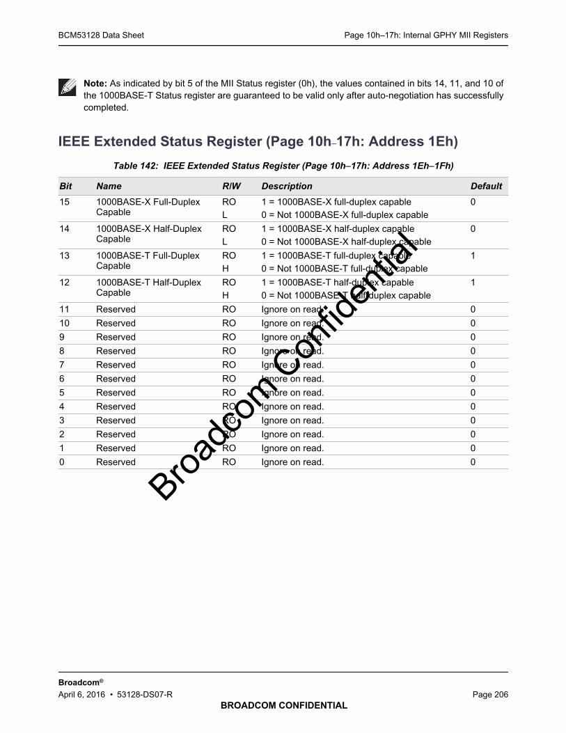
Page 10h–17h: Internal GPHY MII RegistersBCM53128 Data Sheet
BROADCOM CONFIDENTIAL
Broadcom®
April 6, 2016 • 53128-DS07-R Page 206
IEEE Extended Status Register (Page 10h–17h: Address 1Eh)
Note: As indicated by bit 5 of the MII Status register (0h), the values contained in bits 14, 11, and 10 ofthe 1000BASE-T Status register are guaranteed to be valid only after auto-negotiation has successfullycompleted.
Table 142: IEEE Extended Status Register (Page 10h–17h: Address 1Eh–1Fh)
Bit Name R/W Description Default
15 1000BASE-X Full-DuplexCapable
ROL
1 = 1000BASE-X full-duplex capable0 = Not 1000BASE-X full-duplex capable
0
14 1000BASE-X Half-DuplexCapable
ROL
1 = 1000BASE-X half-duplex capable0 = Not 1000BASE-X half-duplex capable
0
13 1000BASE-T Full-DuplexCapable
ROH
1 = 1000BASE-T full-duplex capable0 = Not 1000BASE-T full-duplex capable
1
12 1000BASE-T Half-DuplexCapable
ROH
1 = 1000BASE-T half-duplex capable0 = Not 1000BASE-T half-duplex capable
1
11 Reserved RO Ignore on read. 0
10 Reserved RO Ignore on read. 0
9 Reserved RO Ignore on read. 0
8 Reserved RO Ignore on read. 0
7 Reserved RO Ignore on read. 0
6 Reserved RO Ignore on read. 0
5 Reserved RO Ignore on read. 0
4 Reserved RO Ignore on read. 0
3 Reserved RO Ignore on read. 0
2 Reserved RO Ignore on read. 0
1 Reserved RO Ignore on read. 0
0 Reserved RO Ignore on read. 0
Broadc
om C
onfid
entia
l

Page 10h–17h: Internal GPHY MII RegistersBCM53128 Data Sheet
BROADCOM CONFIDENTIAL
Broadcom®
April 6, 2016 • 53128-DS07-R Page 207
PHY Extended Control Register (Page 10h–17h: Address 20h)
Table 143: PHY Extended Control Register (Page 10h–17h: Address 20h–21h)
Bit Name R/W Description Default
15 Reserved R/W Write as 0, ignore on read. 0
14 Disable Automatic MDICrossover
R/W 1 = Automatic MDI crossover is disabled.0 = Automatic MDI crossover is enabled.
0
13 Transmit Disable R/W 1 = Transmitter outputs are disabled.0 = Normal operation
0
12:11 Reserved – – –
10 Bypass 4B/5B Encoder/Decoder (100BASE-T)
R/W 1 = Transmit and receive 5B codes over MIIpins.0 = Normal MII
0
9 BypassScrambler/Descrambler(100BASE-T)
R/W 1 = Scrambler and descrambler are disabled.0 = Scrambler and descrambler are enabled.
0
8 Bypass NRZI/MLT3 Encoder/Decoder (100BASE-T)
R/W 1 = Bypass NRZI/MLT3 encoder and decoder.0 = Normal operation
0
7 Bypass Receive SymbolAlignment (100BASE-T)
R/W 1 = The 5B receive symbols are not aligned.0 = Receive symbols aligned to 5B boundaries
0
6 Reset Scrambler (100BASE-T) R/WSC
1 = Reset scrambler to initial state.0 = Normal scrambler operation
0
5:3 Reserved – – –
2 Reserved R/W Write as 0, ignore on read. 0
1 Reserved R/W Write as 0, ignore on read. 0
0 1000 Mbps PCS Transmit FIFOElasticity
R/W 1 = High latency0 = Low latency
0
Broadc
om C
onfid
entia
l

Page 10h–17h: Internal GPHY MII RegistersBCM53128 Data Sheet
BROADCOM CONFIDENTIAL
Broadcom®
April 6, 2016 • 53128-DS07-R Page 208
PHY Extended Status Register (Page 10h–17h: Address 22h)
Table 144: PHY Extended Status Register (Page 10h–17h: Address 22h–23h)
Bit Name R/W Description Default
15 Auto-negotiation Base PageSelector Field Mismatch
ROLH
1 = Link partner base page selector fieldmismatched advertised selector field since lastread.0 = No mismatch detected since last read.
0
14 Ethernet@WireSpeedDowngrade
RO 1 = Auto-negotiation advertised speed downgraded0 = No advertised speed downgrade
0
13 MDI Crossover State RO 1 = Crossover MDI mode0 = Normal MDI mode
0
12 Interrupt Status RO 1 = Unmasked interrupt is currently active.0 = Interrupt is cleared.
0
11 Remote Receiver Status ROLL
1 = Remote receiver is OK.0 = Remote receiver is not OK since last read
0
10 Local Receiver Status ROLL
1 = Local receiver is OK.0 = Local receiver is not OK since last read.
0
9 Locked RO 1 = Descrambler is locked.0 = Descrambler is unlocked.
0
8 Link Status RO 1 = Link pass0 = Link fail
0
7 CRC Error Detected ROLH
1 = CRC error detected.0 = No CRC error since last read.
0
6 Carrier Extension ErrorDetected
ROLH
1 = Carrier extension error detected since last read.0 = No carrier extension error since last read.
0
5 Bad SSD Detected(False Carrier)
ROLH
1 = Bad SSD error detected since last read.0 = No bad SSD error since last read.
0
4 Bad ESD Detected(Premature End)
ROLH
1 = Bad ESD error detected since last read.0 = No bad ESD error since last read.
0
3 Receive Error Detected ROLH
1 = Receive error detected since last read.0 = No receive error since last read.
0
2 Transmit Error Detected ROLH
1 = Transmit error code received since last read.0 = No transmit error code received since last read.
0
1 Lock Error Detected ROLH
1 = Lock error detected since last read.0 = No lock error since last read.
0
0 MLT3 Code Error Detected ROLH
1 = MLT3 code error detected since last read.0 = No MLT3 code error since last read.
0
Broadc
om C
onfid
entia
l

Page 10h–17h: Internal GPHY MII RegistersBCM53128 Data Sheet
BROADCOM CONFIDENTIAL
Broadcom®
April 6, 2016 • 53128-DS07-R Page 209
Receive Error Counter Register (Page 10h–17h: Address 24h)
Copper Receive Error Counter
When bit 9 = 0 in register 38h, shadow value 11011, this counter increments each time BCM53128 receives a10BASE-T, 100BASE-TX, 1000BASE-T noncollision packet containing at least one receive error. This counterfreezes at the maximum value of FFFFh. The counter automatically clears when read.
False Carrier Sense Counter Register (Page 10h–17h: Address 26h)
Copper False Carrier Sense Counter
When bit 9 = 0 in register 1Ch, shadow value 11011 and bit 14 = 0 in register 3Ch, the False Carrier SenseCounter increments each time the BCM53128 detects a 10BASE-T, 100BASE-TX, 1000BASE-T false carriersense on the receive input. This counter freezes at the maximum value of FFh. The counter automatically clearswhen read.
Table 145: Receive Error Counter Register (Page 10h–17h: Address 24h–25h)a
a. Bits 15:0 of this register become the 10BASE-T, 100BASE-TX, 1000BASE-T Receive Error Counter whenregister 38h, shadow value11011, bit 9 = 0.
Bit Name R/W Description Default
15:0 Receive Error Counter R/WCR
The number of noncollision packets with receiveerrors since last read
0000h
Table 146: False Carrier Sense Counter Register (Page 10h–17h: Address 26h–27h)a
a. Bits 7:0 of this register become the 10BASE-T/100BASE-TX/1000BASE-T Carrier Sense Counter whenregister 38h, shadow 11011, bit 9 = 0 and register 3Ch, bit 14 = 0.
Bit Name R/W Description Default
15:8 Reserved RO Ignore on read. 00h
7:0 False Carrier Sense Counter R/WCR
The number of false carrier sense events since lastread.
00h
Broadc
om C
onfid
entia
l

Page 10h–17h: Internal GPHY MII RegistersBCM53128 Data Sheet
BROADCOM CONFIDENTIAL
Broadcom®
April 6, 2016 • 53128-DS07-R Page 210
10BASE-T/100BASE-TX/1000BASE-T Packets Received withTransmit Error Codes Counter
Packets Received with Transmit Error Codes Counter
The BCM53128 detects a 10BASE-T/100BASE-TX/1000BASE-T packet with a transmit error code violationwhen bit 9 = 0 in register 38h, shadow value 11011, and when bit 14 = 1 in register 1Eh, Packets Received withTransmit Error Codes Counter increments each time. This counter freezes at the maximum value of FFh. Thecounter automatically clears when read.
Receiver NOT_OK Counter Register (Page 10h–17h: Address 28h)
Copper Local Receiver NOT_OK Counter
When bit 9 = 0 in register 38h, shadow value 11011 and bit 15 = 0 in register 3Ch, this counter increments eachtime the 10BASE-T, 100BASE-TX, or 1000BASE-T local receiver enters the NOT_OK state. This counterfreezes at the maximum value of FFh. The counter automatically clears when read.
Copper Remote Receiver NOT_OK Counter
When bit 9 = 0 in register 38h, shadow value 11011 and bit 15 = 0 in register 3Ch, this counter increments eachtime the 1000BASE-T, 100BASE-TX, or 10BASE-T remote receiver enters the NOT_OK state. This counterfreezes at the maximum value of FFh. The counter automatically clears when read.
Table 147: 10BASE-T/100BASE-TX/1000BASE-T Transmit Error Code Counter Register (Address 13h)a
a. Bits 7:0 of this register become the 10BASE-T/100BASE-TX/1000BASE-T packets received with transmiterror codes counter when register 38h, shadow 11011, bit 9 = 0 and register 3Ch, bit 14 = 1.
Bit Name R/W Description Default
15:8 Reserved RO Write as 0, ignore on read. 00h
7:0 Transmit Error Code Counter R/WCR
The number of packets received with transmit errorcodes since last read.
00h
Table 148: Receiver NOT_OK Counter Register (Page 10h–17h: Address 28h–29h)a
a. Bits 15:0 of this register become the 10BASE-T, 100BASE-TX, or 1000BASE-T Receiver NOT_OK Counterwhen register 38h, shadow 11011, bit 9 = 0 and register 3Ch bit 15 = 0.
Bit Name R/W Description Default
15:8 Local Receiver NOT_OKCounter
R/WCR
The number of times local receiver was NOT_OKsince last read.
00h
7:0 Remote Receiver NOT_OKCounter
R/WCR
The number of times BCM53128 detected that theremote receiver was NOT_OK since last read.
00h
Broadc
om C
onfid
entia
l

Page 10h–17h: Internal GPHY MII RegistersBCM53128 Data Sheet
BROADCOM CONFIDENTIAL
Broadcom®
April 6, 2016 • 53128-DS07-R Page 211
Receive CRC Counter Register (Page 10h–17h: Address 28h)
Copper CRC Counter
When bit 9 = 0 in register 38h, shadow value 11011 and bit 15 = 1 in register 3Ch, this counter increments eachtime the 10BASE-T, 100BASE-TX, or 1000BASE-T detects a receive CRC error. This counter freezes at themaximum value of FFh. The counter automatically clears when read.
Expansion Register Access Register (Page 10h–17h: Address 2Eh)
Expansion Register Select
Setting bits [11:8] to 1111 enables the reading from and writing to the Expansion registers in conjunction withregister 2Ah. These bits should be cleared after the Expansion registers are accessed or when the Expansionregisters are not being accessed. See “Expansion Registers” on page 229 for Expansion register detail.
Table 149: CRC Counter Register (Page 10h–17h: Address 28h–29h)a
a. Bits 15:0 of this register become the 10BASE-T, 100BASE-TX, or 1000BASE-T Receive CRC Counter whenregister 38h, shadow 11011, bit 9 = 0 and register 3Ch bit 15 = 1.
Bit Name R/W Description Default
15:0 Receive CRC Counter R/WCR
The number of times receive CRC errors weredetected.
00h
Table 150: Expansion Register Access Register (Page 10h–17h: Address 2Eh–2Fh)
Bit Name R/W Description Default
15 Reserved R/W Write as 0, ignore on read. 0
14 Reserved R/W Write as 0, ignore on read. 0
13 Reserved R/W Write as 0, ignore on read. 0
12 Reserved R/W Write as 0, ignore on read. 0
11 Expansion Register Select R/W 1111 = Expansion register is selected.0000 = Expansion register is not selected.
All others = Reserved (Do not use)
0
10 R/W 0
9 R/W 0
8 R/W 0
7 Expansion Register Accessed R/W Sets the expansion register number accessedwhen read/write to register 2Ah.
0
6 R/W 0
5 R/W 0
4 R/W 0
3 R/W 0
2 R/W 0
1 R/W 0
0 R/W 0
Broadc
om C
onfid
entia
l
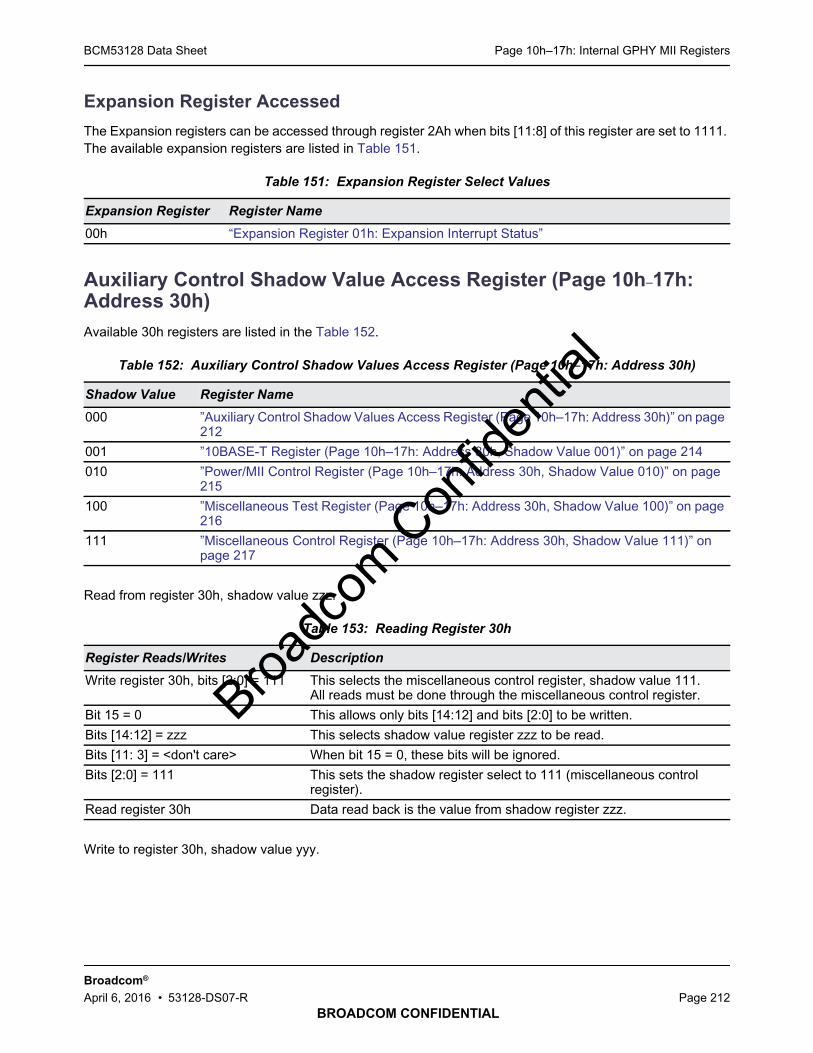
Page 10h–17h: Internal GPHY MII RegistersBCM53128 Data Sheet
BROADCOM CONFIDENTIAL
Broadcom®
April 6, 2016 • 53128-DS07-R Page 212
Expansion Register Accessed
The Expansion registers can be accessed through register 2Ah when bits [11:8] of this register are set to 1111.The available expansion registers are listed in Table 151.
Auxiliary Control Shadow Value Access Register (Page 10h–17h:Address 30h)
Available 30h registers are listed in the Table 152.
Read from register 30h, shadow value zzz.
Write to register 30h, shadow value yyy.
Table 151: Expansion Register Select Values
Expansion Register Register Name
00h “Expansion Register 01h: Expansion Interrupt Status”
Table 152: Auxiliary Control Shadow Values Access Register (Page 10h–17h: Address 30h)
Shadow Value Register Name
000 ”Auxiliary Control Shadow Values Access Register (Page 10h–17h: Address 30h)” on page212
001 ”10BASE-T Register (Page 10h–17h: Address 30h, Shadow Value 001)” on page 214
010 ”Power/MII Control Register (Page 10h–17h: Address 30h, Shadow Value 010)” on page215
100 ”Miscellaneous Test Register (Page 10h–17h: Address 30h, Shadow Value 100)” on page216
111 ”Miscellaneous Control Register (Page 10h–17h: Address 30h, Shadow Value 111)” onpage 217
Table 153: Reading Register 30h
Register Reads/Writes Description
Write register 30h, bits [2:0] = 111 This selects the miscellaneous control register, shadow value 111.All reads must be done through the miscellaneous control register.
Bit 15 = 0 This allows only bits [14:12] and bits [2:0] to be written.
Bits [14:12] = zzz This selects shadow value register zzz to be read.
Bits [11: 3] = <don't care> When bit 15 = 0, these bits will be ignored.
Bits [2:0] = 111 This sets the shadow register select to 111 (miscellaneous controlregister).
Read register 30h Data read back is the value from shadow register zzz.
Broadc
om C
onfid
entia
l

Page 10h–17h: Internal GPHY MII RegistersBCM53128 Data Sheet
BROADCOM CONFIDENTIAL
Broadcom®
April 6, 2016 • 53128-DS07-R Page 213
External Loopback
When bit 15 = 1, external loopback operation is enabled. When the bit is cleared, normal operation resumes.
Table 154: Writing Register 30h
Register Writes Description
Set Bits [15:3] = Preferred write values Bits [15:3] contain the values to which the desired bits are written.
Set Bits [2:0] = yyy This enables shadow value register yyy to be written. For shadowvalue 111, bit 15 must also be written.
Table 155: Auxiliary Control Register (Page 10h–17h: Address 30h, Shadow Value 000)
Bit Name R/W Description Default
15 External Loopback R/W 1 = External Loopback is enabled0 = Normal operation
0
14 Receive ExtendedPacket Length
R/W 1 = Allow reception of extended length packets.0 = Allow reception of normal length Ethernet packetsonly.
0
13 Edge Rate Control(1000BASE-T)
R/W 00 = 4.0 ns01 = 5.0 ns10 = 3.0 ns11 = 0.0 ns
0
12 R/W 0
11 Reserved R/W Write as 0, ignore on read. 0
10 Reserved R/W Write as 1, ignore on read. 1
9 Reserved R/W Write as 0, ignore on read. 0
8 Reserved R/W Write as 0, ignore on read. 0
7 Reserved R/W Write as 0, ignore on read. 0
6 Reserved R/W Write as 0, ignore on read. 0
5 Edge Rate Control(100BASE-TX)
R/W 00 = 4.0 ns01 = 5.0 ns10 = 3.0 ns11 = 0.0 ns
0
4 R/W 0
3 Reserved R/W Write as 0, ignore on read 0
2 Shadow Register Select R/W 000 = Auxiliary control register001 = 10BASE-T register010 = Power/MII control register100 = Miscellaneous test register111 = Miscellaneous control register
0
1 R/W 0
0 R/W 0Broadc
om C
onfid
entia
l

Page 10h–17h: Internal GPHY MII RegistersBCM53128 Data Sheet
BROADCOM CONFIDENTIAL
Broadcom®
April 6, 2016 • 53128-DS07-R Page 214
Receive Extended Packet Length
When bit 14 = 1, BCM53128 can receive packets up to 9720 bytes in length when in SGMII mode.
When the bit is cleared, the BCM53128 only receives packets up to standard maximum size in length.
Edge Rate Control (1000BASE-T)
Bits [13:12] control the edge rate of the 1000BASE-T transmit DAC output waveform.
Edge Rate Control (100BASE-TX)
Bits [5:4] control the edge rate of the 100BASE-TX transmit DAC output waveform.
Shadow Register Select
See the note on “Auxiliary Control Shadow Values Access Register (Page 10h–17h: Address 30h)” on page 212describing reading from and writing to register 18h.
The register set shown above is that for normal operation obtained when the lower 3 bits are 000.
10BASE-T Register
Table 156: 10BASE-T Register (Page 10h–17h: Address 30h, Shadow Value 001)
Bit Name R/W Description Default
15 Manchester Code Error ROLH
1 = Manchester code error (10BASE-T)0 = No Manchester code error
0
14 EOF Error ROLH
1 = EOF error is detected (10BASE-T).0 = No EOF error is detected.
0
13 Polarity Error RO 1 = Channel polarity is inverted.0 = Channel polarity is correct.
0
12 Block RX_DV Extension (IPG) R/W 1 = Block RX_DV for four additional RXC cycles forIPG.0 = Normal operation
0
11 10BASE-T TXC Invert Mode R/W 1 = Invert TXC output.0 = Normal operation
0
10 Reserved R/W Write as 0, ignore on read 0
9 Jabber Disable R/W 1 = Jabber function is disabled.0 = Jabber function is enabled
0
8 Reserved R/W Write as 0, ignore on read. 0
7 Reserved R/W Write as 0, ignore on read. 0
6 10BASE-T Echo Mode R/W 1 = Echo transmit data to receive data0 = Normal operation
0
Broadc
om C
onfid
entia
l
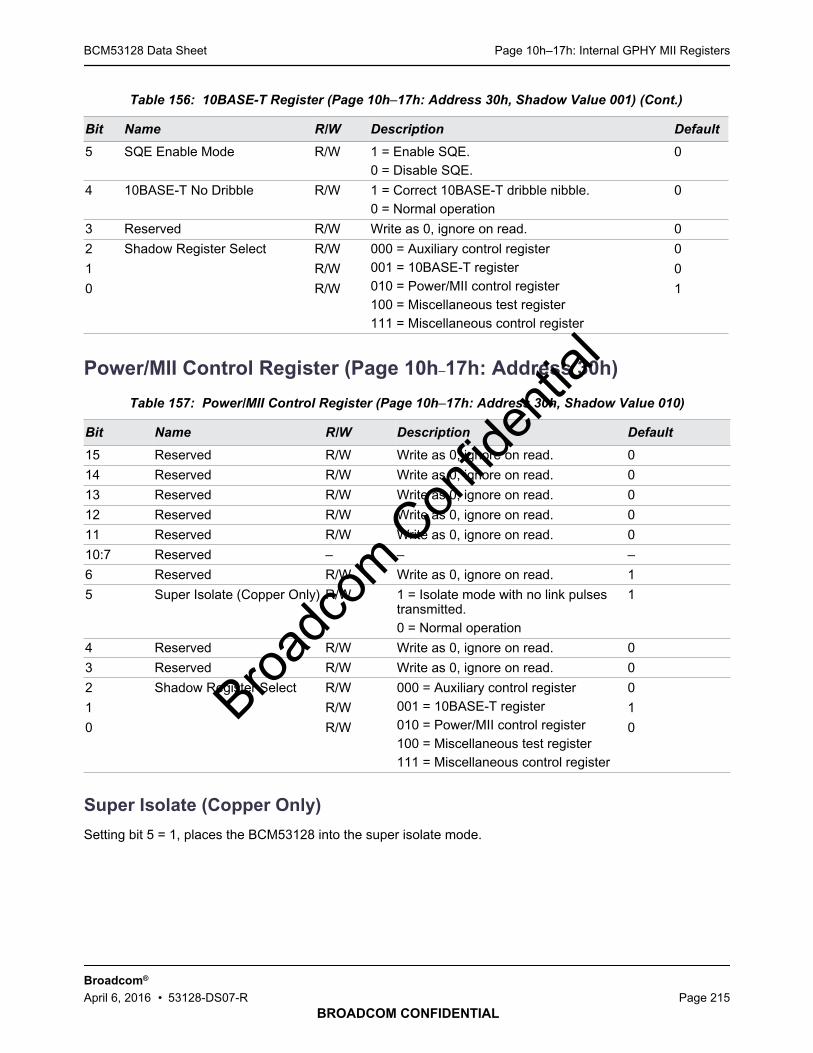
Page 10h–17h: Internal GPHY MII RegistersBCM53128 Data Sheet
BROADCOM CONFIDENTIAL
Broadcom®
April 6, 2016 • 53128-DS07-R Page 215
Power/MII Control Register (Page 10h–17h: Address 30h)
Super Isolate (Copper Only)
Setting bit 5 = 1, places the BCM53128 into the super isolate mode.
5 SQE Enable Mode R/W 1 = Enable SQE.0 = Disable SQE.
0
4 10BASE-T No Dribble R/W 1 = Correct 10BASE-T dribble nibble.0 = Normal operation
0
3 Reserved R/W Write as 0, ignore on read. 0
2 Shadow Register Select R/W 000 = Auxiliary control register001 = 10BASE-T register010 = Power/MII control register100 = Miscellaneous test register111 = Miscellaneous control register
0
1 R/W 0
0 R/W 1
Table 157: Power/MII Control Register (Page 10h–17h: Address 30h, Shadow Value 010)
Bit Name R/W Description Default
15 Reserved R/W Write as 0, ignore on read. 0
14 Reserved R/W Write as 0, ignore on read. 0
13 Reserved R/W Write as 0, ignore on read. 0
12 Reserved R/W Write as 0, ignore on read. 0
11 Reserved R/W Write as 0, ignore on read. 0
10:7 Reserved – – –
6 Reserved R/W Write as 0, ignore on read. 1
5 Super Isolate (Copper Only) R/W 1 = Isolate mode with no link pulsestransmitted.0 = Normal operation
1
4 Reserved R/W Write as 0, ignore on read. 0
3 Reserved R/W Write as 0, ignore on read. 0
2 Shadow Register Select R/W 000 = Auxiliary control register001 = 10BASE-T register010 = Power/MII control register100 = Miscellaneous test register111 = Miscellaneous control register
0
1 R/W 1
0 R/W 0
Table 156: 10BASE-T Register (Page 10h–17h: Address 30h, Shadow Value 001) (Cont.)
Bit Name R/W Description Default
Broadc
om C
onfid
entia
l
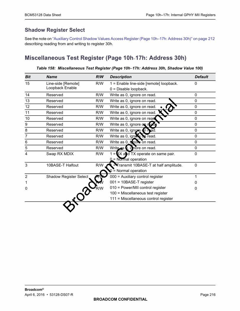
Page 10h–17h: Internal GPHY MII RegistersBCM53128 Data Sheet
BROADCOM CONFIDENTIAL
Broadcom®
April 6, 2016 • 53128-DS07-R Page 216
Shadow Register Select
See the note on “Auxiliary Control Shadow Values Access Register (Page 10h–17h: Address 30h)” on page 212describing reading from and writing to register 30h.
Miscellaneous Test Register (Page 10h–17h: Address 30h)
Table 158: Miscellaneous Test Register (Page 10h–17h: Address 30h, Shadow Value 100)
Bit Name R/W Description Default
15 Line-side [Remote]Loopback Enable
R/W 1 = Enable line-side [remote] loopback.0 = Disable loopback.
0
14 Reserved R/W Write as 0, ignore on read. 0
13 Reserved R/W Write as 0, ignore on read. 0
12 Reserved R/W Write as 0, ignore on read. 0
11 Reserved R/W Write as 0, ignore on read. 0
10 Reserved R/W Write as 0, ignore on read. 0
9 Reserved R/W Write as 0, ignore on read. 0
8 Reserved R/W Write as 0, ignore on read. 0
7 Reserved R/W Write as 0, ignore on read. 0
6 Reserved R/W Write as 0, ignore on read. 0
5 Reserved R/W Write as 0, ignore on read. 0
4 Swap RX MDIX R/W 1 = RX and TX operate on same pair.0 = Normal operation
0
3 10BASE-T Halfout R/W 1 = Transmit 10BASE-T at half amplitude.0 = Normal operation
0
2 Shadow Register Select R/W 000 = Auxiliary control register001 = 10BASE-T register010 = Power/MII control register100 = Miscellaneous test register111 = Miscellaneous control register
1
1 R/W 0
0 R/W 0
Broadc
om C
onfid
entia
l

Page 10h–17h: Internal GPHY MII RegistersBCM53128 Data Sheet
BROADCOM CONFIDENTIAL
Broadcom®
April 6, 2016 • 53128-DS07-R Page 217
Miscellaneous Control Register (Page 10h–17h: Address 30h)
Table 159: Miscellaneous Control Register (Page 10h–17h: Address 30h, Shadow Value 111)
Bit Name R/W Description Default
15 Write Enable R/WSC
1 = Write bits [14:3]0 = Only write bits [14:12]
0
14 Shadow Register ReadSelector
R/W These bits are written when bit 15 is not set. Thissets the shadow value for address 18h registerread.000 = Normal operation001 = 10BASE-T register010 = Power control register100 = Miscellaneous test register111 = Miscellaneous control register
0
13 R/W 0
12 R/W 0
11 Packet Counter Mode R/W 1 = Receive packet counter.0 = Transmit packet counter.
0
10 Reserved R/W Write as 0, ignore on read. 0
9 Force Auto-MDIX Mode R/W 1 = Auto-MDIX is enabled when auto-negotiationis disabled.0 = Auto-MDIX is disabled when auto-negotiationis disabled.
0
8 Reserved R/W Write as 0, ignore on read. 0
7 Reserved R/W Write as 0, ignore on read. 0
6 Reserved R/W Write as 0, ignore on read. 0
5 Reserved R/W Write as 0, ignore on read. 0
4 Ethernet@WireSpeed Enable R/W 1 = Enable Ethernet@WireSpeed0 = Disable Ethernet@WireSpeed
1
3 MDIO All PHY Select R/W 1 = The PHY ports accepts MDIO writes to PHYaddress = 00000.0 = Normal operation
0
2 Shadow Register Select R/W 000 = Auxiliary control register001 = 10BASE-T register010 = Power/MII control register100 = Miscellaneous test register111 = Miscellaneous control register
1
1 R/W 1
0 R/W 1Broadc
om C
onfid
entia
l

Page 10h–17h: Internal GPHY MII RegistersBCM53128 Data Sheet
BROADCOM CONFIDENTIAL
Broadcom®
April 6, 2016 • 53128-DS07-R Page 218
Auxiliary Status Summary Register (Page 10h–17h: Address 32h)
Table 160: Auxiliary Status Summary Register (Page 10h–17h: Address 32h–33h)
Bit Name R/W Description Default
15 Auto-negotiation Complete RO 1 = Auto-negotiation is complete.0 = Auto-negotiation is in progress.
0
14 Auto-negotiation CompleteAcknowledge
ROLH
1 = Entered auto-negotiation link is good check state.0 = State not entered since last read.
0
13 Auto-negotiation AcknowledgeDetect
ROLH
1 = Entered auto-negotiation acknowledge detectstate.0 = State not entered since last read
0
12 Auto-negotiation Ability Detect ROLH
1 = Entered auto-negotiation ability detect state.0 = State not entered since last read.
0
11 Auto-negotiation Next PageWait
ROLH
1 = Entered auto-negotiation next page wait state.0 = State not entered since last read.
0
10 Auto-negotiation HCDCurrent Operating Speed andDuplex Mode
RO 111 = 1000BASE-T full-duplexa
110 = 1000BASE-T half-duplexa
101 = 100BASE-TX full-duplexa
100 = 100BASE-T4
011 = 100BASE-TX half-duplexa
010 = 10BASE-T full-duplexa
001 = 10BASE-T half-duplexa
000 = No highest common denominator orauto-negotiation is incomplete.
a. Indicates the negotiated HCD when Auto-negotiation Enable = 1, or indicates the manually selected speedand duplex mode when Auto-negotiation Enable = 0.
0
9 RO 0
8 RO 0
7 Parallel Detection Fault ROLH
1 = Parallel link fault is detected.0 = Parallel link fault is not detected.
0
6 Remote Fault RO 1 = Link partner has detected a remote fault.0 = Link partner has not detected a remote fault.
0
5 Auto-negotiation PageReceived
ROLH
1 = New page has been received from the link partner.0 = New page has not been received.
0
4 Link Partner Auto-negotiationAbility
RO 1 = Link partner has auto-negotiation capability.0 = Link partner does not perform auto-negotiation.
0
3 Link Partner Next Page Ability RO 1 = Link partner has next page capability.0 = Link partner does not have next page capability.
0
2 Link Status RO 1 = Link is up (link pass state).0 = Link is down (link fail state).
0
1 Pause Resolution—ReceiveDirection
RO 1 = Enable pause receive.0 = Disable pause receive.
0
0 Pause Resolution—TransmitDirection
RO 1 = Enable pause transmit.0 = Disable pause transmit.
0
Broadc
om C
onfid
entia
l
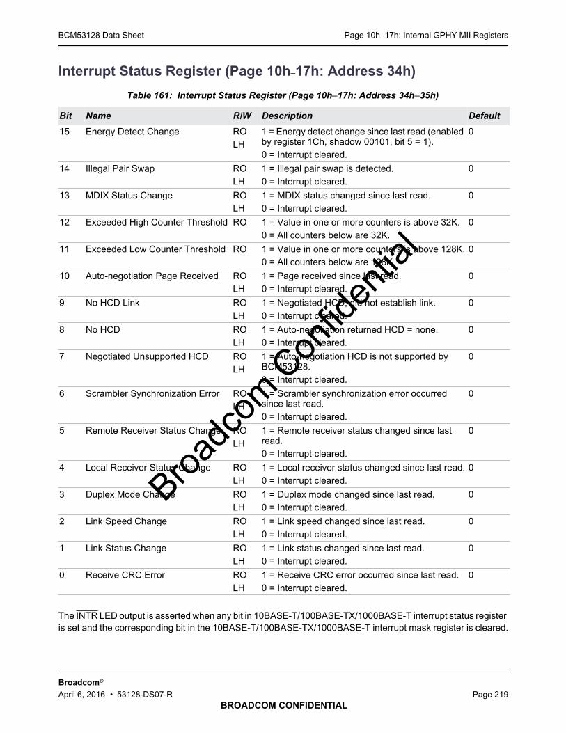
Page 10h–17h: Internal GPHY MII RegistersBCM53128 Data Sheet
BROADCOM CONFIDENTIAL
Broadcom®
April 6, 2016 • 53128-DS07-R Page 219
Interrupt Status Register (Page 10h–17h: Address 34h)
The INTR LED output is asserted when any bit in 10BASE-T/100BASE-TX/1000BASE-T interrupt status registeris set and the corresponding bit in the 10BASE-T/100BASE-TX/1000BASE-T interrupt mask register is cleared.
Table 161: Interrupt Status Register (Page 10h–17h: Address 34h–35h)
Bit Name R/W Description Default
15 Energy Detect Change ROLH
1 = Energy detect change since last read (enabledby register 1Ch, shadow 00101, bit 5 = 1).0 = Interrupt cleared.
0
14 Illegal Pair Swap ROLH
1 = Illegal pair swap is detected.0 = Interrupt cleared.
0
13 MDIX Status Change ROLH
1 = MDIX status changed since last read.0 = Interrupt cleared.
0
12 Exceeded High Counter Threshold RO 1 = Value in one or more counters is above 32K.0 = All counters below are 32K.
0
11 Exceeded Low Counter Threshold RO 1 = Value in one or more counters is above 128K.0 = All counters below are 128K.
0
10 Auto-negotiation Page Received ROLH
1 = Page received since last read.0 = Interrupt cleared.
0
9 No HCD Link ROLH
1 = Negotiated HCD, did not establish link.0 = Interrupt cleared.
0
8 No HCD ROLH
1 = Auto-negotiation returned HCD = none.0 = Interrupt cleared.
0
7 Negotiated Unsupported HCD ROLH
1 = Auto-negotiation HCD is not supported byBCM53128.0 = Interrupt cleared.
0
6 Scrambler Synchronization Error ROLH
1 = Scrambler synchronization error occurredsince last read.0 = Interrupt cleared.
0
5 Remote Receiver Status Change ROLH
1 = Remote receiver status changed since lastread.0 = Interrupt cleared.
0
4 Local Receiver Status Change ROLH
1 = Local receiver status changed since last read.0 = Interrupt cleared.
0
3 Duplex Mode Change ROLH
1 = Duplex mode changed since last read.0 = Interrupt cleared.
0
2 Link Speed Change ROLH
1 = Link speed changed since last read.0 = Interrupt cleared.
0
1 Link Status Change ROLH
1 = Link status changed since last read.0 = Interrupt cleared.
0
0 Receive CRC Error ROLH
1 = Receive CRC error occurred since last read.0 = Interrupt cleared.
0
Broadc
om C
onfid
entia
l

Page 10h–17h: Internal GPHY MII RegistersBCM53128 Data Sheet
BROADCOM CONFIDENTIAL
Broadcom®
April 6, 2016 • 53128-DS07-R Page 220
Interrupt Mask Register (Page 10h–17h: Address 36h)
Interrupt Mask Vector
When bit n of the Interrupt Mask register is written to 1, the interrupt corresponding to the same bit in the InterruptStatus register is masked. The status bits still operate normally when the interrupt is masked, but do notgenerate an interrupt output. When this bit is written to 0, the interrupt is unmasked.
Table 162: Interrupt Mask Register (Page 10h–17h: Address 36h)
Bit Name R/W Description Default
15 Signal Detect/Energy DetectChange (enabled by register 1Ch,shadow 05h, bit 5 = 1)
R/W 1 = Interrupt masked, status bits operate normally.0 = Interrupt enabled, status bits operate normally.
1
14 Illegal Pair Swap R/W 1 = Interrupt masked, status bits operate normally.0 = Interrupt enabled, status bits operate normally.
1
13 MDIX Status Change R/W 1 = Interrupt masked, status bits operate normally.0 = Interrupt enabled, status bits operate normally.
1
12 Exceeded High Counter Threshold R/W 1 = Interrupt masked, status bits operate normally.0 = Interrupt enabled, status bits operate normally.
1
11 MDIX Status Change R/W 1 = Interrupt masked, status bits operate normally.0 = Interrupt enabled, status bits operate normally.
1
10 Exceeded High Counter Threshold R/W 1 = Interrupt masked, status bits operate normally.0 = Interrupt enabled, status bits operate normally.
1
9 HCD No Link R/W 1 = Interrupt masked, status bits operate normally.0 = Interrupt enabled, status bits operate normally.
1
8 No HCD R/W 1 = Interrupt masked, status bits operate normally.0 = Interrupt enabled, status bits operate normally.
1
7 Negotiated Unsupported HCD R/W 1 = Interrupt masked, status bits operate normally.0 = Interrupt enabled, status bits operate normally.
1
6 Scrambler Synchronization Error R/W 1 = Interrupt masked, status bits operate normally.0 = Interrupt enabled, status bits operate normally.
1
5 Remote Receiver Status Change R/W 1 = Interrupt masked, status bits operate normally.0 = Interrupt enabled, status bits operate normally.
1
4 Local Receive Status Change R/W 1 = Interrupt masked, status bits operate normally.0 = Interrupt enabled, status bits operate normally.
1
3 Duplex Mode Change R/W 1 = Interrupt masked, status bits operate normally.0 = Interrupt enabled, status bits operate normally.
1
2 Link Speed Change R/W 1 = Interrupt masked, status bits operate normally.0 = Interrupt enabled, status bits operate normally.
1
1 Link Status Change R/W 1 = Interrupt masked, status bits operate normally.0 = Interrupt enabled, status bits operate normally.
1
0 CRC Error R/W 1 = Interrupt masked, status bits operate normally.0 = Interrupt enabled, status bits operate normally.
1
Broadc
om C
onfid
entia
l
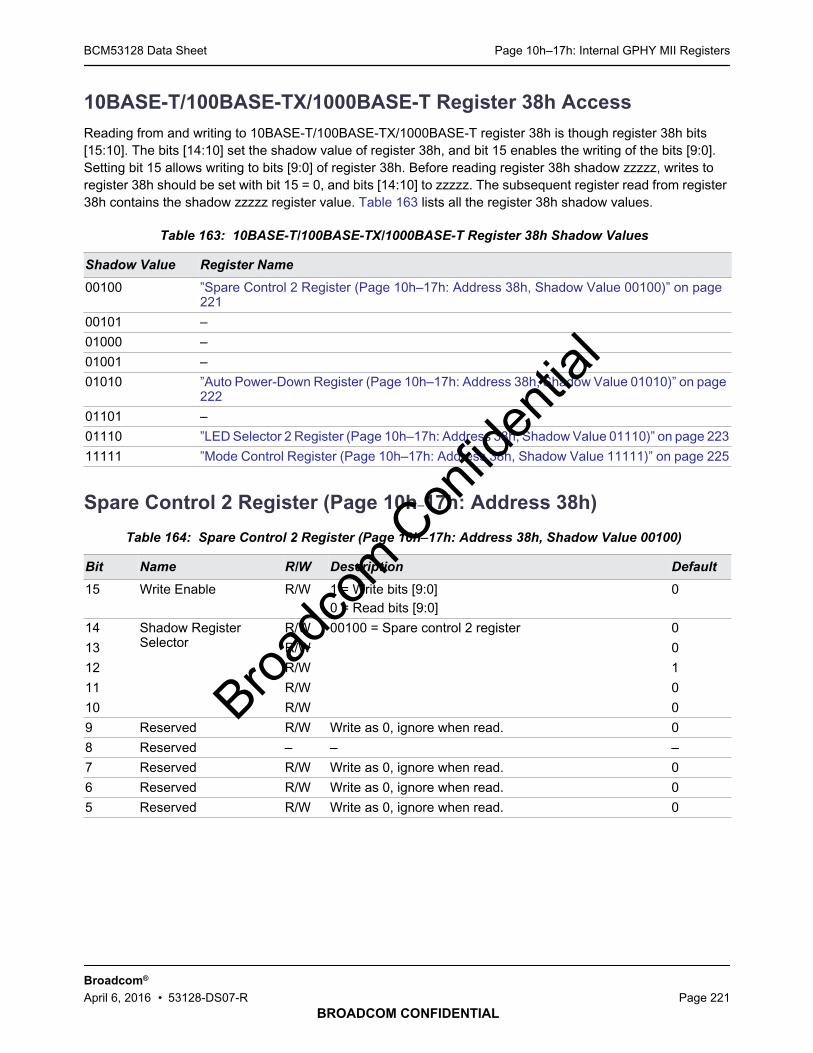
Page 10h–17h: Internal GPHY MII RegistersBCM53128 Data Sheet
BROADCOM CONFIDENTIAL
Broadcom®
April 6, 2016 • 53128-DS07-R Page 221
10BASE-T/100BASE-TX/1000BASE-T Register 38h Access
Reading from and writing to 10BASE-T/100BASE-TX/1000BASE-T register 38h is though register 38h bits[15:10]. The bits [14:10] set the shadow value of register 38h, and bit 15 enables the writing of the bits [9:0].Setting bit 15 allows writing to bits [9:0] of register 38h. Before reading register 38h shadow zzzzz, writes toregister 38h should be set with bit 15 = 0, and bits [14:10] to zzzzz. The subsequent register read from register38h contains the shadow zzzzz register value. Table 163 lists all the register 38h shadow values.
Spare Control 2 Register (Page 10h–17h: Address 38h)
Table 163: 10BASE-T/100BASE-TX/1000BASE-T Register 38h Shadow Values
Shadow Value Register Name
00100 ”Spare Control 2 Register (Page 10h–17h: Address 38h, Shadow Value 00100)” on page221
00101 –
01000 –
01001 –
01010 ”Auto Power-Down Register (Page 10h–17h: Address 38h, Shadow Value 01010)” on page222
01101 –
01110 ”LED Selector 2 Register (Page 10h–17h: Address 38h, Shadow Value 01110)” on page 223
11111 ”Mode Control Register (Page 10h–17h: Address 38h, Shadow Value 11111)” on page 225
Table 164: Spare Control 2 Register (Page 10h–17h: Address 38h, Shadow Value 00100)
Bit Name R/W Description Default
15 Write Enable R/W 1 = Write bits [9:0]0 = Read bits [9:0]
0
14 Shadow RegisterSelector
R/W 00100 = Spare control 2 register 0
13 R/W 0
12 R/W 1
11 R/W 0
10 R/W 0
9 Reserved R/W Write as 0, ignore when read. 0
8 Reserved – – –
7 Reserved R/W Write as 0, ignore when read. 0
6 Reserved R/W Write as 0, ignore when read. 0
5 Reserved R/W Write as 0, ignore when read. 0
Broadc
om C
onfid
entia
l

Page 10h–17h: Internal GPHY MII RegistersBCM53128 Data Sheet
BROADCOM CONFIDENTIAL
Broadcom®
April 6, 2016 • 53128-DS07-R Page 222
Auto Power-Down Register (Page 10h–17h: Address 38h)
4 Ethernet@WireSpeedRetry Limit
RO 000 = Downgrade after 2 failed auto-negotiation attempts.001 = Downgrade after 3 failed auto-negotiation attempts.010 = Downgrade after 4 failed auto-negotiation attempts.011 = Downgrade after 5 failed auto-negotiation attempts.100 = Downgrade after 6 failed auto-negotiation attempts.101 = Downgrade after 7 failed auto-negotiation attempts.110 = Downgrade after 8 failed auto-negotiation attempts.111 = Downgrade after 9 failed auto-negotiation attempts.
0
3 1
2 1
1 Energy Detect on INTRLED Pin
R/W 1 = Routes energy detect to interrupt signal. Use LEDselectors (register 38h shadow 01101 and 01110) andprogram to INTR mode.0 = INTR LED pin performs the Interrupt function.
0
0 Reserved R/W Write as 0, ignore when read. 0
Table 165: Auto Power-Down Register (Page 10h–17h: Address 38h, Shadow Value 01010)
Bit Name R/W Description Default
15 Write Enable R/W 1 = Write bits [9:0]0 = Read bits [9:0]
0
14 Shadow Register Selector R/W 01010 = Auto power-down register 0
13 R/W 1
12 R/W 0
11 R/W 1
10 R/W 0
9 Reserved R/W Write as 0, ignore when read. 0
8 Reserved R/W Write as 0, ignore when read. 0
7 Reserved R/W Write as 0, ignore when read. 0
6 Reserved R/W Write as 0, ignore when read. 0
5 Auto Power-Down Mode R/W 1 = Auto power-down mode is enabled.0 = Auto power-down mode is disabled.
0
4 Sleep Timer Select R/W 1 = Sleep timer is 5.4 seconds.0 = Sleep timer is 2.7 seconds.
0
3 Wake-up Timer Select R/W Counter for wake-up timer in units of 84 ms0001 = 84 ms0010 = 168 ms...1111 = 1.26 sec.
0
2 R/W 0
1 R/W 0
0 R/W 1
Table 164: Spare Control 2 Register (Page 10h–17h: Address 38h, Shadow Value 00100) (Cont.)
Bit Name R/W Description Default
Broadc
om C
onfid
entia
l

Page 10h–17h: Internal GPHY MII RegistersBCM53128 Data Sheet
BROADCOM CONFIDENTIAL
Broadcom®
April 6, 2016 • 53128-DS07-R Page 223
LED Selector 2 Register (Page 10h–17h: Address 38h)
Table 166: LED Selector 2 Register (Page 10h–17h: Address 38h, Shadow Value 01110)
Bit Name R/W Description Default
15 Write Enable R/W 1 = Write bits [9:0]0 = Read bits [9:0]
0
14 Shadow Register Selector R/W 01110 = LED status register 0
13 R/W 1
12 R/W 1
11 R/W 1
10 R/W 0
9 Reserved R/W Write as 0, ignore when read. 0
8 Reserved R/W Write as 0, ignore when read. 0
7 LED4 Selector R/W 0000 = LINKSPD[1]0001 = LINKSPD[2]0010 = XMITLED0011 = ACTIVITY0100 = FDXLED0101 = SLAVE0110 = INTR0111 = QUALITY1000 = RCVLED1001 = WIRESPD_DOWNGRADE1010 = MULTICOLOR[2]1011 = CABLE DIAGNOSTIC OPEN/SHORT1100 = RESERVED1101 = CRS (SGMII mode)1110 = Off (high)1111 = On (low)
0
6 R/W 1
5 R/W 1
4 R/W 0
Broadc
om C
onfid
entia
l
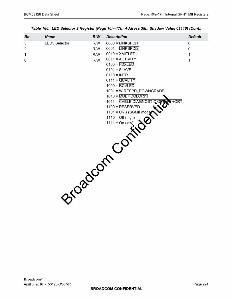
Page 10h–17h: Internal GPHY MII RegistersBCM53128 Data Sheet
BROADCOM CONFIDENTIAL
Broadcom®
April 6, 2016 • 53128-DS07-R Page 224
3 LED3 Selector R/W 0000 = LINKSPD[1]0001 = LINKSPD[2]0010 = XMITLED0011 = ACTIVITY0100 = FDXLED0101 = SLAVE0110 = INTR0111 = QUALITY1000 = RCVLED1001 = WIRESPD_DOWNGRADE1010 = MULTICOLOR[1]1011 = CABLE DIAGNOSTIC OPEN/SHORT1100 = RESERVED1101 = CRS (SGMII mode)1110 = Off (high)1111 = On (low)
0
2 R/W 0
1 R/W 1
0 R/W 1
Table 166: LED Selector 2 Register (Page 10h–17h: Address 38h, Shadow Value 01110) (Cont.)
Bit Name R/W Description Default
Broadc
om C
onfid
entia
l
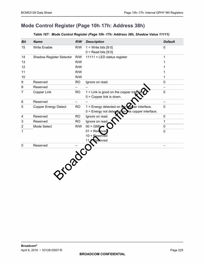
Page 10h–17h: Internal GPHY MII RegistersBCM53128 Data Sheet
BROADCOM CONFIDENTIAL
Broadcom®
April 6, 2016 • 53128-DS07-R Page 225
Mode Control Register (Page 10h–17h: Address 38h)
Table 167: Mode Control Register (Page 10h–17h: Address 38h, Shadow Value 11111)
Bit Name R/W Description Default
15 Write Enable R/W 1 = Write bits [9:0]0 = Read bits [9:0]
0
14 Shadow Register Selector R/W 11111 = LED status register 1
13 R/W 1
12 R/W 1
11 R/W 1
10 R/W 1
9 Reserved RO Ignore on read. 0
8 Reserved – – –
7 Copper Link RO 1 = Link is good on the copper interface.0 = Copper link is down.
0
6 Reserved – – –
5 Copper Energy Detect RO 1 = Energy detected on the copper interface.0 = Energy not detected on the copper interface.
0
4 Reserved RO Ignore on read. 0
3 Reserved RO Ignore on read. 1
2 Mode Select R/W 00 = GMII01 = Reserved10 = Reserved11 = Reserved
0
1 0
0 Reserved – – –
Broadc
om C
onfid
entia
l
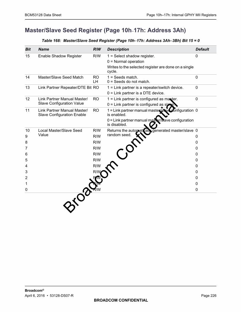
Page 10h–17h: Internal GPHY MII RegistersBCM53128 Data Sheet
BROADCOM CONFIDENTIAL
Broadcom®
April 6, 2016 • 53128-DS07-R Page 226
Master/Slave Seed Register (Page 10h–17h: Address 3Ah)
Table 168: Master/Slave Seed Register (Page 10h–17h: Address 3Ah–3Bh) Bit 15 = 0
Bit Name R/W Description Default
15 Enable Shadow Register R/W 1 = Select shadow register.0 = Normal operationWrites to the selected register are done on a singlecycle.
0
14 Master/Slave Seed Match ROLH
1 = Seeds match.0 = Seeds do not match.
0
13 Link Partner Repeater/DTE Bit RO 1 = Link partner is a repeater/switch device.0 = Link partner is a DTE device.
0
12 Link Partner Manual Master/Slave Configuration Value
RO 1 = Link partner is configured as master.0 = Link partner is configured as slave.
0
11 Link Partner Manual Master/Slave Configuration Enable
RO 1 = Link partner manual master/slave configurationis enabled.0 = Link partner manual master/slave configurationis disabled.
0
10 Local Master/Slave SeedValue
R/W Returns the automatically generated master/slaverandom seed.
0
9 R/W 0
8 R/W 0
7 R/W 0
6 R/W 0
5 R/W 0
4 R/W 0
3 R/W 0
2 R/W 0
1 R/W 0
0 R/W 0
Broadc
om C
onfid
entia
l
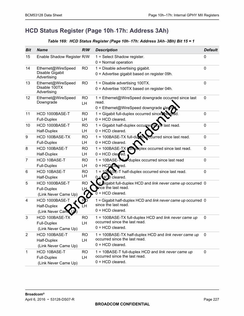
Page 10h–17h: Internal GPHY MII RegistersBCM53128 Data Sheet
BROADCOM CONFIDENTIAL
Broadcom®
April 6, 2016 • 53128-DS07-R Page 227
HCD Status Register (Page 10h–17h: Address 3Ah)
Table 169: HCD Status Register (Page 10h–17h: Address 3Ah–3Bh) Bit 15 = 1
Bit Name R/W Description Default
15 Enable Shadow Register R/W 1 = Select Shadow register.0 = Normal operation
0
14 Ethernet@WireSpeedDisable GigabitAdvertising
RO 1 = Disable advertising gigabit.0 = Advertise gigabit based on register 09h.
0
13 Ethernet@WireSpeedDisable 100TXAdvertising
RO 1 = Disable advertising 100TX.0 = Advertise 100TX based on register 04h.
0
12 Ethernet@WireSpeedDowngrade
ROLH
1 = Ethernet@WireSpeed downgrade occurred since lastread.0 = Ethernet@WireSpeed downgrade cleared.
0
11 HCD 1000BASE-TFull-Duplex
ROLH
1 = Gigabit full-duplex occurred since last read.0 = HCD cleared.
0
10 HCD 1000BASE-THalf-Duplex
ROLH
1 = Gigabit half-duplex occurred since last read.0 = HCD cleared.
0
9 HCD 100BASE-TXFull-Duplex
ROLH
1 = 100BASE-TX full-duplex occurred since last read.0 = HCD cleared.
0
8 HCD 100BASE-THalf-Duplex
ROLH
1 = 100BASE-TX half-duplex occurred since last read.0 = HCD cleared.
0
7 HCD 10BASE-TFull-Duplex
ROLH
1 = 10BASE-T full-duplex occurred since last read0 = HCD cleared.
0
6 HCD 10BASE-THalf-Duplex
ROLH
1 = 10BASE-T half-duplex occurred since last read.0 = HCD cleared.
0
5 HCD 1000BASE-TFull-Duplex(Link Never Came Up)
ROLH
1 = Gigabit full-duplex HCD and link never came up occurredsince the last read.0 = HCD cleared.
0
4 HCD 1000BASE-THalf-Duplex(Link Never Came Up)
ROLH
1 = Gigabit half-duplex HCD and link never came up occurredsince the last read.0 = HCD cleared.
0
3 HCD 100BASE-TXFull-Duplex(Link Never Came Up)
ROLH
1 = 100BASE-TX full-duplex HCD and link never came upoccurred since the last read.0 = HCD cleared.
0
2 HCD 100BASE-THalf-Duplex(Link Never Came Up)
ROLH
1 = 100BASE-TX half-duplex HCD and link never came upoccurred since the last read.0 = HCD cleared.
0
1 HCD 10BASE-TFull-Duplex(Link Never Came Up)
ROLH
1 = 10BASE-T full-duplex HCD and link never came upoccurred since the last read.0 = HCD cleared.
0
Broadc
om C
onfid
entia
l
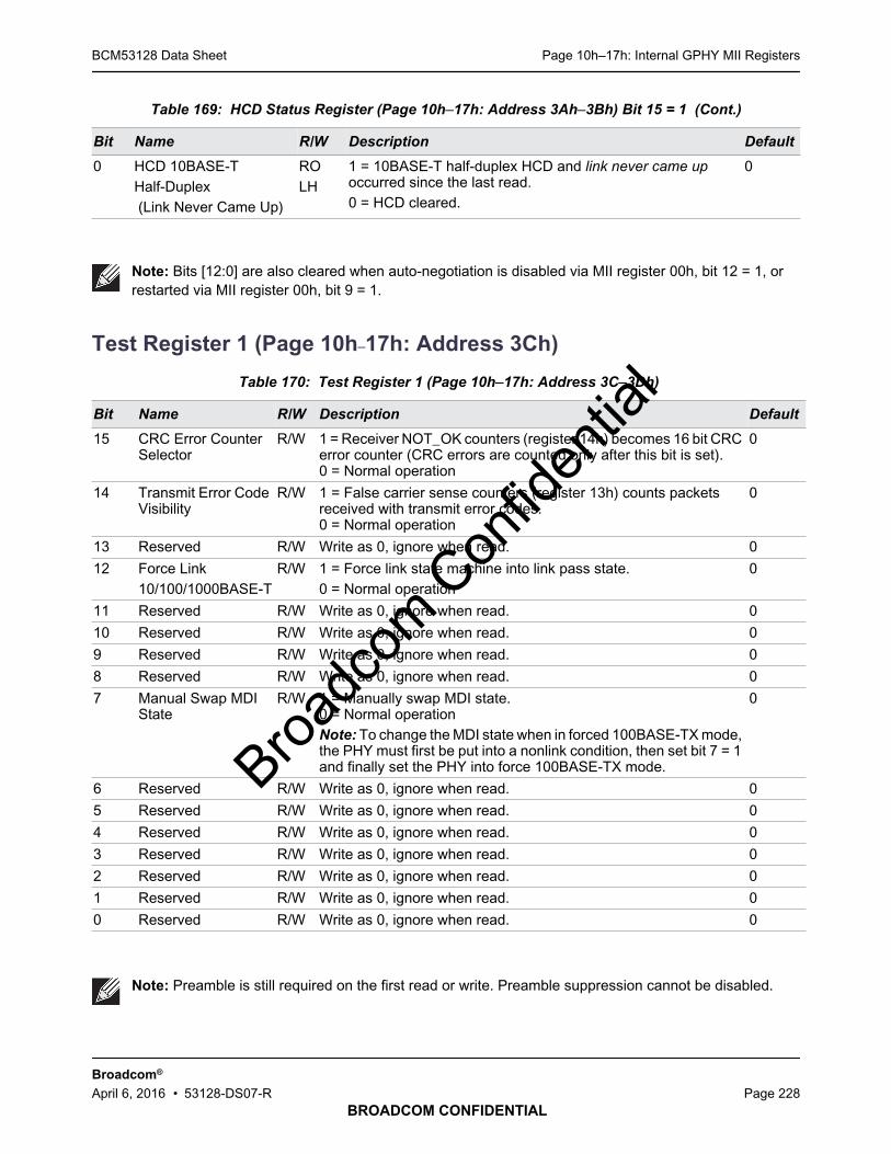
Page 10h–17h: Internal GPHY MII RegistersBCM53128 Data Sheet
BROADCOM CONFIDENTIAL
Broadcom®
April 6, 2016 • 53128-DS07-R Page 228
Test Register 1 (Page 10h–17h: Address 3Ch)
0 HCD 10BASE-THalf-Duplex(Link Never Came Up)
ROLH
1 = 10BASE-T half-duplex HCD and link never came upoccurred since the last read.0 = HCD cleared.
0
Note: Bits [12:0] are also cleared when auto-negotiation is disabled via MII register 00h, bit 12 = 1, orrestarted via MII register 00h, bit 9 = 1.
Table 170: Test Register 1 (Page 10h–17h: Address 3C–3Dh)
Bit Name R/W Description Default
15 CRC Error CounterSelector
R/W 1 = Receiver NOT_OK counters (register 14h) becomes 16 bit CRCerror counter (CRC errors are counted only after this bit is set).0 = Normal operation
0
14 Transmit Error CodeVisibility
R/W 1 = False carrier sense counters (register 13h) counts packetsreceived with transmit error codes.0 = Normal operation
0
13 Reserved R/W Write as 0, ignore when read. 0
12 Force Link10/100/1000BASE-T
R/W 1 = Force link state machine into link pass state.0 = Normal operation
0
11 Reserved R/W Write as 0, ignore when read. 0
10 Reserved R/W Write as 0, ignore when read. 0
9 Reserved R/W Write as 0, ignore when read. 0
8 Reserved R/W Write as 0, ignore when read. 0
7 Manual Swap MDIState
R/W 1 = Manually swap MDI state.0 = Normal operationNote: To change the MDI state when in forced 100BASE-TX mode,the PHY must first be put into a nonlink condition, then set bit 7 = 1and finally set the PHY into force 100BASE-TX mode.
0
6 Reserved R/W Write as 0, ignore when read. 0
5 Reserved R/W Write as 0, ignore when read. 0
4 Reserved R/W Write as 0, ignore when read. 0
3 Reserved R/W Write as 0, ignore when read. 0
2 Reserved R/W Write as 0, ignore when read. 0
1 Reserved R/W Write as 0, ignore when read. 0
0 Reserved R/W Write as 0, ignore when read. 0
Note: Preamble is still required on the first read or write. Preamble suppression cannot be disabled.
Table 169: HCD Status Register (Page 10h–17h: Address 3Ah–3Bh) Bit 15 = 1 (Cont.)
Bit Name R/W Description Default
Broadc
om C
onfid
entia
l

Expansion RegistersBCM53128 Data Sheet
BROADCOM CONFIDENTIAL
Broadcom®
April 6, 2016 • 53128-DS07-R Page 229
Expansion Registers
Expansion Register 00h: Receive/Transmit Packet Counter
Expansion register 00h is enabled by writing to “Expansion Register Access Register (Page 10h–17h: Address2Eh–2Fh)” bits [11:0] = ‘F00’h, and read/write access is through register 2Ah.
Packet Counter (Copper Only)
The mode of this counter is set by bit 11 of “Miscellaneous Control Register (Page 10h–17h: Address 30h,Shadow Value 111)”. When bit 11 =1, then receive packets (both good and bad CRC error packets) are counted.When bit 11 = 0, then transmit packets (both good and bad CRC error packets) are counted. This counter iscleared on read and freezes at FFFFh.
Expansion Register 01h: Expansion Interrupt Status
Expansion register 00h is enabled by writing to “Expansion Register Access Register (Page 10h–17h: Address2Eh–2Fh)” bits [11:0] = ‘F01’h, and read/write access is through register 2Ah.
Transmit CRC Error
This bit indicates that a transmit CRC error has been detected since the last read.
Table 171: Expansion Register 00h: Receive/Transmit Packet Counter
Bit Name R/W Description Default
15:0 Packet Counter(Copper Only)
R/WCR
Returns the transmitted and received packet count. 0000h
Table 172: Expansion Register 01h: Expansion Interrupt Status
Bit Name R/W Description Default
15:1 Reserved RO Write as 0, ignore on read 0
0 Transmit CRC Error ROLH
1 = Transmit CRC error detected since last read.0 = No transmit CRC error detected.
0
Broadc
om C
onfid
entia
l
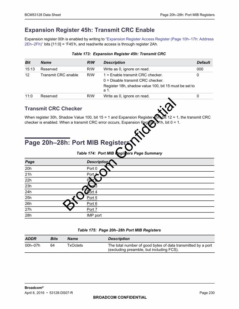
Page 20h–28h: Port MIB RegistersBCM53128 Data Sheet
BROADCOM CONFIDENTIAL
Broadcom®
April 6, 2016 • 53128-DS07-R Page 230
Expansion Register 45h: Transmit CRC Enable
Expansion register 00h is enabled by writing to “Expansion Register Access Register (Page 10h–17h: Address2Eh–2Fh)” bits [11:0] = ‘F45’h, and read/write access is through register 2Ah.
Transmit CRC Checker
When register 30h, Shadow Value 100, bit 15 = 1 and Expansion Register 45h, bit 12 = 1, the transmit CRCchecker is enabled. When a transmit CRC error occurs, Expansion Register 01h, bit 0 = 1.
Page 20h–28h: Port MIB Registers
Table 173: Expansion Register 45h: Transmit CRC
Bit Name R/W Description Default
15:13 Reserved R/W Write as 0, ignore on read. 000
12 Transmit CRC enable R/W 1 = Enable transmit CRC checker.0 = Disable transmit CRC checker.Register 18h, shadow value 100, bit 15 must be set toa 1.
0
11:0 Reserved R/W Write as 0, ignore on read. 0
Table 174: Port MIB Registers Page Summary
Page Description
20h Port 0
21h Port 1
22h Port 2
23h Port 3
24h Port 4
25h Port 5
26h Port 6
27h Port 7
28h IMP port
Table 175: Page 20h–28h Port MIB Registers
ADDR Bits Name Description
00h–07h 64 TxOctets The total number of good bytes of data transmitted by a port(excluding preamble, but including FCS).
Broadc
om C
onfid
entia
l

Page 20h–28h: Port MIB RegistersBCM53128 Data Sheet
BROADCOM CONFIDENTIAL
Broadcom®
April 6, 2016 • 53128-DS07-R Page 231
08h–0Bh 32 TxDropPkts This counter is incremented every time a transmit packet isdropped due to lack of resources (e.g., transmit FIFOunderflow), or an internal MAC sublayer transmit error notcounted by either the TxLateCollision or theTxExcessiveCollision counters.
0Ch–0Fh 32 TxQ0PKT The total number of good packets transmitted on COS0, whichis specified in MIB queue select register when QoS is enabled.
10h–13h 32 TxBroadcastPkts The number of good packets transmitted by a port that aredirected to a broadcast address. This counter does not includeerrored broadcast packets or valid multicast packets.
14h–17h 32 TxMulticastPkts The number of good packets transmitted by a port that aredirected to a multicast address. This counter does not includeerrored multicast packets or valid broadcast packets.
18h–1Bh 32 TxUnicastPkts The number of good packets transmitted by a port that areaddressed to a unicast address.
1Ch–1Fh 32 TxCollisions The number of collisions experienced by a port during packettransmissions.
20h–23h 32 TxSingleCollision The number of packets successfully transmitted by a port thatexperienced exactly one collision.
24h–27h 32 TxMultiple Collision The number of packets successfully transmitted by a port thatexperienced more than one collision.
28h–2Bh 32 TxDeferredTransmit The number of packets transmitted by a port for which the firsttransmission attempt is delayed because the medium is busy.
2Ch–2Fh 32 TxLateCollision The number of times that a collision is detected later than 512bit-times into the transmission of a packet.
30h–33h 32 TxExcessiveCollision The number of packets that are not transmitted from a portbecause the packet experienced 16 transmission attempts.
34h–37h 32 TxFrameInDisc The number of valid packets received that are discarded bythe forwarding process due to lack of space on an outputqueue. (Not maintained or reported in the MIB counters andlocated in the congestion management registers [Page 0Ah].)This attribute only increments if a network device is not actingin compliance with a flow-control request, or the BCM53128internal flow control/buffering scheme has beenmisconfigured.
38h–3Bh 32 TxPausePkts The number of PAUSE events on a given port.
3Ch–3Fh 32 TxQ1PKT The total number of good packets transmitted on COS1, whichisspecified inMIBqueueselect registerwhenQoSisenabled.
40h–43h 32 TxQ2PKT The total number of good packets transmitted on COS2, whichis specified in MIB queue select register when QoS is enabled.
44h–47h 32 TxQ3PKT The total number of good packets transmitted on COS3, whichis specified in MIB queue select register when QoS is enabled.
48h–4Bh 32 TxQ4PKT The total number of good packets transmitted on COS4, whichis specified in MIB queue select register when QoS is enabled.
4Ch–4Fh 32 TxQ5PKT The total number of good packets transmitted on COS5, whichis specified in MIB queue select register when QoS is enabled.
Table 175: Page 20h–28h Port MIB Registers (Cont.)
ADDR Bits Name Description
Broadc
om C
onfid
entia
l

Page 20h–28h: Port MIB RegistersBCM53128 Data Sheet
BROADCOM CONFIDENTIAL
Broadcom®
April 6, 2016 • 53128-DS07-R Page 232
50h–57h 64 RxOctets The number of bytes of data received by a port (excludingpreamble, but including FCS), including bad packets.
58h–5Bh 32 RxUndersizePkts The number of good packets received by a port that are lessthan 64 bytes long (excluding framing bits, but including theFCS).
5Ch–5Fh 32 RxPausePkts The number of PAUSE frames received by a port. The PAUSEframe must have a valid MAC control frame EtherType field(88–08h), have a destination MAC address of either the MACcontrol frame reserved multicast address (01-80-C2-00-00-01) or the unique MAC address associated with the specificport, a valid PAUSE Opcode (00–01), be a minimum of 64bytes in length (excluding preamble but including FCS), andhave a valid CRC. Although an IEEE 802.3-compliant MAC isonly permitted to transmit PAUSE frames when in full-duplexmode with flow control enabled and with the transfer ofPAUSE frames determined by the result of auto-negotiation,an IEEE 802.3 MAC receiver is required to count all receivedPAUSE frames, regardless of its half/full-duplex status. Anindication that a MAC is in half-duplex with the RxPausePktsincrementing indicates a noncompliant transmitting device onthe network.
60h–63h 32 Pkts64Octets The number of packets (including error packets) that are 64bytes long.
64h–67h 32 Pkts65to127Octets The number of packets (including error packets) that arebetween 65 and 127 bytes long.
68h–6Bh 32 Pkts128to255Octets The number of packets (including error packets) that arebetween 128 and 255 bytes long.
6Ch–6Fh 32 Pkts256to511Octets The number of packets (including error packets) that arebetween 256 and 511 bytes long.
70h–73h 32 Pkts512to1023Octets The number of packets (including error packets) that arebetween 512 and 1023 bytes long.
74h–77h 32 Pkts1024toMaxPktOctets
The number of packets (including error packets) that arebetween 1024 and MaxPacket bytes long.
78h–7Bh 32 RxOversizePkts The number of good packets received by a port that aregreater than standard max frame size.
7Ch–7Fh 32 RxJabbers The number of packets received by a port that are longer than1522 bytes and have either an FCS error or an alignmenterror.
80h–83h 32 RxAlignmentErrors The number of packets received by a port that have a length(excluding framing bits, but including FCS) between 64 andstandard max frame size, inclusive, and have a bad FCS witha nonintegral number of bytes.
84h–87h 32 RxFCSErrors The number of packets received by a port that have a length(excluding framing bits, but including FCS) between 64 andstandard max frame size, inclusive, and have a bad FCS withan integral number of bytes.
88h–8Fh 64 RxGoodOctets The total number of bytes in all good packets received by aport (excluding framing bits but including FCS).
Table 175: Page 20h–28h Port MIB Registers (Cont.)
ADDR Bits Name Description
Broadc
om C
onfid
entia
l

Page 20h–28h: Port MIB RegistersBCM53128 Data Sheet
BROADCOM CONFIDENTIAL
Broadcom®
April 6, 2016 • 53128-DS07-R Page 233
90h–93h 32 RxDropPkts The number of good packets received by a port that weredropped due to lack of resources (e.g., lack of input buffers) orwere dropped due to lack of resources before a determinationof the validity of the packet was able to be made (e.g., receiveFIFO overflow). The counter is only incremented if the receiveerror was not counted by the RxAlignmentErrors or theRxFCSErrors counters.
94h–97h 32 RxUnicastPkts The number of good packets received by a port that areaddressed to a unicast address.
98h–9Bh 32 RxMulticastPkts The number of good packets received by a port that aredirected to a multicast address. This counter does not includeerrored multicast packets or valid broadcast packets.
9Ch–9Fh 32 RxBroadcastPkts The number of good packets received by a port that aredirected to the broadcast address. This counter does notinclude errored broadcast packets or valid multicast packets.
A0h–A3h 32 RxSAChanges The number of times the SA of good receive packets haschanged from the previous value. A count greater than 1generally indicates the port is connected to a repeater-basednetwork.
A4h–A7h 32 RxFragments The number of packets received by a port that are less than 64bytes (excluding framing bits) and have either an FCS error oran alignment error.
A8h–ABh 32 JumboPkt The number of frames received with frame size greater thanthe Standard Maximum Size and less than or equal to theJumbo Frame Size, regardless of CRC or Alignment errors.Note: InFrame count should count "the JumboPkt count withgood CRC."
ACh–AFh 32 RXSymbolError The total number of times a valid length packet was receivedat a port and at least one invalid data symbol was detected.Counter only increments once per carrier event and does notincrement on detection of collision during the carrier event.
B0h–B3h 32 InRangeErrors The number of frames received with good CRC and thefollowing conditions.The value of Length/Type field is between 46 and 1500inclusive, and does not match the number or (MAC Client Data+ PAD) data octets received,ORThe value of Length/Type field is less than 46, and the numberof data octets received is greater than 46 (which does notrequire padding).
B4h–B7h 32 OutOfRangeErrors The number of frames received with good CRC and the valueof Length/Type field is greater than 1500 and less than 1536.
B8h-BBh 32 EEE Low-Power IdleEvent
In asymmetric mode, this is simply a count of the number oftimes that the lowPowerAssert control signal has beenasserted for each MAC. In symmetric mode, this is the countof the number of times both lowPowerAssert and thelowPowerIndicate (from the receive path) are assertedsimultaneously.
Table 175: Page 20h–28h Port MIB Registers (Cont.)
ADDR Bits Name Description
Broadc
om C
onfid
entia
l

Page 20h–28h: Port MIB RegistersBCM53128 Data Sheet
BROADCOM CONFIDENTIAL
Broadcom®
April 6, 2016 • 53128-DS07-R Page 234
BCh-BFh 32 EEE Low-PowerDuration
This counter accumulates the number of microseconds thatthe associated MAC/PHY is in the low-power idle state. Theunit is 1 used.
C0h–C3h 32 RxDiscard The number of good packets received by a port that werediscarded by the Forwarding Process.
F0h–F7h 64 “SPI Data I/O Register(Global, Address F0h)”on page 295, bytes 0–7
–
F8h–FDh – Reserved –
FEh 8 “SPI Status Register(Global, Address FEh)”on page 295
–
FFh 8 “Page Register(Global, Address FFh)”on page 296
–
Table 175: Page 20h–28h Port MIB Registers (Cont.)
ADDR Bits Name Description
Broadc
om C
onfid
entia
l
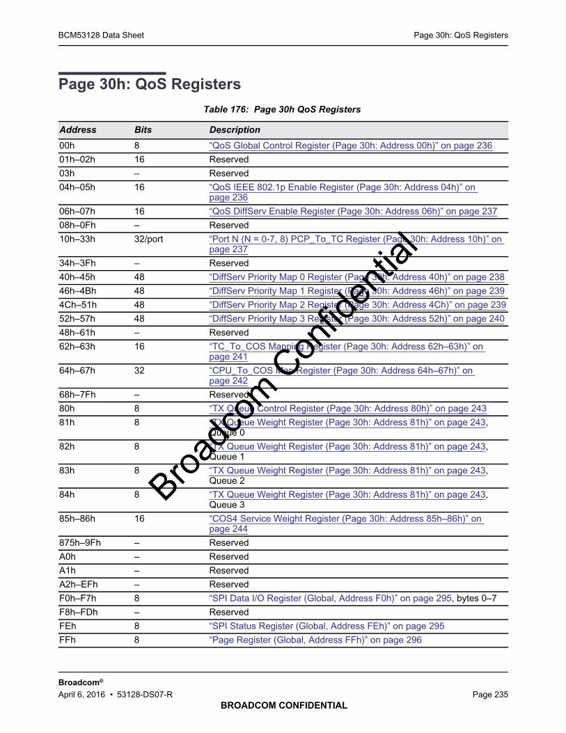
Page 30h: QoS RegistersBCM53128 Data Sheet
BROADCOM CONFIDENTIAL
Broadcom®
April 6, 2016 • 53128-DS07-R Page 235
Page 30h: QoS Registers
Table 176: Page 30h QoS Registers
Address Bits Description
00h 8 “QoS Global Control Register (Page 30h: Address 00h)” on page 236
01h–02h 16 Reserved
03h – Reserved
04h–05h 16 “QoS IEEE 802.1p Enable Register (Page 30h: Address 04h)” onpage 236
06h–07h 16 “QoS DiffServ Enable Register (Page 30h: Address 06h)” on page 237
08h–0Fh – Reserved
10h–33h 32/port “Port N (N = 0-7, 8) PCP_To_TC Register (Page 30h: Address 10h)” onpage 237
34h–3Fh – Reserved
40h–45h 48 “DiffServ Priority Map 0 Register (Page 30h: Address 40h)” on page 238
46h–4Bh 48 “DiffServ Priority Map 1 Register (Page 30h: Address 46h)” on page 239
4Ch–51h 48 “DiffServ Priority Map 2 Register (Page 30h: Address 4Ch)” on page 239
52h–57h 48 “DiffServ Priority Map 3 Register (Page 30h: Address 52h)” on page 240
48h–61h – Reserved
62h–63h 16 “TC_To_COS Mapping Register (Page 30h: Address 62h–63h)” onpage 241
64h–67h 32 “CPU_To_COS Map Register (Page 30h: Address 64h–67h)” onpage 242
68h–7Fh – Reserved
80h 8 “TX Queue Control Register (Page 30h: Address 80h)” on page 243
81h 8 “TX Queue Weight Register (Page 30h: Address 81h)” on page 243,Queue 0
82h 8 “TX Queue Weight Register (Page 30h: Address 81h)” on page 243,Queue 1
83h 8 “TX Queue Weight Register (Page 30h: Address 81h)” on page 243,Queue 2
84h 8 “TX Queue Weight Register (Page 30h: Address 81h)” on page 243,Queue 3
85h–86h 16 “COS4 Service Weight Register (Page 30h: Address 85h–86h)” onpage 244
875h–9Fh – Reserved
A0h – Reserved
A1h – Reserved
A2h–EFh – Reserved
F0h–F7h 8 “SPI Data I/O Register (Global, Address F0h)” on page 295, bytes 0–7
F8h–FDh – Reserved
FEh 8 “SPI Status Register (Global, Address FEh)” on page 295
FFh 8 “Page Register (Global, Address FFh)” on page 296
Broadc
om C
onfid
entia
l
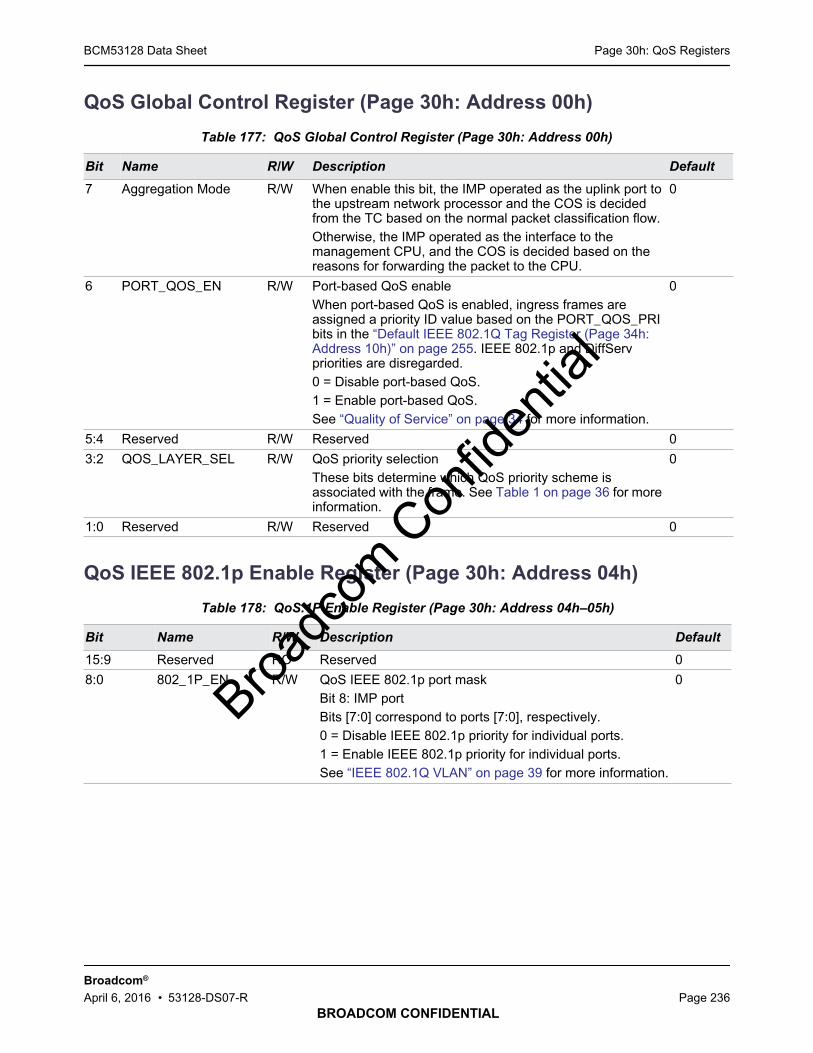
Page 30h: QoS RegistersBCM53128 Data Sheet
BROADCOM CONFIDENTIAL
Broadcom®
April 6, 2016 • 53128-DS07-R Page 236
QoS Global Control Register (Page 30h: Address 00h)
QoS IEEE 802.1p Enable Register (Page 30h: Address 04h)
Table 177: QoS Global Control Register (Page 30h: Address 00h)
Bit Name R/W Description Default
7 Aggregation Mode R/W When enable this bit, the IMP operated as the uplink port tothe upstream network processor and the COS is decidedfrom the TC based on the normal packet classification flow.Otherwise, the IMP operated as the interface to themanagement CPU, and the COS is decided based on thereasons for forwarding the packet to the CPU.
0
6 PORT_QOS_EN R/W Port-based QoS enableWhen port-based QoS is enabled, ingress frames areassigned a priority ID value based on the PORT_QOS_PRIbits in the “Default IEEE 802.1Q Tag Register (Page 34h:Address 10h)” on page 255. IEEE 802.1p and DiffServpriorities are disregarded.0 = Disable port-based QoS.1 = Enable port-based QoS.See “Quality of Service” on page 34 for more information.
0
5:4 Reserved R/W Reserved 0
3:2 QOS_LAYER_SEL R/W QoS priority selectionThese bits determine which QoS priority scheme isassociated with the frame. See Table 1 on page 36 for moreinformation.
0
1:0 Reserved R/W Reserved 0
Table 178: QoS.1P Enable Register (Page 30h: Address 04h–05h)
Bit Name R/W Description Default
15:9 Reserved RO Reserved 0
8:0 802_1P_EN R/W QoS IEEE 802.1p port maskBit 8: IMP portBits [7:0] correspond to ports [7:0], respectively.0 = Disable IEEE 802.1p priority for individual ports.1 = Enable IEEE 802.1p priority for individual ports.See “IEEE 802.1Q VLAN” on page 39 for more information.
0
Broadc
om C
onfid
entia
l

Page 30h: QoS RegistersBCM53128 Data Sheet
BROADCOM CONFIDENTIAL
Broadcom®
April 6, 2016 • 53128-DS07-R Page 237
QoS DiffServ Enable Register (Page 30h: Address 06h)
See “Quality of Service” on page 34 for more information.
Port N (N = 0-7, 8) PCP_To_TC Register (Page 30h: Address 10h).
These bits map the IEEE 802.1p priority level to one of the eight priority ID levels in the “TC_To_COS MappingRegister (Page 30h: Address 62h–63h)” on page 241.
Table 179: QoS DiffServ Enable Register (Page 30h: Address 06h–07h)
Bit Name R/W Description Default
15:9 Reserved RO Reserved 0
8:0 DIFFSERV_EN R/W DiffServ port maskBit 8: IMP portBits [7:0] correspond to ports [7:0], respectively.0 = Disable DiffServ priority for individual ports.1 = Enable DiffServ priority for individual ports.
0
Table 180: Port N (N=0-7,8) PCP_To_TC Register Address Summary
Address Description
10h–13h Port 0
14h–17h Port 1
18h–1Bh Port 2
1Ch–1Fh Port 3
20h–23h Port 4
24h–27h Port 5
28h–2Bh Port 6
2Ch–2Fh Port 7
30h–33h IMP Port
Table 181: Port N (N=0-7,8) PCP_To_TC Register (Page 30h: Address 10h–33h)
BIt Name R/W Description Default
31:24 Reserved RO Reserved 0
23:21 1P_111_MAP R/W IEEE 802.1p priority tag field 111 111
20:18 1P_110_MAP R/W IEEE 802.1p priority tag field 110 110
17:15 1P_101_MAP R/W IEEE 802.1p priority tag field 101 101
14:12 1P_100_MAP R/W IEEE 802.1p priority tag field 100 100
11:9 1P_011_MAP R/W IEEE 802.1p priority tag field 011 011
8:6 1P_010_MAP R/W IEEE 802.1p priority tag field 010 010
5:3 1P_001_MAP R/W IEEE 802.1p priority tag field 001 001
2:0 1P_000_MAP R/W IEEE 802.1p priority tag field 000 000
Broadc
om C
onfid
entia
l
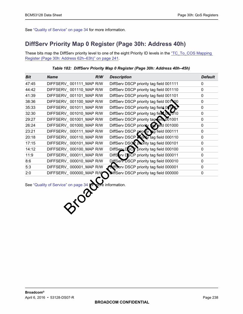
Page 30h: QoS RegistersBCM53128 Data Sheet
BROADCOM CONFIDENTIAL
Broadcom®
April 6, 2016 • 53128-DS07-R Page 238
See “Quality of Service” on page 34 for more information.
DiffServ Priority Map 0 Register (Page 30h: Address 40h)
These bits map the DiffServ priority level to one of the eight Priority ID levels in the “TC_To_COS MappingRegister (Page 30h: Address 62h–63h)” on page 241.
See “Quality of Service” on page 34 for more information.
Table 182: DiffServ Priority Map 0 Register (Page 30h: Address 40h–45h)
Bit Name R/W Description Default
47:45 DIFFSERV_ 001111_MAP R/W DiffServ DSCP priority tag field 001111 0
44:42 DIFFSERV_ 001110_MAP R/W DiffServ DSCP priority tag field 001110 0
41:39 DIFFSERV_ 001101_MAP R/W DiffServ DSCP priority tag field 001101 0
38:36 DIFFSERV_ 001100_MAP R/W DiffServ DSCP priority tag field 001100 0
35:33 DIFFSERV_ 001011_MAP R/W DiffServ DSCP priority tag field 001011 0
32:30 DIFFSERV_ 001010_MAP R/W DiffServ DSCP priority tag field 001010 0
29:27 DIFFSERV_ 001001_MAP R/W DiffServ DSCP priority tag field 001001 0
26:24 DIFFSERV_ 001000_MAP R/W DiffServ DSCP priority tag field 001000 0
23:21 DIFFSERV_ 000111_MAP R/W DiffServ DSCP priority tag field 000111 0
20:18 DIFFSERV_ 000110_MAP R/W DiffServ DSCP priority tag field 000110 0
17:15 DIFFSERV_ 000101_MAP R/W DiffServ DSCP priority tag field 000101 0
14:12 DIFFSERV_ 000100_MAP R/W DiffServ DSCP priority tag field 000100 0
11:9 DIFFSERV_ 000011_MAP R/W DiffServ DSCP priority tag field 000011 0
8:6 DIFFSERV_ 000010_MAP R/W DiffServ DSCP priority tag field 000010 0
5:3 DIFFSERV_ 000001_MAP R/W DiffServ DSCP priority tag field 000001 0
2:0 DIFFSERV_ 000000_MAP R/W DiffServ DSCP priority tag field 000000 0
Broadc
om C
onfid
entia
l

Page 30h: QoS RegistersBCM53128 Data Sheet
BROADCOM CONFIDENTIAL
Broadcom®
April 6, 2016 • 53128-DS07-R Page 239
DiffServ Priority Map 1 Register (Page 30h: Address 46h)
These bits map the DiffServ priority level to one of the eight Priority ID levels in the “TC_To_COS MappingRegister (Page 30h: Address 62h–63h)” on page 241.
See “Quality of Service” on page 34 for more information.
DiffServ Priority Map 2 Register (Page 30h: Address 4Ch)
These bits map the DiffServ priority level to one of the eight priority ID levels in the “TC_To_COS MappingRegister (Page 30h: Address 62h–63h)” on page 241.
Table 183: DiffServ Priority Map 1 Register (Page 30h: Address 46h–4Bh)
Bit Name R/W Description Default
47:45 DIFFSERV_ 011111_MAP R/W DiffServ DSCP priority tag field 011111 0
44:42 DIFFSERV_ 011110_MAP R/W DiffServ DSCP priority tag field 011110 0
41:39 DIFFSERV_ 011101_MAP R/W DiffServ DSCP priority tag field 011101 0
38:36 DIFFSERV_ 011100_MAP R/W DiffServ DSCP priority tag field 011100 0
35:33 DIFFSERV_ 011011_MAP R/W DiffServ DSCP priority tag field 011011 0
32:30 DIFFSERV_ 011010_MAP R/W DiffServ DSCP priority tag field 011010 0
29:27 DIFFSERV_ 011001_MAP R/W DiffServ DSCP priority tag field 011001 0
26:24 DIFFSERV_ 011000_MAP R/W DiffServ DSCP priority tag field 011000 0
23:21 DIFFSERV_ 010111_MAP R/W DiffServ DSCP priority tag field 010111 0
20:18 DIFFSERV_ 010110_MAP R/W DiffServ DSCP priority tag field 010110 0
17:15 DIFFSERV_ 010101_MAP R/W DiffServ DSCP priority tag field 010101 0
14:12 DIFFSERV_ 010100_MAP R/W DiffServ DSCP priority tag field 010100 0
11:9 DIFFSERV_ 010011_MAP R/W DiffServ DSCP priority tag field 010011 0
8:6 DIFFSERV_ 010010_MAP R/W DiffServ DSCP priority tag field 010010 0
5:3 DIFFSERV_ 010001_MAP R/W DiffServ DSCP priority tag field 010001 0
2:0 DIFFSERV_ 010000_MAP R/W DiffServ DSCP priority tag field 010000 0
Table 184: DiffServ Priority Map 2 Register (Page 30h: Address 4Ch–51h)
Bit Name R/W Description Default
47:45 DIFFSERV_ 101111_MAP R/W DiffServ DSCP priority tag field 101111 0
44:42 DIFFSERV_ 101110_MAP R/W DiffServ DSCP priority tag field 101110 0
41:39 DIFFSERV_ 101101_MAP R/W DiffServ DSCP priority tag field 101101 0
38:36 DIFFSERV_ 101100_MAP R/W DiffServ DSCP priority tag field 101100 0
35:33 DIFFSERV_ 101011_MAP R/W DiffServ DSCP priority tag field 101011 0
32:30 DIFFSERV_ 101010_MAP R/W DiffServ DSCP priority tag field 101010 0
29:27 DIFFSERV_ 101001_MAP R/W DiffServ DSCP priority tag field 101001 0
26:24 DIFFSERV_ 101000_MAP R/W DiffServ DSCP priority tag field 101000 0
23:21 DIFFSERV_ 100111_MAP R/W DiffServ DSCP priority tag field 100111 0
Broadc
om C
onfid
entia
l
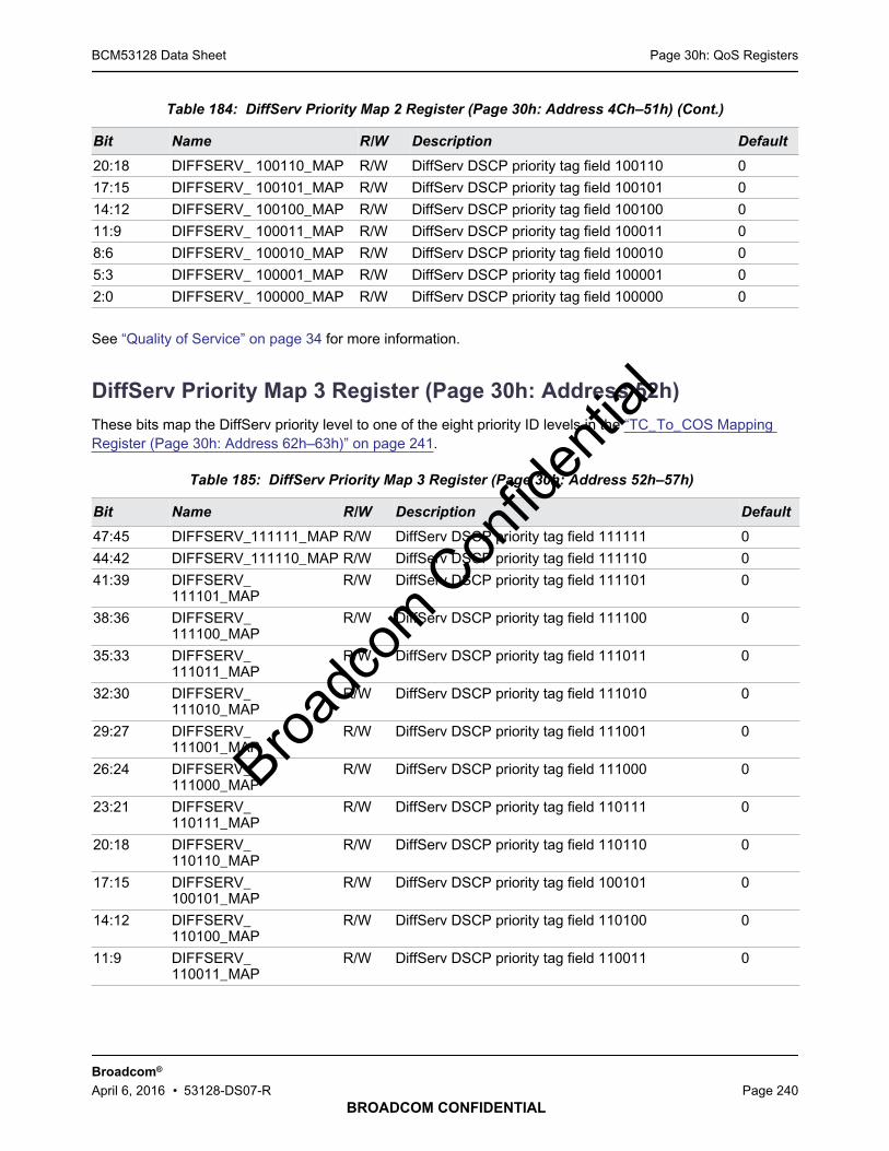
Page 30h: QoS RegistersBCM53128 Data Sheet
BROADCOM CONFIDENTIAL
Broadcom®
April 6, 2016 • 53128-DS07-R Page 240
See “Quality of Service” on page 34 for more information.
DiffServ Priority Map 3 Register (Page 30h: Address 52h)
These bits map the DiffServ priority level to one of the eight priority ID levels in the “TC_To_COS MappingRegister (Page 30h: Address 62h–63h)” on page 241.
20:18 DIFFSERV_ 100110_MAP R/W DiffServ DSCP priority tag field 100110 0
17:15 DIFFSERV_ 100101_MAP R/W DiffServ DSCP priority tag field 100101 0
14:12 DIFFSERV_ 100100_MAP R/W DiffServ DSCP priority tag field 100100 0
11:9 DIFFSERV_ 100011_MAP R/W DiffServ DSCP priority tag field 100011 0
8:6 DIFFSERV_ 100010_MAP R/W DiffServ DSCP priority tag field 100010 0
5:3 DIFFSERV_ 100001_MAP R/W DiffServ DSCP priority tag field 100001 0
2:0 DIFFSERV_ 100000_MAP R/W DiffServ DSCP priority tag field 100000 0
Table 185: DiffServ Priority Map 3 Register (Page 30h: Address 52h–57h)
Bit Name R/W Description Default
47:45 DIFFSERV_111111_MAP R/W DiffServ DSCP priority tag field 111111 0
44:42 DIFFSERV_111110_MAP R/W DiffServ DSCP priority tag field 111110 0
41:39 DIFFSERV_111101_MAP
R/W DiffServ DSCP priority tag field 111101 0
38:36 DIFFSERV_111100_MAP
R/W DiffServ DSCP priority tag field 111100 0
35:33 DIFFSERV_111011_MAP
R/W DiffServ DSCP priority tag field 111011 0
32:30 DIFFSERV_111010_MAP
R/W DiffServ DSCP priority tag field 111010 0
29:27 DIFFSERV_111001_MAP
R/W DiffServ DSCP priority tag field 111001 0
26:24 DIFFSERV_111000_MAP
R/W DiffServ DSCP priority tag field 111000 0
23:21 DIFFSERV_110111_MAP
R/W DiffServ DSCP priority tag field 110111 0
20:18 DIFFSERV_110110_MAP
R/W DiffServ DSCP priority tag field 110110 0
17:15 DIFFSERV_100101_MAP
R/W DiffServ DSCP priority tag field 100101 0
14:12 DIFFSERV_110100_MAP
R/W DiffServ DSCP priority tag field 110100 0
11:9 DIFFSERV_110011_MAP
R/W DiffServ DSCP priority tag field 110011 0
Table 184: DiffServ Priority Map 2 Register (Page 30h: Address 4Ch–51h) (Cont.)
Bit Name R/W Description Default
Broadc
om C
onfid
entia
l

Page 30h: QoS RegistersBCM53128 Data Sheet
BROADCOM CONFIDENTIAL
Broadcom®
April 6, 2016 • 53128-DS07-R Page 241
See “Quality of Service” on page 34 for more information.
TC_To_COS Mapping Register (Page 30h: Address 62h–63h)
All the bits in Table 186 map the priority ID to one of the TX queues.
See “Quality of Service” on page 34 for more information.
8:6 DIFFSERV_110010_MAP
R/W DiffServ DSCP priority tag field 110010 0
5:3 DIFFSERV_110001_MAP
R/W DiffServ DSCP priority tag field 110001 0
2:0 DIFFSERV_110000_MAP
R/W DiffServ DSCP priority tag field 110000 0
Table 186: TC_To_COS Mapping Register (Page 30h: Address 62h–63h)
Bit Name R/W Description Default
15:14 PRI_111_QID R/W Priority ID 111 mapped to TX Queue ID 00
13:12 PRI_110_QID R/W Priority ID 110 mapped to TX Queue ID 00
11:10 PRI_101_QID R/W Priority ID 101 mapped to TX Queue ID 00
9:8 PRI_100_QID R/W Priority ID 100 mapped to TX Queue ID 00
7:6 PRI_011_QID R/W Priority ID 011 mapped to TX Queue ID 00
5:4 PRI_010_QID R/W Priority ID 010 mapped to TX Queue ID 00
3:2 PRI_001_QID R/W Priority ID 001 mapped to TX Queue ID 00
1:0 PRI_000_QID R/W Priority ID 000 mapped to TX Queue ID 00
Table 185: DiffServ Priority Map 3 Register (Page 30h: Address 52h–57h) (Cont.)
Bit Name R/W Description Default
Broadc
om C
onfid
entia
l
Page 30h: QoS RegistersBCM53128 Data Sheet
BROADCOM CONFIDENTIAL
Broadcom®
April 6, 2016 • 53128-DS07-R Page 242
CPU_To_COS Map Register (Page 30h: Address 64h–67h)
Table 187: CPU_To_COS Map Register (Page 30h: Address 64h–67h)
BIt Name R/W Description Default
31:18 Reserved RO – 0
17:15 Exception/FloodingProcessing to CPU COS Map
R/W The packet forwarded to the CPU for ExceptionProcessing/Flooding reason.The COS selection is based on the highest COSvalues among all the reasons for the packet.
0
14:12 Protocol Snooping to CPUCOS Map
R/W The packet forwarded to the CPU for ProtocolSnooping reason.The COS selection is based on the highest COSvalues among all the reasons for the packet.
0
11:9 Protocol Termination to CPUCOS Map
R/W The packet forwarded to the CPU for ProtocolTermination reason.The COS selection is based on the highest COSvalues among all the reasons for the packet.
0
8:6 Switching to CPU COS Map R/W The packet forwarded to the CPU for Switchingreason.The COS selection is based on the highest COSvalues among all the reasons for the packet.
0
5:3 SA Learning to CPU COSMap
R/W The packet forwarded to the CPU for SALearning reason.The COS selection is based on the highest COSamong all the reasons for the packet.
0
2:0 Mirror to CPU COS Map R/W The packet forwarded to the CPU for mirroringreason.The COS selection is based on the highest COSvalues among all the reasons for the packet.
0
Broadc
om C
onfid
entia
l

Page 30h: QoS RegistersBCM53128 Data Sheet
BROADCOM CONFIDENTIAL
Broadcom®
April 6, 2016 • 53128-DS07-R Page 243
TX Queue Control Register (Page 30h: Address 80h)
See “Quality of Service” on page 34 for more information.
TX Queue Weight Register (Page 30h: Address 81h)
See “Quality of Service” on page 34 for more information.
Table 188: TX Queue Control Register (Page 30h: Address 80h)
Bit Name R/W Description Default
7:4 Reserved R/W Reserved 0
3:2 Reserved R/W Reserved 0
1:0 QOS_PRIORITY_CTRL
R/W Best Effort Queues Priority ControlThis field controls the best effort queues’ scheduling priority. Itdoesn’t affect the behavior of COS4 and COS5.00: all queues are weighted round robin01: COS3 is strict priority, COS2-COS0 are weighted roundrobin.10: COS3 and COS2 is strict priority, COS1-COS0 areweighted round robin.11: COS3, COS2, COS1 and COS0 are in strict priority.Strict priority: When it is in strict priority, the priority is COS3 >COS2 > COS1 > COS0.The G_TXPORT will always serve the higher queue first if it isnot empty.In this mode, the service weight are don’t care.Weighted round robin: When it is in weighted round robinmode, the queues are scheduled in a round robinway according to the service weight of each queue.
00
Table 189: TX Queue Weight Register Queue[0:3] (Page 30h: Address 81h–84h)
Bit Name R/W Description Default
7:0 QSERV_WEIGHT R/W Queue weight registerThe binary value of these bits sets the service weight ofthe given queue. The value of 1 allows the queue to sendone packet for every round; the value of 4 allows thequeue to send four packets for every round. It is suggestedthat the weight of each queue be Q3 > Q2 > Q1 > Q0 > 0.Note: The maximum allowable transmit queue weight is31h. Programming a higher weight than 31h can yieldunexpected results. This field must not be programmed aszero.
Queue:0: 00011: 00102: 01003: 1000
Broadc
om C
onfid
entia
l

Page 30h: QoS RegistersBCM53128 Data Sheet
BROADCOM CONFIDENTIAL
Broadcom®
April 6, 2016 • 53128-DS07-R Page 244
COS4 Service Weight Register (Page 30h: Address 85h–86h)
Table 190: COS4 Service Weight Register (Page 30h: Address 85h–86h)
BIt Name R/W Description Default
15:9 Reserved RO Reserved 0
8 COS4 Strict Priority R/W COS4 Strict PriorityWhen this field is set to ‘1’, the C4 service weightis don’t care and Class 4 is in strict priority overthe best effort queues (COS3–COS0).
1
7:0 COS4 Weight R/W COS4 Service WeightThis field defines the service weight betweenClass 4 traffic and the Best Effort COS3-COS0.When this field is N, it means Class-4:Best-Effort= N:1When in weighted round robin mode, it ismeaningless to set this field as zero.
1
Broadc
om C
onfid
entia
l
Page 31h: Port-Based VLAN RegistersBCM53128 Data Sheet
BROADCOM CONFIDENTIAL
Broadcom®
April 6, 2016 • 53128-DS07-R Page 245
Page 31h: Port-Based VLAN Registers
Port-Based VLAN Control Register (Page 31h: Address 00h)
For more information, see “Port-Based VLAN” on page 38.
Table 191: Page 31h VLAN Registers
Address Bits Description
00h–11h 16/port “Port-Based VLAN Control Register (Page 31h: Address 00h)”
1Fh–EFh – Reserved
F0h–F7h 8 “SPI Data I/O Register (Global, Address F0h)” on page 295, bytes 0–7
F8h–FDh – Reserved
FEh 8 “SPI Status Register (Global, Address FEh)” on page 295
FFh 8 “Page Register (Global, Address FFh)” on page 296
Table 192: Port-Based VLAN Control Register Address Summary
Address Description
00h–01h Port 0
02h–03h Port 1
04h–05h Port 2
06h–07h Port 3
08h–09h Port 4
0Ah–0Bh Port 5
0Ch–0Dh Port 6
0Eh–0Fh Port 7
10h–11h IMP port
Table 193: Port VLAN Control Register (Page 31h: Address 00h–11h)
BIt Name R/W Description Default
15:9 Reserved RO Reserved 0
8:0 FORWARD_MASK R/W VLAN forwarding maskBit 8: IMP portBits [7:0] correspond to ports [7:0], respectively.0 = Disable VLAN forwarding to egress port.1 = Enable VLAN forwarding to egress port.
1FFhBroadc
om C
onfid
entia
l

Page 32h: Trunking RegistersBCM53128 Data Sheet
BROADCOM CONFIDENTIAL
Broadcom®
April 6, 2016 • 53128-DS07-R Page 246
Page 32h: Trunking Registers
MAC Trunking Control Register (Page 32h: Address 00h)
See “Port Trunking/Aggregation” on page 44 for more information.
Table 194: Page 32h Trunking Registers
Address Bits Description
00h 8 “MAC Trunking Control Register (Page 32h: Address 00h)”
01h–0Fh – Reserved
10h–11h 16 Trunk group 0 register
12h–13h 16 Trunk group 1 register
14h–15h – Reserved
16h–17h – Reserved
18h–EFh – Reserved
F0h–F7h 8 “SPI Data I/O Register (Global, Address F0h)” on page 295, bytes 0–7
F8h–FDh – Reserved
FEh 8 “SPI Status Register (Global, Address FEh)” on page 295
FFh 8 “Page Register (Global, Address FFh)” on page 296
Table 195: MAC Trunk Control Register (Page 32h: Address 00h)
Bit Name R/W Description Default
7:4 Reserved R/W Reserved 0
3 MAC_BASE_TRNK_EN
R/W Enable MAC base trunking 0
2 Reserved R/W Reserved 0
1:0 TRK_HASH_INDX R/W Trunk hash index selector00 = Use hash [DA,SA] to generate index.01 = Use hash [DA] to generate index.10 = Use hash [SA] to generate index.11 = Illegal state
0
Broadc
om C
onfid
entia
l

Page 32h: Trunking RegistersBCM53128 Data Sheet
BROADCOM CONFIDENTIAL
Broadcom®
April 6, 2016 • 53128-DS07-R Page 247
Trunking Group 0 Register (Page 32h: Address 10h)
See “Port Trunking/Aggregation” on page 44 for more information.
Trunking Group 1 Register (Page 32h: Address 12h)
Table 196: Trunk Group 0 Register (Page 32h: Address 10h–11h)
Bit Name R/W Description Default
15:9 Reserved R/W Reserved 0
8:0 Trunk Group Enable R/W Trunk group enable1 = Enable trunk group.0 = Disable trunk group.Bit 8: IMP portBits [7:0] correspond to ports [7:0], respectively.
0
Table 197: Trunk Group 1 Register (Page 32h: Address 12h–13h)
Bit Name R/W Description Default
15:9 Reserved R/W Reserved 0
8:0 Trunk Group Enable R/W Trunk group enable1 = Enable trunk group.0 = Disable trunk group.Bit 8: IMP portBits [7:0] correspond to ports [7:0], respectively.
0
Broadc
om C
onfid
entia
l
Page 34h: IEEE 802.1Q VLAN RegistersBCM53128 Data Sheet
BROADCOM CONFIDENTIAL
Broadcom®
April 6, 2016 • 53128-DS07-R Page 248
Page 34h: IEEE 802.1Q VLAN Registers
Global IEEE 802.1Q Register (Pages 34h: Address 00h)
Table 198: Page 34h IEEE 802.1Q VLAN Registers
Address Bits Description
00h 8 “Global IEEE 802.1Q Register (Pages 34h: Address 00h)” on page 248
01h 8 “Global IEEE 802.1Q VLAN Control 1 Register (Page 34h: Address 01h)” onpage 250
02h 8 “Global VLAN Control 2 Register (Page 34h: Address 02h)” on page 251
03h–04h 16 “Global VLAN Control 3 Register (Page 34h: Address 03h)” on page 251
05h 8 “Global VLAN Control 4 Register (Page 34h: Address 05h)” on page 252
06h 8 “Global VLAN Control 5 Register (Page 34h: Address 06h)” on page 253
07h 8 Reserved
0Ah–0Bh 16 “” on page 254
Reserved 32 Reserved
10h–21h 16/port “Default IEEE 802.1Q Tag Register (Page 34h: Address 10h)” on page 255
20h–2Fh – Reserved
30h–31h 16 “Double Tagging TPID Register (Page 34h: Address 30h–31h)” on page 256
32h–33h 16 “ISP Port Selection Portmap Register (Page 34h: Address 32h–33h)” onpage 256
34h–3Fh – Reserved
40h–43h 32 Reserved
44h–48h 32 Reserved
49h–EFh – –
F0h–F7h 8 “SPI Data I/O Register (Global, Address F0h)” on page 295, bytes 0–7
F8h–FDh – Reserved
FEh 8 “SPI Status Register (Global, Address FEh)” on page 295
FFh 8 “Page Register (Global, Address FFh)” on page 296
Table 199: Global IEEE 802.1Q Register (Pages 34h: Address 00h)
Bit Name R/W Description Default
7 Enable IEEE 802.1Q R/W Enable IEEE 802.1Q VLAN0 = Disable IEEE 802.1Q VLAN.1 = Enable IEEE 802.1Q VLAN.See “Programming the VLAN Table” on page 40 formore information.Note: This bit must be set if double tagging modeenable in “Global VLAN Control 4 Register (Page34h: Address 05h)” on page 252.
0
Broadc
om C
onfid
entia
l
Page 34h: IEEE 802.1Q VLAN RegistersBCM53128 Data Sheet
BROADCOM CONFIDENTIAL
Broadcom®
April 6, 2016 • 53128-DS07-R Page 249
See “IEEE 802.1Q VLAN” on page 39 for more information.
6:5 VLAN Learning Mode R/W VLAN learning mode00 = SVL (Shared VLAN learning mode) (MAC hashARL table)11 = IVL (Individual VLAN learning mode) (MAC andVID hash ARL table)10 = Illegal setting01 = Illegal settingNote: Applied to 802.1Q enable and DT_Mode.
11
4 Reserved R/W Reserved 0
3 Change_1Q_VID R/W Change 1Q VID to PVID1 =• For a single tag frame with VID not = 0, change
the VID to PVID.
• For a double tag frame with outer VID not = 0,change outer VID to PVID.
0 = No change for 1Q/ISP tag if VID is not 0.
0
2 Reserved R/W Reserved 0
1 Reserved R/W Reserved 1
0 Reserved R/W Reserved 1
Table 199: Global IEEE 802.1Q Register (Pages 34h: Address 00h) (Cont.)
Bit Name R/W Description Default
Broadc
om C
onfid
entia
l
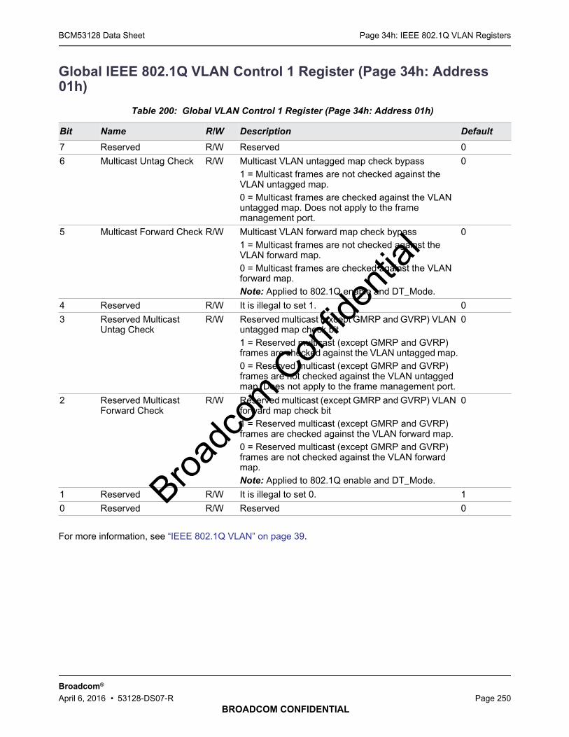
Page 34h: IEEE 802.1Q VLAN RegistersBCM53128 Data Sheet
BROADCOM CONFIDENTIAL
Broadcom®
April 6, 2016 • 53128-DS07-R Page 250
Global IEEE 802.1Q VLAN Control 1 Register (Page 34h: Address01h)
For more information, see “IEEE 802.1Q VLAN” on page 39.
Table 200: Global VLAN Control 1 Register (Page 34h: Address 01h)
Bit Name R/W Description Default
7 Reserved R/W Reserved 0
6 Multicast Untag Check R/W Multicast VLAN untagged map check bypass1 = Multicast frames are not checked against theVLAN untagged map.0 = Multicast frames are checked against the VLANuntagged map. Does not apply to the framemanagement port.
0
5 Multicast Forward Check R/W Multicast VLAN forward map check bypass1 = Multicast frames are not checked against theVLAN forward map.0 = Multicast frames are checked against the VLANforward map.Note: Applied to 802.1Q enable and DT_Mode.
0
4 Reserved R/W It is illegal to set 1. 0
3 Reserved MulticastUntag Check
R/W Reserved multicast (except GMRP and GVRP) VLANuntagged map check bit1 = Reserved multicast (except GMRP and GVRP)frames are checked against the VLAN untagged map.0 = Reserved multicast (except GMRP and GVRP)frames are not checked against the VLAN untaggedmap. Does not apply to the frame management port.
0
2 Reserved MulticastForward Check
R/W Reserved multicast (except GMRP and GVRP) VLANforward map check bit1 = Reserved multicast (except GMRP and GVRP)frames are checked against the VLAN forward map.0 = Reserved multicast (except GMRP and GVRP)frames are not checked against the VLAN forwardmap.Note: Applied to 802.1Q enable and DT_Mode.
0
1 Reserved R/W It is illegal to set 0. 1
0 Reserved R/W Reserved 0Broa
dcom
Con
fiden
tial
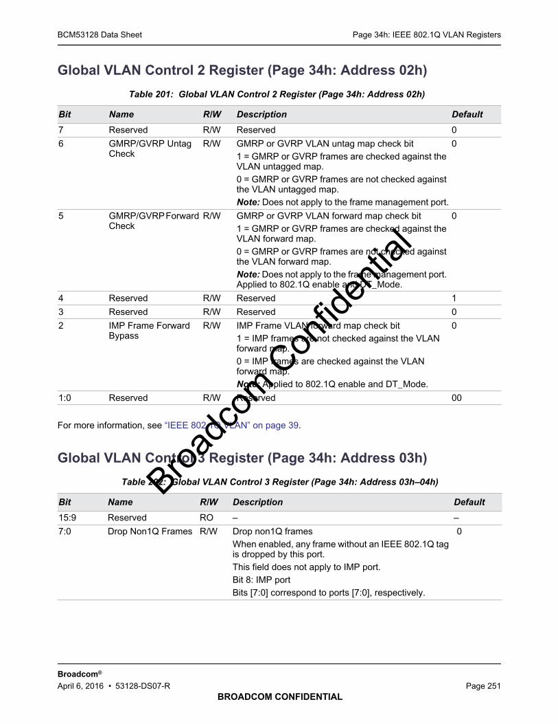
Page 34h: IEEE 802.1Q VLAN RegistersBCM53128 Data Sheet
BROADCOM CONFIDENTIAL
Broadcom®
April 6, 2016 • 53128-DS07-R Page 251
Global VLAN Control 2 Register (Page 34h: Address 02h)
For more information, see “IEEE 802.1Q VLAN” on page 39.
Global VLAN Control 3 Register (Page 34h: Address 03h)
Table 201: Global VLAN Control 2 Register (Page 34h: Address 02h)
Bit Name R/W Description Default
7 Reserved R/W Reserved 0
6 GMRP/GVRP UntagCheck
R/W GMRP or GVRP VLAN untag map check bit1 = GMRP or GVRP frames are checked against theVLAN untagged map.0 = GMRP or GVRP frames are not checked againstthe VLAN untagged map.Note: Does not apply to the frame management port.
0
5 GMRP/GVRPForwardCheck
R/W GMRP or GVRP VLAN forward map check bit1 = GMRP or GVRP frames are checked against theVLAN forward map.0 = GMRP or GVRP frames are not checked againstthe VLAN forward map.Note: Does not apply to the frame management port.Applied to 802.1Q enable and DT_Mode.
0
4 Reserved R/W Reserved 1
3 Reserved R/W Reserved 0
2 IMP Frame ForwardBypass
R/W IMP Frame VLAN forward map check bit1 = IMP frames are not checked against the VLANforward map.0 = IMP frames are checked against the VLANforward map.Note: Applied to 802.1Q enable and DT_Mode.
0
1:0 Reserved R/W Reserved 00
Table 202: Global VLAN Control 3 Register (Page 34h: Address 03h–04h)
Bit Name R/W Description Default
15:9 Reserved RO – –
7:0 Drop Non1Q Frames R/W Drop non1Q framesWhen enabled, any frame without an IEEE 802.1Q tagis dropped by this port.This field does not apply to IMP port.Bit 8: IMP portBits [7:0] correspond to ports [7:0], respectively.
0
Broadc
om C
onfid
entia
l
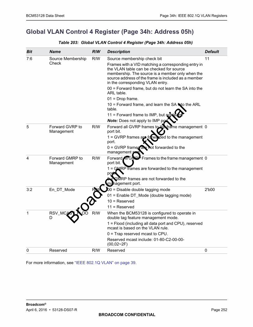
Page 34h: IEEE 802.1Q VLAN RegistersBCM53128 Data Sheet
BROADCOM CONFIDENTIAL
Broadcom®
April 6, 2016 • 53128-DS07-R Page 252
Global VLAN Control 4 Register (Page 34h: Address 05h)
For more information, see “IEEE 802.1Q VLAN” on page 39.
Table 203: Global VLAN Control 4 Register (Page 34h: Address 05h)
Bit Name R/W Description Default
7:6 Source MembershipCheck
R/W Source membership check bitFrames with a VID matching a corresponding entry inthe VLAN table can be checked for sourcemembership. The source is a member only when thesource address of the frame is included as a memberin the corresponding VLAN entry.00 = Forward frame, but do not learn the SA into theARL table.01 = Drop frame.10 = Forward frame, and learn the SA into the ARLtable.11 = Forward frame to IMP, but not learn.Note: Does not apply to IMP port.
11
5 Forward GVRP toManagement
R/W Forward all GVRP frames to the frame managementport bit.1 = GVRP frames are forwarded to the managementport.0 = GVRP frames are not forwarded to themanagement port.
0
4 Forward GMRP toManagement
R/W Forward All GMRP Frames to the frame managementport bit.1 = GMRP frames are forwarded to the managementport.0 = GMRP frames are not forwarded to themanagement port.
0
3:2 En_DT_Mode R/W 00 = Disable double tagging mode01 = Enable DT_Mode (double tagging mode)10 = Reserved11 = Reserved
2'b00
1 RSV_MCAST_FLOOD
R/W When the BCM53128 is configured to operate indouble tag feature management mode.1 = Flood (including all data port and CPU), reservedmcast is based on the VLAN rule.0 = Trap reserved mcast to CPU.Reserved mcast include: 01-80-C2-00-00-(00,02~2F)
0 Reserved R/W Reserved 0
Broadc
om C
onfid
entia
l

Page 34h: IEEE 802.1Q VLAN RegistersBCM53128 Data Sheet
BROADCOM CONFIDENTIAL
Broadcom®
April 6, 2016 • 53128-DS07-R Page 253
Global VLAN Control 5 Register (Page 34h: Address 06h)
For more information, see “IEEE 802.1Q VLAN” on page 39.
Table 204: Global VLAN Control 5 Register (Page 34h: Address 06h)
Bit Name R/W Description Default
7 Reserved R/W Reserved 0
6 Tag Status Preserve R/W IEEE 802.1Q tag/untag status preserved at egress.1 = Regardless of untag map in VLAN table, non-1Qframes (including 802.1p frames) will not be changedat TX (egress).This field has no effect in double tagging mode(DT_Mode).
0
5 Reserved R/W Reserved 0
4 Trunk Check Bypass R/W Trunk check bypass1 = Egress directed frames issued from the IMP portbypass trunk checking.0 = Egress directed frames issued from the IMP portare subject to trunk checking and redirection.
1
3 Drop Invalid VID R/W Drop frames with invalid VID.Frames with an invalid VID do not have acorresponding entry in the VLAN table.1 = Ingress frames with invalid VID are dropped.0 = Ingress frames with invalid VID are forwarded tothe IMP port.
0
2 VID_FFF_Fwding R/W Enable VID FFF forward1 = Forward frame0 = Comply with standard, drop frame
0
1 Reserved R/W Reserved 0
0 Management CRCCheck Bypass
R/W Bypass CRC check at the frame management port.1 = Ignore CRC check0 = Check CRC
0
Broadc
om C
onfid
entia
l
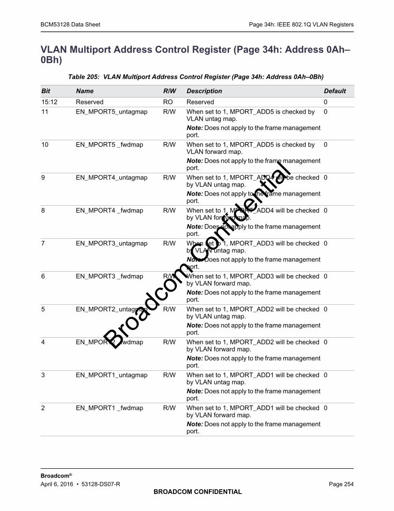
Page 34h: IEEE 802.1Q VLAN RegistersBCM53128 Data Sheet
BROADCOM CONFIDENTIAL
Broadcom®
April 6, 2016 • 53128-DS07-R Page 254
VLAN Multiport Address Control Register (Page 34h: Address 0Ah–0Bh)
Table 205: VLAN Multiport Address Control Register (Page 34h: Address 0Ah–0Bh)
Bit Name R/W Description Default
15:12 Reserved RO Reserved 0
11 EN_MPORT5_untagmap R/W When set to 1, MPORT_ADD5 is checked byVLAN untag map.Note: Does not apply to the frame managementport.
0
10 EN_MPORT5 _fwdmap R/W When set to 1, MPORT_ADD5 is checked byVLAN forward map.Note: Does not apply to the frame managementport.
0
9 EN_MPORT4_untagmap R/W When set to 1, MPORT_ADD4 will be checkedby VLAN untag map.Note: Does not apply to the frame managementport.
0
8 EN_MPORT4 _fwdmap R/W When set to 1, MPORT_ADD4 will be checkedby VLAN forward map.Note: Does not apply to the frame managementport.
0
7 EN_MPORT3_untagmap R/W When set to 1, MPORT_ADD3 will be checkedby VLAN untag map.Note: Does not apply to the frame managementport.
0
6 EN_MPORT3 _fwdmap R/W When set to 1, MPORT_ADD3 will be checkedby VLAN forward map.Note: Does not apply to the frame managementport.
0
5 EN_MPORT2_untagmap R/W When set to 1, MPORT_ADD2 will be checkedby VLAN untag map.Note: Does not apply to the frame managementport.
0
4 EN_MPORT2 _fwdmap R/W When set to 1, MPORT_ADD2 will be checkedby VLAN forward map.Note: Does not apply to the frame managementport.
0
3 EN_MPORT1_untagmap R/W When set to 1, MPORT_ADD1 will be checkedby VLAN untag map.Note: Does not apply to the frame managementport.
0
2 EN_MPORT1 _fwdmap R/W When set to 1, MPORT_ADD1 will be checkedby VLAN forward map.Note: Does not apply to the frame managementport.
0
Broadc
om C
onfid
entia
l
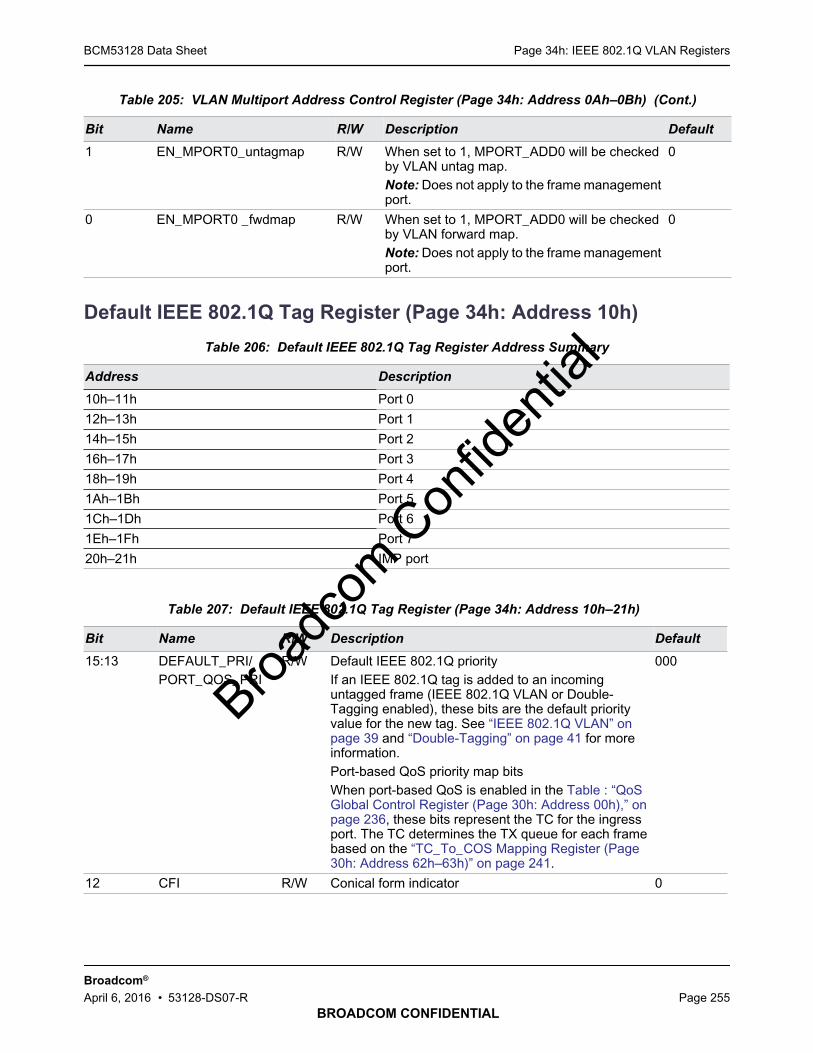
Page 34h: IEEE 802.1Q VLAN RegistersBCM53128 Data Sheet
BROADCOM CONFIDENTIAL
Broadcom®
April 6, 2016 • 53128-DS07-R Page 255
Default IEEE 802.1Q Tag Register (Page 34h: Address 10h)
1 EN_MPORT0_untagmap R/W When set to 1, MPORT_ADD0 will be checkedby VLAN untag map.Note: Does not apply to the frame managementport.
0
0 EN_MPORT0 _fwdmap R/W When set to 1, MPORT_ADD0 will be checkedby VLAN forward map.Note: Does not apply to the frame managementport.
0
Table 206: Default IEEE 802.1Q Tag Register Address Summary
Address Description
10h–11h Port 0
12h–13h Port 1
14h–15h Port 2
16h–17h Port 3
18h–19h Port 4
1Ah–1Bh Port 5
1Ch–1Dh Port 6
1Eh–1Fh Port 7
20h–21h IMP port
Table 207: Default IEEE 802.1Q Tag Register (Page 34h: Address 10h–21h)
Bit Name R/W Description Default
15:13 DEFAULT_PRI/PORT_QOS_PRI
R/W Default IEEE 802.1Q priorityIf an IEEE 802.1Q tag is added to an incominguntagged frame (IEEE 802.1Q VLAN or Double-Tagging enabled), these bits are the default priorityvalue for the new tag. See “IEEE 802.1Q VLAN” onpage 39 and “Double-Tagging” on page 41 for moreinformation.Port-based QoS priority map bitsWhen port-based QoS is enabled in the Table : “QoSGlobal Control Register (Page 30h: Address 00h),” onpage 236, these bits represent the TC for the ingressport. The TC determines the TX queue for each framebased on the “TC_To_COS Mapping Register (Page30h: Address 62h–63h)” on page 241.
000
12 CFI R/W Conical form indicator 0
Table 205: VLAN Multiport Address Control Register (Page 34h: Address 0Ah–0Bh) (Cont.)
Bit Name R/W Description Default
Broadc
om C
onfid
entia
l

Page 34h: IEEE 802.1Q VLAN RegistersBCM53128 Data Sheet
BROADCOM CONFIDENTIAL
Broadcom®
April 6, 2016 • 53128-DS07-R Page 256
Double Tagging TPID Register (Page 34h: Address 30h–31h)
ISP Port Selection Portmap Register (Page 34h: Address 32h–33h)
11:0 DEFAULT_VID R/W Default IEEE 802.1Q VLAN IDIf an IEEE 802.1Q tag is tagged to an incoming non-IEEE 802.1Q frame (IEEE 802.1Q VLAN or Double-Tagging enabled), then these bits are the default VIDfor the new tag. See “IEEE 802.1Q VLAN” on page 39and “Double-Tagging” on page 41 for more information.
001
Table 208: Double Tagging TPID Register (Page 34h: Address 30h–31h)
Bit Name R/W Description Default
15:0 ISP_TPID R/W The TPID used to identify double tagged frame. 9100
Table 209: ISP Port Selection Portmap Register (Page 34h: Address 32h–33h)
Bit Name R/W Description Default
15:9 RESERVED RO Reserved 0
8:0 ISP_Portmap R/W Bitmap that defines which port is designated as the ISPport.Bit 8: IMP portBits [7:0] correspond to ports [7:0], respectively.0 = Indicates that it is not an ISP port.1 = Indicates that it is an ISP port.
0
Table 207: Default IEEE 802.1Q Tag Register (Page 34h: Address 10h–21h) (Cont.)
Bit Name R/W Description Default
Broadc
om C
onfid
entia
l
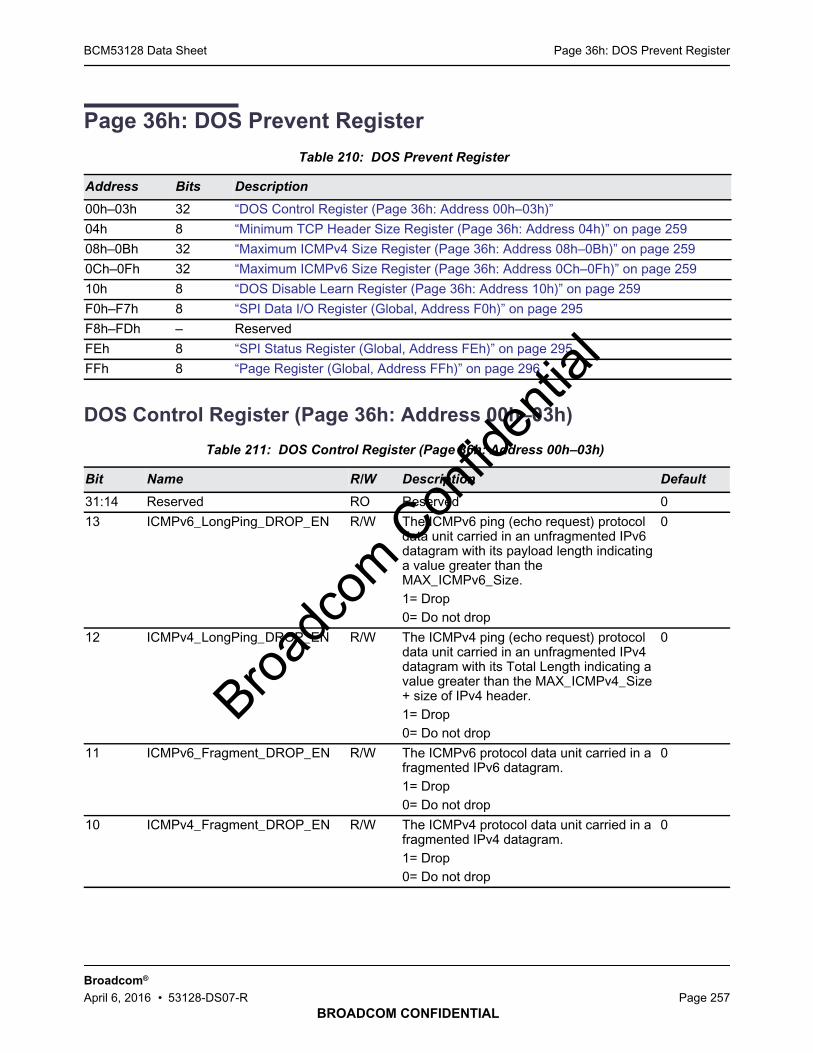
Page 36h: DOS Prevent RegisterBCM53128 Data Sheet
BROADCOM CONFIDENTIAL
Broadcom®
April 6, 2016 • 53128-DS07-R Page 257
Page 36h: DOS Prevent Register
DOS Control Register (Page 36h: Address 00h–03h)
Table 210: DOS Prevent Register
Address Bits Description
00h–03h 32 “DOS Control Register (Page 36h: Address 00h–03h)”
04h 8 “Minimum TCP Header Size Register (Page 36h: Address 04h)” on page 259
08h–0Bh 32 “Maximum ICMPv4 Size Register (Page 36h: Address 08h–0Bh)” on page 259
0Ch–0Fh 32 “Maximum ICMPv6 Size Register (Page 36h: Address 0Ch–0Fh)” on page 259
10h 8 “DOS Disable Learn Register (Page 36h: Address 10h)” on page 259
F0h–F7h 8 “SPI Data I/O Register (Global, Address F0h)” on page 295
F8h–FDh – Reserved
FEh 8 “SPI Status Register (Global, Address FEh)” on page 295
FFh 8 “Page Register (Global, Address FFh)” on page 296
Table 211: DOS Control Register (Page 36h: Address 00h–03h)
Bit Name R/W Description Default
31:14 Reserved RO Reserved 0
13 ICMPv6_LongPing_DROP_EN R/W The ICMPv6 ping (echo request) protocoldata unit carried in an unfragmented IPv6datagram with its payload length indicatinga value greater than theMAX_ICMPv6_Size.1= Drop0= Do not drop
0
12 ICMPv4_LongPing_DROP_EN R/W The ICMPv4 ping (echo request) protocoldata unit carried in an unfragmented IPv4datagram with its Total Length indicating avalue greater than the MAX_ICMPv4_Size+ size of IPv4 header.1= Drop0= Do not drop
0
11 ICMPv6_Fragment_DROP_EN R/W The ICMPv6 protocol data unit carried in afragmented IPv6 datagram.1= Drop0= Do not drop
0
10 ICMPv4_Fragment_DROP_EN R/W The ICMPv4 protocol data unit carried in afragmented IPv4 datagram.1= Drop0= Do not drop
0
Broadc
om C
onfid
entia
l
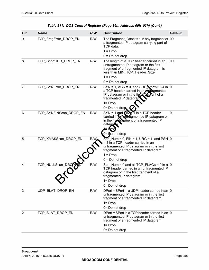
Page 36h: DOS Prevent RegisterBCM53128 Data Sheet
BROADCOM CONFIDENTIAL
Broadcom®
April 6, 2016 • 53128-DS07-R Page 258
9 TCP_FragError_DROP_EN R/W The Fragment_Offset = 1 in any fragment ofa fragmented IP datagram carrying part ofTCP data.1 = Drop0 = Do not drop
00
8 TCP_ShortHDR_DROP_EN R/W The length of a TCP header carried in anunfragmented IP datagram or the firstfragment of a fragmented IP datagram isless than MIN_TCP_Header_Size.1 = Drop0 = Do not drop
00
7 TCP_SYNError_DROP_EN R/W SYN = 1, ACK = 0, and SRC_Port<1024 ina TCP header carried in an unfragmentedIP datagram or in the first fragment of afragmented IP datagram.1= Drop0= Do not drop
0
6 TCP_SYNFINScan_DROP_EN R/W SYN = 1 and FIN = 1 in a TCP headercarried in an unfragmented IP datagram orin the first fragment of a fragmented IPdatagram.1= Drop0= Do not drop
0
5 TCP_XMASScan_DROP_EN R/W Seq_Num = 0, FIN = 1, URG = 1, and PSH= 1 in a TCP header carried in anunfragmented IP datagram or in the firstfragment of a fragmented IP datagram.1 = Drop0 = Do not drop
0
4 TCP_NULLScan_DROP_EN R/W Seq_Num = 0 and all TCP_FLAGs = 0 in aTCP header carried in an unfragmented IPdatagram or in the first fragment of afragmented IP datagram.1= Drop0= Do not drop
0
3 UDP_BLAT_DROP_EN R/W DPort = SPort in a UDP header carried in anunfragmented IP datagram or in the firstfragment of a fragmented IP datagram.1= Drop0= Do not drop
0
2 TCP_BLAT_DROP_EN R/W DPort = SPort in a TCP header carried in anunfragmented IP datagram or in the firstfragment of a fragmented IP datagram.1= Drop0= Do not drop
0
Table 211: DOS Control Register (Page 36h: Address 00h–03h) (Cont.)
Bit Name R/W Description Default
Broadc
om C
onfid
entia
l
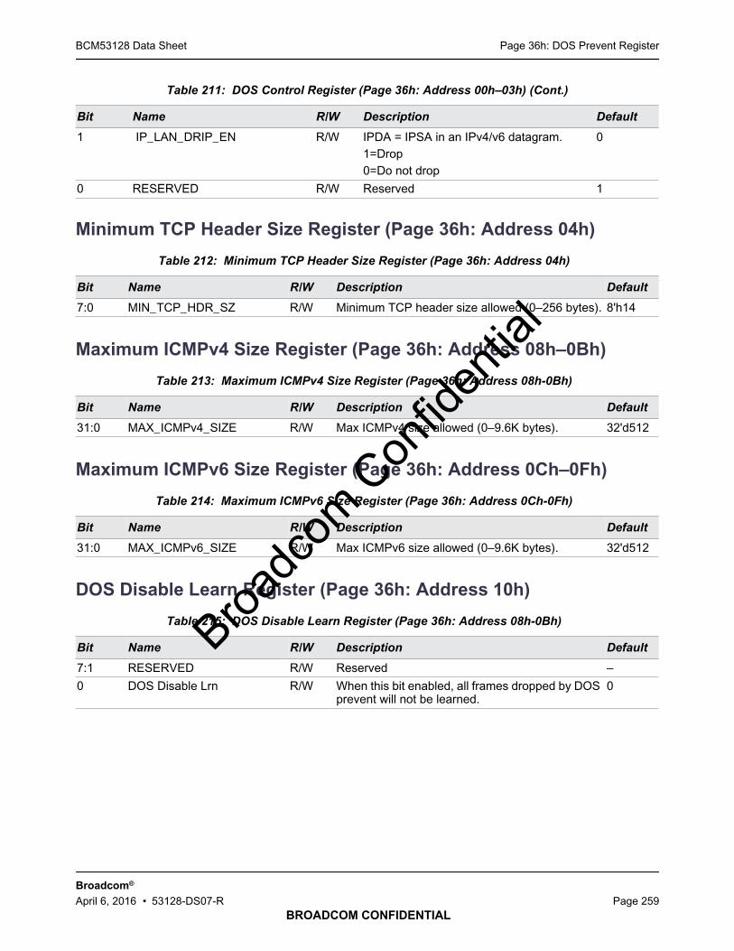
Page 36h: DOS Prevent RegisterBCM53128 Data Sheet
BROADCOM CONFIDENTIAL
Broadcom®
April 6, 2016 • 53128-DS07-R Page 259
Minimum TCP Header Size Register (Page 36h: Address 04h)
Maximum ICMPv4 Size Register (Page 36h: Address 08h–0Bh)
Maximum ICMPv6 Size Register (Page 36h: Address 0Ch–0Fh)
DOS Disable Learn Register (Page 36h: Address 10h)
1 IP_LAN_DRIP_EN R/W IPDA = IPSA in an IPv4/v6 datagram.1=Drop0=Do not drop
0
0 RESERVED R/W Reserved 1
Table 212: Minimum TCP Header Size Register (Page 36h: Address 04h)
Bit Name R/W Description Default
7:0 MIN_TCP_HDR_SZ R/W Minimum TCP header size allowed (0–256 bytes). 8'h14
Table 213: Maximum ICMPv4 Size Register (Page 36h: Address 08h-0Bh)
Bit Name R/W Description Default
31:0 MAX_ICMPv4_SIZE R/W Max ICMPv4 size allowed (0–9.6K bytes). 32'd512
Table 214: Maximum ICMPv6 Size Register (Page 36h: Address 0Ch-0Fh)
Bit Name R/W Description Default
31:0 MAX_ICMPv6_SIZE R/W Max ICMPv6 size allowed (0–9.6K bytes). 32'd512
Table 215: DOS Disable Learn Register (Page 36h: Address 08h-0Bh)
Bit Name R/W Description Default
7:1 RESERVED R/W Reserved –
0 DOS Disable Lrn R/W When this bit enabled, all frames dropped by DOSprevent will not be learned.
0
Table 211: DOS Control Register (Page 36h: Address 00h–03h) (Cont.)
Bit Name R/W Description Default
Broadc
om C
onfid
entia
l

Page 40h: Jumbo Frame Control RegisterBCM53128 Data Sheet
BROADCOM CONFIDENTIAL
Broadcom®
April 6, 2016 • 53128-DS07-R Page 260
Page 40h: Jumbo Frame Control Register
Jumbo Frame Port Mask Register (Page 40h: Address 01h)
Table 216: Page 40h Jumbo Frame Control Register
Address Bits Description
00h – Reserved
01h–04h 32 “Jumbo Frame Port Mask Register (Page 40h: Address 01h)”
05h–06h 16 “Standard Max Frame Size Register (Page 40h: Address 05h)” onpage 261
07h–EFh – Reserved
F0h–F7h 8 “SPI Data I/O Register (Global, Address F0h)” on page 295, bytes 0–7
F8h–FDh – Reserved
FEh 8 “SPI Status Register (Global, Address FEh)” on page 295
FFh 8 “Page Register (Global, Address FFh)” on page 296
Table 217: Jumbo Frame Port Mask Registers (Page 40h: Address 01h–04h)
BIt Name R/W Description Default
31:25 Reserved RO Reserved 0
24:9 Reserved R/W Reserved 0
8:0 JUMBO_PORT_MASK R/W Jumbo frame port maskBit 8: IMP portBits [7:0] correspond to ports [7:0], respectively.0 = Disable jumbo frame capability on the port.1 = Enable jumbo frame capability on the port.Jumbo frames can be ingressed and egressed only to theports enabled via this port mask. Jumbo frame port maskhas no effect on the traffic of normal sized frames. See“Jumbo Frame Support” on page 44 for more information.
0
Note: When the Jumbo Frame feature is enabled, the assigned Weight value for the WRR schedulingcannot be applied fairly over the queues. This is due to the internal Packet Buffer Memory sizelimitation.
Note: The Jumbo Frame feature is only supported in 1000 Mbps mode.
Broadc
om C
onfid
entia
l
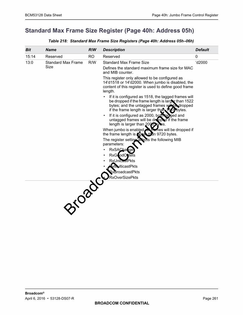
Page 40h: Jumbo Frame Control RegisterBCM53128 Data Sheet
BROADCOM CONFIDENTIAL
Broadcom®
April 6, 2016 • 53128-DS07-R Page 261
Standard Max Frame Size Register (Page 40h: Address 05h)
Table 218: Standard Max Frame Size Registers (Page 40h: Address 05h–06h)
Bit Name R/W Description Default
15:14 Reserved RO Reserved 0
13:0 Standard Max FrameSize
R/W Standard Max Frame SizeDefines the standard maximum frame size for MACand MIB counter.This register only allowed to be configured as14'd1518 or 14'd2000. When jumbo is disabled, thecontent of this register is used to define good framelength.• If it is configured as 1518, the tagged frames will
be dropped if the frame length is larger than 1522bytes; and the untagged frames will be droppedif the frame length is larger than 1518 bytes.
• If it is configured as 2000, both tagged anduntagged frames will be dropped if the framelength is larger than 2000 bytes.
When jumbo is enabled, all frames will be dropped ifthe frame length is larger than 9720 bytes.The register setting affects the following MIBparameters:• RxSAChange• RxGoodOctets• RxUnicastPkts• RxMulticastPkts• RxBroadcastPkts• RxOverSizePkts
‘d2000
Broadc
om C
onfid
entia
l
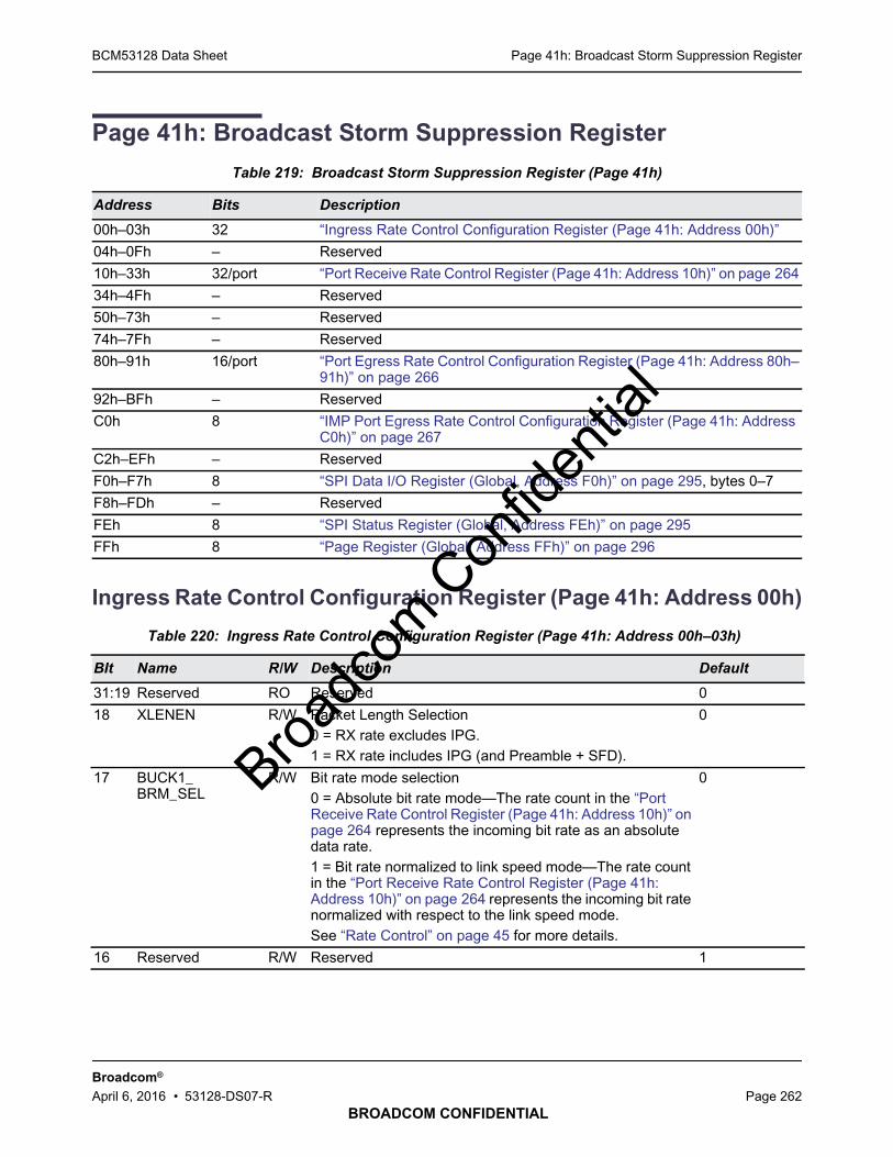
Page 41h: Broadcast Storm Suppression RegisterBCM53128 Data Sheet
BROADCOM CONFIDENTIAL
Broadcom®
April 6, 2016 • 53128-DS07-R Page 262
Page 41h: Broadcast Storm Suppression Register
Ingress Rate Control Configuration Register (Page 41h: Address 00h)
Table 219: Broadcast Storm Suppression Register (Page 41h)
Address Bits Description
00h–03h 32 “Ingress Rate Control Configuration Register (Page 41h: Address 00h)”
04h–0Fh – Reserved
10h–33h 32/port “Port Receive Rate Control Register (Page 41h: Address 10h)” on page 264
34h–4Fh – Reserved
50h–73h – Reserved
74h–7Fh – Reserved
80h–91h 16/port “Port Egress Rate Control Configuration Register (Page 41h: Address 80h–91h)” on page 266
92h–BFh – Reserved
C0h 8 “IMP Port Egress Rate Control Configuration Register (Page 41h: AddressC0h)” on page 267
C2h–EFh – Reserved
F0h–F7h 8 “SPI Data I/O Register (Global, Address F0h)” on page 295, bytes 0–7
F8h–FDh – Reserved
FEh 8 “SPI Status Register (Global, Address FEh)” on page 295
FFh 8 “Page Register (Global, Address FFh)” on page 296
Table 220: Ingress Rate Control Configuration Register (Page 41h: Address 00h–03h)
BIt Name R/W Description Default
31:19 Reserved RO Reserved 0
18 XLENEN R/W Packet Length Selection0 = RX rate excludes IPG.1 = RX rate includes IPG (and Preamble + SFD).
0
17 BUCK1_BRM_SEL
R/W Bit rate mode selection0 = Absolute bit rate mode—The rate count in the “PortReceive Rate Control Register (Page 41h: Address 10h)” onpage 264 represents the incoming bit rate as an absolutedata rate.1 = Bit rate normalized to link speed mode—The rate countin the “Port Receive Rate Control Register (Page 41h:Address 10h)” on page 264 represents the incoming bit ratenormalized with respect to the link speed mode.See “Rate Control” on page 45 for more details.
0
16 Reserved R/W Reserved 1
Broadc
om C
onfid
entia
l
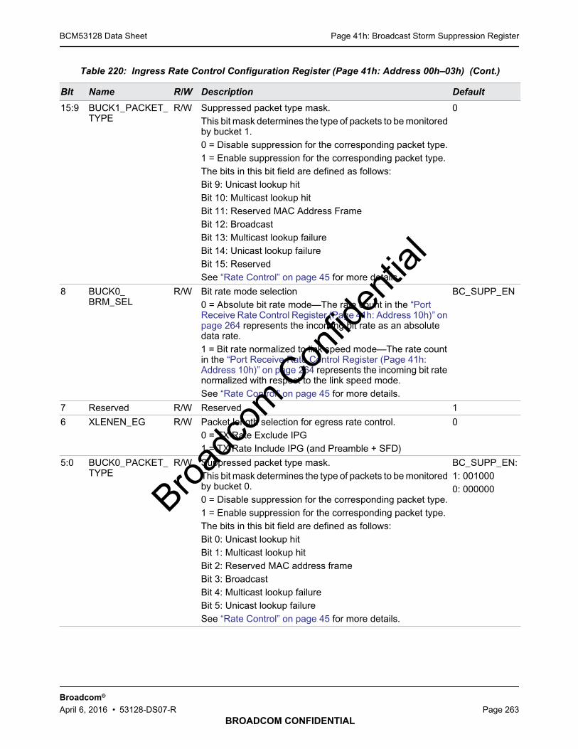
Page 41h: Broadcast Storm Suppression RegisterBCM53128 Data Sheet
BROADCOM CONFIDENTIAL
Broadcom®
April 6, 2016 • 53128-DS07-R Page 263
15:9 BUCK1_PACKET_TYPE
R/W Suppressed packet type mask.This bit mask determines the type of packets to be monitoredby bucket 1.0 = Disable suppression for the corresponding packet type.1 = Enable suppression for the corresponding packet type.The bits in this bit field are defined as follows:Bit 9: Unicast lookup hitBit 10: Multicast lookup hitBit 11: Reserved MAC Address FrameBit 12: BroadcastBit 13: Multicast lookup failureBit 14: Unicast lookup failureBit 15: ReservedSee “Rate Control” on page 45 for more details.
0
8 BUCK0_BRM_SEL
R/W Bit rate mode selection0 = Absolute bit rate mode—The rate count in the “PortReceive Rate Control Register (Page 41h: Address 10h)” onpage 264 represents the incoming bit rate as an absolutedata rate.1 = Bit rate normalized to link speed mode—The rate countin the “Port Receive Rate Control Register (Page 41h:Address 10h)” on page 264 represents the incoming bit ratenormalized with respect to the link speed mode.See “Rate Control” on page 45 for more details.
BC_SUPP_EN
7 Reserved R/W Reserved 1
6 XLENEN_EG R/W Packet length selection for egress rate control.0 = TX Rate Exclude IPG1 = TX Rate Include IPG (and Preamble + SFD)
0
5:0 BUCK0_PACKET_TYPE
R/W Suppressed packet type mask.This bit mask determines the type of packets to be monitoredby bucket 0.0 = Disable suppression for the corresponding packet type.1 = Enable suppression for the corresponding packet type.The bits in this bit field are defined as follows:Bit 0: Unicast lookup hitBit 1: Multicast lookup hitBit 2: Reserved MAC address frameBit 3: BroadcastBit 4: Multicast lookup failureBit 5: Unicast lookup failureSee “Rate Control” on page 45 for more details.
BC_SUPP_EN:1: 0010000: 000000
Table 220: Ingress Rate Control Configuration Register (Page 41h: Address 00h–03h) (Cont.)
BIt Name R/W Description Default
Broadc
om C
onfid
entia
l

Page 41h: Broadcast Storm Suppression RegisterBCM53128 Data Sheet
BROADCOM CONFIDENTIAL
Broadcom®
April 6, 2016 • 53128-DS07-R Page 264
Port Receive Rate Control Register (Page 41h: Address 10h)
Table 221: Port Rate Control Register Address Summary
Address Description
10h–13h Port 0
14h–17h Port 1
18h–1Bh Port 2
1Ch–1Fh Port 3
20h–23h Port 4
24h–27h Port 5
28h–2Bh Port 6
2Ch–2Fh Port 7
30h–33h IMP port for BCM53128
Table 222: Port Rate Control Register (Page 41h: Address 10h–33h)
BIt Name R/W Description Default
31:29 Reserved RO Reserved 0
28 STRM_SUPR_EN R/W Enable storm suppression (Supported by bucket1).0 = Disable1 = Enable
Reflects thestrap pinBC_SUPP_EN
27 RsvMC_SUPR_EN R/W Enable reserved mulitcast storm suppression.0 = Disable1 = Enable
0
26 BC_SUPR_EN R/W Enable broadcast storm suppression.0 = Disable1 = Enable
0
25 MC_SUPR_EN R/W Enable multicast storm suppression.0 = Disable1 = Enable
0
24 DLF_SUPR_EN R/W Enable DLF storm suppression.0 = Disable1 = Enable
0
23 Enable Bucket1 R/W Enable rate control of the ingress port, bucket 1.0 = Disable1 = Enable
0
22 Enable Bucket0 R/W Enable rate control of the ingress port, bucket 0.0 = Disable1 = Enable
Reflects thestrap pinBC_SUPP_EN
Broadc
om C
onfid
entia
l

Page 41h: Broadcast Storm Suppression RegisterBCM53128 Data Sheet
BROADCOM CONFIDENTIAL
Broadcom®
April 6, 2016 • 53128-DS07-R Page 265
21:19 BUCK1_SIZE R/W Bucket sizeThis bit determines the maximum size of bucket 1. This isspecified on a per port basis.000 = 4 KB001 = 8 KB010 = 16 KB011 = 32 KB100 = 64 KB101 = 500 KB110 = 500 KB111 = 500 KBSee “Rate Control” on page 45 for more details.
000
18:11 BUCK1_Rate_Cnt R/W Rate countThe rate count is an integer that increments the rate atwhich traffic can ingress the given port without beingsuppressed. This value is specified on a per port basis.The programmed values of the rate count and the bit ratemode of the “Ingress Rate Control Configuration Register(Page 41h: Address 00h)” on page 262 determine thebucket bit rate in kilobytes. The bucket bit rate representsthe average upper limit for incoming packets selected inthe suppressed packet type mask in the “Ingress RateControl Configuration Register (Page 41h: Address 00h)”on page 262. See “Rate Control” on page 45 for moredetails.Values written to these bits must be with the rangesspecified by Table 3 on page 47. Values outside theseranges are not valid.
10h
10:8 BUCK0_SIZE R/W Bucket sizeThis bit determines the maximum size of bucket 0. This isspecified on a per port basis.000 = 4 KB001 = 8 KB010 = 16 KB011 = 32 KB100 = 64 KB101 = 500 KB110 = 500 KB111 = 500 KBSee “Rate Control” on page 45 for more details.
000
Table 222: Port Rate Control Register (Page 41h: Address 10h–33h) (Cont.)
BIt Name R/W Description Default
Broadc
om C
onfid
entia
l

Page 41h: Broadcast Storm Suppression RegisterBCM53128 Data Sheet
BROADCOM CONFIDENTIAL
Broadcom®
April 6, 2016 • 53128-DS07-R Page 266
Port Egress Rate Control Configuration Register (Page 41h: Address80h–91h)
7:0 BUCK0_Rate_Cnt R/W Rate countThe rate count is an integer that increments the rate atwhich traffic can ingress the given port without beingsuppressed. This value is specified on a per port basis.The programmed values of the rate count and the bit ratemode of the “Ingress Rate Control Configuration Register(Page 41h: Address 00h)” on page 262 determine thebucket bit rate in kilobytes. The bucket bit rate representsthe average upper limit for incoming packets selected inthe Suppressed packet type mask in the “Ingress RateControl Configuration Register (Page 41h: Address 00h)”on page 262. See “Rate Control” on page 45 for moredetails.
10h
Table 223: Port Egress Rate Control Configuration Register Address Summary
Address Description
80h–81h Port 0
82h–83h Port 1
84h–85h Port 2
86h–87h Port 3
88h–89h Port 4
8Ah–8Bh Port 5
8Ch–8Dh Port 6
8Eh–8Fh Port 7
90h–91h IMP port
Table 224: Port Egress Rate Control Configuration Registers (Page 41h: Address 80h–91h)
BIt Name R/W DescriptionDefault
15:12 Reserved RO Reserved 0
11 ERC_EN R/W Egress rate control enable ((Absolute Bit Rate) 0
Table 222: Port Rate Control Register (Page 41h: Address 10h–33h) (Cont.)
BIt Name R/W Description Default
Broadc
om C
onfid
entia
l

Page 41h: Broadcast Storm Suppression RegisterBCM53128 Data Sheet
BROADCOM CONFIDENTIAL
Broadcom®
April 6, 2016 • 53128-DS07-R Page 267
IMP Port Egress Rate Control Configuration Register (Page 41h:Address C0h)
10:8 BKT_SZE R/W Bucket sizeThis bit determines the maximum size of bucket 0. This isspecified on a per port basis.000 = 4 KB001 = 8 KB010 = 16 KB011 = 32 KB100 = 64 KB101 = 500 KB110 = 500 KB111 = 500 KBSee “Rate Control” on page 45 for more details.
0
7:0 RATE_CNT R/W Rate count for bucket 0
Table 225: IMP Port Egress Rate Control Configuration Register Address Summary
Address Description
C0h IMP Port
Table 226: IMP Port Egress Rate Control Configuration Registers (Page 41h: Address C0h)
BIt Name R/W DescriptionDefault
7:6 RESERVED RO Reserved 0
5:0 Rate_Index R/W Rate_Index is used to configure different egress rates for IMP inpacket per second (pps). See Table 227: “Using Rate_Index toConfigure Different Egress Rates for IMP in pps,” on page 268.When set to 0, the egress rate is limited to a maximum of 384 pps.When set to 63, the egress rate control function is disabled and allpackets are transmitted at wire-speed.Note: If the Rate_Index is configured as a certain value, theegress rate is limited to the corresponding speed whether theswitch is running at 10 Mbps, 100 Mbps, or 1 Gbps.Note: The Rate_Index should be a reasonable value under thecorresponding network speed configuration. It does not makesense to set a value of 63 with the network configuration at 10Mbps. In that case, the egress rate is limited up to 10 Mbps.
6'd63
Table 224: Port Egress Rate Control Configuration Registers (Page 41h: Address 80h–91h) (Cont.)
BIt Name R/W DescriptionDefault
Broadc
om C
onfid
entia
l

Page 42h: EAP RegisterBCM53128 Data Sheet
BROADCOM CONFIDENTIAL
Broadcom®
April 6, 2016 • 53128-DS07-R Page 268
Page 42h: EAP Register
Table 227: Using Rate_Index to Configure Different Egress Rates for IMP in pps
Rate_Index pps Rate_Index pps Rate_Index pps Rate_Index pps
0 384 16 5376 32 25354 48 357143
1 512 17 5887 33 27382 49 423729
2 639 18 6400 34 29446 50 500000
3 768 19 6911 35 31486 51 568182
4 1024 20 7936 36 35561 52 641026
5 1280 21 8960 37 39682 53 714286
6 1536 22 9984 38 42589 54 781250
7 1791 23 11008 39 56818 55 862069
8 2048 24 12030 40 71023 56 925926
9 2303 25 13054 41 85324 57 1000000
10 2559 26 14076 42 99602 58 1086957
11 2815 27 15105 43 113636 59 1136364
12 3328 28 17146 44 127551 60 1190476
13 3840 29 19201 45 142045 61 1250000
14 4352 30 21240 46 213675 62 1315789
15 4863 31 23299 47 284091 63 1388889
Table 228: Broadcast Storm Suppression Register (Page 42h)
Address Bits Description
00h 8 “EAP Global Control Register (Page 42h: Address 00h)” on page 269
01h 8 “EAP Multiport Address Control Register (Page 42h: Address 01h)” on page 269
02h–09h 64 “EAP Destination IP Register 0 (Page 42h: Address 02h)” on page 270
0Ah–12h 64 “EAP Destination IP Register 1 (Page 42h: Address 0Ah)” on page 270
20h–5Fh 64 “Port EAP Configuration Register (Page 42h: Address 20h)” on page 271
60h–EFh – Reserved
F0h–F7h 8 “SPI Data I/O Register (Global, Address F0h)” on page 295, bytes 0–7
F8h–FDh – Reserved
FEh 8 “SPI Status Register (Global, Address FEh)” on page 295
FFh 8 “Page Register (Global, Address FFh)” on page 296
Broadc
om C
onfid
entia
l
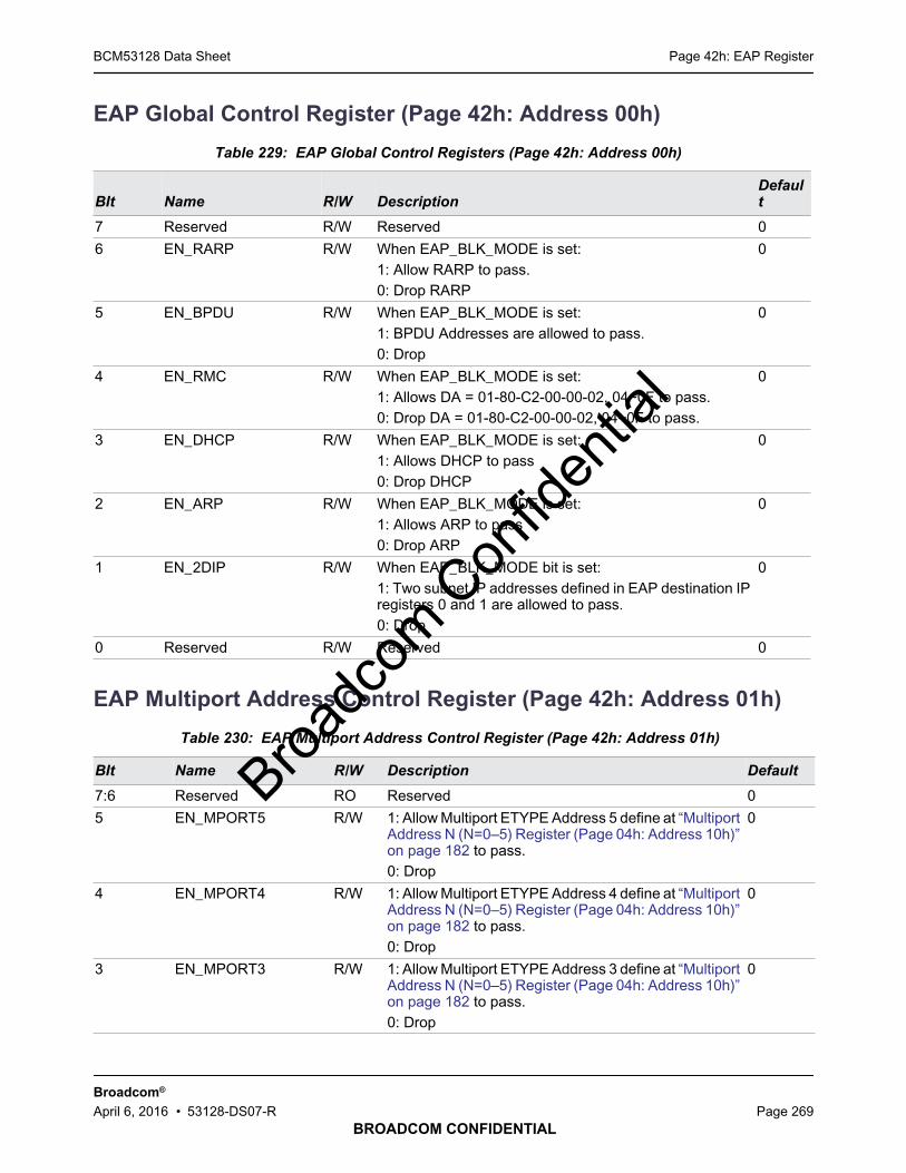
Page 42h: EAP RegisterBCM53128 Data Sheet
BROADCOM CONFIDENTIAL
Broadcom®
April 6, 2016 • 53128-DS07-R Page 269
EAP Global Control Register (Page 42h: Address 00h)
EAP Multiport Address Control Register (Page 42h: Address 01h)
Table 229: EAP Global Control Registers (Page 42h: Address 00h)
BIt Name R/W DescriptionDefault
7 Reserved R/W Reserved 0
6 EN_RARP R/W When EAP_BLK_MODE is set:1: Allow RARP to pass.0: Drop RARP
0
5 EN_BPDU R/W When EAP_BLK_MODE is set:1: BPDU Addresses are allowed to pass.0: Drop
0
4 EN_RMC R/W When EAP_BLK_MODE is set:1: Allows DA = 01-80-C2-00-00-02, 04~0F to pass.0: Drop DA = 01-80-C2-00-00-02, 04~0F to pass.
0
3 EN_DHCP R/W When EAP_BLK_MODE is set:1: Allows DHCP to pass0: Drop DHCP
0
2 EN_ARP R/W When EAP_BLK_MODE is set:1: Allows ARP to pass0: Drop ARP
0
1 EN_2DIP R/W When EAP_BLK_MODE bit is set:1: Two subnet IP addresses defined in EAP destination IPregisters 0 and 1 are allowed to pass.0: Drop
0
0 Reserved R/W Reserved 0
Table 230: EAP Multiport Address Control Register (Page 42h: Address 01h)
BIt Name R/W Description Default
7:6 Reserved RO Reserved 0
5 EN_MPORT5 R/W 1: Allow Multiport ETYPE Address 5 define at “MultiportAddress N (N=0–5) Register (Page 04h: Address 10h)”on page 182 to pass.0: Drop
0
4 EN_MPORT4 R/W 1: Allow Multiport ETYPE Address 4 define at “MultiportAddress N (N=0–5) Register (Page 04h: Address 10h)”on page 182 to pass.0: Drop
0
3 EN_MPORT3 R/W 1: Allow Multiport ETYPE Address 3 define at “MultiportAddress N (N=0–5) Register (Page 04h: Address 10h)”on page 182 to pass.0: Drop
0
Broadc
om C
onfid
entia
l

Page 42h: EAP RegisterBCM53128 Data Sheet
BROADCOM CONFIDENTIAL
Broadcom®
April 6, 2016 • 53128-DS07-R Page 270
EAP Destination IP Register 0 (Page 42h: Address 02h)
EAP Destination IP Register 1 (Page 42h: Address 0Ah)
2 EN_MPORT2 R/W 1: Allow Multiport ETYPE Address 2 define at “MultiportAddress N (N=0–5) Register (Page 04h: Address 10h)”on page 182 to pass.0: Drop
0
1 EN_MPORT1 R/W 1: Allow Multiport ETYPE Address 1 define at “MultiportAddress N (N=0–5) Register (Page 04h: Address 10h)”on page 182 to pass.0: Drop
0
0 EN_MPORT0 R/W 1: Allow Multiport ETYPE Address 0 define at “MultiportAddress N (N=0–5) Register (Page 04h: Address 10h)”on page 182 to pass.0: Drop
0
Table 231: EAP Destination IP Registers 0 (Page 42h: Address 02h–09h)
BIt Name R/W Description Default
63:32 DIP_SUB 0 R/W EAP destination IP subnet register 0 0
31: 0 DIP_MSK 0 R/W EAP destination IP mask register 0 0
Table 232: EAP Destination IP Registers 1 (Page 42h: Address 0Ah–12h)
BIt Name R/W Description Default
63:32 DIP_SUB 1 R/W EAP destination IP subnet register 1 0
31:0 DIP_MSK 1 R/W EAP destination IP mask register 1 0
Table 230: EAP Multiport Address Control Register (Page 42h: Address 01h) (Cont.)
BIt Name R/W Description Default
Broadc
om C
onfid
entia
l

Page 42h: EAP RegisterBCM53128 Data Sheet
BROADCOM CONFIDENTIAL
Broadcom®
April 6, 2016 • 53128-DS07-R Page 271
Port EAP Configuration Register (Page 42h: Address 20h)
Table 233: Port EAP Configuration Register Address Summary
Address Description
20h–27h Port 0
28h–2Fh Port 1
30h–37h Port 2
38h–3Fh Port 3
40h–47h Port 4
48h–4Fh Port 5
50h–57h Port 6
58h–5Fh Port 7
Table 234: Port EAP Configuration Registers (Page 42h: Address 20h–47h)
BIt Name R/W Description Default
63:55 Reserved RO Reserved 0
52:51 EAP_MODE R/W 00 = Basic mode, do not check SA.01 = Reserved10 = Extend mode, check SA and port number, drop if SAis unknown.11 = Simplified mode, check SA and port number trap tomanagement port if SA is unknown.
0
50:49 EAP_BLK_MODE R/W 00: Do not check EAP_BLK_MODE.01: To check EAP_BLK MODE on ingress port, only theframe defined in EAP_GCFG will be forwarded.Otherwise, the frame will be dropped.10: reserved11: To check EAP_BLK MODE on both ingress and egressport, only the frame defined in EAP_GCFG will beforwarded. The forwarding process will verify that eachegress port is at block mode.
0
48 EAP_EN_DA R/W Enable EAP frame with DA 0
47:0 EAP_DA R/W EAP frame DA register 00-00-00-00-00-00
Broadc
om C
onfid
entia
l
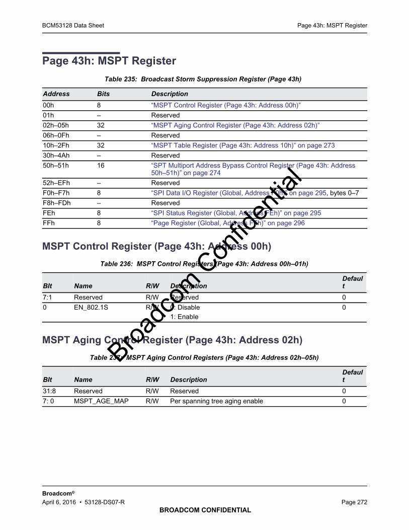
Page 43h: MSPT RegisterBCM53128 Data Sheet
BROADCOM CONFIDENTIAL
Broadcom®
April 6, 2016 • 53128-DS07-R Page 272
Page 43h: MSPT Register
MSPT Control Register (Page 43h: Address 00h)
MSPT Aging Control Register (Page 43h: Address 02h)
Table 235: Broadcast Storm Suppression Register (Page 43h)
Address Bits Description
00h 8 “MSPT Control Register (Page 43h: Address 00h)”
01h – Reserved
02h–05h 32 “MSPT Aging Control Register (Page 43h: Address 02h)”
06h–0Fh – Reserved
10h–2Fh 32 “MSPT Table Register (Page 43h: Address 10h)” on page 273
30h–4Ah – Reserved
50h–51h 16 “SPT Multiport Address Bypass Control Register (Page 43h: Address50h–51h)” on page 274
52h–EFh – Reserved
F0h–F7h 8 “SPI Data I/O Register (Global, Address F0h)” on page 295, bytes 0–7
F8h–FDh – Reserved
FEh 8 “SPI Status Register (Global, Address FEh)” on page 295
FFh 8 “Page Register (Global, Address FFh)” on page 296
Table 236: MSPT Control Registers (Page 43h: Address 00h–01h)
BIt Name R/W DescriptionDefault
7:1 Reserved R/W Reserved 0
0 EN_802.1S R/W 0: Disable1: Enable
0
Table 237: MSPT Aging Control Registers (Page 43h: Address 02h–05h)
BIt Name R/W DescriptionDefault
31:8 Reserved R/W Reserved 0
7: 0 MSPT_AGE_MAP R/W Per spanning tree aging enable 0
Broadc
om C
onfid
entia
l

Page 43h: MSPT RegisterBCM53128 Data Sheet
BROADCOM CONFIDENTIAL
Broadcom®
April 6, 2016 • 53128-DS07-R Page 273
MSPT Table Register (Page 43h: Address 10h)
Table 238: MSPT Table Register Address Summary
Address Description
10h–13h MSPT 0
14h–17h MSPT 1
18h–1Bh MSPT 2
1Ch–1Fh MSPT 3
20h–23h MSPT 4
24h–27h MSPT 5
28h–2Bh MSPT 6
2Ch–2Fh MSPT 7
Table 239: MSPT Table Registers (Page 43h: Address 10h–2Fh)
BIt Name R/W DescriptionDefault
31:27 Reserved RO Reserved 0
26:24 Reserved R/W Reserved 0
23:21 Reserved R/W Spanning tree state for port 7 0
20:18 Reserved R/W Spanning tree state for port 6 0
17:15 SPT_STA5 R/W Spanning tree state for port 5 0
14:12 SPT_STA4 R/W Spanning tree state for port 4000 = No spanning tree001 = Disabled010 = Blocking011 = Listening100 = Learning101 = Forwarding
0
11:9 SPT_STA3 R/W Spanning tree state for port 3 0
8:6 SPT_STA2 R/W Spanning tree state for port 2 0
5:3 SPT_STA1 R/W Spanning tree state for port 1 0
2:0 SPT_STA0 R/W Spanning tree state for port 0 0Broa
dcom
Con
fiden
tial
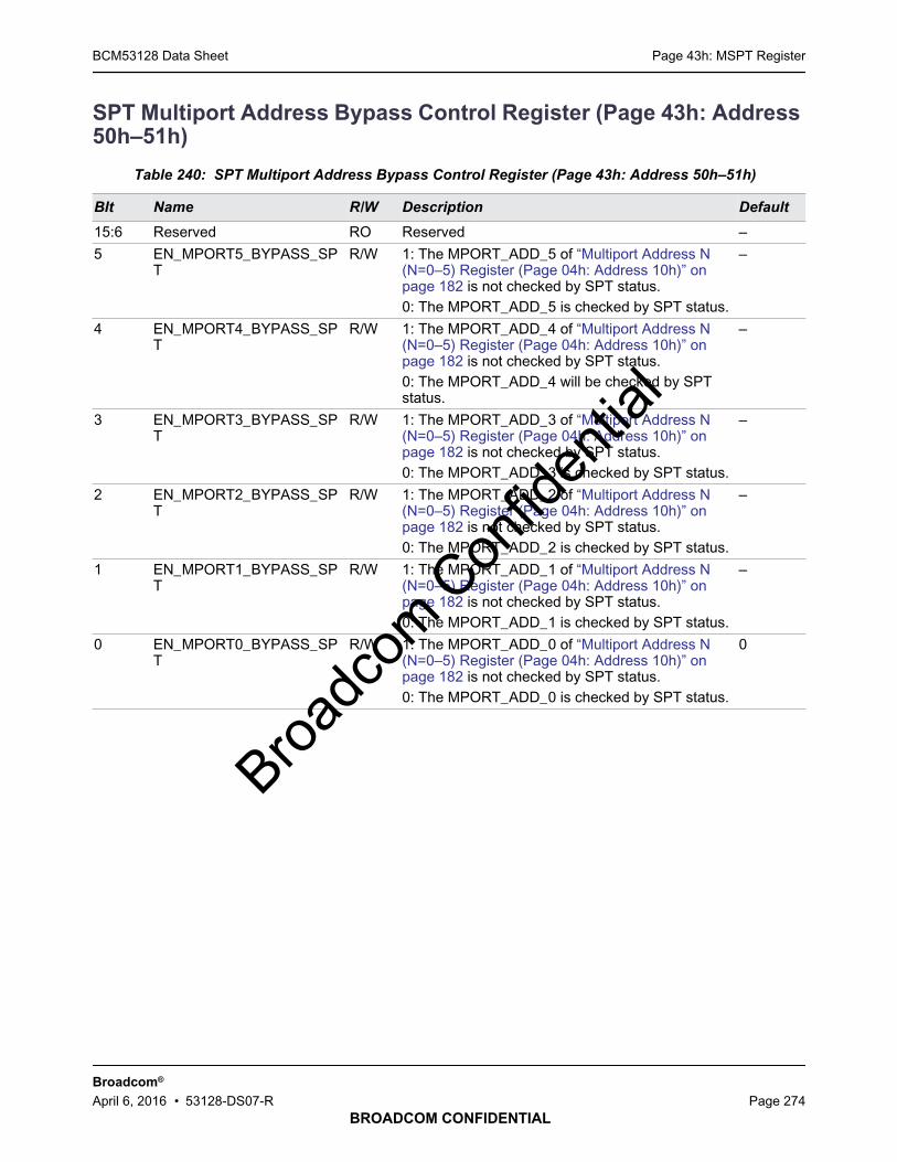
Page 43h: MSPT RegisterBCM53128 Data Sheet
BROADCOM CONFIDENTIAL
Broadcom®
April 6, 2016 • 53128-DS07-R Page 274
SPT Multiport Address Bypass Control Register (Page 43h: Address50h–51h)
Table 240: SPT Multiport Address Bypass Control Register (Page 43h: Address 50h–51h)
BIt Name R/W Description Default
15:6 Reserved RO Reserved –
5 EN_MPORT5_BYPASS_SPT
R/W 1: The MPORT_ADD_5 of “Multiport Address N(N=0–5) Register (Page 04h: Address 10h)” onpage 182 is not checked by SPT status.0: The MPORT_ADD_5 is checked by SPT status.
–
4 EN_MPORT4_BYPASS_SPT
R/W 1: The MPORT_ADD_4 of “Multiport Address N(N=0–5) Register (Page 04h: Address 10h)” onpage 182 is not checked by SPT status.0: The MPORT_ADD_4 will be checked by SPTstatus.
–
3 EN_MPORT3_BYPASS_SPT
R/W 1: The MPORT_ADD_3 of “Multiport Address N(N=0–5) Register (Page 04h: Address 10h)” onpage 182 is not checked by SPT status.0: The MPORT_ADD_3 is checked by SPT status.
–
2 EN_MPORT2_BYPASS_SPT
R/W 1: The MPORT_ADD_2 of “Multiport Address N(N=0–5) Register (Page 04h: Address 10h)” onpage 182 is not checked by SPT status.0: The MPORT_ADD_2 is checked by SPT status.
–
1 EN_MPORT1_BYPASS_SPT
R/W 1: The MPORT_ADD_1 of “Multiport Address N(N=0–5) Register (Page 04h: Address 10h)” onpage 182 is not checked by SPT status.0: The MPORT_ADD_1 is checked by SPT status.
–
0 EN_MPORT0_BYPASS_SPT
R/W 1: The MPORT_ADD_0 of “Multiport Address N(N=0–5) Register (Page 04h: Address 10h)” onpage 182 is not checked by SPT status.0: The MPORT_ADD_0 is checked by SPT status.
0
Broadc
om C
onfid
entia
l
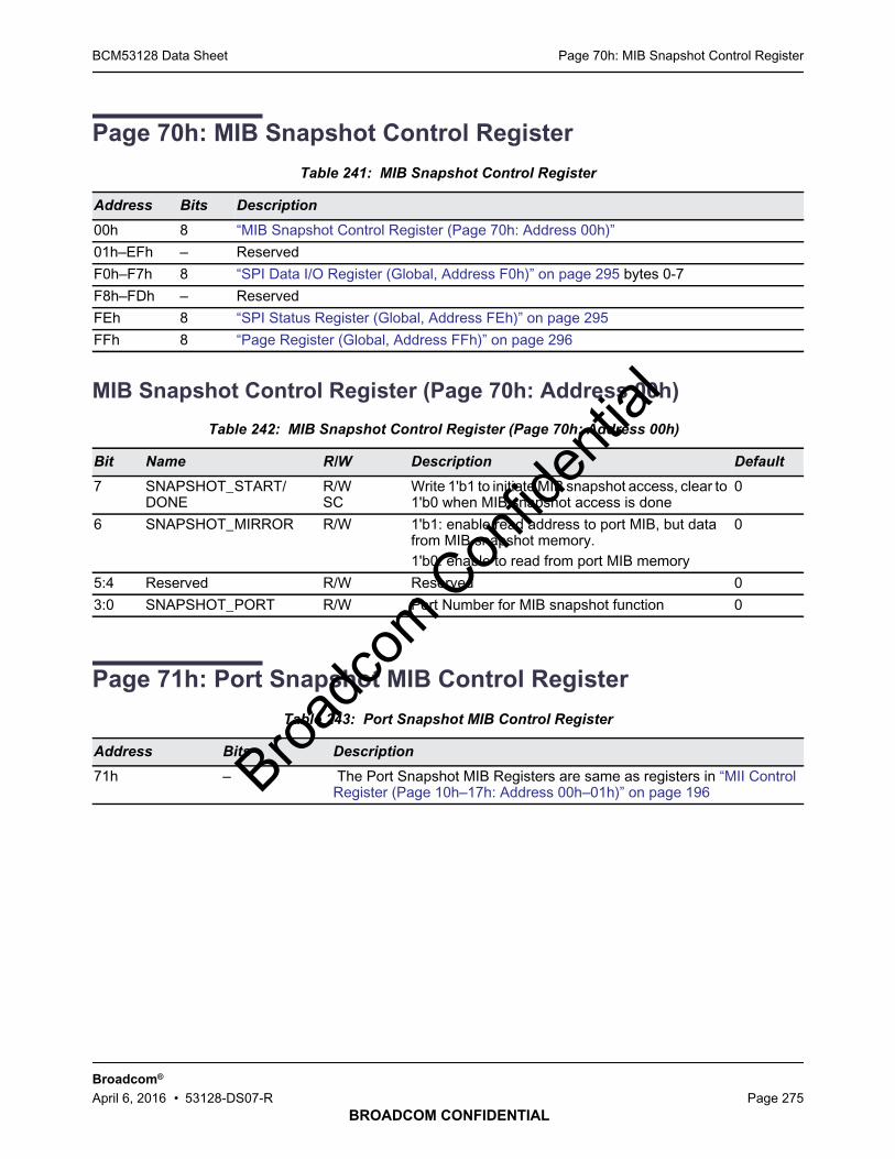
Page 70h: MIB Snapshot Control RegisterBCM53128 Data Sheet
BROADCOM CONFIDENTIAL
Broadcom®
April 6, 2016 • 53128-DS07-R Page 275
Page 70h: MIB Snapshot Control Register
MIB Snapshot Control Register (Page 70h: Address 00h)
Page 71h: Port Snapshot MIB Control Register
Table 241: MIB Snapshot Control Register
Address Bits Description
00h 8 “MIB Snapshot Control Register (Page 70h: Address 00h)”
01h–EFh – Reserved
F0h–F7h 8 “SPI Data I/O Register (Global, Address F0h)” on page 295 bytes 0-7
F8h–FDh – Reserved
FEh 8 “SPI Status Register (Global, Address FEh)” on page 295
FFh 8 “Page Register (Global, Address FFh)” on page 296
Table 242: MIB Snapshot Control Register (Page 70h: Address 00h)
Bit Name R/W Description Default
7 SNAPSHOT_START/DONE
R/WSC
Write 1'b1 to initiate MIB snapshot access, clear to1'b0 when MIB snapshot access is done
0
6 SNAPSHOT_MIRROR R/W 1'b1: enable read address to port MIB, but datafrom MIB snapshot memory.1'b0: enable to read from port MIB memory
0
5:4 Reserved R/W Reserved 0
3:0 SNAPSHOT_PORT R/W Port Number for MIB snapshot function 0
Table 243: Port Snapshot MIB Control Register
Address Bits Description
71h – The Port Snapshot MIB Registers are same as registers in “MII ControlRegister (Page 10h–17h: Address 00h–01h)” on page 196Broadc
om C
onfid
entia
l

Page 72h: Loop Detection RegisterBCM53128 Data Sheet
BROADCOM CONFIDENTIAL
Broadcom®
April 6, 2016 • 53128-DS07-R Page 276
Page 72h: Loop Detection Register
Loop Detection Control Register (Page 72h: Address 00h)
Discovery Frame Timer Control Register (Page 72h: Address 02h)
Table 244: Loop Detection Control Register (Page 72h)
Address Bits Description
00h–01h 16 “Loop Detection Control Register (Page 72h: Address 00h)”
02h 8 “Discovery Frame Timer Control Register (Page 72h: Address 02h)” on page 276
03h–04h 16 “LED Warning Port Map Register (Page 72h: Address 03h)” on page 277
05h–0Ah 48 Module ID 0
0Bh–10h 48 Module ID 1
11h– 16h 48 Loop detect frame SA
17h–EFh – Reserved
F0h–F7h 8 “SPI Data I/O Register (Global, Address F0h)” on page 295, bytes 0–7
F8h–FDh – Reserved
FEh 8 “SPI Status Register (Global, Address FEh)” on page 295
FFh 8 “Page Register (Global, Address FFh)” on page 296
Table 245: Loop Detection Control Registers (Page 72h: Address 00h–01h)
BIt Name R/W Description Default
15:13 Reserved R/W Reserved 0
12 EN_LOOP_DETECT R/W Enable loop detection feature.0 = Disable1 = Enable
Strap
11 LOOP_IMP_SEL R/W Enable IMP loop detection feature.0 = Disable1 = Enable
Strap
10:3 LED_RST_TIMR_CTRL
R/W Number of missed discovery time before LED warningportmap to be reset.
0x4
2 OV_PAUSE_ON R/W 1 = Transmit frame in highest queue even the port is inpause on state.0 = Transmit frame follow the pause state rule.
0x1
1:0 DISCOVERY_FRAME_QUEUE_SEL
R/W Specifies which queue to be put for the received discoveryframe.
0x1
Table 246: Discovery Frame Timer Control Registers (Page 72h: Address 02h)
BIt Name R/W Description Default
7:4 Reserved R/W Reserved 0
Broadc
om C
onfid
entia
l
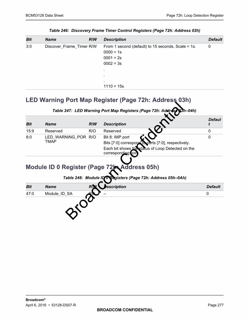
Page 72h: Loop Detection RegisterBCM53128 Data Sheet
BROADCOM CONFIDENTIAL
Broadcom®
April 6, 2016 • 53128-DS07-R Page 277
LED Warning Port Map Register (Page 72h: Address 03h)
Module ID 0 Register (Page 72h: Address 05h)
3:0 Discover_Frame_Timer R/W From 1 second (default) to 15 seconds. Scale = 1s.0000 = 1s0001 = 2s0002 = 3s...1110 = 15s
0
Table 247: LED Warning Port Map Registers (Page 72h: Address 03h–04h)
BIt Name R/W DescriptionDefault
15:9 Reserved R/O Reserved 0
8:0 LED_WARNING_PORTMAP
R/O Bit 8: IMP portBits [7:0] correspond to ports [7:0], respectively.Each bit shows the status of Loop Detected on thecorresponding port.
0
Table 248: Module ID 0 Registers (Page 72h: Address 05h–0Ah)
BIt Name R/W Description Default
47:0 Module_ID_SA RO – 0
Table 246: Discovery Frame Timer Control Registers (Page 72h: Address 02h)
BIt Name R/W Description Default
Broadc
om C
onfid
entia
l
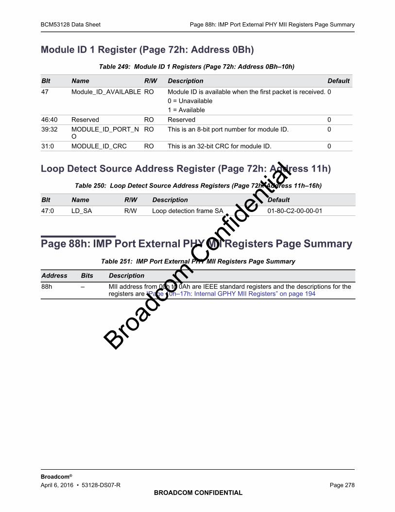
Page 88h: IMP Port External PHY MII Registers Page SummaryBCM53128 Data Sheet
BROADCOM CONFIDENTIAL
Broadcom®
April 6, 2016 • 53128-DS07-R Page 278
Module ID 1 Register (Page 72h: Address 0Bh)
Loop Detect Source Address Register (Page 72h: Address 11h)
Page 88h: IMP Port External PHY MII Registers Page Summary
Table 249: Module ID 1 Registers (Page 72h: Address 0Bh–10h)
BIt Name R/W Description Default
47 Module_ID_AVAILABLE RO Module ID is available when the first packet is received.0 = Unavailable1 = Available
0
46:40 Reserved RO Reserved 0
39:32 MODULE_ID_PORT_NO
RO This is an 8-bit port number for module ID. 0
31:0 MODULE_ID_CRC RO This is an 32-bit CRC for module ID. 0
Table 250: Loop Detect Source Address Registers (Page 72h: Address 11h–16h)
BIt Name R/W Description Default
47:0 LD_SA R/W Loop detection frame SA 01-80-C2-00-00-01
Table 251: IMP Port External PHY MII Registers Page Summary
Address Bits Description
88h – MII address from 00h to 0Ah are IEEE standard registers and the descriptions for theregisters are “Page 10h–17h: Internal GPHY MII Registers” on page 194
Broadc
om C
onfid
entia
l
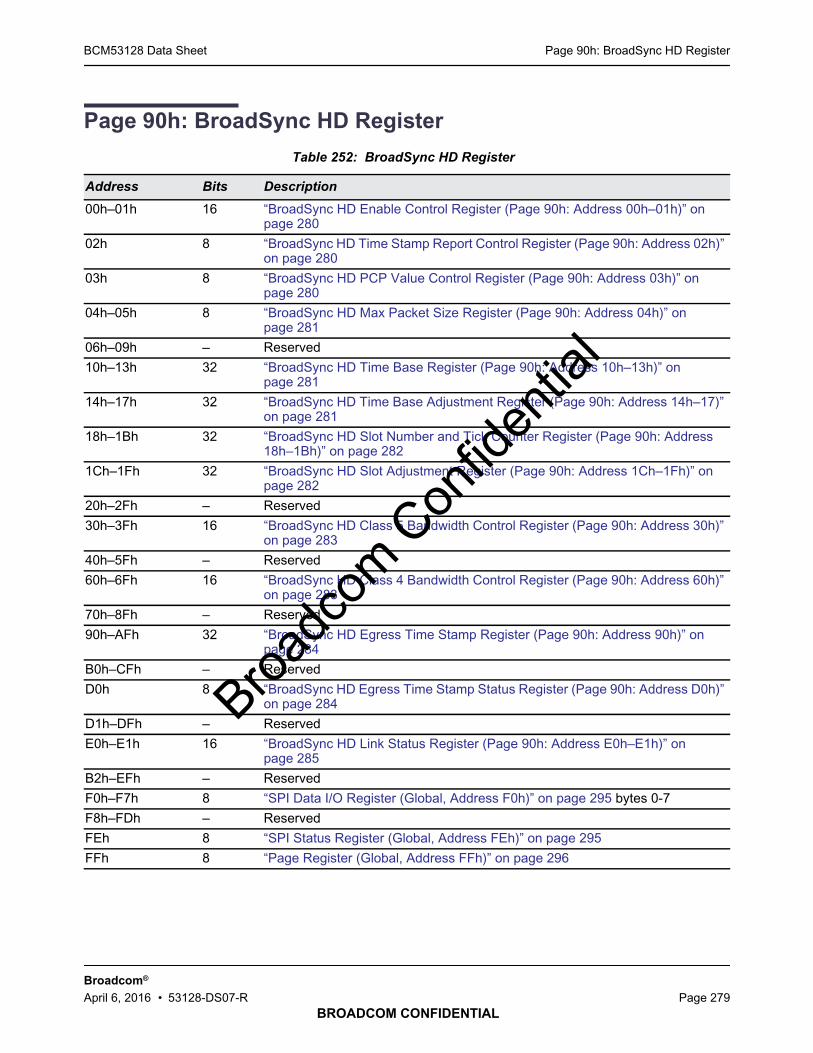
Page 90h: BroadSync HD RegisterBCM53128 Data Sheet
BROADCOM CONFIDENTIAL
Broadcom®
April 6, 2016 • 53128-DS07-R Page 279
Page 90h: BroadSync HD Register
Table 252: BroadSync HD Register
Address Bits Description
00h–01h 16 “BroadSync HD Enable Control Register (Page 90h: Address 00h–01h)” onpage 280
02h 8 “BroadSync HD Time Stamp Report Control Register (Page 90h: Address 02h)”on page 280
03h 8 “BroadSync HD PCP Value Control Register (Page 90h: Address 03h)” onpage 280
04h–05h 8 “BroadSync HD Max Packet Size Register (Page 90h: Address 04h)” onpage 281
06h–09h – Reserved
10h–13h 32 “BroadSync HD Time Base Register (Page 90h: Address 10h–13h)” onpage 281
14h–17h 32 “BroadSync HD Time Base Adjustment Register (Page 90h: Address 14h–17)”on page 281
18h–1Bh 32 “BroadSync HD Slot Number and Tick Counter Register (Page 90h: Address18h–1Bh)” on page 282
1Ch–1Fh 32 “BroadSync HD Slot Adjustment Register (Page 90h: Address 1Ch–1Fh)” onpage 282
20h–2Fh – Reserved
30h–3Fh 16 “BroadSync HD Class 5 Bandwidth Control Register (Page 90h: Address 30h)”on page 283
40h–5Fh – Reserved
60h–6Fh 16 “BroadSync HD Class 4 Bandwidth Control Register (Page 90h: Address 60h)”on page 283
70h–8Fh – Reserved
90h–AFh 32 “BroadSync HD Egress Time Stamp Register (Page 90h: Address 90h)” onpage 284
B0h–CFh – Reserved
D0h 8 “BroadSync HD Egress Time Stamp Status Register (Page 90h: Address D0h)”on page 284
D1h–DFh – Reserved
E0h–E1h 16 “BroadSync HD Link Status Register (Page 90h: Address E0h–E1h)” onpage 285
B2h–EFh – Reserved
F0h–F7h 8 “SPI Data I/O Register (Global, Address F0h)” on page 295 bytes 0-7
F8h–FDh – Reserved
FEh 8 “SPI Status Register (Global, Address FEh)” on page 295
FFh 8 “Page Register (Global, Address FFh)” on page 296
Broadc
om C
onfid
entia
l
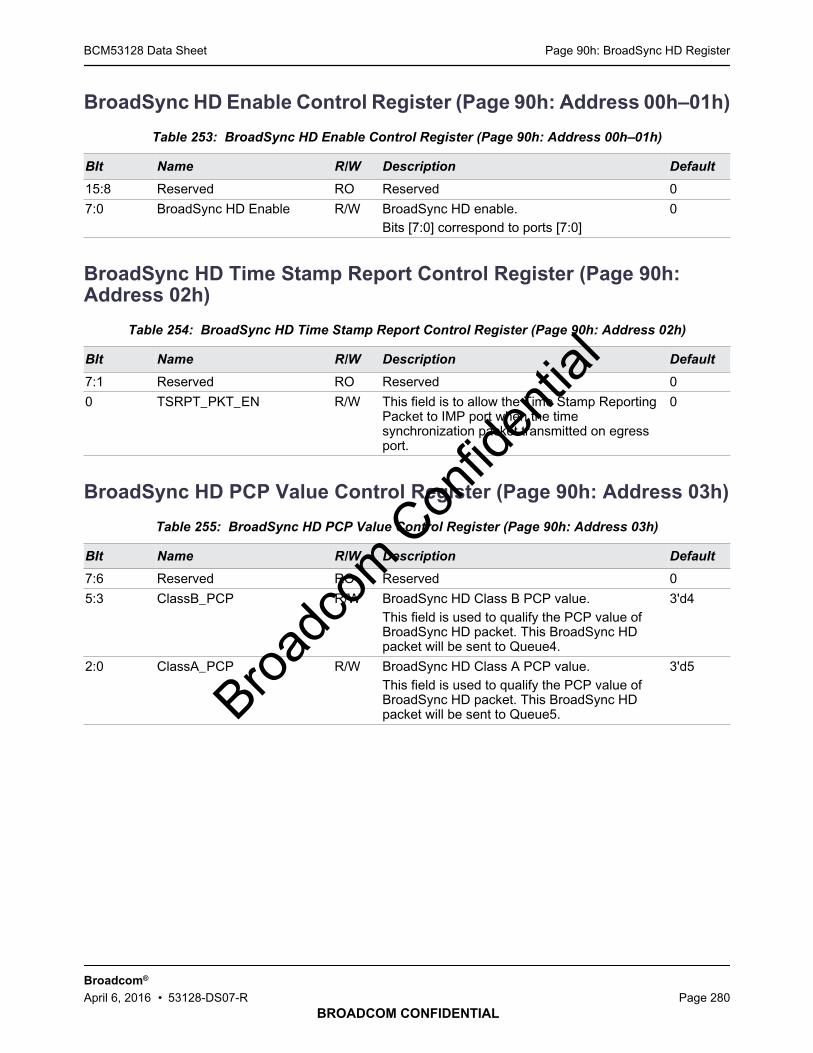
Page 90h: BroadSync HD RegisterBCM53128 Data Sheet
BROADCOM CONFIDENTIAL
Broadcom®
April 6, 2016 • 53128-DS07-R Page 280
BroadSync HD Enable Control Register (Page 90h: Address 00h–01h)
BroadSync HD Time Stamp Report Control Register (Page 90h:Address 02h)
BroadSync HD PCP Value Control Register (Page 90h: Address 03h)
Table 253: BroadSync HD Enable Control Register (Page 90h: Address 00h–01h)
BIt Name R/W Description Default
15:8 Reserved RO Reserved 0
7:0 BroadSync HD Enable R/W BroadSync HD enable.Bits [7:0] correspond to ports [7:0]
0
Table 254: BroadSync HD Time Stamp Report Control Register (Page 90h: Address 02h)
BIt Name R/W Description Default
7:1 Reserved RO Reserved 0
0 TSRPT_PKT_EN R/W This field is to allow the Time Stamp ReportingPacket to IMP port when the timesynchronization packet transmitted on egressport.
0
Table 255: BroadSync HD PCP Value Control Register (Page 90h: Address 03h)
BIt Name R/W Description Default
7:6 Reserved RO Reserved 0
5:3 ClassB_PCP R/W BroadSync HD Class B PCP value.This field is used to qualify the PCP value ofBroadSync HD packet. This BroadSync HDpacket will be sent to Queue4.
3'd4
2:0 ClassA_PCP R/W BroadSync HD Class A PCP value.This field is used to qualify the PCP value ofBroadSync HD packet. This BroadSync HDpacket will be sent to Queue5.
3'd5
Broadc
om C
onfid
entia
l
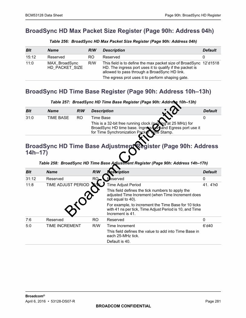
Page 90h: BroadSync HD RegisterBCM53128 Data Sheet
BROADCOM CONFIDENTIAL
Broadcom®
April 6, 2016 • 53128-DS07-R Page 281
BroadSync HD Max Packet Size Register (Page 90h: Address 04h)
BroadSync HD Time Base Register (Page 90h: Address 10h–13h)
BroadSync HD Time Base Adjustment Register (Page 90h: Address14h–17)
Table 256: BroadSync HD Max Packet Size Register (Page 90h: Address 04h)
BIt Name R/W Description Default
15:12 Reserved RO Reserved 0
11:0 MAX_BroadSyncHD_PACKET_SIZE
R/W This field is to define the max packet size of BroadSyncHD. The ingress port uses it to qualify if the packet isallowed to pass through a BroadSync HD link.The egress prot uses it to perform shaping gate.
12’d1518
Table 257: BroadSync HD Time Base Register (Page 90h: Address 10h–13h)
BIt Name R/W Description Default
31:0 TIME BASE RO Time BaseThis is a 32-bit free running clock (running at 25 MHz) forBroadSync HD time base. Ingress port and Egress port use itfor Time Synchronization Packet Time Stamp.
0
Table 258: BroadSync HD Time Base Adjustment Register (Page 90h: Address 14h–17h)
BIt Name R/W Description Default
31:12 Reserved RO Reserved 0
11:8 TIME ADJUST PERIOD R/W Time Adjust PeriodThis field defines the tick numbers to apply theadjusted Time Increment (when Time Increment doesnot equal to 40).For example, to increment the Time Base for 10 tickswith 41 ns per tick, Time Adjust Period is 10, and TimeIncrement is 41.
41. 4’h0
7:6 Reserved RO Reserved 0
5:0 TIME INCREMENT R/W Time IncrementThis field defines the value to add into Time Base ineach 25-MHz tick.Default is 40.
6’d40
Broadc
om C
onfid
entia
l

Page 90h: BroadSync HD RegisterBCM53128 Data Sheet
BROADCOM CONFIDENTIAL
Broadcom®
April 6, 2016 • 53128-DS07-R Page 282
BroadSync HD Slot Number and Tick Counter Register (Page 90h:Address 18h–1Bh)
BroadSync HD Slot Adjustment Register (Page 90h: Address 1Ch–1Fh)
Table 259: BroadSync HD Slot Number and Tick Counter Register (Page 90h: Address 18h–1Bh)
BIt Name R/W Description Default
31:28 Reserved RO Reserved 0
27:16 TICK COUNTER R/W Tick CounterThis is the tick counter which defines when willSlot Number increment. It runs from 1 to 3125 (or3124, or 3126, depends on “BroadSync HD SlotNumber and Tick Counter Register (Page 90h:Address 18h–1Bh)” on page 282 setting) under25 MHz.
12’h0
15:5 Reserved RO Reserved 0
4:0 SLOT NUMBER R/W This field specifies the Slot Number forBroadSync HD.
8’h0
Table 260: BroadSync HD Slot Adjustment Register (Page 90h: Address 1Ch–1Fh)
BIt Name R/W Description Default
31:18 Reserved RO Reserved 0
17:16 MACRO SLOT PERIOD R/W Macro Slot PeriodThis field defines the slot time of a macro slot forClass 4 traffic.00 = 1 ms01 = 2 ms10 = 4 ms11 = ReservedClass 5 traffic slot time is always 125s period.
2’h0
15:12 Reserved RO Reserved 0
11:8 SLOT ADJUST PERIOD R/W Slot Adjust PeriodThis field defines the number of slots to apply thealterable slot adjustment.
8’h0
7:2 Reserved RO Reserved 0
1:0 SLOT ADJUSTMENT R/W Slot AdjustmentThis field defines when the slot number counterincrement by 1. Default is 40.00 = Slot Number increased by 1 when tickcounter rolls over 3125.01 = 312610 = 312411 = Reserved
2’h0
Broadc
om C
onfid
entia
l

Page 90h: BroadSync HD RegisterBCM53128 Data Sheet
BROADCOM CONFIDENTIAL
Broadcom®
April 6, 2016 • 53128-DS07-R Page 283
BroadSync HD Class 5 Bandwidth Control Register (Page 90h:Address 30h)
.
BroadSync HD Class 4 Bandwidth Control Register (Page 90h:Address 60h)
.
Table 261: BroadSync HD Class 5 Bandwidth Control Register Address Summary
Address Description
30h–31h Port 0
32h–33h Port 1
34h–35h Port 2
36h–37h Port 3
38h–39h Port 4
3Ah-3Bh Port 5
3Ch–3Dh Port 6
3Eh-3Fh Port 7
Table 262: BroadSync HD Class 5 Bandwidth Control Register (Page 90h: Address 30h–31h, 32h–33h,34h–35h, 36h–37h, 38h–39h)
BIt Name R/W Description Default
15 C5_WINDOW R/W The purpose is to control the credit carry-over underdifferent link speed. For a 100M link, the 125-s slot is toosmall such that BroadSync HD packet could easily “slipslot”, so the credit carry-over should be allowed. For a 1Glink, 125-s slot is reasonably big such that the BWreservation could be done in a conservative way to prevent“slot slipping”, so credit carry-over is not needed.
1’b0
14 Reserved RO Reserved 0
13:0 C5_BANDWIDTH R/W This field defines the byte count allowed for Class 5 traffictransmission within a slot time.
14’h0
Table 263: BroadSync HD Class 4 Bandwidth Control Register Address Summary
Address Description
60h–61h Port 0
62h–63h Port 1
64h–65h Port 2
66h–67h Port 3
68h–69h Port 4
6Ah-6Bh Port 5
6Ch–6Dh Port 6
6Eh-6Fh Port 7
Broadc
om C
onfid
entia
l

Page 90h: BroadSync HD RegisterBCM53128 Data Sheet
BROADCOM CONFIDENTIAL
Broadcom®
April 6, 2016 • 53128-DS07-R Page 284
BroadSync HD Egress Time Stamp Register (Page 90h: Address 90h).
BroadSync HD Egress Time Stamp Status Register (Page 90h:Address D0h)
Table 264: BroadSync HD Class 4 Bandwidth Control Register (Page 90h: Address 60h–61h, 62h–63h,64h–65h, 66h–67h, 68h–69h)
BIt Name R/W Description Default
15:14 Reserved RO Reserved 0
13:0 C4_BANDWIDTH R/W This field defines the byte count allowed forClass 4 traffic transmission within a slot time.
14’h0
Table 265: BroadSync HD Egress Time Stamp Register Address Summary
Address Description
90h–93h Port 0
94h–97h Port 1
98h–9Bh Port 2
9Ch–9Fh Port 3
A0h–A3h Port 4
A4h-A7h Port 5
A8h–ABh Port 6
ACh-AFh Port 7
Table 266: BroadSync HD Egress Time Stamp Register (Page 90h: Address 90h–93h, 94h–97h, 98h–9Bh,9Ch–9Fh, A0h–A3h, A4h–A7h)
BIt Name R/W Description Default
31:0 EGRESS_TS R Egress Time Synchronous Packet Time StampThis field reports the time stamp of egress time synchronouspacket.It uses 32-bit time base as time stamping. The time between thedeparture of first byte of MAC DA and the time stamping pointshould be constant.
32’h0
Table 267: BroadSync HD Egress Time Stamp Status Register (Page 90h: Address D0h)
BIt Name R/W Description Default
7:0 VALID STATUS RO Valid Status8-bit field indicating the valid status for each “BroadSync HDEgress Time Stamp Register (Page 90h: Address 90h)” onpage 284. When “BroadSync HD Egress Time Stamp Register(Page 90h: Address 90h)” is read out by SPI, the valid status willbe cleared, respectively.
8’h0
Broadc
om C
onfid
entia
l
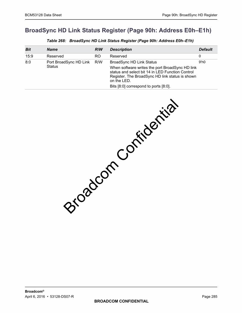
Page 90h: BroadSync HD RegisterBCM53128 Data Sheet
BROADCOM CONFIDENTIAL
Broadcom®
April 6, 2016 • 53128-DS07-R Page 285
BroadSync HD Link Status Register (Page 90h: Address E0h–E1h)
Table 268: BroadSync HD Link Status Register (Page 90h: Address E0h–E1h)
Bit Name R/W Description Default
15:9 Reserved RO Reserved 0
8:0 Port BroadSync HD LinkStatus
R/W BroadSync HD Link StatusWhen software writes the port BroadSync HD linkstatus and select bit 14 in LED Function ControlRegister. The BroadSync HD link status is shownon the LED.Bits [8:0] correspond to ports [8:0].
9'h0
Broadc
om C
onfid
entia
l

Page 91h: Traffic Remarking RegisterBCM53128 Data Sheet
BROADCOM CONFIDENTIAL
Broadcom®
April 6, 2016 • 53128-DS07-R Page 286
Page 91h: Traffic Remarking Register
Traffic Remarking Control Register (Page 91h: Address 00h)
Table 269: Traffic Remarking Register
Address Bits Description
00h–03h 32 “Traffic Remarking Control Register (Page 91h: Address 00h)”
04h–0Fh – Reserved
10h-57h 32 “Egress Non-BroadSync HD Packet TC to PCP Mapping Register (Page 91h:Address 10h)” on page 287
58h–EFh – Reserved
F0h–F7h 8 “SPI Data I/O Register (Global, Address F0h)” on page 295, bytes 0–7
F8h–FDh – Reserved
FEh 8 “SPI Status Register (Global, Address FEh)” on page 295
FFh 8 “Page Register (Global, Address FFh)” on page 296
Table 270: Traffic Remarking Control Register (Page 91h: Address 00h)
BIt Name R/W Description Default
31:25 Reserved RO Reserved 0
24:16 PCP_REMARKING_EN R/W PCP Remarking EnableBit 24: IMP portBits[23:16] correspond to ports [7:0], respectively
0
15:9 Reserved R/W Reserved –
8:0 Reserved R/W Reserved 0
Broadc
om C
onfid
entia
l

Page 91h: Traffic Remarking RegisterBCM53128 Data Sheet
BROADCOM CONFIDENTIAL
Broadcom®
April 6, 2016 • 53128-DS07-R Page 287
Egress Non-BroadSync HD Packet TC to PCP Mapping Register(Page 91h: Address 10h)
Table 271: Egress Non-BroadSync HD Packet TC to PCP Mapping Register Address Summary
Address Description
10h-17h Port 0
18h-1Fh Port 1
20h-27h Port 2
28h-2Fh Port 3
30h-37h Port 4
38h-3Fh Port 5
40h-47h Port 6
48h-4Fh Port 7
50h-57h IMP
Table 272: Egress Non-BroadSync HD Packet TC to PCP Mapping Register (Page 91h: Address 10h–17h, 18h–1Fh, 20h–27h, 28h–2Fh, 30h–37h, 38h–3Fh, 50h-57h)
Bit Name R/W Description Default
63:32 Reserved R/W Reserved 4'b1111
31:28 {CFI,PCP} for TC = 7 R/W The {CFI,PCP} field for TC = 7 4'b0111
27:24 {CFI,PCP} for TC = 6 R/W The {CFI,PCP} field for TC = 6 4'b0110
23:20 {CFI,PCP} for TC = 5 R/W The {CFI,PCP} field for TC = 5 4'b0101
19:16 {CFI,PCP} for TC = 4 R/W The {CFI,PCP} field for TC = 4 4'b0100
15:12 {CFI,PCP} for TC = 3 R/W The {CFI,PCP} field for TC = 3 4'b0011
11:8 {CFI,PCP} for TC = 2 R/W The {CFI,PCP} field for TC = 2 4'b0010
7:4 {CFI,PCP} for TC = 1 R/W The {CFI,PCP} field for TC = 1 4'b0001
3:0 {CFI,PCP} for TC = 0 R/W The {CFI,PCP} field for TC = 0 4'b0000
Broadc
om C
onfid
entia
l
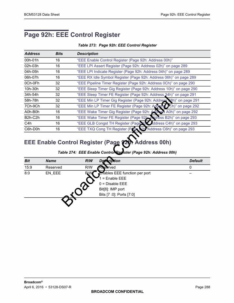
Page 92h: EEE Control RegisterBCM53128 Data Sheet
BROADCOM CONFIDENTIAL
Broadcom®
April 6, 2016 • 53128-DS07-R Page 288
Page 92h: EEE Control Register
EEE Enable Control Register (Page 92h: Address 00h)
Table 273: Page 92h: EEE Control Register
Address Bits Description
00h-01h 16 “EEE Enable Control Register (Page 92h: Address 00h)”
02h-03h 16 “EEE LPI Assert Register (Page 92h: Address 02h)” on page 289
04h-05h 16 “EEE LPI Indicate Register (Page 92h: Address 04h)” on page 289
06h-07h 16 “EEE RX Idle Symbol Register (Page 92h: Address 06h)” on page 289
0Ch-0Fh 32 “EEE Pipeline Timer Register (Page 92h: Address 0Ch)” on page 290
10h-30h 32 “EEE Sleep Timer Gig Register (Page 92h: Address 10h)” on page 290
34h-54h 32 “EEE Sleep Timer FE Register (Page 92h: Address 34h)” on page 291
58h-78h 32 “EEE Min LP Timer Gig Register (Page 92h: Address 58h)” on page 291
7Ch-9Ch 32 “EEE Min LP Timer FE Register (Page 92h: Address 7Ch)” on page 292
A0h-B0h 16 “EEE Wake Timer Gig Register (Page 92h: Address A0h)” on page 292
B2h-C2h 16 “EEE Wake Timer FE Register (Page 92h: Address B2h)” on page 293
C4h 16 “EEE GLB Congst TH Register (Page 92h: Address C4h)” on page 293
C6h-D0h 16 “EEE TXQ Cong TH Register (Page 92h: Address C6h)” on page 293
Table 274: EEE Enable Control Register (Page 92h: Address 00h)
Bit Name R/W Description Default
15:9 Reserved R/W Reserved 0
8:0 EN_EEE R/W Enables EEE function per port1 = Enable EEE0 = Disable EEEBit[8]: IMP portBits [7 :0]: Ports [7:0]
–
Broadc
om C
onfid
entia
l
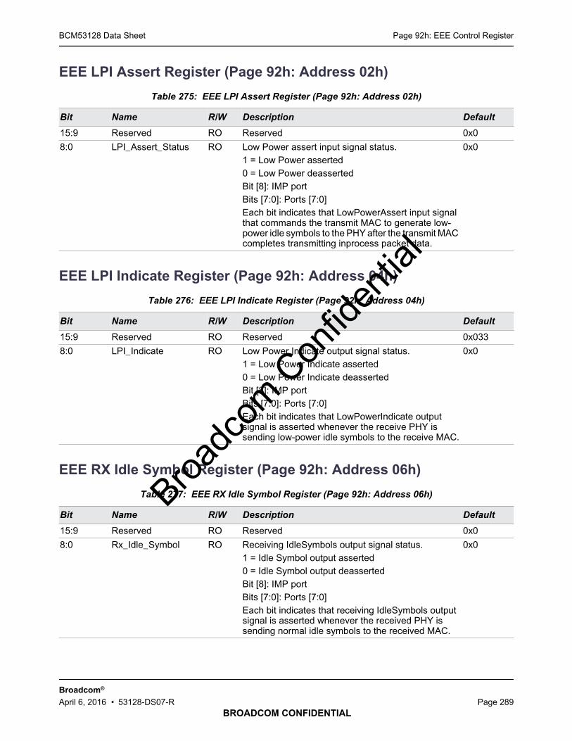
Page 92h: EEE Control RegisterBCM53128 Data Sheet
BROADCOM CONFIDENTIAL
Broadcom®
April 6, 2016 • 53128-DS07-R Page 289
EEE LPI Assert Register (Page 92h: Address 02h)
EEE LPI Indicate Register (Page 92h: Address 04h)
EEE RX Idle Symbol Register (Page 92h: Address 06h)
Table 275: EEE LPI Assert Register (Page 92h: Address 02h)
Bit Name R/W Description Default
15:9 Reserved RO Reserved 0x0
8:0 LPI_Assert_Status RO Low Power assert input signal status.1 = Low Power asserted0 = Low Power deassertedBit [8]: IMP portBits [7:0]: Ports [7:0]Each bit indicates that LowPowerAssert input signalthat commands the transmit MAC to generate low-power idle symbols to the PHY after the transmit MACcompletes transmitting inprocess packet data.
0x0
Table 276: EEE LPI Indicate Register (Page 92h: Address 04h)
Bit Name R/W Description Default
15:9 Reserved RO Reserved 0x033
8:0 LPI_Indicate RO Low Power Indicate output signal status.1 = Low Power Indicate asserted0 = Low Power Indicate deassertedBit [8]: IMP portBits [7:0]: Ports [7:0]Each bit indicates that LowPowerIndicate outputsignal is asserted whenever the receive PHY issending low-power idle symbols to the receive MAC.
0x0
Table 277: EEE RX Idle Symbol Register (Page 92h: Address 06h)
Bit Name R/W Description Default
15:9 Reserved RO Reserved 0x0
8:0 Rx_Idle_Symbol RO Receiving IdleSymbols output signal status.1 = Idle Symbol output asserted0 = Idle Symbol output deassertedBit [8]: IMP portBits [7:0]: Ports [7:0]Each bit indicates that receiving IdleSymbols outputsignal is asserted whenever the received PHY issending normal idle symbols to the received MAC.
0x0
Broadc
om C
onfid
entia
l

Page 92h: EEE Control RegisterBCM53128 Data Sheet
BROADCOM CONFIDENTIAL
Broadcom®
April 6, 2016 • 53128-DS07-R Page 290
EEE Pipeline Timer Register (Page 92h: Address 0Ch)
EEE Sleep Timer Gig Register (Page 92h: Address 10h)
Table 278: EEE Pipeline Timer Register (Page 92h: Address 0Ch)
Bit Name R/W Description Default
31:0 Pipeline Timer R/W EEE pipeline delay timer load value.The unit is system clock rate (e.g., if system clock =100 MHz, unit = 10 nsec).
0x20
Table 279: EEE Sleep Timer Gig Register (Page 92h: Address 10h)
Address Description
10h – 13h Port 0
14h – 17h Port 1
18h – 1Bh Port 2
1Ch – 1Fh Port 3
20h – 23h Port 4
24h – 27h Port 5
28h – 2Bh Port 6
2Ch – 2Fh Port 7
30h – 33h IMP
Table 280: EEE Sleep Timer Gig Register (Page 92h: Address 10h)
Bit Name R/W Description Default
31:0 Sleep Timer Gig R/W EEE sleep delay timer load value for 1G operation.The unit is 1 sec.
0x4
Table 281: EEE Sleep Timer FE Register (Page 92h: Address 34h)
Address Description
34h – 37h Port 0
38h – 3Bh Port 1
3Ch – 3Fh Port 2
40h – 43h Port 3
44h – 47h Port 4
48h – 4Bh Port 5
4Ch – 4Fh Port 6
50h – 53h Port 7
54h – 57h IMP
Broadc
om C
onfid
entia
l
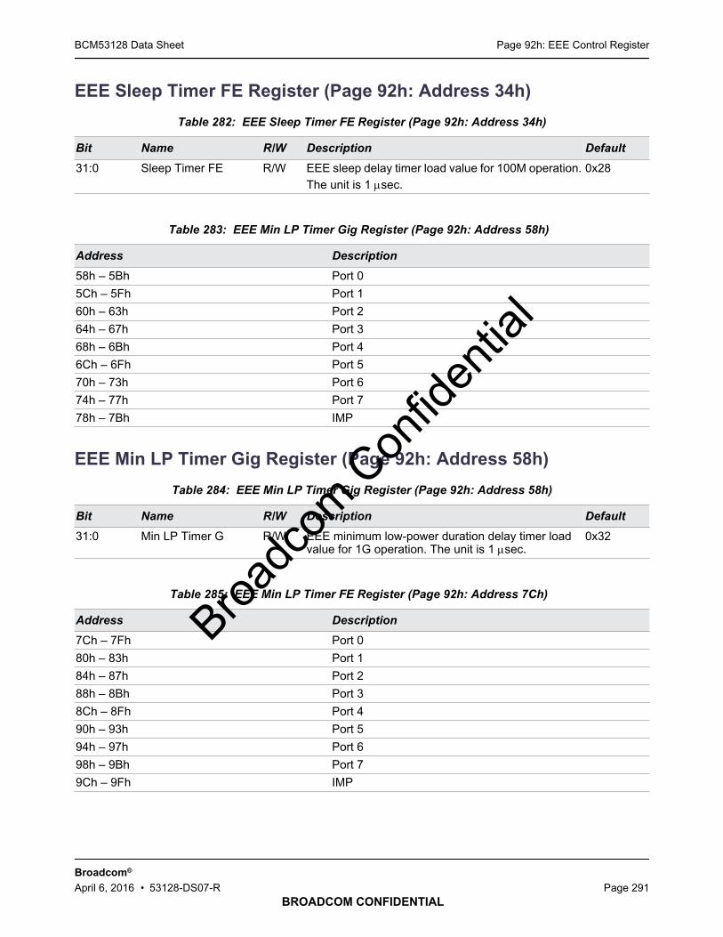
Page 92h: EEE Control RegisterBCM53128 Data Sheet
BROADCOM CONFIDENTIAL
Broadcom®
April 6, 2016 • 53128-DS07-R Page 291
EEE Sleep Timer FE Register (Page 92h: Address 34h)
EEE Min LP Timer Gig Register (Page 92h: Address 58h)
Table 282: EEE Sleep Timer FE Register (Page 92h: Address 34h)
Bit Name R/W Description Default
31:0 Sleep Timer FE R/W EEE sleep delay timer load value for 100M operation.The unit is 1 sec.
0x28
Table 283: EEE Min LP Timer Gig Register (Page 92h: Address 58h)
Address Description
58h – 5Bh Port 0
5Ch – 5Fh Port 1
60h – 63h Port 2
64h – 67h Port 3
68h – 6Bh Port 4
6Ch – 6Fh Port 5
70h – 73h Port 6
74h – 77h Port 7
78h – 7Bh IMP
Table 284: EEE Min LP Timer Gig Register (Page 92h: Address 58h)
Bit Name R/W Description Default
31:0 Min LP Timer G R/W EEE minimum low-power duration delay timer loadvalue for 1G operation. The unit is 1 sec.
0x32
Table 285: EEE Min LP Timer FE Register (Page 92h: Address 7Ch)
Address Description
7Ch – 7Fh Port 0
80h – 83h Port 1
84h – 87h Port 2
88h – 8Bh Port 3
8Ch – 8Fh Port 4
90h – 93h Port 5
94h – 97h Port 6
98h – 9Bh Port 7
9Ch – 9Fh IMP
Broadc
om C
onfid
entia
l
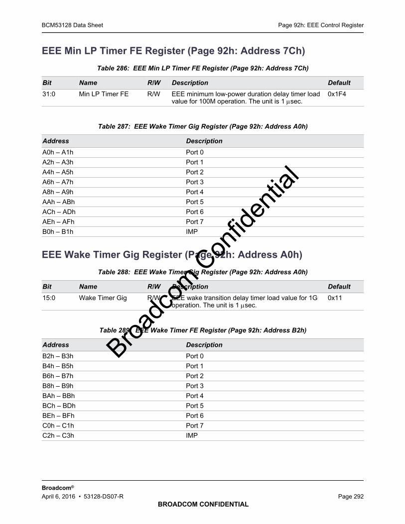
Page 92h: EEE Control RegisterBCM53128 Data Sheet
BROADCOM CONFIDENTIAL
Broadcom®
April 6, 2016 • 53128-DS07-R Page 292
EEE Min LP Timer FE Register (Page 92h: Address 7Ch)
EEE Wake Timer Gig Register (Page 92h: Address A0h)
Table 286: EEE Min LP Timer FE Register (Page 92h: Address 7Ch)
Bit Name R/W Description Default
31:0 Min LP Timer FE R/W EEE minimum low-power duration delay timer loadvalue for 100M operation. The unit is 1 sec.
0x1F4
Table 287: EEE Wake Timer Gig Register (Page 92h: Address A0h)
Address Description
A0h – A1h Port 0
A2h – A3h Port 1
A4h – A5h Port 2
A6h – A7h Port 3
A8h – A9h Port 4
AAh – ABh Port 5
ACh – ADh Port 6
AEh – AFh Port 7
B0h – B1h IMP
Table 288: EEE Wake Timer Gig Register (Page 92h: Address A0h)
Bit Name R/W Description Default
15:0 Wake Timer Gig R/W EEE wake transition delay timer load value for 1Goperation. The unit is 1 sec.
0x11
Table 289: EEE Wake Timer FE Register (Page 92h: Address B2h)
Address Description
B2h – B3h Port 0
B4h – B5h Port 1
B6h – B7h Port 2
B8h – B9h Port 3
BAh – BBh Port 4
BCh – BDh Port 5
BEh – BFh Port 6
C0h – C1h Port 7
C2h – C3h IMP
Broadc
om C
onfid
entia
l

Page 92h: EEE Control RegisterBCM53128 Data Sheet
BROADCOM CONFIDENTIAL
Broadcom®
April 6, 2016 • 53128-DS07-R Page 293
EEE Wake Timer FE Register (Page 92h: Address B2h)
EEE GLB Congst TH Register (Page 92h: Address C4h)
EEE TXQ Cong TH Register (Page 92h: Address C6h)
Table 290: EEE Wake Timer FE Register (Page 92h: Address B2h)
Bit Name R/W Description Default
15:0 Wake Timer FE R/W EEE wake transition delay timer load value for 100Moperation. The unit is 1 sec.
0x24
Table 291: EEE GLB Congst TH Register (Page 92h: Address C4h)
Bit Name R/W Description Default
15:11 Reserved RO Reserved 0x0
10:0 GLB_CONG_TH R/W EEE Global packet buffer congestion threshold. If thisthreshold is set to zero, then EEE is effectivelydisabled. If this threshold is set equal to or greaterthan 768 (the number of cells implemented in thepacket buffer), then protections against packet lossare disable.The unit is “Buffer Cell Size”: 256-byte cell.
0x1a0
Table 292: EEE TXQ CONG TH Register (Page 92h: Address C6h)
Address Description
C6h C7hEEE TXQ 0 CONG TH Register
C8h C9hEEE TXQ 1 CONG TH Register
CAh CBhEEE TXQ 2 CONG TH Register
CCh CDhEEE TXQ 3 CONG TH Register
CEh CFhEEE TXQ 4 CONG TH Register
D0h D1hEEE TXQ 5 CONG TH Register
Table 293: EEE TXQ Cong TH Register (Page 92h: Address C6h)
Bit Name R/W Description Default
15:11 Reserved RO Reserved 0x0
Broadc
om C
onfid
entia
l

Page 92h: EEE Control RegisterBCM53128 Data Sheet
BROADCOM CONFIDENTIAL
Broadcom®
April 6, 2016 • 53128-DS07-R Page 294
10:0 GLB_CONG_TH R/W EEE TXQ packet buffer congestion threshold.• If this threshold is set to zero, then EEE for queue
N is effectively disabled.• If this threshold is set equal to or greater than 768
(the number of cells implemented in the packetbuffer), then protections against packet loss aredisabled.
The unit is “Buffer Cell Size”: 256-byte cell.EEE TXQ0: 0x64EEE TXQ1: 0x64EEE TXQ2: 0x64EEE TXQ3: 0x1EEE TXQ4: 0x1EEE TXQ5: 0x1
Table 293: EEE TXQ Cong TH Register (Page 92h: Address C6h)
Bit Name R/W Description Default
Broadc
om C
onfid
entia
l

Global RegistersBCM53128 Data Sheet
BROADCOM CONFIDENTIAL
Broadcom®
April 6, 2016 • 53128-DS07-R Page 295
Global Registers
SPI Data I/O Register (Global, Address F0h)
SPI Status Register (Global, Address FEh)
Table 294: Global Registers (Maps to All Pages)
Address Bits Description
F0h 8 “SPI Data I/O Register (Global, Address F0h)”, 0
F1h 8 “SPI Data I/O Register (Global, Address F0h)”, 1
F2h 8 “SPI Data I/O Register (Global, Address F0h)” on page 295, 2
F3h 8 “SPI Data I/O Register (Global, Address F0h)” on page 295, 3
F4h 8 “SPI Data I/O Register (Global, Address F0h)” on page 295, 4
F5h 8 “SPI Data I/O Register (Global, Address F0h)” on page 295, 5
F6h 8 “SPI Data I/O Register (Global, Address F0h)” on page 295, 6
F7h 8 “SPI Data I/O Register (Global, Address F0h)” on page 295, 7
F8–FDh – Reserved
FEh 8 “SPI Status Register (Global, Address FEh)” on page 295
FFh 8 “Page Register (Global, Address FFh)” on page 296
Table 295: SPI Data I/O Register (Maps to All Registers, Address F0h–F7h)
Bit Name R/W Description Default
7:0 SPI Data I/O R/W SPI data bytes [7:0] 0
Table 296: SPI Status Register (Maps to All Registers, Address FEh)
Bit Name R/W Description Default
7 SPIF RO SPI read/write complete flag 0
6 Reserved RO Reserved 0
5 RACK RO(SC)
SPI read data ready acknowledgement (self-clearing) 0
4:2 Reserved RO Reserved 0
1 Reserved RO Reserved 0
0 Reserved RO Reserved 0
Broadc
om C
onfid
entia
l

Global RegistersBCM53128 Data Sheet
BROADCOM CONFIDENTIAL
Broadcom®
April 6, 2016 • 53128-DS07-R Page 296
Page Register (Global, Address FFh)
Table 297: Page Register (Maps to All Registers, Address FFh)
Bit Name R/W Description Default
7:0 PAGE_REG R/W The binary value determines the value of the accessedregister page.
0
Broadc
om C
onfid
entia
l

Electrical CharacteristicsBCM53128 Data Sheet
BROADCOM CONFIDENTIAL
Broadcom®
April 6, 2016 • 53128-DS07-R Page 297
Section 8: Electrical Characteristics
Absolute Maximum Ratings
Recommended Operating Conditions
Table 298: Absolute Maximum Ratings
Symbol Parameter and Pins Minimum Maximum Units
– Supply voltage: PLL_AVDD, DVDD, AVDDL GND–0.3 1.32 V
– Supply voltage: OVDD2, AVDDH, OVDD, XTAL_AVDD GND–0.3 3.63 V
II Input current – – mA
TSTG Storage temperature –40 +125 C
VESD Electrostatic discharge – 2000 V
– Input voltage: digital input pins – – V
Note: These specifications indicate levels where permanent damage to the device may occur. Functionaloperation is not guaranteed under these conditions. Operation at absolute maximum conditions for extendedperiods may adversely affect long-term reliability of the device.
Table 299: Recommended Operating Conditions
Symbol Parameter Pins Minimum Maximum Units
VDD Supply voltage AVDDL, DVDD, PLL_AVDD 1.14 1.26 V
OVDD2, AVDDH, XTAL_AVDD 3.14 3.47 V
– – – V
– – – V
VIH High-level input voltage All digital inputs 2.0 – V
VIL Low-level input voltage All digital inputs – 0.8 V
TA Ambient operatingtemperature
– 0 70 CBroadc
om C
onfid
entia
l

Electrical CharacteristicsBCM53128 Data Sheet
BROADCOM CONFIDENTIAL
Broadcom®
April 6, 2016 • 53128-DS07-R Page 298
Electrical Characteristics
Table 300: Electrical Characteristics
Symbol Parameter Pins Conditions Minimum Typical Maximum Units
IDD Maximum supplycurrent (for GMII/RvMII/MIIoperation)
1.2V power rail Estimated – 1130 – mA
3.3V power rail Estimated – 496 – mA
OVDD (3.3V for GMII/RvMII/MII)
Estimated – 36 – mA
IDD Maximum supplycurrent (for RGMIIoperation)
1.2V power rail Estimated – 1130 – mA
3.3V power rail Estimated – 496 – mA
2.5V power rail Estimated – 26 – mA
1.5V power rail – – – – mA
VOH High-leveloutput voltage
Digital output pins at 3.3V IOH = 8 mA 2.1 – – V
Digital output pins at 2.5V IOH = 8 mA 2.0 – – V
Digital output pins at 1.5V IOH = 8 mA 1.1 – – V
VOL Low-leveloutput voltage
Digital output pins at 3.3V IOL = 8 mA – – 0.5 V
Digital output pins at 2.5V IOL = 8 mA – – 0.4 V
Digital output pins at 1.5V IOL = 8 mA – – 0.4 V
VIH High-levelinput voltage
Digital input pins at 3.3Vand 2.5V
– 1.7 – – V
Digital input pins at 1.5V – 0.85 – – V
XTALI – 2.0 – – V
VIL Low-levelinput voltage
Digital input pins at 3.3V – – – 0.9 V
Digital input pins at 2.5V – – – 0.7 V
Digital input pins at 1.5V – – – 0.65 V
XTALI – – – 0.8 V
II Input current Digital inputsw/ pull-up resistors
– – – – µA
Digital inputsw/ pull-up resistors
– – – – µA
Digital inputsw/ pull-down resistors
– – – – µA
Digital inputsw/ pull-down resistors
– – – – µA
All other digital inputs – – – – µA
Broadc
om C
onfid
entia
l

Timing CharacteristicsBCM53128 Data Sheet
BROADCOM CONFIDENTIAL
Broadcom®
April 6, 2016 • 53128-DS07-R Page 299
Section 9: Timing Characteristics
Reset and Clock Timing
Figure 49: Reset and Clock Timing
Table 301: Reset and Clock Timing
Description Parameter Minimum Typical Maximum
XTALI period t101 39.998 ns 40 ns 40.002 ns
XTALI high time t102 18 ns – 22 ns
XTALI low time t103 18 ns – 22 ns
RESET low pulse duration t104 80 ms 100 ms –
RESET rise time t105 – – 25 ns
Configuration valid setup to RESET rising t107 100 ns – –
Configuration valid hold from RESET rising t108 – – 100 ns
Hardware initialization is complete. All the strap pinvalues are clocked in, and the internal registers canbe accessed.
t109 5 ms before the registers can be accessed
Power Rails
XTALI
RESET
ConfigurationStrap Signals Valid
t104
t101 t103
t106
t102t107 t108
t105
t109
Broadc
om C
onfid
entia
l
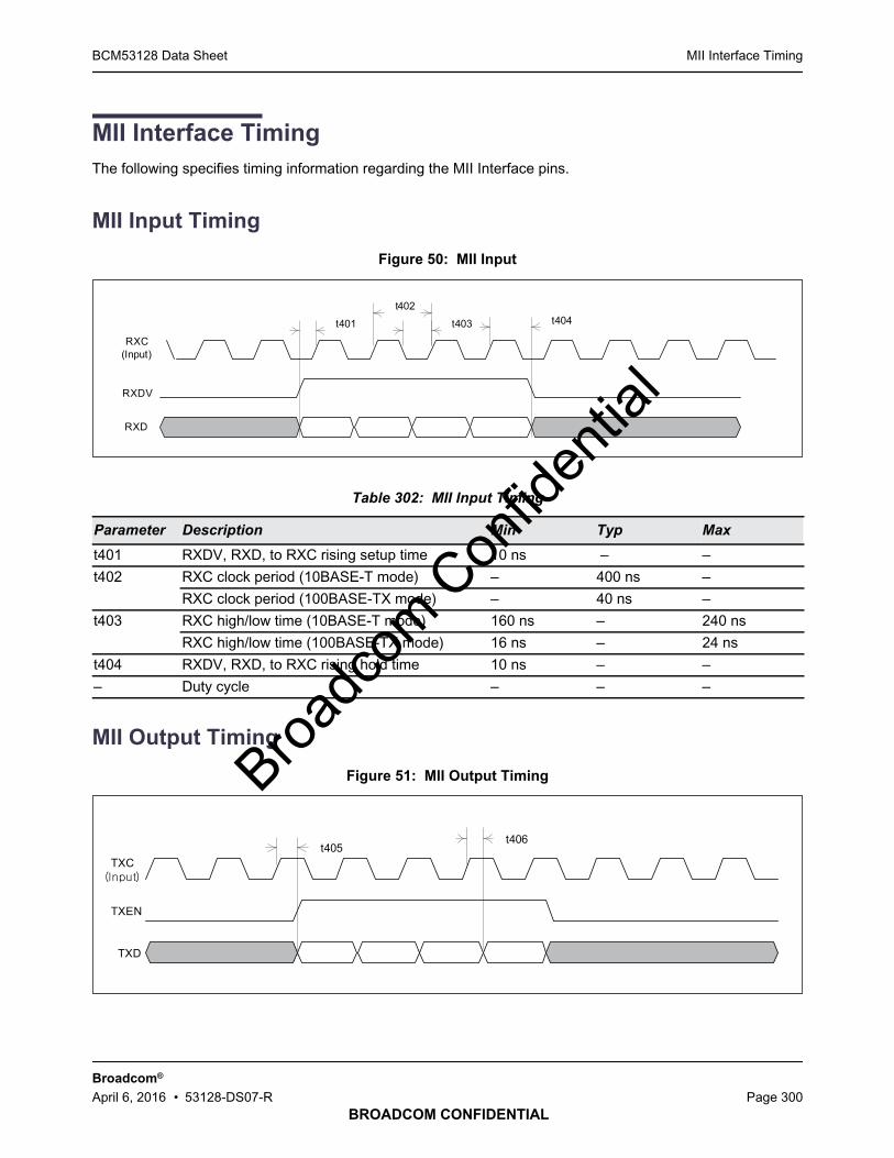
MII Interface TimingBCM53128 Data Sheet
BROADCOM CONFIDENTIAL
Broadcom®
April 6, 2016 • 53128-DS07-R Page 300
MII Interface Timing
The following specifies timing information regarding the MII Interface pins.
MII Input Timing
Figure 50: MII Input
MII Output Timing
Figure 51: MII Output Timing
Table 302: MII Input Timing
Parameter Description Min Typ Max
t401 RXDV, RXD, to RXC rising setup time 10 ns – –
t402 RXC clock period (10BASE-T mode) – 400 ns –
RXC clock period (100BASE-TX mode) – 40 ns –
t403 RXC high/low time (10BASE-T mode) 160 ns – 240 ns
RXC high/low time (100BASE-TX mode) 16 ns – 24 ns
t404 RXDV, RXD, to RXC rising hold time 10 ns – –
– Duty cycle – – –
RXDV
RXD
t401
t402
t403 t404
RXC(Input)
TXC
TXEN
TXD
t405t406
Broadc
om C
onfid
entia
l

TMII Interface TimingBCM53128 Data Sheet
BROADCOM CONFIDENTIAL
Broadcom®
April 6, 2016 • 53128-DS07-R Page 301
TMII Interface Timing
The following specifies timing information regarding the TMII Interface pins.
TMII Input Timing
Figure 52: TMII Input
Table 303: MII Output Timing
Parameter Description Min Typ Max
t405 TXC high to TXEN, TXD valid 0 ns – 25 ns
t406 TXC high to TXEN, TXD invalid (hold) 0 ns – –
Table 304: TMII Input Timing
Parameter Description Min Typ Max
t401 RXDV, RXD, to RXC rising setup time 5 ns – –
t402 RXC clock period (100BASE-TX mode) – 20 ns –
t403 RXC high/low time (100BASE-TX mode) 8 ns – 12 ns
t404 RXDV, RXD, to RXC rising hold time 5 ns – –
– Duty cycle – – –
RXDV
RXD
t401
t402
t403 t404
RXC(Input)
Broadc
om C
onfid
entia
l

Reverse MII/TMII Interface TimingBCM53128 Data Sheet
BROADCOM CONFIDENTIAL
Broadcom®
April 6, 2016 • 53128-DS07-R Page 302
TMII Output Timing
Figure 53: TMII Output Timing
Reverse MII/TMII Interface Timing
The following specifies timing information regarding the Reverse MII/TMII Interface pins.
Reverse MII/TMII Input Timing
Figure 54: Reverse MII Input Timing
Table 305: TMII Output Timing
Parameter Description Min Typ Max
t405 TXC high to TXEN, TXD valid 0 ns – 12.5 ns
t406 TXC high to TXEN, TXD invalid (hold) 0 ns – –
Table 306: Reverse MII Input Timing
Description Parameter Min Typ Max Units
RXDV, RXD to RXC rising setup time t401R 10 – – ns
TXC
TXEN
TXD
t405t406
RXDV
RXD
t401
t402
t403 t404RXC
(Output) Broadc
om C
onfid
entia
l
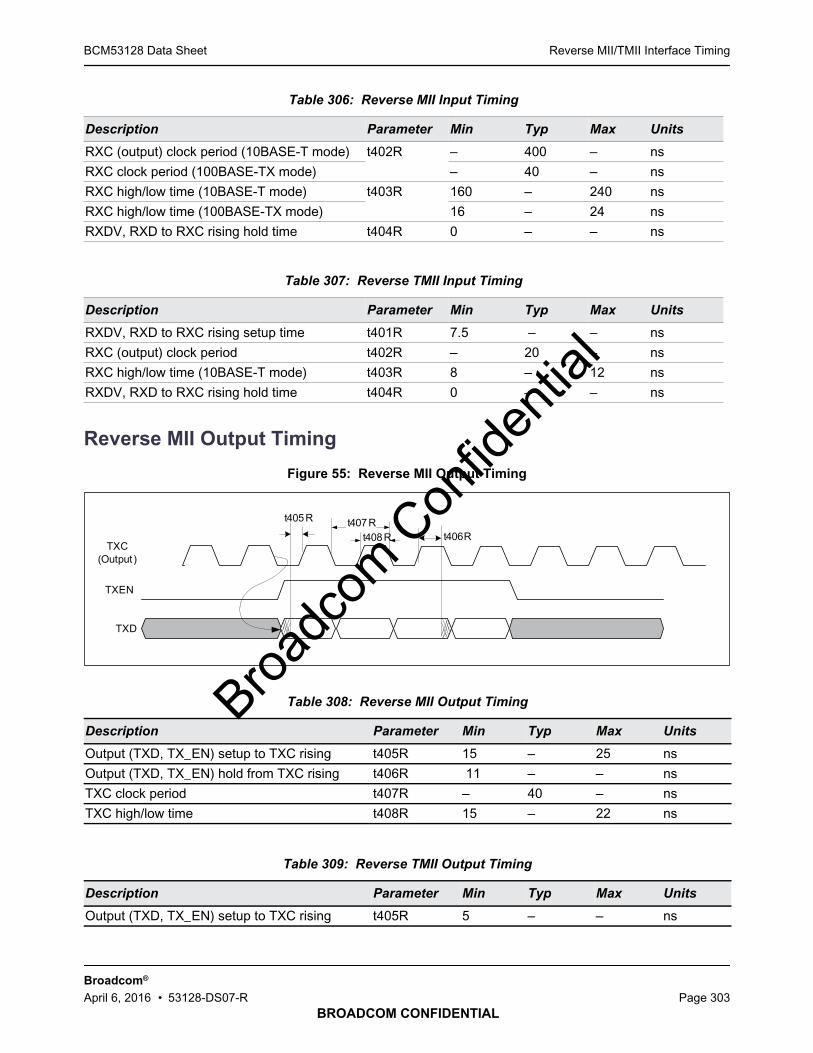
Reverse MII/TMII Interface TimingBCM53128 Data Sheet
BROADCOM CONFIDENTIAL
Broadcom®
April 6, 2016 • 53128-DS07-R Page 303
Reverse MII Output Timing
Figure 55: Reverse MII Output Timing
RXC (output) clock period (10BASE-T mode) t402R – 400 – ns
RXC clock period (100BASE-TX mode) – 40 – ns
RXC high/low time (10BASE-T mode) t403R 160 – 240 ns
RXC high/low time (100BASE-TX mode) 16 – 24 ns
RXDV, RXD to RXC rising hold time t404R 0 – – ns
Table 307: Reverse TMII Input Timing
Description Parameter Min Typ Max Units
RXDV, RXD to RXC rising setup time t401R 7.5 – – ns
RXC (output) clock period t402R – 20 – ns
RXC high/low time (10BASE-T mode) t403R 8 – 12 ns
RXDV, RXD to RXC rising hold time t404R 0 – – ns
Table 308: Reverse MII Output Timing
Description Parameter Min Typ Max Units
Output (TXD, TX_EN) setup to TXC rising t405R 15 – 25 ns
Output (TXD, TX_EN) hold from TXC rising t406R 11 – – ns
TXC clock period t407R – 40 – ns
TXC high/low time t408R 15 – 22 ns
Table 309: Reverse TMII Output Timing
Description Parameter Min Typ Max Units
Output (TXD, TX_EN) setup to TXC rising t405R 5 – – ns
Table 306: Reverse MII Input Timing
Description Parameter Min Typ Max Units
TXC(Output)
TXEN
TXD
t405R
t406Rt408Rt407R
Broadc
om C
onfid
entia
l

RGMII Interface TimingBCM53128 Data Sheet
BROADCOM CONFIDENTIAL
Broadcom®
April 6, 2016 • 53128-DS07-R Page 304
RGMII Interface Timing
The following specifies timing information regarding the IMP interface pins when configured in RGMII mode.
RGMII Output Timing (Normal Mode)
Figure 56: RGMII Output Timing (Normal Mode)
Output (TXD, TX_EN) hold from TXC rising t406R 5 – – ns
TXC clock period t407R – 20 – ns
TXC high/low time t408R 7.5 – 11 ns
Table 310: RGMII Output Timing (Normal Mode)
Description Parameter Min Typ Max Units
GTX_CLK clock period (1000M mode) – 7.2 8 8.8 ns
GTX_CLK clock period (100M mode) – 36 40 44 ns
GTX_CLK clock period (10M mode) – 360 400 440 ns
TskewT: data to clock output skew t201 –500 (1000M) 0 +500 (1000M) ps
Duty cycle for 1000M (GE) – 45 50 55 %
Duty cycle for 10/100M (FE) – 40 50 60 %
Note: The output timing in 10/100M operation is always as specified in the delayed mode.
Table 309: Reverse TMII Output Timing
Description Parameter Min Typ Max Units
GTX_CLK(at source)
TX_CTL
t201
TXD[3:0]
t201
Broadc
om C
onfid
entia
l
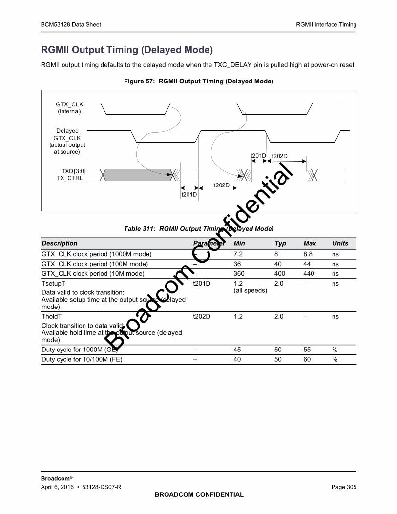
RGMII Interface TimingBCM53128 Data Sheet
BROADCOM CONFIDENTIAL
Broadcom®
April 6, 2016 • 53128-DS07-R Page 305
RGMII Output Timing (Delayed Mode)
RGMII output timing defaults to the delayed mode when the TXC_DELAY pin is pulled high at power-on reset.
Figure 57: RGMII Output Timing (Delayed Mode)
Table 311: RGMII Output Timing (Delayed Mode)
Description Parameter Min Typ Max Units
GTX_CLK clock period (1000M mode) – 7.2 8 8.8 ns
GTX_CLK clock period (100M mode) – 36 40 44 ns
GTX_CLK clock period (10M mode) – 360 400 440 ns
TsetupTData valid to clock transition:Available setup time at the output source (delayedmode)
t201D 1.2(all speeds)
2.0 – ns
TholdTClock transition to data valid:Available hold time at the output source (delayedmode)
t202D 1.2 2.0 – ns
Duty cycle for 1000M (GE) – 45 50 55 %
Duty cycle for 10/100M (FE) – 40 50 60 %
Delayed GTX_CLK
(actual output at source)
TX_CTRL
t201D
TXD[3:0]
t201D
t202D
t202D
GTX_CLK(internal)
Broadc
om C
onfid
entia
l
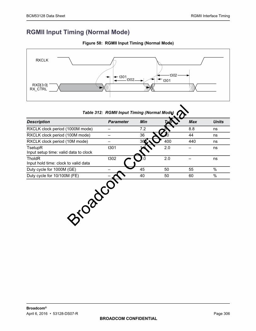
RGMII Interface TimingBCM53128 Data Sheet
BROADCOM CONFIDENTIAL
Broadcom®
April 6, 2016 • 53128-DS07-R Page 306
RGMII Input Timing (Normal Mode)
Figure 58: RGMII Input Timing (Normal Mode)
Table 312: RGMII Input Timing (Normal Mode)
Description Parameter Min Typ Max Units
RXCLK clock period (1000M mode) – 7.2 8 8.8 ns
RXCLK clock period (100M mode) – 36 40 44 ns
RXCLK clock period (10M mode) – 360 400 440 ns
TsetupRInput setup time: valid data to clock
t301 1.0 2.0 – ns
TholdRInput hold time: clock to valid data
t302 1.0 2.0 – ns
Duty cycle for 1000M (GE) – 45 50 55 %
Duty cycle for 10/100M (FE) – 40 50 60 %
RX_CTRLRXD[3:0]
RXCLK
t302 t301t302t301
Broadc
om C
onfid
entia
l
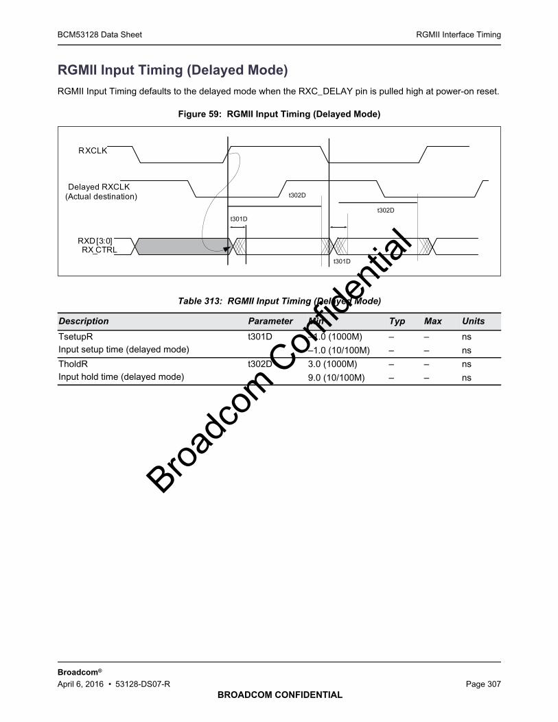
RGMII Interface TimingBCM53128 Data Sheet
BROADCOM CONFIDENTIAL
Broadcom®
April 6, 2016 • 53128-DS07-R Page 307
RGMII Input Timing (Delayed Mode)
RGMII Input Timing defaults to the delayed mode when the RXC_DELAY pin is pulled high at power-on reset.
Figure 59: RGMII Input Timing (Delayed Mode)
Table 313: RGMII Input Timing (Delayed Mode)
Description Parameter Min Typ Max Units
TsetupRInput setup time (delayed mode)
t301D –1.0 (1000M) – – ns
–1.0 (10/100M) – – ns
TholdRInput hold time (delayed mode)
t302D 3.0 (1000M) – – ns
9.0 (10/100M) – – ns
RXCLK
RX_CTRLRXD[3:0]
Delayed RXCLK(Actual destination)
t301D
t302D
t301D
t302D
Broadc
om C
onfid
entia
l
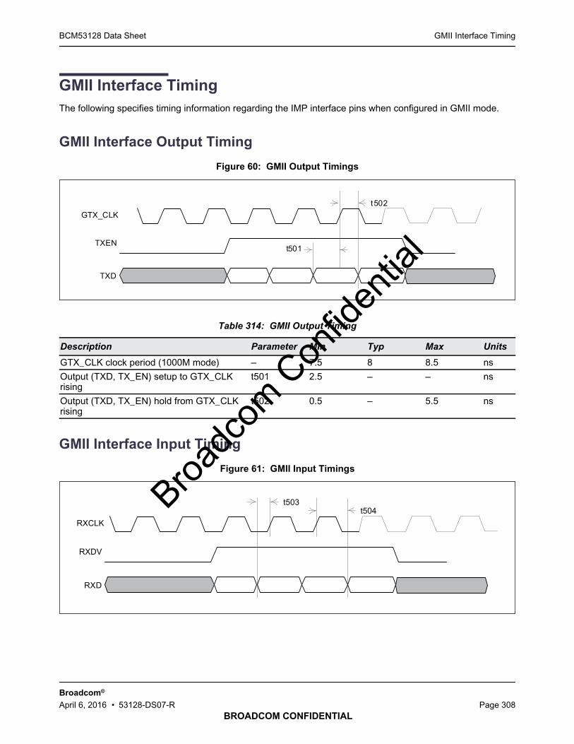
GMII Interface TimingBCM53128 Data Sheet
BROADCOM CONFIDENTIAL
Broadcom®
April 6, 2016 • 53128-DS07-R Page 308
GMII Interface Timing
The following specifies timing information regarding the IMP interface pins when configured in GMII mode.
GMII Interface Output Timing
Figure 60: GMII Output Timings
GMII Interface Input Timing
Figure 61: GMII Input Timings
Table 314: GMII Output Timing
Description Parameter Min Typ Max Units
GTX_CLK clock period (1000M mode) – 7.5 8 8.5 ns
Output (TXD, TX_EN) setup to GTX_CLKrising
t501 2.5 – – ns
Output (TXD, TX_EN) hold from GTX_CLKrising
t502 0.5 – 5.5 ns
TXEN
TXD
GTX_CLKt502
t501
RXDV
RXD
RXCLK
t503t504Broa
dcom
Con
fiden
tial

MDC/MDIO TimingBCM53128 Data Sheet
BROADCOM CONFIDENTIAL
Broadcom®
April 6, 2016 • 53128-DS07-R Page 309
MDC/MDIO Timing
The following specifies timing information regarding the MDC/MDIO interface pins.
Figure 62: MDC/MDIO Timing (Slave Mode)
Table 315: GMII Input Timing
Description Parameter Min Typ Max Units
RXCLK clock period (1000M mode) – – 8 – ns
(RXD, RX_DV) Setup to RX_CLK rising t503 2.0 – – ns
(RXD, RX_DV) Hold from RX_CLKrising
t504 0.0 – – ns
Table 316: MDC/MDIO Timing (Slave Mode)
Description Parameter Minimum Typical Maximum Unit
MDC cycle time t401 80 – – ns
MDC high/low – 30 – – ns
MDC rise/fall time t402 – – 10 ns
MDIO input setup time to MDC rising t403 7.5 – – ns
MDIO input hold time from MDC rising t404 7.5 – – ns
MDIO output delay from MDC rising t405 0 – 45 ns
Table 317: MDC/MDIO Timing (Master Mode)
Description Parameter Minimum Typical Maximum Unit
MDC cycle time t401 400 – – ns
MDC high/low – 160 – 240 ns
MDIO(Into PHY)
MDC
MDIO(From PHY)
t405
t403
t401
t404
t402
t402
Broadc
om C
onfid
entia
l
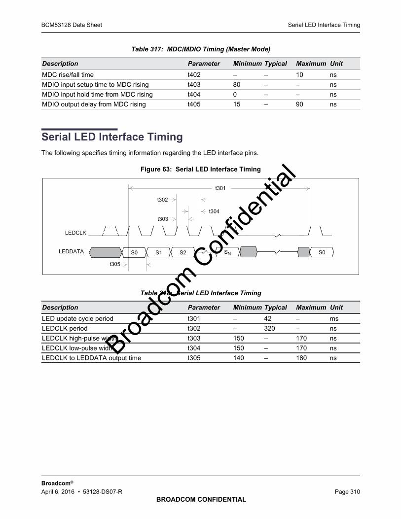
Serial LED Interface TimingBCM53128 Data Sheet
BROADCOM CONFIDENTIAL
Broadcom®
April 6, 2016 • 53128-DS07-R Page 310
Serial LED Interface Timing
The following specifies timing information regarding the LED interface pins.
Figure 63: Serial LED Interface Timing
MDC rise/fall time t402 – – 10 ns
MDIO input setup time to MDC rising t403 80 – – ns
MDIO input hold time from MDC rising t404 0 – – ns
MDIO output delay from MDC rising t405 15 – 90 ns
Table 318: Serial LED Interface Timing
Description Parameter Minimum Typical Maximum Unit
LED update cycle period t301 – 42 – ms
LEDCLK period t302 – 320 – ns
LEDCLK high-pulse width t303 150 – 170 ns
LEDCLK low-pulse width t304 150 – 170 ns
LEDCLK to LEDDATA output time t305 140 – 180 ns
Table 317: MDC/MDIO Timing (Master Mode)
Description Parameter Minimum Typical Maximum Unit
LEDDATA
LEDCLK
t301
S0 S1 S2 S S0N
t305
t302
t303t304
Broadc
om C
onfid
entia
l
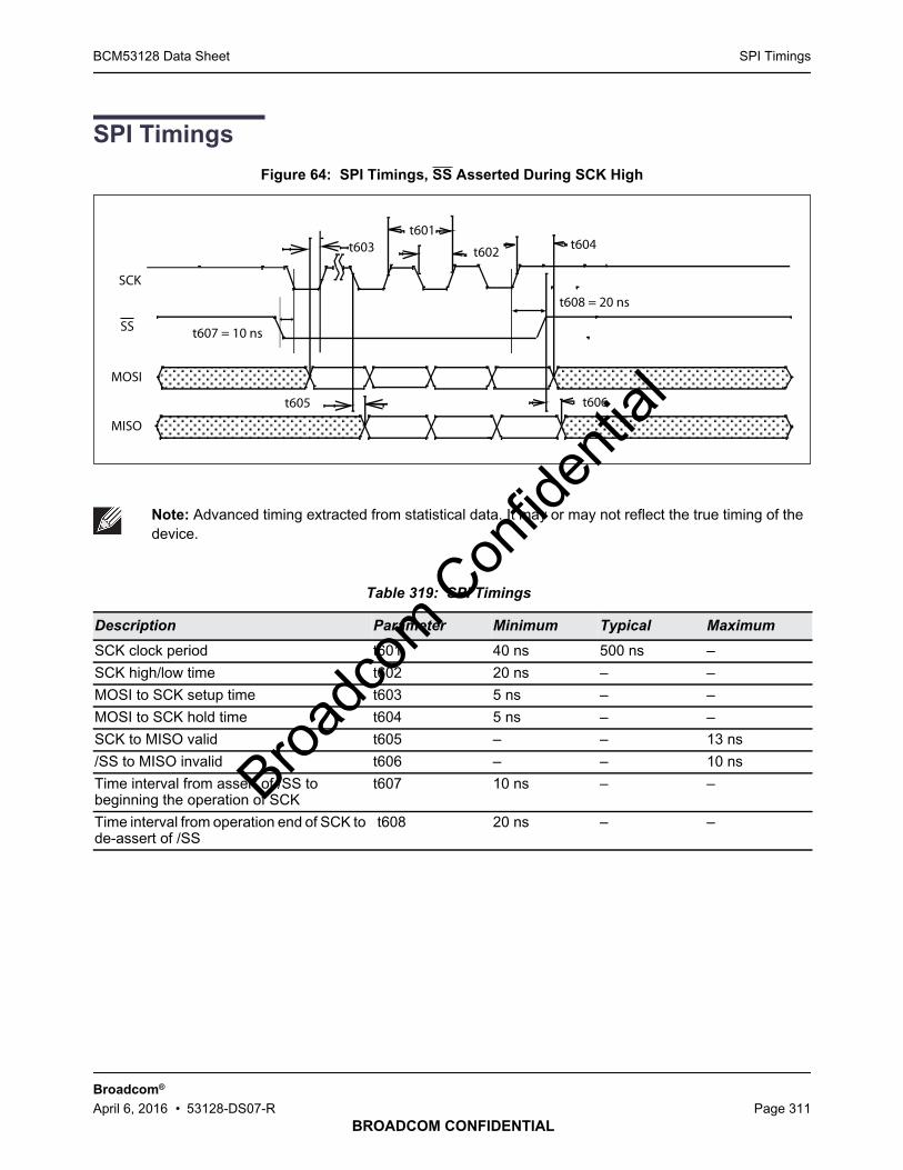
SPI TimingsBCM53128 Data Sheet
BROADCOM CONFIDENTIAL
Broadcom®
April 6, 2016 • 53128-DS07-R Page 311
SPI Timings
Figure 64: SPI Timings, SS Asserted During SCK High
Note: Advanced timing extracted from statistical data. It may or may not reflect the true timing of thedevice.
Table 319: SPI Timings
Description Parameter Minimum Typical Maximum
SCK clock period t601 40 ns 500 ns –
SCK high/low time t602 20 ns – –
MOSI to SCK setup time t603 5 ns – –
MOSI to SCK hold time t604 5 ns – –
SCK to MISO valid t605 – – 13 ns
/SS to MISO invalid t606 – – 10 ns
Time interval from assert of /SS tobeginning the operation of SCK
t607 10 ns – –
Time interval from operation end of SCK tode-assert of /SS
t608 20 ns – –
SCK
SS
MOSI
MISO
t605 t606
t603t601
t602 t604
t607 = 10 ns
t608 = 20 ns
Broadc
om C
onfid
entia
l

EEPROM TimingBCM53128 Data Sheet
BROADCOM CONFIDENTIAL
Broadcom®
April 6, 2016 • 53128-DS07-R Page 312
EEPROM Timing
Figure 65: EEPROM Timing
Table 320: EEPROM Timing
Description Parameter Minimum Typical Maximum
SCK clock frequency t701 – 200 kHz –
SCK high/low time t702 – 2.5 s –
MISO to SCK rising setup time t703 50 ns – –
MISO to SCK rising hold time t704 10 ns – –
SCK low to SS, MOSI valid time t705 30 ns – 100 ns
SCK low to SS, MOSI invalid time t706 30 ns – –
SCK
SS
MISO
t705
MOSI
t701
t702
t703 t704
t706
Broadc
om C
onfid
entia
l

Serial Flash TimingBCM53128 Data Sheet
BROADCOM CONFIDENTIAL
Broadcom®
April 6, 2016 • 53128-DS07-R Page 313
Serial Flash Timing
Figure 66: Serial Flash Timing
Table 321: Serial Flash Timing
Description Parameter Minimum Typical Maximum
FSCLK clock frequency t801 – 22.72 MHz 50 MHz
FSI to FSCLK rising setup time t802 10 ns – –
FSI to FSCLK rising hold time t803 0 ns – –
FSCLK to FSO delay t804 5 ns – FSCLK cycletime - 5 ns
The falling edge of FCSB to first rising edgeof FSCLK
t805 5 ns – –
The last rising edge of FSCLK to rising edgeof FCSB
t806 5 ns – –
Broadc
om C
onfid
entia
l

Thermal CharacteristicsBCM53128 Data Sheet
BROADCOM CONFIDENTIAL
Broadcom®
April 6, 2016 • 53128-DS07-R Page 314
Section 10: Thermal Characteristics
Note: The maximum allowed junction temperature is 125 ºC. Table 322 and Table 323 on page 314show the estimated junction temperature with heat sink.
Table 322: BCM53128KQLE Package without Heat Sink, 4-Layer Board, P = 3.1W
Device power dissipation, P (W) 3.1
Ambient air temperature Ta (ºC) 70
JA is still air (ºC/W) 17.48
JB (ºC/W) 0.98
JC (ºC/W) 14.12
Package Thermal Performance Data
Air Velocity TJ_max TT JA JT JB
m/s ft/min (ºC) (ºC) (ºC/W) (ºC/W) (ºC/W)
0 0 124.19 122.86 17.48 0.43 9.35
0.508 100 118.59 117.26 15.67 0.43 9.38
1.016 200 115.70 114.25 14.74 0.47 9.44
2.032 400 112.74 111.07 13.79 0.54 9.46
3.048 600 111.10 109.01 13.26 0.68 9.40
Table 323: BCM53128KQLE Package with Heat Sink, 2-Layer Board, P = 3.1W
Device power dissipation, P (W) 3.1
Ambient air temperature Ta (ºC) 70
JA is still air (ºC/W) 16.22
JB (ºC/W) 0.98
JC (ºC/W) 14.12
External heat sink Heat sink: 28 mm x 28 mm x 15 mm, k = 180 (W/m*k), aluminium blade-fin.Thermal interface: Loctite 384, 0.1 mm thick, k = 0.757 W/m-k
Package Thermal Performance Data
Air Velocity TJ_max TT JA JT JB
m/s ft/min (ºC) (ºC) (ºC/W) (ºC/W) (ºC/W)
0 0 120.29 96.93 16.22 7.53 10.10
0.508 100 112.94 88.80 13.85 7.79 9.89
1.016 200 111.07 86.80 13.25 7.83 9.85
2.032 400 109.30 85.00 12.68 7.84 9.85
Broadc
om C
onfid
entia
l

Thermal CharacteristicsBCM53128 Data Sheet
BROADCOM CONFIDENTIAL
Broadcom®
April 6, 2016 • 53128-DS07-R Page 315
3.048 600 108.40 84.00 12.39 7.87 9.82
Table 324: BCM53128IQLE Package with Heat Sink, 4-layer Board, P=3.1W
Device power dissipation, P (W) 3.1
Ambient air temperature Ta (ºC) 85
JA is still air (ºC/W) 12.60
JB (ºC/W) 0.98
JC (ºC/W) 14.12
External heat sink Heat sink: 28 mm x 28 mm x 15 mm, k = 180 (W/m*k), aluminium blade-fin.Thermal interface: Loctite 384, 0.1 mm thick, k = 0.757 W/m-k
Package Thermal Performance Data
Air Velocity TJ_max TT JA JT JB
m/s ft/min (ºC) (ºC) (ºC/W) (ºC/W) (ºC/W)
0 0 124.07 106.76 12.6 5.58 7.16
0.508 100 118.36 100.33 10.76 5.81 7.03
1.016 200 116.69 98.55 10.22 5.85 7.03
2.032 400 114.97 96.84 9.67 5.85 7.03
3.048 600 114.25 96.12 9.43 5.85 7.02
Table 323: BCM53128KQLE Package with Heat Sink, 2-Layer Board, P = 3.1W
Broadc
om C
onfid
entia
l
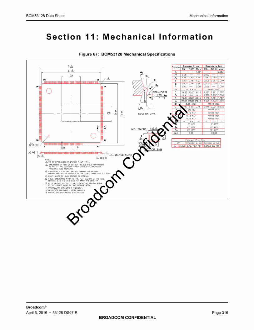
Mechanical InformationBCM53128 Data Sheet
BROADCOM CONFIDENTIAL
Broadcom®
April 6, 2016 • 53128-DS07-R Page 316
Section 11: Mechanical Information
Figure 67: BCM53128 Mechanical Specifications
Broadc
om C
onfid
entia
l
Ordering InformationBCM53128 Data Sheet
BROADCOM CONFIDENTIAL
Broadcom®
April 6, 2016 • 53128-DS07-R Page 317
Section 12: Ordering Information
Table 325: Ordering Information
Part Number Package Ambient Temperature
BCM53128KQLE(G) 256 eLQFP 0°C to 70°C
BCM53128IQLE(G) 256 eLQFP –45°C to 85°C
Note: (G) represents the lead-free package option.
Broadc
om C
onfid
entia
l

Broadcom
Web: www.broadcom.comCorporate Headquarters: San Jose, CA© 2016 by Broadcom. All rights reserved.
53128-DS07-R April 6, 2016
Broadcom® reserves the right to make changes without further notice to any products or data herein to improve reliability,function, or design.
Information furnished by Broadcom is believed to be accurate and reliable. However, Broadcom does not assume any liabilityarising out of the application or use of this information, nor the application or use of any product or circuit described herein,neither does it convey any license under its patent rights nor the rights of others.
BCM53128 Data Sheet
Broadc
om C
onfid
entia
l

Mouser Electronics
Authorized Distributor
Click to View Pricing, Inventory, Delivery & Lifecycle Information: Broadcom Limited:
BCM53128IQLEG BCM53128KQLEG