battery monitor ic with alarm output for gas gauge applications · ideal for implementation of...
TRANSCRIPT

September 2011 Doc ID 022198 Rev 1 1/23
23
STC3105
Battery monitor IC with alarm output for gas gauge applications
Features 0.5% accuracy battery voltage monitoring
Low battery alarm output with programmable thresholds
Low power: 60 µA in power-saving mode, 2 µA max in standby mode
Ideal for implementation of robust gas gauge systems using open-circuit voltage and coulomb counter methods
Small 3x2 mm package
Applications Mobile phones, multimedia players, digital
cameras
Portable medical equipment
DescriptionThe STC3105 battery monitor includes the hardware functions required to implement a low-cost gas gauge for battery monitoring. The STC3105 uses accurate measurements of the battery voltage to estimate a battery’s state-of-charge (SOC). It uses a low cost sense resistor to precisely sense the charge or discharge states, detect light-load conditions without ambiguity for voltage measurements, and accurate SOC calculation. The coulomb counter method is used for SOC tracking in high-load conditions.
An alarm output signals a low SOC condition, and can also indicate low battery voltage. The alarm threshold levels are programmable.
The device is programmable through an I2C interface.
TDFN8 3x2(Plastic micropackage)
12
3
4 5
6
7
8ALM
SCLGND CG
VINSDA VCC
NC
Pin connections(top view)
www.st.com

Contents STC3105
2/23 Doc ID 022198 Rev 1
Contents
1 Block diagram . . . . . . . . . . . . . . . . . . . . . . . . . . . . . . . . . . . . . . . . . . . . . . 3
2 Pin assignment . . . . . . . . . . . . . . . . . . . . . . . . . . . . . . . . . . . . . . . . . . . . . 4
3 Absolute maximum ratings and operating conditions . . . . . . . . . . . . . 5
4 Electrical characteristics . . . . . . . . . . . . . . . . . . . . . . . . . . . . . . . . . . . . . 6
5 Application information . . . . . . . . . . . . . . . . . . . . . . . . . . . . . . . . . . . . . . 9
6 Functional description . . . . . . . . . . . . . . . . . . . . . . . . . . . . . . . . . . . . . . 10
6.1 Battery monitoring functions and operating modes . . . . . . . . . . . . . . . . . 10
6.2 Battery voltage monitoring . . . . . . . . . . . . . . . . . . . . . . . . . . . . . . . . . . . . 10
6.3 Current sensing . . . . . . . . . . . . . . . . . . . . . . . . . . . . . . . . . . . . . . . . . . . . 10
6.4 Coulomb counter . . . . . . . . . . . . . . . . . . . . . . . . . . . . . . . . . . . . . . . . . . . 11
6.5 Alarm output . . . . . . . . . . . . . . . . . . . . . . . . . . . . . . . . . . . . . . . . . . . . . . . 11
6.6 Battery voltage relaxation timer . . . . . . . . . . . . . . . . . . . . . . . . . . . . . . . . 12
6.7 Timing diagram in run mode . . . . . . . . . . . . . . . . . . . . . . . . . . . . . . . . . . . 13
7 I2C interface . . . . . . . . . . . . . . . . . . . . . . . . . . . . . . . . . . . . . . . . . . . . . . . 14
7.1 Read and write operations . . . . . . . . . . . . . . . . . . . . . . . . . . . . . . . . . . . . 14
7.2 Register map . . . . . . . . . . . . . . . . . . . . . . . . . . . . . . . . . . . . . . . . . . . . . . 16
8 Package information . . . . . . . . . . . . . . . . . . . . . . . . . . . . . . . . . . . . . . . . 18
8.1 TDFN8 package information . . . . . . . . . . . . . . . . . . . . . . . . . . . . . . . . . . 19
9 Ordering information . . . . . . . . . . . . . . . . . . . . . . . . . . . . . . . . . . . . . . . 21
10 Revision history . . . . . . . . . . . . . . . . . . . . . . . . . . . . . . . . . . . . . . . . . . . 22

STC3105 Block diagram
Doc ID 022198 Rev 1 3/23
1 Block diagram
Figure 1. STC3105 internal block diagram

Pin assignment STC3105
4/23 Doc ID 022198 Rev 1
2 Pin assignment
Note: I: inputO: outputOD: open drainA: analogD: digital
Table 1. STC3105 pin description
Pin Pin name Type Function
1 ALM I/ODAlarm signal output, open drain, external pull-up resistor is required
2 SDA I/OD I2C serial data
3 SCL I_D I2C serial clock
4 GND Ground Analog and digital ground
5 CG I_A Current sensing input
6 NC Reserved test pin. Do not connect.
7 VCC Supply Power supply
8 VIN I_A Battery voltage sensing input

STC3105 Absolute maximum ratings and operating conditions
Doc ID 022198 Rev 1 5/23
3 Absolute maximum ratings and operating conditions
Table 2. Absolute maximum ratings
Symbol Parameter Value Unit
VCCMAX Maximum voltage on VCC pin 7 V
VIO Voltage on I/O pins -0.3 to 7 V
TSTG Storage temperature -55 to 150 ° C
TJ Maximum junction temperature 150 ° C
ESD Electrostatic discharge (HBM: human body model) 2 kV
Table 3. Operating conditions
Symbol Parameter Value Unit
VCC Operating supply voltage on VCC 2.7 to 5.5 V
VMIN Minimum voltage on VCC for RAM content retention 2.0 V
TOPER Operating free air temperature range -40 to 85 ° C

Electrical characteristics STC3105
6/23 Doc ID 022198 Rev 1
4 Electrical characteristics
Table 4. Electrical characteristics (2.7 V < VCC < 4.5 V, -20 ° C to 70 ° C)
Symbol Parameter Conditions Min Typ Max Units
Supply
ICC Operating current consumptionAverage value over 4 s in:– power-saving mode
– Active mode
60
-
70
100
µA
µA
ISTBY Current consumption in standby Standby mode, inputs=0V 2 µA
IPDN Current consumption in power-down VCC < UVLOTH, inputs=0V 1 µA
UVLOTH Undervoltage threshold (VCC decreasing) 2.5 2.6 2.7 V
UVLOHYST Undervoltage threshold hysteresis 100 mV
POR Power-on reset threshold (VCC decreasing) 2.0 V
Current sensing
Vin_gg Input voltage range -80 +80 mV
IIN Input current for CG pin 500 nA
ADC_res AD converter granularity 11.77 µV
ADC_offset AD converter offset CG = 0 V -3 3 LSB
ADC_time AD conversion time 500 ms
ADC_accAD converter gain accuracy at full scale(using external sense resistor)
25 ° COver temperature range
0.5-
-1
%%
FOSC Internal time base frequency 32768 Hz
Osc_acc Internal time base accuracy25 ° C, VCC = 3.6 Vover temperature and voltage ranges
2
2.5
%
%
Cur_res Current register LSB value 11.77 µV
Chg_res Charge register LSB value =Cur_res*2^12*0.5/3600 6.70 µVh

STC3105 Electrical characteristics
Doc ID 022198 Rev 1 7/23
Battery voltage measurement
Vin_adc Input voltage range 0 5 V
LSB LSB value 2.44 mV
ADC_time AD conversion time 250 ms
Volt_acc Battery voltage measurement accuracy 2.7 V<Vin<4.5 V, VCC=Vin -0.5 +0.5 %
Digital I/O pins (SCL, SDA, ALM)
Vih Input logic high 1.2 V
Vil Input logic low 0.35 V
Vol Output logic low (SDA, ALM) Iol = 4 mA 0.4 V
Table 4. Electrical characteristics (2.7 V < VCC < 4.5 V, -20 ° C to 70 ° C) (continued)
Symbol Parameter Conditions Min Typ Max Units

Electrical characteristics STC3105
8/23 Doc ID 022198 Rev 1
Figure 2. I2C timing diagram
Table 5. I2C timing - VIO= 2.8 V, Tamb = -20 °C to 70 ° C (unless otherwise specified)
Symbol Parameter Conditions Min Typ Max Unit
Fscl SCL clock frequency
-
0
-
400 kHz
thd,sta Hold time (repeated) START condition 0.6 µs
tlow LOW period of the SCL clock 1.3 µs
thigh HIGH period of the SCL clock 0.6 µs
tsu,dat Setup time for repeated START condition 0.6 µs
thd,dat Data hold time 0 0.9 µs
tsu,dat Data setup time 100 ns
tr Rise time of both SDA and SCL signals20+
0.1Cb300 ns
tf Fall time of both SDA and SCL signals20+
0.1Cb300 ns
tsu,sto Setup time for STOP condition 0.6 µs
tbufBus free time between a STOP and
START condition1.3 µs
Cb Capacitive load for each bus line 400 pF

STC3105 Application information
Doc ID 022198 Rev 1 9/23
5 Application information
Figure 3. Example of an application schematic using the STC3105
Table 6. External component list
Name Value Tolerance Comments
Rcg 10 to 50 mΩ 2% to 5% Current sense resistor
C1 1 µF Supply decoupling capacitor
C2 220 nF Battery voltage input filter (optional)
R1 1 kΩ Battery voltage input filter (optional)

Functional description STC3105
10/23 Doc ID 022198 Rev 1
6 Functional description
6.1 Battery monitoring functions and operating modesThe monitoring functions include the measurement of the battery voltage and battery current. A coulomb counter is used to track the state-of-charge when the battery is charging or is discharging at a high rate. A 14-bit sigma-delta A/D converter is used to measure both the voltage and current.
The STC3105 can operate in two modes with different power consumption. The selection is made by the PWR_SAVE bit in the register 0 (Refer to Table 11 on page 17 for register 0 definition).
In power-saving mode, the current is measured only half of the time. This saves about half of the power consumption.
In active mode, the current is continuously measured (except for one conversion cycle used every 4 seconds for the voltage measurement). This provides the highest accuracy from the coulomb counter.
When the battery voltage falls below the undervoltage lockout threshold of 2.7 V, the monitoring functions are stopped and the STC3105 stays in power-down mode with minimum quiescent current. All registers are maintained down to 2.0 V. Below 2.0 V, the registers are reset to their default power-on values.
By writing 0 to the GG_RUN bit in register 0, the STC3105 measurement is automatically stopped and the register values are frozen and unchanged. After the GG_RUN bit is again set to 1, the STC3105 continues to measure from the point it was stopped.
6.2 Battery voltage monitoringThe battery voltage is measured by using one conversion cycle of the A/D converter every 4 seconds.
The conversion cycle takes 213 = 8192 clock cycles. Using the 32768 Hz internal clock, the conversion cycle time is 250 ms.
The voltage range is 0 to 5 V, and the resolution is 2.44 mV. The accuracy of the voltage measurement is ±0.5% over the temperature range. This allows accurate state-of-charge information from the battery open-circuit voltage.
6.3 Current sensingThe voltage drop across the sense resistor is integrated during a conversion period and input to the 14-bit sigma-delta A/D converter.
Using the 32768 Hz internal clock, the conversion cycle time is 500 ms for a 14-bit resolution. The LSB value is 11.77 µV. The A/D converter output is in two’s complement format.
When a conversion cycle is completed, the result is added to the coulomb counter accumulator and the number of conversions is incremented in a 16-bit counter.
STC3105 Functional description
Doc ID 022198 Rev 1 11/23
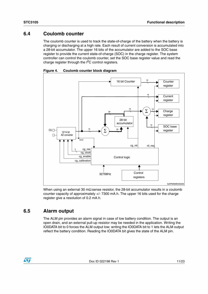
6.4 Coulomb counterThe coulomb counter is used to track the state-of-charge of the battery when the battery is charging or discharging at a high rate. Each result of current conversion is accumulated into a 28-bit accumulator. The upper 16 bits of the accumulator are added to the SOC base register to provide the current state-of-charge (SOC) in the charge register. The system controller can control the coulomb counter, set the SOC base register value and read the charge register through the I2C control registers.
Figure 4. Coulomb counter block diagram
When using an external 30 mΩ sense resistor, the 28-bit accumulator results in a coulomb counter capacity of approximately +/- 7300 mA.h. The upper 16 bits used for the charge register give a resolution of 0.2 mA.h.
6.5 Alarm outputThe ALM pin provides an alarm signal in case of low battery condition. The output is an open drain, and an external pull-up resistor may be needed in the application. Writing the IO0DATA bit to 0 forces the ALM output low; writing the IO0DATA bit to 1 lets the ALM output reflect the battery condition. Reading the IO0DATA bit gives the state of the ALM pin.

Functional description STC3105
12/23 Doc ID 022198 Rev 1
When the IO0DATA bit is 1 and the alarm function is enabled by the ALM_ENA bit, the ALM pin is driven low if either of these two conditions is met:
battery state-of-charge (SOC) less than the programmed threshold
battery voltage less than the programmed low voltage level
When a low-voltage or low-SOC condition is triggered, the STC3105 drives the ALM pin low and sets the ALM_VOLT or ALM_SOC bit in REG_CTRL.
The ALM pin remains low (even if the conditions disappear) until the software writes the ALM_VOLT and ALM_SOC bits to 0 to clear the interrupt.
Clearing the ALM_VOLT or ALM_SOC while the corresponding low-voltage or low-SOC condition is still true does not generate another interrupt; this condition must disappear first and must be detected again before another interrupt (ALM pin driven low) is generated for this alarm. The other alarm condition, if not yet triggered, can still generate an interrupt.
Usually, the low-SOC alarm occurs first to warn the application of a low battery condition, then if no action is taken and the battery discharges further, the low-voltage alarm signals a nearly-empty battery condition.
At power-up, or when the STC3105 is reset, the alarm output is disabled (ALM_ENA bit = 0), the threshold levels (low-voltage alarm, low-SOC alarm) are cleared, and the base SOC and relaxation counter are cleared.
6.6 Battery voltage relaxation timerA battery relaxation timer is counted from the time that the current is below 0 and above the current threshold, meaning the battery is in a light-load condition. The relaxation counter register is an 8-bit read-only register clocked every 2 voltage conversion (8 s) and can go up to about 30 min; when the counter reaches its max value 0xff, it stops at this max value. The counter is cleared when the current is above 0 (charging) or below the current threshold (high rate discharge).
The relaxation counter register is read from I2C by the gas gauge firmware to check that the battery voltage had enough time to relax from the last time the current was high or charging.
The current threshold register is an 8-bit R/W register set by the gas gauge firmware from I2C. It can be programmed from 0.1 to 100% of the full scale current range with 0.4% steps
Figure 5. Battery voltage relaxation counter

STC3105 Functional description
Doc ID 022198 Rev 1 13/23
6.7 Timing diagram in run modeFigures 6 and 7 describe the timing diagrams of the STC3105. It is assumed that the gas gauge has been reset with GG_RST before GG_RUN=1.
Figure 6. Timing diagram in active run mode
Figure 7. Timing diagram in power-saving run mode
The voltage is measured first after GG_RUN bit is set to 1. The charge accumulator is updated every 500 ms using the last current value. The measurement cycles can be interrupted by setting GG_RUN=0 and the current conversion cycle is aborted.

I2C interface STC3105
14/23 Doc ID 022198 Rev 1
7 I2C interface
7.1 Read and write operationsThe interface is used to control and read the current accumulator and registers. It is compatible with the Philips I2C registered trademark (version 2.1). It is a slave serial interface with a serial data line (SDA) and a serial clock line (SCL).
SCL: input clock used to shift data
SDA: input/output bidirectional data transfers
A filter rejects the potential spikes on the bus data line to preserve data integrity.
The bidirectional data line supports transfers up to 400 kbit/s (fast mode). The data is shifted to and from the chip on the SDA line, MSB first.
The first bit must be high (START) followed by the 7-bit device address and the read/write control bit. Bits DevADDR0 to DevADDR2 are factory-programmable, the default device address value being 1110 000 (AddrID0 = AddrID1 = AddrID2 = 0). The STC3105 then sends an acknowledge at the end of an 8-bit long sequence. The next 8 bits correspond to the register address followed by another acknowledge.
The data field is the last 8-bit long sequence sent, followed by a last acknowledge.
Table 7. Device address format
b7 b6 b5 b4 b3 b2 b1 b0
1 1 1 0 DevADDR2 DevADDR1 DevADDR0 R/W
Table 8. Register address format
b7 b6 b5 b4 b3 b2 b1 b0
RegADDR7 RegADDR6 RegADDR5 RegADDR4 RegADDR3 RegADDR2 RegADDR1 RegADDR0
Table 9. Register data format
b7 b6 b5 b4 b3 b2 b1 b0
DATA7 DATA6 DATA5 DATA4 DATA3 DATA2 DATA1 DATA0

STC3105 I2C interface
Doc ID 022198 Rev 1 15/23
Figure 8. Read operation
Figure 9. Write operation

I2C interface STC3105
16/23 Doc ID 022198 Rev 1
7.2 Register mapThe register space provides 17 control registers, 1 read-only register for device ID and 16 read/write RAM working registers reserved for the gas gauge algorithm. Mapping of all registers is shown in Table 10. Detailed descriptions of registers 0 (REG_MODE) and 1 (REG_CTRL) are shown in Table 11 and Table 12. All registers are reset to default values at power-on or reset, and the PORDET bit in register REG_CTRL is used to indicate the occurrence of a power-on reset.
Values held in consecutive registers (such as the charge value in the REG_CHARGE_LOW and REG_CHARGE_HIGH registers) must be read with a single I2C access to ensure data integrity. It is possible to read multiple values in one I2C access; all values will be consistent.
Table 10. Register map
NameAddress (decimal)
Type Description
Control registers 0 to 23
REG_MODE 0 R/W Mode register
REG_CTRL 1 R/W Control and status register
REG_CHARGE_LOW 2 R State-of-charge data, bits 0-7
REG_CHARGE_HIGH 3 R State-of-charge data, bits 8-15
REG_COUNTER_LOW 4 R Number of conversions, bits 0-7
REG_COUNTER_HIGH 5 R Number of conversions, bits 8-15
REG_CURRENT_LOW 6 R Battery current value, bits 0-7
REG_CURRENT_HIGH 7 R Battery current value, bits 8-15
REG_VOLTAGE_LOW 8 R Battery voltage value, bits 0-7
REG_VOLTAGE_HIGH 9 R Battery voltage value, bits 8-15
REG_SOC_BASE_LOW 10 R/W SOC base value, bits 0-7
REG_SOC_BASE_HIGH 11 R/W SOC base value, bits 8-15
REG_ALARM_SOC_LOW 12 R/W SOC alarm level, bits 0-7
REG_ALARM_SOC_HIGH 13 R/W SOC alarm level, bits 8-15
REG_ALARM_VOLTAGE 14 R/W Battery low voltage alarm level
REG_CURRENT_THRES 15 R/WCurrent threshold for the voltage relaxation counter
REG_RELAX_COUNT 16 R Voltage relaxation counter
Device ID register
REG_ID 24 R Part type ID = 12h
RAM registers 32 to 47
REG_RAM0 32 R/W Working register 0 for gas gauge
... ... ...
REG_RAM15 47 R/W Working register 15 for gas gauge

STC3105 I2C interface
Doc ID 022198 Rev 1 17/23
The charge data is coded in 2’s complement format, and the LSB value is 6.70 uV.h.The battery current is coded in 2’s complement format, and the LSB value is 11.77 uV.The battery voltage is coded in binary format, and the LSB value is 2.44 mV.
Table 11. REG_MODE - address 0
Name Pos. Type Def. Description
0 Unused
1 R/W 0 Reserved. Write this bit to 0.
PWR_SAVE 2 R/W 0 0: active mode, 1: power-saving mode
ALM_ENA 3 R/W 0 Alarm function: 0: disabled, 1: enabled
GG_RUN 4 R/W 0
0: standby mode. Accumulator and counter registers are frozen, gas gauge and battery monitor functions are in standby.1: operating mode.
[7..5] Unused
Table 12. REG_CTRL - address 1
Name Pos. Type Def. Description
IO0DATA 0
R XALM pin status:0 = ALM input is low, 1 = ALM input is high
W 1ALM pin output drive:0 = ALM is forced low, 1 = ALM is driven by the alarm conditions
GG_RST 1 W 00: no effect1: resets the charge accumulator and conversion counter. GG_RST is a self-clearing bit.
GG_EOC 2 R 0Set at the end of a battery current conversion cycle. Clears upon reading.
VM_EOC 3 R 0Set at the end of a battery voltage conversion cycle. Clears upon reading.
PORDET 4
R 1Power on reset (POR) detection bit:0 = no POR event occurred,1 = POR event occurred
W 0
Soft reset:0 = release the soft-reset and clear the POR detection bit, 1 = assert the soft-reset and set the POR detection bit.
ALM_SOC 5 R/W 0 Set by a low-SOC condition. Cleared by writing 0.
ALM_VOLT 6 R/W 0Set by a low-voltage condition. Cleared by writing 0.
7 Unused

Package information STC3105
18/23 Doc ID 022198 Rev 1
8 Package information
In order to meet environmental requirements, ST offers these devices in different grades of ECOPACK® packages, depending on their level of environmental compliance. ECOPACK® specifications, grade definitions and product status are available at: www.st.com. ECOPACK® is an ST trademark.

STC3105 Package information
Doc ID 022198 Rev 1 19/23
8.1 TDFN8 package information
Figure 10. TDFN8 3 x 2 x 0.75 mm package mechanical drawing (pitch 0.65 mm)
GAPMSMD00033

Package information STC3105
20/23 Doc ID 022198 Rev 1
Figure 11. Recommended land pattern
Table 13. TDFN8 3 x 2 x 0.75 mm package mechanical data (pitch 0.65 mm)
Ref.
Dimensions
Millimeters Inches
Min. Typ. Max. Min. Typ. Max.
A 0.70 0.75 0.80 0.028 0.030 0.031
A1 0.00 0.02 0.05 0.000 0.000 0.002
b 0.25 0.30 0.35 0.010 0.012 0.014
D 2.90 3.00 3.10 0.114 0.118 0.122
E 1.90 2.00 2.10 0.075 0.079 0.083
e 0.65 0.026
L 0.45 0.55 0.65 0.018 0.022 0.026
L1 0.55 0.65 0.75 0.022 0.026 0.030
GAPMSMD00034

STC3105 Ordering information
Doc ID 022198 Rev 1 21/23
9 Ordering information
Table 14. Order codes
Part numberTemperature
rangePackage Packing Marking
STC3105IQT -40°C, +85°C TDFN8 3 x 2 Tape and reel O203

Revision history STC3105
22/23 Doc ID 022198 Rev 1
10 Revision history
Table 15. Document revision history
Date Revision Changes
07-Sep-2011 1 First release.

STC3105
Doc ID 022198 Rev 1 23/23
Please Read Carefully:
Information in this document is provided solely in connection with ST products. STMicroelectronics NV and its subsidiaries (“ST”) reserve theright to make changes, corrections, modifications or improvements, to this document, and the products and services described herein at anytime, without notice.
All ST products are sold pursuant to ST’s terms and conditions of sale.
Purchasers are solely responsible for the choice, selection and use of the ST products and services described herein, and ST assumes noliability whatsoever relating to the choice, selection or use of the ST products and services described herein.
No license, express or implied, by estoppel or otherwise, to any intellectual property rights is granted under this document. If any part of thisdocument refers to any third party products or services it shall not be deemed a license grant by ST for the use of such third party productsor services, or any intellectual property contained therein or considered as a warranty covering the use in any manner whatsoever of suchthird party products or services or any intellectual property contained therein.
UNLESS OTHERWISE SET FORTH IN ST’S TERMS AND CONDITIONS OF SALE ST DISCLAIMS ANY EXPRESS OR IMPLIEDWARRANTY WITH RESPECT TO THE USE AND/OR SALE OF ST PRODUCTS INCLUDING WITHOUT LIMITATION IMPLIEDWARRANTIES OF MERCHANTABILITY, FITNESS FOR A PARTICULAR PURPOSE (AND THEIR EQUIVALENTS UNDER THE LAWSOF ANY JURISDICTION), OR INFRINGEMENT OF ANY PATENT, COPYRIGHT OR OTHER INTELLECTUAL PROPERTY RIGHT.
UNLESS EXPRESSLY APPROVED IN WRITING BY TWO AUTHORIZED ST REPRESENTATIVES, ST PRODUCTS ARE NOTRECOMMENDED, AUTHORIZED OR WARRANTED FOR USE IN MILITARY, AIR CRAFT, SPACE, LIFE SAVING, OR LIFE SUSTAININGAPPLICATIONS, NOR IN PRODUCTS OR SYSTEMS WHERE FAILURE OR MALFUNCTION MAY RESULT IN PERSONAL INJURY,DEATH, OR SEVERE PROPERTY OR ENVIRONMENTAL DAMAGE. ST PRODUCTS WHICH ARE NOT SPECIFIED AS "AUTOMOTIVEGRADE" MAY ONLY BE USED IN AUTOMOTIVE APPLICATIONS AT USER’S OWN RISK.
Resale of ST products with provisions different from the statements and/or technical features set forth in this document shall immediately voidany warranty granted by ST for the ST product or service described herein and shall not create or extend in any manner whatsoever, anyliability of ST.
ST and the ST logo are trademarks or registered trademarks of ST in various countries.
Information in this document supersedes and replaces all information previously supplied.
The ST logo is a registered trademark of STMicroelectronics. All other names are the property of their respective owners.
© 2011 STMicroelectronics - All rights reserved
STMicroelectronics group of companies
Australia - Belgium - Brazil - Canada - China - Czech Republic - Finland - France - Germany - Hong Kong - India - Israel - Italy - Japan - Malaysia - Malta - Morocco - Philippines - Singapore - Spain - Sweden - Switzerland - United Kingdom - United States of America
www.st.com