basic i/o instructions in outreza2/courses/310/slides/chap11_lect08_io1.pdf · basic i/o interface...
TRANSCRIPT
1
Systems Design & Programming CMPE 310I/O
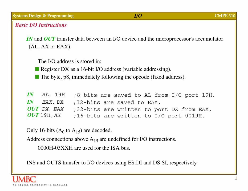
Basic I/O Instructions
IN and OUT transfer data between an I/O device and the microprocessor's accumulator (AL, AX or EAX).
The I/O address is stored in: Register DX as a 16-bit I/O address (variable addressing). The byte, p8, immediately following the opcode (fixed address).
Only 16-bits (A0 to A15) are decoded.
Address connections above A15 are undefined for I/O instructions.
0000H-03XXH are used for the ISA bus.
INS and OUTS transfer to I/O devices using ES:DI and DS:SI, respectively.
IN AL, 19H ;8-bits are saved to AL from I/O port 19H.IN EAX, DX ;32-bits are saved to EAX.OUT DX, EAX ;32-bits are written to port DX from EAX.OUT 19H,AX ;16-bits are written to I/O port 0019H.
2
Systems Design & Programming CMPE 310I/O
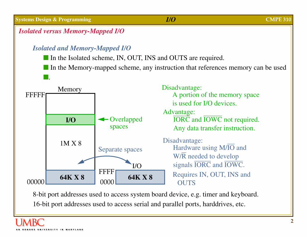
Isolated versus Memory-Mapped I/O
Isolated and Memory-Mapped I/O In the Isolated scheme, IN, OUT, INS and OUTS are required. In the Memory-mapped scheme, any instruction that references memory can be used.
8-bit port addresses used to access system board device, e.g. timer and keyboard.16-bit port addresses used to access serial and parallel ports, harddrives, etc.
00000
FFFFFMemory
1M X 8
0000FFFF
64K X 8
I/O
I/O
64K X 8
Separate spaces
Overlapped
Hardware using M/IO and W/R needed to developsignals IORC and IOWC.Requires IN, OUT, INS and
OUTS
IORC and IOWC not required.Any data transfer instruction.
A portion of the memory spaceis used for I/O devices.
spaces
Disadvantage:
Advantage:
Disadvantage:

3
Systems Design & Programming CMPE 310I/O
I/O Map
0000
I/O Expansion Area
DMA controller
Interrupt controller
Timer
8255(PPI)
COM 2
Hard disk
LPT 1
CGI adapter
Floppy diskCOM 1
FFFF
00100020
00400024
00600044
02F80064
03200300
03780330
03D00380
03F003E0
03F8
Fixed I/O areas
0400
Fixed Port I/O instructions
Variable Port I/O instructions
Computer systemand ISA Bus
PCI Bus, user appsand main-board functions
4
Systems Design & Programming CMPE 310I/O
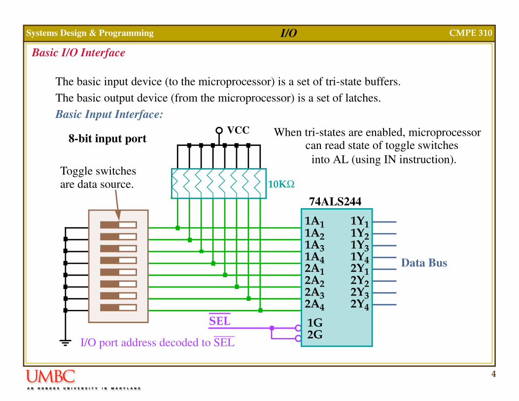
Basic I/O Interface
The basic input device (to the microprocessor) is a set of tri-state buffers.The basic output device (from the microprocessor) is a set of latches.Basic Input Interface:
VCC
Data Bus
SEL
1A11A21A31A42A12A22A32A4
1Y11Y21Y31Y42Y12Y22Y32Y4
1G2G
74ALS244
10KΩ
When tri-states are enabled, microprocessor
Toggle switchesare data source.
8-bit input portcan read state of toggle switches
into AL (using IN instruction).
I/O port address decoded to SEL

5
Systems Design & Programming CMPE 310I/O
Basic I/O Interface
Basic Output Interface:
In this case, the data from the OUT instruction is latched using SEL.
SEL
Data Bus
VCC
330Ω
D0D1D2D3D4D5D6D7
Q0Q1Q2Q3Q4Q5Q6Q7
OC
CLK
U1
D flip-flops hold
Light-emitting diodes emit
74A
LS
374
data from microprocessor
when Q output is 0when Q output is 0
6
Systems Design & Programming CMPE 310I/O
Handshaking
I/O devices are typically slower than the microprocessor.
Handshaking is used to synchronize I/O with the microprocessor.A device indicates that it is ready for a command or data (through some I/O pin or port).
The processor issues a command to the device, and the device indicates it is busy (not ready).
The I/O device finishes its task and indicates a ready condition, and the cycle contin-ues.
There are two basic mechanisms for the processor to service a device. Polling: Processor initiated. Device indicates it is ready by setting some status bit
and the processor periodically checks it. Interrupts: Device initiated. The act of setting a status bit causes an interrupt, and the
processor calls an ISR to service the device.
7
Systems Design & Programming CMPE 310I/O
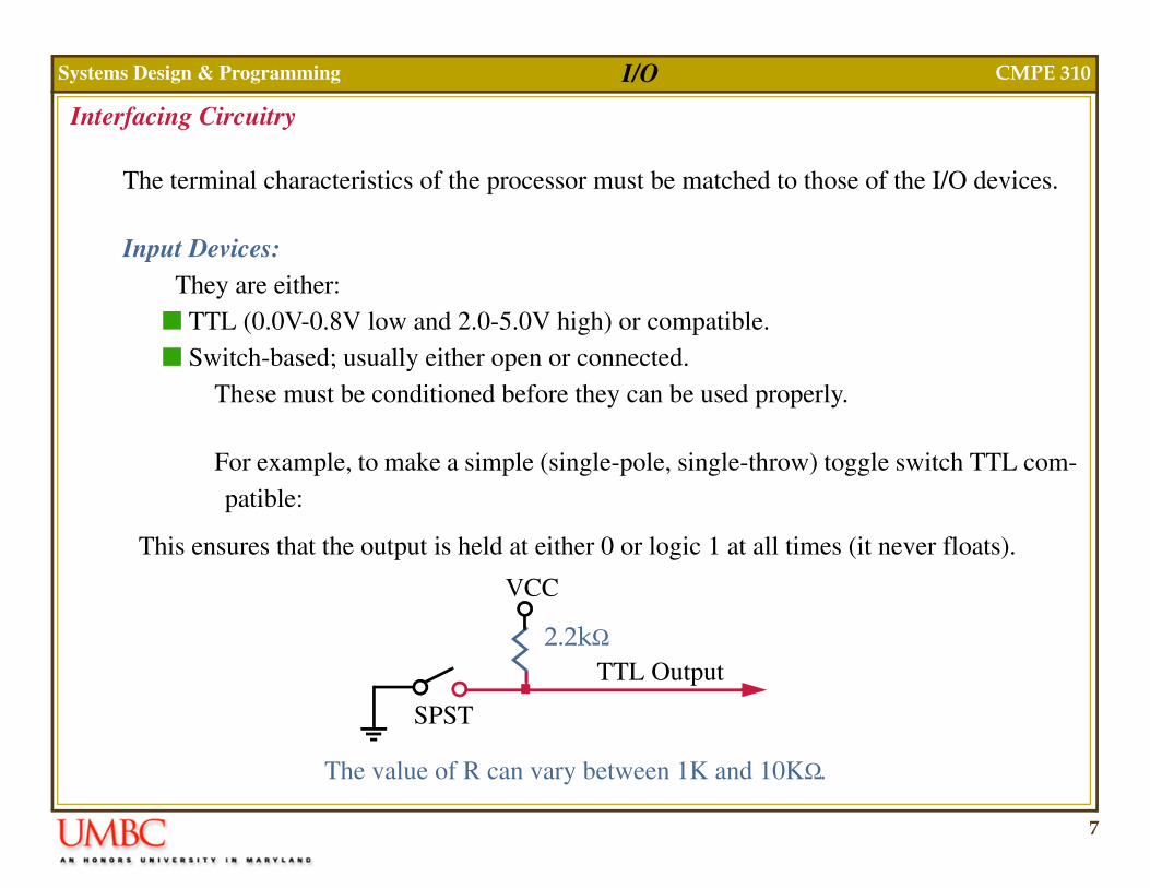
Interfacing Circuitry
The terminal characteristics of the processor must be matched to those of the I/O devices.
Input Devices:They are either: TTL (0.0V-0.8V low and 2.0-5.0V high) or compatible. Switch-based; usually either open or connected.
These must be conditioned before they can be used properly.
For example, to make a simple (single-pole, single-throw) toggle switch TTL com-patible:
2.2kΩ
VCC
TTL Output
SPST
This ensures that the output is held at either 0 or logic 1 at all times (it never floats).
The value of R can vary between 1K and 10KΩ.
8
Systems Design & Programming CMPE 310I/O
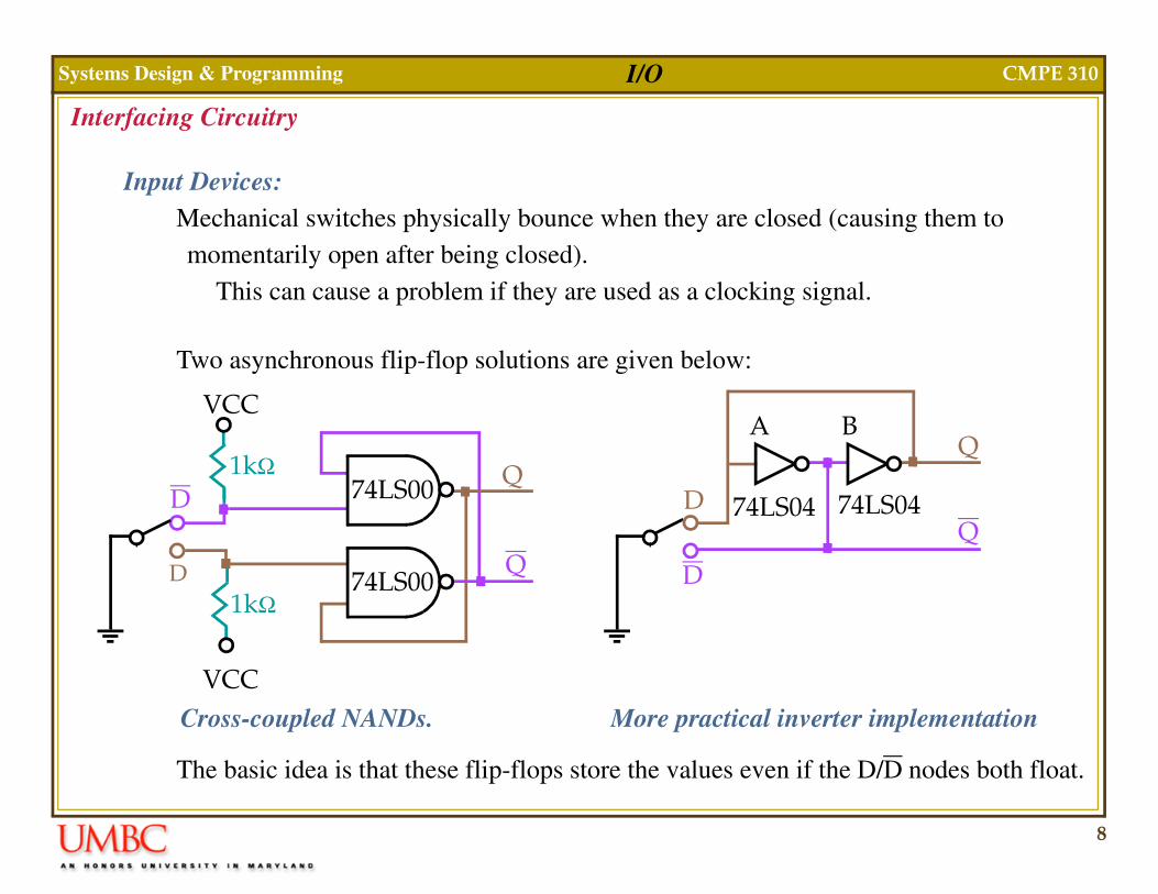
Interfacing Circuitry
Input Devices:Mechanical switches physically bounce when they are closed (causing them to momentarily open after being closed).
This can cause a problem if they are used as a clocking signal.
Two asynchronous flip-flop solutions are given below:
The basic idea is that these flip-flops store the values even if the D/D nodes both float.
VCC
1kΩD
D
VCC
1kΩQ
QD
D
74LS04 74LS04
A B
Q
Q
74LS00
74LS00
Cross-coupled NANDs. More practical inverter implementation
9
Systems Design & Programming CMPE 310I/O
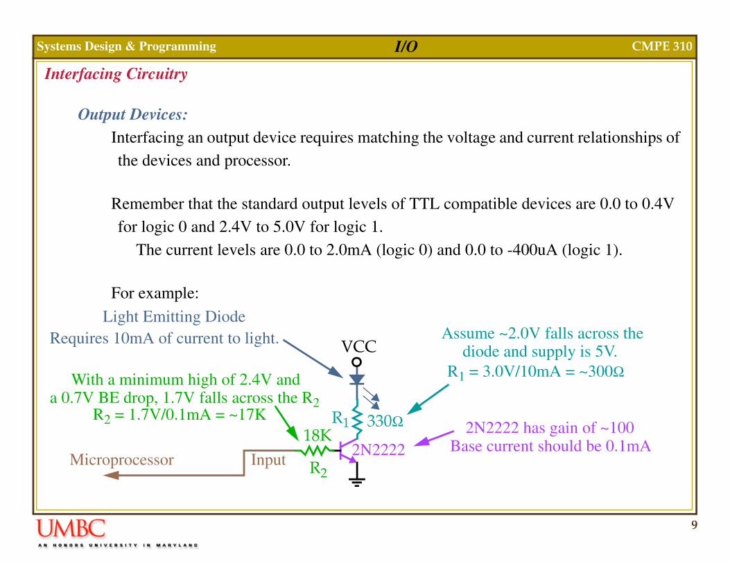
Interfacing Circuitry
Output Devices:Interfacing an output device requires matching the voltage and current relationships of the devices and processor.
Remember that the standard output levels of TTL compatible devices are 0.0 to 0.4V for logic 0 and 2.4V to 5.0V for logic 1.
The current levels are 0.0 to 2.0mA (logic 0) and 0.0 to -400uA (logic 1).
For example:
VCC
330Ω
2N2222Input
Light Emitting Diode
18KMicroprocessor
Requires 10mA of current to light. Assume ~2.0V falls across the
R1 = 3.0V/10mA = ~300Ω
2N2222 has gain of ~100Base current should be 0.1mA
With a minimum high of 2.4V anda 0.7V BE drop, 1.7V falls across the R2
diode and supply is 5V.
R2
R1R2 = 1.7V/0.1mA = ~17K
10
Systems Design & Programming CMPE 310I/O
I/O Port Decoding
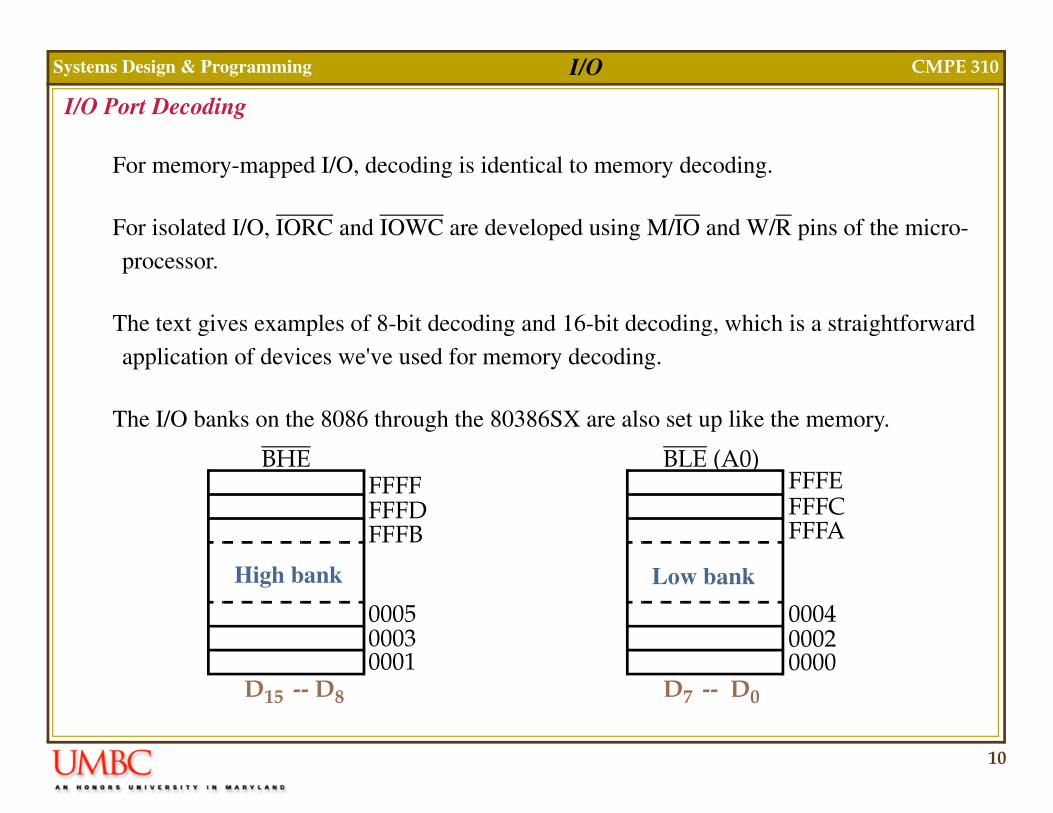
For memory-mapped I/O, decoding is identical to memory decoding.
For isolated I/O, IORC and IOWC are developed using M/IO and W/R pins of the micro-processor.
The text gives examples of 8-bit decoding and 16-bit decoding, which is a straightforward application of devices we've used for memory decoding.
The I/O banks on the 8086 through the 80386SX are also set up like the memory.
FFFFFFFD
00030001
D15 -- D8
FFFEFFFC
00020000
D7 -- D0
High bank
BHE BLE (A0)
FFFB
0005
Low bank
FFFA
0004
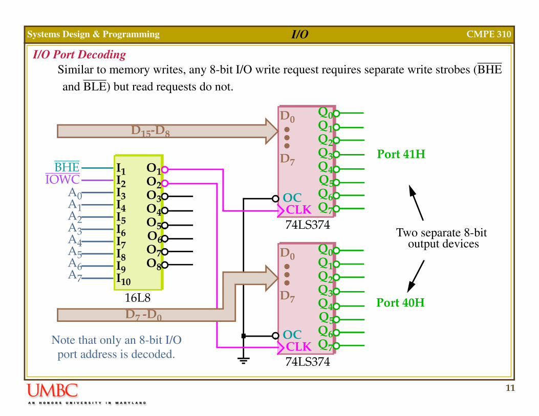
11
Systems Design & Programming CMPE 310I/O
I/O Port DecodingSimilar to memory writes, any 8-bit I/O write request requires separate write strobes (BHE and BLE) but read requests do not.
OCCLK74LS374
A0
BHEIOWC
Port 40H
Port 41HO1O2O3O4O5O6O7O8
16L8
I1I2I3I4I5I6I7I8I9I10
A1A2A3A4A5A6A7
Q0Q1Q2Q3Q4Q5Q6Q7
D0
D7
OCCLK74LS374
Q0Q1Q2Q3Q4Q5Q6Q7
D0
D7
D7 -D0
D15-D8
Two separate 8-bit
Note that only an 8-bit I/Oport address is decoded.
output devices

12
Systems Design & Programming CMPE 310I/O
I/O Port Decoding
Output devices can be 16-bit in which case BHE is not needed.
Input devices can be 8-bit or 16-bit.Note that instead of latches, high impedance buffers (74ALS244) are used in these cases.
32-bit ports are becoming more popular because of PCI bus primarily.The EISA and VESA local bus are also 32-bit buses.
For the 64-bit data buses of the Pentium, the I/O ports can appear in any of the 8 banks.However, only 32-bit transfers are supported, as there are no 64-bit transfer instruc-tions.
13
Systems Design & Programming CMPE 310I/O
Programmable Peripheral Interface (82C55)
The 82C55 is a popular interfacing component, that can interface any TTL-compatible I/O device to the microprocessor.
It is used to interface to the keyboard and a parallel printer port in PCs (usually as part of an integrated chipset).
Requires insertion of wait states if used with a microprocessor using higher that an 8 MHz clock.
PPI has 24 pins for I/O that are programmable in groups of 12 pins and has three distinct modes of operation.
In the PC, an 82C55 or its equivalent is decoded at I/O ports 60H-63H.
14
Systems Design & Programming CMPE 310I/O
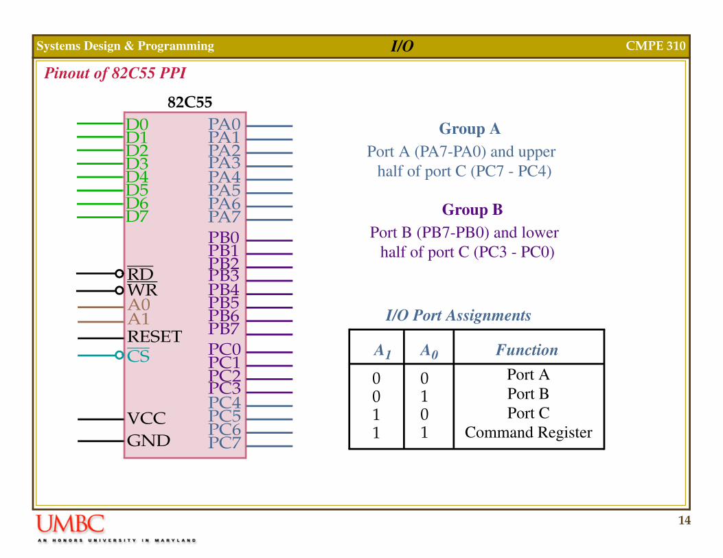
Pinout of 82C55 PPI
D1D2 D3D4D5D6D7
D082C55
RDWRA0A1
CSRESET
VCCGND
A1 A0 Function
0 0 1 1
0101
I/O Port Assignments
Port A (PA7-PA0) and upper half of port C (PC7 - PC4)
Group A
Port B (PB7-PB0) and lower half of port C (PC3 - PC0)
Group B
Port APort BPort C
Command Register
PA1PA2PA3PA4PA5PA6PA7
PA0
PB1PB2PB3PB4PB5PB6PB7
PB0
PC1PC2PC3PC4PC5PC6PC7
PC0
15
Systems Design & Programming CMPE 310I/O
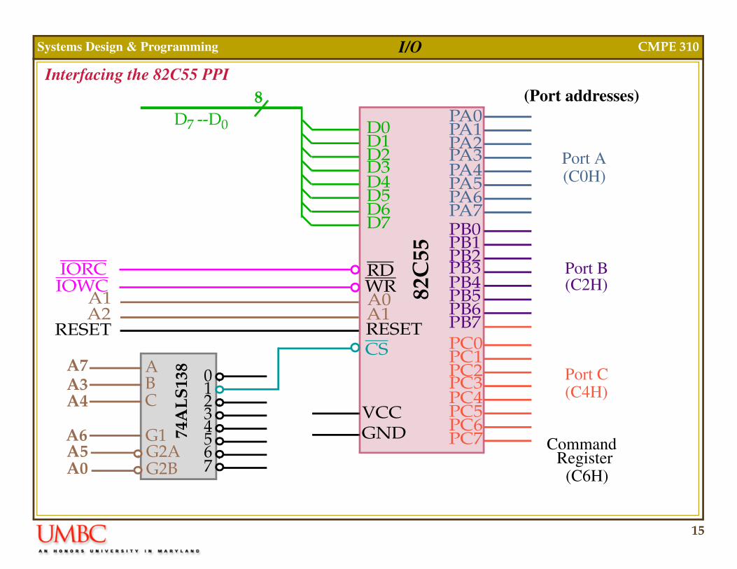
Interfacing the 82C55 PPI
Port A
Port B
Port CA7A3A4
A6A5A0
ABC
G1G2AG2B
01234567
74A
LS
138
IORC IOWC
A1A2
RESET
D1D2D3D4D5D6D7
D0 PA1PA2PA3PA4PA5PA6PA7
PA0
PB1PB2PB3PB4PB5PB6PB7
PB0
PC1PC2PC3PC4PC5PC6PC7
PC0
RDWRA0A1
CSRESET
VCCGND
82C
55
(C0H)
(C2H)
(C4H)
(C6H)
CommandRegister
(Port addresses)D7 --D0
8
16
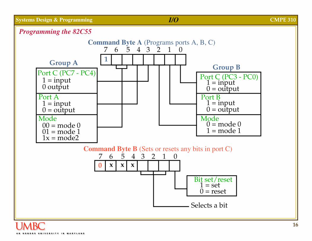
Systems Design & Programming CMPE 310I/O
Programming the 82C55
Port C (PC3 - PC0)1 = input0 = output
Port B 1 = input0 = output
Mode0 = mode 0 1 = mode 1
Mode00 = mode 001 = mode 11x = mode2
Port A 1 = input0 = output
Port C (PC7 - PC4)1 = input0 output
17
Command Byte A (Programs ports A, B, C)
Command Byte B (Sets or resets any bits in port C)
Bit set/reset1 = set0 = reset
Selects a bit
0
Group BGroup A
6 5 4 3 2 1 0
x x x7 6 5 4 3 2 1 0
17
Systems Design & Programming CMPE 310I/O
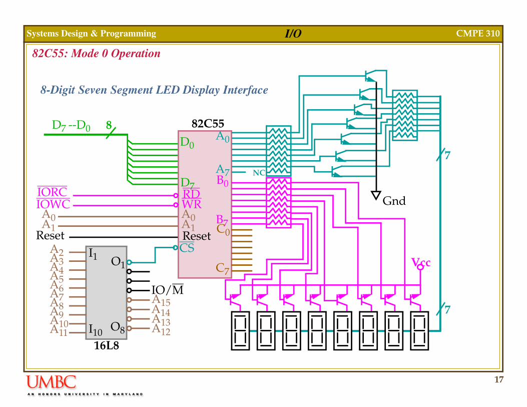
82C55: Mode 0 Operation
D7 --D0 82C55
D0
D7
A0
A7
B7
B0
C7
C0
A0A1Reset
IORCIOWC
7
7
8-Digit Seven Segment LED Display Interface
NC
Vcc
Gnd
16L8
A4A5A6
A8A9
A7
A10 A12
A14A15
A13
IO/M
A11
CS
A0A1
RDWR
ResetI1
I10
O1
O8
A3A2
8
18
Systems Design & Programming CMPE 310I/O
82C55: Mode 0 Operation
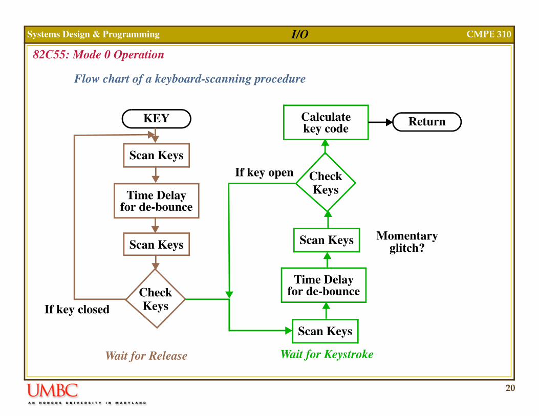
Mode 0 operation causes the 82C55 to function as a buffered input device or as a latched output device.
In previous example, both ports A and B are programmed as (mode 0) simple latched out-put ports.
Port A provides the segment data inputs to display and port B provides a means of selecting one display position at a time.
Different values are displayed in each digit via fast time multiplexing.
The values for the resistors and the type of transistors used are determined using the current requirements (see text for details).
Textbook has the assembly code fragment demonstrating its use.
Examples of connecting LCD displays and stepper motors are also given.
19
Systems Design & Programming CMPE 310I/O
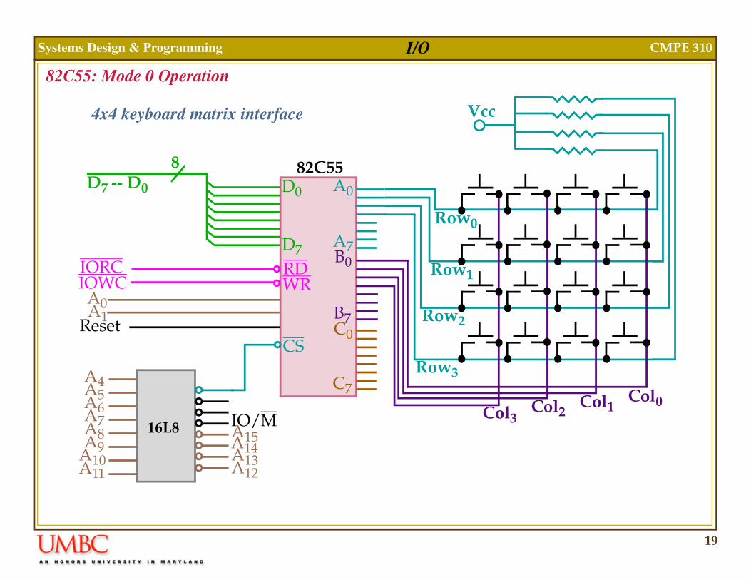
82C55: Mode 0 Operation
D7 -- D082C55
D0
D7
A0
A7
B7
B0
C7
C0
16L8
A0A1
A4A5A6
A8A9
A7
A10 A12
A14A15A13
IO/M
A11
CSReset
IORCIOWC
Row0
Row1
Row2
Row3
Col2Col1
Col0
4x4 keyboard matrix interface
Col3
Vcc
8
RDWR
20
Systems Design & Programming CMPE 310I/O
82C55: Mode 0 Operation
KEY
Scan Keys
Time Delayfor de-bounce
Scan Keys
CheckKeysIf key closed
Scan Keys
Time Delayfor de-bounce
Scan Keys
CheckKeys
Calculatekey code Return
If key open
Flow chart of a keyboard-scanning procedure
Wait for Release Wait for Keystroke
Momentaryglitch?
21
Systems Design & Programming CMPE 310I/O
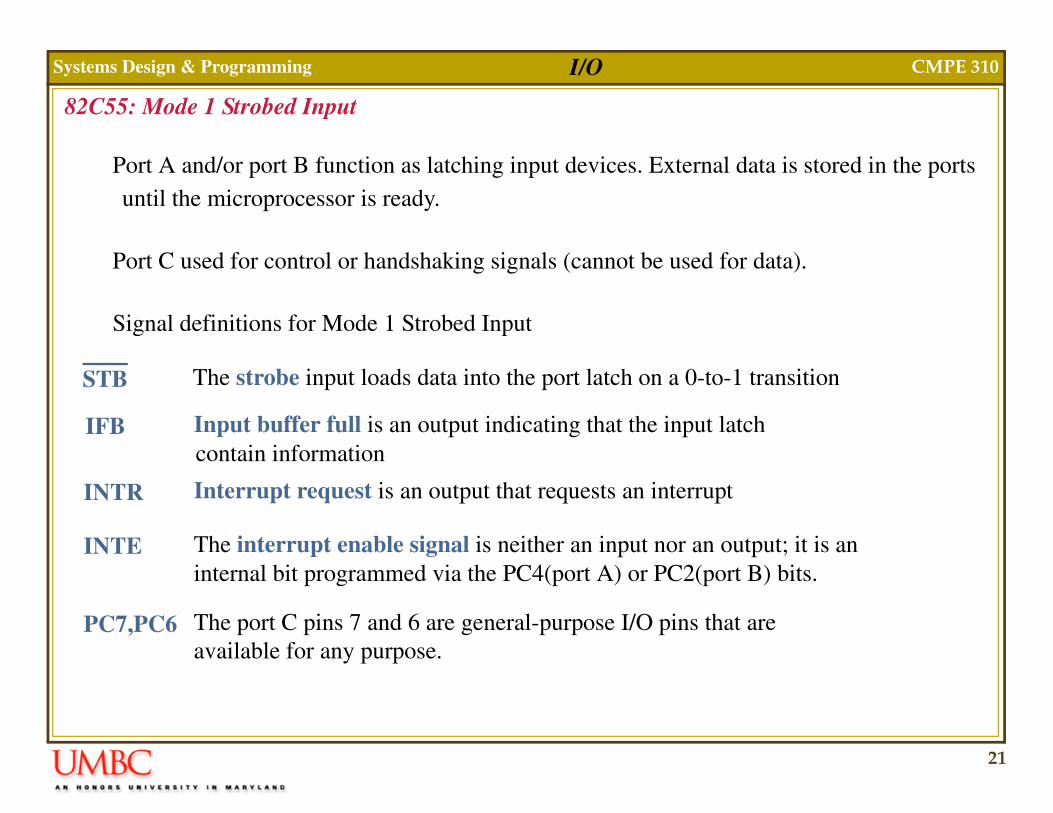
82C55: Mode 1 Strobed Input
Port A and/or port B function as latching input devices. External data is stored in the ports until the microprocessor is ready.
Port C used for control or handshaking signals (cannot be used for data).
Signal definitions for Mode 1 Strobed Input
INTR Interrupt request is an output that requests an interrupt
IFB Input buffer full is an output indicating that the input latchcontain information
STB The strobe input loads data into the port latch on a 0-to-1 transition
INTE The interrupt enable signal is neither an input nor an output; it is aninternal bit programmed via the PC4(port A) or PC2(port B) bits.
PC7,PC6 The port C pins 7 and 6 are general-purpose I/O pins that are available for any purpose.
22
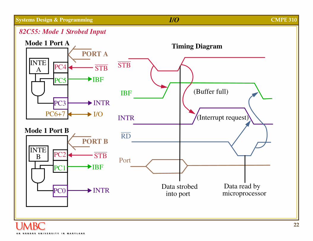
Systems Design & Programming CMPE 310I/O
82C55: Mode 1 Strobed Input
PC5
PC4
PC3
IBF
STB
INTR
I/O
INTEA
PC6+7
PORT A
Mode 1 Port A
PC1
PC2
PC0
IBF
STB
INTR
INTEB
PORT B
Mode 1 Port B
STB
IBF
INTR
RD
Port
(Buffer full)
(Interrupt request)
Data strobed Data read bymicroprocessorinto port
Timing Diagram

23
Systems Design & Programming CMPE 310I/O
82C55: Mode 1 Strobed Output
Similar to Mode 0 output operation, except that handshaking signals are provided using port C.
Signal Definitions for Mode 1 Strobed Output
INTR Interrupt request is an output that requests an interrupt
The acknowledge signal causes the OBF pin to return to 0.This is a response from an external device.
OBF
INTE The interrupt enable signal is neither an input nor an output; it is aninternal bit programmed via the PC6(port A) or PC2(port B) bits.
PC5,PC4 The port C pins 5 and 4 are general-purpose I/O pins that are available for any purpose.
Output buffer full is an output that goes low when data is latchedin either port A or port B. Goes low on ACK.
ACK
24
Systems Design & Programming CMPE 310I/O
82C55: Mode 1 Strobed Output
PC7
PC6
PC3
WR
INTR
I/OPC4+5
PORT A
Mode 1 Port A
PC1
PC2
PC0 INTR
PORT B
Mode 1 Port B
ACK
Timing Diagram
OBF
ACK
OBF
OBF
INTR
ACK
Port
(Buffer full)
(Interrupt request)
Data sent Data removedfrom portto port
INTEA
INTEB
25
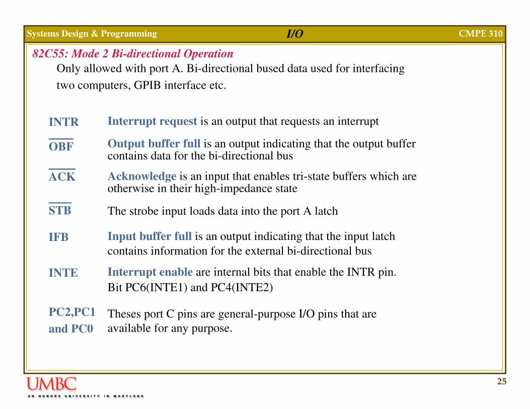
Systems Design & Programming CMPE 310I/O
82C55: Mode 2 Bi-directional OperationOnly allowed with port A. Bi-directional bused data used for interfacingtwo computers, GPIB interface etc.
INTR Interrupt request is an output that requests an interrupt
Acknowledge is an input that enables tri-state buffers which are
OBF
INTE Interrupt enable are internal bits that enable the INTR pin.
PC2,PC1 Theses port C pins are general-purpose I/O pins that are available for any purpose.
Output buffer full is an output indicating that the output buffer
ACK
contains data for the bi-directional bus
otherwise in their high-impedance state
STB The strobe input loads data into the port A latch
IFB Input buffer full is an output indicating that the input latchcontains information for the external bi-directional bus
Bit PC6(INTE1) and PC4(INTE2)
and PC0
26
Systems Design & Programming CMPE 310I/O
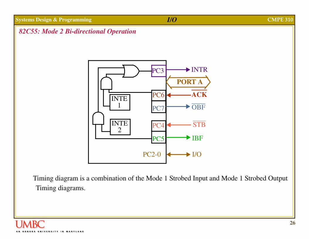
82C55: Mode 2 Bi-directional Operation
Timing diagram is a combination of the Mode 1 Strobed Input and Mode 1 Strobed Output Timing diagrams.
PC7
PC6
PC3 INTR
INTE1
PC2-0
PORT A
ACK
OBF
STB
IBFPC5
PC4INTE2
I/O