basic emission and immunity analysis of a circuit board
TRANSCRIPT

Created in COMSOL Multiphysics 5.6
Ba s i c Em i s s i o n and Immun i t y Ana l y s i s o f a C i r c u i tB o a r d
This model is licensed under the COMSOL Software License Agreement 5.6.All trademarks are the property of their respective owners. See www.comsol.com/trademarks.
Introduction
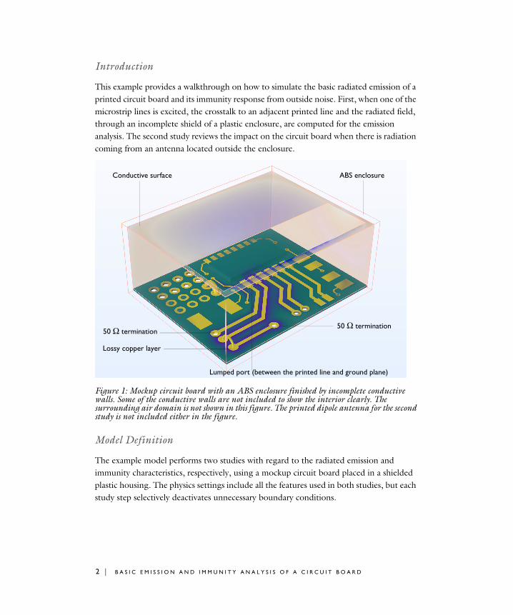
This example provides a walkthrough on how to simulate the basic radiated emission of a printed circuit board and its immunity response from outside noise. First, when one of the microstrip lines is excited, the crosstalk to an adjacent printed line and the radiated field, through an incomplete shield of a plastic enclosure, are computed for the emission analysis. The second study reviews the impact on the circuit board when there is radiation coming from an antenna located outside the enclosure.
Figure 1: Mockup circuit board with an ABS enclosure finished by incomplete conductive walls. Some of the conductive walls are not included to show the interior clearly. The surrounding air domain is not shown in this figure. The printed dipole antenna for the second study is not included either in the figure.
Model Definition
The example model performs two studies with regard to the radiated emission and immunity characteristics, respectively, using a mockup circuit board placed in a shielded plastic housing. The physics settings include all the features used in both studies, but each study step selectively deactivates unnecessary boundary conditions.
ABS enclosure
50 Ω termination50 Ω termination
Lumped port (between the printed line and ground plane)
Conductive surface
Lossy copper layer
2 | B A S I C E M I S S I O N A N D I M M U N I T Y A N A L Y S I S O F A C I R C U I T B O A R D

Here is the list of all the physics features (boundary conditions), in addition to the default features:
The mockup circuit board is made out of the FR4 material, and the printed circuit pattern is defined by a copper layer. To capture the loss that is caused by the finite conductivity in the geometrically thin copper layer, a transition boundary condition is used. The thickness of the conductive layer is set to 30 um. The circuit board is placed in the ABS plastic housing, where the interior walls are finished by the perfect electric conductor (PEC) feature. However, the conductive surface is not completely finished and has a small window on the top of the enclosure. The radiated emission from the circuit board is leaked through this window. The amount of radiation is computed in terms of the near-field distribution as well as the far-field radiation. There is a printed dipole antenna outside the housing, and its resonance is around the Wi-Fi frequency range. The air domain encloses all the items mentioned earlier, and a scattering boundary condition is assigned on the exterior boundaries of the air domain. The scattering boundary condition absorbs all outgoing radiation, and the incident waves on the outer boundaries won’t be reflected back to the source.
E M I S S I O N T E S T
One of the microstrip lines in the circuit board is excited using a uniform lumped port. The crosstalk between this signal path and another line is examined. Impedance mismatching, resonances of the copper traces, or resonances from the incompletely shielded cavity can be a source of radiated emission once they are excited. The source-
TABLE 1: PHYSICS FEATURE LIST
FEATURES PURPOSE STUDY 1 STUDY 2
Lumped Port 1 Microstrip line excitation Disabled
Lumped Port 2 Dipole antenna excitation Disabled
Lumped Element 1 50 Ω via termination
Lumped Element 2 50 Ω via termination
Transition Boundary Condition 1 Lossy copper surfaces
Perfect Electric Conductor 2 Printed dipole strip, lossless Disabled
Perfect Electric Conductor 3 Metalized vias, lossless
Perfect Electric Conductor 4 Jumpers, lossless
Perfect Electric Conductor 5 Shielded interior walls, lossless
Scattering Boundary Condition 1 Absorbing boundaries
Far-Field Domain 1 and Far-Field Calculation 1
Near-field to far-field transformation
Disabled
3 | B A S I C E M I S S I O N A N D I M M U N I T Y A N A L Y S I S O F A C I R C U I T B O A R D

driven field is radiated via the top window. The near field and the transformed far field on the exterior boundaries are computed to evaluate the radiated emission.
I M M U N I T Y T E S T
The second study mimics the concept of immunity tests. The source is located outside the enclosure, and the victim is the circuit board with the incompletely shielded case. A printed dipole antenna resonant around the Wi-Fi frequency is excited. The antenna radiation is coupled to the circuit board through the open window. The electric field illuminated over the circuit board and the coupled power ratio, between the antenna input and the metalized via of a selected microstrip line, is computed.
Results and Discussion
The primary emission and immunity simulations are performed in separate studies. In Figure 2, the electric field norm is plotted in the dB scale with three color tables to emphasize the visual effect. When the selected line is excited, the strongest field (light yellow from the HeatCameraLight color table) is observed over the signal path. The surfaces of the FR4 board are visualized with the AuroraAustralis color table. The strongly coupled field is expressed as the blueish violet color that can be seen around all adjacent microstrip lines as well as the excited signal path. The Twilight color table is used to plot
4 | B A S I C E M I S S I O N A N D I M M U N I T Y A N A L Y S I S O F A C I R C U I T B O A R D

the field on the interior boundaries of the plastic housing and the open window. The legend is activated only for the field plot on the signal path.
Figure 2: Three color tables are used for the electric field norm plot in the dB scale: HeatCameraLight, AuroraAustralis, and Twilight, respectively.
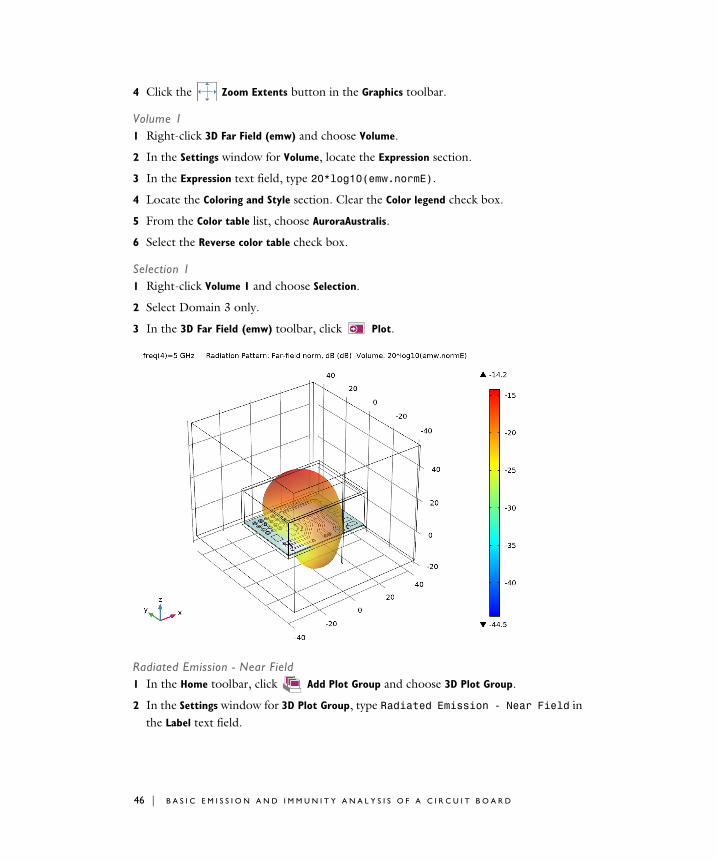
The directional field strength of the radiated emission is shown as a 3D far-field pattern in Figure 3. At 5 GHz, the strongest far field is generated. The far-field radiation pattern is
Excited signal path
5 | B A S I C E M I S S I O N A N D I M M U N I T Y A N A L Y S I S O F A C I R C U I T B O A R D

plotted partially transparent not to block the view of the circuit board. The depth of the transparency is controlled by the Transparency subfeature.
Figure 3: Radiated emission in terms of far-field radiation at 5 GHz. The electric field norm of the circuit board is also plotted with the dB scale.
For the computation of the total radiated emission, the time-averaged power outflow is integrated over the exterior boundaries. Figure 4 shows the ratio between the power outflow and the input power. Figure 5 shows the crosstalk between the signal path and an adjacent microstrip line. The crosstalk here is the power ratio - the power at the metalized via connected to the adjacent microstrip line normalized by the input power.
6 | B A S I C E M I S S I O N A N D I M M U N I T Y A N A L Y S I S O F A C I R C U I T B O A R D

Figure 4: Leaked power ratio - the power outflow through the exterior boundaries normalized by the input power.
Figure 5: Crosstalk ratio, the coupled power (adjacent line) to the input power (signal path).
7 | B A S I C E M I S S I O N A N D I M M U N I T Y A N A L Y S I S O F A C I R C U I T B O A R D

Figure 6 describes how much the noise from outside can impact on the signal path with an open end. The maximum coupling is observed at 5 GHz.
Figure 6: Impact on the microstrip line due to the radiation from the outside.
While the printed dipole antenna is supposed to work well at the Wi-Fi frequency, the maximum coupling does not occur around that frequency. The length of the signal path is about one wavelength at 5 GHz. So it could be more susceptible around 5 GHz. Another reason would be the resonance from the cavity formed by the shielded walls.
The resonant frequency of a rectangular cavity is
where a and b are the dimensions of the sidewall of the cavity and d is the length of the cavity. For this example, the dominant resonant frequency at TE101 mode is close to 4.8 GHz. Because the cavity is not entirely closed and partially filled by the circuit board with metal strips, this estimation gives only an approximated value but a good clue for the susceptibility as a function of frequency.
fnmlc
2π εrμr
---------------------- mπa-------- 2 nπ
b------- 2 lπ
d----- 2
+ +=
8 | B A S I C E M I S S I O N A N D I M M U N I T Y A N A L Y S I S O F A C I R C U I T B O A R D

Notes About the COMSOL Implementation
This example provides only a simplified modeling workflow for the virtual emission and immunity tests. It does not comply with the well-known test standards and protocols. The model setup has to be modified accordingly to perform the standard test.
Application Library path: RF_Module/EMI_EMC_Applications/circuit_emiemc
Modeling Instructions
From the File menu, choose New.
N E W
In the New window, click Model Wizard.
M O D E L W I Z A R D
1 In the Model Wizard window, click 3D.
2 In the Select Physics tree, select Radio Frequency>Electromagnetic Waves,
Frequency Domain (emw).
3 Click Add.
4 Click Study.
5 In the Select Study tree, select General Studies>Frequency Domain.
6 Click Done.
G E O M E T R Y 1
1 In the Model Builder window, under Component 1 (comp1) click Geometry 1.
2 In the Settings window for Geometry, locate the Units section.
3 From the Length unit list, choose mm.
Import 1 (imp1)1 In the Home toolbar, click Import.
First, import a mockup circuit board.
2 In the Settings window for Import, locate the Import section.
3 Click Browse.
9 | B A S I C E M I S S I O N A N D I M M U N I T Y A N A L Y S I S O F A C I R C U I T B O A R D
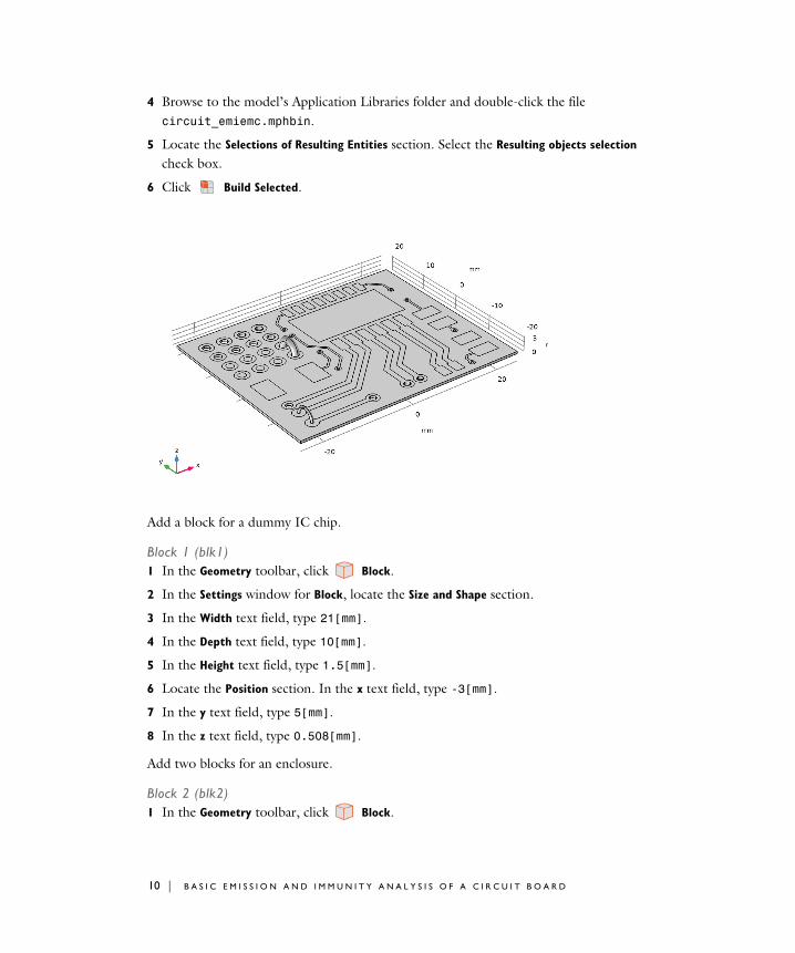
4 Browse to the model’s Application Libraries folder and double-click the file circuit_emiemc.mphbin.
5 Locate the Selections of Resulting Entities section. Select the Resulting objects selection check box.
6 Click Build Selected.
Add a block for a dummy IC chip.
Block 1 (blk1)1 In the Geometry toolbar, click Block.
2 In the Settings window for Block, locate the Size and Shape section.
3 In the Width text field, type 21[mm].
4 In the Depth text field, type 10[mm].
5 In the Height text field, type 1.5[mm].
6 Locate the Position section. In the x text field, type -3[mm].
7 In the y text field, type 5[mm].
8 In the z text field, type 0.508[mm].
Add two blocks for an enclosure.
Block 2 (blk2)1 In the Geometry toolbar, click Block.
10 | B A S I C E M I S S I O N A N D I M M U N I T Y A N A L Y S I S O F A C I R C U I T B O A R D
2 In the Settings window for Block, locate the Size and Shape section.
3 In the Width text field, type 50[mm].
4 In the Depth text field, type 40[mm].
5 In the Height text field, type 20[mm].
6 Locate the Position section. From the Base list, choose Center.
7 In the z text field, type 10[mm].
8 Click Build Selected.
9 Click the Wireframe Rendering button in the Graphics toolbar.
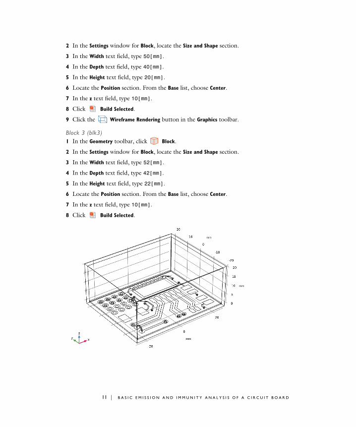
Block 3 (blk3)1 In the Geometry toolbar, click Block.
2 In the Settings window for Block, locate the Size and Shape section.
3 In the Width text field, type 52[mm].
4 In the Depth text field, type 42[mm].
5 In the Height text field, type 22[mm].
6 Locate the Position section. From the Base list, choose Center.
7 In the z text field, type 10[mm].
8 Click Build Selected.
11 | B A S I C E M I S S I O N A N D I M M U N I T Y A N A L Y S I S O F A C I R C U I T B O A R D

Work Plane 1 (wp1)1 In the Geometry toolbar, click Work Plane.
2 In the Settings window for Work Plane, locate the Plane Definition section.
3 From the Plane type list, choose Face parallel.
4 On the object blk2, select Boundary 4 only.
Work Plane 1 (wp1)>Plane GeometryIn the Model Builder window, click Plane Geometry.
Work Plane 1 (wp1)>Rectangle 1 (r1)1 In the Work Plane toolbar, click Rectangle.
2 In the Settings window for Rectangle, locate the Size and Shape section.
3 In the Width text field, type 48[mm].
4 In the Height text field, type 14[mm].
5 Locate the Position section. In the xw text field, type -24[mm].
6 In the yw text field, type 4[mm].
12 | B A S I C E M I S S I O N A N D I M M U N I T Y A N A L Y S I S O F A C I R C U I T B O A R D

7 Click Build Selected.
This geometry describes an open window on the top side of the enclosure.
Difference 1 (dif1)1 In the Model Builder window, right-click Geometry 1 and choose
Booleans and Partitions>Difference.
2 Select the object blk2 only.
3 In the Settings window for Difference, locate the Difference section.
4 Find the Objects to subtract subsection. Select the Activate Selection toggle button.
5 Select the object blk1 only.
6 Click Build Selected.
Add a block for the surrounding air domain.
Block 4 (blk4)1 In the Geometry toolbar, click Block.
2 In the Settings window for Block, locate the Size and Shape section.
3 In the Width text field, type 80[mm].
4 In the Depth text field, type 90[mm].
5 In the Height text field, type 70[mm].
6 Locate the Position section. From the Base list, choose Center.
13 | B A S I C E M I S S I O N A N D I M M U N I T Y A N A L Y S I S O F A C I R C U I T B O A R D

7 In the z text field, type 20[mm].
8 Click Build Selected.
The following 2D geometry is for a printed dipole antenna.
Work Plane 2 (wp2)1 In the Geometry toolbar, click Work Plane.
2 In the Settings window for Work Plane, locate the Plane Definition section.
3 From the Plane list, choose yz-plane.
Work Plane 2 (wp2)>Plane GeometryIn the Model Builder window, click Plane Geometry.
Work Plane 2 (wp2)>Rectangle 1 (r1)1 In the Work Plane toolbar, click Rectangle.
2 In the Settings window for Rectangle, locate the Size and Shape section.
3 In the Width text field, type 1.
4 In the Height text field, type 55[mm]. The size is approximated for the antenna operating at the Wi-Fi frequency range
5 Locate the Position section. From the Base list, choose Center.
6 In the xw text field, type -33[mm].
7 In the yw text field, type 20[mm].
14 | B A S I C E M I S S I O N A N D I M M U N I T Y A N A L Y S I S O F A C I R C U I T B O A R D

8 Click to expand the Layers section. In the table, enter the following settings:
9 Select the Layers on top check box.
Note that both Layers on bottom and Layers on top are checked. This creates a small rectangle in the middle of the strip where a lumped port will be assigned to excite the printed dipole antenna.
Add a small rectangular boundary for the lumped port to excite one of the printed lines on the circuit board.
Work Plane 3 (wp3)1 In the Model Builder window, right-click Geometry 1 and choose Work Plane.
2 In the Settings window for Work Plane, locate the Plane Definition section.
3 From the Plane list, choose zx-plane.
4 In the y-coordinate text field, type 4.
Work Plane 3 (wp3)>Plane GeometryIn the Model Builder window, click Plane Geometry.
Work Plane 3 (wp3)>Rectangle 1 (r1)1 In the Work Plane toolbar, click Rectangle.
2 In the Settings window for Rectangle, locate the Size and Shape section.
3 In the Width text field, type 0.508[mm].
4 In the Height text field, type 2[mm].
5 Locate the Position section. In the yw text field, type 2[mm].
Layer name Thickness (mm)
Layer 1 27[mm]
15 | B A S I C E M I S S I O N A N D I M M U N I T Y A N A L Y S I S O F A C I R C U I T B O A R D

6 Click Build Selected.
7 In the Model Builder window, right-click Geometry 1 and choose Build All.
8 Click the Zoom Extents button in the Graphics toolbar.
Define selections that are useful for configuring physics settings, material properties, and results analysis later on.
16 | B A S I C E M I S S I O N A N D I M M U N I T Y A N A L Y S I S O F A C I R C U I T B O A R D

D E F I N I T I O N S
Printed layer1 In the Definitions toolbar, click Explicit.
2 In the Settings window for Explicit, type Printed layer in the Label text field.
3 Locate the Input Entities section. From the Geometric entity level list, choose Boundary.
Use the Select Box feature in the graphics window to include multiple boundaries in a selection.
4 Click the Select Box button in the Graphics toolbar.
5 Select Boundaries 21–25, 34–36, 54–57, 70–73, 86–90, 114, 115, 144, 145, 152, 153, 159–165, 169, and 172–174 only.
Vias1 In the Definitions toolbar, click Explicit.
2 In the Settings window for Explicit, type Vias in the Label text field.
3 Locate the Input Entities section. From the Geometric entity level list, choose Boundary.
Choose all cylindrical boundaries of metalized vias.
4 Select the Group by continuous tangent check box.
With Group by continuous tangent, you can select the curved cylindrical surface of a metalized via by selecting one of its boundary elements. The Group by continuous
tangent allows you to select adjacent faces or edges that are continuously tangent with
17 | B A S I C E M I S S I O N A N D I M M U N I T Y A N A L Y S I S O F A C I R C U I T B O A R D

the angular tolerance you specified. Select any part of the cylindrical surfaces of each via, and it will automatically select all surfaces within the angular tolerance range.
5 Select Boundaries 28, 29, 31, 32, 37–42, 52, 53, 60, 61, 63, 64, 66–69, 76, 77, 79, 80, 82–85, 95, 96, 98, 99, 105–110, 112, 113, 116, 117, 119, 120, 122, 123, 125–132, 134, 135, 146, 147, 149, 150, 154, 157, 158, 166, 167, 170, 171, 176, 177, 179, 180, 182, 183, and 185–190 only. These are all via boundaries.
Jumpers1 In the Definitions toolbar, click Explicit.
2 In the Settings window for Explicit, type Jumpers in the Label text field.
3 Locate the Input Entities section. From the Geometric entity level list, choose Boundary.
4 Select the Group by continuous tangent check box.
With Group by continuous tangent, you can select the curved surface of the mockup jumpers easily. Select any surface of each jumper, and it will automatically select all surfaces within the angular tolerance range.
18 | B A S I C E M I S S I O N A N D I M M U N I T Y A N A L Y S I S O F A C I R C U I T B O A R D

5 Select Boundaries 44–51, 91–94, and 101–104 only.
Specify the material properties for the air, circuit board, printed layer, enclosure, and chip.
A D D M A T E R I A L
1 In the Home toolbar, click Add Material to open the Add Material window.
2 Go to the Add Material window.
3 In the tree, select Built-in>Air.
4 Click Add to Component in the window toolbar.
5 In the tree, select Built-in>FR4 (Circuit Board).
6 Click Add to Component in the window toolbar.
19 | B A S I C E M I S S I O N A N D I M M U N I T Y A N A L Y S I S O F A C I R C U I T B O A R D

M A T E R I A L S
FR4 (Circuit Board) (mat2)Select Domain 3 only.
A D D M A T E R I A L
1 Go to the Add Material window.
2 In the tree, select Built-in>Copper.
3 Click Add to Component in the window toolbar.
4 In the Home toolbar, click Add Material to close the Add Material window.
M A T E R I A L S
Copper - printed layer1 In the Settings window for Material, type Copper - printed layer in the Label text
field.
2 Locate the Geometric Entity Selection section. From the Geometric entity level list, choose Boundary.
20 | B A S I C E M I S S I O N A N D I M M U N I T Y A N A L Y S I S O F A C I R C U I T B O A R D
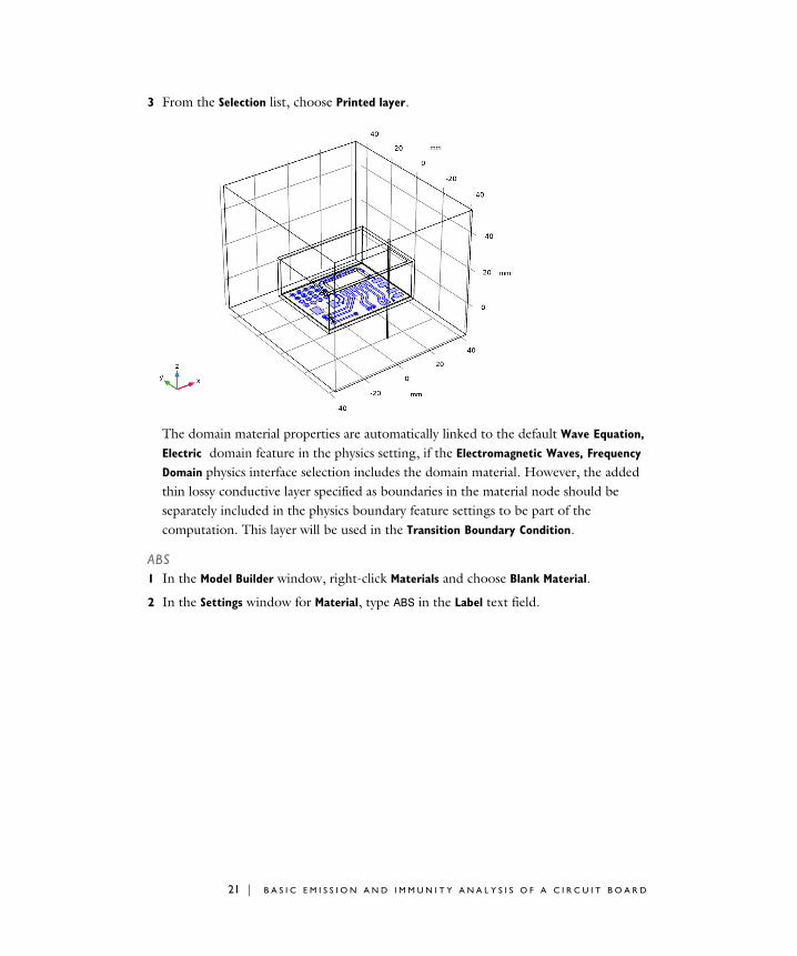
3 From the Selection list, choose Printed layer.
The domain material properties are automatically linked to the default Wave Equation,
Electric domain feature in the physics setting, if the Electromagnetic Waves, Frequency
Domain physics interface selection includes the domain material. However, the added thin lossy conductive layer specified as boundaries in the material node should be separately included in the physics boundary feature settings to be part of the computation. This layer will be used in the Transition Boundary Condition.
ABS1 In the Model Builder window, right-click Materials and choose Blank Material.
2 In the Settings window for Material, type ABS in the Label text field.
21 | B A S I C E M I S S I O N A N D I M M U N I T Y A N A L Y S I S O F A C I R C U I T B O A R D

3 Select Domain 2 only.
4 Locate the Material Contents section. In the table, enter the following settings:
Chip1 Right-click Materials and choose Blank Material.
2 In the Settings window for Material, type Chip in the Label text field.
Property Variable Value Unit Property group
Relative permittivity epsilonr_iso ; epsilonrii = epsilonr_iso, epsilonrij = 0
2.9 1 Basic
Relative permeability mur_iso ; murii = mur_iso, murij = 0
1 1 Basic
Electrical conductivity sigma_iso ; sigmaii = sigma_iso, sigmaij = 0
0 S/m Basic
22 | B A S I C E M I S S I O N A N D I M M U N I T Y A N A L Y S I S O F A C I R C U I T B O A R D

3 Select Domain 5 only.
4 Locate the Material Contents section. In the table, enter the following settings:
The physics settings include the default governing equation - the vector Helmholtz wave equation. Define lumped ports to excite the circuit or the printed antenna in the air. Add a lossy copper layer, lossless conductive boundaries, and 50 ohm terminations. Use absorbing boundaries to truncate the infinite surrounding open space. The postprocessing feature will address the far-field radiation from the circuit board.
Property Variable Value Unit Property group
Relative permittivity epsilonr_iso ; epsilonrii = epsilonr_iso, epsilonrij = 0
12 1 Basic
Relative permeability mur_iso ; murii = mur_iso, murij = 0
1 1 Basic
Electrical conductivity sigma_iso ; sigmaii = sigma_iso, sigmaij = 0
0 S/m Basic
23 | B A S I C E M I S S I O N A N D I M M U N I T Y A N A L Y S I S O F A C I R C U I T B O A R D

E L E C T R O M A G N E T I C W A V E S , F R E Q U E N C Y D O M A I N ( E M W )
Lumped Port 11 In the Model Builder window, under Component 1 (comp1) right-click
Electromagnetic Waves, Frequency Domain (emw) and choose Lumped Port.
2 Select Boundary 151 only.
This lumped port is used to excite the circuit board in the first analysis assuming that the signal trace is a noise source. This feature is activated only in the first emission study using the Modify model configuration for study step option.
Lumped Port 21 In the Physics toolbar, click Boundaries and choose Lumped Port.
24 | B A S I C E M I S S I O N A N D I M M U N I T Y A N A L Y S I S O F A C I R C U I T B O A R D
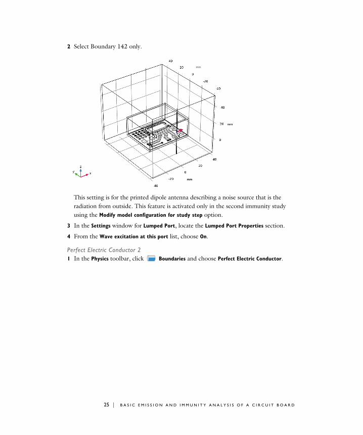
2 Select Boundary 142 only.
This setting is for the printed dipole antenna describing a noise source that is the radiation from outside. This feature is activated only in the second immunity study using the Modify model configuration for study step option.
3 In the Settings window for Lumped Port, locate the Lumped Port Properties section.
4 From the Wave excitation at this port list, choose On.
Perfect Electric Conductor 21 In the Physics toolbar, click Boundaries and choose Perfect Electric Conductor.
25 | B A S I C E M I S S I O N A N D I M M U N I T Y A N A L Y S I S O F A C I R C U I T B O A R D
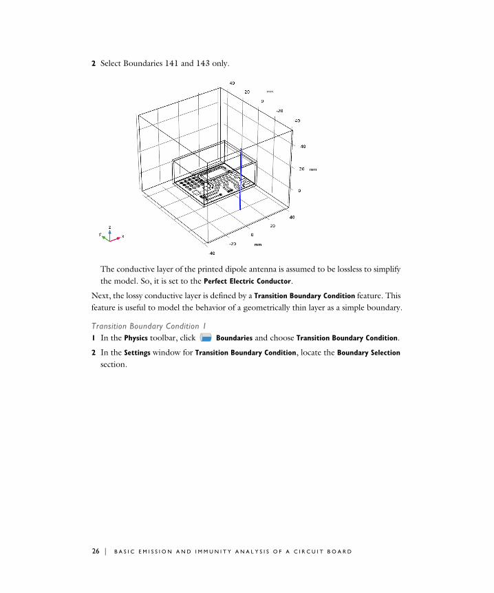
2 Select Boundaries 141 and 143 only.
The conductive layer of the printed dipole antenna is assumed to be lossless to simplify the model. So, it is set to the Perfect Electric Conductor.
Next, the lossy conductive layer is defined by a Transition Boundary Condition feature. This feature is useful to model the behavior of a geometrically thin layer as a simple boundary.
Transition Boundary Condition 11 In the Physics toolbar, click Boundaries and choose Transition Boundary Condition.
2 In the Settings window for Transition Boundary Condition, locate the Boundary Selection section.
26 | B A S I C E M I S S I O N A N D I M M U N I T Y A N A L Y S I S O F A C I R C U I T B O A R D
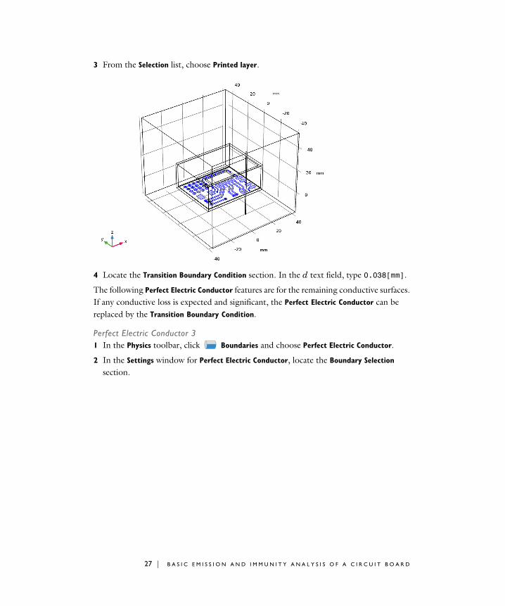
3 From the Selection list, choose Printed layer.
4 Locate the Transition Boundary Condition section. In the d text field, type 0.038[mm].
The following Perfect Electric Conductor features are for the remaining conductive surfaces. If any conductive loss is expected and significant, the Perfect Electric Conductor can be replaced by the Transition Boundary Condition.
Perfect Electric Conductor 31 In the Physics toolbar, click Boundaries and choose Perfect Electric Conductor.
2 In the Settings window for Perfect Electric Conductor, locate the Boundary Selection section.
27 | B A S I C E M I S S I O N A N D I M M U N I T Y A N A L Y S I S O F A C I R C U I T B O A R D

3 From the Selection list, choose Vias.
Perfect Electric Conductor 41 In the Physics toolbar, click Boundaries and choose Perfect Electric Conductor.
2 In the Settings window for Perfect Electric Conductor, locate the Boundary Selection section.
28 | B A S I C E M I S S I O N A N D I M M U N I T Y A N A L Y S I S O F A C I R C U I T B O A R D

3 From the Selection list, choose Jumpers.
Perfect Electric Conductor 51 In the Physics toolbar, click Boundaries and choose Perfect Electric Conductor.
29 | B A S I C E M I S S I O N A N D I M M U N I T Y A N A L Y S I S O F A C I R C U I T B O A R D

2 Select Boundaries 11–15, 17–19, 191, and 192 only.
The interior walls of the enclosure are also finished by the conductive material (PEC). Note that there is a window on the top side.
Lumped Element 11 In the Physics toolbar, click Boundaries and choose Lumped Element.
Use Lumped Element features to describe passive terminations as necessary. Numerically, it is the same as the Lumped Port without wave excitation, but it does not calculate S-parameters.
30 | B A S I C E M I S S I O N A N D I M M U N I T Y A N A L Y S I S O F A C I R C U I T B O A R D

2 Select Boundaries 109, 110, 112, and 113 only.
3 In the Settings window for Lumped Element, locate the Lumped Element Properties section.
4 From the Type of lumped element list, choose Via.
Lumped Element 21 In the Physics toolbar, click Boundaries and choose Lumped Element.
31 | B A S I C E M I S S I O N A N D I M M U N I T Y A N A L Y S I S O F A C I R C U I T B O A R D

2 Select Boundaries 41, 42, 52, and 53 only.
3 In the Settings window for Lumped Element, locate the Lumped Element Properties section.
4 From the Type of lumped element list, choose Via.
Scattering Boundary Condition 11 In the Physics toolbar, click Boundaries and choose Scattering Boundary Condition.
Add a Scattering Boundary Condition that is the first order absorbing boundary condition by default.
32 | B A S I C E M I S S I O N A N D I M M U N I T Y A N A L Y S I S O F A C I R C U I T B O A R D

2 Select Boundaries 1–5 and 194 only.
Far-Field Domain and Far-Field Calculation features are used to compute the far-field radiation from the excited signal trace. These are activated only in the first emission study using the Modify model configuration for study step option.
Far-Field Domain 11 In the Physics toolbar, click Domains and choose Far-Field Domain.
2 In the Settings window for Far-Field Domain, locate the Domain Selection section.
3 Click Clear Selection.
33 | B A S I C E M I S S I O N A N D I M M U N I T Y A N A L Y S I S O F A C I R C U I T B O A R D

4 Select Domain 1 only.
The selection of the Far-Field Domain feature should include a homogeneous medium, such as the surrounding air domain, to compute the near-field to far-field transformation, based on the Stratton-Chu formula.
The selection of the Far-Field Calculation is automatically set on the exterior boundaries of the Far-Field Domain when the domain feature is added.
Add an integration operator on the boundaries where the time-averaged power outflow will be analyzed.
D E F I N I T I O N S
Integration 1 (intop1)1 In the Definitions toolbar, click Nonlocal Couplings and choose Integration.
2 In the Settings window for Integration, locate the Source Selection section.
3 From the Geometric entity level list, choose Boundary.
4 Select Boundaries 1–5 and 194 only.
Add variables for the result analysis.
Variables 11 In the Model Builder window, right-click Definitions and choose Variables.
2 In the Settings window for Variables, locate the Variables section.
34 | B A S I C E M I S S I O N A N D I M M U N I T Y A N A L Y S I S O F A C I R C U I T B O A R D

3 In the table, enter the following settings:
The default physics-controlled mesh set the maximum mesh size 0.2 wavelengths that is also scaled by material properties.
M E S H 1
In the Model Builder window, under Component 1 (comp1) right-click Mesh 1 and choose Build All.
To see the interior, several boundaries can be removed from the view.
D E F I N I T I O N S
Hide for Physics 11 In the Model Builder window, right-click View 1 and choose Hide for Physics.
2 Click the Transparency button in the Graphics toolbar.
3 In the Settings window for Hide for Physics, locate the Geometric Entity Selection section.
4 From the Geometric entity level list, choose Boundary.
Name Expression Unit Description
power_leaked intop1(emw.nPoav) W Leaked power outside the enclosure
power_input (1[V])^2/(2*50[ohm]) W Input power
35 | B A S I C E M I S S I O N A N D I M M U N I T Y A N A L Y S I S O F A C I R C U I T B O A R D

5 Select Boundaries 1, 2, 4, 6, 7, 9, 14, 15, and 20 only.
6 Click the Transparency button in the Graphics toolbar.
36 | B A S I C E M I S S I O N A N D I M M U N I T Y A N A L Y S I S O F A C I R C U I T B O A R D

M E S H 1
Click the Zoom In button in the Graphics toolbar.
The first study is analyzing the emission from the circuit board, especially from a signal line.
S T U D Y 1 - E M I S S I O N
1 In the Model Builder window, click Study 1.
2 In the Settings window for Study, type Study 1 - Emission in the Label text field.
Step 1: Frequency Domain1 In the Model Builder window, under Study 1 - Emission click Step 1: Frequency Domain.
2 In the Settings window for Frequency Domain, locate the Study Settings section.
3 Click Range.
4 In the Range dialog box, type 2[GHz] in the Start text field.
5 In the Step text field, type 1[GHz].
6 In the Stop text field, type 6[GHz].
7 Click Replace.
8 In the Settings window for Frequency Domain, locate the Physics and Variables Selection section.
37 | B A S I C E M I S S I O N A N D I M M U N I T Y A N A L Y S I S O F A C I R C U I T B O A R D

9 Select the Modify model configuration for study step check box.
The Modify model configuration for study step option allows you to disable unnecessary features and run the study. You don’t need to address the antenna outside the enclosure at this time.
10 In the Physics and variables selection tree, select Component 1 (comp1)>
Electromagnetic Waves, Frequency Domain (emw)>Lumped Port 2.
11 Click Disable.
12 In the Physics and variables selection tree, select Component 1 (comp1)>
Electromagnetic Waves, Frequency Domain (emw)>Perfect Electric Conductor 2.
13 Click Disable.
14 In the Home toolbar, click Compute.
Let’s modify the default plot.
R E S U L T S
Electric Field (emw)1 In the Model Builder window, expand the Results>Electric Field (emw) node, then click
Electric Field (emw).
2 In the Settings window for 3D Plot Group, locate the Data section.
3 From the Parameter value (freq (GHz)) list, choose 5.
MultisliceIn the Model Builder window, right-click Multislice and choose Delete.
Electric Field (emw) - Circuit Board1 In the Model Builder window, click Electric Field (emw).
2 In the Settings window for 3D Plot Group, type Electric Field (emw) - Circuit Board in the Label text field.
Surface 1Right-click Electric Field (emw) - Circuit Board and choose Surface.
Selection 11 In the Model Builder window, right-click Surface 1 and choose Selection. The Selection
subfeature let you plot the results only on the desired boundaries.
2 In the Settings window for Selection, locate the Selection section.
3 From the Selection list, choose Printed layer.
4 Click the Reset Hiding button in the Graphics toolbar.
38 | B A S I C E M I S S I O N A N D I M M U N I T Y A N A L Y S I S O F A C I R C U I T B O A R D

Surface 11 In the Model Builder window, click Surface 1.
2 In the Settings window for Surface, locate the Expression section.
3 In the Expression text field, type 20*log10(emw.normE).
4 Locate the Coloring and Style section. From the Color table list, choose HeatCameraLight.
Deformation 11 Right-click Surface 1 and choose Deformation.
. Use the Deformation to emphasize the data plot or add more 3D look and feel.
2 In the Settings window for Deformation, locate the Expression section.
3 In the X component text field, type 0.
4 In the Y component text field, type 0.
5 In the Z component text field, type emw.normE.
6 Locate the Scale section. Select the Scale factor check box.
7 In the associated text field, type 2e-4.
Surface 2Right-click Surface 1 and choose Duplicate.
Selection 11 In the Model Builder window, expand the Surface 2 node, then click Selection 1.
2 In the Settings window for Selection, locate the Selection section.
3 Select the Activate Selection toggle button.
39 | B A S I C E M I S S I O N A N D I M M U N I T Y A N A L Y S I S O F A C I R C U I T B O A R D

4 Select Boundaries 11–13, 16, 18, 136, 137, 139, 140, 175, and 191 only.
Surface 21 In the Model Builder window, click Surface 2.
2 In the Settings window for Surface, locate the Coloring and Style section.
3 From the Color table list, choose AuroraAustralis.
4 Clear the Color legend check box.
Surface 3Right-click Results>Electric Field (emw) - Circuit Board>Surface 2 and choose Duplicate.
Selection 11 In the Model Builder window, expand the Surface 3 node, then click Selection 1.
2 In the Settings window for Selection, locate the Selection section.
3 Select the Activate Selection toggle button.
40 | B A S I C E M I S S I O N A N D I M M U N I T Y A N A L Y S I S O F A C I R C U I T B O A R D

4 Select Boundaries 15, 17, 19, 20, and 192 only.
Surface 31 In the Model Builder window, click Surface 3.
2 In the Settings window for Surface, locate the Coloring and Style section.
3 From the Color table list, choose Twilight.
4 Clear the Color legend check box.
Transparency 11 Right-click Surface 3 and choose Transparency. Using the Transparency subfeature, the
plot can be partially transparent.
2 In the Settings window for Transparency, locate the Transparency section.
3 Set the Transparency value to 0.6.
Electric Field (emw) - Circuit Board1 In the Model Builder window, click Electric Field (emw) - Circuit Board.
2 In the Settings window for 3D Plot Group, locate the Plot Settings section.
3 Clear the Plot dataset edges check box.
41 | B A S I C E M I S S I O N A N D I M M U N I T Y A N A L Y S I S O F A C I R C U I T B O A R D

4 In the Electric Field (emw) - Circuit Board toolbar, click Plot.
Surface 4In the Model Builder window, under Results>Electric Field (emw) - Circuit Board right-click Surface 1 and choose Duplicate.
Selection 11 In the Model Builder window, expand the Surface 4 node, then click Selection 1.
2 In the Settings window for Selection, locate the Selection section.
3 From the Selection list, choose Jumpers.
Surface 41 In the Model Builder window, click Surface 4.
2 In the Settings window for Surface, click to expand the Inherit Style section.
3 From the Plot list, choose Surface 1.
4 In the Electric Field (emw) - Circuit Board toolbar, click Plot.
Surface 5Right-click Results>Electric Field (emw) - Circuit Board>Surface 4 and choose Duplicate.
42 | B A S I C E M I S S I O N A N D I M M U N I T Y A N A L Y S I S O F A C I R C U I T B O A R D

Selection 11 In the Model Builder window, expand the Surface 5 node, then click Selection 1.
2 In the Settings window for Selection, locate the Selection section.
3 From the Selection list, choose Vias.
4 In the Electric Field (emw) - Circuit Board toolbar, click Plot.
Line 11 In the Model Builder window, right-click Electric Field (emw) - Circuit Board and choose
Line.
2 In the Settings window for Line, locate the Coloring and Style section.
3 From the Color table list, choose Twilight.
4 Clear the Color legend check box.
Selection 11 Right-click Line 1 and choose Selection.
2 In the Settings window for Selection, locate the Selection section.
3 Click Paste Selection.
4 In the Paste Selection dialog box, type 9-32, 507, 527, 563, 659-670 in the Selection text field.
43 | B A S I C E M I S S I O N A N D I M M U N I T Y A N A L Y S I S O F A C I R C U I T B O A R D

5 Click OK.
6 In the Electric Field (emw) - Circuit Board toolbar, click Plot.
44 | B A S I C E M I S S I O N A N D I M M U N I T Y A N A L Y S I S O F A C I R C U I T B O A R D

2D Far Field (emw)A small amount of field is leaked through the slot on the top side of the enclosure. The far-field radiation pattern plot describes the directional field intensity.
Radiation Pattern 11 In the Model Builder window, expand the Results>3D Far Field (emw) node, then click
Radiation Pattern 1.
2 In the Settings window for Radiation Pattern, locate the Expression section.
3 In the Expression text field, type emw.normdBEfar.
Transparency 11 Right-click Radiation Pattern 1 and choose Transparency.
When 3D far-field radiation pattern is plotted, if it is added with the simulation model view, it often blocks the view. The Transparency can show the far-field pattern without hiding the other results plots.
3D Far Field (emw)1 In the Settings window for 3D Plot Group, locate the Data section.
2 From the Parameter value (freq (GHz)) list, choose 5.
3 Locate the Plot Settings section. Select the Plot dataset edges check box.
45 | B A S I C E M I S S I O N A N D I M M U N I T Y A N A L Y S I S O F A C I R C U I T B O A R D
4 Click the Zoom Extents button in the Graphics toolbar.
Volume 11 Right-click 3D Far Field (emw) and choose Volume.
2 In the Settings window for Volume, locate the Expression section.
3 In the Expression text field, type 20*log10(emw.normE).
4 Locate the Coloring and Style section. Clear the Color legend check box.
5 From the Color table list, choose AuroraAustralis.
6 Select the Reverse color table check box.
Selection 11 Right-click Volume 1 and choose Selection.
2 Select Domain 3 only.
3 In the 3D Far Field (emw) toolbar, click Plot.
Radiated Emission - Near Field1 In the Home toolbar, click Add Plot Group and choose 3D Plot Group.
2 In the Settings window for 3D Plot Group, type Radiated Emission - Near Field in the Label text field.
46 | B A S I C E M I S S I O N A N D I M M U N I T Y A N A L Y S I S O F A C I R C U I T B O A R D

3 Locate the Color Legend section. Select the Show maximum and minimum values check box.
Surface 11 Right-click Radiated Emission - Near Field and choose Surface.
2 Click the Zoom Extents button in the Graphics toolbar.
Selection 11 In the Model Builder window, right-click Surface 1 and choose Selection.
2 Select Boundaries 1–5 and 189 only.
Surface 11 In the Model Builder window, click Surface 1.
2 In the Settings window for Surface, locate the Coloring and Style section.
3 From the Color table list, choose Twilight.
Review the leaked field at each simulated frequency.
Radiated Emission - Near Field1 In the Model Builder window, click Radiated Emission - Near Field.
2 In the Settings window for 3D Plot Group, click Plot First. This plots the result at 2GHz.
47 | B A S I C E M I S S I O N A N D I M M U N I T Y A N A L Y S I S O F A C I R C U I T B O A R D

3 Click the Transparency button in the Graphics toolbar.
4 Click Plot Next. This plots the result at 3GHz.
5 Click Plot Next. This plots the result at 4GHz.
48 | B A S I C E M I S S I O N A N D I M M U N I T Y A N A L Y S I S O F A C I R C U I T B O A R D

6 Click Plot Next. This plots the result at 5GHz.
7 Click Plot Next. This plots the result at 6GHz.
8 Click the Transparency button in the Graphics toolbar.
Plot the power leakage ratio with respect to the time-averaged input power to the signal line.
Power Leakage1 In the Home toolbar, click Add Plot Group and choose 1D Plot Group.
2 In the Settings window for 1D Plot Group, type Power Leakage in the Label text field.
3 Click to expand the Title section. From the Title type list, choose Manual.
4 In the Title text area, type Power Leakage (%).
5 Locate the Legend section. Clear the Show legends check box.
Global 11 Right-click Power Leakage and choose Global.
2 In the Settings window for Global, locate the y-Axis Data section.
49 | B A S I C E M I S S I O N A N D I M M U N I T Y A N A L Y S I S O F A C I R C U I T B O A R D
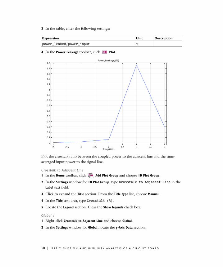
3 In the table, enter the following settings:
4 In the Power Leakage toolbar, click Plot.
Plot the crosstalk ratio between the coupled power to the adjacent line and the time-averaged input power to the signal line.
Crosstalk to Adjacent Line1 In the Home toolbar, click Add Plot Group and choose 1D Plot Group.
2 In the Settings window for 1D Plot Group, type Crosstalk to Adjacent Line in the Label text field.
3 Click to expand the Title section. From the Title type list, choose Manual.
4 In the Title text area, type Crosstalk (%).
5 Locate the Legend section. Clear the Show legends check box.
Global 11 Right-click Crosstalk to Adjacent Line and choose Global.
2 In the Settings window for Global, locate the y-Axis Data section.
Expression Unit Description
power_leaked/power_input %
50 | B A S I C E M I S S I O N A N D I M M U N I T Y A N A L Y S I S O F A C I R C U I T B O A R D

3 In the table, enter the following settings:
4 In the Crosstalk to Adjacent Line toolbar, click Plot.
The emission analysis from the circuit board inside an enclosure with a small window is finished. The next study assumes the noise source is located outside the enclosure. You will see the impact on the circuit board.
A D D S T U D Y
1 In the Home toolbar, click Add Study to open the Add Study window.
2 Go to the Add Study window.
3 Find the Studies subsection. In the Select Study tree, select General Studies>
Frequency Domain.
4 Click Add Study in the window toolbar.
5 In the Home toolbar, click Add Study to close the Add Study window.
S T U D Y 2 - I M M U N I T Y
1 In the Model Builder window, click Study 2.
Expression Unit Description
abs(emw.Pelement_2)/power_input %
51 | B A S I C E M I S S I O N A N D I M M U N I T Y A N A L Y S I S O F A C I R C U I T B O A R D

2 In the Settings window for Study, type Study 2 - Immunity in the Label text field.
3 Locate the Study Settings section. Clear the Generate default plots check box. The default plots will not be generated. Instead, some of the plots from the first study will be duplicated after computation.
Step 1: Frequency Domain1 In the Model Builder window, under Study 2 - Immunity click Step 1: Frequency Domain.
2 In the Settings window for Frequency Domain, locate the Study Settings section.
3 In the Frequencies text field, type range(2[GHz],1[GHz],6[GHz]).
4 Locate the Physics and Variables Selection section. Select the Modify model configuration for study step check box.
5 In the Physics and variables selection tree, select Component 1 (comp1)>
Electromagnetic Waves, Frequency Domain (emw)>Lumped Port 1.
6 Click Disable.
7 In the Physics and variables selection tree, select Component 1 (comp1)>
Electromagnetic Waves, Frequency Domain (emw)>Far-Field Domain 1.
8 Click Disable.
In this study, there is no excitation source in the circuit board. Though the printed dipole antenna is activated, the far-field analysis of the antenna is not of interest.
9 In the Home toolbar, click Compute.
R E S U L T S
Electric Field (emw) - Circuit Board, Immunity1 In the Model Builder window, right-click Electric Field (emw) - Circuit Board and choose
Duplicate.
2 In the Settings window for 3D Plot Group, type Electric Field (emw) - Circuit Board, Immunity in the Label text field.
3 Locate the Data section. From the Dataset list, choose Study 2 - Immunity/
Solution 2 (sol2).
4 Click the Zoom Extents button in the Graphics toolbar.
5 In the Electric Field (emw) - Circuit Board, Immunity toolbar, click Plot.
6 In the Model Builder window, expand the Electric Field (emw) - Circuit Board, Immunity node.
52 | B A S I C E M I S S I O N A N D I M M U N I T Y A N A L Y S I S O F A C I R C U I T B O A R D

Deformation 11 In the Model Builder window, expand the Results>Electric Field (emw) - Circuit Board,
Immunity>Surface 1 node, then click Deformation 1.
2 In the Settings window for Deformation, locate the Scale section.
3 In the Scale factor text field, type 4e-3.
Deformation 11 In the Model Builder window, expand the Results>Electric Field (emw) - Circuit Board,
Immunity>Surface 2 node, then click Deformation 1.
2 In the Settings window for Deformation, locate the Scale section.
3 In the Scale factor text field, type 4e-3.
4 In the Electric Field (emw) - Circuit Board, Immunity toolbar, click Plot. This plot describes the field strength coupled to the circuit board and interior walls of the enclosure from the radiation of the printed dipole antenna.
Plot the coupling ratio between the coupled power to the adjacent line and the time-averaged input power to the printed dipole antenna.
Noise Coupling to Signal Line1 In the Model Builder window, right-click Crosstalk to Adjacent Line and choose Duplicate.
53 | B A S I C E M I S S I O N A N D I M M U N I T Y A N A L Y S I S O F A C I R C U I T B O A R D

2 In the Settings window for 1D Plot Group, type Noise Coupling to Signal Line in the Label text field.
3 Locate the Data section. From the Dataset list, choose Study 2 - Immunity/
Solution 2 (sol2).
Global 11 In the Model Builder window, expand the Noise Coupling to Signal Line node, then click
Global 1.
2 In the Settings window for Global, locate the y-Axis Data section.
3 In the table, enter the following settings:
4 In the Noise Coupling to Signal Line toolbar, click Plot.
In both studies, it is observed that the strongest coupled field, crosstalk, and radiation happen around 5GHz even when the printed dipole antenna is supposed to be better for the Wi-Fi frequency.
Expression Unit Description
abs(emw.Pelement_1)/power_input %
54 | B A S I C E M I S S I O N A N D I M M U N I T Y A N A L Y S I S O F A C I R C U I T B O A R D

G L O B A L D E F I N I T I O N S
Parameters 1The parameter table can be used as a simple calculator. Calculate the dominant resonant frequency of a closed cavity based on the dimension of the interior walls.
1 In the Model Builder window, under Global Definitions click Parameters 1.
2 In the Settings window for Parameters, locate the Parameters section.
3 In the table, enter the following settings:
The computed resonant frequency is about 4.8GHz. So the given structure makes the circuit and environment vulnerable around the cavity resonance though the noise source might be stronger at a different frequency.
Name Expression Value Description
f_TE101 sqrt((pi/50[mm])^2+(pi/40[mm])^2)/(2*pi*sqrt(mu0_const*epsilon0_const))
4.799E9 1/s TE101 mode cavity resonant frequency
55 | B A S I C E M I S S I O N A N D I M M U N I T Y A N A L Y S I S O F A C I R C U I T B O A R D

56 | B A S I C E M I S S I O N A N D I M M U N I T Y A N A L Y S I S O F A C I R C U I T B O A R D